development of a high dynamic range pixel array …bigbro.biophys.cornell.edu/publications/34f...
TRANSCRIPT

DEVELOPMENT OF A HIGH DYNAMIC RANGEPIXEL ARRAY DETECTOR FOR SYNCHROTRONS
AND XFELS
A Dissertation
Presented to the Faculty of the Graduate School
of Cornell University
in Partial Fulfillment of the Requirements for the Degree of
Doctor of Philosophy
by
Joel T. Weiss
December 2017

© 2017 Joel Weiss
ALL RIGHTS RESERVED

DEVELOPMENT OF A HIGH DYNAMIC RANGE PIXEL ARRAY DETECTOR
FOR SYNCHROTRONS AND XFELS
Joel T. Weiss, Ph.D.
Cornell University 2017
Advances in synchrotron radiation light source technology have opened new
lines of inquiry in material science, biology, and everything in between. How-
ever, x-ray detector capabilities must advance in concert with light source tech-
nology to fully realize experimental possibilities. X-ray free electron lasers
(XFELs) place particularly large demands on the capabilities of detectors, and
developments towards diffraction-limited storage ring sources also necessitate
detectors capable of measuring very high flux [1–3]. The detector described
herein builds on the Mixed Mode Pixel Array Detector (MM-PAD) framework,
developed previously by our group to perform high dynamic range imaging,
and the Adaptive Gain Integrating Pixel Detector (AGIPD) developed for the
European XFEL by a collaboration between Deustsches Elektronen-Synchrotron
(DESY), the Paul-Scherrer-Institute (PSI), the University of Hamburg, and the
University of Bonn, led by Heinz Graafsma [4, 5]. The feasibility of combin-
ing adaptive gain with charge removal techniques to increase dynamic range in
XFEL experiments is assessed by simulating XFEL scatter with a pulsed infrared
laser. The strategy is incorporated into pixel prototypes which are evaluated
with direct current injection to simulate very high incident x-ray flux.
A fully functional 16x16 pixel hybrid integrating x-ray detector featuring
several different pixel architectures based on the prototypes was developed.
This dissertation describes its operation and characterization. To extend dy-

namic range, charge is removed from the integration node of the front-end am-
plifier without interrupting integration. The number of times this process oc-
curs is recorded by a digital counter in the pixel. The parameter limiting full
well is thereby shifted from the size of an integration capacitor to the depth of
a digital counter. The result is similar to that achieved by counting pixel array
detectors, but the integrators presented here are designed to tolerate a sustained
flux >1011 x-rays/pixel/second. In addition, digitization of residual analog sig-
nals allows sensitivity for single x-rays or low flux signals. Pixel high flux lin-
earity is evaluated by direct exposure to an unattenuated synchrotron source x-
ray beam and flux measurements of more than 1010 9.52 keV x-rays/pixel/s are
made. Detector sensitivity to small signals is evaluated and dominant sources
of error are identified. These new pixels boast multiple orders of magnitude
improvement in maximum sustained flux over the MM-PAD, which is capable
of measuring a sustained flux in excess of 108 x-rays/pixel/second while main-
taining sensitivity to smaller signals, down to single x-rays.

BIOGRAPHICAL SKETCH
Joel Weiss was born in Orlando Florida in 1988. He grew up there with his
parents, two brothers, and a dog named Buck. In 2007 he began college at the
University of Florida majoring in physics. He graduated with a Bachelor of Sci-
ence degree in 2011 and began graduate studies in physics at Cornell University
later that year.
iii

This document is dedicated to my family.
iv
ACKNOWLEDGEMENTS
The work described in this dissertation would not have been possible without
the help and guidance of the Gruner group’s members and many others.
Sol Gruner’s curiosity and general excitement for science and discovery is
contagious. His ability to maintain a broad view while delving into details has
been the foundation of the work described here, and his steady guidance over
the last six years has shaped me as a scientist. Mark Tate’s apparent mastery
of every project in the Gruner group still boggles my mind, and his work ethic
is unmatched. He’s been a role model for me and effectively a second adviser.
Talking through details with him is always enlightening.
Hugh Philipp has been a constant teacher to me and is a great person to
work a synchrotron night shift with (especially if there are tricycles). His ex-
pertise has been essential to this work and I’ve learned a tremendous amount
about circuit design through discussions with him. I’ve had the good fortune to
work closely with Kate Shanks on a number of projects, including the work on
uranium dioxide described in Chapter 3. She taught me all about x-ray detec-
tors when I joined the group and brings an unparallelled level of organization
to any project she touches. Her fastidiousness was essential to the completion
of the HDR-PAD. I’m lucky to call her both a colleague and a friend.
Prafull Purohit has taught me a lot about FPGAs and computer technology
while performing all of our FPGA programming. He’s also demonstrated im-
mense patience when inundated by my requests for FPGA modifications and
feature additions. Darol Chamberlain provided invaluable knowledge and ex-
perience, and I learned a lot from him as well. He always went out of his way
to help with circuit analysis or a soldering iron.
Martin Novak’s expertise has been essential to this work as he built the ma-
v

jority of mechanical components. He always knows the best way to build what-
ever it is you need, including a dog trap. I feel fortunate to have shared an office
with Jeney Wierman. She brings cheer everywhere she goes and makes positive
impacts both inside and outside of work. Veronica Pillar has also been a great
friend, and I’m glad to have learned circuits by working through Horwitz and
Hill with her.
The work described in Chapter 3 was conducted in collaboration with scien-
tists from Idaho National Lab including Krzysztof Gofryk and Daniel Antonio.
Developing the experiment on uranium dioxide with them was exciting and I
learned a great deal. Jacob Ruff was the initial driving force in this experiment,
and helped me to perform the final test of the HDR-PAD described in Chapter
7. I admire his straightforward approach to problems and depth of knowledge.
The work at the APS would not have been possible without Zahir Islam. I’ve
thoroughly enjoyed working closely with him during my trips to Illinois, and
I’ve learned a tremendous amount from him, the least of which includes the
best places to eat in Lemont. He’s been a great teacher and mentor.
The work described in Chapter 4 was performed with Julian Becker, who
helped me design the laser system before he had even arrived in our group as
a postdoctoral researcher. I’ve learned a lot from him as well. I want to thank
Professors Veit Elser and Alyssa Apsel for serving on my committee and for
their guidance throughout my work at Cornell. The foundation of my analog
integrated circuit experience comes from Professor Apsel through her course on
the topic.
My interest in physics was fostered in high school by my exceptional physics
teacher Angela Cortez who I am lucky to have learned from. Professor Stephen
Hagen introduced me to research while at the University of Florida. Though the
vi

particulars of my work have changed, he gave me the foundational skills and
understanding that I’ve used in research ever since.
My parents have always been supportive and their hard work is a constant
inspiration. The family they’ve built is a foundation on which I try to build,
and any good I can do is thanks to them. Likewise my brothers Josh and Micah
are both individuals that I look up to and admire. They set examples for me
to follow as they forge their unique paths. Micah, Josh, and Sarah are each
supportive in their own right and live with principals that I strive to emulate.
Alex’s support has been invaluable and has helped me through the toughest
stretches of graduate school.
I’ve had the pleasure to work with many other collaborators that I have
not named here, but to everyone, thank you. This research was supported
by the U.S. National Science Foundation and the U.S. National Institutes of
Health/National Institute of General Medical Sciences via NSF award DMR-
1332208, U.S. Department of Energy Award DE-FG02-10ER46693 and DE-
SC0016035, and the W. M. Keck Foundation. This work is based in part upon
research conducted at the Cornell High Energy Synchrotron Source (CHESS)
which is supported by the National Science Foundation under award DMR-
1332208. This research used resources of the Advanced Photon Source, a U.S.
Department of Energy (DOE) Office of Science User Facility operated for the
DOE Office of Science by Argonne National Laboratory under Contract No. DE-
AC02-06CH11357.
vii
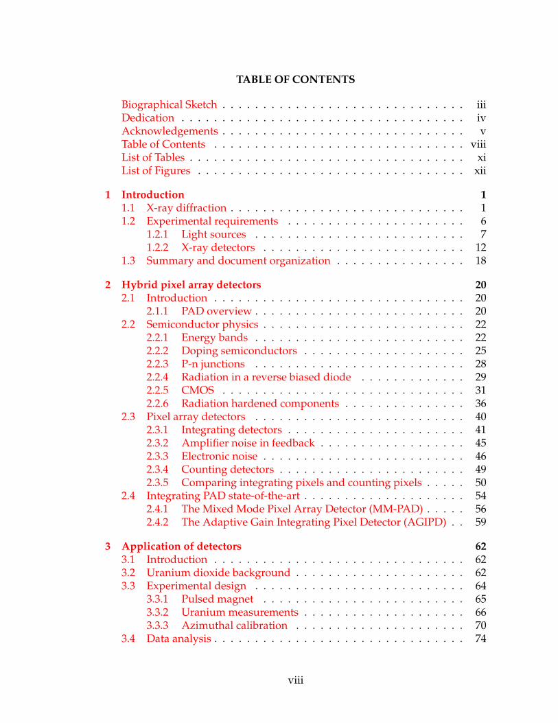
TABLE OF CONTENTS
Biographical Sketch . . . . . . . . . . . . . . . . . . . . . . . . . . . . . . iiiDedication . . . . . . . . . . . . . . . . . . . . . . . . . . . . . . . . . . . ivAcknowledgements . . . . . . . . . . . . . . . . . . . . . . . . . . . . . . vTable of Contents . . . . . . . . . . . . . . . . . . . . . . . . . . . . . . . viiiList of Tables . . . . . . . . . . . . . . . . . . . . . . . . . . . . . . . . . . xiList of Figures . . . . . . . . . . . . . . . . . . . . . . . . . . . . . . . . . xii
1 Introduction 11.1 X-ray diffraction . . . . . . . . . . . . . . . . . . . . . . . . . . . . . 11.2 Experimental requirements . . . . . . . . . . . . . . . . . . . . . . 6
1.2.1 Light sources . . . . . . . . . . . . . . . . . . . . . . . . . . 71.2.2 X-ray detectors . . . . . . . . . . . . . . . . . . . . . . . . . 12
1.3 Summary and document organization . . . . . . . . . . . . . . . . 18
2 Hybrid pixel array detectors 202.1 Introduction . . . . . . . . . . . . . . . . . . . . . . . . . . . . . . . 20
2.1.1 PAD overview . . . . . . . . . . . . . . . . . . . . . . . . . . 202.2 Semiconductor physics . . . . . . . . . . . . . . . . . . . . . . . . . 22
2.2.1 Energy bands . . . . . . . . . . . . . . . . . . . . . . . . . . 222.2.2 Doping semiconductors . . . . . . . . . . . . . . . . . . . . 252.2.3 P-n junctions . . . . . . . . . . . . . . . . . . . . . . . . . . 282.2.4 Radiation in a reverse biased diode . . . . . . . . . . . . . 292.2.5 CMOS . . . . . . . . . . . . . . . . . . . . . . . . . . . . . . 312.2.6 Radiation hardened components . . . . . . . . . . . . . . . 36
2.3 Pixel array detectors . . . . . . . . . . . . . . . . . . . . . . . . . . 402.3.1 Integrating detectors . . . . . . . . . . . . . . . . . . . . . . 412.3.2 Amplifier noise in feedback . . . . . . . . . . . . . . . . . . 452.3.3 Electronic noise . . . . . . . . . . . . . . . . . . . . . . . . . 462.3.4 Counting detectors . . . . . . . . . . . . . . . . . . . . . . . 492.3.5 Comparing integrating pixels and counting pixels . . . . . 50
2.4 Integrating PAD state-of-the-art . . . . . . . . . . . . . . . . . . . . 542.4.1 The Mixed Mode Pixel Array Detector (MM-PAD) . . . . . 562.4.2 The Adaptive Gain Integrating Pixel Detector (AGIPD) . . 59
3 Application of detectors 623.1 Introduction . . . . . . . . . . . . . . . . . . . . . . . . . . . . . . . 623.2 Uranium dioxide background . . . . . . . . . . . . . . . . . . . . . 623.3 Experimental design . . . . . . . . . . . . . . . . . . . . . . . . . . 64
3.3.1 Pulsed magnet . . . . . . . . . . . . . . . . . . . . . . . . . 653.3.2 Uranium measurements . . . . . . . . . . . . . . . . . . . . 663.3.3 Azimuthal calibration . . . . . . . . . . . . . . . . . . . . . 70
3.4 Data analysis . . . . . . . . . . . . . . . . . . . . . . . . . . . . . . . 74
viii

3.4.1 Future work . . . . . . . . . . . . . . . . . . . . . . . . . . . 773.5 Necessity of high dynamic range . . . . . . . . . . . . . . . . . . . 77
4 The high dynamic range detector concept 804.1 Measuring the plasma effect . . . . . . . . . . . . . . . . . . . . . . 81
4.1.1 Experimental apparatus . . . . . . . . . . . . . . . . . . . . 834.1.2 Transient current analysis . . . . . . . . . . . . . . . . . . . 884.1.3 Conclusions . . . . . . . . . . . . . . . . . . . . . . . . . . . 94
4.2 Adaptive gain and charge removal combined . . . . . . . . . . . . 95
5 Pixel substructure testing 975.1 Pixel architectures . . . . . . . . . . . . . . . . . . . . . . . . . . . . 98
5.1.1 MM-PAD 2.0 . . . . . . . . . . . . . . . . . . . . . . . . . . 995.1.2 Charge dump oscillator . . . . . . . . . . . . . . . . . . . . 1025.1.3 Capacitor flipping pixel . . . . . . . . . . . . . . . . . . . . 105
5.2 Integrating amplifier . . . . . . . . . . . . . . . . . . . . . . . . . . 1085.2.1 Flipped voltage follower . . . . . . . . . . . . . . . . . . . . 1105.2.2 Local common mode feedback . . . . . . . . . . . . . . . . 1125.2.3 Amplifier output . . . . . . . . . . . . . . . . . . . . . . . . 1145.2.4 Noise properties . . . . . . . . . . . . . . . . . . . . . . . . 1165.2.5 Pole splitting . . . . . . . . . . . . . . . . . . . . . . . . . . 116
5.3 Current injection tests . . . . . . . . . . . . . . . . . . . . . . . . . 1195.3.1 Probe pad current injection . . . . . . . . . . . . . . . . . . 1205.3.2 Performance and analysis . . . . . . . . . . . . . . . . . . . 122
5.4 Summary . . . . . . . . . . . . . . . . . . . . . . . . . . . . . . . . . 126
6 The high dynamic range pixel array detector 1276.1 Introduction . . . . . . . . . . . . . . . . . . . . . . . . . . . . . . . 1276.2 System overview . . . . . . . . . . . . . . . . . . . . . . . . . . . . 1276.3 HDR-PAD ASIC . . . . . . . . . . . . . . . . . . . . . . . . . . . . . 131
6.3.1 Pixel overview . . . . . . . . . . . . . . . . . . . . . . . . . 1326.3.2 Data readout . . . . . . . . . . . . . . . . . . . . . . . . . . 1346.3.3 Adaptive gain implementation . . . . . . . . . . . . . . . . 1406.3.4 Programmable test sources . . . . . . . . . . . . . . . . . . 1416.3.5 Radiation hardening . . . . . . . . . . . . . . . . . . . . . . 142
7 HDR-PAD Characterization 1477.1 Introduction . . . . . . . . . . . . . . . . . . . . . . . . . . . . . . . 147
7.1.1 Dark current integration . . . . . . . . . . . . . . . . . . . . 1487.1.2 Photon histograms . . . . . . . . . . . . . . . . . . . . . . . 1517.1.3 High flux measurements . . . . . . . . . . . . . . . . . . . . 155
7.2 Small signal resolution . . . . . . . . . . . . . . . . . . . . . . . . . 1637.2.1 Global noise sources . . . . . . . . . . . . . . . . . . . . . . 1647.2.2 Local noise . . . . . . . . . . . . . . . . . . . . . . . . . . . . 169
ix

8 Conclusions 173
A Laser pulse measurement schematics 177
x

LIST OF TABLES
4.1 Table listing some x-ray energies, their attenuation length in sil-icon, and the IR wavelength with a matching attenuation lengthin room temperature silicon. X-ray attenuation lengths weredrawn from the NIST database [64], and IR photon attenuationlengths were drawn from [65]. . . . . . . . . . . . . . . . . . . . . 82
5.1 Pixel Average Power Consumption From Simulation . . . . . . . 125
6.1 Pixel front-end specifications . . . . . . . . . . . . . . . . . . . . . 134
7.1 Parameters extracted from photon histograms . . . . . . . . . . . 1557.2 Power supply variability . . . . . . . . . . . . . . . . . . . . . . . 1687.3 Pixel noise in reset . . . . . . . . . . . . . . . . . . . . . . . . . . . 1697.4 Pixel noise in low gain . . . . . . . . . . . . . . . . . . . . . . . . . 170
xi

LIST OF FIGURES
1.1 Two scattering bodies separated by ~d. Radiation is incident withwave vector ~k and radiation is scattered with wave vector ~k′ Thepath length difference between light scattering from one pointversus the other is ~d · (n − n′). . . . . . . . . . . . . . . . . . . . . . 2
1.2 LEFT: a bending magnet steers an electron beam and producesradiation throughout the curved motion. MIDDLE: A wigglerinduces sinusoidal motion in an electron beam and produces acone of radiation which sweeps from side to side. RIGHT: Anundulator induces sinusoidal motion in an electron beam andproduces a cone of radiation which maintains an overlappingportion while sweeping from side to side. Figure adapted from[15]. . . . . . . . . . . . . . . . . . . . . . . . . . . . . . . . . . . . 8
1.3 Schematic of SASE FEL insertion device. Long undulators areused such that light produced by the mild sinusoidal motion ofelectrons at the start of the beam segment modulate the spa-tial density of electrons further along. The resultant electronbunching causes electrons to amplify the radiation coherently.Adapted from [13]. . . . . . . . . . . . . . . . . . . . . . . . . . . . 11
1.4 Percent of x-rays absorbed in 500µm silicon at normal incidence.Attenuation length data from [23]. . . . . . . . . . . . . . . . . . . 16
2.1 A cartoon schematic of a hybrid pixel array detector. The CMOSelectronics layer is a lattice of pixel-circuits which measure sig-nals coming from the diode detection layer. The diode detectionlayer converts incident radiation into an electronic signal. Thebump bonds connect the diode detection layer and CMOS elec-tronics layer on a per-pixel basis, transferring electronic signalsfrom the region of the detection layer in which radiation was ab-sorbed to the nearest pixels. The image is adapted from [28] andis not to scale. . . . . . . . . . . . . . . . . . . . . . . . . . . . . . . 21
2.2 (a) Allowed energies of an electron in a one dimensional sinu-soidal potential with periodicity a. When the wave vector isequal to an integer multiple of reciprocal lattice vectors, two so-lutions to the Schrodinger equation exist corresponding to stand-ing waves with peaks on or between the potential peaks. (b) Theallowed energies wrapped back and depicted as bands in the”reduced zone scheme.“ Image adapted from [33]. . . . . . . . . 24
xii

2.3 Cartoon depiction of electron pairing in a silicon crystal. Notethat the diamond structure of the lattice is not represented here.Only valence electrons are drawn. (a) Silicon atom in perfect lat-tice. Four valence electrons make covalent bonds with all nearestneighboring atoms. (b) One boron atom replaces a silicon atom.A hole is present because the boron has only three valence elec-trons and cannot bond with all four nearest neighbors. (c) Onephosphorus atom replaces a silicon atom. Four of the five phos-phorus valence electrons engage in covalent bonding. The fifthvalence electron occupies a state in the conduction band. . . . . . 27
2.4 Cartoon depiction of radiation being absorbed in a reverse bi-ased diode. The image is not to scale. The clouds of charge car-riers formed are offset in this image for clarity. The aluminumcontact on the sensor is labeled. Image adapted form [36]. . . . . 31
2.5 N-type MOSFET transistor cross-section. The four transistor ter-minals are the source, drain, gate, and substrate. Width andlength (W and L respectively) describe the dimensions of theconductive channel formed beneath the gate when inverted. Im-age adapted from [37] with alterations. . . . . . . . . . . . . . . . 32
2.6 Photo of the CS-PAD hybridized ASIC wirebonded to supportelectronics. The wirebonds send biases and control signals to theASIC, and also transmit readout signals from pixels to supportelectronics for processing and recording. The silicon sensor layeris about 20mm wide. (photograph by Mark W. Tate) . . . . . . . 41
2.7 MM-PAD ASIC bump bonds. The ASIC contains a 128x128 ar-ray of solder bumps, one connected to each pixel, which can bebonded to a sensor with suitable backside metalization. Pixelpitch is 150µm. . . . . . . . . . . . . . . . . . . . . . . . . . . . . . 42
2.8 Basic integrating pixel schematic. The diode represents a con-nection to the photodiode sensor. The amplifier collects chargeincident from the photodiode onto C f . Cd is not a real capacitor,but represents the parasitic capacitance on the front end of thepixel. Vout is the pixel output, typically digitized outside of thepixel through an analog transmission chain (not shown). . . . . . 43
2.9 Basic counting pixel schematic. The diode represents a connec-tion to the photodiode sensor. Cd is not a real capacitor, but rep-resents the parasitic capacitance on the front end of the pixel. Thepulse shaper outputs a pulse for incident photocurrent spikes.The comparator determines whether the pulse height indicatesthat an x-ray was absorbed in the sensor. When the comparatorfires, the counter in incremented. The total digital counts in agiven period are readout off chip (read out chain not shown). . . 49
xiii
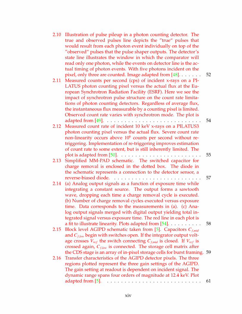
2.10 Illustration of pulse pileup in a photon counting detector. Thetrue and observed pulses line depicts the ”true“ pulses thatwould result from each photon event individually on top of the”observed“ pulses that the pulse shaper outputs. The detector’sstate line illustrates the window in which the comparator willread only one photon, while the events on detector line is the ac-tual timing of photon events. With five photons incident on thepixel, only three are counted. Image adapted from [48]. . . . . . . 52
2.11 Measured counts per second (cps) of incident x-rays on a PI-LATUS photon counting pixel versus the actual flux at the Eu-ropean Synchrotron Radiation Facility (ESRF). Here we see theimpact of synchrotron pulse structure on the count rate limita-tions of photon counting detectors. Regardless of average flux,the instantaneous flux measurable by a counting pixel is limited.Observed count rate varies with synchrotron mode. The plot isadapted from [49]. . . . . . . . . . . . . . . . . . . . . . . . . . . . 54
2.12 Measured count rate of incident 10 keV x-rays on a PILATUS3photon counting pixel versus the actual flux. Severe count ratenon-linearity occurs above 106 counts per second without re-triggering. Implementation of re-triggering improves estimationof count rate to some extent, but is still inherently limited. Theplot is adapted from [50]. . . . . . . . . . . . . . . . . . . . . . . . 55
2.13 Simplified MM-PAD schematic. The switched capacitor forcharge removal is enclosed in the dotted box. The diode inthe schematic represents a connection to the detector sensor, areverse-biased diode. . . . . . . . . . . . . . . . . . . . . . . . . . 57
2.14 (a) Analog output signals as a function of exposure time whileintegrating a constant source. The output forms a sawtoothwave, dropping each time a charge removal cycle is executed.(b) Number of charge removal cycles executed versus exposuretime. Data corresponds to the measurements in (a). (c) Ana-log output signals merged with digital output yielding total in-tegrated signal versus exposure time. The red line in each plot isa fit to illustrate linearity. Plots adapted from [54]. . . . . . . . . . 58
2.15 Block level AGIPD schematic taken from [5]. Capacitors C f ,mid
and C f ,low begin with switches open. If the integrator output volt-age crosses Vre f the switch connecting C f ,mid is closed. If Vre f iscrossed again, C f ,low is connected. The storage cell matrix afterthe CDS stage is an array of in-pixel storage cells for burst framing. 59
2.16 Transfer characteristics of the AGIPD detector pixels. The threeregions plotted represent the three gain settings of the AGIPD.The gain setting at readout is dependent on incident signal. Thedynamic range spans four orders of magnitude at 12.4 keV. Plotadapted from [5]. . . . . . . . . . . . . . . . . . . . . . . . . . . . 61
xiv

3.1 The sample is mounted in the magnet and diffraction is collectedby the detector in back-scatter geometry. Note that the sampledoes not rotate independently from the magnet. . . . . . . . . . . 67
3.2 Sample θ measures the rotation of the sample relative to the in-cident beam. 2θ measures the angle of diffraction relative to thetransmitted beam. . . . . . . . . . . . . . . . . . . . . . . . . . . . 68
3.3 Detector pixels are mapped horizontally to diffraction angles(2θ). Detector pixels are summed in the vertical direction (χ) tocreate the θ − 2θ plots referred to throughout this chapter. Dueto sample orientation, diffraction primarily occurs in the y-x plane. 68
3.4 Uranium dioxide θ−2θ plot measured at zero field and 14 K. Thevertical lines in the intensity are artifacts resulting from gaps be-tween the MM-PAD detector modules. This plot serves as a base-line for comparison of diffraction from the sample with magneticfields applied. . . . . . . . . . . . . . . . . . . . . . . . . . . . . . . 69
3.5 Sample frame of uranium dioxide diffraction peak 〈888〉 at roomtemperature. The color scale is logrithmic and the exposure timewas 10 ms. The peak flux is close to the maximum measurableby the MM-PAD. Gaps between the modules of the MM-PAD arealso visible. . . . . . . . . . . . . . . . . . . . . . . . . . . . . . . . 70
3.6 Pulsed magnetic field as measured by the Hall current monitor,based on the known inductance of the solenoid. To illustratemagnetic field sampling, MM-PAD exposures are highlighted.Each exposure time was 140µs. . . . . . . . . . . . . . . . . . . . . 71
3.7 Pixel to 2θ calibration geometry. Diffraction from a siliconmonochromator is measured with two different x-ray energiesand fixed detector position. This allows calculation of the az-imuthal angular position of each pixel on the detector surface. . . 73
3.8 A selection of θ − 2θ plots of uranium dioxide as a function ofmagnetic field. Each plot is composed of a separate frame foreach sample θ value. Values of 2θ correspond to pixels on theMM-PAD. This depiction illustrates the behavior of electron den-sity in reciprocal space as a function of magnetic field. . . . . . . 75
3.9 Integrated intensity along reciprocal lattice vector 〈hhh〉 as afunction of magnetic field. At zero field a single diffraction peakis seen. The peak shifts as field increases, and a weaker peak di-verges from the primary diffraction above 5 T. The plot is formedby dividing θ− 2θ plots along the line θ = θ into bins perpendic-ular to this line, spanning the entire dataset. The top and bottomimages are the same data. The top plot has a linear scale and thebottom plot has a log scale. . . . . . . . . . . . . . . . . . . . . . . 76
xv

4.1 Attenuation length in silicon of x-rays (left) matches attenuationlength in silicon of IR photons (right). The green line highlightsthe correspondence of 12 keV photons to 1016 nm photons. Inthis way, IR laser pulses can simulate XFEL pulses. . . . . . . . . 82
4.2 Simulated hole density created in one micron slices of a siliconsensor as a function of depth into the sensor for a laser pulse of1016 nm wavelength photons with various spectral distributionsat normal incidence. The laser pulse was simulated with 6 µmpulse radius and 1011 eV pulse energy at room temperature. . . . 84
4.3 Laser beam path for transient current technique studies. Thepulsed infrared laser is controlled by a computer (not shown)which coordinates the oscilloscope readings. Laser pulses passthrough a beam sampler which consists of an 1% silvered mir-ror at 45 degrees to the beam path. A dedicated diode readsthe fractional pulse to record pulse-to-pulse energy variations.The main pulse then passes through a filter wheel which enableslarge scale pulse intensity variation. The pulse is subsequentlyexpanded through a Galilean telescope to permit tighter focusby the achromatic doublet lens. The focused pulse is absorbedby a custom silicon photo diode and the photocurrent transientis routed to the oscilloscope through a custom PCB. The mainpulse transient and split pulse transient are read by the oscillo-scope to the data acquisition computer. . . . . . . . . . . . . . . . 86
4.4 Gaussian fit to derivative of lateral translation scan of targetdiode with 950nm laser incident. The fitted line describes thelaser pulse profile in one dimension perpendicular to the beampath. . . . . . . . . . . . . . . . . . . . . . . . . . . . . . . . . . . . 90
4.5 Characteristic shape of photocurrent transients produced byhigh intensity pulses (> 104 x-rays). The transient above is anaverage of one hundred 950 nm pulses (equivalent to 8 keV at-tenuation length) with a mean single pulse energy equivalent to106 8 keV x-rays. The sensor was bias was 200 V. . . . . . . . . . . 90
4.6 Normalized integrated charge versus integration time of 1016nm (12 keV equivalent attenuation length) pulses at three pulseenergies. The red dotted line is a low energy pulse (< 103 x-rays,simulated from previous work [66]) for reference. Sensor biaswas 200 V. . . . . . . . . . . . . . . . . . . . . . . . . . . . . . . . . 92
4.7 Average pulse duration as a function of total pulse energy atthree wavelengths. Pulse durations were measured as timeabove two times the standard deviation of background noise.Sensor bias was 200 V. . . . . . . . . . . . . . . . . . . . . . . . . . 92
4.8 Averaged photocurrent traces from 950nm laser pulses focusedto 6 µm incident on a 500 µm thick silicon diode. The diode biaswas 200 V. . . . . . . . . . . . . . . . . . . . . . . . . . . . . . . . . 93
xvi

5.1 Simplified MM-PAD 2.0 schematic. Control logic box engagesadaptive gain prior to enabling switched capacitor charge removal.100
5.2 MM-PAD 2.0 gated oscillator and charge removal switched ca-pacitor block level schematics. . . . . . . . . . . . . . . . . . . . . 101
5.3 Simplified CDO schematic. The ring oscillator charge removalcircuitry is enclosed in the dashed box. Selectable gain was re-placed with an adaptive gain scheme in a subsequent fabrication. 103
5.4 Simplified capacitor flipping pixel schematic. Dynamic thresh-olding circuitry is enclosed in the dotted box. An adaptive gainscheme was implemented in the most recent fabrication. . . . . . 106
5.5 Class AB amplifier topology utilized in pixel prototypes. Archi-tecture adapted from [70]. . . . . . . . . . . . . . . . . . . . . . . . 110
5.6 Example of negative feedback. . . . . . . . . . . . . . . . . . . . . 1165.7 Inferred input currents based on pixel outputs versus actual in-
put current. The dotted line represents an ideal response (in-ferred input equals actual input). The charge dump oscillatoris plotted with circles, the MM-PAD 2.0 with triangles, the exter-nally thesholded capacitor flipping pixel with diamonds, and thedynamically thesholded capacitor flipping pixel with squares.Input and inferred current values are converted to the numberof 8 keV x-rays absorbed in silicon per second which would pro-duce an equivalent photocurrent. Inset: Magnification of thesame data. . . . . . . . . . . . . . . . . . . . . . . . . . . . . . . . . 121
5.8 Measured comparator delays from the capacitor flipping pixelwith dynamic thresholding are plotted. Measured values as-sume that all deviations from linearity in the capacitor flippingpixel’s output are a result of charge integrated during switchingdelays. Values from simulation are plotted as a dotted line. . . . 123
6.1 Photograph of the high dynamic range pixel array detector(HDR-PAD) unit with FPGA, vacuum enclosure, and PCB sup-port electronics shown. Not shown are power supply units,controlling computer, vacuum, water chiller, and thermoelectriccontroller. The vacuum housing is roughly four inches alongeach edge. . . . . . . . . . . . . . . . . . . . . . . . . . . . . . . . . 128
6.2 LEFT: ZIF socket on the support electronics PCB with thermallyregulated cold finger protruding. The PCB metalization which issandwiched by the clam shell assembly is visible. RIGHT: Hy-bridized module wire bonded to a ceramic pin grid array (PGA)package, seated in the ZIF socket. The cold finger makes contactwith the backside of the packaging. . . . . . . . . . . . . . . . . . 129
xvii
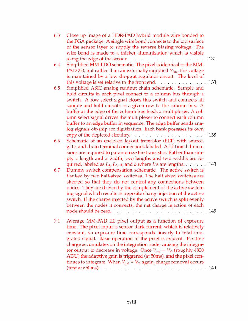
6.3 Close up image of a HDR-PAD hybrid module wire bonded tothe PGA package. A single wire bond connects to the top surfaceof the sensor layer to supply the reverse biasing voltage. Thewire bond is made to a thicker aluminization which is visiblealong the edge of the sensor. . . . . . . . . . . . . . . . . . . . . . 131
6.4 Simplified MM-LDO schematic. The pixel is identical to the MM-PAD 2.0, but rather than an externally supplied Vlow, the voltageis maintained by a low dropout regulator circuit. The level ofthis voltage is set relative to the front end. . . . . . . . . . . . . . 133
6.5 Simplified ASIC analog readout chain schematic. Sample andhold circuits in each pixel connect to a column bus through aswitch. A row select signal closes this switch and connects allsample and hold circuits in a given row to the column bus. Abuffer at the edge of the column bus feeds a multiplexer. A col-umn select signal drives the multiplexer to connect each columnbuffer to an edge buffer in sequence. The edge buffer sends ana-log signals off-ship for digitization. Each bank posesses its owncopy of the depicted circuitry. . . . . . . . . . . . . . . . . . . . . . 138
6.6 Schematic of an enclosed layout transistor (ELT) with source,gate, and drain terminal connections labeled. Additional dimen-sions are required to parametrize the transistor. Rather than sim-ply a length and a width, two lengths and two widths are re-quired, labeled as L1, L2, a, and b where L’s are lengths. . . . . . . 143
6.7 Dummy switch compensation schematic. The active switch isflanked by two half-sized switches. The half sized switches areshorted so that they do not control any connections betweennodes. They are driven by the complement of the active switch-ing signal which results in opposite charge injection of the activeswitch. If the charge injected by the active switch is split evenlybetween the nodes it connects, the net charge injection of eachnode should be zero. . . . . . . . . . . . . . . . . . . . . . . . . . . 145
7.1 Average MM-PAD 2.0 pixel output as a function of exposuretime. The pixel input is sensor dark current, which is relativelyconstant, so exposure time corresponds linearly to total inte-grated signal. Basic operation of the pixel is evident. Positivecharge accumulates on the integration node, causing the integra-tor output to decrease in voltage. Once Vout = Vth (roughly 4800ADU) the adaptive gain is triggered (at 50ms), and the pixel con-tinues to integrate. When Vout = Vth again, charge removal occurs(first at 650ms). . . . . . . . . . . . . . . . . . . . . . . . . . . . . . 149
xviii
7.2 Cartoon depiction of pinhole mask alignment. Pin holes aresmaller than pixels and spaced more than one pixel width apart.Aligning the pinholes over the center of pixels ensures that thesignal from each photon absorbed by a pixel is not shared withneighboring pixels. . . . . . . . . . . . . . . . . . . . . . . . . . . . 152
7.3 Histogram of 25,000 analog outputs from an MM-LDO pixelwith low flux silver kα radiation. Exposure time was 1 ms. Thehistogram is fit by a sum of five Gaussian functions. Parametersfrom the fit describe the pixel’s gain and noise characteristics.Peaks corresponding to integer numbers of photons absorbed bythe pixel in the integration window are labeled. . . . . . . . . . . 153
7.4 Photon histograms of MM-LDO pixels with progressively higherflux. Photon peaks are fit from zero photons up to twenty-onephotons. A final peak was added where a twenty-second peakwould sit. This signal level triggers the adaptive gain circuitryand brings the pixel integrator output away from the thresholdvoltage. . . . . . . . . . . . . . . . . . . . . . . . . . . . . . . . . . 156
7.5 CHESS A2 beamline schematic. Beam enters the hutch throughbeam defining slits and enters the first ion chamber (IC1) whichmeasures the full beam flux. A variable attenuator rotates toplace aluminum of various thicknesses in the path of the beam.A second ion chamber (IC2) measures the attenuated flux. Theattenuated beam strikes the HDR-PAD directly. . . . . . . . . . . 158
7.6 Sample image with 1 ms exposure to the full A2 beam. The scaleis logarithmic. . . . . . . . . . . . . . . . . . . . . . . . . . . . . . . 158
7.7 Signal measured by the MM-PAD 2.0 pixel with a total integra-tion capacitance of 880 fF versus the signal measured by ionchambers. The dashed line represents perfect performance forcomparison. . . . . . . . . . . . . . . . . . . . . . . . . . . . . . . . 159
7.8 Signal measured by the MM-PAD 2.0 pixel with a total integra-tion capacitance of 2630 fF versus the signal measured by ionchambers. The dashed line represents perfect performance forcomparison. . . . . . . . . . . . . . . . . . . . . . . . . . . . . . . . 160
7.9 Signal measured by the capacitor flipping pixel with an exter-nally supplied threshold voltage versus the signal measured byion chambers. The dashed line represents perfect performancefor comparison. . . . . . . . . . . . . . . . . . . . . . . . . . . . . . 161
7.10 Signal measured by the capacitor flipping pixel with dynamicthresholding enabled versus the signal measured by ion cham-bers. The dashed line represents perfect performance for com-parison. . . . . . . . . . . . . . . . . . . . . . . . . . . . . . . . . . 162
7.11 Signal measured by the MM-LDO pixel versus the signal mea-sured by ion chambers. The dashed line represents perfect per-formance for comparison. . . . . . . . . . . . . . . . . . . . . . . . 162
xix

7.12 Pixel bank average versus pixel bank average. Each point repre-sents one frame. Bank averages from within the same frame arecompared. Correlation coefficient is computed. . . . . . . . . . . 164
7.13 The standard deviation of N pixels averaged together is plottedas a blue dotted line. The average standard deviation of N pixelsdivided by N is plotted as an orange dashed line. If there wereno global noise, the standard deviation of the average value ofmany pixels would approach zero as N increases. . . . . . . . . . 166
A.1 Layout of sample PCB used in pulsed infrared laser studies dis-cussed in Chapter 4. The circle labeled HV on the right side ofthe board is punched through to permit laser pulses to strike thediode, which is connected to the ring which supplies the biasvoltage. Immediately to the left of this ring are wire bondingpads which are connected directly to pixels on the diode. Sig-nals are routed through a connector to the circuitry for whichschematics are provided on subsequent pages. . . . . . . . . . . . 177
xx

CHAPTER 1
INTRODUCTION
X-rays are used to obtain structural information about samples on the atomic
scale. This experimental probe finds applications in fields from material science
to biology and everything in-between. Each experiment requires an x-ray light
source and a sample, but they also require a suitable x-ray detector or means of
measuring the experimental output. New x-ray light sources require new x-ray
detectors with commensurate capabilities. This thesis outlines the development
of such a detector suitable for use at new, high brightness x-ray sources. By
extending the measurable dynamic range, light sources can be utilized to their
full potential.
1.1 X-ray diffraction
To probe matter on the atomic scale, we need photons with wavelengths of the
appropriate size. Visible photons have wavelengths that are several hundreds
of nanometers. These photons interact with a large number of atoms simul-
taneously when they strike an object because atomic spacing in matter is on
the order of angstroms, 10−10m. This corresponds to a photon energy of cλ
=
12.4keV, which is the realm of x-rays. To understand how x-rays interact with
matter, we will base our discussion on the derivation of the Von Laue formu-
lation of x-ray diffraction in Solid State Physics by Ashcroft and Mermin [6].
To simplify the discussion, we will assume that the scattering of photons from
matter is elastic, meaning that no energy is lost in the scattering process, and
thus the wavelength of scattered light is the same as the wavelength of incident
1

light.
−ො𝑛′ ∙ Ԧ𝑑ො𝑛 ∙ Ԧ𝑑
𝑘′Ԧ𝑑
𝑘
𝑘 =2𝜋ො𝑛
𝜆
𝑘′ =2𝜋 ො𝑛′
𝜆
𝑘
𝑘′
Figure 1.1: Two scattering bodies separated by ~d. Radiation is incident withwave vector ~k and radiation is scattered with wave vector ~k′ The path lengthdifference between light scattering from one point versus the other is ~d · (n − n′).
Consider two small scattering bodies separated by a vector ~d as depicted in
Figure 1.1. Assume that light arrives at the bodies from very far away so that
the incident wave vector of each photon is parallel. The wave vector is defined
as ~k ≡ 2πnλ
where n is the unit vector parallel to ~k. Consider scattered photons
with wave vector ~k′ ≡ 2πn′λ
. To interfere constructively, the difference in length
between the two paths must be an integer multiple of the light’s wavelength:
~d · n − ~d · n′ = ~d · (n − n′) = mλ (1.1)
where m is an integer. Multiplying both sides of the equation above by 2πλ
yields
~d · (~k − ~k′) = 2πm. (1.2)
2

Now applying Euler’s formula,
eix = cos(x) + i sin(x), (1.3)
we find that ∣∣∣∣ei(~k−~k′)·~d∣∣∣∣ =
∣∣∣ei2πm∣∣∣ = |cos(2πm) + i sin(2πm)| = 1. (1.4)
Finally, we can define ~K to be the change in wave vector of the scattered light:
∣∣∣∣e−i~K·~d∣∣∣∣ = 1. (1.5)
To reiterate, the equations above specify, in general terms, the spatial rela-
tion required for two bodies to scatter light that will interfere purely construc-
tively. From this calculation we can in theory perform a simple experiment to
measure the distance between two atoms, given that we scatter monochromatic
light from them and measure the angle at which the scattered light interferes
constructively. Of course we would often like to image matter that is composed
of more than two atoms.
Interestingly, Equation 1.5 is precisely the definition of the reciprocal lattice
for a Bravais lattice with points at ~d. Many sources exist for a rigorous discus-
sion of Bravais lattices and crystals in general (for example see [6, 7]). Here we
will outline the concept briefly.
A given Bravais lattice is defined by its basis vectors. In three dimensions
a set of Bravais basis vectors may be any three vectors which do not lie in the
same plane, and the corresponding Bravais lattice is the collection of all points
of the form ~d = m1 ~a1 + m2 ~a2 + m3 ~a3 where m1, m2, and m3 are integers and ~a1,
~a2, and ~a3 are the basis vectors [6]. Bravais lattices are used to describe crys-
talline materials, materials in which all of the constituent atoms are arranged
3

periodically. The magnitudes of a Bravais lattice’s reciprocal lattice vectors are
inversely proportional to atomic spacing and their direction is perpendicular to
atomic planes. Specifically, for lattice vectors ~a1, ~a2, and ~a3, the reciprocal lattice
vectors are
~b1 = 2π~a2 × ~a3
~a1 · (~a2 × ~a3), (1.6)
~b2 = 2π~a3 × ~a1
~a1 · (~a2 × ~a3), (1.7)
and
~b3 = 2π~a1 × ~a2
~a1 · (~a2 × ~a3). (1.8)
In the case of crystalline materials, equation 1.5 leads to the conclusion that
for constructive interference, the change in the incident wave vector must be a
linear combination of reciprocal lattice vectors. In this context, Equation 1.5 is
equivalent to the familiar Bragg condition,
2d sin θ = mλ, (1.9)
where d is the spacing between atomic planes, m is a positive integer, θ is the
angle of incidence relative to the atomic planes, and λ is the wavelength. The
derivation above does not assume specular reflection or a particular arrange-
ment of atoms. The mathematical formalism gives us a rigorous framework to
understand diffraction due to elastic scattering. In a more intuitive sense how-
ever, we find that atomic spacing can be measured by the angle at which x-rays
scatter constructively from a sample.
The work above can be used to understand scattering from non-periodic
arrangements of atoms as well. Note that Equation 1.2 specifies the condition
4

for purely constructive interference. More generally, e−i~K·~d is the difference in
phase factors between photons scattered at the origin and photons scattered at
~d [7]. Suppose we define some function ρ(~d) to be the electron density of an
object at all points in space. Assume that the amplitude of a wave scattered
from a volume element dV is proportional to the electron density of the volume
element. The amplitude of electric and magnetic fields for radiation scattered in
the direction ~k′ will be proportional to the integral over all space of the electron
density function multiplied by the term describing the phase relationship [7].
Specifically, the scattering amplitude, F, is
F =
∫~R
e−i~K·~dρ(~d)dV. (1.10)
Note that equation 1.10 is the Fourier transform of the spatial distribution of
the electron density. In this light, scatter from a periodic arrangement of atoms
is a special case in which the spatial frequency of electron density is dominated
by a discreet set of frequencies, thus sharp peaks are observed in x-ray diffrac-
tion from crystals. However, diffraction is measurable from any scattering body.
Note that the situation is more complicated when the energy of incident radia-
tion is close to the energy of an electron transition in the diffracting atoms. This
leads to so called resonant scattering which involves results of the incident x-
rays altering the distribution of electrons in the sample. For more information
on this phenomena see sources such as [8, 9].
Of course, diffraction is not the only useful measurement that can be per-
formed with x-rays. Radiography relies on the transmission of x-rays to gain
information about density variations in the material being imaged. More dense
materials absorb or scatter more x-rays, and so regions of a sample which trans-
mit a larger fraction of incident x-rays are less dense. This is the general tech-
5

nique employed in most medical x-ray imaging. Fluorescence can be utilized
to map the elemental constituents of a sample. X-rays of the correct energy
excite inner-shell electrons in atoms to outer shells or ionize the atoms com-
pletely. When an electron subsequently drops in energy to fill the now under-
filled orbital, light is emitted with energy equal to the change. This results in
characteristic energies for each element, and by exciting the atoms of a sample
and measuring the resultant fluorescence, the atomic constituents of the sam-
ple can be uncovered. Many more techniques utilizing x-rays to make useful
measurements exist, but this dissertation work focuses primarily on diffraction
experiments.
1.2 Experimental requirements
With an experimental probe for atomic scale information of a sample established
in theory, we arrive at the question: what is required to perform these measure-
ments in practice? The intricacies of experimental design and execution could
fill volumes and vary drastically between each particular implementation. We’ll
settle here for a more basic treatment. To study a sample with x-ray diffraction
requires a suitable x-ray source, a sample from which the x-rays will scatter, and
a device with which to detect the scattered x-rays.
6

1.2.1 Light sources
X-ray tube sources
The most common x-ray source in a laboratory is an x-ray tube source. An
overview of a tube source’s operation is outlined below.
Electrons are emitted from a filament. The electrons are accelerated through
a very high electric field created by a voltage difference between an anode and
a cathode. Electrons then strike the anode. X-rays are generated primarily
through two processes [10]. Bremsstrahlung radiation, or braking radiation, is
the result of electrons decelerating in the anode material. The product is a broad
spectrum of photons whose energies are limited by the voltage across which the
electrons were accelerated. The second process involves the excitation of inner
shell electrons in the anode material. Electrons are ejected from atoms in the
anode, and when an electron drops in energy to take this now vacant set of
quantum numbers, the change in energy is released as a photon. This results in
distinct photon energy emissions that vary based on the anode material.
With an x-ray tube source, the primary limitation on maximum x-ray flux
obtainable is the rate at which energy deposited in the anode as heat can be
drawn away. Only about ∼ 0.2% of the power, electron current multiplied by
acceleration voltage, is actually converted to x-ray radiation [10]. To increase
the maximum flux of tube sources, some sources employ a large, constantly
moving anode that allows deposited heat to be distributed over a larger area.
More recently, sources with a liquid metal anode have been implemented [11].
However, synchrotron radiation facilities dwarf tabletop x-ray production and
will be discussed in the next section.
7

Synchrotron radiation facilities
Synchrotron radiation facilities have evolved significantly since their inception
over 50 years ago [12]. A synchrotron is a particle accelerator in which charged
particles are set to run in a closed path at relativistic speeds. Further accelera-
tion of these charged particles produces radiation with specific characteristics.
Precise control of this acceleration allows production of light with a variety of
useful properties.
At present, over 50 synchrotron facilities are in operation worldwide, with
12 of these being so-called third generation sources [13]. Still more synchrotrons
are under construction as the demand for beam time among scientists is far
greater than its supply. Synchrotrons utilize bending magnets, wigglers, and
undulators to produce intense, collimated x-ray beams [14]. Figure 1.2 is a car-
toon depiction of radiation from these devices.
Figure 1.2: LEFT: a bending magnet steers an electron beam and produces ra-diation throughout the curved motion. MIDDLE: A wiggler induces sinusoidalmotion in an electron beam and produces a cone of radiation which sweepsfrom side to side. RIGHT: An undulator induces sinusoidal motion in an elec-tron beam and produces a cone of radiation which maintains an overlappingportion while sweeping from side to side. Figure adapted from [15].
8

Bending magnets are used to steer electron beams via the Lorentz force, but
the acceleration that they cause also produces radiation. At synchrotrons, rela-
tivistic effects compress the emitted radiation into a cone with an opening angle
in radians proportional to 1γ
where γ is the Lorentz factor [14]. Wigglers and
undulators are used at sychrotrons, in addition to bending magnets, to generat-
ing radiation with useful properties. Wigglers are a series of bending magnets
with alternating polarity which produce no net deflection of the electron beam.
Undulators have the same magnetic structure as wigglers, but the deflection
caused by their magnetic fields is small enough that the cone of radiation gen-
erated at each bend maintains an overlap in space. This causes interference of
the radiation emitted at each turn which permits generation of highly coherent
beams with sharp energy spectra [14].
In third generation light sources, light is typically emitted in pulses with
tens of picoseconds duration and tens of nanoseconds gaps between pulses [12].
Shorter pulses are achievable through techniques such as electron bunch slicing
at the cost of beam intensity. The energy of x-rays produced in modern sources
is often tunable. The light produced is typically linearly polarized in the plane
of acceleration. Some sources have tunable polarization as well.
An important metric in comparing light sources is brilliance. Brilliance is a
property inherent to the light source and serves to compare sources both within
and between synchrotron generations. The metric is defined as [16]
#photonssecond ∗ mrad2 ∗ mm2 ∗ 0.1%BW
. (1.11)
The value begins with total x-ray flux, photons/second. The value is then
9

divided by a quantity with dimensions of area. This quantity is the source
size. An ideal light source will have an infinitesimally small source size. Fur-
ther, the quantity is divided by a term with units of mrad2. This quantity de-
scribes the divergence of a light source. Minimal divergence is desirable such
that the light source is angularly collimated. Finally, the brilliance of a source
includes information about its monochromaticity. The 0.1%BW term describes
how much of the total flux falls within 0.1% of the desired bandwidth. Com-
paring a light bulb to a table-top laser, we find that while the light bulb may
produce more photons in total, the laser may actually have a higher brilliance,
as its light is more monochromatic and better collimated. Ultimately, all light
sources must obey the diffraction limit which is related to the lateral coher-
ence of the source [16]. The source’s longitudinal coherence is related to its
monochromicity. The coherence of a light source is closely related to its bril-
liance [16]. Third generation sources presently reach average brilliances on the
order of 1021 photonssecond∗mrad2∗mm2∗0.1%BW , and could theoretically be increased by 1-3 or-
ders of magnitude.
X-ray free electron lasers
A new synchrotron technology further expands the possibilities of x-ray science
by producing x-ray beams with some unprecedented characteristics. X-ray free
electron lasers (XFELs), produce exceedingly brilliant x-ray beams by utilizing
the interaction of light with the very electrons that produce synchrotron radia-
tion [12]. The result is an x-ray beam consisting of extremely short, extremely
brilliant x-ray pulses. Specifically, FELs internally modulate the density of the
electron bunches used to generate synchrotron radiation. This density modula-
10
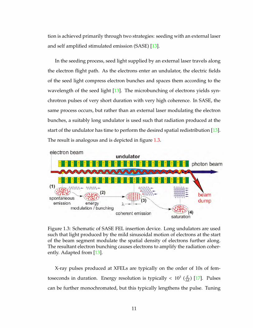
tion is achieved primarily through two strategies: seeding with an external laser
and self amplified stimulated emission (SASE) [13].
In the seeding process, seed light supplied by an external laser travels along
the electron flight path. As the electrons enter an undulator, the electric fields
of the seed light compress electron bunches and spaces them according to the
wavelength of the seed light [13]. The microbunching of electrons yields syn-
chrotron pulses of very short duration with very high coherence. In SASE, the
same process occurs, but rather than an external laser modulating the electron
bunches, a suitably long undulator is used such that radiation produced at the
start of the undulator has time to perform the desired spatial redistribution [13].
The result is analogous and is depicted in figure 1.3.
Figure 1.3: Schematic of SASE FEL insertion device. Long undulators are usedsuch that light produced by the mild sinusoidal motion of electrons at the startof the beam segment modulate the spatial density of electrons further along.The resultant electron bunching causes electrons to amplify the radiation coher-ently. Adapted from [13].
X-ray pulses produced at XFELs are typically on the order of 10s of fem-
toseconds in duration. Energy resolution is typically < 103 ( E∆E ) [17]. Pulses
can be further monochromated, but this typically lengthens the pulse. Tuning
11

of XFEL radiation energy is possible, but at present the process is more time
consuming than energy tuning at third generation sources. Pulse frequency is
limited by electron gun properties, but is currently being pushed upwards of
104 pulses/second on average [17].
In addition to average brilliance, peak brilliance is used as a metric to de-
scribe XFELs. Typical peak brilliance values seen at XFELs which have been
built or are being built reach upwards of 1033 photonssecond∗mrad2∗mm2∗0.1%BW . This tremen-
dous increase in brilliance, along with drastically reduced pulse duration, will
enable entirely new and exciting experiments.
1.2.2 X-ray detectors
There are numerous ways to detect and quantify an x-ray signal. This section
aims to provide a brief overview of the dominant architectures with two di-
mensional spatial resolution. Specifically, point and strip detectors (zero di-
mensional and one dimensional detectors, respectively) will not be discussed,
though they do find use in modern x-ray science. Area detectors all require
some sensing medium, which absorbs incident radiation to be measured, and
some means of quantifying the absorbed signal.
One distinction amongst x-ray detectors can be made with regard to the
means by which they convert radiation to a measurable signal: direct and in-
direct. Indirect conversion x-ray detectors use a sensing medium to convert x-
rays to an intermediate signal prior to conversion to the signal that is ultimately
measured. A prime example of indirect conversion detectors is the phosphor-
coupled charge coupled device.
12
Charge coupled devices, more commonly referred to as CCDs, find wide
use in optical imaging both in consumer and scientific markets. CCDs consist
of silicon doped in particular patterns such that light can be absorbed in the
camera’s pixels, and generated photo-charge is held in electric potential wells
in the pixels in which the radiation was absorbed. At the end of an imaging
period, a sequence of voltage changes can shuffle a column’s charge to the edge
of the sensor pixel-by-pixel to a readout amplifier which converts the integrated
charge to a voltage. While direct detection CCDs designed for infrared light and
x-rays have been constructed with thicknesses of hundreds of microns [18], the
pixel volume in which light can be absorbed and measured efficiently in most
CCDs is only a few microns [19]. The penetration depth of x-rays in silicon is
much longer than that of visible light, so CCDs designed for use with visible
light will only detect a small fraction of incident x-ray radiation. Most incident
x-rays will pass through the sensitive volume without depositing a measurable
signal. The absorption of photons in a semiconductor will be discussed further
in Chapter 2. To increase the fraction of x-rays which can be detected by a CCD,
the surface of the CCD can be coated with a scintillator or phosphor. Alterna-
tively, the scintillator can be placed on a fiber optic bundle that couples the light
to the CCD pixel array.
The phosphor absorbs x-rays and subsequently emits visible photons. These
photons can then be imaged by the optical CCD with much greater efficiency.
While CCDs can be manufactured with very low noise specifications, the phos-
phor intermediary introduces a number of undesirable effects in the data ob-
tained. For example, the light emitted by the phosphor is emitted isotropically,
so half of the signal is directed away from the imager. Additionally, the conver-
sion efficiency of the phosphor is less than one, and thus the signal to noise ratio
13

of the data will be reduced relative to an efficient direct detection implementa-
tion [19]. Furthermore, the location at which the radiation struck the phosphor
is more poorly defined, generally by a factor related to the thickness of the phos-
phor, as the emitted visible light undergoes a random walk through the phos-
phor prior to being detected by the CCD. These problems can be addressed to
some extent, but are common to all indirect sensing detectors. Some other cam-
era archetypes fall into the indirect detection category as well, including most
monolithic active pixel sensors, which employ a scintillating layer in x-ray ap-
plications for the same reason as CCDs [20].
As noted above however, direct detection CCDs are used in x-ray science,
and their development is ongoing [18, 21]. Film is also a direct detection tech-
nology, though it’s use has decreased as alternate means of quantifying x-ray
signals have matured. The detector architecture focused on in this dissertation
is the hybrid pixel array detector (PAD), also a direct detection technology. Hy-
brid PADs employ a dedicated sensing layer which electrically couples directly
to pixels. Chapter 2 contains a detailed discussion of the technology.
There is no universally optimal detector. The particular requirements of an
experiment will dictate which detectors are suitable. The following section
briefly outlines some common measures which can be used to evaluate and
compare detector performance.
Detector metrics
Various metrics exist for the comparison of x-ray detectors. Here we introduce
several parameters which will be relevant in later sections. A broad measure of
14
a detector’s limitations is the detective quantum efficiency (DQE) defined as
DQE =(S o/No)2
(S i/Oi)2 . (1.12)
S and N in Equation 1.12 refer to signal and noise respectively while the
subscript o refers to the output and i refers to the input. This is a measure of
the detector’s impact on the signal-to-noise ratio [22]. For example, if the sig-
nal being measured is x-rays subject to Poisson statistics, the input noise is the
square root of the number of incident x-rays. A DQE of 1 implies that the de-
tector perfectly measures the input signal without introducing any additional
noise or uncertainties. A real detector’s DQE is always less than one. DQE can
vary between individual measurements based on many parameters such as the
magnitude of the input, the spatial distribution of the input, the energy of pho-
tons which constitute the input, and more, but DQE can be used to compare the
performance of different detectors measuring the same signal. Factors which
affect a detector’s DQE can be examined independently.
As alluded to earlier, stopping power is the fraction of incident x-rays which
deposit their energy in the detector’s sensitive region. This is the metric which
indirect detection methods improve with phosphor coatings. Direct detection
methods also have a stopping power less than unity. Some fraction of incident
x-rays will not be absorbed, even by an ideal sensor. Transmission at normal
incidence of x-rays through a material of thickness d drops exponentially with
thickness as
T = e−nµad (1.13)
where n is the number of atoms per unit volume in the material and µa is the
atomic photoabsorption cross section [23]. As such, the absorption of x-rays in
the material is one minus this quantity. Other factors such as absorption of sig-
15
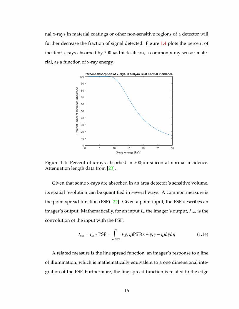
nal x-rays in material coatings or other non-sensitive regions of a detector will
further decrease the fraction of signal detected. Figure 1.4 plots the percent of
incident x-rays absorbed by 500µm thick silicon, a common x-ray sensor mate-
rial, as a function of x-ray energy.
Figure 1.4: Percent of x-rays absorbed in 500µm silicon at normal incidence.Attenuation length data from [23].
Given that some x-rays are absorbed in an area detector’s sensitive volume,
its spatial resolution can be quantified in several ways. A common measure is
the point spread function (PSF) [22]. Given a point input, the PSF describes an
imager’s output. Mathematically, for an input Iin the imager’s output, Iout, is the
convolution of the input with the PSF:
Iout = Iin ∗ PSF =
∫area
I(ξ, η)PSF(x − ξ, y − η)dξdη (1.14)
A related measure is the line spread function, an imager’s response to a line
of illumination, which is mathematically equivalent to a one dimensional inte-
gration of the PSF. Furthermore, the line spread function is related to the edge
16
spread function, an imager’s response to a step function input. The line spread
function is the derivative of the edge spread function [24].
The maximum signal that an imager can measure without saturation is the
full well, usually specified on a per-pixel basis. The dynamic range of an imager
describes the range of signal magnitudes which can be accurately measured.
What this means exactly can vary between imagers and applications. Often dy-
namic range is reported as a pixel’s full well divided by the read noise. For the
purposes of this work, we will consider two definitions. One is the single pulse
dynamic range. This is the range of signals measurable when the input arrives
within a time frame that is much faster than the detector’s response time. The
second is the continuous signal dynamic range. This is the range of continuous
signals which can be measured, generally expressed in units of x-rays per pixel
per second. Each parameter is relevant in different scenarios.
To understand this metric, we must ask what it means for a signal to be mea-
surable. In this work, the smallest signal of interest will be the signal from a
single x-ray. To resolve this signal with very few false positive or false negative
detections, one might require, for example, a signal to noise ratio of at least 5.
This indicates that, in the absence of actual signal, a one x-ray signal will be seen
due to noise less than once per one million measurements in a given pixel, as-
suming that pixel noise is Gaussian. Regarding the upper end of dynamic range,
x-ray signals are subject to shot noise, owing to the discreet nature of photons.
This means that measurements of photons are subject to Poisson statistics and
the inherent uncertainty in the determination of the average number of photons
which should arrive in a given time window is the square root of the number
17

of photons measured1. When measuring a large signal, this uncertainty is un-
avoidable. Noise is also added to the measurement by the detector. Because
these two noise sources are independent and uncorrelated they add in quadra-
ture [25]. In this work we aim to keep the uncertainty in a measurement due to
the detector smaller than the uncertainty due to Poisson statistics. Of course the
fractional uncertainty of a signal goes to zero as the mean signal goes to infinity.
Formally speaking, the upper end of dynamic range can be specified by when
uncertainty in a measurement is dominated by detector systematics. Practically
speaking, useful measurements can be made with uncertainties of a few tenths
of a percent for large signals.
1.3 Summary and document organization
X-rays are a powerful probe of materials that can provide information about the
organization and spacing of atoms in a sample. Obtaining this information re-
quires a suitable x-ray source and x-ray detector. Synchrotron radiation facilities
are a high brilliance source of x-rays. As synchrotron technology matures, the
list of its useful scientific applications continues to grow, but hurdles still exist
which prevent the full realization of these promising new techniques. Perhaps
most prominent among these challenges is the detector problem. In essence, x-
ray light source technology is out pacing x-ray detector technology. While x-ray
free electron lasers enable a wide range of experiments in theory, their full real-
1To understand this, imagine trying to measure the rate of cars passing a particular exit ona busy highway. You can count cars for one minute and you will measure an integer numberof cars because cars are discreet objects. If you were to repeat this measurement, you wouldprobably count a slightly different number of cars, just by chance. Some variation betweenmeasurements is expected. Measuring the number of x-rays that arrive at a detector withinsome time window, the integration time, yields variations described by Poisson statistics.
18

ization is hindered by a lack of suitable x-ray detectors [26, 27]. X-rays can be
diffracted, but the experimenter has poor means of adequately quantifying the
scattered x-rays.
The development of a high dynamic range pixel array detector, discussed
herein, aims to bridge the gap between synchrotron capabilities and x-ray detec-
tor capabilities. Chapter 2 discusses the technology of integrating hybrid pixel
array detectors and the complementary metal oxide semiconductor (CMOS)
technology that underlies their unique functionality. Chapter 3 discusses a par-
ticular application of integrating hybrid pixel array detector technology to illus-
trate the importance of high dynamic range. Chapter 4 discusses the conceptual
framework for the high dynamic range detector built in this work. Chapter 5
details the first pixel substructures built for this detector and their characteriza-
tion. Finally, chapters 6 and 7 discuss the 16x16 pixel x-ray detector constructed
with these pixels and discusses its performance.
19

CHAPTER 2
HYBRID PIXEL ARRAY DETECTORS
2.1 Introduction
Several varieties of x-ray detectors are in operation around the world. Of these
detectors, hybrid pixel array detectors (PADs) are arguably best suited to meet
the dynamic range requirements of modern synchrotron and x-ray FEL light
sources. This chapter contains an outline of PADs and an examination of the
technology and semiconductor physics which underlie their functionality. The
two primary archetypes of PADs, integrating and counting, will be discussed
and compared. Finally, two integrating pixel array detectors with state-of-the-
art dynamic range will be discussed, as the strategies they employ will be uti-
lized in this work.
2.1.1 PAD overview
A hybrid pixel array detector (PAD) module consists of three primary compo-
nents as depicted in Figure 2.1: the diode detection layer, the CMOS electronics
layer, and bump bond connections between the two. Additional off-chip elec-
tronics are wire bonded to the CMOS electronics layer to send data to and from
pixels, supply power, manage bias voltages and currents, and interface with the
chip in any other ways needed.
The diode detection layer, or simply the sensor, converts incident signal x-
rays into an electronic charge which is measurable by pixel-circuits contained in
20

Figure 2.1: A cartoon schematic of a hybrid pixel array detector. The CMOSelectronics layer is a lattice of pixel-circuits which measure signals coming fromthe diode detection layer. The diode detection layer converts incident radiationinto an electronic signal. The bump bonds connect the diode detection layer andCMOS electronics layer on a per-pixel basis, transferring electronic signals fromthe region of the detection layer in which radiation was absorbed to the nearestpixels. The image is adapted from [28] and is not to scale.
the CMOS electronics layer. The CMOS electronics layer, an application specific
integrated circuit (ASIC), is the heart of the detector. The ASIC is segmented
into pixels, and each pixel contains dedicated signal processing circuitry. Bump
bonds connect the two layers pixel-by-pixel such that charge generated in the
sensor flows into pixels in the ASIC. Charge carriers generated in the sensor will
typically enter the pixels nearest the sensor region in which they were gener-
ated. As a result, PADs perform spatially resolved imaging. The ASIC contains
additional, non-pixel circuitry to communicate with off-ship electronics.
To understand how these pieces function, some understanding of semicon-
ductor and CMOS device physics is necessary. The following section aims to
provide that foundation.
21

2.2 Semiconductor physics
The simplified discussion given here will be limited to monatomic crystalline
semiconductors, as their function is most relevant to this work. By this means
we will attempt to gain a qualitative understanding of the origins of some rel-
evant semiconductor properties. More in-depth reviews of semiconductors,
semiconductor physics, and CMOS device physics, can be found in many ex-
cellent textbooks [7, 29, 30].
2.2.1 Energy bands
Broadly speaking, materials can be categorized by their resistivity as insulators,
metals, or semiconductors. Other categories such as semi-metals can be defined,
but for the sake of simplicity we will limit discussion to the first three categories
mentioned. The resistivity of metals varies, but can be as low as 10−10 Ω-cm.
A strong insulator can have a resistivity as high as 1022 Ω-cm [7]. Throughout
the middle of this enormous range are materials called semiconductors. The
resistivity of semiconductors is generally temperature dependent. For example,
a semiconductor may insulate at low temperatures, but conduct reasonably well
at high temperatures. In contrast, many insulators will melt or sublime before
attaining an appreciable conductivity [31].
To understand the massive variation in resistivity seen throughout nature,
we must understand energy bands in crystalline materials. The possible ener-
gies of an electron bound to a lone atom are discreet. These are the so called
energy levels of a given element. Two atoms of the same element which are
22

far apart will each create an identical set of allowed electron states. If we bring
the two atoms close together, the degeneracy of their energy levels is broken
by splitting into two different but closely spaced energy levels [32]. A crystal
is composed of many atoms brought together in a lattice, and the result is the
splitting of energy levels into many separate states which, in the case of an in-
finite crystal, form a continuum called a band. The allowed electron states in a
crystal are therefore described by energy bands.
Alternatively, we can view electrons in a crystal as mostly free, but perturbed
by a periodic potential produced by the lattice of atomic nuclei. A free electron’s
momentum is described by a wave vector. In a periodic potential particular
wave vectors yield multiple solutions to the Schrodinger equation. Specifically,
two standing wave solutions with different energies exist for wave vectors com-
posed of a linear combination of reciprocal lattice vectors. In one solution that
standing wave is peaks between peaks in the potential, the lower energy solu-
tion, while the other features peaks which coincide with potential peaks, corre-
sponding to a higher energy state. These states are related to Bragg reflections
as discussed in Chapter 1, however the wave in this case is the electron’s po-
sition probability density function. The result is a gap between continuums of
allowed electron wave vectors in the presence of a periodic potential [7]. The
gaps between bands are known as band gaps.
To be slightly more concrete, figure 2.2 depicts the dispersion relation (en-
ergy as a function of wave vector ~k) for an electron in a one dimensional weak
sinusoidal potential with periodicity a. The dispersion relation for a completely
free electron (i.e. potential = 0 everywhere in space) is a parabola. Figure 2.2
differs from the free electron most notably at integer multiples of πa . At these
23
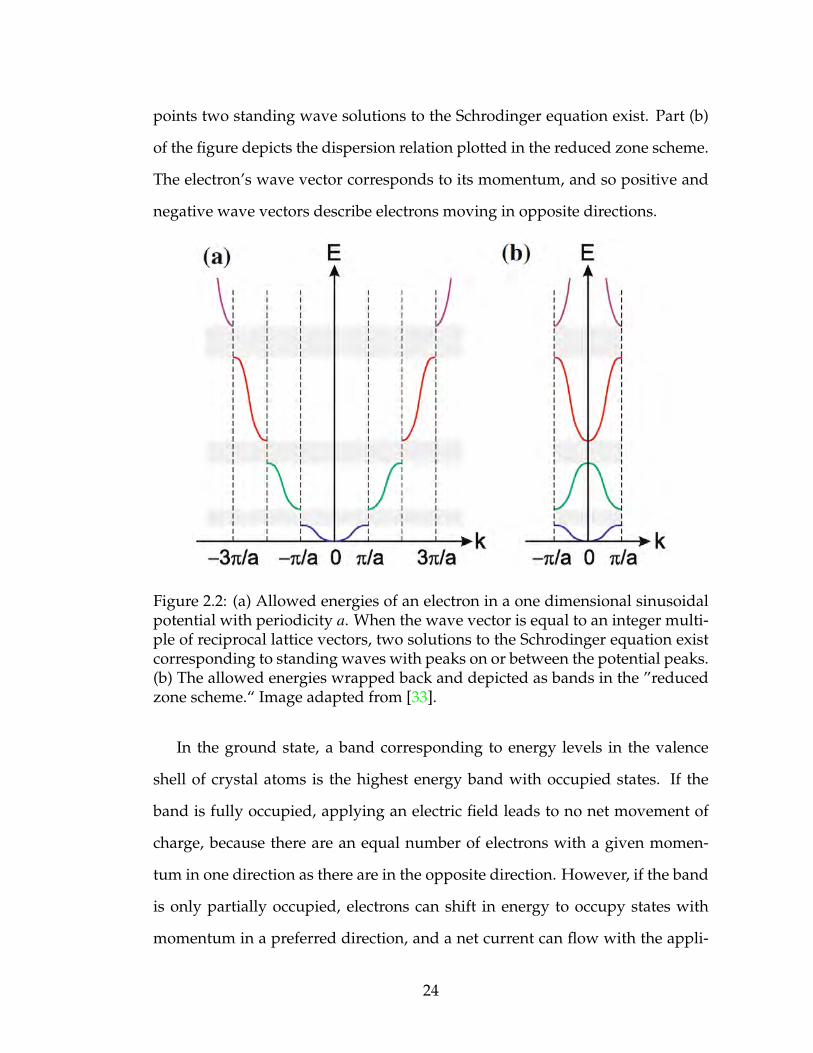
points two standing wave solutions to the Schrodinger equation exist. Part (b)
of the figure depicts the dispersion relation plotted in the reduced zone scheme.
The electron’s wave vector corresponds to its momentum, and so positive and
negative wave vectors describe electrons moving in opposite directions.
Figure 2.2: (a) Allowed energies of an electron in a one dimensional sinusoidalpotential with periodicity a. When the wave vector is equal to an integer multi-ple of reciprocal lattice vectors, two solutions to the Schrodinger equation existcorresponding to standing waves with peaks on or between the potential peaks.(b) The allowed energies wrapped back and depicted as bands in the ”reducedzone scheme.“ Image adapted from [33].
In the ground state, a band corresponding to energy levels in the valence
shell of crystal atoms is the highest energy band with occupied states. If the
band is fully occupied, applying an electric field leads to no net movement of
charge, because there are an equal number of electrons with a given momen-
tum in one direction as there are in the opposite direction. However, if the band
is only partially occupied, electrons can shift in energy to occupy states with
momentum in a preferred direction, and a net current can flow with the appli-
24

cation of an electric field. Metals have a valence band which is partially full and
thus conduct electricity. Insulators have a valence band which is completely
full, and thus they conduct poorly. However, allowed electron states exist in
bands with higher energy than the valence band. With sufficient energy an elec-
tron can move to an unoccupied band. If electrons from a fully occupied band
are excited into a higher energy band, the material becomes conductive. The
band above the valence band is called the conduction band. The band gap in
insulators is typically large relative to thermal energy. The band gap in semicon-
ductors is often comparable to the thermal energy (on the order of 1 eV). Higher
temperatures lead to greater occupancy of the conduction band in semiconduc-
tors. This explains why semiconductors conduct more at higher temperatures,
while insulators may melt before they gain an appreciable conductivity.
2.2.2 Doping semiconductors
From the band model we see that a material with a partially filled band con-
ducts electricity, while materials with only full and empty bands are insulators.
Materials with nearly full or nearly empty bands are weak conductors. With a
suitably small band gap, increasing temperature can alter band populations and
increase the conductivity of a semiconductor. An alternative means of increas-
ing the conductivity of a semiconductor is doping.
For a qualitative understanding of doping, consider a silicon crystal. Silicon
has four valence electrons and forms a diamond lattice, the silicon atoms each
bond covalently with their four nearest neighbors. Suppose that we replace one
silicon atom with one boron atom. Boron has three valence electrons, so it will
25
be able to fulfill three of the four bonds that are ordinarily made by atoms in the
diamond lattice.
Because the boron atom lacks an electron relative to the silicon atom it re-
places, one electron has been removed from the valence band of the crystal. An
electron could be paired with the neighboring, unpaired silicon electron, but in
a charge neutral material no electron is present for pairing. One could imagine
an electron from a nearby atom jumping over to fill this vacancy. The jumping
electron would of course leave behind its own vacancy, which could be filled by
another jumping electron, and so on. By replacing a silicon atom with a boron
atom we’ve added a hole to the valence band of the silicon crystal, and the hole
can now facilitate the net movement of charge.
Conversely, we might replace one silicon atom with one atom of phospho-
rus, which has five valence electrons. All four silicon bonds can be satisfied
in the diamond lattice, but the fifth valence electron of the phosphorus atom is
unpaired. The electron must still occupy a state defined by the band structure
of the crystal, and so the electron occupies a state in the conduction band. The
electron is free to move with an externally applied electric field, i.e. conduct
electricity. Figure 2.3 provides a cartoon depiction of the electron pairing in a
fictitious, two dimensional silicon square lattice with and without doping.
Note that the conducting charges in each doping case are opposite polarity.
When electron acceptors such as boron are added, the charge moving through
the crystal is positive. When electron donors are added, such as phosphorus, the
mobile charge is negative. Doped silicon is classified as n or p type, depending
on whether the dopant is an electron donor or acceptor, respectively. This pro-
cess is of course more complicated than presented above. For example, dopants
26
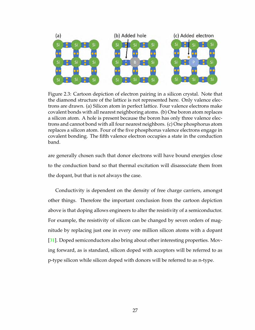
Figure 2.3: Cartoon depiction of electron pairing in a silicon crystal. Note thatthe diamond structure of the lattice is not represented here. Only valence elec-trons are drawn. (a) Silicon atom in perfect lattice. Four valence electrons makecovalent bonds with all nearest neighboring atoms. (b) One boron atom replacesa silicon atom. A hole is present because the boron has only three valence elec-trons and cannot bond with all four nearest neighbors. (c) One phosphorus atomreplaces a silicon atom. Four of the five phosphorus valence electrons engage incovalent bonding. The fifth valence electron occupies a state in the conductionband.
are generally chosen such that donor electrons will have bound energies close
to the conduction band so that thermal excitation will disassociate them from
the dopant, but that is not always the case.
Conductivity is dependent on the density of free charge carriers, amongst
other things. Therefore the important conclusion from the cartoon depiction
above is that doping allows engineers to alter the resistivity of a semiconductor.
For example, the resistivity of silicon can be changed by seven orders of mag-
nitude by replacing just one in every one million silicon atoms with a dopant
[31]. Doped semiconductors also bring about other interesting properties. Mov-
ing forward, as is standard, silicon doped with acceptors will be referred to as
p-type silicon while silicon doped with donors will be referred to as n-type.
27
2.2.3 P-n junctions
Consider two adjacent regions of a doped semiconductor, one doped with
donors and the other with acceptors. Charge carriers from each region will dif-
fuse into the other and electrons from donor dopants will fill the vacancies from
acceptor dopants. Now the regions on either side of the boundary will possess
a net electric charge. Donor dopant atoms which have lost their 5th valance
electron now have a net positive charge and acceptor dopant atoms which have
accepted a fourth valence electron now have a net negative charge. As a re-
sult, an electric field is established across the junction. This field counteracts
free charge carrier diffusion, sweeping charge carriers away from the junction
and establishing an equilibrium condition. The region that is devoid of mobile
charge carriers is called the depletion region.
This p-n junction is a diode. Consider the effects of applying a bias volt-
age across the device. If the n-doped side of the junction is brought to a higher
voltage than the p-doped region, the applied bias serves to widen the deple-
tion region by pulling electrons in the n-doped region away from the junction
and pushing holes in the p-doped region away from the junction. The depleted
region will grow until the charge of atoms in the region form an electric field
strong enough to reach an equilibrium with the externally applied bias. After a
brief flow of current out of the diode, no more current flows due to the externally
applied voltage. The junction is reverse biased. If we increase the applied bias
high enough, electrons receive enough energy from the electric field to jump
from the valence band to the conduction band. This is Zener breakdown [29].
Additionally, avalanche breakdown can occur when applied electric fields are
strong enough that accelerated charge carriers create electron-hole pairs when
28

they collide with atoms in the lattice. However, our discussions will not concern
these regions of operation.
If enough of the opposite bias is applied, such that the p-doped region is
brought to a higher voltage than the n-doped region, each side’s respective
charge carriers will be pushed towards the junction. Opposite charge carri-
ers from either side will combine and nullify. Here we see that current flows
relatively freely. In this case the diode is forward biased.
2.2.4 Radiation in a reverse biased diode
Now return to the case of reverse biasing. Suppose we supply a large enough
voltage to deplete the bulk of the semiconductor. In a fully depleted diode the
current drawn will be primarily due to thermally excited electron hole pairs
generated in the depletion region and swept out by the diode’s internal electric
field. This is the so-called “dark current.” The magnitude of dark current falls
off exponentially with temperature as [34]
I ∝ T 2exp(−
Eg
2kBT
)(2.1)
where I is the dark current, T is temperature, Eg is the semiconductor’s band
gap energy, and kB is the Boltzmann constant. Impurities in the semiconductor
material exacerbate the dark current, as the impurities can provide energy levels
accessible to valence band charge carriers that are intermediate to the valence
band and the conduction band. These “stepping stones” allow smaller thermal
excitations to eventually bring electrons to the conduction band.
If a high energy photon is absorbed in a reverse biased diode, the energy
29

deposited creates a cloud of electron-hole pairs. In silicon, roughly 3.6eV is re-
quired to create an electron-hole pair. When a single x-ray with an energy of 8
keV is absorbed in a silicon diode, more than two thousand electron hole pairs
are created. The exact number of pairs will vary slightly between absorption
events, but note that the distribution of the number of electron-hole pairs cre-
ated is not Poissonian because the creation of each electron-hole pair is not an
independent random event. Rather, the events are correlated and because of the
finite number of channels for the x-ray energy to enter, the standard deviation
of the number of electron-hole pairs created is only a fraction of the square root
of the mean. This fraction is called the Fano factor and equals 0.1 in silicon.
The electron-hole pairs generated form a small cloud [29]. The electric field
inside the diode will separate the electrons from the holes and pull them to
separate terminals. Figure 2.4 is a cartoon depiction of a reverse biased diode
which forms the sensor of a pixel array detector. As the clouds drift through
the diode, the cloud expands due to diffusion. More will be said about this in
Chapter 4. Some electrons and holes will recombine before separation by the
electric field. The rate at which this occurs is the carrier lifetime. In silicon,
this lifetime is surprisingly long as a result of silicon being an indirect band gap
material, but is often facilitated by impurities and lattice defects. More can be
found on the topic in, for example, [35].
Ultimately, a reverse biased diode can serve as a sensor for radiation: pho-
tons are absorbed and an electric current flows out of the diode in proportion
to the energy of the absorbed radiation. While the specifications of x-ray PAD
sensors vary, along with the material used, the detectors in this work utilize 500
microns thick Si photodiode sensors.
30
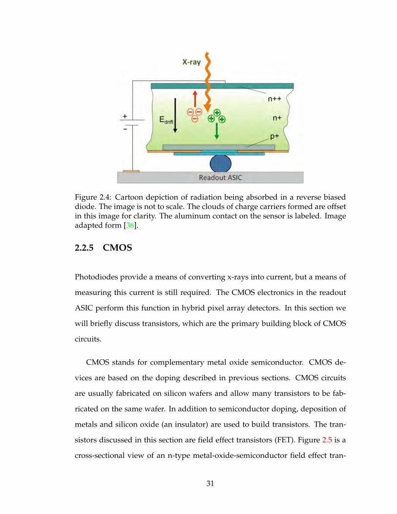
Figure 2.4: Cartoon depiction of radiation being absorbed in a reverse biaseddiode. The image is not to scale. The clouds of charge carriers formed are offsetin this image for clarity. The aluminum contact on the sensor is labeled. Imageadapted form [36].
2.2.5 CMOS
Photodiodes provide a means of converting x-rays into current, but a means of
measuring this current is still required. The CMOS electronics in the readout
ASIC perform this function in hybrid pixel array detectors. In this section we
will briefly discuss transistors, which are the primary building block of CMOS
circuits.
CMOS stands for complementary metal oxide semiconductor. CMOS de-
vices are based on the doping described in previous sections. CMOS circuits
are usually fabricated on silicon wafers and allow many transistors to be fab-
ricated on the same wafer. In addition to semiconductor doping, deposition of
metals and silicon oxide (an insulator) are used to build transistors. The tran-
sistors discussed in this section are field effect transistors (FET). Figure 2.5 is a
cross-sectional view of an n-type metal-oxide-semiconductor field effect tran-
31

sistor (MOSFET). The transistor is fabricated on a p-type substrate. The device
has four terminals (the substrate itself is the fourth terminal, but an explicit sub-
strate connection is not shown here). P-type MOSFETs can be constructed on the
same wafer as n-type MOSFETs, but they must be fabricated in a region which
is heavily n-doped to form a local n-type well, effectively setting the device in
an n-type substrate, and must be biased appropriately. N-type MOSFETs on p-
type wafers will be discussed below, but the results apply to both types with
appropriate changes in voltage sign and charge carrier species.
Figure 2.5: N-type MOSFET transistor cross-section. The four transistor termi-nals are the source, drain, gate, and substrate. Width and length (W and L re-spectively) describe the dimensions of the conductive channel formed beneaththe gate when inverted. Image adapted from [37] with alterations.
Note that the transistor in figure 2.5 is physically symmetric about the gate.
For this reason, which terminal serves as the source and which terminal serves
as the drain depends on bias conditions. The source and drain terminals are
each heavily n-doped regions. Usually the substrate is tied to the lowest sys-
tem voltage. For our purposes, we will assume that the chip has only a positive
supply, and so the substrate is tied to ground. It can be seen based on the anal-
ysis of n-p junctions above that the source to substrate and drain to substrate
32

are diode junctions which will never be forward biased if the substrate remains
at ground. The gate terminal is usually composed of metal or a highly doped
polycrystalline silicon [38] and is separated from the substrate by a thin insulat-
ing layer. If the gate is held at ground and a bias is applied between the source
and drain terminals, the n-p-n segment beneath the gate cannot conduct elec-
tricity in either direction because one of the n-p junctions will always be reverse
biased.
A capacitance is formed between the gate and substrate which is propor-
tional to the product of the length and width of the transistor gate as depicted
in figure 2.5. By applying a positive voltage to the gate of the transistor, holes
(the majority charge carrier in the substrate) are repelled. A depletion region
forms beneath the gate and the electric potential of the substrate at the silicon-
silicon oxide interface rises [30]. If the gate bias is increased further, the energy
level of the conduction band at the silicon oxide interface approaches the Fermi
level of electrons in the substrate [37]. Eventually the conduction band at this
interface is populated by electrons and current can flow between the source and
drain. When the electron density in this channel is equal to the native hole den-
sity of the doped substrate the transistor is said to be inverted: electrons are
now the dominant charge carrier at the interface. Note that the ”turning on“ of
a transistor is a gradual process. For the sake of disambiguation, an ”on“ volt-
age is defined, generally as the gate voltage sufficient to invert the channel, and
is referred to as the transistor threshold voltage (Vth).
More formally, for an n-type MOSFET the electric potential of the channel,
ψs, when mobile electron concentration equals the dopant concentration must
33

be
ψs = 2ΦF (2.2)
relative to ground defined by the substrate very far from the channel, where
ΦF is the potential of the bulk in depletion due to positively charged acceptor
atoms which is equivalent to the Fermi level of the unbiased substrate minus
the Fermi level of the depleted substrate. From Boltzmann statistics we have
ΦF =kBT
eln
Na
ni(2.3)
where kB is the Boltzmann constant, T is temperature, e is the electron charge,
Na is the density of doped acceptor atoms, and ni is the intrinsic density of
charge carriers in the unbiased semiconductor [37]. The gate voltage required
to achieve inversion is the threshold voltage:
Vth = ΦMS + 2ΦF +Qdep
Cox, (2.4)
where ΦMS is the difference in work function between the gate material and the
substrate, Cox is the gate oxide capacitance per unit area, and Qdep is the charge
in the depletion region,
Qdep =√
4εsieNa|ΦF | (2.5)
where εsi is the dielectric constant of the substrate (silicon) [30].
We can analyze the current flow between the source and drain when the
channel is inverted. Note that the source is the source of charge carriers conduct-
ing through the device. In the case of an n-type transistor the charge carriers are
electrons. For gate voltages beyond Vth, charge in the channel will mirror charge
across the oxide capacitance on the gate. Assuming that the source voltage is
held at ground and Vgs ≥ Vth where Vgs is the voltage difference between the
gate and the source, following the derivation in [30], the charge in the channel
34

per unit length is
Qd = WCox(Vgs − Vth), (2.6)
where W is the width of the transistor channel. If the voltage between the drain
and source, Vds, is greater than zero, the potential throughout the channel will
not be uniform, and the charge density will not be either. The charge per unit
length in the channel a distance x from the source will be
Qd(x) = WCox[Vgs − V(x) − Vth], (2.7)
where V(x) is the potential in the channel as a function of x. In semiconductors,
the mean carrier velocity is v = µE where µ is the charge mobility and E is the
electric field [30], so the current in the channel is
Ids(x) = WCox[Vgs − V(x) − Vth]µndV(x)
dx, (2.8)
noting that µn is the electron mobility in silicon and E = − dVdx . The minus sign in
the equation for current is lost because the charge carriers have negative charge,
therefore positive current flows in the direction opposite their velocity. Now
separating variables and integrating we have∫ x=L
x=0Id(x)dx =
∫ V=Vds
V=0WµnCox[Vgs − V(x) − Vth]dV (2.9)
which, assuming the biases meet saturation criteria, yields current through the
channel:
Id = µnCoxWL
[(Vgs − Vth
)Vds −
12
V2ds
]. (2.10)
For a given Vgs the current as a function of Vds is a convex parabola. The maxi-
mum current occurs when Vds = Vgs − Vth and is
Id,max =12µnCox
WL
(Vgs − Vth
)2. (2.11)
Vgs − Vth is called the overdrive voltage. If Vds ≤ Vgs − Vth the transistor is said to
be operating in the triode region.
35

As mentioned above, transistors do conduct when Vgs < Vth and the channel
is not yet completely inverted. A full derivation of sub-threshold operation is
beyond the scope of this work, but excellent treatments of the topic can be found
in textbooks such as [37, 38]. The transistor is a core building block with which
integrated circuits are constructed, including the ASICs of pixel array detectors.
2.2.6 Radiation hardened components
Radiation damage is an inevitable part of x-ray detector operation. Measures
can be taken to minimize the exposure of integrated circuits to radiation, but the
issue must always be addressed. Radiation damage in CMOS typically occurs
in two forms: displacement damage and ionization damage [34].
Displacement damage occurs when silicon atoms are displaced by radiation.
The altering of the silicon lattice leads to altered electrical properties of the ma-
terial. X-rays do not cause direct displacement damage, as the process requires
significant momentum transfer. The damage can be caused by Compton scat-
tering of highly energetic photons, but it is a far less prominent mechanism
of radiation damage in x-ray detectors, so this section will focus on ionization
damage.
Ionization damage is most evident in the ionization of silicon oxide. Ioniza-
tion of oxide is problematic because the carrier mobility of electrons and holes
in oxide are vastly different. As a result, if an electron is liberated in oxide, it
will often leave the material, never to recombine with its hole. Holes will un-
dergo some migration, depending on the applied electric fields, but they are far
more prone to trapping in the oxide. This leaves the oxide with an undesired,
36
long-term positive charge, which creates parasitic electric fields. This can have
a range of effects depending on what the oxide in question is used for. Ioniza-
tion in conductive materials is not damaging because both charge carriers can
be neutralized.
In reference to figure 2.5, conduction through the FET is regulated by the
voltage on the gate, labeled G. Conduction is inhibited by the opposite doping
of the source (S)/drain (D) and the channel/bulk. These nodes cannot con-
duct unless properly biased. When a positive voltage is applied to the gate of
an NMOS transistor, electrons form a channel beneath the gate connecting the
drain and source which allows current to flow through the transistor when a
drain-to-source voltage is applied.
Ionization damage in the oxide separating the gate from the bulk leads to
holes trapped near the oxide-bulk interface. The effect of these holes on the
formation of a channel in the FET is the same as a positive voltage being ap-
plied to the gate. In essence, ionization damage in FET oxides reduces the gate
voltage required to operate the FET. In extreme cases, it could cause a transistor
to remain permanently “on.” These trapped holes can be neutralized, for ex-
ample through tunneling of electrons from the bulk into the oxide. Changes in
threshold voltages for FETs due to ionization damage are typically on the order
of 100-200mV [39]. Thinner oxides are less prone to long-term ionization dam-
age because the probability of electrons tunneling through to trapped holes is
greater at shorter distances, and the ability of holes to migrate out of the oxide
is greater for thinner oxides. Ultimately, radiation damage can cause leakage
current issues in NFETs, degrading the ability of switches to full open and pre-
vent, for example, voltages sampled on capacitors from drifting. Quantitative
37

analysis of the impact of radiation damage is entirely dependent on the circuit
in question. For instance, it is possible that in some cases radiation damage in
more than one part of a circuit can lead to canceling effects. Ultimately, radiation
damage causes circuits to function in ways they were not intended to.
Depending on the complexity of the diode detection layer structures, radi-
ation damage can have a significant impact there as well. Insulators are used
to prevent leakage current in ring structures around the perimeter of large area
diodes used as sensors. High voltages applied to thin diodes (hundreds of volts
across a diode that is less than a millimeter thick in many cases) must be pre-
vented from conducting on diode edges. Oxide guard ring structures are often
used to segregate regions of varying voltages, and ionization damage can com-
promise this insulation. This leads to increased dark current.
Further, diodes in PADs typically use some oxide patterning to isolate elec-
trodes of adjacent pixels. Ionization of this oxide could lead to long term charge
at the oxide-silicon boundary. As with the NFETs discussed above, this has
the potential to form conductive electron channels linking adjacent pixels’ elec-
trodes. This would obviously have a detrimental effect on the detector’s spatial
resolution, as charge being collected in one pixel could easily leak to an adja-
cent pixel. As a result of this potential for radiation damage, holes are often
collected in PADs [40]. Here, positive charge in the oxide actually reinforces the
insulating properties of the structure, inhibiting the conduction of holes.
A variety of circuit design, fabrication, and layout techniques have been con-
ceived to produce circuits whose performance is less susceptible to degradation
due to radiation damage [39]. As device scaling moves to smaller and smaller
feature sizes, the long-term impact of radiation damage is mitigated because
38
charges trapped in oxide can more readily tunnel out. Even so, it is useful to
design circuits whose operation is robust in the face of heavy irradiation.
Designing a radiation hard circuit involves considering what circuit features
are most susceptible to radiation damage. For example, in the design of the
MM-PAD (a detector discussed in some depth below) pixel integrators, it was
noted that bias currents are used to set the functionality of the amplifier. As a
result of radiation damage to the bias network, or to biasing transistors in the
amplifier, gate voltages associated with given bias currents could be altered.
For this reason, it was important to make the function of the amplifier relatively
insensitive to bias current variations within a range that could be expected to
result from radiation damage.
Several steps have been identified in the device fabrication process which
can reduce the susceptibility of a circuit to radiation damage. For example,
hydrogen at the silicon-silicon oxide boundary of FETs serves to increase the
trapping of holes at the interface, which is detrimental to the function of FETs,
as discussed above. Annealing of intermediate circuits in pure nitrogen at spe-
cific temperatures has been found to decrease the amount of hydrogen trapped
at the boundary, and thus reduce the detrimental impact of radiation on CMOS
circuits fabricated in this way. At the layout level, many design structure, which
often come with an increased area cost, have been implemented to produce
more radiation hardened circuits. Incorporation of p-doped silicon guard struc-
ture to reduce thickness of oxides required in some circuit structures is one ex-
ample of these techniques [39].
39
2.3 Pixel array detectors
In this section we present a brief overview of pixel array detectors followed by
a discussion of the two dominant pixel architectures with which PAD ASICs are
built: counting and integrating.
As depicted in figure 2.1, hybrid PADs consist of two distinct layers, a ded-
icated sensing layer and a signal processing layer. To provide a sense of scale,
figure 2.6 is a photograph of a hybridized sensor wire bonded to support elec-
tronics. Figure 2.7 is a photograph of the an unhybridized PAD ASIC. The de-
tector depicted in figure 2.6 is the CS-PAD [41]. The detector depicted in figure
2.7 is the MM-PAD. It is a 128x128 pixel array with 150µm pixel pitch and a
500µm thick silicon sensor.
As discussed above, the sensing layer of a PAD is typically a monolithic pho-
todiode which is reverse biased and functions as described above. The sensing
layer is connected to the signal processing layer pixel-by-pixel via bump bonds.
Charge generated via x-ray absorption in the sensor is transferred to the pixi-
lated, signal processing ASIC. The diode is biased to create electric field lines
perpendicular to the p-n junction with the aim of sweeping photo-generated
charge from the point of absorption directly to the pixels corresponding to that
volume. Some patterning on the back side of the sensor is required to facilitate
the bonding of the ASIC and reduce cross-talk between pixels.
The ASIC contains an array of pixel-circuits. Each pixel contains its own sig-
nal processing circuitry which can function in a number of ways. Below we will
discuss two dominant pixel architectures employed in hybrid PADs for measur-
ing x-ray signals.
40
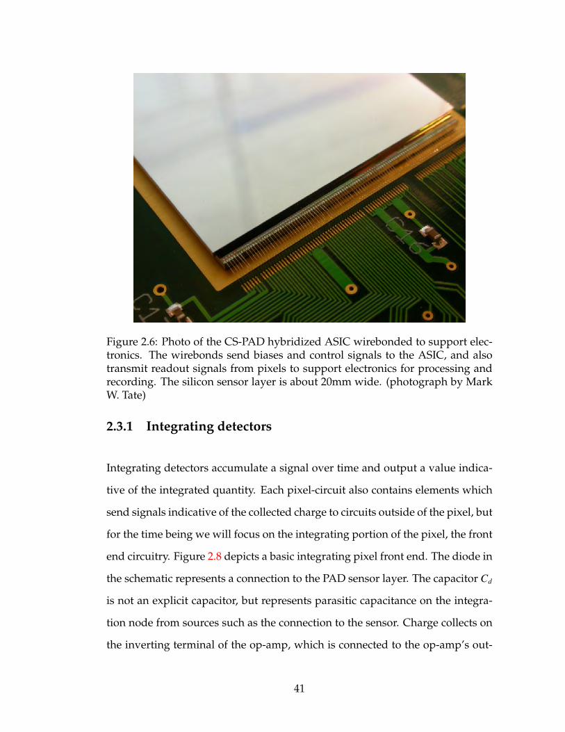
Figure 2.6: Photo of the CS-PAD hybridized ASIC wirebonded to support elec-tronics. The wirebonds send biases and control signals to the ASIC, and alsotransmit readout signals from pixels to support electronics for processing andrecording. The silicon sensor layer is about 20mm wide. (photograph by MarkW. Tate)
2.3.1 Integrating detectors
Integrating detectors accumulate a signal over time and output a value indica-
tive of the integrated quantity. Each pixel-circuit also contains elements which
send signals indicative of the collected charge to circuits outside of the pixel, but
for the time being we will focus on the integrating portion of the pixel, the front
end circuitry. Figure 2.8 depicts a basic integrating pixel front end. The diode in
the schematic represents a connection to the PAD sensor layer. The capacitor Cd
is not an explicit capacitor, but represents parasitic capacitance on the integra-
tion node from sources such as the connection to the sensor. Charge collects on
the inverting terminal of the op-amp, which is connected to the op-amp’s out-
41
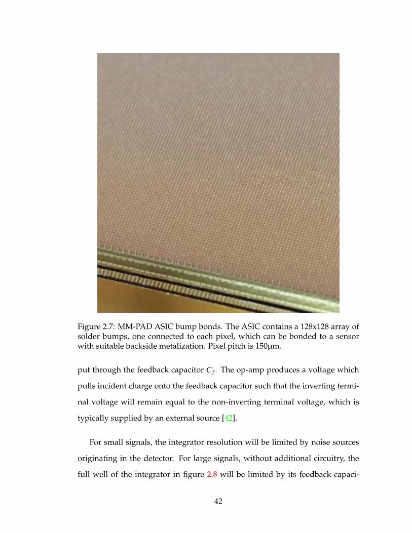
Figure 2.7: MM-PAD ASIC bump bonds. The ASIC contains a 128x128 array ofsolder bumps, one connected to each pixel, which can be bonded to a sensorwith suitable backside metalization. Pixel pitch is 150µm.
put through the feedback capacitor C f . The op-amp produces a voltage which
pulls incident charge onto the feedback capacitor such that the inverting termi-
nal voltage will remain equal to the non-inverting terminal voltage, which is
typically supplied by an external source [42].
For small signals, the integrator resolution will be limited by noise sources
originating in the detector. For large signals, without additional circuitry, the
full well of the integrator in figure 2.8 will be limited by its feedback capaci-
42

Figure 2.8: Basic integrating pixel schematic. The diode represents a connectionto the photodiode sensor. The amplifier collects charge incident from the photo-diode onto C f . Cd is not a real capacitor, but represents the parasitic capacitanceon the front end of the pixel. Vout is the pixel output, typically digitized outsideof the pixel through an analog transmission chain (not shown).
tance and operating voltages. A larger capacitor will allow charge generated by
a larger number of x-rays to be collected, but this impacts the small signal sen-
sitivity of the integrator. Increasing the capacitance reduces the gain of the inte-
grator and increases the equivalent noise charge due to noise sources internal to
the amplifier [43]. Therefore, to maintain single photon sensitivity, a sufficiently
small capacitor must be used. To better understand these limitations, the basic
operation of an integrating pixel is derived below.
Integrator properties
Assume that the amplifier in figure 2.8 is an ideal op-amp with infinite input
impedance and large gain A. The output voltage of the amplifier is
Vout = A(Vre f − Vin). (2.12)
43

If positive charge Qin enters the integration node through the photodiode, Vin in-
creases and Vout decreases. As a result, the voltage across the feedback capacitor
increases to
∆V f = Vin − Vout = Vin − A(Vre f − Vin). (2.13)
Assuming for the time being that the parasitic capacitance Cd is small, all charge
must be pulled onto the feedback capacitance because the input impedance of
the amplifier is infinite, so
Q f = C f ∆V f = Qin. (2.14)
The charge to voltage gain of this configuration is then
Vout
Qin=
A(Vre f − Vin)C f (Vin − A(Vre f − Vin))
≈−1C f
(2.15)
for large A. Therefore the output of the integrator in relation to the input charge
is approximately determined by the feedback capacitance.
Of course, this initial derivation neglects several important details. To un-
derstand the interaction between C f and Cd, we can view C f as a capacitor con-
nected in parallel to Cd with a capacitance enhanced by the dynamic response
of the backside voltage, the so called Miller effect [34]. In this way, the effective
capacitance on the front end due to C f is
Ce f f = C f (A + 1). (2.16)
The input charge is distributed between the two capacitors, C f and Cd. The
fraction of charge deposited on C f , which is the quantity being measured, is
Q f
Qin=
Ce f f
Ce f f + Cd, (2.17)
which is approximately one for large gain or small Cd. This emphasizes the im-
portance of a high gain integrating amplifier and illustrates that parasitic capac-
itance on the pixel front end degrades the integrator charge collection efficiency.
44

2.3.2 Amplifier noise in feedback
As noted above, the small signal resolution of an integrating pixel array detec-
tor is limited by the noise performance of the charge sensitive pre-amplifier (the
integrator). Output referred noise from the amplifier sees a capacitive voltage
divider formed by the feedback capacitor and the front end parasitic capaci-
tance. As a result, the output referred noise of the integrator shows up on the
input as [44]
Vin = VoutXCd
XC f + XCd
(2.18)
which simplifies to
Vout = Vin
(1 +
Cd
C f
)(2.19)
where Vin is the noise on the input as a result of the output referred noise being
fed back, Vout is the output referred noise, XCd and XC f are the reactance of the
front end parasitic capacitance and the feedback capacitance respectively, and
Cd and C f are those capacitances. The equivalent input noise charge, the amount
of integrated charge that the noise is interpreted as, is then
Qnoise−in = VoutC f = Vin
(Cd + C f
)(2.20)
which yields a signal to noise ratio of
Qs
Qnoise−in=
Qs
Vin
(Cd + C f
) (2.21)
where Qs is the charge signal you hope to measure, subject to the charge col-
lection efficiency derived in the previous section. Based on the analysis above,
we can design amplifiers with acceptable noise characteristics. Acceptable is of
course a subjective term, so design goals must be set. For example, it is com-
monly desirable in x-ray PADs to achieve good single x-ray sensitivity. It can
then be decided that the average integrated noise power of the amplifier must
45

yield a signal to noise ratio of at least 5 for the signal from a single 10keV x-
ray. Given amplifier noise characteristics and expected parasitic capacitances, a
maximum integration capacitance can be chosen. Conversely, a desired full well
might dictate the integration capacitance, and an amplifier with sufficiently low
noise can then be designed.
Calculation of the noise signal from a specific amplifier involves modeling
the noise of each component in the circuit, and propagating its effect through
the rest of the circuit. For example, if a transistor gate forms the input of an
amplifier, the noise generated by that transistor, modeled as an input voltage
noise source, results in the initial input noise power multiplied by the entire
amplifier’s gain. Noise from other transistors within the amplifier may have
less of an impact on the amplifier’s total noise. The bandwidth of the system
also regulates the impact of noise sources. When examining an amplifier for
noise consideration, it is also important to look at the amplifier’s susceptibility
to external noise sources, such as power supply ripple.
2.3.3 Electronic noise
Amplifier noise is a complicated subject and highly dependent on the specific
amplifier in question. An examination of general noise considerations will be
given here which is applicable to all amplifiers. While the discussion of noise
in feedback above dealt with output referred noise for the purpose of analysis
(that is the combination of all noise sources inherent to the amplifier), the source
of noise in amplifiers is typically internal to the device. Two forms of noise are
present in all circuits, namely Johnson noise and flicker noise, or 1/ f noise [42].
46

Johnson noise, also referred to as thermal noise, arises from random, thermal
motion of charge carriers in circuit elements. Take a simple resistor as an exam-
ple. The charge carriers in the resistor undergo random thermal motion, and
at any given moment we can expect to find a different number of electrons on
either end of the resistor. Even if the resistor is not connected to a circuit of any
kind, the free charge carriers in the resistor will be in motion. The time average
of the charge carriers’ velocities is zero, but at any given moment there may be a
non-zero voltage across the resistor due to charge imbalance. This phenomena
is the source of thermal noise in circuits. We find that the noise power spectral
density associated with Johnson noise is [42]
V2n = 4kBTR (2.22)
where kB is the Boltzmann constant, T is the temperature of the resistor, and R is
its resistance. For field effect transistors, the power spectral density of thermal
noise is [30]
V2n =
8kBT3
gm (2.23)
where gm is the transconductance of the transistor. Johnson noise is present in
any circuit element with finite resistance and its power spectrum is white. In
equation 2.22, equation 2.23, and all following equations in this section, power
spectral density is being referenced, and each equations is implicitly in watts per
hertz (W/Hz). The noise is subject to filtering effects of the circuit in question, and
the total noise power manifested is the integral over frequency of the relevant
noise quantity (e.g. equation 2.22 for a purely resistive network) multiplied by
the transfer function of the effective filter.
Flicker noise is also pervasive and arises from trapping of charge carriers in
materials. Often this trapping occurs at material boundaries such as field effect
47
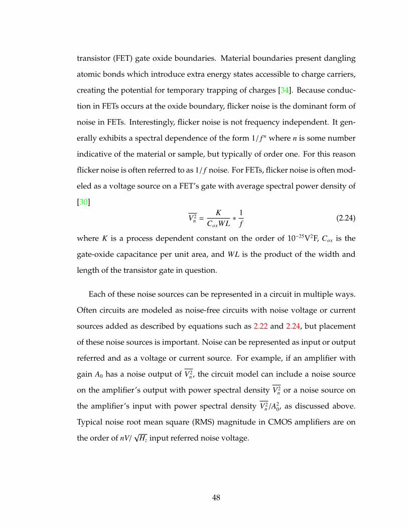
transistor (FET) gate oxide boundaries. Material boundaries present dangling
atomic bonds which introduce extra energy states accessible to charge carriers,
creating the potential for temporary trapping of charges [34]. Because conduc-
tion in FETs occurs at the oxide boundary, flicker noise is the dominant form of
noise in FETs. Interestingly, flicker noise is not frequency independent. It gen-
erally exhibits a spectral dependence of the form 1/ f n where n is some number
indicative of the material or sample, but typically of order one. For this reason
flicker noise is often referred to as 1/ f noise. For FETs, flicker noise is often mod-
eled as a voltage source on a FET’s gate with average spectral power density of
[30]
V2n =
KCoxWL
∗1f
(2.24)
where K is a process dependent constant on the order of 10−25V2F, Cox is the
gate-oxide capacitance per unit area, and WL is the product of the width and
length of the transistor gate in question.
Each of these noise sources can be represented in a circuit in multiple ways.
Often circuits are modeled as noise-free circuits with noise voltage or current
sources added as described by equations such as 2.22 and 2.24, but placement
of these noise sources is important. Noise can be represented as input or output
referred and as a voltage or current source. For example, if an amplifier with
gain A0 has a noise output of V2n , the circuit model can include a noise source
on the amplifier’s output with power spectral density V2n or a noise source on
the amplifier’s input with power spectral density V2n/A
20, as discussed above.
Typical noise root mean square (RMS) magnitude in CMOS amplifiers are on
the order of nV/√
Hz input referred noise voltage.
48
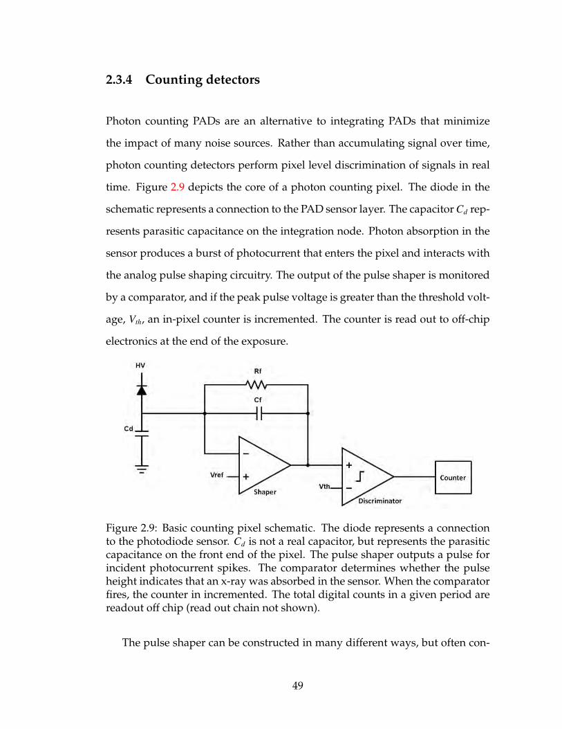
2.3.4 Counting detectors
Photon counting PADs are an alternative to integrating PADs that minimize
the impact of many noise sources. Rather than accumulating signal over time,
photon counting detectors perform pixel level discrimination of signals in real
time. Figure 2.9 depicts the core of a photon counting pixel. The diode in the
schematic represents a connection to the PAD sensor layer. The capacitor Cd rep-
resents parasitic capacitance on the integration node. Photon absorption in the
sensor produces a burst of photocurrent that enters the pixel and interacts with
the analog pulse shaping circuitry. The output of the pulse shaper is monitored
by a comparator, and if the peak pulse voltage is greater than the threshold volt-
age, Vth, an in-pixel counter is incremented. The counter is read out to off-chip
electronics at the end of the exposure.
Figure 2.9: Basic counting pixel schematic. The diode represents a connectionto the photodiode sensor. Cd is not a real capacitor, but represents the parasiticcapacitance on the front end of the pixel. The pulse shaper outputs a pulse forincident photocurrent spikes. The comparator determines whether the pulseheight indicates that an x-ray was absorbed in the sensor. When the comparatorfires, the counter in incremented. The total digital counts in a given period arereadout off chip (read out chain not shown).
The pulse shaper can be constructed in many different ways, but often con-
49
sists of an integrating amplifier with a DC feedback element, such as a resis-
tor, to prevent signal from persisting on the integration capacitance [45]. The
threshold Vth can be set such that only x-rays with sufficient energy will trigger
the comparator and thus increment the counter. This has several advantages
and disadvantages which will be discussed in the next section. amplifier noise
on the front end amplifier and power supply or reference voltage fluctuations,
along with the pulse shaper properties, set the minimum photon signal which
can be recorded.
By performing an analog to digital conversion at the pixel level, full well is
no longer limited by a capacitor size, but instead the depth of a digital counter.
This extends the full well drastically.
2.3.5 Comparing integrating pixels and counting pixels
By identifying individual photon events, counting detectors (with proper cali-
bration, which can be difficult) are able to ignore dark current entirely. In con-
trast, integrating detectors accumulate dark current, which must be accounted
for in measurements through a background subtraction. Furthermore, thresh-
old discrimination can eliminate fluorescence photons from imaging if the en-
ergy of the fluorescence is sufficiently lower than the energy of the photons of
interest. Some photon counting detectors, such as the Medipix3 can use mul-
tiple thresholds and multiple in-pixel counters, which enables “color” imaging
[46]. For example, if two distinct photon energies are expected in an image,
photons of each energy can be distinguished. This is only possible in integrat-
ing detectors if very few photons arrive in the integration window, such that
50
the signal can be reliably divided into photon components. These photon coun-
ters are able to reject higher harmonic x-rays from storage ring sources, which
is not possible with integrating detectors. The signal from higher harmonics
appear as several fundamental wavelength x-rays arriving at the same pixel in
integrators.
By performing analog to digital conversion in-pixel, photon counting detec-
tors are also less susceptible to noise in the readout chain, as digital values are
more robust in transmission than analog values.
However, photon counting detectors have significant drawbacks relative to
integrating detectors. To begin, setting the detection threshold is not trivial,
and pixel level trimming of threshold values is often necessary. Without perfect
threshold selection, pixel boundaries can become insensitive to x-rays. This is
because an x-ray which is absorbed at a boundary between pixels will deposit
a portion of the generated charge into each nearby pixel. The pulse in each
pixel may then be too small to pass the threshold for photon detection. This
problem is worst at pixel corners in a square pixel array, where charge is shared
between four pixels. Alternatively, a split event may signal detection in more
than one pixel and the x-ray will be double-counted. Some circuits have been
designed to address this problem, for example the Medipix3 counting detector
permits pixels to communicate with nearest neighbors to negotiate split events
and properly assign photon counts to whichever pixel receives the most charge,
provided that the pixels cumulatively received enough charge to cross the de-
tection threshold [47]. These systems have their own complication, including
the necessity of elaborate calibrations.
Perhaps most problematic in many applications of counting detectors rel-
51

Figure 2.10: Illustration of pulse pileup in a photon counting detector. The trueand observed pulses line depicts the ”true“ pulses that would result from eachphoton event individually on top of the ”observed“ pulses that the pulse shaperoutputs. The detector’s state line illustrates the window in which the compara-tor will read only one photon, while the events on detector line is the actualtiming of photon events. With five photons incident on the pixel, only three arecounted. Image adapted from [48].
ative to integrating detectors is the count-rate limitation of photon counting
pixels. Photon counting pixels shape incident photocurrent pulses with some
characteristic time constant. If more than one photon arrives within the span
of this time constant, a composite pulse will be produced, and the comparator
may be unable to distinguish the two events from a single photon event. In
essence, multiple photons arriving within a sufficiently small time window are
counted as a single photon. The pulse pileup problem is illustrated in figure
2.10. The figure depicts a counting detector pulse shaper output with five pho-
tons incident. The individual pulses are drawn beneath the composite pulses.
The Detector’s state indicates that only three photons are recorded.
This severely limits the maximum flux which can be utilized in experiments
52

with photon counting detectors. Because the arrival of photons is subject to shot
noise, maximum flux must be kept below a level which produces even a small
probability that more than one photon may arrive at any given pixel within the
shaping time constant. This shortcoming is exacerbated by the pulsed nature of
synchrotrons which often have a duty cycle as low as 0.05%. Figure 2.11 plots
measurements of average flux taken at the European Synchrotron Radiation Fa-
cility (ESRF) under different fill conditions. In most cases, measurement linear-
ity rolls off significantly at just 106 counts per second (cps). The degradation
of linearity varies based on synchrotron fill pattern because the limiting factor
for counting detectors is not average flux, but instantaneous flux. More intense
pulses of x-rays are more prone to under counting. This means that counting
detectors are effectively non-viable for use at XFELs, where all x-rays arrive in
less than one picosecond.
Some circuits have been devised to address this limitation of photon count-
ing detectors. For example, some models of the PILATUS photon counting de-
tector utilize a re-triggering technique to gain better measurements of photons
arriving at a pixel experiencing pile-up [36]. If a pulse is long enough to keep the
in-pixel comparator high (presumably due to pileup) the comparator is force-
fully re-triggered after some predefined time, and a second count is registered.
Measurements from [50] demonstrating improved count rates with forced re-
triggering is plotted in figure 2.12.
Alternatively, some photon counting detectors simply multiply signals by
a correction factor when rates which are know to experience pileup are mea-
sured. While these techniques help, they also introduce greater uncertainty into
the measurement. Overall, photon counting detectors offer great advantages
53

Figure 2.11: Measured counts per second (cps) of incident x-rays on a PILATUSphoton counting pixel versus the actual flux at the European Synchrotron Radi-ation Facility (ESRF). Here we see the impact of synchrotron pulse structure onthe count rate limitations of photon counting detectors. Regardless of averageflux, the instantaneous flux measurable by a counting pixel is limited. Observedcount rate varies with synchrotron mode. The plot is adapted from [49].
in noise reduction and extraneous signal rejection. However, count-rate limita-
tions make them best suited to relatively low flux applications.
2.4 Integrating PAD state-of-the-art
As discussed above, the full well of a simple integrating pixel, defined as the
amount of integrated photocurrent that can be stored in such a pixel, is lim-
ited by the size of the front-end amplifier feedback capacitance for a given out-
put voltage swing. Increasing the integration capacitance to increase full well
54

Figure 2.12: Measured count rate of incident 10 keV x-rays on a PILATUS3photon counting pixel versus the actual flux. Severe count rate non-linearityoccurs above 106 counts per second without re-triggering. Implementation ofre-triggering improves estimation of count rate to some extent, but is still inher-ently limited. The plot is adapted from [50].
is ultimately constrained by pixel size. Perhaps more importantly however, a
larger integration capacitance couples the output noise of the integrating ampli-
fier to its front-end more strongly, leading to a larger equivalent noise charge,
and thereby obscuring small signals. Thus increasing the well depth of an in-
tegrating pixel while maintaining sensitivity to single photon signals requires
architectures more sophisticated than the simple integrator discussed above.
55

2.4.1 The Mixed Mode Pixel Array Detector (MM-PAD)
Dynamic range extension of an integrating pixel can be achieved in many ways,
one of which is eliminating integrated charge to prevent integrator saturation.
If this is done in a controlled way, the total integrated charge can be recon-
structed. For example, the readout ASICs described in [51] and [52] each use
charge pumps to systematically eliminate integrated charge, and the number of
charge pumps utilized is recorded as a digital value. The mixed-mode pixel ar-
ray detector (MM-PAD), a detector developed by Sol Gruner’s research group
at Cornell University [53], performs this digitization in each pixel of a two di-
mensional array during integration.
In the MM-PAD, photocurrent resulting from absorption of x-rays in a
reverse-biased photodiode is integrated onto a charge sensitive amplifier whose
output is monitored by a comparator. When the amplifier output (Vout in figure
2.13) crosses an externally set threshold (Vth in figure 2.13), a gated oscillator is
enabled that triggers a counter and the switched capacitor circuit enclosed in the
dotted box in figure 2.13. With each pulse of the gated oscillator this switched
capacitor removes a fixed quantity of charge (∆Q = Crem(V f ront−end−Vlow)) from the
integration node while an in-pixel counter is incremented. The charge removal
incurs no dead time and helps the integrator avoid saturation. The integration
capacitance is sized such that the signal from a single 8 keV x-ray is readily
measurable with an excellent signal to noise ratio. This strategy shifts the full
well limiting parameter from the size of a capacitor to the depth of the in-pixel
digital counter.
Figure 2.14 plots measurements which outline the mixed mode integration
of the MM-PAD. Section (a) of figure 2.14 is the analog portion of integrated
56

Counter
RST
Vref Vth
+HVVhigh
VlowVout
Cint
Crem
Vfront-end
Digital Out
Gated Oscillator
S/H Analog Out
Figure 2.13: Simplified MM-PAD schematic. The switched capacitor for chargeremoval is enclosed in the dotted box. The diode in the schematic represents aconnection to the detector sensor, a reverse-biased diode.
signal. This is scaled and merged with the digital potion in (b) to produce a
measurement of total input (with a constant source) versus exposure time in
(c). By utilizing in-pixel digitization and elimination of signal during integra-
tion, the MM-PAD achieves a full well of 4x10⁷ 8 keV x-rays/pixel/frame while
maintaining sensitivity to signals as small as one 8 keV x-ray. The detector also
achieves a frame rate of 1kHz [53]. The pixel array is composed of six mod-
ules butted in a 2x3 array, and each module is composed of 128x128 pixels with
150µm pitch.
Mixing digital and analog modes in the MM-PAD has its own limitations.
Most prominently, in the existing design, digitization and removal of integrated
57

Figure 2.14: (a) Analog output signals as a function of exposure time while in-tegrating a constant source. The output forms a sawtooth wave, dropping eachtime a charge removal cycle is executed. (b) Number of charge removal cyclesexecuted versus exposure time. Data corresponds to the measurements in (a).(c) Analog output signals merged with digital output yielding total integratedsignal versus exposure time. The red line in each plot is a fit to illustrate linear-ity. Plots adapted from [54].
charge is limited to a rate of 2MHz. This is the maximum speed at which the
in-pixel gated oscillator was designed to run. Reliable charge integration in the
high flux regime requires that, once the charge removal capacitor is connected
to the integration node, the node returns to virtual ground before it is discon-
nected. Deviation from this behavior leads to uncertainty in ∆Q, the charge
removed per oscillator cycle. The MM-PAD amplifier meets this requirement
within its design specifications, but the question of front-end virtual ground fi-
delity becomes more challenging with larger inputs, particularly for high peak
photocurrent. In the MM-PAD, the charge removed per gated oscillator cycle
is roughly equal to the integrated photocurrent generated by 200 8 keV x-rays
58
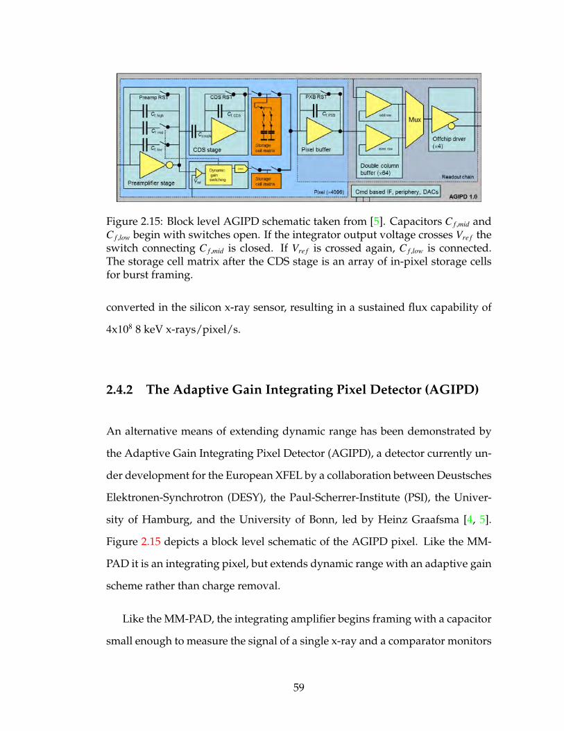
Figure 2.15: Block level AGIPD schematic taken from [5]. Capacitors C f ,mid andC f ,low begin with switches open. If the integrator output voltage crosses Vre f theswitch connecting C f ,mid is closed. If Vre f is crossed again, C f ,low is connected.The storage cell matrix after the CDS stage is an array of in-pixel storage cellsfor burst framing.
converted in the silicon x-ray sensor, resulting in a sustained flux capability of
4x10⁸ 8 keV x-rays/pixel/s.
2.4.2 The Adaptive Gain Integrating Pixel Detector (AGIPD)
An alternative means of extending dynamic range has been demonstrated by
the Adaptive Gain Integrating Pixel Detector (AGIPD), a detector currently un-
der development for the European XFEL by a collaboration between Deustsches
Elektronen-Synchrotron (DESY), the Paul-Scherrer-Institute (PSI), the Univer-
sity of Hamburg, and the University of Bonn, led by Heinz Graafsma [4, 5].
Figure 2.15 depicts a block level schematic of the AGIPD pixel. Like the MM-
PAD it is an integrating pixel, but extends dynamic range with an adaptive gain
scheme rather than charge removal.
Like the MM-PAD, the integrating amplifier begins framing with a capacitor
small enough to measure the signal of a single x-ray and a comparator monitors
59
the amplifier output. When the integrator is approaching saturation, the com-
parator signals the control logic, and a second capacitor, this one significantly
larger, is connected in parallel to the first (C f ,mid in figure 2.15). By increasing the
total feedback capacitance, the gain of the integrator is reduced and saturation is
avoided. As demonstrated in previous sections, sensitivity to single x-rays may
be lost with the additional feedback capacitance, but under these conditions the
integrated signal is already larger than a single x-ray, so the reduced resolution
is tolerable so long as shot noise remains the dominant source of uncertainty. A
third capacitor, larger still, is available in the event that saturation is reached a
second time.
When reading out, the AGPID transmits the integrated signal as an analog
value in addition to a second value which indicates the final gain stage engaged
while framing. In this way the AGIPD achieves a full well of more than 104
x-rays per pixel per frame. There are minimal instantaneous flux limitations on
the pixel. This is important because the pixel is designed for use at the Euro-
pean XFEL, where x-ray pulses with durations on the order of femtoseconds
will have to be measured. The AGIPD provides a means of integrating arbitrar-
ily short x-ray pulses with up to 104 12 keV x-rays/pixel/pulse. In contrast, the
MM-PAD can integrate arbitrarily short x-ray pulses of up to 200 8 keV x-rays
and experiences count rate limitations for larger pulses. The limitation is set
by the rate of charge removal. However, the maximum full-well and thus dy-
namic range of the AGIPD is still constrained by capacitor size, and thus pixel
size. The MM-PAD full well is set by the depth of a digital counter, which scales
exponentially with number of bits and is in general drastically smaller than ca-
pacitors in CMOS. With a significantly deeper full well, the MM-PAD can inte-
grate sustained fluxes of up to 4x10⁸ 8 keV x-rays/pixel/s. While the adaptive
60

Figure 2.16: Transfer characteristics of the AGIPD detector pixels. The three re-gions plotted represent the three gain settings of the AGIPD. The gain setting atreadout is dependent on incident signal. The dynamic range spans four ordersof magnitude at 12.4 keV. Plot adapted from [5].
gain scheme implemented in the AGIPD is powerful, increasing dynamic range
much further requires capacitor sizes that may be unreasonable.
Later in this dissertation a pixel architecture will be described which com-
bines the advantages of the AGIPD and the MM-PAD into a single high dynamic
range pixel. First however, we aim to demonstrate the importance of dynamic
range in x-ray detectors for synchrotron science with some concrete examples.
61

CHAPTER 3
APPLICATION OF DETECTORS
3.1 Introduction
This chapter discusses an experiment utilizing the MM-PAD, an x-ray detector
developed by the Gruner group. The purpose of this discussion is to illustrate
the importance of high dynamic range detectors in synchrotron science. The
work described here is a diffraction study of uranium dioxide under pulsed
magnetic fields conducted at the Advanced Photon Source (APS) experimental
hutch 6-ID-C. My collaborators included Zahir Islam from the APS, Jacob Ruff
from CHESS, Krzysztof Gofryk and Daniel Antonio from Idaho National Lab,
and Kate Shanks from the Gruner group at Cornell University.
Two benefits of high dynamic range detectors will be examined. Higher
dynamic range allows for finer temporal resolution and the measurement of
small signals which can provide important information that would otherwise
be drowned out by larger signals.
3.2 Uranium dioxide background
Nuclear fission of uranium dioxide provides upwards of 20% of the world’s
power. The thermal conductivity of uranium dioxide governs the conduction of
heat produced by fission which is ultimately converted to electricity, and thus
understanding this property is vital. While the material has been studied exten-
sively since the Manhattan Project, some elastic and magnetic properties remain
62
poorly understood. Uranium dioxide exhibits a first order transition to an anti-
ferromagnetic state at 30.8 K [55], and abrupt changes in unit cell volume have
been observed around this temperature [56]. The material has a cubic lattice
(CaF type 2) at room temperature. Unit cell changes at the Neel temperature are
theorized to be the result of Jahn-Teller distortions in the oxygen cage around
the uranium atoms [57]. Application of strong magnetic fields have been found
to amplify these distortions. The coupling of magnetic and elastic properties in
uranium dioxide could have profound implications on the present understand-
ing of this material’s thermophysical properties.
Bulk measurements have shown that above the Neel temperature magnetic
fields applied along the 〈111〉 lattice vector compress the unit cell along this
axis and expansion in transverse directions is observed. However, below the
Neel temperature the reverse is observed: magnetic fields applied in the 〈111〉
direction induce elongation of the unit cell, and constriction occurs perpendic-
ular to the applied field. Recent studies have found that reversing the direc-
tion of the applied magnetic field after cooling the uranium dioxide below the
Neel temperature can also reverse the contraction [58]. This behavior is indica-
tive of piezomagnetism which, in addition to magnetostriction, suggests that
a magnetic moment can be induced by physical strain on the material. Quan-
titatively, piezomagnetism implies a linear coupling between a material’s me-
chanical strain and magnetic polarization. Very few piezomagnetic materials
are known to exist.
In uranium dioxide, switching of the piezomagnetic behavior occurs at ±18
T. In practice, the sign of lattice expansion relative to magnetic field direction is
set by application of magnetic fields >18 T in one direction and is only reversed
63

when fields >18 T are applied in the opposite direction. If this behavior is the
result of piezomagnetism, with a coercive field strength of 18 T, uranium dioxide
is the strongest piezomagnet ever observed.
The inter-atomic interactions of uranium dioxide are ripe for exploration.
Bulk measurements yield net crystallographic properties, but single crystal
diffraction is arguably the best way to directly measure unit cell changes. For
example, while a net expansion transverse to the 〈111〉 axis has been measured
in bulk, whether this is due to a uniform shift in unit cells or twinning of crys-
tallographic grains can not be discerned. Below, an experiment to further in-
vestigate these phenomena is discussed. In this experiment, a detector with a
high dynamic range is essential to obtain high resolution data of phenomena
in pulsed magnetic fields and to discern the fine details of the sample’s atomic
distortion.
3.3 Experimental design
The experiments described below were conducted at experimental hutch 6-ID-
C at the Advanced Photon Source (APS). The APS is a third generation syn-
chrotron source with a 1104 m circumference storage ring described in [59].
Experimental hutch 6-ID-C is fed by an undulator through a double Si 〈111〉
monochromator with a 3.2-28 keV energy range. Energy resolution is ∆E/E ≈
10−4. A 3-stripe vertical focusing mirror with 60 cm active area is used to reject
higher harmonic photons and focus the beam to < 1 mm.
64

3.3.1 Pulsed magnet
The 6-ID-C hutch contains a novel apparatus for collecting diffraction data from
a sample mounted in a cryogenic solenoid which is connected to a 10 kV, 500 kJ
capacitor bank. Samples can be exposed to pulsed magnetic fields >30 T ev-
ery ∼12 minutes with a peak field time > 1 ms. The custom designed solenoid
enables x-ray scatter from samples to be collected over a roughly 23.6o arc in for-
ward scatter or back scatter geometries while under maximum magnetic field,
as described in [60]. Adjustment of sample position within the magnet allows
a larger arc of diffraction to be collected at lower peak fields, but this was not
explored in the work described here.
To control the peak magnetic field, and to control the duration of the mag-
netic field pulse, a choke coil is place in series between the capacitor bank and
the magnet. Capacitor charging voltage can also be used to limit peak magnetic
field on a per-pulse basis. The greatest limitation to high throughput data acqui-
sition is the cooling rate of the solenoid. Due to finite impedance of the magnet
coils, heat is generated with each pulse. To minimize physical damage to the
solenoid the pulse rate is limited.
Samples are cantilevered on a thermally conductive and electrically insulat-
ing arm, made of single crystal sapphire, into the bore of the magnet. The arm
thermally couples the sample to a closed cycle cryostat which can cool samples
to below 10 K. The sample chamber, including the magnet, is sealed. The mag-
net itself sits in a liquid nitrogen bath which is thermally independent from the
sample cryostat. Motors control the translation of the sample in three mutually
perpendicular directions and rotation on both axes perpendicular to the x-ray
beam. Magnetic fields are applied along the axis of the beam.
65

3.3.2 Uranium measurements
The sample is a 1mm x 1mm x 500µm (height x width x depth from the beam’s
perspective) single crystal block of uranium dioxide with the 〈111〉 face pol-
ished. The sample is mounted with the 〈111〉 surface facing the beam. The mag-
net is positioned so that the 〈888〉 diffraction condition is met in back-scatter.
Beam defining slits set the beam size on the sample to roughly 200µm x 200µm.
The beam flux is 3.5x10¹² 15.85 keV x-rays/s.
Figures 3.1 through 3.3 illustrate the geometry of the experiment1. Further
discussion of typical diffractometer geometries can be found in many sources.
For an overview of the methods used here, see the equatorial and moving-
crystal-moving-detector methods described in Chapter 2 of Single Crystal
Diffractometry by Arndt [61].
Zero field θ− 2θ maps were taken of the sample at 40 K and 14 K to measure
lattice constants and verify the expected sample contraction based on previous
bulk measurements, roughly ∼ 100 micro-strain. Strain refers to the change in a
dimension relative to the unstrained dimension. In this case, the lattice constant
has changed by 10−4 times its original value, 5.47 , due to a phase transition at
30.8 K. Figure 3.4 is the θ − 2θ map at 18 K. This map is produced by taking
images of the sample at a range of sample θ values (angle of the sample relative
to the beam). Each image is integrated in the polar angular direction χ (per-
pendicular to the plane of θ and 2θ, as shown in figure 3.3) to obtain the total
diffracted intensity at a given sample θ angle across the range of 2θ angles sub-
tended by the detector. Figure 3.5 is a single frame taken of the uranium dioxide
〈888〉 diffraction peak at 14 K.
1Figures 3.1 through 3.3 were drawn by Alexandra Westbrook
66
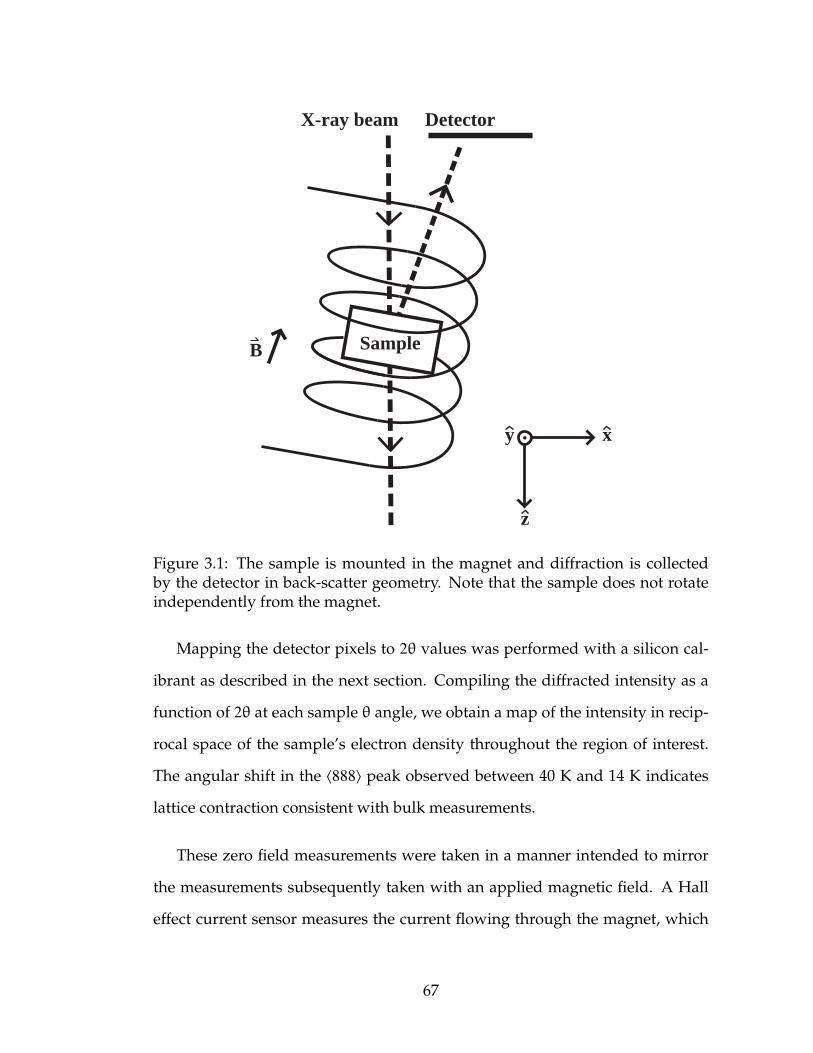
X-ray beam Detector
B
x
z
y
Sample
Figure 3.1: The sample is mounted in the magnet and diffraction is collectedby the detector in back-scatter geometry. Note that the sample does not rotateindependently from the magnet.
Mapping the detector pixels to 2θ values was performed with a silicon cal-
ibrant as described in the next section. Compiling the diffracted intensity as a
function of 2θ at each sample θ angle, we obtain a map of the intensity in recip-
rocal space of the sample’s electron density throughout the region of interest.
The angular shift in the 〈888〉 peak observed between 40 K and 14 K indicates
lattice contraction consistent with bulk measurements.
These zero field measurements were taken in a manner intended to mirror
the measurements subsequently taken with an applied magnetic field. A Hall
effect current sensor measures the current flowing through the magnet, which
67
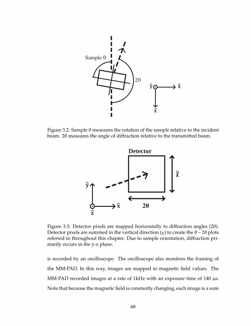
2θ
Sample θ
x
z
y
Figure 3.2: Sample θ measures the rotation of the sample relative to the incidentbeam. 2θ measures the angle of diffraction relative to the transmitted beam.
2θ
χ
Detector
xz
y
Figure 3.3: Detector pixels are mapped horizontally to diffraction angles (2θ).Detector pixels are summed in the vertical direction (χ) to create the θ− 2θ plotsreferred to throughout this chapter. Due to sample orientation, diffraction pri-marily occurs in the y-x plane.
is recorded by an oscilloscope. The oscilloscope also monitors the framing of
the MM-PAD. In this way, images are mapped to magnetic field values. The
MM-PAD recorded images at a rate of 1kHz with an exposure time of 140 µs.
Note that because the magnetic field is constantly changing, each image is a sum
68

Figure 3.4: Uranium dioxide θ−2θ plot measured at zero field and 14 K. The ver-tical lines in the intensity are artifacts resulting from gaps between the MM-PADdetector modules. This plot serves as a baseline for comparison of diffractionfrom the sample with magnetic fields applied.
of diffraction from all of the magnetic field values visited during the exposure.
In analysis, frames were assigned to the time-averaged magnetic field applied
throughout the exposure.
Figure 3.6 plots one magnet pulse versus time with MM-PAD exposures
highlighted. Because the gaps in time between frames is large relative to the
exposure time, measurements were repeated with an altered delay between the
triggering of the magnetic field pulse and the start of MM-PAD framing, sam-
pling more intermediate magnetic field values.
69

Figure 3.5: Sample frame of uranium dioxide diffraction peak 〈888〉 at roomtemperature. The color scale is logrithmic and the exposure time was 10 ms. Thepeak flux is close to the maximum measurable by the MM-PAD. Gaps betweenthe modules of the MM-PAD are also visible.
3.3.3 Azimuthal calibration
To interpret the measured data in this experiment, the detector’s position rel-
ative to the beam and sample needed to be measured. The calibration process
70
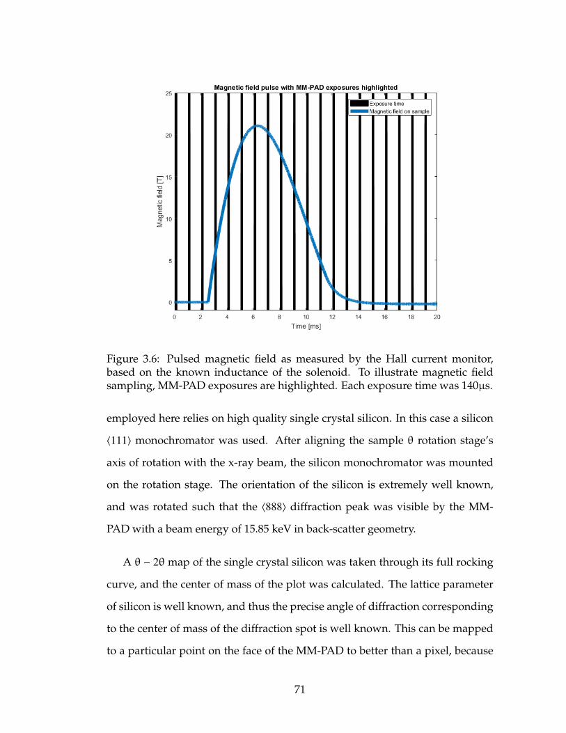
Figure 3.6: Pulsed magnetic field as measured by the Hall current monitor,based on the known inductance of the solenoid. To illustrate magnetic fieldsampling, MM-PAD exposures are highlighted. Each exposure time was 140µs.
employed here relies on high quality single crystal silicon. In this case a silicon
〈111〉 monochromator was used. After aligning the sample θ rotation stage’s
axis of rotation with the x-ray beam, the silicon monochromator was mounted
on the rotation stage. The orientation of the silicon is extremely well known,
and was rotated such that the 〈888〉 diffraction peak was visible by the MM-
PAD with a beam energy of 15.85 keV in back-scatter geometry.
A θ − 2θ map of the single crystal silicon was taken through its full rocking
curve, and the center of mass of the plot was calculated. The lattice parameter
of silicon is well known, and thus the precise angle of diffraction corresponding
to the center of mass of the diffraction spot is well known. This can be mapped
to a particular point on the face of the MM-PAD to better than a pixel, because
71

the diffraction spot spans several pixels in the back-scatter geometry.
The energy of the beam was then shifted to 15.99 keV, which also shifts the
angle which satisfies the Bragg condition. A second θ − 2θ map was taken,
and again the center of mass was mapped to a position on the MM-PAD. The
spacing between pixels is well known, as this is set by a lithographic process
with resolution much smaller than the pixel pitch of 150µm. With knowledge of
the diffraction angles and the points at which the diffraction struck the detector
we can obtain very accurate measurements of the distance from the beam to
the detector perpendicular to the beam and the distance from the detector to
the sample along the axis of the beam, as illustrated in figure 3.7 and calculated
below.
The sample to detector distance along the axis of the beam is ds. The distance
between the diffraction spot on the detector and the beam, perpendicular to
the beam, is d1 for the lower energy and d2 for the higher energy. θ1 and θ2
are the complements to the angles of diffraction at lower and higher energy
respectively. The distance on the surface of the detector between centers of Si
〈888〉 diffraction is dp. Note that d2 = d1 + dp.
We know that tan(θ1) = d1ds
and tan(θ2) = d2ds
. It follows that
tan(θ1)tan(θ2)
=d1
d2=
d1
d1 + dp(3.1)
which allows us to solve for d1. Given that the difference dp was the difference
in pixels in only the horizontal direction, this allows us to solve for all of the
desired quantities. Furthermore, this provides knowledge of the azimuthal an-
gular coordinate of each pixel on the face of the MM-PAD given the position
at which the detector is mounted. Note that by ignoring vertical displacement,
we are assuming that the vertical angle of the diffraction is small relative to the
72
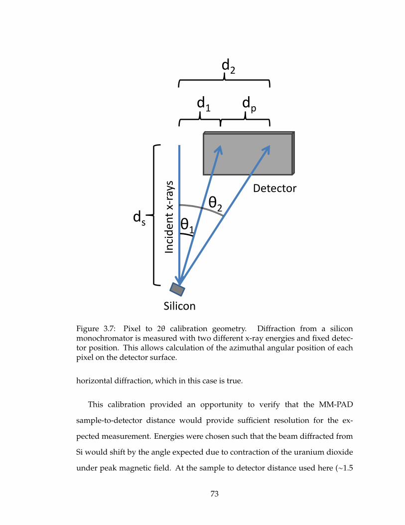
θ1
θ2ds
d1 dp
d2
Detector
Silicon
Inci
de
nt
x-ra
ys
Figure 3.7: Pixel to 2θ calibration geometry. Diffraction from a siliconmonochromator is measured with two different x-ray energies and fixed detec-tor position. This allows calculation of the azimuthal angular position of eachpixel on the detector surface.
horizontal diffraction, which in this case is true.
This calibration provided an opportunity to verify that the MM-PAD
sample-to-detector distance would provide sufficient resolution for the ex-
pected measurement. Energies were chosen such that the beam diffracted from
Si would shift by the angle expected due to contraction of the uranium dioxide
under peak magnetic field. At the sample to detector distance used here (∼1.5
73

m) the diffraction center of mass sweeps across forty pixels on the MM-PAD.
3.4 Data analysis
The magnet was pulsed at a set of sample θ positions. Each frame was assigned
a magnetic field value according to the oscilloscope measurements discussed
above. Sorting frames by magnetic field and sample orientation yields the set
of θ − 2θ plots in figure 3.8. These plots provide a view of what the uranium
dioxide unit cell is doing throughout the magnetic field pulse. Note that more
than ten magnetic field values were sampled per pulse, and not all measured
magnetic field values are plotted below.
The slight intensity variation in the diagonal direction, along the strips of
integrated intensity, are artifacts resulting from much finer sampling in 2θ than
sample θ. One sample θ value (position of sample rotation stage) can be sam-
pled per pulse while more than two hundred 2θ values (pixels across the detec-
tor) are sampled per pulse. As a result, the axes in figure 3.8 have very different
scales and the intensity in reciprocal space appears to jump in 2θ with each step
of sample θ.
To more readily interpret this behavior, the θ−2θ plots were collapsed to the
sample θ = θ line. Bins were drawn with boundaries perpendicular to a line
with slope 1/2 in the θ − 2θ plots and the sum of integrated intensity in each
bin forms one point in the plot in figure 3.9. Each row of this plot shows the
intensity in reciprocal space of the uranium dioxide sample along the reciprocal
lattice vector 〈hhh〉. The plot’s vertical axis is magnetic field.
74
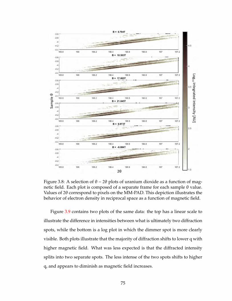
Figure 3.8: A selection of θ − 2θ plots of uranium dioxide as a function of mag-netic field. Each plot is composed of a separate frame for each sample θ value.Values of 2θ correspond to pixels on the MM-PAD. This depiction illustrates thebehavior of electron density in reciprocal space as a function of magnetic field.
Figure 3.9 contains two plots of the same data: the top has a linear scale to
illustrate the difference in intensities between what is ultimately two diffraction
spots, while the bottom is a log plot in which the dimmer spot is more clearly
visible. Both plots illustrate that the majority of diffraction shifts to lower q with
higher magnetic field. What was less expected is that the diffracted intensity
splits into two separate spots. The less intense of the two spots shifts to higher
q, and appears to diminish as magnetic field increases.
75
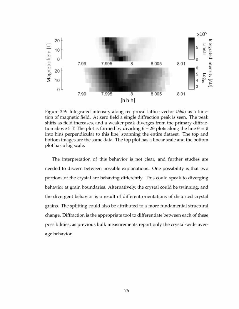
Figure 3.9: Integrated intensity along reciprocal lattice vector 〈hhh〉 as a func-tion of magnetic field. At zero field a single diffraction peak is seen. The peakshifts as field increases, and a weaker peak diverges from the primary diffrac-tion above 5 T. The plot is formed by dividing θ − 2θ plots along the line θ = θ
into bins perpendicular to this line, spanning the entire dataset. The top andbottom images are the same data. The top plot has a linear scale and the bottomplot has a log scale.
The interpretation of this behavior is not clear, and further studies are
needed to discern between possible explanations. One possibility is that two
portions of the crystal are behaving differently. This could speak to diverging
behavior at grain boundaries. Alternatively, the crystal could be twinning, and
the divergent behavior is a result of different orientations of distorted crystal
grains. The splitting could also be attributed to a more fundamental structural
change. Diffraction is the appropriate tool to differentiate between each of these
possibilities, as previous bulk measurements report only the crystal-wide aver-
age behavior.
76

3.4.1 Future work
The experiment described above is ongoing. Recently, high current, high volt-
age switches have been added to pulsed magnet at the APS experimental hutch
6-ID-C to enable rapid switching of the pulsed magnet polarity. This enables
the training of uranium dioxide below 30.8 K with a magnetic field pulse > 18
T in one direction, and subsequently retraining the sample in the opposite di-
rection to investigate potential piezomagnetic effects. Further analysis of the
current data, as well as additional data taking to increase the range of 2θ values
measured under pulsed fields is being performed.
These techniques are also being applied to new, similar samples. Namely,
pulsed magnet work is now being performed on uranium nitride (UN) and ura-
nium antimonide (USb). Each of these samples have shown potential for inter-
esting magneto-elastic behavior of their own. The techniques described above
will be expanded on and improved.
3.5 Necessity of high dynamic range
In the experiment described above, greater magnetic field resolution is obtain-
able through magnetic pulse extension, so that the rate of magnetic field change
is lower, or through shorter exposure times. Pulse elongation is possible with a
larger choke coil, but this would decrease the maximum magnetic field applied
to the sample. Shorter exposure times are also possible, but the measured sig-
nal is the exposure time multiplied by flux. The signal to noise ratio must be
maintained at a high enough value to resolve the diffraction of interest. Here
77

the importance of high dynamic range, particularly the ability to measure large
instantaneous flux, is clear. In the case of the MM-PAD, the main beam re-
quired minor attenuation due to the flux limitation of the detector, as discussed
in Chapter 2.
With a higher dynamic range, finer sampling of magnetic field values would
be possible resulting in less blurring due to the transient nature of the mag-
netic field in this experiment. This is related to the case of XFEL experiments on
dynamic systems. XFEL pulses with sub-picosecond durations allow dynamic
processes to be imaged with commensurate temporal resolution. However, this
is only possible if the detector in use can record a sufficient number of x-rays
in this time window. In addition to fine magnetic field sampling, high dynamic
range is required to perform this experiment in a reasonable time frame. Given
that data in this experiment is acquired for 12 miliseconds per 12 minutes, a
detector which required more beam attenuation may require multiple pulses to
measure a significant signal from each sample orientation. Beam-time at syn-
chrotron sources is a limited resource, and a high dynamic range detector helps
to maximize its utilization.
Figure 3.5 depicts a single frame from a zero field scan of the uranium sam-
ple. Details in the texture of this Bragg peak can reveal more detailed informa-
tion about the sample, and is an intriguing direction for future studies. For
example, whether separate peaks move together or separately could hint at
whether the splitting of diffracted intensity is due to twinning or some other
behavior. In any case, these data are only accessible with a high dynamic range
detector. Even in the 140 µs exposure times used in this experiment, peak sig-
nals of nearly 105 x-rays/pixel are measured. Alongside these, the signal from
78

the secondary diffraction peak are more than three orders of magnitude smaller.
While the AGIPD detector could resolve this difference in intensity, it might
saturate with the exposure times used here. However, it could utilize shorter
exposure times effectively.
On the other hand, a Photon counting detector would experience extreme
pileup under these signal rates of > 5x10⁸ x-rays/pixel/s. To utilize a pho-
ton counting detector here, the beam must be attenuated by several orders of
magnitude. Note that the dimmer peak in figure 3.9 is more than an order of
magnitude weaker than the primary peak. This plot is the sum of many frames,
however, and the dimmer peak was often more than three orders of magnitude
weaker than the dominant peak in the raw data, depending on sample orienta-
tion and magnetic field strength. If the attenuation required to prevent pileup
effects in photon counting detectors were used, the dim peak might not be dis-
cernible from background scatter at all.
79
CHAPTER 4
THE HIGH DYNAMIC RANGE DETECTOR CONCEPT
Chapter 3 illustrated the importance of dynamic range to expanding exper-
imental possibilities and fully utilizing synchrotron capabilities. The MM-PAD
demonstrates that charge removal circuitry is a valuable tool to extend mea-
surable signal levels when a large, sustained x-ray signal is to be measured.
Pushing this metric further would permit better utilization of high brightness
storage ring sources. X-ray free electron lasers present a different set of chal-
lenges to x-ray detector development.
The AGIPD’s adaptive gain, discussed in Chapter 2, is designed to integrate
signals from XFELs, which produce high intensity x-ray pulses with durations
on the order of femtoseconds. It would seem that charge removal is ill-suited to
the problem of integrating large XFEL pulses because no circuitry can respond
on femtosecond time scales.
However, the peak photocurrent generated in pixels by XFEL pulses is not
quite as dire as femtosecond x-ray pulse durations suggest. While an entire
XFEL pulse reaches a detector in the span of femtoseconds, drift, diffusion, and
the plasma effect cause the resulting photocurrent to take significantly longer to
arrive at pixel integration nodes [62]. Some work has been done in the devel-
opment of the AGIPD to mitigate this effect. The AGIPD seeks to integrate all
of the charge from a single pulse as quickly as possible to achieve higher frame
rates [63]. However, it may be possible to utilize the delayed arrival of pho-
tocurrent due to the plasma effect in such a way that charge removal circuitry
can extend x-ray detector dynamic range at XFEL sources as well as storage ring
sources.
80

This chapter discusses our efforts to characterize the plasma effect and eval-
uate the possibility of developing an x-ray detector which uses charge removal
to integrate very short duration, high intensity x-ray pulses. The detector frame-
work devised and discussed herein is also intended to further extend measur-
able sustained x-ray flux such that the detector would prove useful at all fourth
generation x-ray sources.
4.1 Measuring the plasma effect
The plasma effect refers to the case when a sufficiently large number of electron-
hole pairs are generated in a sufficiently small volume of a photo-sensor so as to
behave like a plasma cloud. High intensity x-ray pulses can lead to the plasma
effect in silicon diodes. An electron-hole plasma expels the photodiode electric
field which would ordinarily separate charge carriers and bring them to respec-
tive sensor terminals. Instead of the charge cloud being separated in bulk, the
surface of the plasma cloud is wicked away by the expelled electric field while
the interior of the plasma remains relatively shielded. This slows down the ac-
cumulation of photocurrent at pixel integration nodes.
To better understand this process, and to assess the prospect of charge re-
moval operation at XFELs, we have utilized the transient current technique to
measure photocurrent transients from a pixelated silicon diode illuminated by
a focused infrared laser.
Infrared laser wavelengths were chosen to match the attenuation length of
x-ray photons in silicon. For example, 950 nm infrared light has the same atten-
uation length in silicon at room temperature as 8 keV x-rays. As a result, absorp-
81

tion of an intense 950 nm laser pulse in a silicon diode produces an electron-hole
pair distribution in the sensor which is similar what would be expected from a
pulse of 8 keV x-rays. Table 4.1 enumerates several x-ray energies along with
their attenuation length in silicon and the IR wavelength with the same attenu-
ation length in silicon. Figure 4.1 is a graphical comparison.
X-ray Energy Attenuation IR WavelengthLength in Silicon
2 keV 1.53 µm 547 nm4 keV 9.68 µm 780 nm6 keV 30.3 µm 893 nm8 keV 67.8 µm 950 nm
10 keV 130 µm 992 nm12 keV 224 µm 1016 nm14 keV 353 µm 1033 nm16 keV 521 µm 1046 nm18 keV 734 µm 1055 nm
Table 4.1: Table listing some x-ray energies, their attenuation length in silicon,and the IR wavelength with a matching attenuation length in room temperaturesilicon. X-ray attenuation lengths were drawn from the NIST database [64], andIR photon attenuation lengths were drawn from [65].
X-ray energy [keV] IR photon wavelength [nm]
Att
en
uat
ion
len
gth
in s
ilico
n [μ
m]
12keV 1016nm
Figure 4.1: Attenuation length in silicon of x-rays (left) matches attenuationlength in silicon of IR photons (right). The green line highlights the correspon-dence of 12 keV photons to 1016 nm photons. In this way, IR laser pulses cansimulate XFEL pulses.
We built on previous studies [66], increasing the laser intensity employed by
two orders of magnitude, to investigate the delay of photocurrent collection due
82
to the so-called plasma effect. We hope to maximally exploit this mechanism,
extending charge collection times of femtosecond XFEL pulses to microseconds.
This extended pulse duration may allow for charge removal techniques, per-
haps modifications of the technique employed in the MM-PAD, to be used at
XFELs.
4.1.1 Experimental apparatus
1 Data was collected by focusing a tunable, pulsed IR laser (EKSPLA PT259-AO-
H) to a 5 ± 1µm rms spot on a custom diode modeled after the variety intended
for use with the HDR-PAD which is described in the next subsection. Figure 4.3
depicts the experimental apparatus and beam path. The laser pulse duration
was 10.5ps FWHM as measured by the manufacturer. The laser was equipped
with a pulse picker which enables a user defined pulse repetition rate below the
laser’s natural 1MHz rate. The tunable wavelength range was 700 nm − 1050
nm with a line width between 0.18 nm − 0.36 nm. The precise line width varies
throughout the wavelength range of the laser.
As mentioned above, the purpose of a selectable wavelength is to simulate x-
rays of different energies. Computational simulations were performed to ensure
that the finite line width (FWHM of the power spectral density) of the laser
would be sufficiently small, assuming a Gaussian distribution of wavelengths
in the pulse. Figure 4.2 plots the generated hole density of a simulated laser
pulse in one micron slices of a silicon sensor versus sensor depth for a 1016 nm
laser pulse. A larger line width, particularly at longer wavelengths where the
1Dr. Julian Becker provided invaluable assistance in developing this apparatus and perform-ing these measurements.
83

attenuation length in silicon of IR photons changes more rapidly as a function of
wavelength, leads to electron-hole pairs being created at different depths in the
sensor than intended. Based on these simulations it was determined that a sub-
nanometer line width had a negligible effect on the distribution of electron-hole
pairs in the sensor.
0 50 100 150 200 250
Depth into sensor [7m]
10-30
10-20
10-10
100
1010
1020
1030
Hol
e de
nsity
[hol
es/m
3]
1016nm high energy IR pulse hole density in Si versus depth
Linewidth = 0.1nmLinewidth = 0.5nmLinewidth = 1.0nmLinewidth = 2.0nmLinewidth = 5.0nm
Figure 4.2: Simulated hole density created in one micron slices of a silicon sensoras a function of depth into the sensor for a laser pulse of 1016 nm wavelengthphotons with various spectral distributions at normal incidence. The laser pulsewas simulated with 6 µm pulse radius and 1011 eV pulse energy at room tem-perature.
The maximum pulse energy was > 107 keV. Pulse-to-pulse energy variations
were measured with a 1% silvered mirror which directed a fraction of pulse en-
ergy to an ancillary diode, hereafter referred to as the beam-split diode. The
84

beam-split diode read out its measured transient alongside the main pulse sig-
nal transient to a DPO 7254C oscilloscope with a 2.5GHz bandwidth. The beam-
split diode was calibrated with J-10GE-LE Quantum EnergyMax pyroelectric
laser pulse energy meter. The pyroelectric pulse energy meter produces a volt-
age pulse in response to a change in sensor temperature due to incident laser
pulses. The energy meter selected is NIST calibrated and serves to pair beam-
split diode measurements with absolute pulse energies. During calibration, the
pyroelectric energy meter was placed at the sample diode location. By taking
a series of measurements with both the beam-split diode and the energy meter,
the correspondence between beam-split measurements and actual pulse energy
arriving at the sample was measured.
The beam path consists of the aforementioned 1% silvered mirror followed
by a filter wheel. The filter wheel allowed larger variations in pulse energy to be
explored, but no filter was used when measuring peak pulse energy photocur-
rent transients. The filter wheel is followed by a Galilean telescope to expand
the pulse to the subsequent achromatic doublet lens’s full aperture to maxi-
mize beam focusing. The target diode and support electronics were mounted
on translation stages which were controlled by the same computer which con-
trolled the laser, permitting parametric scans.
Target photodiode
A custom diode array was designed to read photocurrent transients directly to
an oscilloscope while mirroring the sensors used in previous x-ray detectors
built by our group as closely as possible. The diode array is 500µm thick n-type
high resistivity silicon with a 120V depletion voltage and 150µm x 150µm pixel
85

Laser Beam Sampler Custom Diode
Oscilloscope Aperture and Lens Telescope Filter Wheel
Figure 4.3: Laser beam path for transient current technique studies. The pulsedinfrared laser is controlled by a computer (not shown) which coordinates theoscilloscope readings. Laser pulses pass through a beam sampler which con-sists of an 1% silvered mirror at 45 degrees to the beam path. A dedicated diodereads the fractional pulse to record pulse-to-pulse energy variations. The mainpulse then passes through a filter wheel which enables large scale pulse inten-sity variation. The pulse is subsequently expanded through a Galilean telescopeto permit tighter focus by the achromatic doublet lens. The focused pulse is ab-sorbed by a custom silicon photo diode and the photocurrent transient is routedto the oscilloscope through a custom PCB. The main pulse transient and splitpulse transient are read by the oscilloscope to the data acquisition computer.
pitch. The pixelated structure of the diode enabled measurement of the lateral
diffusion of the charge cloud.
The diodes employed in Gruner group x-ray detectors are biased by ap-
plication of a high voltage via an aluminum layer on the x-ray entrance side.
This layer is essentially transparent to x-rays, but would be significantly more
opaque to infrared photons. As such, an opening in the aluminum above tar-
get pixels was required. The diode included four target pixels below the alu-
minum opening in a 2x2 square. These target pixels were surrounded by sev-
eral rings of non-target pixels. In a pixelated sensor, the uniformity of voltage
across adjacent pixels is essential. If adjacent pixels are held at different biases,
charge deposited above one pixel may enter another, resulting in image distor-
tion. In this customized diode, it was necessary to maintain voltage control of
86

non-target pixels. Non-target pixels were ganged together by uniform back-side
aluminization which could be biased by a single wire bond. Because no ASIC
layer was being designed to accompany the sensor, photocurrent of interest was
to be routed through wire bonds to support electronics. Each of the four target
pixels was individually wire bonded.
Wire bonds were made to a custom printed circuit board (PCB). The PCB to
which the sensor was wire bonded also provided the high voltage bias. The PCB
was designed by Dr. Julian Becker with a metal lined hole to which the entrance
window of the target diode was attached with silver paint. The high voltage bias
was supplied through the hole’s metalization and laser pulses struck the target
pixels through the hole in the PCB. Circuitry on the PCB capacitively coupled
target pixels to an amplifier which fed measured transients to an oscilloscope.
Schematics for the PCBs employed in this work are contained in Appendix A.
While measuring the incident photocurrent, slight variation in the target
pixels’ voltages were unavoidable, but a bias-tee, consisting of a connection
to the bias voltage through an inductor, and a connection to the readout am-
plifier through a capacitor, ensured that the pixel would quickly return to an
AC ground. Similar bias-tees were used to bias non-target pixels and the sen-
sor. These signals were also measured. Photocurrent transients were terminated
with 50Ω and measured by a Tektronix DPO 7254C oscilloscope. All lines were
terminated with 50Ω to minimize the impact of reflections on signal lines.
87

4.1.2 Transient current analysis
A single IR photon in the wavelength range studied here does not have suffi-
cient energy to create an electron-hole pair in silicon. As a result, absorption
of IR photons in silicon is phonon assisted, and in subsequent analysis, it is
assumed that each IR photon creates one electron-hole pair. Studies of high
intensity sub-band gap radiation incident on silicon have noted a power depen-
dance in the absorption of photons in silicon and the onset of significant nonlin-
ear effects such as two-photon absorption [67]. Optical nonlinearities are often
characterized by the Kerr coefficient, in silicon for IR photons is on the order
of 10−18 m2/W [68]. The present experiment utilizes a peak laser power on the
order of 40 watts with a spot size of roughly 36 µm2. This suggests that changes
in the index of refraction of silicon during absorption of the laser pulses used
here are on the order of 10−6 and so these nonlinear effects should be negligible.
In comparing IR pulse energy to x-ray pulse energies, it is thus necessary to
calculate the number of IR photons in a given pulse. This is done by first as-
suming that the pulse is monochromatic. Given the small line width of the laser
employed, this is a reasonable assumption. The absolute energy of the laser
pulses used here were calibrated as described in the section above. With the ab-
solute energy known and monochromaticity assumed, the number of photons
in a given pulse is simply the pulse energy divided by the energy of a single
photon, hcλ
. We then assume that this is the number of electron-hole pairs cre-
ated in the silicon diode by this pulse. By matching the attenuation length of
the IR pulse wavelength to that of an x-ray energy, we divide the x-ray energy
by 3.6eV (the energy required to create an electron-hole pair in silicon), and di-
vide the number of electron hole pairs created by the IR pulse by this number
88
to arrive at the equivalent x-ray pulse energy.
Because the plasma effect is a function of illuminated volume, laser spot size
needed to be measured. The opening in the target diode high voltage biasing
aluminization which allowed IR pulses to strike target pixels, described in the
previous section, provided a convenient knife edge with which to measure the
laser pulse profile. By translating the target diode perpendicular to the incident
beam while collecting pulse data from target pixels, such that the aluminization
blocks part of the incident pulses, we can plot a curve which is the signal mea-
sured by the target pixels as a function of pulse position. The derivative of this
curve tells us the laser intensity that is cut off from the target pixels by the high
voltage aluminization with each translation step. This provides a reconstruction
of the lateral pulse profile. Figure 4.4 is a plot of one of these scans with a one
micron step size and a Gaussian fit to the data. The fitted standard deviation is
< 6µm. To obtain information longitudinal to the beam, which includes infor-
mation about pulse focusing, this procedure was performed at various lens-to-
diode distances.
Photocurrent transients from XFEL-like pulses have the characteristic shape
illustrated in Figure 4.5, which is an average of one hundred 950 nm photocur-
rent transients from laser pulses which create electron-hole pair distributions
similar to 106 8 keV photons, measured with 200V sensor bias. Generally speak-
ing, photocurrent arrives in two phases: an initial spike arising largely from
induced current [69] followed by a long tail as charge carriers drift to the sensor
terminals. In the transient plotted, roughly 10% of total deposited charge arrives
in the spike followed by a tail photocurrent roughly equivalent to that produced
by 1011 8keV x-rays/s. However, these numbers vary significantly based on fac-
89

2.029 2.03 2.031 2.032 2.033 2.034 2.035 2.036 2.037 2.038
Y-Stage Position [7m] #104
-0.2
0
0.2
0.4
0.6
0.8
1
1.2
Nor
mal
ized
HV
Pho
tocu
rren
t [A
U]
Derivative of 950nm pulse scan across sensor opening edge Gaussian fit to data: < = 5.256
datafit
Figure 4.4: Gaussian fit to derivative of lateral translation scan of target diodewith 950nm laser incident. The fitted line describes the laser pulse profile in onedimension perpendicular to the beam path.
Figure 4.5: Characteristic shape of photocurrent transients produced by highintensity pulses (> 104 x-rays). The transient above is an average of one hundred950 nm pulses (equivalent to 8 keV attenuation length) with a mean single pulseenergy equivalent to 106 8 keV x-rays. The sensor was bias was 200 V.
90
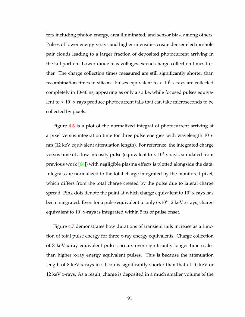
tors including photon energy, area illuminated, and sensor bias, among others.
Pulses of lower energy x-rays and higher intensities create denser electron-hole
pair clouds leading to a larger fraction of deposited photocurrent arriving in
the tail portion. Lower diode bias voltages extend charge collection times fur-
ther. The charge collection times measured are still significantly shorter than
recombination times in silicon. Pulses equivalent to < 103 x-rays are collected
completely in 10-40 ns, appearing as only a spike, while focused pulses equiva-
lent to > 104 x-rays produce photocurrent tails that can take microseconds to be
collected by pixels.
Figure 4.6 is a plot of the normalized integral of photocurrent arriving at
a pixel versus integration time for three pulse energies with wavelength 1016
nm (12 keV equivalent attenuation length). For reference, the integrated charge
versus time of a low intensity pulse (equivalent to < 103 x-rays, simulated from
previous work [66]) with negligible plasma effects is plotted alongside the data.
Integrals are normalized to the total charge integrated by the monitored pixel,
which differs from the total charge created by the pulse due to lateral charge
spread. Pink dots denote the point at which charge equivalent to 104 x-rays has
been integrated. Even for a pulse equivalent to only 6x10⁴ 12 keV x-rays, charge
equivalent to 104 x-rays is integrated within 5 ns of pulse onset.
Figure 4.7 demonstrates how durations of transient tails increase as a func-
tion of total pulse energy for three x-ray energy equivalents. Charge collection
of 8 keV x-ray equivalent pulses occurs over significantly longer time scales
than higher x-ray energy equivalent pulses. This is because the attenuation
length of 8 keV x-rays in silicon is significantly shorter than that of 10 keV or
12 keV x-rays. As a result, charge is deposited in a much smaller volume of the
91

Figure 4.6: Normalized integrated charge versus integration time of 1016 nm(12 keV equivalent attenuation length) pulses at three pulse energies. The reddotted line is a low energy pulse (< 103 x-rays, simulated from previous work[66]) for reference. Sensor bias was 200 V.
Figure 4.7: Average pulse duration as a function of total pulse energy at threewavelengths. Pulse durations were measured as time above two times the stan-dard deviation of background noise. Sensor bias was 200 V.
92
sensor, leading to denser electron-hole pair clouds and therefore more persis-
tent plasma effects. Charge collection times of 12 keV equivalent IR pulses do
not reach more than 1 µs with the spot size and pulse energies tested here, but
the charge collection times measured are still significantly longer than the laser
pulse duration.
Figure 4.8: Averaged photocurrent traces from 950nm laser pulses focused to 6µm incident on a 500 µm thick silicon diode. The diode bias was 200 V.
Figure 4.8 shows plots of averaged photocurrent transients from a range of
950 nm pulse energies versus time. The plasma effect is evident in the depen-
dance of charge collection time on pulse energy.
93
4.1.3 Conclusions
Figure 4.5 is an average of one hundred 950 nm pulse photocurrent transients
with a mean pulse energy that produced electron-hole pairs equivalent to 106 8
keV x-rays. This profile is characteristic of all measured pulses which exhibited
signs of the plasma effect. Overall, the charge collection profile is extremely sen-
sitive to wavelength, spot size, and pulse energy. However, some conclusions
can be drawn.
The plasma effect is most pronounced for lower energy x-ray equivalents
which produce denser plasma clouds. Thus, the strategy of using plasma clouds
to slow charge arrival is more promising for 8 keV x-ray pulses, compared to the
other x-ray equivalents tested here. Charge collection times for sufficiently fo-
cused pulses do extend to microsecond time scales. Despite the extended charge
collection time, significant photocurrent still arrives in the initial spike and may
prove problematic for pulse energies greater than 106 8 keV x-rays.
A strategy to integrate pulses of this nature may be possible and might in-
volve adaptive gain handling integration of the initial photocurrent spike and
charge removal circuitry handling the drawn out tail. While in-pixel charge
removal techniques are not fast enough to act on femtosecond time scales, we
have shown that photocurrent from large pulses can arrive over microseconds,
a time scale on which MM-PAD style charge removal techniques may prove
useful.
94
4.2 Adaptive gain and charge removal combined
The ”spikes“ measured in the IR laser pulse photocurrent transients above de-
posit too much charge in pixels too quickly for a charge removal scheme to ac-
curately record signals. An adaptive gain scheme is capable of measuring these
signal bursts, but the full well of an adaptive gain pixel is ultimately limited by
integration capacitor size, and therefore, pixel size. The full well scales linearly
with these quantities. The charge removal of the MM-PAD achieves a full well
that is limited by the depth of a digital counter, which doubles with each suc-
cessive bit added. The tradeoff is of course that photocurrent integration now
has a rate limitation.
Combining an adaptive gain scheme with a charge removal scheme similar
to that of the MM-PAD provides two primary benefits. First, the ”spike“ of
intense x-ray pulses can be integrated by the adaptive gain circuitry. As seen
above, the majority of signal charge arrives over a longer time scale, perhaps
long enough for charge removal circuitry to operate. If this tail arrives after
adaptive gain circuitry has already activated, it is possible to use a larger charge
removal capacitance. The maximum flux measurable by one MM-PAD pixel in
its present form is
Φ = ∆V ∗Crem ∗ f /qx (4.1)
where Φ is the maximum flux, ∆V is the voltage difference between the front
end voltage and Vlow, Crem is the size of the charge removal capacitance, f is
the maximum frequency of charge removal, and qx is the number of electron-
hole pairs created per x-ray. Crem should not exceed Cint, the integration ca-
pacitance, or charge removal could result in pulling the integrator out of its
operating range and produce erroneous measurements. Adaptive gain allows
95

Crem to be increased by several orders of magnitude by virtue of Cint increasing
step-wise, thus increasing the maximum flux measurable by a pixel employing
charge removal.
In addition to possibly integrating XFEL like pulses studied in this chapter,
combining adaptive gain with charge removal allows pixels to integrate a signif-
icantly higher sustained x-ray flux. This capability would be exceedingly useful
at high brightness storage ring sources. Chapter 5 will outline several pixel ar-
chitectures which utilize both adaptive gain and charge removal circuitry. An
ASIC with pixel test structures pursuant to this strategy was fabricated, and
their testing is discussed.
96

CHAPTER 5
PIXEL SUBSTRUCTURE TESTING
Combining charge removal with adaptive gain could increase the dynamic
range attainable by a pixel array detector at XFELs and high brightness syn-
chrotron sources by several orders of magnitude. To roughly estimate the po-
tential gains, consider the performance of the MM-PAD, described in Chapter 2.
The MM-PAD is capable of measuring a sustained flux of 108 8 keV x-rays per
pixel per second. With an adaptive gain front-end increasing the integration
capacitance by, say, a factor of 25, the charge removal capacitance can be corre-
spondingly increased, resulting in a factor of 25 higher sustained flux limit. It
may also be possible to increase the maximum rate of charge removal, which
would further extend this limit. A factor of 4 increase in the rate of charge re-
moval would result in a net sustained flux 100 times higher than the MM-PAD.
As seen in the previous chapter, such a pixel could potentially measure high
intensity XFEL pulses as well.
Extending the performance of a pixel array detector pixel is not trivial. For
example, increasing the maximum rate of charge removal too much will result
in incomplete elimination of integrated charge, and thus produce an unreliable
measurement. Furthermore, the MM-PAD relies on holding the front-end at a
fixed voltage to ensure the uniformity of charge removal operations. To achieve
this, the front-end amplifier will have to respond quickly to large signals with a
correspondingly high slew rate.
To examine the feasibility of a detector utilizing both adaptive gain and
charge removal in the same pixel, an ASIC was fabricated with several pro-
totype pixel front-end architectures in TSMC 180nm mixed signal general-
97

purpose II 1P6M salicide technology with 2 fF/µm2 MIM-caps and thick top
metal through Europractice.1 This chapter discusses these prototype pixel de-
signs and their ability to integrate high currents. Chapters 6 and 7 discuss a
16x16 pixel, fully functional pixel array detector constructed with pixel archi-
tectures based on the designs discussed below.
The work discussed here was a collective effort. While all team members
worked together, the majority of developmental work on particular components
can generally be attributed to particular scientists. The MM-PAD 2.0 pixel was
developed by Dr. Katherine Shanks, the charge dump oscillator was developed
by Dr. Hugh Philipp, and I developed the capacitor flipping pixel. FPGA pro-
gramming to orchestrate the chip’s operation was written by Prafull Purohit and
the support electronics were designed and laid out by Darol Chamberlain. Dr.
Mark Tate and Professor Sol Gruner were also instrumental in the development
of these structures.
5.1 Pixel architectures
This section discusses the concepts and architectures of three pixels that were
designed. The test ASIC discussed in this chapter generally featured only the
pixel front-ends, excluding components such as digital counters and analog
readout chains. In two cases, adaptive gain was not included, but the inte-
gration capacitance was chosen to simulate the low gain stage of an adaptive
gain system. A full adaptive gain system was omitted in these pixels to test
1At the time of the writing of this dissertation, all relevant design files are located onthe Gruner group server “People” in directory /us/Detectors-EssentialInformation/HDR-PAD/HDR-PAD_Sub1/.
98
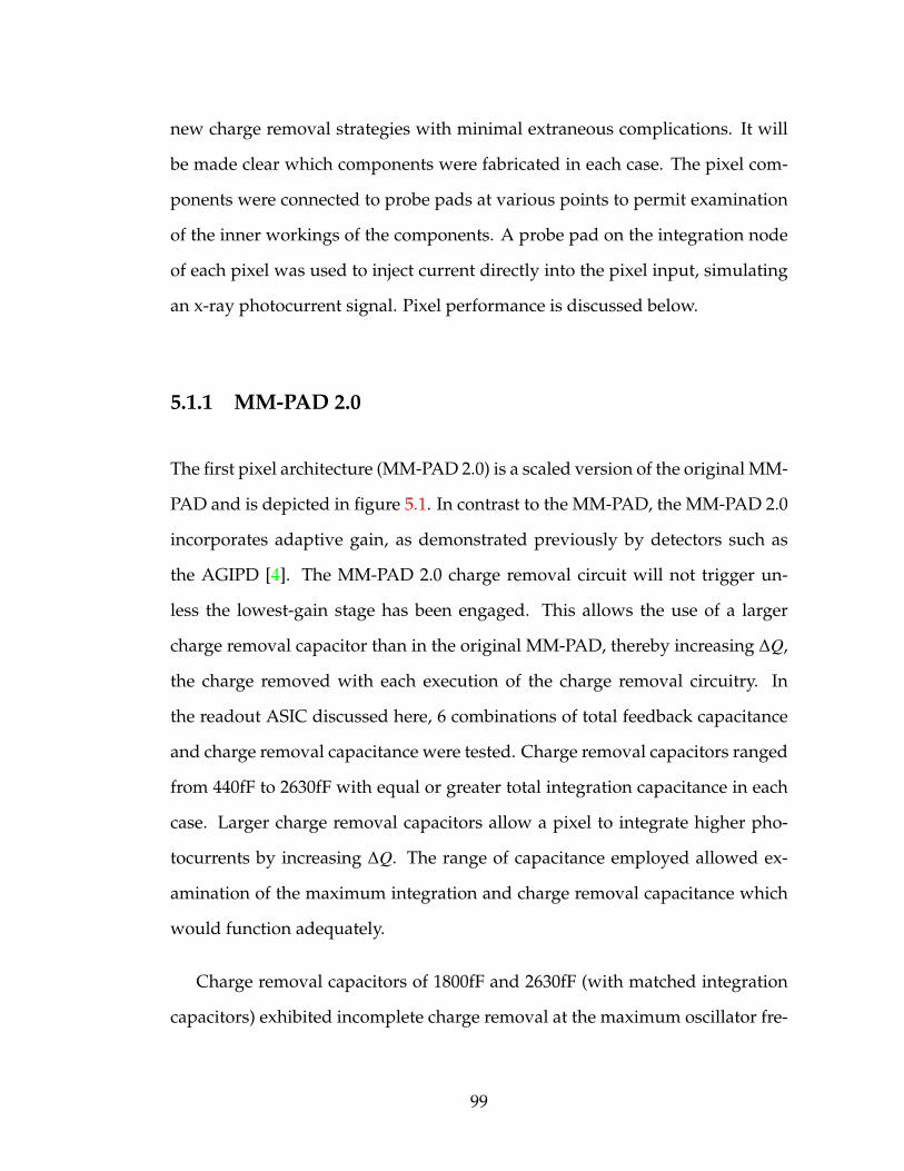
new charge removal strategies with minimal extraneous complications. It will
be made clear which components were fabricated in each case. The pixel com-
ponents were connected to probe pads at various points to permit examination
of the inner workings of the components. A probe pad on the integration node
of each pixel was used to inject current directly into the pixel input, simulating
an x-ray photocurrent signal. Pixel performance is discussed below.
5.1.1 MM-PAD 2.0
The first pixel architecture (MM-PAD 2.0) is a scaled version of the original MM-
PAD and is depicted in figure 5.1. In contrast to the MM-PAD, the MM-PAD 2.0
incorporates adaptive gain, as demonstrated previously by detectors such as
the AGIPD [4]. The MM-PAD 2.0 charge removal circuit will not trigger un-
less the lowest-gain stage has been engaged. This allows the use of a larger
charge removal capacitor than in the original MM-PAD, thereby increasing ∆Q,
the charge removed with each execution of the charge removal circuitry. In
the readout ASIC discussed here, 6 combinations of total feedback capacitance
and charge removal capacitance were tested. Charge removal capacitors ranged
from 440fF to 2630fF with equal or greater total integration capacitance in each
case. Larger charge removal capacitors allow a pixel to integrate higher pho-
tocurrents by increasing ∆Q. The range of capacitance employed allowed ex-
amination of the maximum integration and charge removal capacitance which
would function adequately.
Charge removal capacitors of 1800fF and 2630fF (with matched integration
capacitors) exhibited incomplete charge removal at the maximum oscillator fre-
99
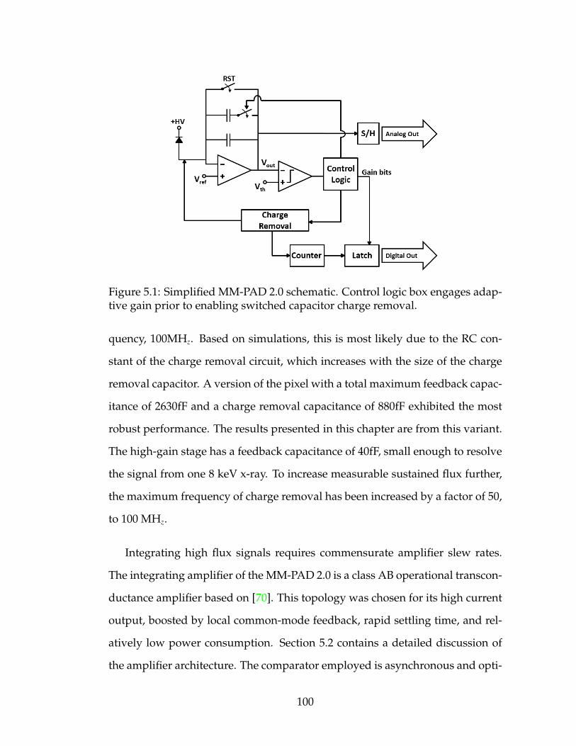
Figure 5.1: Simplified MM-PAD 2.0 schematic. Control logic box engages adap-tive gain prior to enabling switched capacitor charge removal.
quency, 100MHz. Based on simulations, this is most likely due to the RC con-
stant of the charge removal circuit, which increases with the size of the charge
removal capacitor. A version of the pixel with a total maximum feedback capac-
itance of 2630fF and a charge removal capacitance of 880fF exhibited the most
robust performance. The results presented in this chapter are from this variant.
The high-gain stage has a feedback capacitance of 40fF, small enough to resolve
the signal from one 8 keV x-ray. To increase measurable sustained flux further,
the maximum frequency of charge removal has been increased by a factor of 50,
to 100 MHz.
Integrating high flux signals requires commensurate amplifier slew rates.
The integrating amplifier of the MM-PAD 2.0 is a class AB operational transcon-
ductance amplifier based on [70]. This topology was chosen for its high current
output, boosted by local common-mode feedback, rapid settling time, and rel-
atively low power consumption. Section 5.2 contains a detailed discussion of
the amplifier architecture. The comparator employed is asynchronous and opti-
100

Figure 5.2: MM-PAD 2.0 gated oscillator and charge removal switched capacitorblock level schematics.
mized for response time. It is composed of a five transistor differential amplifier
driving an inverter. These components varied only slightly between the three
pixel architectures discussed in this chapter.
The pixel components fabricated in this test ASIC include the front-end inte-
grating amplifier with full adaptive gain and charge removal circuitry. Charge
removal control signals, adaptive gain control signals, and comparator output
were connected to probe pads for external measurement alongside the integra-
tor analog output and front-end voltages.
MM-PAD 2.0 charge removal
The charge removal circuitry, depicted in figure 5.2, consists of a gated oscillator
which toggles a switched capacitor to remove charge from the integration node
(pixel front-end). The gated oscillator pulse width and maximum frequency is
set by Cosc1,2 and the tunable current mirror Mosc. Cosc1 and Cosc2 are equal sized
101

capacitors. It is the same topology as the original MM-PAD. When the com-
parator activates the NAND gate, the Cosc capacitors begin charging. Once its
voltage passes the inverter threshold, the inverters connect Crem to the pixel in-
tegration node and Cosc begins discharging. Once the capacitors Cosc1,2 have dis-
charged, the charge removal signal is brought low again. The charge removed
per oscillator pulse is
∆Q = Crem(Vre f − Vlow). (5.1)
The MM-PAD 2.0 can tolerate larger photocurrent spikes (integrating > 103 x-
rays before relying on charge removal) and larger sustained photocurrents than
the original MM-PAD.
5.1.2 Charge dump oscillator
The charge dump oscillator (CDO) pixel design aims to scale the rate of charge
removal with the rate of charge arrival by combining the charge removal
switched capacitor with the oscillator driving it. Depicted in figure 5.3, the fre-
quency of charge removal is set by the propagation of digital signals in the ring
oscillator and the charging rate of the removal capacitor, Crem. When a compara-
tor indicates that a threshold has been crossed, the oscillator is activated and
Crem connects to the integration node. Once Crem has charged to the switching
threshold of the adjacent inverter, the capacitor is detached and the charge ac-
cumulated onto it is dumped to ground. The faster Crem charges while attached
to the front-end, the faster charge is removed.
In addition to one comparator monitoring the integrator output, as in the
MM-PAD, a second comparator monitors the pixel front-end voltage. Charge
102
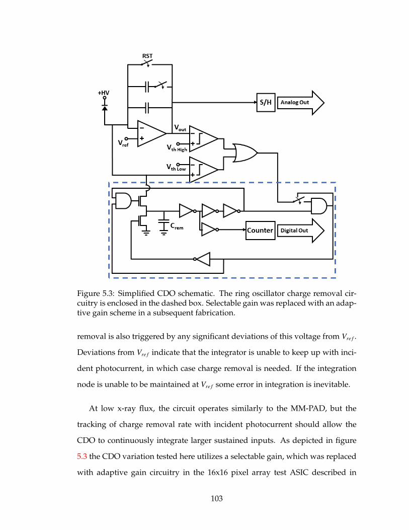
Figure 5.3: Simplified CDO schematic. The ring oscillator charge removal cir-cuitry is enclosed in the dashed box. Selectable gain was replaced with an adap-tive gain scheme in a subsequent fabrication.
removal is also triggered by any significant deviations of this voltage from Vre f .
Deviations from Vre f indicate that the integrator is unable to keep up with inci-
dent photocurrent, in which case charge removal is needed. If the integration
node is unable to be maintained at Vre f some error in integration is inevitable.
At low x-ray flux, the circuit operates similarly to the MM-PAD, but the
tracking of charge removal rate with incident photocurrent should allow the
CDO to continuously integrate larger sustained inputs. As depicted in figure
5.3 the CDO variation tested here utilizes a selectable gain, which was replaced
with adaptive gain circuitry in the 16x16 pixel array test ASIC described in
103

Chapter 6. Additionally, the integrating amplifier studied here is a simple, five
transistor differential amplifier. The amplifier is intentionally incapable of high
current integration. Its use was intended to ensure that the pixel in this test ASIC
would rely more heavily on the charge dump oscillator circuitry. The amplifier
has been replaced by a class AB amplifier similar to that of the MM-PAD 2.0
in subsequent pixel iterations. Both comparators in the pixel are asynchronous,
composed of a five transistor differential amplifier driving two inverters.
The pixel components fabricated in this test ASIC include the integrating
amplifier with selectable gain and the full charge dump oscillator circuitry with
comparators monitoring both the front-end voltage and integrating amplifier
analog output voltage. Both comparator output signals, the in-pixel OR combi-
nation of them, the oscillator output, and the integrating amplifier output volt-
age were buffered off chip for external measurement.
Charge dump oscillator charge removal
The CDO charge removal circuitry is depicted in the dashed box in figure 5.3.
The timing of charge removal is controlled by the charging of Crem, but rather
than a current source controlling the rate of charging as in the MM-PAD 2.0,
the rate of charging is controlled by the rate at which charge is pulled from
the integration node. The charge removal timing capacitor is also the charge
removal capacitor. In this way, the charge removal rate can increase when the
front-end integration node is flooded with signal charge. The amount of time
that Cosc is connected to the front-end also depends on the switching threshold
of the first inverter in the chain. While the inverter thresholding of the CDO
is very fast, it is more susceptible to fabrication process variation than the other
104

designs presented here. In this case, variation could result in different quantities
of charge removed per cycle in each pixel. Although this can be calibrated, it is
an additional complication. The charge removed per charge removal execution
is
∆Q = CoscVre f . (5.2)
as Crem discharges to ground.
5.1.3 Capacitor flipping pixel
The third pixel front-end fabricated and tested relies on a charge removal
method based on the flipped capacitor filter described in [71]. The capacitor
flipping pixel integrator uses two equally sized integration capacitors connected
in parallel, depicted in figure 5.4. One of the two integration capacitors is con-
nected via a network of CMOS switches so as to allow the capacitor’s polarity
in the circuit to be reversed. Adaptive gain was not incorporated in the initial
fabrication and is not shown in figure 5.4, but it was implemented in the 16x16
pixel array test ASIC described in Chapter 6.
Referring to figure 5.4, the pixel begins integration with the switches labeled
”A“ closed and the switches labeled ”B“ open. Charge is integrated onto both
equal-sized capacitors in parallel. When the integrator output crosses the com-
parator threshold, the comparator fires. This activates the control logic which
opens switches ”A“. After a brief delay to prevent shorting the integration ca-
pacitors, switches ”B“ are closed. This reverses the orientation of half of the
integration capacitance. As a result, integrated positive charge on each capac-
itor neutralizes negative charge on the other capacitor. Thus, the integrator is
105

Figure 5.4: Simplified capacitor flipping pixel schematic. Dynamic thresholdingcircuitry is enclosed in the dotted box. An adaptive gain scheme was imple-mented in the most recent fabrication.
effectively reset, and can continue integrating photocurrent. Subsequent flip-
ping occurs as needed. Connections to the flipping capacitor are always broken
before new connections are made.
As with each other charge removal circuit, ∆Q depends on the front-end volt-
age of the integrator. To reduce the error introduced by changes in the front-end
voltage due to large current spikes, a dynamic thresholding circuit was devised.
Control was added such that dynamic thresholding can be toggled externally:
the pixel comparator can use an external reference voltage to define the thresh-
old at which capacitor flipping is initiated, or it can be set dynamically. In the
dynamic case, a level-shifted copy of the front-end voltage is used to set the ca-
pacitor flipping threshold voltage. This ensures that there is a specific voltage
across the integration capacitance at the time of the comparator firing, precisely
the level shift voltage. However, due to the dependance of ∆Q in this method
106

on both the integrator input and output nodes, an input rate dependent error
is introduced by delays in the capacitor flipping control logic. These errors are
investigated in section 5.3.2.
The dynamic thresholding block level schematic is depicted in figure 5.4.
The level shift is set by a diode drop within the pixel, though this was changed
in subsequent interation of the pixel. The integrating amplifier of the capacitor
flipping pixel is a class AB amplifier similar to that of the MM-PAD 2.0, but op-
timized independently. The comparator is again asynchronous: a five transistor
differential amplifier driving two inverters. The gated oscillator which controls
the capacitor flipping is a ring oscillator.
This pixel components fabricated in this test ASIC include the integrating
amplifier, capacitor flipping switches and control logic, make-before-break cir-
cuitry, and an externally toggled dynamic thresholding circuit. Capacitor flip-
ping signals A and B, comparator output, front-end voltage, integrating ampli-
fier analog output voltage, and the level-shifted threshold voltage were buffered
off chip for measurement.
Capacitor flipping pixel charge removal
Make before break circuitry ensures that the integration capacitor to be flipped
is disconnected before it is reconnected in reversed orientation. This prevents
shorting the integration capacitors, which would neutralize signal charge in an
uncontrolled way. Maximum rate of charge removal and charge removal pulse
width is set by an inverter chain delay. The duration of this delay was set based
on simulation to ensure complete charge neutralization between capacitor flips.
107

The charge removed per charge removal execution depends on the integrator
output voltage:
∆Q = 2Cint(Vre f − Vout). (5.3)
The factor of two accounts for charge on both capacitors being neutralized as Cint
is half of the total integration capacitance. Vout is the output voltage sampled at
the time of Cint disconnect. Dynamic thresholding aims to keep Vre f − Vout at a
fixed value in each charge removal execution.
5.2 Integrating amplifier
Each of the three pixel architectures tested here utilize similar integrating ampli-
fiers. The integrating amplifier of the CDO in this test ASIC is not the topology
discussed below, but subsequent iterations of the pixel do use this architecture.
The design goals of the pixels discussed here are demanding. In general, to
measure a large photocurrent with a charge sensitive amplifier, an equal cur-
rent must be supplied by the amplifier. A flux of 1011 8 keV x-rays absorbed in a
silicon photodiode corresponds to more than 35µA photocurrent. The integrat-
ing amplifier of these pixels must be capable of outputs on this level. However,
these pixels should be designed with scaling in mind. Ideally, the pixels would
be fabricated in an array of 128x128 pixels, more than sixteen thousand total
pixels, so the in-pixel circuitry must have a low average power consumption.
Additionally, an amplifier used with a charge removal system must be ca-
pable of high slew rates in both positive and negative directions. The amplifier
must have an output that keeps up with incident photocurrent, but also brings
the front-end voltage back to its quiescent point quickly after each charge re-
108

moval execution. For these reasons a class AB topology based on the work of
Carvajal et al. was chosen [70].
Class AB amplifiers combine the benefits of both class A and class B am-
plifiers while attempting to minimize their shortcomings. Class A amplifiers
maintain a constantly biased output stage and thus exhibit minimal output dis-
tortions for signals in their full range. However, poor power efficiency and
current utilization are inevitable in conditions where the full bias current is
not required by the load being driven. A class A amplifier in the pixels dis-
cussed above would consume far too much power because the maximum drive
required is very large. On the other hand, class B amplifier outputs are nearly
off in quiescent conditions. The cost of this low power consumption is signal
distortion in some input regimes.
Here a two stage AB topology is used in an effort to optimize both gain
and output swing, as the full well of an integrator is linearly proportional to its
output swing. The disadvantages of a multi-stage amplifier include added com-
plexity, increased power consumption, and reduced bandwidth. These tradeoff
can be mitigated and in this case are ultimately worthwhile.
Slight variations of the topology depicted in figure 5.5 were implemented
in each of the pixels discussed in this dissertation. The amplifiers were indi-
vidually tuned in each pixel, but the general operating principals are the same.
To understand the architecture, we can break the schematic into several parts.
Transistors M1 and M2 are the input transistors. The output stage is composed
on transistors M4 and M8. Transistors symmetric about a vertical line down the
middle of the schematic are matched in size.
109
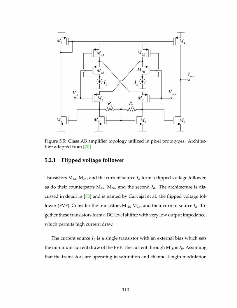
Figure 5.5: Class AB amplifier topology utilized in pixel prototypes. Architec-ture adapted from [70].
5.2.1 Flipped voltage follower
Transistors M1A, M2A, and the current source IB form a flipped voltage follower,
as do their counterparts M1B, M2B, and the second IB. The architecture is dis-
cussed in detail in [72] and is named by Carvajal et al. the flipped voltage fol-
lower (FVF). Consider the transistors M1B, M2B, and their current source IB. To-
gether these transistors form a DC level shifter with very low output impedance,
which permits high current draw.
The current source IB is a single transistor with an external bias which sets
the minimum current draw of the FVF. The current through M1B is IB. Assuming
that the transistors are operating in saturation and channel length modulation
110

is negligible,
IB = I1B =12µpCox
W1B
L1B(Vs1 − Vin+ − Vthp)2, (5.4)
where µp is the hole mobility, Cox is the gate-oxide capacitance per unit area, WmLm
is the width to length ratio of transistor m, Vsm is the source voltage of transistor
m, and Vthp is the PMOS threshold voltage. For the sake of concision in this
chapter, the term µn,pCoxWmLm
will be defined
βm ≡ µn,pCoxWm
Lm(5.5)
for transistor m, where the applicable mobility can be inferred from the schemat-
ics referenced.
Given equation 5.4, we know that
Vs1 =
√2IB
β1B+ Vin+ + Vthp, (5.6)
which is a level shifted copy of Vin+. Similarly,
Vs2 =
√2IB
β1A+ Vin− + Vthp. (5.7)
The input of one half of the amplifier linearly shifts the source voltage of the in-
put transistor in the other half. This adaptive biasing applies differential inputs
to both the gate and source of the input transistors, doubling the transconduc-
tance of the differential pair. As a result, the amplifier can be biased such that
the quiescent current is low, but a differential signal will still initiate a strong
response.
The current through the input transistor M1 is then
I1 =β1
2
√
2IB
β1B+ V∆
2
(5.8)
111

where V∆ ≡ Vin+ − Vin−. The current through the input transistors flows to the
current sinks M6 and M7 and sets the output voltages which serves as the input
voltages for the second stage of the amplifier. Before examining the output stage
however, we must address resistors R1 and R2 which set the bias on the current
current sinks and provide common mode feedback.
5.2.2 Local common mode feedback
The bias of M6 and M7 could be set externally, making them simple current mir-
rors. In this case, the maximum downward slew rate of the first stage would be
limited by this bias current. Matched resistors R1 and R2 are added to provide
local common mode feedback (LCMFB) as demonstrated in [70] and discussed
in [73]. For Vin+ = Vin− the current across these resistors is zero. If the voltage of
the first stage output nodes, Vd1 and Vd2, rise in unison, the gate voltage of the
current sources rises as well, and they sink more current to combat the change.
Similarly, decreases in the gate voltage are resisted. Transistors M6 and M7 be-
have like diode connected transistors for common mode signals. As such, they
have low output impedance
Rout ≈ 1/gm6 (5.9)
where gm6 is the transconductance of transistor M6. The gain of the first stage in
common mode conditions is therefore low. With V∆ = 0, I1,2 = I6,7 = IB and the
gate voltage of M6,7 is equal to the drain voltage of M1,2,
Vd1,2 = Vthn +
√2IB
β6,7, (5.10)
assuming saturation of M6,7 and matching of transistors M1,2 with M1B,1A.
112

However, when a differential signal is applied R1 and R2 maintain the gate
voltages of M6 and M7 at a common voltage, so the transistors behave more like
current sources. The first stage exhibits a higher output impedance:
Rout ≈ R1||ro1||ro6, (5.11)
where rom is the drain-source impedance of transistor m and Rn||Rm indicates the
resistance of Rn and Rm in parallel.
More quantitatively (following the work in [70]), for a differential signal
V∆ = Vin+ − Vin− a current flows through the feedback resistors R1,2. If channel
length modulation is negligible, M6 and M7 sink equal currents because they
have equal Vgs, so the current through the resistors is half the difference be-
tween branches, IR = (I1 − I2)/2. The current through M6 and M7 is the common
mode current, Icm = (I1 + I2)/2. The common gate voltage of M6 and M7 is
Vg6,7 = Vthn +
√2Icm
β6,7(5.12)
and the drain voltages of M1 and M2 respectively are
Vd1 = Vg6 + R1IR (5.13)
and
Vd2 = Vg7 − R2IR (5.14)
assuming Vin+ > Vin− and therefore I1 > I2. For Vin+ < Vin− the signs of the second
term in equations 5.13 and 5.14 are reversed.
Relative to externally biased current sources, the maximum downward slew
rate can be increased by the LCMFB, yet the first stage of the amplifier can be
designed with a low quiescent current ≈ 2IB. The adaptive action of the FVFs
113

and LCMFB aid in accomplishing the goal of low quiescent power consump-
tion with high gain. High slew rate in the first stage is important for a rapid
amplifier response. R1 and R2 can be implemented with externally biased MOS
transistors.
5.2.3 Amplifier output
Assuming that the output transistors operate in saturation and channel length
modulation is negligible, using equations 5.13 and 5.12, the current through
transistor M5 is
I5 =β5
2(Vd1 − Vthn)2 =
β5
2
√
2Icm
β6+ R1IR
2
. (5.15)
This current is mirrored to M4. If we assume that the differential signal is large
and positive, IR ≈ I1/2 and ICM ≈ I1/2. Under these conditions M8 is effectively
off and the output current is
Iout ≈ I5 =β5
2
√
I1
β6+
R1I1
2
2
. (5.16)
Referring to equation 5.8 for the value of I1 we see that
Iout ≈β5
2
R1β1
4V2
∆ +
√
β1
2β6+
R1β1
2
√IBβ1
β1B
V∆ +
√
IBβ1
β1Bβ6+
R1β1IB
2β1B
2
. (5.17)
If IB is small, this reduces to
Iout ≈β5
2
R1β1
4V2
∆ +
√β1
2β6V∆
2
. (5.18)
IB in the pixels discussed here is between 5-15µA. To leading order the output
current is proportional to V4∆. Conversely if V∆ is large and negative, the output
114

current is the current through M8,
Iout ≈β8
2
R2β2
4V2
∆ −
√
β2
2β6+
R2β2
2
√IBβ1
β1A
V∆ +
√
IBβ2
β1Aβ6+
R1β2IB
2β1A
2
. (5.19)
Again, if IB is small, we have
Iout ≈β8
2
R2β2
4V2
∆ −
√β2
2β6V∆
2
, (5.20)
where now we make the assumptions that IR ≈ I2/2 and ICM ≈ I2/2. Note that
V∆ is negative in equation 5.20 and the current here is flowing into the amplifier
through M8.
When V∆ is small, the current through the resistors is
IR =I1 − I2
2= V∆β1
√2IB
β1B(5.21)
from equation 5.8 and its M2 counterpart, noting that M1 and M2 are matched
transistors, as are M1A and M1B, so their β values are equal if we ignore process
variation. The common mode current is then
ICM =I1 + I2
2=β1IB
β1A+β1V2
∆
2, (5.22)
and the output current is
Iout = I4 − I8 = β5R1IR
√8ICM
β6. (5.23)
The small signal differential voltage gain of the first stage is
Vd1 − Vd2
Vin+ − Vin−= 2gm1(ro1||ro6||R1,2), (5.24)
noting that transistors on either side of the schematic in figure 5.5 are matched
and R1 = R2. The small signal gain of both stages combined is
Vout+ − Vout−
Vin+ − Vin−= 2gm1gm8(ro4||ro8)(ro1||ro6||R1,2). (5.25)
115
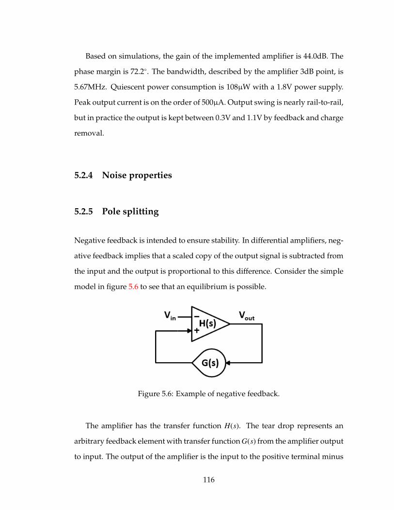
Based on simulations, the gain of the implemented amplifier is 44.0dB. The
phase margin is 72.2. The bandwidth, described by the amplifier 3dB point, is
5.67MHz. Quiescent power consumption is 108µW with a 1.8V power supply.
Peak output current is on the order of 500µA. Output swing is nearly rail-to-rail,
but in practice the output is kept between 0.3V and 1.1V by feedback and charge
removal.
5.2.4 Noise properties
5.2.5 Pole splitting
Negative feedback is intended to ensure stability. In differential amplifiers, neg-
ative feedback implies that a scaled copy of the output signal is subtracted from
the input and the output is proportional to this difference. Consider the simple
model in figure 5.6 to see that an equilibrium is possible.
Figure 5.6: Example of negative feedback.
The amplifier has the transfer function H(s). The tear drop represents an
arbitrary feedback element with transfer function G(s) from the amplifier output
to input. The output of the amplifier is the input to the positive terminal minus
116

the input to the negative terminal multiplied by the transfer function:
Vout = H(s)[Vin −G(s)Vout] (5.26)
Therefore the gain of the amplifier with feedback is
Vout
Vin=
H(s)1 + G(s)H(s)
. (5.27)
For large H(s), equation 5.27 is approximately equal to 1G(s) . The transfer
function of a high gain amplifier with negative feedback can be set by selection
of the feedback elements. This is because negative feedback functions similarly
to a restoring force in a stable physical system. If the output of the amplifier is
greater than the level dictated by the feedback elements, the subtraction of the
output at the amplifier’s input will bring the output back down. Similarly, if the
output is too small, a larger signal results from the subtraction operation. An
equilibrium is eventually reached as long as the feedback is subtracted from the
input. What would happen if the feedback was instead added? We would find
thatVout
Vin=
H(s)1 −G(s)H(s)
. (5.28)
In this case, if G(s)H(s) = 1 the gain of the system is infinity. Note that both G and
H are functions of s, a frequency dependent term. This is because in practice, the
transfer function of circuit elements is frequency dependent. Circuit elements
not only alter the voltage level of signals, but also induce a phase shift. If this
phase shift reaches 180, the negative feedback becomes positive feedback, and
the system is no longer stable.
Op-amps generally induce a phase lag with an absolute value that increases
from zero with increasing frequency. To ensure stability, the gain of a system
must be less than one for frequencies at which the phase shift is greater than
117

180. If it is not, the system will amplify the signal and oscillate at this frequency
indefinitely. An amplifier’s phase margin is defined as 180 minus the absolute
value of the phase shift imparted to signals at the unity gain frequency in open-
loop. The unity gain frequency is the frequency at which the amplifier’s open-
loop gain has dropped to one. The phase margin is a metric used to gauge
whether an amplifier will be stable in practice. Generally the value should be
kept greater than 45.
To ensure stability in some iterations of the amplifier in figure 5.5, pole split-
ting was employed. For a more detailed discussion of poles see [30]. The domi-
nant pole in the first stage of the class AB amplifier discussed here is the output
pole with frequency f = 1/[2π(R1||ro1||ro6)Cgs5]. Note that the gates of transistors
M6 and M7 are at virtual ground, so they do not contribute to this pole. The
dominant pole of the amplifier’s second stage is formed by the load capacitance
and the output impedance, Rout = ro4||ro8. By connecting a capacitor between the
amplifier output and the gate of M8, we accomplish Miller compensation [30].
The Miller effect enhances the impact of this capacitance, and the dominat poles
are shifted. The input pole is brought closer to the origin, while the output pole
is pushed to higher frequencies. The poles are ”split.“
The effect of pole splitting is to bring the unity gain frequency to a lower fre-
quency while pushing the frequency at which feedback signals are phase shifted
by 180 to higher frequencies. This reduces the overall amplifier bandwidth but
increases the phase margin to ensure stability.
118

5.3 Current injection tests
The three pixel front-ends were fabricated with several means of injecting a test
charge to emulate an input x-ray signal. A PMOS current source in each pixel
provided simple functionality tests. For higher currents and quantitative re-
sults, a copy of each pixel with a probe pad attached to its input was included
in fabrication. Current was injected into pixels through a tungsten needle with
a 10kΩ resistor between the needle and an external current source. The current
was generated and regulated by a Keithley 2400 Sourcemeter. Output signals
were buffered off chip to a DPO7254C Tektronix oscilloscope.
Parasitic capacitance of the needle probe was estimated to be ∼10pF. This es-
timate is based on the change of Vout in the MM-PAD 2.0 pixel during a charge
removal event. The integrating amplifier output voltage jumps during charge
removal to maintain Vre f on the front-end. The jump is smaller with the nee-
dle contacting the front-end because the needle’s parasitic capacitance reduces
the charge transfer efficiency of the integrating amplifier, i.e. charge removal
pulls some charge from the parasitic capacitance rather than the integration ca-
pacitance. This parasitic capacitance is significantly larger than the contribution
expected from a bump bonded sensor, which is closer to 200fF. Based on calcula-
tions of charge transfer efficiency and simulation results, this increased parasitic
capacitance reduces the maximum signals which can be properly integrated as a
result of reducing ∆Q. The capacitance also has a damping effect on pixel front-
end transient signals. Consequently this method is not suitable for testing pixel
performance under pulsed input, but these results do indicate the magnitude of
average input signal rates which can be integrated by the pixels under investi-
gation.
119
5.3.1 Probe pad current injection
To evaluate the linearity of integration for each pixel architecture, pixel output
was monitored with a constant current input. The measured output, charge re-
moval frequency, was multiplied by nominal ∆Q values (the quantity of charge
removed per removal execution) to calculate an inferred input current. This in-
ferred input current can then be compared to the actual, known input current.
These values are plotted against each other in figure 5.7. To measure the charge
removal frequency, buffered charge removal control signals were measured on
an oscilloscope, and edge finding algorithms were used to determine the time of
each charge removal cycle. Linear fits to the time of each charge removal versus
the number of charge removals preceding it yielded the charge removal period
as the slope of the fit. From this, frequency and uncertainty in the determina-
tion of the frequency were extracted. Variations in frequency between traces at a
given input current were larger than the uncertainty in the determination of the
frequency in a single trace, but both measures of uncertainty are smaller than
the data points plotted in figure 5.7. Voltages used in the calculation of charge
removal quantities were taken at their nominal values, e.g., V f ront−end was taken
as Vre f , which is set externally. Throughout this section, current is specified in
units of equivalent 8 keV x-rays/s. This is the flux of 8 keV x-rays that, when
absorbed in a reverse biased silicon photo diode, would produce an equivalent
photocurrent.
120

Iin
[Equivalent 8keV x-rays/s] #10110 1 2 3 4 5 6 7
I infe
rred
[Equ
ival
ent 8
keV
x-r
ays/
s]
#1011
0
1
2
3
4
5
6
7
CDOCap Flip External ThreshCap Flip Dynamic ThreshMM-PAD 2.0
0 0.1 0.2 0.30
0.1
0.2
0.3x1011
x1011
Figure 5.7: Inferred input currents based on pixel outputs versus actual inputcurrent. The dotted line represents an ideal response (inferred input equals ac-tual input). The charge dump oscillator is plotted with circles, the MM-PAD2.0 with triangles, the externally thesholded capacitor flipping pixel with dia-monds, and the dynamically thesholded capacitor flipping pixel with squares.Input and inferred current values are converted to the number of 8 keV x-raysabsorbed in silicon per second which would produce an equivalent photocur-rent. Inset: Magnification of the same data.
121

5.3.2 Performance and analysis
The MM-PAD 2.0 results are shown as triangles in figure 5.7. Good performance
is seen with inputs up to 1.3x10¹¹ 8 keV x-rays/s equivalent. The inferred cur-
rent measurement abruptly plateaus, indicating that the pixel oscillator is oper-
ating at its maximum frequency. These values are consistent with simulation.
Deviation from linearity is likely a result of process variation in charge removal
capacitor size and V f ront−end not being held precisely at Vre f . This can be cali-
brated.
The CDO results are shown as circles in figure 5.7. At low input currents,
the inferred input is greater than the actual input, which implies that ∆Q is less
than what is expected based on the value of Vre f . This could be a result of pro-
cess variation in capacitor size. Alternatively, incomplete charge removal may
occur because signals in the ring oscillator propagate quickly compared to time
constants associated with the charge dump process. If the dump is repeatable,
the digital gain of each pixel can be calibrated. However, because the switching
of the CDO is regulated by the threshold of an inverter, the stability of any cali-
bration is threatened over time by radiation damage which can result in device
threshold shifts.
As the input current increases, the CDO’s inferred input current drops be-
low the actual input current. In this regime, above 1011 x-rays/s, the quantity
of charge removed per charge removal execution exceeds the expected value.
A likely cause of this error is a significant rise in the pixel front-end voltage
above Vre f . This would cause more integrated charge to be removed from the
integration node than intended.
122

Iin
[Equivalent 8keV x-rays/s] #10110 1 2 3 4 5 6
Com
para
tor
Del
ay [n
s]
2
4
6
8
10
12
14
16SimulationMeasurement
Figure 5.8: Measured comparator delays from the capacitor flipping pixel withdynamic thresholding are plotted. Measured values assume that all deviationsfrom linearity in the capacitor flipping pixel’s output are a result of charge inte-grated during switching delays. Values from simulation are plotted as a dottedline.
Capacitor flipping pixel data was taken with both dynamic thresholding and
a fixed, external threshold. These data are plotted in figure 5.7 as squares and di-
amonds, respectively. Some error in externally thresholded operation is a result
of the integrator front-end voltage drifting upwards with higher input currents.
This drift was observed directly in testing. The decrease of inferred current
above 5×10¹¹ 8 keV x-rays/s equivalent input in the externally thresholded case
is likely a result of the front-end voltage being pushed outside of the integrating
amplifier’s range of optimal operating conditions.
A clear improvement in performance is seen with the dynamic thresholding
enabled. However, there is still substantial error in the input reconstruction:
123

less than 70% of the input is accounted for above 3.5 × 10¹¹ x-rays/s equivalent
input. This error can be explained by noting that the quantity of charge neutral-
ized per capacitor flip, ∆Q, depends on the voltage across the integrator, not just
the front-end voltage as in the other pixel designs. This means that any delay
between when the capacitor should be disconnected and when it actually does
disconnect can introduce error. Specifically, if photocurrent continues to be in-
tegrated during this delay, the output voltage of the integrator will continue to
drop and the charge neutralized will be greater than anticipated.
From these data we can extract the error per capacitor flip. This is the dif-
ference between actual and inferred input currents divided by the frequency of
capacitor flipping. Put another way, this is the charge removed per capacitor
flip beyond what is expected based on the value of the level shift. Simulations
of the comparator employed in this particular pixel front-end show that its fir-
ing delay varies with input falling edge slope, or equivalently in this case, in-
put current. If we assume that all of this deviation from linearity is a result of
photocurrent accumulation during the switching delay, dividing the error per
capacitor flip by input current yields a measurement of this delay. Figure 5.8
plots the measured delays (assuming that all error comes from the delay) on top
of the switching delays from simulation, both as functions of input current.
The measurement appears to follow the simulated values. This highlights
a problem inherent to the capacitor flipping charge removal design. Any de-
lay between when the capacitor should flip and when it actually does creates a
window in which integrated charge will not be accounted for. Some of the cal-
culated error may be due to an offset in the comparator threshold, but potential
for input rate dependent error is ultimately inherent to the design.
124

Table 5.1: Pixel Average Power Consumption From SimulationMM-PAD 2.0 CDO Cap Flip
Active Power(Integrating1011 8 keVx-rays/s)
Analog 146µW 52.7µW 158µW
Digital 79.8µW 130µW 27.2µW
Total 226µW 183µW 185µW
QuiescentPower
Analog 102µW 52.7µW 194µW
Digital 3.63nW 775nW 0.563nW
Total 102µW 53.5µW 194µW
Power consumption
While maximizing the input range of pixels, it is essential to keep power con-
sumption manageable. Power consumption was measured in simulation for
each pixel substructure and is listed in Table 5.1. Performance of the pixels in
simulation was commensurate with their measured performance. These power
consumption figures have been deemed suitable for scaling to full arrays with
a planned 150µm pixel pitch in a 128x128 pixel array. Based on experience with
previous detectors such as the MM-PAD, the temperature of a single ASIC can
be sufficiently regulated by a water cooled peltier module providing 3-5 W cool-
ing power.
The capacitor flipping pixel exhibits decreased analog power consumption
under high loads. This is because the integrating amplifier in this pixel is a class
AB amplifier, and after triggering a charge removal event, it is not required
to slew back up to achieve its quiescent voltage. Instead, integrated charge is
transferred to the integrator output by the capacitor flipping, and voltage is
restored with minimal current supplied by the amplifier. This is not the case in
the other pixel architectures.
125

5.4 Summary
The performance of the pixel substructures discussed above demonstrates that
each is capable of integrating large quantities of photocurrent. The MM-PAD 2.0
exhibits robust performance up to the design goal of 1011 8 keV x-rays/pixel/s
and has demonstrated the viability of adaptive gain in conjunction with charge
removal.
The CDO appears to handle very high input currents better than the other
pixel prototypes, but the CDO also presents a number of development risks.
Since the CDO pixel relies on the threshold voltage of a digital inverter to reg-
ulate the removal of charge, pixel-to-pixel variation and calibration stability are
potential weaknesses of the design. As a practical matter, small, static pixel-to-
pixel variations in charge removal amounts can be accounted for with detector
calibration. A greater concern is calibration stability because radiation exposure
can induce threshold shifts. As a general scheme, the CDO does offer a possible
avenue for the development of high-speed charge removal and in-pixel analog-
to-digital conversion, but the trade-offs are not well known and the degree of
pixel to pixel variations in the CDO have not yet been studied.
The capacitor flipping pixel exhibits a systematic deviation from linearity
which is ultimately undesirable for scientific work, but the effectiveness of the
dynamic thresholding concept is demonstrated. This dynamic adjustment for
deviations of the pixel front-end voltage from Vre f could be utilized in other
ways. For example, in the MM-PAD ∆Q is set by the difference between V f ront−end
and Vlow. Vlow could be dynamically adjusted relative to V f ront−end. In this way, a
constant ∆Q can be enforced in the face of changing front-end voltages.
126
CHAPTER 6
THE HIGH DYNAMIC RANGE PIXEL ARRAY DETECTOR
6.1 Introduction
The pixel front-ends described in the previous chapter were developed into
fully operational pixels with mixed analog and digital readout. The pixels were
tiled to form a 16x16 pixel array and fabricated in TSMC 180nm mixed sig-
nal general-purpose II 1P6M salicide technology with 2 fF/µm2 MIM-caps and
thick top metal through Europractice. Support electronics were developed and
a software interface was implemented to control the PAD. A 500µm silicon sen-
sor was bonded to the array. The chip was set on a thermally regulated heat
sink inside a vacuum enclosure with a thin window made of aluminized mylar.
All together, the system is a fully functional x-ray hybrid PAD.
This chapter will describe the system and its functionality. Throughout the
chapter, this system will be referred to as the high dynamic range pixel array
detector (HDR-PAD).1
6.2 System overview
Figure 6.1 is an image of the HDR-PAD detector fully assembled. The primary
components of the detector unit are labeled. The field programmable gate ar-
ray (FPGA) handles all communication between the controlling computer and1At the time of the writing of this dissertation, all ASIC and PCB schematics, me-
chanical drawings, and FPGA codes relevant to the HDR-PAD are located on the Grunergroup server “People” in directory /us/Detectors-EssentialInformation/HDR-PAD/HDR-PAD_Sub2/.
127
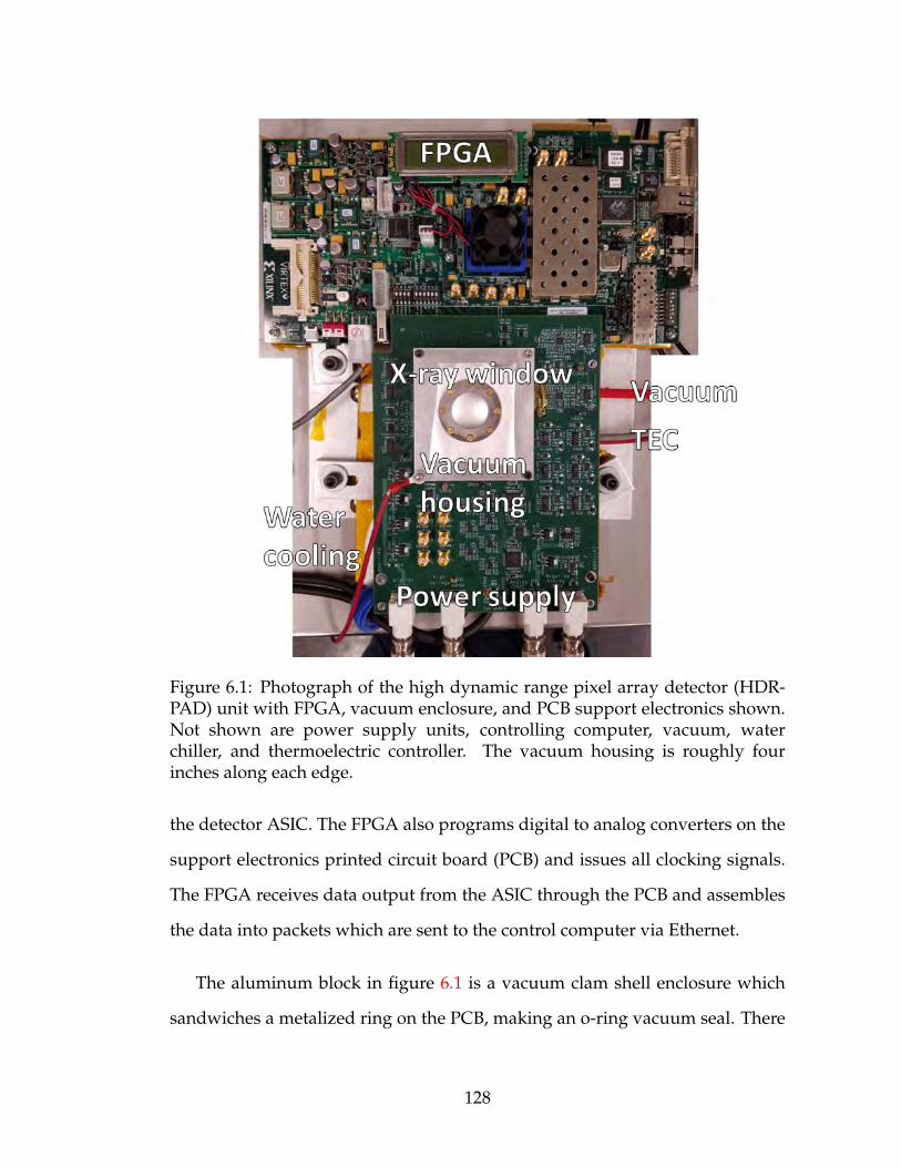
Figure 6.1: Photograph of the high dynamic range pixel array detector (HDR-PAD) unit with FPGA, vacuum enclosure, and PCB support electronics shown.Not shown are power supply units, controlling computer, vacuum, waterchiller, and thermoelectric controller. The vacuum housing is roughly fourinches along each edge.
the detector ASIC. The FPGA also programs digital to analog converters on the
support electronics printed circuit board (PCB) and issues all clocking signals.
The FPGA receives data output from the ASIC through the PCB and assembles
the data into packets which are sent to the control computer via Ethernet.
The aluminum block in figure 6.1 is a vacuum clam shell enclosure which
sandwiches a metalized ring on the PCB, making an o-ring vacuum seal. There
128
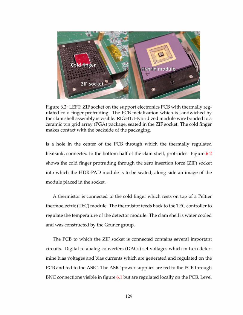
Figure 6.2: LEFT: ZIF socket on the support electronics PCB with thermally reg-ulated cold finger protruding. The PCB metalization which is sandwiched bythe clam shell assembly is visible. RIGHT: Hybridized module wire bonded to aceramic pin grid array (PGA) package, seated in the ZIF socket. The cold fingermakes contact with the backside of the packaging.
is a hole in the center of the PCB through which the thermally regulated
heatsink, connected to the bottom half of the clam shell, protrudes. Figure 6.2
shows the cold finger protruding through the zero insertion force (ZIF) socket
into which the HDR-PAD module is to be seated, along side an image of the
module placed in the socket.
A thermistor is connected to the cold finger which rests on top of a Peltier
thermoelectric (TEC) module. The thermistor feeds back to the TEC controller to
regulate the temperature of the detector module. The clam shell is water cooled
and was constructed by the Gruner group.
The PCB to which the ZIF socket is connected contains several important
circuits. Digital to analog converters (DACs) set voltages which in turn deter-
mine bias voltages and bias currents which are generated and regulated on the
PCB and fed to the ASIC. The ASIC power supplies are fed to the PCB through
BNC connections visible in figure 6.1 but are regulated locally on the PCB. Level
129

shifters buffer digital signals from the FPGA to the ASIC, including clock sig-
nals. The PCB also contains analog to digital converters (ADCs) which are con-
trolled by the FPGA. They receive analog data from the ASIC and send digital
conversions of the data to the FPGA to be recorded.
HDR-PAD ASICs were bonded to 500 µm thick silicon photodiodes fabri-
cated by SINTEF (Oslo, Norway). The diodes feature gold pad metalization
over p+ implantation on the ASIC bonding side. The x-ray entrance side is
coated with an aluminum metalization for bias voltage application over n+ im-
plantation. These diodes were originally developed for use with the MM-PAD
detector and more details can be found in Lucas Koerner’s dissertation in which
the same sensors were employed [74]. Because the ASIC studied here is the
product of a multi-project wafer fabrication, only diced ASICs could be pro-
cured and thus wafer-level bump bonding was not possible. To bond the sensor
to the ASIC, silver epoxy bumps were applied via stencil to pixel inputs and
gold studs were applied to pixel connections on the sensor. Flip-chip bonding
of the sensor and ASIC was then possible.2
Figure 6.3 is a photograph of a hybridized HDR-PAD module. The top most
layer is the 500 µm silicon sensor which is bonded pixel-by-pixel to the ASIC.
The ASIC is wire bonded to a ceramic pin grid array (PGA) package. All com-
munications to and from the ASIC are transmitted by the wire bonds. A single
wire bond can be seen connecting directly to the sensor layer. This wire bond
supplies the high voltage necessary to reverse bias the sensor layer. The high
voltage supply is connected through the PCB.
2The bonding procedure outlined here was performed by Jim Clayton of Polymer AssemblyTechnology, Inc. (Research Triangle Park, NC). At the time of the writing of this dissertation, alldocumentation related to this bump bonding are located on the Gruner group server “Peo-ple” in directory /us/Detectors-EssentialInformation/HDR-PAD/HDR-PAD_Sub2/stud_bonding_info/.
130

Figure 6.3: Close up image of a HDR-PAD hybrid module wire bonded to thePGA package. A single wire bond connects to the top surface of the sensorlayer to supply the reverse biasing voltage. The wire bond is made to a thickeraluminization which is visible along the edge of the sensor.
6.3 HDR-PAD ASIC
The HDR-PAD ASIC contains five pixel front-end variants with identical adap-
tive gain control circuitry, analog readout chains, digital readout chains, and
unified control signals. All pixels image simultaneously. Below the components
which are common to all pixels will be discussed after a brief overview of how
the pixels differ from the pixel front-ends described in Chapter 5.
131
6.3.1 Pixel overview
The five pixel variants fabricated on the HDR-PAD ASIC include two MM-PAD
2.0 variants, the charge dump oscillator, the capacitor flipping pixel, and a mod-
ification of the MM-PAD 2.0 pixel which will be referred to as the mixed mode
low drop out pixel (MM-LDO). The two MM-PAD 2.0 variants differ from each
other only in their total low gain integration capacitance. The front-ends of
these pixels have not changed substantially from the test structures included in
the first small scale fabrication described in Chapter 5. The CDO pixel has im-
plemented adaptive gain and the integrating amplifier has been replaced with
the same class AB amplifier as the capacitor flipping pixel uses. The capacitor
flipping pixel has implemented adaptive gain as well, and the level shifter uti-
lized in the dynamic thresholding scheme has been modified for lower power
consumption.
The LDO pixel is a clone of the MM-PAD 2.0 pixel, but the voltage which
determines the amount of charge removed with each charge removal execution
is controlled dynamically relative to the front-end. This dynamically adjusted
level is maintained by a low dropout regulator circuit which is capable of main-
taining a reference voltage over a wide range of input currents. Figure 6.4 is a
block level schematic of the LDO pixel. The level shifter used is the same as the
updated level shifter in the capacitor flipping pixel. The circuitry added to the
MM-PAD 2.0 framework maintains Vlow = V f ront−end − Vlevelshi f t. A current source
is required to bias the regulator and prevent Vlow from dropping to ground. The
transistor driven by the amplifier can be thought of as a variable resistor whose
impedance is adjusted to keep the input terminals of the operational amplifier
equal. The range of possible impedances is very large, and so the voltage on
132

this node can be maintained over a wide range of currents.
Figure 6.4: Simplified MM-LDO schematic. The pixel is identical to the MM-PAD 2.0, but rather than an externally supplied Vlow, the voltage is maintainedby a low dropout regulator circuit. The level of this voltage is set relative to thefront end.
The LDO modification is intended to benefit charge removal during very
high instantaneous flux. When the integrating amplifier is unable to maintain
Vre f on the front-end, the quantity of charge removed from the integration node
per capacitor switching execution, ∆Q = Crem(V f ront−end −Vlow), will vary from the
expected value, ∆Q = Crem(Vre f − Vlow). By setting Vlow relative to the front-end,
the quantity of charge removed should be more consistent: ∆Q = Crem(V f ront−end−
Vlow) = CremVlevelshi f t.
Table 6.1 summarizes the front end specifications of all five pixel variants.
133

Table 6.1: Pixel front-end specificationsPixel Chighgain [fF] Clowgain [fF] Crem [fF] Vre f − Vth [V]
MM-PAD 2.0 v1 40 880 880 0.5
MM-PAD 2.0 v2 40 2630 880 0.5
Charge dump oscillator 77 962 342 0.5
Capacitor flip 40 1000 1000 0.5
MM-LDO 40 880 880 0.5
6.3.2 Data readout
For the purposes of data readout, the chip is divided into four banks: MM-PAD
2.0, CDO, capacitor flipping pixels, and MM-LDO. The signals controlling each
bank are identical. Each bank uses identical but independent readout circuitry.
The banks take frames and read out signals in parallel.
Each pixel reports an analog value and a digital value. The analog value is
the output of the integrator, and the digital value is the output of the in-pixel
counter concatenated with a bit representing the gain state of the pixel. Analog
signals are converted to digital signals off-chip. Digitized analog values and
digital counts are sent to the FPGA, which controls all signaling to and from the
chip. The FPGA communicates with the controlling computer and sends all of
the values readout by the ASIC to the computer via Ethernet. The components
common to all pixels in the HDR-PAD, including the analog and digital readout
chains, are discussed below.
Digital readout chain
The gated oscillator in each pixel, which drives charge removal circuitry, also
connects to the input of an 18 bit in-pixel counter. The counter records the num-
134
ber of times charge removal occurs during an exposure. A global digital control
signal, referred to as STOP, prevents the in-pixel counters from incrementing
further and defines the end of an exposure from the perspective of the digital
components. The counter in each pixel is a ripple counter. Sufficient time for
signals to propagate through the counter is provided between the STOP signal
and the LATCH signal. The LATCH signal connects each in-pixel counter to a
column-wide shift register. The gain status bit in each pixel, discussed in the
next section, is also connected to the shift register and is readout in series with
the digital counts. The shift register in each pixel consists of 20 bits, 18 bits to
which the counter output is latched, one bit for the pixel gain status, and an
extra bit which is tied to the digital supply voltage. The pixel shift registers are
daisy-chained together to form one large, 320 bit shift register per column.
Once the digital values have been latched into the shift register, an externally
provided column select signal activates a digital multiplexer at the top of each
bank. The multiplexer connects the output of one shift register to a digital buffer
which transmits signals through a wire bond to a second digital buffer off-chip.
Each bank has its own multiplexer and dedicated chip-edge buffer so that all
four banks can be read out simultaneously. The banks all share the same column
select signal. The FPGA supplies a clock which shifts data out of the selected
column shift registers and to the FPGA for temporary storage. Once data from
all pixels in the selected column in each bank has reached the FPGA, the column
select signals switch and the next column is activated. Once all four columns in
each bank have been clocked out, digital readout is complete and all digital data
has been sent off chip.
135

Analog readout chain
All pixels in the HDR-PAD use identical but separate analog readout chains.
The analog output from each pixel integrator is monitored by an in-pixel sam-
ple and hold circuit. The pixel integrating amplifier drives the sample and hold
capacitor which is connected to the integrator output node by a switch. The
switch is controlled by a global digital signal. Opening the sample switch de-
fines the end of an exposure from the perspective of the analog data. This signal
is timed to coincide with the STOP signal which prevents the counter from in-
crementing. The switch is closed during integration such that the voltage on the
capacitor follows the integrator output. Once the switch is opened, the analog
value that will be read out is fixed.
The sample capacitor must be large enough that leakage current will not
have a significant impact on its voltage within the time scale of readout (mi-
croseconds). The sample capacitor must also be small enough to not have a
significant impact on the slew rate of the integrating amplifier. A value of 300 fF
was chosen based on the impact of this capacitive load on the integrating ampli-
fier in simulation. A five transistor differential amplifier connected in follower
configuration reads the sampled analog voltage and serves as the pixel analog
output buffer. The pixel analog output buffer was optimized for slew rate, set-
tling time, and noise. Noise in the analog buffer must be minimized to preserve
analog signal integrity. A five transistor differential amplifier topology pro-
vided the required specifications while minimizing power consumption. This
is a class A topology, so the maximum slew rate in one direction is roughly 10
times the maximum slew rate in the opposite direction. Fixed voltage offsets in
the buffer output are not detrimental to the operation of this amplifier as they
136

are trivially accounted for in calibration, so long as they do not push the ana-
log signal outside the functional range of the analog readout chain. Because
each pixel contains a pixel output buffer, power consumption must be kept low.
Here, quiescent current was kept below 5 µA. Rapid settling ensures that read-
out time can be minimized and frame rate maximized. The precise capacitive
load to be driven by this amplifier depends on the full chip layout, but a range
of values were explored to ensure proper performance. The pixel output buffer
is connected to a column bus via a second switch.
Figure 6.5 is a schematic of the analog readout chain from the sample and
hold to the chip edge. The column bus is a low impedance connection between
all pixels in a given column. Each column bus connects to the input of an-
other analog buffer, the column buffer. The column buffer output connects to
an analog multiplexer. The analog readout is orchestrated primarily by on-chip
circuitry which cycles through a fixed pattern of readout signals. After an ex-
ternally supplied initialization pulse, the analog readout signals increment with
each tick of a clock supplied by the FPGA. The signals cycled through are row
select and column select. Again, each bank reads out in parallel. A row select
signal connects all pixels in a given row to their respective column buses (clos-
ing the in-pixel switches connecting the sample and hold buffers to the column
buses), and a column select signal activates each column bus connection to the
multiplexer in succession. Once a row has been cycled through, the row select
increments and the column select signal repeats its cycle.
At the output of the multiplexer, a large class AB analog buffer sends analog
signals off-chip through a wire bond. Several class AB topologies were explored
for use at the chip edge. The capacitive load driven by this buffer is often on the
137

Figure 6.5: Simplified ASIC analog readout chain schematic. Sample and holdcircuits in each pixel connect to a column bus through a switch. A row selectsignal closes this switch and connects all sample and hold circuits in a given rowto the column bus. A buffer at the edge of the column bus feeds a multiplexer.A column select signal drives the multiplexer to connect each column buffer toan edge buffer in sequence. The edge buffer sends analog signals off-ship fordigitization. Each bank posesses its own copy of the depicted circuitry.
138

order of picofarads, depending on the wire bond pads, the wire bonds them-
selves, and the PCB-side analog buffers being driven. 5 pF and 20 pF loads
were used in simulation while evaluating various edge buffer designs. Because
the chip only contains one edge buffer per bank, performance is generally val-
ued over power consumption. Here we limited edge buffer quiescent current
to less than 500 µA. The final design had a quiescent current of 86 µA in simu-
lation. A settling time of 50 ns throughout the range of capacitive loads tested
was also required. Stability must be maintained throughout the entire range
of loads. Again, a fixed offset in output voltage does not impact performance
significantly, but noise added to the buffered signal must be minimized. The
chosen topology is based on the AB amplifier used for signal integration in pix-
els, as described in Chapter 5. The amplifier was modified for enhanced output
at the expense of gain. This amplifier provided the necessary slew rate and
output swing.
Once analog signals are buffered off chip, they reach another analog buffer.
This buffer, on the support PCB, is fully differential and feeds its output to an
analog to digital converter (ADC). Each bank has its own off-chip buffer, but
all four of the buffers share a common differential reference voltage. The ADCs
employed are dual channel, so there are two ADCs on the PCB, and each one
is shared by two banks. The analog to digital conversion gain is set by resistors
on the PCB. While the resistors are specified with high tolerance, the exact con-
version gain must be factored into calibrations. Once analog signals have been
digitized, the ADCs are clocked by the FPGA to output the digitized values. The
FPGA collects these data and sends them along with the counter output values
to the controlling computer via Ethernet.
139

6.3.3 Adaptive gain implementation
Each pixel’s gain state is controlled by an S-R latch circuit. The comparator
monitoring the integrator output in each pixel controls the sampling of the latch,
and the latch input is always high. When the comparator triggers, the latch
samples the input and sets its state to the input level. In this case, sampling
closes the adaptive gain switches and the pixel enters the low gain state.
In each pixel, the charge removal capacitor switching is controlled by an
AND logic gate. The inputs of the AND gate are the output of the compara-
tor and the output of the adaptive gain latch. A delay element, composed of
an inverter chain, sits in series between the latch output and the AND gate in-
put. This ensures that when adaptive gain is triggered by the comparator for
the first time in an exposure, the charge removal circuitry is not immediately
triggered as well. Rather, the adaptive gain pulls the integrator output above
the comparator threshold voltage before the charge removal is executed. Al-
ternatively, if there is sufficient input to keep the integrator output below the
threshold voltage in low gain, a charge removal event is required and will be
performed shortly after the gain switching.
The latch controlling the adaptive gain is also connected to the 19th bit of
the in-pixel shift register which reads out the in-pixel counter output. Because
knowledge of the adaptive gain state is required to interpret the analog output,
the gain state of each pixel in each exposure must be recorded and readout with
the analog and digital data. By tying the adaptive gain control signal to the shift
register, the gain state of the pixel front-end is readout along with the count of
charge removals and the end of each frame.
140
6.3.4 Programmable test sources
For functional testing, each pixel contains a programmable current source. The
current source consists of a PMOS transistor gated by a second PMOS transistor.
The gate voltage of the first transistor is set externally and determines the level
of input to the pixel. The source terminal is connected to the analog supply
voltage. The second transistor’s gate is set by a status bit stored in-pixel. The
status bit is set by a specific bit in the pixel’s shift register. The shift register bit
is written to the in-pixel memory when the digital signal WRITE is high and
the digital column select signal is also high. By reading in specific bit patterns
to the column shift register and activating column select, arbitrarily specified
pixel test sources can be activated.
While reusing the digital readout column select signal for programming in-
pixel current sources is efficient in reducing the number of wire bonds required
to operate the chip, it was found in testing that digital readout could at times
activate in-pixel test sources erroneously. Setting the default level of the WRITE
signal to low has helped to address this issue. However, the architecture should
be updated in future iterations.
To improve the functionality of the current source, the gate voltage of the
PMOS transistor should be set by a current mirror rather than a DAC. That
would permit a more controlled and predictable input to pixels. Additionally,
as will be seen in Chapter 7, the parasitic capacitance on the pixel front end is
quite large. In an effort to minimize this, the transistor gating the current source
should be as small as possible.
141
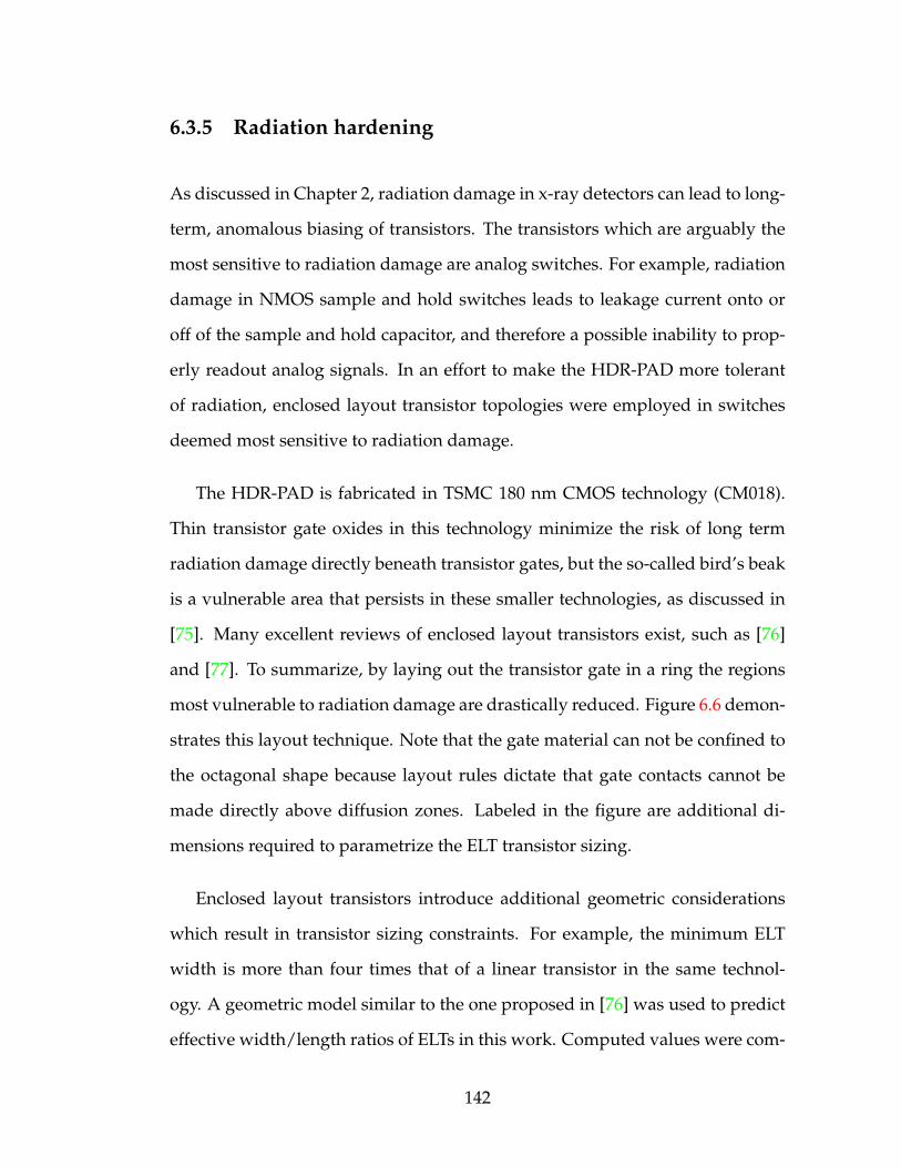
6.3.5 Radiation hardening
As discussed in Chapter 2, radiation damage in x-ray detectors can lead to long-
term, anomalous biasing of transistors. The transistors which are arguably the
most sensitive to radiation damage are analog switches. For example, radiation
damage in NMOS sample and hold switches leads to leakage current onto or
off of the sample and hold capacitor, and therefore a possible inability to prop-
erly readout analog signals. In an effort to make the HDR-PAD more tolerant
of radiation, enclosed layout transistor topologies were employed in switches
deemed most sensitive to radiation damage.
The HDR-PAD is fabricated in TSMC 180 nm CMOS technology (CM018).
Thin transistor gate oxides in this technology minimize the risk of long term
radiation damage directly beneath transistor gates, but the so-called bird’s beak
is a vulnerable area that persists in these smaller technologies, as discussed in
[75]. Many excellent reviews of enclosed layout transistors exist, such as [76]
and [77]. To summarize, by laying out the transistor gate in a ring the regions
most vulnerable to radiation damage are drastically reduced. Figure 6.6 demon-
strates this layout technique. Note that the gate material can not be confined to
the octagonal shape because layout rules dictate that gate contacts cannot be
made directly above diffusion zones. Labeled in the figure are additional di-
mensions required to parametrize the ELT transistor sizing.
Enclosed layout transistors introduce additional geometric considerations
which result in transistor sizing constraints. For example, the minimum ELT
width is more than four times that of a linear transistor in the same technol-
ogy. A geometric model similar to the one proposed in [76] was used to predict
effective width/length ratios of ELTs in this work. Computed values were com-
142

Figure 6.6: Schematic of an enclosed layout transistor (ELT) with source, gate,and drain terminal connections labeled. Additional dimensions are required toparametrize the transistor. Rather than simply a length and a width, two lengthsand two widths are required, labeled as L1, L2, a, and b where L’s are lengths.
pared to widths and lengths of ELTs extracted from layout and agreed well.
In this work, NMOS ELTs were used as sample and hold switches, pixel reset
switches, and adaptive gain switches. Each of these switches are sensitive to
leakage current.
These switches are all connected to capacitors which hold analog values,
and are therefore sensitive to charge injection. Charge injection through CMOS
switches, sometimes referred to as clock feed-through, can pose a serious prob-
lem to the fidelity of analog signals. The topic is discussed and modeled in [78–
80]. To summarize, as discussed in Chpater 2, a conductive channel forms be-
neath the gate of a transistor in saturation, as is the case when a CMOS switch is
closed. When the switch is suddenly opened, the charge which formed the chan-
nel must go somewhere. Because the channel to drain and channel to source
143

junctions are effectively forward biased, change injection into the substrate is
negligible and channel charge enters the source and drain nodes. Addition-
ally, the gate overlap capacitance with the source and drain form charge pumps
which are activated by switching signals.
If the source or drain are connected to nominally floating nodes, the charge
injection will affect the voltage on these nodes. This is a problems for integrating
detectors. In an effort to minimize the impact of charge injection, the dummy
switch technique was employed as described in [81]. In this scheme, two half-
size dummy switches are placed, one on either side of the active switch. The
dummy switches are the same type as the active switch and are shorted so that
they do not affect conduction in any way. They are driven by the compliment
of the active switching signal. Because the dummy switches are always making
a transition which is opposite the active switch, the charge that they inject is
the opposite of the charge injected by the active switch. Because their gate area
is half that of the active switch, the injected charge will be canceled provided
that the active switch charge injection is split evenly between the source and
drain. Figure 6.7 illustrates the concept of dummy switches for charge injection
compensation.
Note that the use of ELTs necessitates larger gate areas than would otherwise
be dictated by process design rules. This results in larger than average charge
injection, and thus the compensation provided by dummy switches is of greater
importance. The HDR-PAD uses especially large switches to deal with large
signals. How effective the dummy switch compensation is depends on several
factors. The ON impedance of the active switch, along with the rate of active
switch signal change, dictates the degree to which the two sides of the switch
144

Figure 6.7: Dummy switch compensation schematic. The active switch isflanked by two half-sized switches. The half sized switches are shorted so thatthey do not control any connections between nodes. They are driven by thecomplement of the active switching signal which results in opposite charge in-jection of the active switch. If the charge injected by the active switch is splitevenly between the nodes it connects, the net charge injection of each nodeshould be zero.
can equalize their respective voltages through channel conduction. Equal divi-
sion of injected charge between the source and drain is not guaranteed however.
The partitioning of charge between the source and drain of the active switch is
dependent on the relative capacitances of these nodes. If sharper clock edges
are used however, a more equal partitioning of charge can be achieved.
Perhaps the most confounding factor to be dealt with in regard to dummy
switch charge injection compensation in the HDR-PAD is the relative switch-
ing times of the active switch versus the dummy switches. This has a strong
effect on the ability to cancel injected charge, as discussed in [81]. In the HDR-
PAD, digital input signals from off-chip are buffered at the chip edge, and their
complement is generated alongside the buffered signal. This introduces an un-
avoidable delay between the two signals. The effect of charge injection from
switches will be examined more closely in Chapter 7. In future detectors, if
pin count is not problematic, digital signals and their complement can both be
generated off-ship, which would permit tweaking and fine-tuning of delays be-
145

tween them. If this is not possible, it may be beneficial to add delay circuitry to
the chip edge digital buffers which would minimize the delay between the two
signals.
146
CHAPTER 7
HDR-PAD CHARACTERIZATION
7.1 Introduction
Establishing basic functionality of the system takes considerable effort, but once
established, system performance must be evaluated. Below, the evaluation of
the HDR-PAD is described. Basic operating parameters are extracted from dark
current integration measurements and low flux x-ray exposure. Ultimately the
detector attempts to measure a direct synchrotron x-ray beam to test high flux
signal integration. The HDR-PAD in its present state does not have the sensitiv-
ity to small signals that was originally specified by the design goals, and con-
tributing factors to this are examined. The infrared laser used in the work de-
scribed in Chapter 4 became inoperable shortly after the pulse work concluded,
and so no tests of the HDR-PAD with very high instantaneous flux were per-
formed.
Performance of the MM-PAD 2.0 pixels, the capacitor flipping pixels, and the
MM-LDO pixels will be examined, but the CDO pixel operated inconsistently
and will therefore not be discussed. The analog output of the CDO pixel in any
frame with an integration time longer than ∼1 ms was at or above the highest
voltage measurable by the analog to digital converter. This implies that the
front-end integration node of the pixel reached a low value. This is supported
by the influence that this bank had on adjacent pixel columns. It can be seen
that pixels adjacent to the CDO bank received less signal than other pixels in
the same bank under constant external input. Some parameters of the CDO
pixel could be extracted, but due to lack of performance in most tests, there will
147

be no further discussion of the pixel in this chapter.
7.1.1 Dark current integration
To get a picture of the pixels’ overall performance and functionality, dark cur-
rent integration is a useful tool. Recall in Chapter 2, dark current from photo-
diode sensors was discussed. While the signal from the sensing layer itself is
often a nuisance, it can serve as a useful diagnostic. The dark current from the
sensor is a low level, relatively steady input.
By taking a series of frames with linearly increasing integration times, we
can track the pixel output as a function of input. Recall that dark current is ex-
ponential in temperature. Here the detector was held above room temperature
(at 30oC) and the sensor bias was raised to 110V, roughly 30V higher than the
bias required for sensor depletion. These factors increase the total dark current,
and therefore decrease the integration time required to initiate adaptive gain
and charge removal circuits.
Figure 7.1 depicts the output from an MM-PAD 2.0 pixel as a function of
exposure time. Similar plots were obtained for all pixel variants and all look
essentially the same. In these measurements, the CDO pixel output begins at
the expected level, but rises steadily to a maximum output over the course of
500 µs, indicating that the front end is approaching ground.
At first glance, the output plotted in figure 7.1 verifies that the pixel is in-
tegrating photocurrent as expected. The sensor is biased for hole collection, so
the output slews down in time. Once Vout = Vth, roughly 4800 ADU here, the
148

Figure 7.1: Average MM-PAD 2.0 pixel output as a function of exposure time.The pixel input is sensor dark current, which is relatively constant, so exposuretime corresponds linearly to total integrated signal. Basic operation of the pixelis evident. Positive charge accumulates on the integration node, causing theintegrator output to decrease in voltage. Once Vout = Vth (roughly 4800 ADU)the adaptive gain is triggered (at 50ms), and the pixel continues to integrate.When Vout = Vth again, charge removal occurs (first at 650ms).
adaptive gain is triggered. The output jumps back up and the integrator output
is pulled away from the threshold voltage. The pixel continues to integrate dark
current, but the slope of the line has changed indicating that the gain of the pixel
has changed. Subsequent approaches to the threshold voltage by the integrator
output result in output jumps which correspond to charge removal events, as
verified by the pixel digital output.
Dark current is integrated by all pixel simultaneously, and the measurements
provide a broad verification that the pixels are functioning as intended under
149

non-strenuous conditions. A lot of information can be pulled from these plots.
The switching point in ADU of each pixel can be extracted from these measure-
ments. Specifically, the ADU values at which adaptive gain/charge removal is
triggered, and the ADU value to which the pixel returns after either of these
events are needed to interpret pixel output. This is a direct measurement of ∆V,
the change in voltage which occurs on the integration node with each charge re-
moval event, which is essential to interpreting high signal measurements. Note
that the value of ∆V is only known in ADU at this point.
Furthermore, the ratio of the slopes of integration in high vs. low gain pro-
vide valuable information as well, assuming that the pixel input remains con-
stant in both states. These slopes allow the low and high gain to be calibrated
relative to eachother. Because the average input current is not a known quantity
in these measurements, the absolute gain can not be reliably pulled from these
frames. What we wish to know is the change in voltage (or ADU) of the output
as a function of input charge. To measure this empirically, we need a known
input. This is provided by x-rays as discussed in the next section.
Interestingly, the gain ratios obtained do not correspond exactly to the ratios
expected based on total integration capacitance. Instead, the ratios consistently
yielded numbers which imply a high gain integration capacitance closer to 60
fF in all pixels, rather than the 40 fF expected. This can be understood as an
effect of parasitic capacitance on the front end decreasing the charge collection
efficiency of the integrating amplifiers, as discussed in Chapter 2. The HDR-
PAD pixels each contain a protection diode which prevent the front end voltage
from rising significantly above the supply voltage. The diodes were intended to
protect pixels from damage that may occur with very high instantaneous flux
150

inputs. These diodes are quite large, as the pixels were intended to be tested
with XFEL like inputs. They may be contributing much of this parasitic capac-
itance, along with the detector sensor and bump bonds. Future pixels should
consider utilizing much smaller protection diodes to minimize this effect. If the
detector in question is not intended for use at XFELs, no protection diode may
be required at all.
7.1.2 Photon histograms
Another effective means of assessing a detector’s performance is with low flu-
ence exposure to radiation. After confirming that the HDR-PAD responds to
radiation as expected (initial tests were performed with exposure to americium
radiation), the HDR-PAD was mounted on a beamline in the Gruner lab to be
exposed to silver kα x-rays from a tube source. X-rays passed through a graphite
monochromator to select for the characteristic 22.16 keV x-rays.
Recall that x-rays absorbed on boundaries between pixels can split the
photo-generated charge between pixels. In this calibration, we would like to
deposit a known quantity of signal in a pixel. Even with a monochromated
source, charge sharing needs to be addressed. Here we used a tungsten mask
with an array of 75 µm holes with a 450 µm pitch to shield most pixels from ra-
diation. Pixel pitch on the HDR-PAD is 150 µm, so properly aligning the mask
with the pixels ensures that the nearest neighbors of illuminated pixels receive
no signal. Signal measured in illuminated pixels is generally not shared with
neighbors because the mask was positioned with mask holes centered on pix-
els, as depicted in figure 7.2.
151

Figure 7.2: Cartoon depiction of pinhole mask alignment. Pin holes are smallerthan pixels and spaced more than one pixel width apart. Aligning the pinholesover the center of pixels ensures that the signal from each photon absorbed bya pixel is not shared with neighboring pixels.
In this configuration, the signal received by illuminated pixels should arrive
in integer multiples of 22.16 keV, and the relative frequency of each multiple
should follow a Poisson distribution. Figure 7.3 is a histogram of 25,000 analog
outputs from a single MM-LDO pixel on the HDR-PAD with 1 ms exposure
times. The data has been reversed such that decreases in output correspond
to increases in ADU. Plotted on top of this histogram is a fit incorporating the
constraints indicated by our knowledge of the system.
The fitted function is the sum of some number of Gaussian functions, in this
152

Figure 7.3: Histogram of 25,000 analog outputs from an MM-LDO pixel withlow flux silver kα radiation. Exposure time was 1 ms. The histogram is fit by asum of five Gaussian functions. Parameters from the fit describe the pixel’s gainand noise characteristics. Peaks corresponding to integer numbers of photonsabsorbed by the pixel in the integration window are labeled.
case five:
f it = Σ4n=0x4e−x3
xn3
n!exp
(−(nx2 − ADU + x5)2
2x21
). (7.1)
Each Gaussian corresponds to an integer number of photons arriving at the
pixel within the integration window. Each Gaussian has the same width, which
corresponds to the variability in the output of the detector. This width is a fit
parameter (x1) that provides a measure of overall noise in the analog data chain.
The Gaussians are evenly spaced. The space between Gaussians is the signal
generated by one 22.16 keV x-ray in ADU. This is a fit parameter (x2) and is an
absolute measure of the pixel’s analog gain. The relative heights of the Gaus-
153
sians follow a Poisson distribution described by a fit parameter (x3). This param-
eter describes the average flux incident on the pixel in question. Fit parameter x4
is effectively a normalization corresponding to the number of frames contribut-
ing to the histogram, and x5 is an offset equivalent to background subtraction.
In this case five Gaussian functions were fit to the histogram because there
were not an appreciable number of occurrences of more than four photons inci-
dent on the pixel within the integration window, but in higher flux data sets the
sum extends to higher numbers. The first peak in the histogram corresponds
to zero integrated photons. The width of this Gaussian is roughly equal to the
others, confirming that the vast majority of analog signal variation originates in
the detector itself.
Photon histograms were obtained for pixels in all banks and were analyzed
in the manner described above. Table 7.1 summarizes the pixel data extracted
from photon histograms. The ADU/keV figure is the total effective gain of the
analog signal chain when the pixel is in high gain mode, including effects from
the analog buffer chain and the off-chip ADC. This number is the absolute mea-
surement of pixel gain required to utilize the slope ratio discussed in the previ-
ous section. For example, in high gain the MM-PAD 2.0 pixel out changes by
13.29 ADU per keV of signal incident, so an 8 keV x-ray will change the output
by 106.32 ADU on average. The ratio of high gain to low gain constant cur-
rent integration slopes from the previous section is 15.1, which implies that an
8 keV x-ray will change the output of the MM-LDO pixel output by ∼7 ADU on
average in low gain.
σ f it is the fit parameter x1 and characterizes the variability of the analog out-
put. The number is listed in ADU and keV (utilizing the extracted gain). The
154

Table 7.1: Parameters extracted from photon histogramsPixel Gain [ADU/keV] σ f it [ADU] σ f it [keV]
MM-PAD 2.0 13.05 72.0 5.51
Capacitor flip 7.67 56.8 7.40
MM-LDO 13.29 72.9 5.48
σ f it in keV indicates that the signal to noise ratio of a single 8 keV x-ray is not
much larger than one. While measurements can still be made with 8 keV x-rays,
the rate of false positive events in the single photon signal regime is greater than
desired, 1.46 in the case of the MM-LDO pixels. For the sake of comparison, the
original MM-PAD detector achieves a signal to noise ratio of ∼6 for 8 keV x-ray
inputs, which corresponds to a false positive count rate of less than one in one
hundred million. The noise of the HDR-PAD has been improved since these
measurements were taken, but the design specifications were not met in this
regard. The final section of this chapter is dedicated to exploring this issue.
As an additional verification of pixel functionality, figure 7.4 compiles pho-
ton histograms from a set of MM-LDO pixels with progressively higher flux. In-
dividual photon resolution at 22.16 keV is maintained up to the point at which
the adaptive gain circuitry activates. The full well in high gain, or the quantity
of charge required to initiate the gain switch, matches the expected value.
7.1.3 High flux measurements
Having verified basic functionality of the detector and extracted parameters
from the dark current integration and low flux x-ray integration, The HDR-PAD
must be tested with a high flux input. Working with Jacob Ruff from CHESS
155
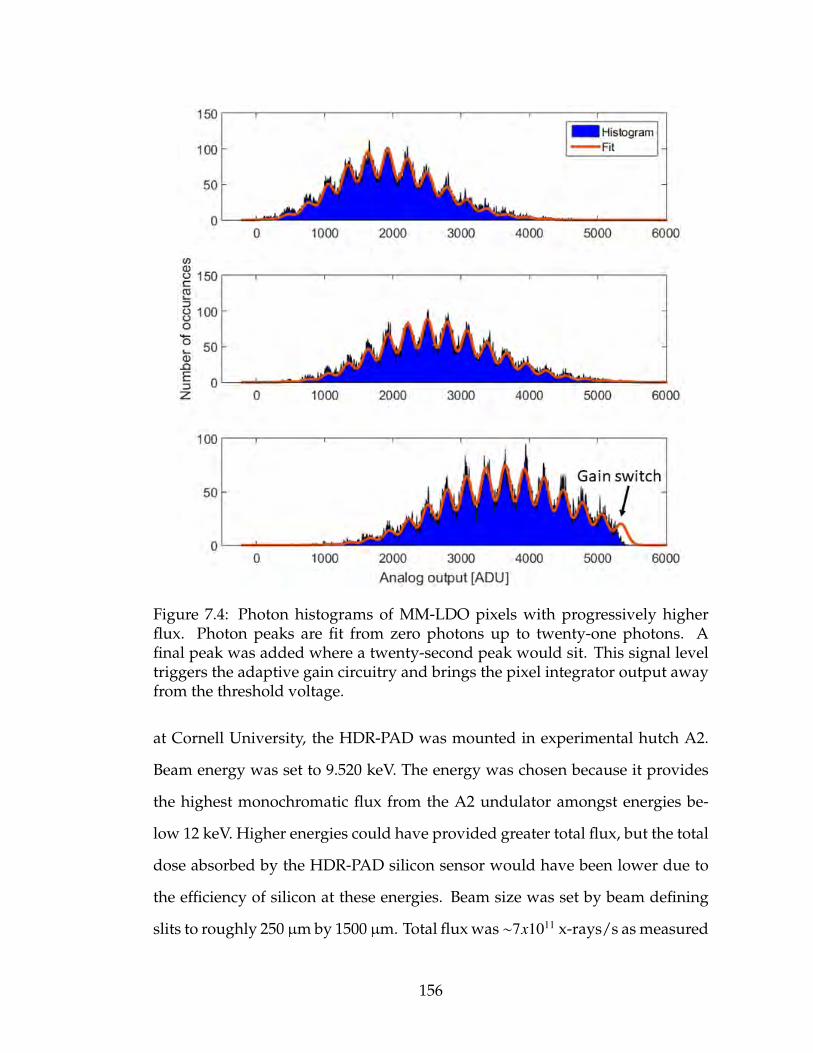
Figure 7.4: Photon histograms of MM-LDO pixels with progressively higherflux. Photon peaks are fit from zero photons up to twenty-one photons. Afinal peak was added where a twenty-second peak would sit. This signal leveltriggers the adaptive gain circuitry and brings the pixel integrator output awayfrom the threshold voltage.
at Cornell University, the HDR-PAD was mounted in experimental hutch A2.
Beam energy was set to 9.520 keV. The energy was chosen because it provides
the highest monochromatic flux from the A2 undulator amongst energies be-
low 12 keV. Higher energies could have provided greater total flux, but the total
dose absorbed by the HDR-PAD silicon sensor would have been lower due to
the efficiency of silicon at these energies. Beam size was set by beam defining
slits to roughly 250 µm by 1500 µm. Total flux was ∼7x10¹¹ x-rays/s as measured
156
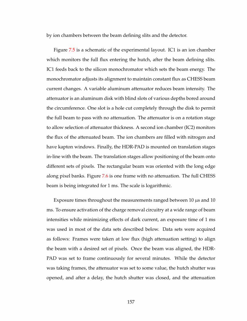
by ion chambers between the beam defining slits and the detector.
Figure 7.5 is a schematic of the experimental layout. IC1 is an ion chamber
which monitors the full flux entering the hutch, after the beam defining slits.
IC1 feeds back to the silicon monochromator which sets the beam energy. The
monochromator adjusts its alignment to maintain constant flux as CHESS beam
current changes. A variable aluminum attenuator reduces beam intensity. The
attenuator is an aluminum disk with blind slots of various depths bored around
the circumference. One slot is a hole cut completely through the disk to permit
the full beam to pass with no attenuation. The attenuator is on a rotation stage
to allow selection of attenuator thickness. A second ion chamber (IC2) monitors
the flux of the attenuated beam. The ion chambers are filled with nitrogen and
have kapton windows. Finally, the HDR-PAD is mounted on translation stages
in-line with the beam. The translation stages allow positioning of the beam onto
different sets of pixels. The rectangular beam was oriented with the long edge
along pixel banks. Figure 7.6 is one frame with no attenuation. The full CHESS
beam is being integrated for 1 ms. The scale is logarithmic.
Exposure times throughout the measurements ranged between 10 µs and 10
ms. To ensure activation of the charge removal circuitry at a wide range of beam
intensities while minimizing effects of dark current, an exposure time of 1 ms
was used in most of the data sets described below. Data sets were acquired
as follows: Frames were taken at low flux (high attenuation setting) to align
the beam with a desired set of pixels. Once the beam was aligned, the HDR-
PAD was set to frame continuously for several minutes. While the detector
was taking frames, the attenuator was set to some value, the hutch shutter was
opened, and after a delay, the hutch shutter was closed, and the attenuation
157

Figure 7.5: CHESS A2 beamline schematic. Beam enters the hutch through beamdefining slits and enters the first ion chamber (IC1) which measures the fullbeam flux. A variable attenuator rotates to place aluminum of various thick-nesses in the path of the beam. A second ion chamber (IC2) measures the atten-uated flux. The attenuated beam strikes the HDR-PAD directly.
Figure 7.6: Sample image with 1 ms exposure to the full A2 beam. The scale islogarithmic.
158

setting was incremented. In this way, dark frames are acquired between each
set of exposures.
Each bank was subjected to the full range of x-ray flux available, more than
five orders of magnitude range. Flux on the peak pixel was calculated. Flux on
the entire bank was also calculated. The fraction of total signal measured by the
detector versus the signal of the brightest pixel was computed and used to scale
the independently measured total attenuated flux incident on the chip. Plotted
below are the signals as measured by the HDR-PAD pixels versus the signal as
measured by the ion chambers, scaled by the calculated fraction. The error bars
are the standard deviation of measurments at each flux based on the frames
aquired (generally about 50 frames per data point). An orange dashed line is
included for comparison which is the flux as measures by the ion chambers
versus itself, a line of slope one, representing perfect performance.
Figure 7.7: Signal measured by the MM-PAD 2.0 pixel with a total integrationcapacitance of 880 fF versus the signal measured by ion chambers. The dashedline represents perfect performance for comparison.
159

Figure 7.7 plots the flux measured by the MM-PAD 2.0 v1 pixel (v1 corre-
sponds to Cint = 880 fF). The pixel performs extremely well, and little deviation
from the expected behavior is observed.
Figure 7.8: Signal measured by the MM-PAD 2.0 pixel with a total integrationcapacitance of 2630 fF versus the signal measured by ion chambers. The dashedline represents perfect performance for comparison.
Figure 7.8 plots the MM-PAD 2.0 v2 pixel measurements (v2 corresponds to
Cint = 2630 fF). Here the measurements are systematically over estimating the
incident flux. The most likely explanation is a slight miscalibration. The ADU to
keV ratio used to interpret these data was extracted from the dark current inte-
gration and photon histogram measurements discussed above. Because the de-
tector response is so linear, it seems unlikely that the pixels are malfunctioning.
The value which represents the number of x-rays removed from the integration
node with each capacitor switching event may be less than the original calibra-
tion implied. A more careful calibration of the pixel response would most likely
yield better agreement between the measured input and the actual input.
160
Figure 7.9: Signal measured by the capacitor flipping pixel with an externallysupplied threshold voltage versus the signal measured by ion chambers. Thedashed line represents perfect performance for comparison.
Figure 7.9 plots the response of the capacitor flipping pixel with an externally
supplied threshold voltage. It also exhibits very linear performance. Measured
signal at the high flux end begins to dip. It is unclear whether this is a delay
induced error, as was explored in Chapter 5, or simply a slight miscalibration of
the pixel response. In either case, the pixel would benefit from further calibra-
tion, but performs well within the tested rage of flux.
Figure 7.10 plots the capacitor flipping pixel response with dynamic thresh-
olding activated. Here a clear drop off in response is seen, and the performance
is actually worse than in the externally thresholded case. The reason for this is
most likely poor performance of the level shifting circuit. Even in low fluence
testing, the circuit exhibited a tendency to switch sporadically, possibly due to
a sensitivity to transients. The level shifter may require supplementary reset
signals for optimal performance, but these have not been fully implemented.
161

Figure 7.10: Signal measured by the capacitor flipping pixel with dynamicthresholding enabled versus the signal measured by ion chambers. The dashedline represents perfect performance for comparison.
Figure 7.11: Signal measured by the MM-LDO pixel versus the signal measuredby ion chambers. The dashed line represents perfect performance for compari-son.
162
Finally, Figure 7.11 plots the response of the LDO pixel. While the response
does appear linear, the slope of the measured input is consistently less than one.
This is most likely due to an inadequate calibration of the low gain ADU to keV
ratio.
Note that while the input to the pixels should be fairly constant, there are
variations in beam flux throughout the course of measurement. Some of the
uncertainty in the measured inputs can be attributed to these fluctuations. The
beam intensity was stabilized by ion chamber feedback on the monochroma-
tor, but ion chamber measurements bring their own uncertainties, and feedback
systems have characteristic time scales over which they operate. Overall, the
system would benefit from further calibration and refinement of data interpre-
tation. The parameters used to interpret these data were obtained empirically,
but some refinement of calibration data could yield better results. Even so, the
detector responds well to a very wide range of signals, through the full five or-
ders of magnitude tested, up to 1010 9.52 keV x-rays per pixel per second. The
MM-PAD 2.0 pixel architecture demonstrates the most reliable performance.
7.2 Small signal resolution
The photon histogram data indicated that the signal to noise ratio of HDR-PAD
pixels with signals generated by single 8 keV x-rays is unsatisfactory. In contrast
to the well defined, separate peaks in figure 7.3, an analogous plot with 8 keV
x-rays would feature Gaussian curves which are only distinguishably separate
at their peaks, if at all. As discussed in Chapter 2, noise sources in detectors are
abundant, but we can perform tests to identify the dominant sources.
163

Figure 7.12: Pixel bank average versus pixel bank average. Each point repre-sents one frame. Bank averages from within the same frame are compared.Correlation coefficient is computed.
7.2.1 Global noise sources
To begin, some noise sources are global, while others are local to pixels. Another
way to say this is that some portion of the variability in pixel output is common
to all pixels, while another portion differs from pixel to pixel. Figure 7.12 is a
simple illustration of this phenomenon. Each point in the plots represents one
frame. The horizontal position is dictated by the average analog output value of
one bank of pixels, and the vertical position is the average analog output value
of another bank of pixels. Exposure time was 10 µs, kept low to minimize the
effect of dark current on the measurement.
A clear correlation is seen between banks. The MM-PAD 2.0 bank and the
MM-LDO bank are strongly correlated. This is to be expected because the pixel
architectures are nearly identical, and so global noise sources are likely to affect
these pixels in a similar way. Global noise sources include power supply and
bias fluctuations, as well as pick up from external sources, among others. These
will be investigated in turn. First we might ask what fraction of the pixel noise
164

can be attributed to global fluctuations?
If pixel noise were entirely independent between pixels, i.e., there are no
global fluctuations, an average of many pixels should vary less from frame to
frame than a single pixel output varies between frames. More rigorously, the
variance of the mean of a set of pixels in time is
Var(ΣN
i=1xi
N
)=
1N2
[ΣN
i=1Var (xi) + ΣNi, jCov
(xi, x j
)](7.2)
Where i and j index the pixels in the set to be averaged, Var is the variance of the
values over time, and Cov is the covariance of the values over time. Note that
the covariance of a variable with itself is equal to its variance. If the pixels lack
any correlation, i.e., their covariance is zero, the variance of the mean of pixels
should equal the sum of the individual variances divided by N2, or equivalently
the mean of the variances divided by N.
Figure 7.13 looks at this comparison. Standard deviations are plotted rather
than the variances in equation 7.2 to make a clearer connection to equivalent
noise charge. A set of 10,000 frames with 10 µs exposure time were acquired.
In each frame, N MM-PAD 2.0 pixels were selected and averaged together. The
standard deviation of the average value throughout the data set is plotted with
a blue dotted line. The variance of the output of each of the individual pixels
in the data set is also computed, and the variances are averaged and divided by
N. This is repeated 5000 times for each N and the square root of overall average
results is plotted. To reiterate, this plot compares the standard deviation of an
average:
dotted =
√Var
(ΣN
i=1xi
N
), (7.3)
versus the square root of the average of individual variances divided by N:
dashed =
√1
N2 ΣNi=1Var (xi). (7.4)
165

Figure 7.13: The standard deviation of N pixels averaged together is plotted asa blue dotted line. The average standard deviation of N pixels divided by N isplotted as an orange dashed line. If there were no global noise, the standard de-viation of the average value of many pixels would approach zero as N increases.
For independent random variables xi, every term in the covariance sum is
zero. The orange dashed line approaches zero as 1√
Nwhile the blue dotted line
approaches the standard deviation of the global noise.
Where does this global noise come from? To simultaneously assess the vari-
ability of power supplies and bias voltages along with analog to digital con-
version noise, the chip was removed from the ZIF socket and power supplies
and bias voltages were connected directly to analog output channels in the ZIF
socket, which feed to the ADC inputs. For supply voltages outside the nor-
mal range of ADC operation, the supply was connected to the output channel
through a resistive bridge consisting of two 1000 Ω resistors to ground. This
166

places a load on the supplies which is within their normal operating range. By
sending frame commands to the FPGA while the PCB is wired in this config-
uration, the ADCs will continuously digitize the voltage at their input. This
provides a measure of both fluctuations in supply/bias voltages and variability
in analog to digital conversion.
If the result of this test were very high variability, further steps would be re-
quired to disentangle the source of the variance. However, what was discovered
was a clear, high frequency fluctuation in the supply voltages, but not the bias
voltages. This indicates that there is noise on the power supply lines, but the
ADCs are operating reasonably well. It was discovered that the capacitors con-
nected to the power regulators on the PCB had a lower equivalent series resis-
tance than what is required by the regulators for stability. After replacing these
capacitors, the digital supply line was the only noisy line remaining. Replacing
the FPGA switching power supply with a linear power supply unit aided the
reduction of this variability drastically. Table 7.2 lists the standard deviation of
power supply and bias voltage analog to digital conversion values after these
changes. These measurements suggest the degree to which power supply fluc-
tuations might affect the variability of frame data from the ASIC, though the
actual impact is most likely smaller than the figures themselves.
Note that in this configuration, the power supplies are not loaded dynam-
ically, as they would be in actual operation. As a result, power supply droop
resulting from changing current draw by the ASIC can not be diagnosed in this
way.
To assess whether noise on the digital line is originating on the supply side
or ground side, the measurements above were repeated with the analog power
167

Table 7.2: Power supply variabilitySupply σ [ADU]
MM-PAD 2.0 Vre f 2.21
Charge dump oscillator Vre f 1.98
Capacitor flip Vre f 1.25
MM-LDO Vre f 2.69
Analog supply voltage 1.50
Digital supply voltage 12.89
supply connected through the resistive divider to digital ground and with the
digital power supply connected to analog ground. This crossing yielded stan-
dard deviations on both supplies of ∼6.5 ADU, suggesting that the problem is
not solely on either the supply or ground side. Rather, it is more likely that a
digital component on the FPGA or PCB is generating fluctuations on both.
Finally, noise contributions of the Peltier thermoelectric used to regulate the
temperature of the ASIC were assessed by imaging at room temperature with
and without the Peltier turned on. Significant pickup was measured with the
Peltier activated, though the noise was reasonably well addressed with a de-
bounce algorithm.
In general, global noise can be mitigated with a so called debounce algo-
rithm. By averaging the value of pixels which recieve no external signal in a
given frame, an estimate of the global noise is obtained. This value can then be
subtracted from all pixels to remove the global component of noise on a frame-
by-frame basis. While this technique was employed to address the remaining
global noise in the HDR-PAD, its effectiveness was limited due to the variety of
pixels in the pixel array. In any given frame, the number of pixels of a specific
architecture which receive no signal is small, and so the estimation of the global
168

noise is poor.
7.2.2 Local noise
After accounting for chip-wide noise sources, which primarily originate off-chip
and can therefore be addressed as discussed in section 7.2.1, the noise level of
the pixels still does not provide a satisfactory signal to noise ratio for a single
8 keV x-ray. Several imaging modes can be utilized to locate the source of the
signal variability. For example, the pixel can be read out continuously while
the pixel reset signal is held high. In reference to figure 6.4, the switch labeled
RST, which connects the input and output of the integrating amplifier, remains
closed throughout the entirety of framing rather than being opened to permit
the accumulation of charge by the pixel. In this configuration, the integrating
amplifier output follows Vre f . This was verified by sweeping the value of Vre f
and confirming that the output changed correspondingly.
With the reset signal held high, noise contributions from before the sample
and hold amplifier are minimized. Other than noise on Vre f itself, which was
shown above to be quite low, the amplifier output should be relatively constant.
Pixel output standard deviation in this configuration are displayed in table 7.3.
These figures are debounced bank averages.
Table 7.3: Pixel noise in resetPixel σ [ADU] σ [keV]
MM-PAD 2.0 12.11 0.93
Charge dump oscillator 22.74 2.81
Capacitor flip 13.02 1.70
MM-LDO 11.72 0.88
169

Table 7.4: Pixel noise in low gainPixel Clow [fF] σraw [ADU] σdebounced [ADU] σdebounced [keV]
MM-PAD 2.0 v1 880 15.20 13.25 22.35
MM-PAD 2.0 v2 2630 15.47 13.38 67.45
CDO 962 17.29 15.70 24.31
Capacitor flip 1000 29.43 14.87 48.48
MM-LDO 880 16.48 14.12 23.38
This indicates that noise contributions from the analog readout chain noise
are not dominating the pixel output noise. These values are sufficiently low
to obtain the desired signal to noise ratio in framing. Evidently the dominant
noise sources are on the front end. Another imaging mode consists of framing
with pixel gain starting low and staying low. I.e. the adaptive gain is forced
to activate before framing has begun. By increasing the integration capacitance,
we may be able to distinguish between a charge injection noise and a voltage
noise. A voltage noise on the front end would be seen as a larger equivalent
noise charge when integration capacitance is increased, while a charge injection
noise should present roughly the same equivalent noise charge in high and low
gain. Table 7.4 summarizes the findings. The table lists the standard deviations
of banks before and after debouncing. Each half of the MM-PAD 2.0 bank is
treated separately because their total low gain capacitances are different.
Here we see that the noise in low gain is very similar to that of the pixel in
reset. By comparison, the noise values extracted from the photon histograms,
listed in table 7.1, are significantly higher in ADU. This suggests that the pixel
noise is dominated by some form of charge injection which is particularly prob-
lematic in high gain mode. There is of course some voltage noise as well, as
evidenced by the higher equivalent noise change in low gain, but the drastically
170

reduced noise in terms of ADU imply that charge injection dominates. Rela-
tively large switches were employed in the layout of the HDR-PAD and are a
likely candidate for the source of charge injection noise. A rough calculation of
the charge that may be injected by such switches follows.
The reset switch in the MM-PAD 2.0 has a width of 6.0 µm, a length of 0.36
µm, and a multiplicity of two. It is flanked by two dummy switches as described
in a previous section, each with the same width and length but multiplicity of
one. Based on TSMC 180 nm process parameters, the gate oxide capacitance of
the reset switch is Cox =8.68 fF/µm2. The total gate capacitance of the active
reset switch is then
Cgate = 2wlCox. (7.5)
The reset signal swings from 1.8 V to 0 V. If we make the simplifying assump-
tions that the reset signal swing is fast enough to split injected charge evenly
between the front end and the analog output node, and further assume that
variations in the quantity of charge injected follows Poisson statistics, the stan-
dard deviation of the charge injected to the front end by the reset switch is
σQin j =√
wlCox∆V = 649e− (7.6)
in number of electrons. The dummy switch on the front end will inject a quan-
tity of charge from a distribution with the same standard deviation, so the total
uncertainty in the quantity of charge injected onto the front end, when these
quantities combine, is the standard deviation in equation 7.6 multiplied by√
2
because the uncertainties add in quadrature. The total uncertainty due to this
injected charge is equivalent to ∼3.3 keV signal charge. Note that gate-source
and gate-drain capacitances have been neglected.
The calculation above makes several simplifying assumptions, but serves
171
to illustrate that charge injection from the large switches used to reset the pix-
els could plausibly be the dominant noise source in HDR-PAD measurements.
Large reset switches were employed in the HDR-PAD for handling large signals
and resetting the pixels quickly. In simulation, the dummy switches canceled
out injected charge very well. It may be that the clocking patterns used in the
HDR-PAD can be refined to minimize the charge injection problem, and the
switches will actually work to within the design specification. However, more
testing and FPGA reprogramming is required.
The figures in table 7.4 also provide an opportunity to verify that the un-
certainty of signals which are just large enough to trigger adaptive gain will be
measurable with the desired signal to noise ratio. As verified in the high gain
photon histograms, roughly 49 8 keV x-rays are sufficient to trigger the MM-
PAD 2.0 adaptive gain. Poisson statistics dictate that a measured signal of 49 8
keV x-rays has an inherent uncertainty of ±7 x-rays. The noise figures in table
7.4 suggest that the uncertainty of a signal in low gain is below this level in all
pixels except the MM-PAD 2.0 pixels with a low gain integration capacitance
of 2630 fF. If the uncertainty due to the detector is below the uncertainty due
to shot noise, the total uncertainty of the measurement is near the experimental
minimum, the square root of the measured signal, because the uncertainties add
in quadrature. From this we can conclude that a low gain capacitance of 2630 fF
is too low with a high gain integration capacitance of 40 fF. To employ this low
gain capacitance and still resolve intermediate signals, a third gain stage would
be required. However, the low gain capacitances of 880 fF and 1000 fF are small
enough to provide Poisson limited measurements of intermediate signals.
172

CHAPTER 8
CONCLUSIONS
Throughout the course of this dissertation, the need for high dynamic range
x-ray detectors at high brightness light sources and the case for developing inte-
grating detectors to meet these needs was demonstrated. Integrating detectors
are possibly the only detector architecture which can adequately utilize the ca-
pabilities of x-ray free electron lasers, and enhanced flux at third generation
synchrotron sources cannot be fully utilized with other technologies, such as
photon counting detectors.
The use of a high dynamic range integrating detector, the MM-PAD, in
pulsed magnetic field studies at the Advanced Photon Source at Argonne Na-
tional Lab serves to illustrate the importance of further developing this technol-
ogy. The studies of Uranium dioxide are on-going, and evidence of its piezo-
magnetic properties on the atomic scale are being dissected. Further studies
are required to draw firm conclusions, but the addition of magnetic field direc-
tion switching to these studies promises to shed light on the question of how
piezomagnetism might arise from unit cell distortions.
The plasma effect in silicon diodes was investigated by simulating the
electron-hole pair clouds generated by XFEL-like scatter with a pulse infrared
laser. The results of these studies suggest that charge accumulation in detector
pixels stretches to longer time scales than expected due to plasma effects in high
density electron-hole pair clouds created in the sensors. These time scales can
reach over 1 µs, which is sufficient time for charge removal circuits to provide a
meaningful increase to the achievable dynamic range of an integrating pixel.
173

An initial small scale fabrication of pixel prototype front-ends demonstrated
the potential benefit of combining adaptive gain with charge removal tech-
niques. These integrating frameworks were evaluated with direct current in-
jection, and results suggest that they may be capable of integrating continuous
x-ray fluxes greater than 1011 8 keV x-rays/pixel/s. The pixel front-ends were
developed into fully functional pixels with mixed analog and digital readout. A
composite detector consisting of five different pixel architectures was designed
which would provide a platform for imaging with and evaluating the perfor-
mance of all pixel architectures simultaneously.
Fabrication of a 16x16 pixel hybrid detector, development of support hard-
ware and electronics, and refinement of operation resulted in a fully functional
hybrix pixel array detector utilizing the prototype front-ends and demonstrated
the functionality of the adaptive gain-charge removal combination in measur-
ing high flux x-ray radiation. This culminated in successful measurements of an
unattenuated x-ray beam at CHESS with a total flux greater than 1011 9.52 keV
x-rays/s spread over roughly twenty pixels.
By comparison, the measurements taken at CHESS represent a two order
of magnitude improvement over the original MM-PAD in sustained integrated
flux. The HDR-PAD may be able to integrate even higher fluxes, but this was
the highest flux available for testing in this experiment. Detectors such as the
AGIPD can integrate an average flux of this magnitude, but will saturate af-
ter roughly a microsecond. Here the HDR-PAD integrates 1000 times longer
than that and does not come close to saturation. Because the CHESS beam is
pulsed, the instantaneous flux on the target pixels is substantially higher than
1010 9.52 keV x-rays/pixel/s. Photon counting detectors such as the PILATUS3,
174

even with re-triggering circuitry to account for pileup, would experience signif-
icant non-linearities when measuring a beam with one one-thousandth of the
intensity measured here. The architectures tested in the HDR-PAD provide a
solid foundation on which to build future detectors, but some lessons should be
carried forward.
One significant shortcoming of the HDR-PAD is lack of small signal resolu-
tion. Specifically, the HDR-PAD does not achieve the target signal to noise ratio
for a signal of one 8 keV x-ray. The most likely cause of this is charge injection
due to large reset switches on the pixel front-ends. While large switches may be
required for rapid reset in high frame rate experiments, smaller switches would
likely suffice. Dummy switches were employed in the HDR-PAD to reduce the
magnitude of charge injection, and while seem to be achieving this goal, they
also add to the total variability of the detector output. With smaller switches,
the magnitude of charge injection would also be smaller and dummy switch
charge injection compensation might not be needed at all.
Dummy switches might still be employed if their timing can be controlled
independently of the active switches. In future detectors, these signals should
be controlled separately to permit fine-tuning of their relative behavior. Alter-
natively, greater care should be taken to match delays on each signal induced
by chip-edge buffers.
The test current source in each pixel of the HDR-PAD was invaluable in de-
bugging the detector operation. Bit shifts and shuffling of data were identified
with their use, and they should absolutely be included in future detectors. How-
ever, the erratic turning-on of the test source gating did prove to be a nuisance.
This behavior can be rectified by the addition of dedicated control signals for
175

writing to the in-pixel memory bits. Additionally, the current test source out-
put level should be controlled by a current mirror in future chips, rather than
an externally defined voltage. While the precision of a test source feeding the
integration node of an integrating pixel will never be ideal, this would permit
more linear changes in input strength, and would make performing some tests
much easier with little downside.
The pixel front-end parasitic capacitance in the HDR-PAD was larger than
expected. The current test source is one contributing factor to this capacitance,
but another source of this which can be addressed is the protection diode which
connects to the supply voltage included on the front-end of each pixel. While
some measure of protection should be included in a detector intended for use
at XFELs, the smallest possible diode should be used. The oversized switches
of the HDR-PAD are certainly another contributor to the parasitic capacitance
on the front-end node. Reducing this capacitance will improve the small signal
resolution of the pixels provided that charge injection is not the dominant noise
source.
Despite these shortcomings, the HDR-PAD represents a step forward in the
evolution of high dynamic range integrating detectors. The technology is ver-
satile, and a version of the detector presented here is being adapted for use with
electron microscopes, where the high dynamic range combined with area reso-
lution will continue to expand experimental opportunities.
176

APPENDIX A
LASER PULSE MEASUREMENT SCHEMATICS
Appendix A contains schematics for the printed circuit boards used to measure
infrared laser pulses as discussed in Chapter 4. Figure A.1 is the layout of the
printed circuit board to which the custom diode was connected. All PCBs in
this appendix were designed by Dr. Julian Becker during his time in the Gruner
Group at Cornell University.
Figure A.1: Layout of sample PCB used in pulsed infrared laser studies dis-cussed in Chapter 4. The circle labeled HV on the right side of the board ispunched through to permit laser pulses to strike the diode, which is connectedto the ring which supplies the bias voltage. Immediately to the left of this ringare wire bonding pads which are connected directly to pixels on the diode. Sig-nals are routed through a connector to the circuitry for which schematics areprovided on subsequent pages.
177

1
1
2
2
3
3
4
4
D D
C C
B B
A A
Title
Number RevisionSize
A
Date: 10/17/2017 Sheet ofFile: O:\julian\..\Sample PCB.SchDoc Drawn By:
1 1
2 2
3 3
4 4
5 5
6 6
77
88
99
1010
1111
1212
1313
1414Plug
Plug
GND
HV
sig 4
sig 3sig 2
sig 1
gnd
sig
11
sig
22
sig
33
sig
44
HV
5
gnd
0
gnd
0
SampleTCT sample
GND
gnd

1
1
2
2
3
3
4
4
D D
C C
B B
A A
Title
Number RevisionSize
A
Date: 10/17/2017 Sheet ofFile: O:\julian\..\TCT_PCB_Main.SchDoc Drawn By:
LV in
BNC
HV in
BNC
HV Sig out
BNC
Sig4 out
BNC
Sig3 out
BNC
Sig2 out
BNC
Sig1 out
BNC
GND
GND
GND
GND
0.33uF
C3
0.33uF
C4
GND
5.1K
R4
5.1K
R5
Sig InDC in
Sig Out
Gnd
AAmp_sub_circuit.SchDoc
GND
Sig InDC in
Sig OutGnd
BAmp_sub_circuit.SchDoc
Sig InDC in
Sig OutGnd
CAmp_sub_circuit.SchDoc
Sig InDC in
Sig OutGnd
DAmp_sub_circuit.SchDoc
Sig InDC in
Sig OutGnd
EAmp_sub_circuit.SchDoc
GND
HV line
sig 1
sig 2
sig 3
sig 4
LV line
sig HV
11
22
33
44
55
66
77 8 89 9
10 1011 1112 1213 1314 14
Connector
Connector
GND
1
1
2
2
3
3
4
4
D D
C C
B B
A A
*
******
*
* *10/17/2017 10:35:51 AMO:\julian\Altium\TCT_PCB_V1\Amp_sub_circuit.SchDoc
Title
Size: Number:
Date:File:
Revision:
Sheet ofTime:
A
1uF
(_A, ...)
1uF
(_A, ...)
Sig In
DC in
Sig Out
GND
GND
GndGND
23
1
S1 (S1_A, ...)
SW-SPDT
GND
DC + RFin
DC outRFC (RFC_A, ...)
in1 out 3gnd
2
Amp (Amp_A, ...)
Voltage in 1
Current out2
Regulator 3reg (reg_A, ...)
50
R2C1C2R3_E (R2C1C2R3_E_A, ...)
50
(_A, ...)
inf
R1 (R1_A, ...)
amp in
direct
amp out
LV in
amp power

BIBLIOGRAPHY
[1] Gabriella Carini, Peter Denes, Sol M. Gruner, and Elianne Lessner. Neutron
and x-ray detectors. Technical report, USDOE Office of Science (SC)(United
States), 2012. URL http://science.energy.gov/˜/media/bes/
pdf/reports/files/NXD_rpt_print.pdf.
[2] Keith A Nugent. Coherent methods in the x-ray sciences. Advances in
Physics, 59(1):1–99, 2010.
[3] Peter Denes and Bernd Schmitt. Pixel detectors for diffraction-limited stor-
age rings. Journal of synchrotron radiation, 21(5):1006–1010, 2014.
[4] B Henrich, J Becker, R Dinapoli, P Goettlicher, H Graafsma, H Hirsemann,
R Klanner, H Krueger, R Mazzocco, A Mozzanica, et al. The adaptive gain
integrating pixel detector agipd a detector for the european xfel. Nuclear
Instruments and Methods in Physics Research Section A: Accelerators, Spectrom-
eters, Detectors and Associated Equipment, 633:S11–S14, 2011.
[5] Ulrich Trunk, A Allahgholi, J Becker, A Delfs, R Dinapoli, P Gottlicher,
Heinz Graafsma, D Greiffenberg, H Hirsemann, S Jack, et al. Agipd: a
multi megapixel, multi megahertz x-ray camera for the european xfel. Pro-
ceedings of the SPIE, Volume 10328, id. 1032805 6 pp.(2017)., 328, 2017.
[6] N.W. Ashcroft and N.D. Mermin. Solid State Physics. HRW international
editions. Holt, Rinehart and Winston, 1976. ISBN 9780030839931. URL
https://books.google.com/books?id=oXIfAQAAMAAJ.
[7] C. Kittel. Introduction to Solid State Physics. Wiley, 2004. ISBN
9780471415268. URL https://books.google.com/books?id=
kym4QgAACAAJ.
181

[8] Jens Als-Nielsen and Des McMorrow. Elements of modern X-ray physics. John
Wiley & Sons, 2011.
[9] Goran Wendin. Anomalous x-ray scattering. Physica Scripta, 21(3-4):535,
1980.
[10] M Yoshimatsu and S Kozaki. High brillance x-ray sources. X-ray Optics,
pages 9–33, 1977.
[11] Bernd R David, Hans Barschdorf, Volker Doormann, Rainer Eckart, Geof-
frey Harding, Jens-Peter Schlomka, Axel Thran, Peter Bachmann, and Peter
Flisikowski. Liquid-metal anode x-ray tube. In Optical Science and Technol-
ogy, SPIE’s 48th Annual Meeting, pages 432–443. International Society for
Optics and Photonics, 2004.
[12] Helmut Wiedemann. Synchrotron radiation primer. Technical report, 1998.
[13] Wolfgang Eberhardt and Franz Himpsel. Next-generation photon sources
for grand challenges in science and energy. Technical report, USDOE Office
of Science (SC)(United States), 2008.
[14] Giorgio Margaritondo. Elements of synchrotron light: for biology, chemistry,
and medical research. Oxford University Press on Demand, 2002.
[15] Adam P Hitchcock and John J Neville. Applications of synchrotron light to
physics and chemistry. Physics in Canada, 55:191–198, 1999.
[16] G Margaritondo, Y Hwu, and G Tromba. Synchrotron light: From basics to
coherence and coherence-related applications. volume 3, page 1, 2003.
[17] S Dierker, U Bergmann, J Corlett, S Dierker, R Falcone, J Galayda, M Gib-
182

son, J Hastings, B Hettel, J Hill, et al. Science and technology of future light
sources. Technical report, Brookhaven National Laboratory, 2008.
[18] Katherine Sato Shanks. Development of low-noise direct-conversion x-ray area
detectors for protein microcrystallography. PhD thesis, Cornell University,
2014.
[19] James R Janesick. Scientific charge-coupled devices, volume 83. SPIE press,
2001.
[20] R Turchetta, A Fant, P Gasiorek, C Esbrand, JA Griffiths, MG Metaxas,
GJ Royle, R Speller, C Venanzi, PF van der Stelt, et al. Cmos monolithic
active pixel sensors (maps): developments and future outlook. Nuclear
Instruments and Methods in Physics Research Section A: Accelerators, Spectrom-
eters, Detectors and Associated Equipment, 582(3):866–870, 2007.
[21] Takaki Hatsui and Heinz Graafsma. X-ray imaging detectors for syn-
chrotron and xfel sources. IUCrJ, 2(3):371–383, 2015.
[22] SM Gruner, EF Eikenberry, and MW Tate. Comparison of x-ray detectors.
In International Tables for Crystallography Volume F: Crystallography of biologi-
cal macromolecules, pages 143–147. Springer, 2006.
[23] Burton L Henke, Eric M Gullikson, and John C Davis. X-ray interactions:
photoabsorption, scattering, transmission, and reflection at e= 50-30,000 ev,
z= 1-92. Atomic data and nuclear data tables, 54(2):181–342, 1993.
[24] Stephen E Reichenbach, Stephen K Park, and Ramkumar Narayanswamy.
Characterizing digital image acquisition devices. Optical Engineering, 30(2):
170–177, 1991.
183

[25] Adrian Bevan. Statistical data analysis for the physical sciences. Cambridge
University Press, 2013.
[26] Gruner, Sol; Mills, Dennis; Thompson, Al. Detector workshop proposes
coordinated detector development for synchrotron facilities. Synchrotron
Radiat. News, pages 6–8, 2006.
[27] A Thompson, D Mills, S Naday, S Gruner, P Siddons, J Arthur, R Wehlitz,
and H Padmore. A program in detector development for the us syn-
chrotron radiation community. Technical report, 2001.
[28] Sol Gruner, Mark Tate, Dan Schuette, and Matt Renzi. Integrating pixel
array detectors. Technical report, Cornell University, 2005. New Science
with New Detectors workshop, ESRF.
[29] Gerhard Lutz et al. Semiconductor radiation detectors, volume 40. Springer,
1999.
[30] Behzad Razavi and . Design of analog CMOS integrated circuits. , 2001.
[31] Alan Owens and Anthony Peacock. Compound semiconductor radiation
detectors. Nuclear Instruments and Methods in Physics Research Section A:
Accelerators, Spectrometers, Detectors and Associated Equipment, 531(1):18–37,
2004.
[32] Karlheinz Seeger. Semiconductor physics. Springer Science & Business Me-
dia, 2013.
[33] Marius Grundmann. Physics of Semiconductors, volume 11. Springer, 2010.
[34] Helmuth Spieler. Semiconductor detector systems, volume 12. Oxford univer-
sity press, 2005.
184

[35] We Shockley and WT Read Jr. Statistics of the recombinations of holes and
electrons. Physical review, 87(5):835, 1952.
[36] Christian Bronnimann and Peter Trub. Hybrid pixel photon counting x-
ray detectors for synchrotron radiation. Synchrotron Light Sources and Free-
Electron Lasers: Accelerator Physics, Instrumentation and Science Applications,
pages 1–29, 2014.
[37] Umesh Mishra and Jasprit Singh. Semiconductor device physics and design.
Springer Science & Business Media, 2007.
[38] Simon Min Sze. Semiconductor devices: physics and technology. John Wiley &
Sons, 2008.
[39] I Yoshii. Radiation effects on mos devices and radiation-hard cmos tech-
nologies. Nuclear Instruments and Methods in Physics Research Section A: Ac-
celerators, Spectrometers, Detectors and Associated Equipment, 342(1):156–163,
1994.
[40] Sandor Lee Barna. Development of a microsecond framing two-dimensional pixel
array detector for time-resolved x-ray diffraction. PhD thesis, Prineton Univer-
sity, 1997.
[41] Hugh T Philipp, Marianne Hromalik, Mark Tate, Lucas Koerner, and Sol M
Gruner. Pixel array detector for x-ray free electron laser experiments. Nu-
clear Instruments and Methods in Physics Research Section A: Accelerators, Spec-
trometers, Detectors and Associated Equipment, 649(1):67–69, 2011.
[42] Winfield Hill and Paul Horowitz. The art of electronics. 1989.
[43] Helmuth Spieler. Semiconductor detector systems. Technical report, 2005.
185

[44] Helmuth Spieler. Radiation detectors and signal processing. Technical re-
port, 2001.
[45] Francois Krummenacher. Pixel detectors with local intelligence: an ic de-
signer point of view. Nuclear Instruments and Methods in Physics Research
Section A: Accelerators, Spectrometers, Detectors and Associated Equipment, 305
(3):527–532, 1991.
[46] R Ballabriga, M Campbell, E Heijne, X Llopart, L Tlustos, and Winnie
Wong. Medipix3: A 64k pixel detector readout chip working in single
photon counting mode with improved spectrometric performance. Nuclear
Instruments and Methods in Physics Research Section A: Accelerators, Spectrom-
eters, Detectors and Associated Equipment, 633:S15–S18, 2011.
[47] R Ballabriga, M Campbell, EHM Heijne, X Llopart, and L Tlustos. The
medipix3 prototype, a pixel readout chip working in single photon count-
ing mode with improved spectrometric performance. In Nuclear Science
Symposium Conference Record, 2006. IEEE, volume 6, pages 3557–3561. IEEE,
2006.
[48] Katsuyuki Taguchi, Eric C Frey, Xiaolan Wang, Jan S Iwanczyk, and
William C Barber. An analytical model of the effects of pulse pileup on
the energy spectrum recorded by energy resolved photon counting x-ray
detectors. Medical physics, 37(8):3957–3969, 2010.
[49] P Trueb, BA Sobott, R Schnyder, T Loeliger, M Schneebeli, M Kobas,
RP Rassool, DJ Peake, and C Broennimann. Improved count rate correc-
tions for highest data quality with pilatus detectors. Journal of synchrotron
radiation, 19(3):347–351, 2012.
186

[50] P Trueb, C Dejoie, M Kobas, P Pattison, DJ Peake, V Radicci, BA Sobott,
DA Walko, and C Broennimann. Bunch mode specific rate corrections for
pilatus3 detectors. Journal of synchrotron radiation, 22(3):701–707, 2015.
[51] GA Carini, W Chen, A Dragone, J Fried, J Jakoncic, A Kuczweski, Z Li,
J Mead, R Michta, JF Pratte, et al. Tests of small x-ray active matrix pixel
sensor prototypes at the national synchrotron light source. Journal of Instru-
mentation, 4(03):P03014, 2009.
[52] G Mazza, R Cirio, M Donetti, A La Rosa, A Luparia, F Marchetto, and
C Peroni. A 64-channel wide dynamic range charge measurement asic for
strip and pixel ionization detectors. IEEE transactions on nuclear science, 52
(4):847–853, 2005.
[53] MW Tate, D Chamberlain, KS Green, HT Philipp, P Purohit, C Strohman,
and SM Gruner. A medium-format, mixed-mode pixel array detector for
kilohertz x-ray imaging. In Journal of Physics: Conference Series, volume 425,
page 062004. IOP Publishing, 2013.
[54] W Vernon, M Allin, R Hamlin, T Hontz, D Nguyen, F Augustine,
SM Gruner, Ng H Xuong, DR Schuette, MW Tate, et al. First results from
the 128x128 pixel mixed-mode si x-ray detector chip. In Proc. SPIE, volume
6706, page 67060U, 2007.
[55] WM Jones, Joseph Gordon, and EA Long. The heat capacities of uranium,
uranium trioxide, and uranium dioxide from 15 k to 300 k. The Journal of
Chemical Physics, 20(4):695–699, 1952.
[56] Ogden G Brandt and Charles T Walker. Temperature dependence of elastic
187

constants and thermal expansion for u o 2. Physical Review Letters, 18(1):11,
1967.
[57] Paolo Santini, Stefano Carretta, Giuseppe Amoretti, Roberto Caciuffo,
Nicola Magnani, and Gerard H Lander. Multipolar interactions in f-
electron systems: The paradigm of actinide dioxides. Reviews of Modern
Physics, 81(2):807, 2009.
[58] M Jaime, A Saul, M Salamon, VS Zapf, N Harrison, T Durakiewicz,
JC Lashley, DA Andersson, CR Stanek, JL Smith, et al. Piezomagnetism
and magnetoelastic memory in uranium dioxide. Nature Communications,
8, 2017.
[59] DE Moncton, E Crosbie, and GK Shenoy. Overview of the advanced photon
source. Review of Scientific Instruments, 60(7):1403–1405, 1989.
[60] Zahirul Islam, Dana Capatina, Jacob PC Ruff, Ritesh K Das, Emil Trakhten-
berg, Hiroyuki Nojiri, Yasuo Narumi, Ulrich Welp, and Paul C Canfield. A
single-solenoid pulsed-magnet system for single-crystal scattering studies.
Review of Scientific Instruments, 83(3):035101, 2012.
[61] Ulrich Wolfgang Arndt and Bertram Terence Martin Willis. Single crys-
tal diffractometry. Single Crystal Diffractometry, by UW Arndt, BTM Willis,
Cambridge, UK: Cambridge University Press, 2009, 2009.
[62] Julian Becker, Doris Eckstein, Robert Klanner, and Georg Steinbruck. Im-
pact of plasma effects on the performance of silicon sensors at an x-ray fel.
Nuclear Instruments and Methods in Physics Research Section A: Accelerators,
Spectrometers, Detectors and Associated Equipment, 615(2):230–236, 2010.
188

[63] B Henrich, J Becker, R Dinapoli, P Goettlicher, H Graafsma, H Hirsemann,
R Klanner, H Krueger, R Mazzocco, A Mozzanica, et al. The adaptive gain
integrating pixel detector agipd a detector for the european xfel. Nuclear
Instruments and Methods in Physics Research Section A: Accelerators, Spectrom-
eters, Detectors and Associated Equipment, 633:S11–S14, 2011.
[64] A Jablonski. The nist electron effective-attenuation-length database. Journal
of Surface Analysis, 9(3):322–325, 2002.
[65] Martin A Green. Self-consistent optical parameters of intrinsic silicon at
300k including temperature coefficients. Solar Energy Materials and Solar
Cells, 92(11):1305–1310, 2008.
[66] Julian Becker, Doris Eckstein, Robert Klanner, and Georg Steinbruck. Im-
pact of plasma effects on the performance of silicon sensors at an x-ray fel.
Nuclear Instruments and Methods in Physics Research Section A: Accelerators,
Spectrometers, Detectors and Associated Equipment, 615(2):230–236, 2010.
[67] Mihaela Dinu. Dispersion of phonon-assisted nonresonant third-order
nonlinearities. IEEE journal of quantum electronics, 39(11):1498–1503, 2003.
[68] HK Tsang and Y Liu. Nonlinear optical properties of silicon waveguides.
Semiconductor Science and Technology, 23(6):064007, 2008.
[69] Zhong He. Review of the shockley–ramo theorem and its application in
semiconductor gamma-ray detectors. Nuclear Instruments and Methods in
Physics Research Section A: Accelerators, Spectrometers, Detectors and Associ-
ated Equipment, 463(1):250–267, 2001.
[70] Antonio J Lopez-Martın, Sushmita Baswa, Jaime Ramirez-Angulo, and
Ramon Gonzalez Carvajal. Low-voltage super class ab cmos ota cells with
189

very high slew rate and power efficiency. IEEE Journal of Solid-State Circuits,
40(5):1068–1077, 2005.
[71] M Manghisoni, D Comotti, L Gaioni, L Lodola, L Ratti, V Re, G Traversi,
and C Vacchi. Novel active signal compression in low-noise analog readout
at future x-ray fel facilities. Journal of Instrumentation, 10(04):C04003, 2015.
[72] Ramon Gonzalez Carvajal, Jaime Ramırez-Angulo, Antonio J Lopez-
Martın, Antonio Torralba, Juan Antonio Gomez Galan, Alfonso Carlosena,
and Fernando Munoz Chavero. The flipped voltage follower: A useful cell
for low-voltage low-power circuit design. IEEE Transactions on Circuits and
Systems I: Regular Papers, 52(7):1276–1291, 2005.
[73] J Ramirez-Angulo and M Holmes. Simple technique using local cmfb to
enhance slew rate and bandwidth of one-stage cmos op-amps. Electronics
Letters, 38(23):1409–1411, 2002.
[74] Lucas Koerner. X-ray analog pixel array detector for single synchrotron bunch
time-resolved imaging. PhD thesis, Cornell University, 2010.
[75] Li Dong-Mei, Wang Zhi-Hua, Huangfu Li-Ying, and Gou Qiu-Jing. Study
of total ionizing dose radiation effects on enclosed gate transistors in a com-
mercial cmos technology. Chinese Physics, 16(12):3760, 2007.
[76] Giovanni Maria Anelli. Design and characterization of radiation resis-
tant integrated circuits for the lhc particle detectors using deep sub-micron
cmos technologies. 2000.
[77] Li Chen and Douglas M Gingrich. Study of n-channel mosfets with an
enclosed-gate layout in a 0.18/spl mu/m cmos technology. IEEE Transac-
tions on Nuclear Science, 52(4):861–867, 2005.
190

[78] Bing J Sheu and Chenming Hu. Switch-induced error voltage on a switched
capacitor. IEEE Journal of solid-state Circuits, 19(4):519–525, 1984.
[79] Weize Xu and Eby G Friedman. Clock feedthrough in cmos analog trans-
mission gate switches. In ASIC/SOC Conference, 2002. 15th Annual IEEE
International, pages 181–185. IEEE, 2002.
[80] Yongwang Ding and Ramesh Harjani. A universal analytic charge injection
model. In Circuits and Systems, 2000. Proceedings. ISCAS 2000 Geneva. The
2000 IEEE International Symposium on, volume 1, pages 144–147. IEEE, 2000.
[81] Christoph Eichenberger and Walter Guggenbuhl. On charge injection in
analog mos switches and dummy switch compensation techniques. IEEE
Transactions on Circuits and Systems, 37(2):256–264, 1990.
191