development of semiconducting scn · researchers have reported on the growth of epitaxial scn...
TRANSCRIPT

PHYSICAL REVIEW MATERIALS 3, 020301 (2019)Research Updates
Development of semiconducting ScN
Bidesh Biswas1 and Bivas Saha1,2,3,*
1International Centre for Materials Science, Jawaharlal Nehru Centre for Advanced Scientific Research, Jakkur, Bangalore 560064, India2Chemistry and Physics of Materials Unit, Jawaharlal Nehru Centre for Advanced Scientific Research, Jakkur, Bangalore 560064, India
3School of Advanced Materials, Jawaharlal Nehru Centre for Advanced Scientific Research, Jakkur, Bangalore 560064, India
(Received 28 August 2018; revised manuscript received 28 November 2018; published 14 February 2019)
Since the 1960s advances in electronic and optoelectronic device technologies have been primarily orches-trated by III-V semiconductors, which have led to an age of consumer electronic devices with unprecedentedsocial and economic impacts. Group III-V semiconductors such as GaAs, GaN, InAs, and GaP and their solidsolution alloys are not only the building blocks of modern solid-state lighting, photodetectors, sensors, andhigh-speed power-electronic and optoelectronic devices, they have also been actively researched and developedfor over six decades to understand and innovate fundamental materials science, physics, and device engineeringproperties. Yet there is a widespread realization today that contemporary grand challenges of our society such asenergy efficient electronics and computing, secure information processing, energy security, imaging, sensing,etc., require more advanced materials and better device integration technologies. At the same time, severalimportant device technologies of the modern era such as thermoelectricity that converts waste heat into electricalenergy, plasmonic materials, and devices that could be utilized to harvest optical energy in solar photovoltaics,solar thermophotovoltaics, photocatalysis, etc., also require materials and heterostructure metamaterials that arenot possible to achieve with traditional III-V semiconductors. Scandium nitride (ScN) is a group 3 rocksalt nitridesemiconductor, which can overcome some of the limitations of traditional III-V semiconductors, and could leadto novel device functionalities. However, unlike other well-known III-V semiconductors, very little attention hasbeen devoted to understand and engineer ScN’s physical properties until very recently. In this research update,we detail the progress that has taken place over the last several years to overcome the materials engineeringchallenges for high-quality epitaxial ScN thin-film growth, analysis of its physical properties, and epitaxialintegration of ScN with other rocksalt metallic nitrides. Along with the attractive physical properties commonto most transition-metal nitrides such as high hardness, large melting temperature, and chemical, thermal,and morphological stability, ScN also exhibits rocksalt crystal structure with octahedral bonding coordination,indirect band gap, preferential n-type and p-type doping, and the ability to epitaxially integrate with othermetallic materials (such as TiN, ZrN, HfN, etc.) to deposit single-crystalline epitaxial metal/semiconductormultilayers and superlattices without the presence of extended defects. All of these advances could lead to ScNbased materials and devices with improved efficiencies and industrial applications.
DOI: 10.1103/PhysRevMaterials.3.020301
I. INTRODUCTION
Advances in electronic and optoelectronic device technolo-gies for over six decades have been primarily orchestratedby semiconductors, which has led to the proliferation of theinformation technology age with unprecedented social andeconomic impacts [1,2]. While the silicon based integratedcircuit [3–9] is at the heart of this technological revolu-tion, III-V semiconductors have fundamentally transformedconsumer electronics, solid-state lighting, high-speed elec-tronics, power-electronic devices, and digital communicationindustries [10–16]. The III-V semiconductors and their solidsolution alloys (such as GaN, InGaN, GaAs, InGaAs, GaP,etc.) have also led to the discovery of many novel scientificconcepts such as fractional quantum Hall effect, quantumwell lasers, quantum cascade lasers, electron and photon
*Corresponding author: [email protected];[email protected]
confinements [17–23], etc., and are at the forefront for theexploration of the fundamental physics based concepts in ma-terials science and devices engineering, such as quantum com-puting, quantum information processing technologies, etc.[24,25]. While all of these advances and continuing improve-ments of III-V semiconductor based device technologies havehelped scientific and societal progress, there is a widespreadrealization in the III-V materials and device communitiestoday that some of the most important and pressing challengesof our society such as energy security, clean environment,secure information processing, imaging, and sensing requiremore advanced materials, new device physics concepts, andefficient heterogeneous integration techniques that are cur-rently difficult or impossible to achieve with existing mate-rials.
In comparison to the III-V semiconductors, group 3 [con-taining scandium (Sc), yttrium (Y), and all the lanthanides andactinides] semiconducting materials have received very littleattention historically (“III-V semiconductor” nomenclaturein this paper is used to refer to traditional semiconductors
2475-9953/2019/3(2)/020301(25) 020301-1 ©2019 American Physical Society

REVIEW ARTICLES PHYSICAL REVIEW MATERIALS 3, 020301 (2019)
belonging to group 13–15, according to the new IUPACnotation, which were previously referred to as III (A)-Vsemiconductors in the old IUPAC convention. Similarly theIII (B) elements in the old IUPAC notations are referred toas group 3 elements following the new convention in thispaper). However, among the group 3 semiconductors, group3-nitrides have generated great interests in recent years fora variety of applications [26,27]. Scandium nitride (ScN)is a well-known group 3-nitride semiconductor, and couldovercome some of the limitations of traditional III-V semi-conductors. Along with its heterostructures, ScN could alsooffer potential solutions in many branches of modern scienceand engineering. For example, unlike the direct band-gapwurtzite III-nitride semiconductors (such as AlN, GaN, andInN) or zinc-blende arsenide semiconductors (such as GaAsand AlAs), ScN crystallizes in rocksalt [28–31] (cubic) struc-ture and exhibits an indirect band gap of ∼0.9 eV and a directband gap of 2.2 eV [31–36]. Due to its rocksalt crystal struc-ture, ScN possess octahedral bonding coordination, which ismarkedly different from tetrahedral coordinated wurtzite III-nitride semiconductors. Such basic differences in the crystalstructure, bonding coordination, and electronic structure leadto fundamentally different and interesting properties in ScNthat are not common with other semiconductors.
Early interest in ScN research can be dated back to latethe 1920s, when Meissner and Franz [37] studied its su-perconducting properties, and to the 1960s, when severalresearchers reported on its basic physical properties, such asspecific heat, optical absorption, etc. [38–42]. However, poorcrystalline quality, lack of understanding about its electronicstructure, and unsuccessful attempts to produce preferentialn-type and p-type doping severely limited progress in ScNresearch and development for a long time. The situation haschanged significantly over the last 15–20 years as severalresearchers have reported on the growth of epitaxial ScNfilms by a variety of high-vacuum deposition techniques andreported on its physical properties.
ScN has attracted significant interest for its potential ap-plications in thermoelectricity [43–47], as a semiconductingmaterial in epitaxial single-crystalline metal/semiconductorsuperlattices for their thermoelectric, plasmonic, and ther-mophotonic applications [48], and for several other solid-state device applications such as substrates for high-qualityGaN based devices, as well as for reducing threading dislo-cation densities in GaN epilayers [49–55]. Like most othertransition-metal nitrides (TMNs), ScN is structurally andchemically stable, mechanically hard (23 GPa), and corrosionresistant and possesses an extremely high melting tempera-ture in excess of 2600 °C [39,56]. Due to its rocksalt (cu-bic) crystal structure, ScN also offers a materials platformfor engineering the band structure of alloys with III-nitridesemiconductors (AlN, GaN, and InN) for applications whereintegration of the semiconductor with cubic (rocksalt) metalsis required [57]. ScN and its rocksalt solid solution AlxSc1-xNhave been developed and utilized in recent years to depositepitaxial metal/semiconductor (Hf,Zr)N/ScN multilayers andTiN/(Al,Sc)N superlattices [58–61]. Wurtzite AlxSc1-xN thin-film alloys have also attracted interest for their large piezo-electric response [62–67], and are actively researched forboth bulk and surface acoustic devices. The high melting
temperature (>2600 ◦C) of ScN is also suitable for refrac-tory electronic applications, and for component materials forrefractory plasmonic devices. In short, ScN is an emergingnitride semiconductor for future applications and deservesattention to harness its potential for practical devices.
While significant challenges related to ScN based devicefabrications and characterizations remain an open scientificand engineering research direction, there is no doubt that thepast 15–20 years of research and continuing developmentshave provided an ideal platform for the exploration of itsindustrial applications. In this research update article, weoutline and discuss the important aspects of ScN researchand development, providing a comprehensive description ofgrowth, characterization, and physical properties. We alsohighlight several ongoing challenges and future research di-rections on ScN.
II. HISTORICAL PERSPECTIVE
The description of the early history of ScN researchand development would not be complete without an explicitreference to the rich history of the discovery of scandium(Sc) metal. During the development of the periodic tableof elements in 1869, Mendeleev predicted the existence of“eka-boron” along with the prediction of three other elementslighter than rare-earth elements, gallium as “eka-aluminium,”technetium as “eka-manganese,” and germanium as “eka-silicon” [68,69]. Nilson, at Uppsala University, Sweden, dis-covered eka-boron in 1879 and gave it the name “scandium”in honor of Scandinavia, where the mineral containing theelement was originally discovered [70,71]. Despite this earlydiscovery, research in scandium and its derivatives remainedscarce for the next two to four decades, and was limited to itsmetallurgical aspects.
In one of the earliest reports, Meissner and Franz [37]studied the superconducting properties of ScN along withseveral other carbides and nitrides, and found that ScNdoes not exhibit superconducting properties down to 1.4-Ktemperature. Detailed analysis of ScN’s physical properties,however, started mostly in the early 1960s (see Fig. 1) whenGschneider, Jr. [56] and Samsonov et al. [39] reported on itsmelting temperature, free energy, and enthalpy of formation.The Debye temperature and heat capacity were also calculatedand measured during the same time period by Kaufman [42]and Shakhanova et al. [41], respectively.
An important milestone in ScN research came about in theearly 1970s when Dismukes et al. [72,73] deposited ScN thinfilms using a hybrid vapor phase epitaxy (HVPE) method.Scandium halides were made to react with ammonia in thetemperature ranges between 750 and 1150 °C that resulted inScN thin films on sapphire substrates. Epitaxial thin films de-posited with the HVPE method resulted in highly conductiven-type films having a carrier concentration 1020–1021 cm−3.Dismukes [72] also measured the room-temperature electricalresistivity of 0.4 m� cm, which was higher than previousreports. The optical band gap was determined to be 2.1 eV,which was again higher than the previously measured reportsof 1.75 eV [74].
In spite of such promising developments in the 1960sand in the early 1970s, research on ScN stagnated for
020301-2

REVIEW ARTICLES PHYSICAL REVIEW MATERIALS 3, 020301 (2019)
FIG. 1. Historic timeline of important progress in ScN research.The image shows that even though ScN research started long agomuch of the important progress was achieved in the last 15–20 years.
the next 25–30 years primarily due to (a) controversy andconcerns about its stoichiometry, with some reports ques-tioning whether ScN is inherently nonstoichiometric, whichresults in self-compensation and defect generation leading toheavy n-type doping; (b) controversy about the true nature ofits electronic structure (while absorption studies had showedScN to be a semiconductor, modeling reports indicated ScNto be a semimetal; room-temperature electrical conductivityof ScN was much higher in comparison to traditional semi-conductors and approached almost to that of a good metal);and (c) unsuccessful attempts to reduce the n-type carrierconcentrations, and develop p-type ScN, thereby limiting itshorizon for device technologies.
The controversy over the stoichiometry was resolved par-tially in 1985 when x-ray photoelectron spectroscopy (XPS)analysis by Porte [75] demonstrated that ScN is inherentlya stoichiometric compound and that, in special situationswhen the nitrogen to scandium ratio is less than 1, the filmscorrespond to two phase regions, a stoichiometric ScN andanother phase of metallic scandium. XPS analysis also indi-cated the presence of 0.5% nitrogen vacancy that could resultin 1020–1021 cm−3 carriers, and would move the Fermi energyfrom inside the band gap to the bottom of the conduction band.
The breakthrough in ScN research came about in the late1990s and in the early 2000s when several groups reportedon the growth of high-quality ScN thin films and studied theirphysical properties.
(a) Gall et al. [76–78] employed ultrahigh-vacuum (UHV)reactive magnetron sputtering to deposit epitaxial ScN on
(001) MgO substrates that resulted in (001) and (111)oriented film growths. Spectroscopic characterization anddensity functional theory (DFT) based calculations [35,78]indicated that ScN is an indirect band-gap semiconductor.
(b) Bai and Kordesch [36] successfully deposited ScNusing plasma assisted physical vapor deposition (PA-PVD)and reactive rf-sputtering techniques on a range of substrates.The direct band gap was measured to be 2.26 eV, close to theprevious reports of Dismukes [72] The results of Kordeschand coworkers [36,79] also showed rectifying behavior ofScN/GaN heterojunctions fabricated with PA-PVD ScN, andmetal organic chemical vapor deposited (MOCVD) GaN.
(c) Smith et al. [80] deposited smooth ScN thin films usingrf molecular-beam epitaxy (MBE). Characterization by x-raydiffraction (XRD), reflection high-energy electron diffraction,scanning tunneling microscopy (STM), and atomic force mi-croscopy (AFM) analysis showed that the Sc to N flux ratiohas an important role in the microstructure and stoichiometryof the films. While nitrogen rich conditions resulted in smoothand stoichiometric films, Sc rich conditions resulted in smoothbut substoichiometric surfaces.
(d) Moram and coworkers [53,81] used ScN as interlayersand demonstrated threading dislocation density reduction inGaN films by more than two orders of magnitude.
Recent interests in ScN research were catalyzed inthe early 2010s, when Kerdsongpanya et al. [82] andBurmistrova et al. [83] utilized dc-magnetron sputteringtechniques to deposit epitaxial ScN thin films, and demon-strated high thermoelectric power factors for thermoelectricapplications. Saha et al. [84,85] developed epitaxial single-crystalline metal/semiconductor (Hf,Zr)N/ScN multilayersand TiN/(Al,Sc)N superlattices. Hole doped p-type ScN thinfilm was also demonstrated by the incorporation of MgxNy
and MnxNy, inside the ScN matrix by Saha et al. [33,86].The p-type Sc1-xMgxN alloy films also demonstrated [87]high thermoelectric power factors, and enabled the potentialof device fabrications.
III. THIN-FILM DEPOSITIONAND STRUCTURAL PROPERTIES
A variety of deposition techniques have been utilized overthe years for ScN growth such as arc melting of Sc in nitrogenenvironment [88,89], reaction of scandium halide with am-monia [90–92], reactive magnetron sputtering, evaporation,chemical vapor deposition using halide as reacting agents[93–96], sublimation-recondensation method in a resistivelyheated tungsten furnace [97,98], MBE [99–101], etc. In thisarticle, we will focus mostly on HVPE, MBE, and reactivemagnetron sputtering techniques for high-quality ScN thin-film growth.
A. Hybrid vapor phase epitaxy
Dismukes [72] deposited ScN thin films having a thicknessof ∼2–3 μm by HVPE method on c-plane (0001) and r-plane(1102) sapphire substrates. Crystal orientation, crystallinity,and electronic properties of the films were found to de-pend strongly on the growth temperatures, and an N/Sc ratioof 0.99 ± 0.01 was determined by wet chemistry methods.
020301-3

REVIEW ARTICLES PHYSICAL REVIEW MATERIALS 3, 020301 (2019)
FIG. 2. (a) SEM image of a HVPE deposited single-crystalline (321) ScN surface exhibiting an island-type structure on Al2O3 substrates.(b) SEM image of a ScN surface deposited with a substrate temperature of 800 ◦C and a source temperature of 1000 ◦C on 6H-SiC substrate.(c) Nomarski microscope surface image of a ScN (001) film with an approximate thickness of 40 μm. Reproduced with permission fromRefs. [72,92,102].
At high substrate temperature between 850 and 930 ◦C,good quality ScN thin films having high electron mobilityof 176 cm2/V s and electron concentration as low as 1.9 ×1020 cm−3 were achieved. Deposition temperature beyond930 ◦C resulted in polycrystalline film growth. For a typ-ical single-crystalline sample deposited on 〈11̄02〉α-Al2O3
substrate, scanning electron microscopy (SEM) showed anisland-type structure [see Fig. 2(a)] having an orientationrelationship of 〈321〉‖〈11̄02〉α-Al2O3. For different growthconditions, other orientations such as 〈100〉‖〈11̄02〉α-Al2O3
and 〈111〉‖〈11̄02〉α-Al2O3 were also achieved. HVPE de-posited ScN films, however, contained chlorine (Cl) and oxy-gen (O) impurities in high concentrations, i.e., [Cl] = 1.8 ×1020 cm−3 and [O] = 4.4 × 1019 cm−3, respectively, whichexplained their high n-type carrier concentrations.
HVPE method was also employed to deposit ScN thin filmson 6H-SiC (0001) substrates. Edgar et al. [92] reported epitax-ial ScN thin-film growth with (111) orientations at substratetemperatures of 800–900 ◦C [see Fig. 2(b)]. At higher growthtemperature, mixed phase polycrystalline samples with (100)and (111) orientations were achieved. However, the filmscontained aluminum and chlorine impurities in significantlyhigher concentrations. The reaction between scandium chlo-ride (reactant) and an alumina tube used to contain Sc metalin the HVPE reactor was assumed to be the source of thealuminum impurities. For thin films deposited at 1000 ◦C, alu-minum concentration was as high as 1.5 at. %, and reductionof the deposition temperature to 800 ◦C resulted in only slightreduction of Al concentration to 0.5 at. %.
Oshima et al. [102] have successfully addressed the impu-rity issues by designing a corrosion resistant HVPE reactor,and reported high-quality high-purity ScN epilayer growthon sapphire substrates. Mirrorlike homogeneous and stoichio-metric ScN films with N/Sc ratio 1.01 ± 0.10 and thicknessof up to 40 μm were deposited on m-plane and r-planesapphire substrates with this method [see Fig. 2(c)]. The useof a corrosion resistant HVPE reactor suppressed the impurityconcentrations including those of H, C, O, Si, and Cl. Dueto the high purity of the film, and faster growth rates rangingat 100 s of μm min−1, the n-type carrier concentration wasreduced to a small value of 3.7 × 1018 cm−3 and the carriermobility also reached a high value of 284 cm2/V s for pureScN films. Compared to high-quality GaN growth on sapphire
substrates that require the deposition of low-temperature GaNor AlN as buffer layers, ScN growth does not require any seedlayers. With purer reactants, it may also be possible to reducethe carrier concentrations to below ∼1018 cm−3 and increasethe mobility of the films.
B. Molecular-beam epitaxy
In terms of the MBE growth, Smith et al. [80] depositedepitaxial ScN thin films on (001) MgO substrates by UHVMBE with a rf plasma source for nitrogen (N) and an effusioncell for scandium (Sc) at 800 ◦C. The flux ratio of Sc and Nwas found to play a crucial role in determining the structural,optical, and electronic properties of the deposited films. ForN rich (Sc/N < 1) growth conditions, epitaxial and stoichio-metric (001) oriented thin films were deposited, while forSc rich (Sc/N > 1) growth conditions epitaxial yet nonstoi-chiometric films with nitrogen vacancies were obtained. STMimaging revealed that N2 rich film surfaces possess squareshaped plateaus and four-faced pyramids attributed to thespiral growth around dislocations. For Sc rich films, excess Scon the top layer resulted in less distinct step edges comparedto N2 rich film, and surfaces exhibited metallic character [seeFigs. 3(a) and 3(b)].
More recently Ohgaki et al. [104,105] reported the deposi-tion of ScN on MgO (001) and α-Al2O3 (11̄02) substrates byradical source MBE using a rf plasma source for nitrogen. Hallmeasurements confirmed that MBE deposited ScN is a highlydegenerate n-type semiconductor with carrier concentrationranging from 1019 to 1021 cm−3, and mobility ranging from50 to 130 cm2/V s. Their results also showed that mobilitystrongly depends on the growth temperature while the carrierconcentration is independent of temperature variations.
Epitaxial ScN thin films with a cube-on-cube epitaxial rela-tionship were deposited on Si (100) substrate by MBE meth-ods by Moram et al. [106]. Results showed that the growthrate, surface roughness, and crystalline quality strongly de-pend on Sc flux rates. The growth surface was smooth ini-tially, but with increasing film thickness (>50 nm) the surfaceroughness was increased due to the formation of square flat-topped islands attributed to higher growth rates and increasein grain sizes. Increase in mobility of the adatoms perhapsimproved the crystalline quality, verified with a low full width
020301-4

REVIEW ARTICLES PHYSICAL REVIEW MATERIALS 3, 020301 (2019)
FIG. 3. (a) AFM images of ScN films deposited with Sc/N fluxratio 0.26 showing square shaped flat-topped mounds with a rmsroughness of 19 Å (image size is 2 × 2 μm). (b) AFM images ofScN thin film deposited with Sc/N flux ratio 0.80 showing pyramidalshaped and flat-topped mounds with a rms roughness of 21 Å (imagesize is 2 × 2 μm). (c) AFM micrograph of ScN(100) grown onSi(100) at Sc flux ratio 4 × 10⁻⁷ mbar showing a rms roughnessaround 70 Å. (d) AFM images of films during initial nucleation ofscandium silicide on Si substrate (100). Reproduced with permissionfrom Refs. [80,103].
at half maximum (FWHM) of the rocking curve (∼0.70)at high Sc flux deposition conditions. Polycrystalline filmsoriented along [111] and [100] directions were obtained on Si(111) substrates [see Figs. 3(c) and 3(d)]. Electron cyclotronresonance MBE was also employed by Moustakas et al. [107]to deposit stoichiometric ScN thin films on sapphire substratesthat exhibited absorption edges near 2.1 eV.
C. Magnetron sputtering and other deposition methods
Magnetron sputtering has been an attractive method forScN thin-film deposition. In one of the earliest reports ofsputter-deposited ScN, Gall et al. [77] showed polycrystallinethin-film growth on (001) MgO substrates with columnargrain structures having an average column separation of∼30 nm. Microscopy analysis revealed that though the filmsinitially consisted of an approximately equal volume fractionof (002) and (111) oriented grains the film texture evolvedthrough a kinetically limited competitive growth mode tocomplete (111) preferred orientations at larger critical thick-nesses.
More recently, Burmistrova et al. [83] used dc-magnetronsputtering technique to deposit (002) oriented ScN thin filmshaving a lattice constant of 4.50 Å on MgO(001) substrateat 850 ◦C substrate temperature [see Fig. 4(a)]. The highlytextured films exhibited an x-ray rocking curve (ω-scan)FWHM of ∼0.6◦, which suggested good crystalline quality.Reciprocal space x-ray mapping (RSM) revealed that the filmswere epitaxial and fully strain relaxed with a mosaic spreadof 0.086◦, and SEM imaging of the surfaces showed thepresence of densely packed squared grains with an average
FIG. 4. (a) XRD spectrum of a sputter-deposited ScN thin filmgrown on (002) MgO substrates that demonstrate (002) orientedepitaxial crystal growth. (b) Plan view SEM image of the ScN surfaceexhibiting square flat-topped mounds with an average estimatedfeature size of 40 nm. (c) HRTEM micrograph of a ScN/MgOinterface. Epitaxial cube-on-cube crystal growth was observed withsignatures of misfit dislocations. (d) HRTEM micrograph of ScNthin film deposited on sapphire (Al2O3) substrates. Reproduced withpermission from Refs. [82,83,86].
size of ∼40 nm due to the formation of mound structures [seeFig. 4(b)]. As the film continues to grow those mounds con-nect along the edges, leading to the formation of cusps, whichslows down the growth rate and increases surface roughness.Selective area electron diffraction confirmed [86] the epitaxialgrowth [see Fig. 4(c)] of ScN on MgO (001) substrateshaving an epitaxial relationship with ScN [001](001)||MgO[001](001). Cube-on-cube crystal orientations were achievedin spite of a lattice mismatch of ∼7% between ScN and MgOsubstrates.
The effects of deposition pressure on the microstructureof sputter-deposited ScN thin film were also studied [96].For films deposited between 2 and 10 mTorr of deposi-tion pressure, nominally single-crystalline ScN films hav-ing 002 oriented growth directions were achieved, whichexhibited high thermoelectric power factors of 2 × 10⁻³ to3.5 × 10−3 W/m K2. The crystal quality and power factors,however, were significantly degraded for a higher depositionpressure at 20 mTorr due to the presence of (221) orientedsecondary grains.
DC magnetron sputtering techniques were also employedto deposit ScN thin films on sapphire (0001) substrates [82].The films grow with (111) orientations [see Fig. 4(d)] onthe sapphire substrates, and exhibit an epitaxial relationshipof ScN〈11̄0〉‖Al2O3〈101̄0〉 along the in-plane direction andScN (111)‖Al2O3 (0001) along the out-of-plane direction.Cross-sectional microscopy imaging revealed [see Fig. 4(d)]columnar film domains and epitaxial ScN crystal growth onAl2O3 substrate, consistent with XRD analysis.
020301-5

REVIEW ARTICLES PHYSICAL REVIEW MATERIALS 3, 020301 (2019)
TABLE I. Electronic properties such as carrier concentration, mobility, and resistivity of ScN thin film deposited by various growthtechniques and on different substrates.
Growth Carrier Mobility Resistivitytechnique Substrate concentration (cm−3) (cm2 V−1 S−1) (m� cm) References
HVPE α-Al2O3 0.9 × 10²⁰–47 × 1020 0.3–176 Dismukes [72]Al2O3c-, m-, r- and a planes, 1018–1020 284 Oshima et al. [102]
AlNc-plane (0001),GaNc-plane (0001),
MgO,YSZ
MBE Sapphire(0001) 1017–1019 1–10 Moustakas et al. [107]MgO(001) 1021 0.103–0.588 Smith et al. [80]MgO(001) 1019–1021 50–130 Ohgaki et al. [104]
Sputtering MgO(001) 11–16 Gall and Petrov [76]MgO(001) 2.5 × 10²⁰ 106 0.22 Burmistrova et al. [83]
Al2O3 (0001) 0.29 Kerdsongpanya et al. [82]MgO(001) 1020 18.6 2 Saha et al. [33]
IV. PHYSICAL PROPERTIES OF ScN
A. Electronic properties
Electronic properties of ScN have been investigated forseveral decades. During the early years of development inthe 1960s–1970s, room-temperature electrical resistivities of25, 130, 308, and 461 μ� cm have been reported for ScNby Samsonov et al. [39], Sclar [88], Gschneider, Jr. [56],and Dismukes [72], respectively. Such low resistivity valueswere reminiscent of ScN’s degenerate semiconducting orsemimetallic characteristics due to the presence of defects.In 1972, Dismukes reported that HVPE deposited ScN filmswere n-type semiconductors with carrier concentration in the1020–1021 cm−3 range, and mobility of 150 cm2/V s. Sim-ilarly, early MBE-deposited ScN thin films [80] exhibitedroom-temperature electrical resistivity of 100–600 μ� cmdepending on the scandium to nitrogen flux ratio, and a highcalculated carrier concentration of ∼1021 cm−3 from opticalspectroscopic measurements. ScN thin films deposited withmagnetron sputtering exhibited a room-temperature electricalresistivity of 12 m� cm, which is a factor of ∼100–1000higher than previous reports [72,88].
More recently, MBE-deposited ScN thin film by Ohgakiet al. [104] demonstrated high n-type carrier concentrationin the 1019–1021 cm−3 range, and mobility between 50 and130 cm2/V s (see Table I). Sputter-deposited ScN thin filmsby Burmistrova et al. [83] on MgO (001) substrate and byKerdsongpanya et al. [82] on Al2O3(0001) substrate have ex-hibited carrier concentration and mobility of 2.5 × 1020 cm−3
and 106 cm2/V s, and 1 × 1021 cm−3 and 30 cm2/V s, respec-tively. Similarly as mentioned before, with a corrosion freeHVPE reactor, Oshima et al. [102] showed that when theimpurity level is significantly reduced stoichiometric ScN thinfilm exhibits electron concentrations ranging from 1018 to1020 cm−3, and an extremely large mobility of 284 cm2/V s.
Temperature-dependent electronic properties of ScN thinfilms have been also evaluated. Dismukes [72] found that witha decrease in temperature from 300 to 77 K carrier concentra-tion of the HVPE deposited thin films changes by only 10%,which suggests that nearly all of the donor impurities remain
ionized down to liquid nitrogen temperature. The mobility offilms was found to decrease with an increase in temperaturefrom 77 to 300 K, and exhibited T−1.85 dependence for a car-rier concentration of 1 × 1020 cm−3, and T−1.42 dependencefor a carrier concentration of 2 × 1021 cm−3. Such variationsin mobility as a function of temperature were attributed toacoustic phonon scattering, which exhibits an otherwise idealT−1.5 dependence. Sputter-deposited ScN thin film by Galland Petrov [76] exhibited decrease in the resistivity from1.6 × 10−2 � cm at 80 K to 1.1 × 10⁻² � cm at 400 K sug-gestive of its semiconducting nature.
Burmistrova et al. [83] and Kerdsongpanya et al. [82] havestudied the electrical resistivity of ScN thin films at hightemperatures in an effort to understand their thermoelectricproperties, and found that the resistivity increases with anincrease in temperature from 300 to 850 K. For ScN filmsdeposited on MgO substrates, Burmistrova et al. [83] showedthat the resistivity increased from ∼2 × 10⁻⁴ � cm at 300 Kto ∼8 × 10⁻⁴ � cm at 850 K corresponding to an increaseof about factor 4, while sputter-deposited ScN thin films onAl2O3 substrates exhibited much lower resistivity values, anda resistivity increase of about factor 2 with the same increasein temperatures. Saha et al. [86] have recently measuredthe temperature-dependent resistivity, mobility, and carrierconcentrations of sputter-deposited ScN thin films at hightemperatures (see Fig. 5), and found that with an increasein temperature from 300 to 850 K the mobility of the filmsdecreases from ∼70 to ∼20 cm2/V s, thus exhibiting a T−1.29
behavior. Therefore, the results suggest that acoustic impurityscattering is the most prevalent scattering mechanism forScN thin films in the wide temperature ranges. The carrierconcentration was also found to increase from 2.5 × 10²⁰ to4 × 1020 cm−3 in the same temperature range, suggesting athermal activation, albeit with a very small magnitude.
In terms of its electronic structure, ScN has been a sub-ject of great interest for a long time. Early band-structurecalculations by Nowotny and Neckel [108] and Weinbergeret al. [109] had suggested that ScN is a semiconductor withband gaps of 0.6 and 0.1 eV, respectively, which were muchsmaller than the measured band gap from optical absorptions.
020301-6

REVIEW ARTICLES PHYSICAL REVIEW MATERIALS 3, 020301 (2019)
FIG. 5. Temperature-dependent (a) resistivity, (b) mobility, and (c) carrier concentration of sputter-deposited ScN thin film on MgOsubstrate. Reproduced with permission from Ref. [86].
Since it is well known that the traditional DFT calculationsunderestimate the band gap of semiconductors [110–113],several correction schemes such as screened exchangelocal-density approximation (LDA) [114], Hubbard U cor-rections [115], and GW methods [116] have been utilized topredict the correct band gap. Stampfl et al. [34] used screenedexchange LDA and suggested an indirect Г-X band gap of1.58 eV, while Gall et al. [78] showed the indirect gap tobe much smaller at 1.3 ± 0.1 eV (see Table II).The exactexchange DFT calculation of Gall et al. was in agreementwith the XPS analysis, though a shift in the conduction bandof 0.3 eV was necessary to match the experimental spectra.Using quasiparticle corrected local (spin) density functionalcalculation, Lambrecht [35] showed that the indirect band gapof ScN is a bit smaller at 0.9 eV. The quasiparticle correctionswere estimated by assuming that the band-gap correctionsare inversely proportional to the dielectric constant and usingquasiparticle d-band shift in ErScAs. Though this approachresults in an indirect band gap that is close to the experimentalvalues, the dielectric constant disagreed significantly. Qteishet al. [32] used G0W0-quasiparticle calculations using exact-exchange Kohn-Sham density functional theory one-particlewave functions, and suggested that ScN has an indirect gap of0.99 ± 0.15 eV. Band-structure calculations have showed thatthe top of the valence band in ScN is located at the Г point,while the bottom of the conduction band is located at the Xpoint of the Brillouin zone, leading to a Г-X indirect band gap
of 0.99 eV (see Fig. 6). Hubbard U corrections were also usedto fit the band gap of ScN with experimental measurements.The calculated direct band-gap value at the Г point, however,was significantly overestimated in such calculations com-pared to the experimental values. Screened exchange LDAcalculations by Stampfl et al. [117] showed that for ScN theideal-relaxed (001) surface has the lowest formation energyfor most of the range of the allowed chemical potentials,and exhibits semiconducting properties with (1 × 1) struc-ture. For the Sc rich growth condition, which is expectedto result in N deficient structures, metallic conduction waspredicted.
In the simplest picture of bonding, the scandium atom inScN donates its two 4s electrons and single 3d electron tothe nitrogen atom. Harrion and Straub [118] have suggestedthat in the rocksalt structure of ScN five d states of Schybridize with the three-valence p states of the neighboringnitrogen atom, forming three p-like bonding states, three d-like antibonding t2g states, and two nonbonding e2
g states. Theelectronic densities of states have confirmed that the valenceband of ScN is primarily dominated by nitrogen p states,which overlap with a fraction of the d states of Sc formingp-d hybridized states, while the lowest conduction band ismainly antibonding t3
2g 3d states of scandium. The separationof these bonding and nonbonding states is the band gap, andis difficult to estimate with traditional Kohn-Sham DFT [119]based calculations.
TABLE II. First-principles density functional theory based analysis of the direct and indirect band gap, electron effective mass (m∗t and
m∗l ), and volume deformation potentials (a�−X
v and a�−�v ) of ScN presented with various calculation methods.
Indirect band gap Direct band gap Effective Volume deformationMethod (eV) (�-X) (eV) (�-�) mass (m∗) potential References
mt∗ ml
∗ a�−Xv a�−�
v
ASA-LMTO 0.9 Lambrecht [35]SX-LDA 1.58 Stampfl et al. [34]EEX 1.3 ± 0.3 Gall et al. [78]GGA + U(U = 3.5 eV) 0.89 0.281 2.061 Saha et al. [31][G0W0]average 0.99 3.62 Qteish et al. [32]OEPx(cLDA)-G0W0 0.84 3.51 0.189 1.483 2.02 1.54LDA-G0W0 1.14 3.71OEPx(cLDA) 1.70 4.53 0.253 1.450 2.06 1.07LDA, LDA-USIC –0.15, 0.40 2.34, 3.25
020301-7

REVIEW ARTICLES PHYSICAL REVIEW MATERIALS 3, 020301 (2019)
FIG. 6. (a) Electronic structure and (b) densities of electronicstates of ScN calculated with DFT along with Hubbard U corrections.Reproduced with permission from Ref. [31].
To connect the electronic structure with its electricaltransport characteristics, transverse (mt
∗) and longitudinal(ml
∗) conduction-band effective masses at the X point of theBrillouin zone and the volume deformation potentials wereestimated [31,32]. GW calculations suggested [32] a trans-verse conduction-band effective mass of 0.189, while thegeneralized gradient approximation (GGA) along with theHubbard U correction (with U = 3.5 eV) estimate indicate abit larger mt
∗ of 0.281 [31]. The ml∗ estimate varies from
1.625 to 2.031 in these calculations. The volume deformationpotential, which holds critical information about the electronicstructure of ScN deposited at different growth conditions,suggests that the direct Г-Г band-gap deformation potentialis in the range 1.43–1.54, while the same for the indirect gapГ-X was found to be typically in the range of 2.
B. Optical properties
Optical properties of ScN have been a topic of interestfor a long time primarily to explore the prospect of utilizingthem in optoelectronic devices. In one of the earliest reportsof the spectroscopic analysis, Busch et al. [74] performedreflectance measurement on powders containing 80% of thetheoretical nitrogen content of stoichiometric ScN, and ob-served a minimum in the absorption spectrum at an energyof 1.75 eV. Later research on HVPE deposited ScN thinfilms [72] showed [see Fig. 7(a)] that the free-carrier Drudeabsorption dominates in the long-wavelength region of theabsorption spectrum, and varies as λ2 (λ being the wavelengthof incident light). The absorption spectrum [see Fig. 7(a)]showed an exponential dependence upon photon energy, andextended to both the lower and upper regions of the apparentband gap. High carrier concentration resulted in the pertur-bation of the band structure and exponential tailoring of theabsorption spectrum, as a result of which it was not possibleto determine the exact nature of its band-to-band transition.Nevertheless, the authors estimated a band-gap value of 2.1eV from the dip in the absorption spectrum.
Subsequently MBE [80,120] and sputter-deposited [78]ScN thin films have exhibited a well-defined absorption edgeat 2.15 and 2.37 eV, respectively, and with the advancesof electronic structure calculations the nature the absorptionedge was assigned to its direct band-gap Г-Г transition. Thevariation of the direct band gap as a function of carrierconcentration was also measured by Deng et al. [121] withcontrolled fluorine impurity doping, and results showed [seeFig. 4(d)] that the direct band gap increases linearly from
FIG. 7. (a) Dependence of optical absorption coefficient α uponwavelength λ at 300 K in HVPE deposited ScN thin film. (b) Real and(c) imaginary part of dielectric permittivity of ScN and (d) band gapvs carrier concentrations, obtained from Tauc’s plot, as illustratedfor N = 8.56 × 1020 cm−3 in the inset. Reproduced with permissionfrom Refs. [33,72,121].
2.18 to 2.7 eV with an increase in carrier concentrations from1.1 × 1020 to 12.8 × 1020 cm−3 due to Moss-Burstein shift.
While the estimation of direct band gap has been difficultdue to ScN’s large carrier concentration, accurate determi-nation of its indirect gap was even more challenging. Apartfrom the fact that the absorption cross-section for indirectband-gap transition is quite small, large carrier concentrationof the ScN films leads to Moss-Burstein shifts [122], whichpushes the Fermi level to the bottom of the conduction bandand makes the band diagram picture even more complicated.STM analysis performed on MBE deposited stoichiometricScN films [120] showed an indirect band gap of ∼0.9 eV,while nitrogen deficient ScN films showed a similar gap of∼0.95 eV, along with a second onset at 2.2 eV. These esti-mates of the indirect band gap were also verified by detailedabsorption measurements [120], where indirect gap valuesbetween 0.9 and 1.2 eV were found.
Direct band-gap band-to-band transition at 2.2 eV wasfurther demonstrated [33] by photoluminescence (PL) mea-surements from sputter-deposited ScN films grown on [001]MgO substrates. An emission peak at 2.2 eV with a FWHMof 0.25 eV was observed. The FWHM of the PL peak wasmuch broader compared to well-known nitride semiconduc-tors such as GaN and InN [123,124] possibly due to ScN’sindirect band-gap nature. Though the exact mechanism of theobserved PL remains to be explained, Saha et al. showed[33] that the intensity of the luminescence was proportional
020301-8

REVIEW ARTICLES PHYSICAL REVIEW MATERIALS 3, 020301 (2019)
FIG. 8. Vibrational spectrum of ScN calculated with DFPT. Thespectrum shows LO-TO splitting due to the polar nature of ScN. Thedensities of phonon states are also presented and exhibit no signif-icant gap in the vibrational spectrum. Reproduced with permissionfrom Ref. [31].
to the laser input power, suggestive of faster electron-holerecombination rates with respect to thermalization time of theelectrons to the indirect X valley. Apart from ScN, severalother indirect band-gap semiconductors such as Si and Geexhibit similar PL characteristics due to interesting features intheir band structure [125]. Therefore, it would be interesting tounderstand the underlying physical mechanism of PL in ScN.At the same time, since light emission at 2.2 eV is interestingand essential for addressing the yellow gap issue in solid-statelighting [126], ScN could become useful, though quantumyield measurements will be necessary.
Dielectric properties of ScN are also important for theiroptoelectronic applications. Spectroscopic ellipsometry basedanalysis showed [see Figs. 7(b) and 7(c)] that ScN behavesas a dielectric material in the visible to near IR wavelengthrange, with the real part of the dielectric permittivity at theinterband transition position exhibiting a value of 12.8, whichis consistent with previous first-principles based calculations[31]. Interestingly, Si also exhibits [127] a dielectric constantof 11.7 and indirect band gap of 1.1 eV, both of whichare quite close to ScN. The long-wavelength regions of thepermittivity spectrum were dominated by free electrons orDrude absorptions. The imaginary part of the dielectric per-mittivity showed a peak at ∼530 nm due to the band-to-bandtransitions, and increased in the long-wavelength range forfree-electron absorptions.
C. Thermal properties
Compared to the electronic and optical properties, verylittle attention has been paid to determine the thermal prop-erties of ScN. First-principles density functional perturba-tion theory [128,129] (DFPT) based modeling analysis ofthe vibrational spectrum showed [31] a LO and TO phononsplitting (∼335 cm−1) at the Г point of the Brillouin zone (seeFig. 8) resulting from long-range dipole-dipole interactions,representative of ScN’s polar nature. Apart from such splittingof the optical phonon modes, both the LA and TA phononmodes softened along [001] and [111] directions due to thenesting of the Fermi surfaces by the wave vector (q). Debyetemperature was also calculated from the vibrational spectrumto be 711 K, and calculations showed that at high temperaturesthe specific heat reaches an ideal Dulong-Petit value.
Boltzmann transport theory under a relaxation-time ap-proximation [130,131] has been used to calculate the thermal
FIG. 9. Temperature-dependent thermal conductivity of ScN thinfilm deposited on MgO substrate, along with calculated electroniccontribution to the total thermal conductivity. Reproduced with per-mission from Ref. [87].
conductivity of ScN from the full phonon dispersion spectrum(ω versus k) calculated with the DFPT [31], which showedthat the acoustic phonons dominate thermal conductivity inScN at lower temperatures. When the temperature is in-creased, the optical phonon mode starts contributing to thetotal thermal conductivity as expected. Since frequency andmode-dependent phonon relaxation time were not available,modeled thermal conductivity results could not be comparedwith experimental values. In a recent report, Kerdsongpanyaet al. [132,133] have developed a theoretical model [134,135],which takes into account the effect of microstructure (grainsize) of the ScN crystals and employed ab-initio descriptionsthat included temperature-dependent interatomic force con-stants, as well as anharmonic lattice vibrations. Predictionshowed that with decreasing ScN thickness thermal conduc-tivity should decrease due to smaller mean free paths ofphonons allowed to transport, and demonstrated the effectexperimentally with thin films deposited at different thick-nesses. However, the predicted lattice thermal conductivitywas a factor of 2 higher than the experimental results, whichthe authors attributed to the effects of point defects in experi-mental samples.
Time-domain thermoreflectance (TDTR) [136–138] hasbeen utilized to measure the thermal conductivity of ScNthin films. Since ScN is a semiconductor with high elec-trical resistivity, the measured thermal conductivity shouldbe primarily from lattice or phonon contributions, and theelectronic component would be very small. Rawat et al. [61]have reported a room-temperature thermal conductivity of10.6 W/m K in epitaxial ScN thin films of ∼300-nm thicknessdeposited on (001) MgO substrates. Temperature-dependentTDTR measurement technique showed (see Fig. 9) that theUmklapp scattering dominates thermal conductivity at highertemperatures with a scattering exponent of −0.85. Overallthermal conductivity decreased from 13.6 W/m K at 300 Kto ∼7.5 W/m K at 550 K temperature.
020301-9
REVIEW ARTICLES PHYSICAL REVIEW MATERIALS 3, 020301 (2019)
D. Thermoelectric properties
Group III-nitride semiconductors (such as GaN, AlN, andInN) are traditionally regarded as inefficient thermoelectricmaterials since they exhibit low thermoelectric figures-of-merit (ZT) primarily due to their large thermal conductivities[16,139,140]. For example, GaN exhibits a room-temperaturethermal conductivity in excess of 130 W/m K [141,142]while the room-temperature thermal conductivity of AlN is∼320 W/m K [143]. Thermoelectric applications, however,require thermal conductivity to be as low as ∼1 W/m K[48,144–147]. In addition, several of the III nitrides generallydo not exhibit necessary and important electronic propertiesfor large thermoelectric power factors such as (a) asymmetryin the densities of electronic states at Fermi energy, (b) suit-able carrier concentrations at ∼1019–1020 cm−3, and (c) largeeffective mass of charge carriers.
Development of ScN has changed that scenario quite alot. Early interest in ScN’s thermoelectric properties datesback to the 1960s when Samsonov et al. [39] and Sclar[88] reported room-temperature Seebeck coefficients of −21and −39 μV/K, respectively. The Seebeck coefficients werenot that large perhaps due to the high degree of metalliccharacteristics that ScN exhibited in early years due to itssubstoichiometric nature, and the possible presence of defects.However, with the advances in thin-film deposition process,stoichiometric ScN thin films are deposited regularly albeitwith unwanted impurity doping such as oxygen and fluorine,as well as nitrogen vacancies. These unwanted impurities actas electron donors, and result in a carrier concentration of∼1019–1020 cm−3 in ScN, which is highly suitable to achievelarge thermoelectric figures-of-merit.
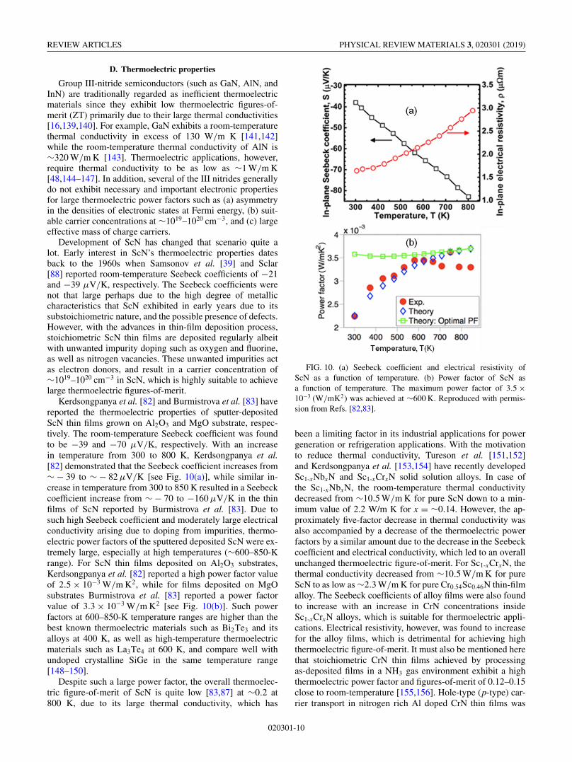
Kerdsongpanya et al. [82] and Burmistrova et al. [83] havereported the thermoelectric properties of sputter-depositedScN thin films grown on Al2O3 and MgO substrate, respec-tively. The room-temperature Seebeck coefficient was foundto be −39 and −70 μV/K, respectively. With an increasein temperature from 300 to 800 K, Kerdsongpanya et al.[82] demonstrated that the Seebeck coefficient increases from∼ − 39 to ∼ − 82 μV/K [see Fig. 10(a)], while similar in-crease in temperature from 300 to 850 K resulted in a Seebeckcoefficient increase from ∼ − 70 to −160 μV/K in the thinfilms of ScN reported by Burmistrova et al. [83]. Due tosuch high Seebeck coefficient and moderately large electricalconductivity arising due to doping from impurities, thermo-electric power factors of the sputtered deposited ScN were ex-tremely large, especially at high temperatures (∼600–850-Krange). For ScN thin films deposited on Al2O3 substrates,Kerdsongpanya et al. [82] reported a high power factor valueof 2.5 × 10⁻³ W/m K2, while for films deposited on MgOsubstrates Burmistrova et al. [83] reported a power factorvalue of 3.3 × 10⁻³ W/m K2 [see Fig. 10(b)]. Such powerfactors at 600–850-K temperature ranges are higher than thebest known thermoelectric materials such as Bi2Te3 and itsalloys at 400 K, as well as high-temperature thermoelectricmaterials such as La3Te4 at 600 K, and compare well withundoped crystalline SiGe in the same temperature range[148–150].
Despite such a large power factor, the overall thermoelec-tric figure-of-merit of ScN is quite low [83,87] at ∼0.2 at800 K, due to its large thermal conductivity, which has
FIG. 10. (a) Seebeck coefficient and electrical resistivity ofScN as a function of temperature. (b) Power factor of ScN asa function of temperature. The maximum power factor of 3.5 ×10⁻³ (W/mK2) was achieved at ∼600 K. Reproduced with permis-sion from Refs. [82,83].
been a limiting factor in its industrial applications for powergeneration or refrigeration applications. With the motivationto reduce thermal conductivity, Tureson et al. [151,152]and Kerdsongpanya et al. [153,154] have recently developedSc1-xNbxN and Sc1-xCrxN solid solution alloys. In case ofthe Sc1-xNbxN, the room-temperature thermal conductivitydecreased from ∼10.5 W/m K for pure ScN down to a min-imum value of 2.2 W/m K for x = ∼0.14. However, the ap-proximately five-factor decrease in thermal conductivity wasalso accompanied by a decrease of the thermoelectric powerfactors by a similar amount due to the decrease in the Seebeckcoefficient and electrical conductivity, which led to an overallunchanged thermoelectric figure-of-merit. For Sc1-xCrxN, thethermal conductivity decreased from ∼10.5 W/m K for pureScN to as low as ∼2.3 W/m K for pure Cr0.54Sc0.46N thin-filmalloy. The Seebeck coefficients of alloy films were also foundto increase with an increase in CrN concentrations insideSc1-xCrxN alloys, which is suitable for thermoelectric appli-cations. Electrical resistivity, however, was found to increasefor the alloy films, which is detrimental for achieving highthermoelectric figure-of-merit. It must also be mentioned herethat stoichiometric CrN thin films achieved by processingas-deposited films in a NH3 gas environment exhibit a highthermoelectric power factor and figures-of-merit of 0.12–0.15close to room-temperature [155,156]. Hole-type (p-type) car-rier transport in nitrogen rich Al doped CrN thin films was
020301-10

REVIEW ARTICLES PHYSICAL REVIEW MATERIALS 3, 020301 (2019)
TABLE III. Mechanical properties including the hardness, Young modulus, Poisson ratio, and bulk modulus of ScN presented withexperimental and theoretical/modeling results.
Young’s Bulk modulusMethod Substrate Hardness (GPa) modulus (GPa) Poisson ratio B (GPa) References
ExperimentalSputtering MgO(001) 12.9–25.7 287–408 182 ± 40 Gall et al. [77]
TiN(001)/ MgO(001) 0.20 ± 0.04 187 Gall et al. [93]MBE Si(111) 270 ± 25 0.188 ± 0.1005 Moram et al. [106]Theoretical/modelingLDA and GGA 24.9 368.8 0.19 197.1 Liu et al. [172]FPLMTO 210.364 Tebboune et al. [173]
356 0.25 220 Meenaatci et al. [171]
also achieved in recent years, marking a significant progressin CrN based materials for thermoelectric applications [157].Therefore, similar to the challenges encountered in most otherthermoelectric materials systems [158–161], the reduction inthermal conductivity must be attained without reducing thepower factor to achieve a higher thermoelectric figure-of-merit. In this regard, incorporation of nanoparticles [162–164], phase separation [165,166], a small amount of heavyelement inclusion [167], and other approaches could be ex-plored.
E. Mechanical properties
Like most other TMNs, the mechanical properties of ScNhave been studied for over three to four decades to utilizeits high hardness and large elastic modulus for tribologyapplications [168–170]. The valence electron density thatdetermines the hardness of materials is the highest for ScNamong group 3 nitrides, and as a result ScN thin films exhibithigh mechanical hardness [171]. Gall et al. reported that (001)ScN thin films deposited on MgO substrates with MBE exhibita hardness of 21.2 GPa, and an elastic modulus of 356 GPa atroom temperature [77]. A bulk modulus of 182 GPa was alsoestimated with previously measured Poisson’s ratio values.Subsequently, Moram et al. [106] reported a Young’s modulusof 270 ± 25 GPa and Poisson’s ratio of 0.188 ± 0.002 on(111) oriented ScN thin films deposited on Si substrates withMBE (see Table III).
Sputtered-deposited ScN (001) films grown on MgO sub-strate demonstrate a room-temperature hardness of 21 GPaand Young’s modulus of 356 GPa, which is consistentwith MBE-deposited ScN [77]. Sputter-deposited cubic-Al0.72Sc0.28N thin-film alloys also exhibited a higher hardnessto ∼32 GPa, and cubic-Ti0.5Al0.36Sc0.14N solid solution alloysexhibited [174] an extraordinarily high hardness of 46 GPa.Though the exact mechanism of such high hardness is notclear, authors speculate that incorporation of ScN inside theTi1-xAlxN matrix improves the crystalline quality, thus leadingto higher hardness values.
F. ScN as an interlayer for GaN growth
For solid-state lighting applications, ScN interlayers havebeen utilized to reduce the threading dislocation densitiesin GaN [53,81], that arise due to a large lattice mismatch
(16%) between the film and the sapphire substrate. Thread-ing dislocations are known to reduce efficiencies of GaNbased lasers and light emitting diodes, act as nonradiativerecombination centers reducing light emission efficiencies,and serve as scattering centers for charge carriers, therebyreducing the mobility of the films [139,175,176]. TypicallyGaN films deposited on sapphire substrates exhibit a threadingdislocation density in excess of 5 × 109 cm−2 [177–179].
The lattice constant (a) of ScN is 4.50 Å, and the a lat-tice parameter for GaN is 3.18 Å which results in −0.1%lattice mismatch for (111) oriented cubic ScN and (0001)oriented hexagonal GaN [145]. Therefore, ScN interlayersshould ideally reduce the threading dislocation density ofGaN epilayers deposited on sapphire substrates. Using thishypothesis, Moram and coworkers [53,81] have demonstratedreduction of threading dislocation density in (0001) GaN from(5.0 ± 0.5) × 109 to (3.1 ± 0.4) × 107 cm−2 for coalescedfilms and to below 5 × 107 cm−2 for partially coalesced films[see Fig. 11(a)]. Microscopic analysis showed that ScN acts asan effective interlayer, and reduces the threading dislocationdensities both for nonpolar (112̄0) and semipolar (112̄2) GaNfilms by orders of magnitude. In addition to reducing thethreading dislocation densities, basal plane stacking faultswere also significantly reduced [81] by the ScN interlayers.
The effect of ScN interlayer thickness on the threadingdislocation density reduction was also studied [54] in coa-lesced GaN films, and results showed [see Fig. 11(b)] thatwith an increase in interlayer thickness from 2 to 12 nmthe threading dislocation density reduced from 10.5 × 10⁷
to 4.5 × 107 cm−2. The films do not coalesce easily for aninterlayer thickness of more than 15 nm, thus setting an upperlimit of ScN interlayer thickness.
V. DEFECTS IN ScN: FIRST-PRINCIPLESTHEORY AND EXPERIMENTS
Native defects and foreign impurities play a crucial rolein determining the physical properties of semiconductors[180] and ScN is no exception. Thin-film growth techniques(such as magnetron sputtering, MBE, etc.) usually possess abackground pressure arising from water vapor, O2, CO2,and other impurity gases that usually dope an otherwiseintrinsic semiconductor with point defects such as vacancies,interstitials, antisite defects, etc. [181,182]. Similarly crystal
020301-11

REVIEW ARTICLES PHYSICAL REVIEW MATERIALS 3, 020301 (2019)
FIG. 11. (a) Threading dislocation density of GaN thin film wasreduced by orders of magnitude with a ScN interlayer shown in thisHRTEM micrograph. (b) Dislocation density is plotted as a functionof ScN interlayer thickness, which showed that with an increasein interlayer thickness from 2 to 12 nm the dislocation densityis reduced by a factor of ∼10. Reproduced with permission fromRef. [54].
structure, lattice constant, and surface and interface energymismatch between the substrate and film result in extendeddefects such as dislocations, grain boundaries, stacking faults,etc. [183,184]. In the case of ScN, the effects of point defects(both native and foreign impurities) have been studied in aseries of recent reports [185–187]. However, the nature andeffects of the extended defects still require detailed analysis.In this section, we will address defects in ScN that areinvestigated by a combination of first-principles theory andexperimental analysis.
A. Effect of nitrogen vacancy and other native defects
Nitrogen vacancies are a common point defect in manynitride semiconductors and affect their electronic as well asoptoelectronic properties [138,188]. The presence of nitrogenvacancies was of great concern in the first few reports on ScNgrowth in the 1960s [40,74]. However, HVPE deposited ScNthin films by Dismukes [72] appeared to be relatively freefrom such defects based on three observations: (a) chemicalanalysis showed that HVPE deposited ScN films are stoichio-metric and no gross deviation from the stoichiometry wasobserved for a range of deposited films; (b) no systematicincrease in donor concentration was observed over the rangeof growth temperature 750–1150 ◦C; and (c) the donor con-centration decreased with a decrease in ammonia and hydro-gen halide concentration during the HVPE process. Following
FIG. 12. DFT based calculation of native points defect formationenergy in ScN. Reproduced with permission from Ref. [185].
this early work, XPS analysis by Porte [75] showed that ScNthin films prefer a stoichiometric condition, and growth ofScN in nitrogen deficient conditions results in stoichiometricScN and metallic scandium mixtures, with no signature of anynitrogen deficient substoichiometric ScN. Therefore, their re-sults indicated that nitrogen vacancy perhaps is not a favorabledefect inside ScN.
More recently, Al-Brithen et al. [100] showed that for MBEgrown ScN films stoichiometry is a strong function of theSc/N flux ratio during the deposition process. For scandiumrich conditions, the bulk Sc/N ratio approximately equals theflux ratio during the growth process; however, as the rocksaltstructure of the crystal was maintained, it resulted in nitrogenvacancies. For nitrogen rich conditions, nitrogen vacancieswere suppressed and the films were stoichiometric. Similarly,Oshima et al. [102] obtained stoichiometric ScN thin filmswith HVPE growth method, and Kerdsongpanya et al. [82]reported nearly stoichiometric films via magnetron sputtering.
Thermodynamics of nitrogen vacancy formation insideScN have been calculated recently using first-principles DFTmethods by Kumagai et al. [185] and presented in Fig. 12.Results showed that for Sc rich conditions nitrogen vacancyformation energy is negative in the entire range of Fermienergy, which could generate a large number of carriers(electrons). However, at N rich conditions, nitrogen vacancyenergy was found to be positive, and it does not cause aFermi-level pinning inside ScN’s band gap. The thermody-namic analysis, therefore, is consistent with the experimentalobservations of MBE deposited ScN thin films by Al-Brithenet al. [100]. Calculation by Kumagai et al. [185] also showedthat p-type doping in ScN is thermodynamically attainableas long as carrier compensation by unintentional impuritiesis well suppressed and a suitable hole dopant is chosen (seeFig. 13).
The nitrogen vacancy defect states are composed mainlyof Sc eg orbitals. Interestingly, the calculations revealedthat only VN
2+ emerges inside the band gap, which is notstable compared to the 1+ and 3+ charge states in traditionalIII-nitride semiconductors [189–191]. When the localized dorbitals constitute mainly the defect state, as with VN in ScN,the on-site Coulomb repulsion is expected to be large. Asa result, VN preferentially accommodates only one electron,which is the reason why VN
2+ is relatively stable in ScN.Electronic structure calculations [186] showed that nitrogenvacancies introduce an asymmetric peak close to the Fermilevel in ScN, and the Fermi energy shifts from the band gap tothe conduction-band edge.
020301-12

REVIEW ARTICLES PHYSICAL REVIEW MATERIALS 3, 020301 (2019)
FIG. 13. Formation energy of n-type and p-type dopants insideScN calculated by DFT based analysis. Mg incorporation energyin Sc atomic sites was found to be favorable, suggesting that p-type doping of ScN is possible. Reproduced with permission fromRef. [185].
Apart from nitrogen vacancy, the formation energies ofother native point defects such as nitrogen or scandium inter-stitials, scandium vacancy, etc., were found to be quite large(see Fig. 12). Similarly antisite defect formation energies arealso very high. Therefore, their effects could be neglected to alarge extent.
B. Effect of oxygen impurity
Oxygen impurities in ScN originate primarily from sourcecontaminations and background H2O, O2, and CO2 gas con-centrations during the thin-film deposition. Mass spectro-scopic analysis of ScN thin films deposited with HVPEmethod [72] exhibited an O2-impurity concentration of 4 ×10¹⁹ atoms/cm−3. More recently, sputter-deposited ScN thinfilm [83] also exhibited 1.6 ± 1.0 at. % of oxygen, and forScN films deposited on Al2O3 substrates [85] the oxygen-impurity content was lower at 0.3 at. %. Moram et al. [192]have showed that compared to other TMNs such as TiN,ZrN, etc., ScN is unusually susceptible to O2 contaminations.Therefore, an in-depth understanding of the thermodynamicsof oxygen-impurity formations inside ScN and its effects onthe physical properties is necessary.
First-principles DFT [185] calculations have showed thatthe formation energies of oxygen impurity on the nitrogenatomic site (ON) are energetically favorable across the wholerange of Fermi energy (see Fig. 14). Oxygen impurities shouldalso act as single donors. Therefore, experimentally observedoxygen impurities in HVPE or sputter-deposited ScN thinfilms are well explained by the thermodynamic analysis. Withsystematic variations of such impurity concentration in ScN,Burmistrova et al. [83] have showed that (a) the O2-defectstates do not reside inside the band gap of ScN, (b) there isno tendency of oxygen atoms to cluster and form precipitates,and (c) the presence of O2 in ScN shifts the Fermi energyfrom ScN’s band gap to its conduction-band edge. Such Moss-Burstein shift of the Fermi level was explained by the donornature of oxygen impurities. Calculations have showed thatfor 1.56 at. % of O2 inside ScN the Fermi level should belocated at ∼0.34 eV from the conduction-band edge.
FIG. 14. DFT analysis of foreign impurity points defect forma-tion energy in ScN. Results show that for oxygen, fluorine, andhydrogen impurities at nitrogen atomic sites the formation energiesare negative, suggesting their possible presence in ScN films. Repro-duced with permission from Ref. [185].
Moss-Burstein shift of the Fermi level to the conduction-band edge has enormous consequences on ScN’s electronicproperties. Measurements have showed that the electrical re-sistivity of ScN epilayers increases from 0.3 m� cm at 300 Kto ∼0.9 m� cm at 800 K [87], which represents its degener-ate semiconducting or semimetallic transport behavior. Suchtransport characteristics can be well explained with the Moss-Burstein shift of the Fermi level. Similarly, the origins of highSeebeck coefficients and large thermoelectric power factors insputter-deposited ScN thin film are also well explained by theFermi-level position at the conduction-band edge. Boltzmanntransport equation based modeling of Seebeck coefficients hasshowed that the experimental Seebeck coefficients could bewell described for a Fermi-level position that is 0.06–0.09eV above the conduction-band edge, which matches well withDFT calculations.
Moram et al. [192] also studied the effects of oxygenincorporation in ScN’s optical and electronic properties byaltering the deposition conditions and background pressureof ScN growth. Results showed that with an increase inthe O2 concentration direct band gap increased from 2.2 to∼3.1 eV, similar to the case of fluorine doped ScN [121],while the crystal structure degraded progressively with theincorporation of O2. Oxygen contaminations also contributedto the non-Arrhenius behavior of ScN film’s resistivity versustemperature behavior, and ultimately resulted in its degeneraten-type conductivity.
C. Effect of foreign impurities
Apart from the presence of native defects and oxygenimpurities, several other foreign impurities such as fluorine[F], hydrogen [H], carbon [C], silicon [Si], tantalum [Ta],etc., have been observed in ScN films. Many of these foreignimpurities arise from thin-film deposition processes relatedto reactant gas, metal precursors, sputtering targets, etc. Forexample, HVPE deposited ScN thin films in the early 1970s[72] contained 3 × 1019 cm−3 metal atom impurities arisingmainly from [Si], [Fe], [Al], [Mg], and other rare-earth metals.Halogen impurities (such as chlorine [Cl] and others) werealso found in HVPE deposited films arising from reactants.However, as mentioned before, in a recent report of HVPE de-posited ScN [102], most of the metal impurity concentrationswere effectively suppressed with a corrosion resistant reactionchamber.
020301-13

REVIEW ARTICLES PHYSICAL REVIEW MATERIALS 3, 020301 (2019)
For sputter-deposited ScN thin films, apart from O2 con-tamination, the presence of [Ta] and [F] has been widelyreported to arise potentially from sputtering targets. In thecase of [F], processing of bulk ore used for target prepara-tion, when the ore is etched by fluorine-containing acids toform an intermediate scandium fluoride step before obtainingscandium metal, introduces the impurities. Deng et al. [121]reported a [Ta] concentration of 0.04 ± 0.01 at. % in ScN,which was also observed in sputter-deposited ScN thin films[114]. [Ta] concentration remained relatively unchanged withrespect to the changes in Ta-target lifetime. However, [F]concentration decreases from 3 ± 1 to <0.5 at. % over thesputter target lifetime.
The thermodynamics and defect formation energies ofseveral of these foreign impurities have been calculated byKumagai et al. [185]. Results showed that the formationenergies of both the FN and HN impurities are negative forthe whole range of Fermi-level position in Sc rich depositionconditions (see Fig. 14). FN was found to be a double donor,consistent with recent observations that FN doping introducescarrier electrons up to 1.3 × 1021 cm−3 in sputter-depositedScN. Similarly, HN impurities form a multicenter bondingwith six Sc neighbors and act as a double donor, whichis found in some other III-nitride semiconductors as well.At nitrogen rich conditions, HN preferentially locates at theinterstitial site near nitrogen with the N-H bond distance of1.03 Å.
VI. COMPENSATION OF NATIVE DONOR DOPINGIN ScN: p-TYPE Sc1-xMgxN
Preferential doping of semiconductors with electron (n-type) and hole (p-type) carriers is one of the most funda-mental requirements for its applications in solid-state de-vices such as pn junctions [193–195], light emitting diodes[196–198], semiconductor lasers [199,200], thermoelectricdevice modules [180,201], etc. Preferential p-type doping ofwurtzite-nitride semiconductors such as GaN was challeng-ing in the early years of its development. However, Amanoet al. [202] demonstrated Mg doped p-type GaN growth byelectron-beam irradiation, and later research by Nakamuraet al. [203] demonstrated p-type GaN thin-film growth byannealing MOCVD deposited Mg doped GaN thin films in-side N2 and NH3 environments. It is a well-established factnow that the development of p-type GaN was instrumentalin GaN’s eventual rise as perhaps the most famous nitridesemiconductor, and paved the way for the demonstration ofhighly efficient light emitting diodes that transformed oursociety with solid-state lighting [204,205]. Therefore, for ScNto achieve wide scale industrial applications there is no doubtthat preferential and easy to achieve n-type and p-type dopingwould be absolutely necessary.
All initial attempts to develop p-type ScN thin films in the1970s were not successful. Dismukes [72] tried to depositp-type ScN thin films during HVPE growth process by theaddition of C and Si as dopants during the growth process.However, no p-type carrier conversion occurred, nor wasthe high electron concentration reduced. Further efforts toperform postgrowth annealing of ScN thin film at 1000 ◦C
in the atmosphere of p-type dopants such as Zn or Mg or invacuum were also not successful in achieving a p-type ScNfilm. Annealing of ScN in Zn-vapor for 1 h showed no appre-ciable changes on the electrical properties, while annealing inMg-vapor reduced the carrier concentration from 2.3 × 10²⁰
to 1.1 × 1020 cm−3 and significantly increased Hall mobilityfrom 19 to 158 cm2/V s. Annealing in vacuum, on the otherhand, proved to be detrimental with an increase in electronconcentration and reduction in carrier mobility. In no casecould the authors achieve p-type doping in ScN thin film.Even though research in ScN stagnated for the next fewdecades, subsequent growth of ScN thin film with MBE andmagnetron sputtering starting in the 1990s and early 2000salso did not address the p-type doping.
Saha et al. developed p-type ScN thin film by reactivemagnetron cosputtering with the incorporation of MgxNy [33]and MnxNy [86] inside a ScN thin-film matrix. Physicalproperties of p-type Sc1-xMgxN and Sc1-xMnxN films werealso studied with a motivation to develop electronic, opto-electronic, and thermoelectric devices. Results showed thatwith an initial increase in the MgxNy concentration from 0to ∼2.5 at. % room-temperature resistivity of the Sc1-xMgxNfilms increased from ∼0.3 to more than 7 × 10³ m� cm,which amounts to a more than 104-factor increase (seeFig. 15). Such resistivity increase was also associated withdecrease in the electron concentration from ∼6 × 1020 cm−3
for undoped ScN thin film to ∼2 × 1018 cm−3 for x ∼ 0.017.Further increase in MgxNy concentrations inside ScN filmresulted in an electron-to-hole carrier type transition withresistivity decreasing to 2 m� cm with increased MgxNy con-centrations. Decrease in resistivity was associated with an in-crease in hole concentrations to a maximum 2.2 × 1020 cm−3
for p-type Sc1-xMgxN thin-film alloys. Hall mobility wasfound to decrease initially from ∼63 cm2/V s to less than∼5 cm2/V s with an increase in MgxNy content in the n-typecarrier transport regime. However, mobilities recovered to amoderate 10–20 cm2/V s range for samples with high holeconcentrations.
Structural characterization of the Sc1-xMgxN thin filmswith high-resolution XRD and high-resolution transmissionelectron microscopy (HRTEM) also revealed [86] that thealloy films are substitutional solid solutions without anyMgxNy precipitations, phase separations, or secondary phaseformations, and exhibited rocksalt crystal structure with lat-tice constants that are very close to that of undoped ScN.Optical characterization with UV-visible spectroscopy mea-surements showed direct band-gap optical absorption in pureScN and in all n-type and p-type Sc1-xMgxN thin-film alloys.No signature of any sub-band-gap absorption was observed,which demonstrates that MgxNy incorporation inside the ScNmatrix does not add any defect states inside ScN’s directband gap or alter its basic band structure. The role of Mgdoping was to act as an electron acceptor that reduces car-rier concentration of pure ScN and eventually leads to p-type Sc1-xMgxN thin-film alloys. Irrespective of the carriertype, all Sc1-xMgxN thin-film alloys exhibited a direct gapof ∼2.25 eV, which is the same as a direct band gap ofpure ScN and supports the observation that the underly-ing electronic structure of ScN is unchanged after MgxNy
incorporation.
020301-14

REVIEW ARTICLES PHYSICAL REVIEW MATERIALS 3, 020301 (2019)
FIG. 15. (a) Variation of room-temperature resistivity (ρ) and carrier concentration (n or p) as a function of Mg target power and MgxNy
concentration inside the ScN matrix. (b) Variation of room-temperature mobility and Seebeck coefficient (S) as a function of Mg target powerand MgxNy concentration inside the ScN matrix. Reproduced with permission from Ref. [86].
Temperature-dependent resistivity measurements showedthat with an increase in temperature from 300 to 850 K,and similar to the case of undoped ScN (see Fig. 5), p-type Sc0.962Mg0.038N thin film (having the largest hole con-centration) exhibits an increase in resistivity from ∼2.5 to∼6 m� cm amounting to an approximately three-factor in-crease (see Fig. 16). Such increase in resistivity is represen-tative of degenerate semiconducting or semimetallic nature.Subsequent modeling analysis revealed that heavy hole dop-ing pushes the Fermi level inside the valence band of ScN,which gives rise to the increase in resistivity with the increasein temperature. It is similar to the case of undoped ScN, whereunwanted oxygen impurities push the Fermi level from themiddle of the band gap to inside the conduction band. Hallmobility of the films decreased from ∼20 to ∼8 cm2/V scorresponding to the same increase in temperature, and ex-hibited an exponent of −0.71, which is consistent with alloyscattering of holes at higher temperatures. The hole concen-trations remained relatively unchanged with the increase intemperatures.
Temperature-dependent Seebeck coefficients and thermo-electric power factors of both n-type and p-type Sc1-xMgxNthin films have been investigated in detail [87], and resultswere explained with modeling analysis. All n-type and p-type Sc1-xMgxN thin films exhibited high Seebeck coefficientvalues. For p-type Sc0.962Mg0.038N, the Seebeck coefficientincreased from ∼50 μV/K at 300 K to ∼225 μV/K at 850 Kamounting to an approximately four-factor increase. Suchlarge Seebeck coefficients resulted in high thermoelectricpower factors of 7 × 10⁻⁴ to 8 × 10⁻⁴ W/m K2 at 700–850 Kin p-type Sc0.962Mg0.038N thin film. Power factors of otherp-type Sc1-xMgxN thin films were also large due to their highSeebeck coefficients.
Optimized power factors calculated by adjusting the carrierconcentrations in n-type and p-type film showed (presented inFig. 17) that the experimental power factors were close to thetheoretically predicted optimum values, which meant that thecarrier concentrations were already at the optimal level. Mod-eling analyses also revealed that for p-type Sc0.962Mg0.038Nthin film the Fermi level was ∼0.2 eV below the valence-bandmaxima, which is similar to the case for pure-ScN, wherethe Fermi level was found to be 0.06–0.12 eV above the
conduction-band minima at 800 K. A plot of Fermi-levelposition with respect to the doping level in ScN at 800 K (pre-sented in Fig. 17) also shows that the carrier concentrationsfor both n-type and p-type doping need to be reduced to below3 × 1019 to 4 × 1019 cm−3 if the Fermi level is to be pushedinside the band gap.
The effects of p-type dopants on the electronic struc-ture of ScN were also evaluated [186] using first-principlesDFT based calculations. For nitrogen rich conditions MgSc
exhibited a shallow acceptor behavior. Furthermore, MgSc
was found to be lower in energy than VN in the band gap,suggesting that Mg is a good acceptor dopant in ScN. Elec-tronic structure calculations also revealed that for 3.125% Mgdoping the Fermi level moves from the band gap to inside0.4 eV below the valence-band maxima, which is consistentwith experimental observations.
Apart from Sc1-xMgxN, p-type Sc1-xMnxN thin-film alloyswere also developed [33] with the incorporation of MnxNy
inside the ScN matrix. Mn doping was found to exhibitmidgap defect states, and altered the basic band structure ofScN significantly. Moreover, the amount of Mn required toachieve p-type Sc1-xMnxN was also relatively larger in the 5.8to 11% range. Nevertheless, both Mg and Mn doping in ScNproved to be effective for producing p-type ScN thin films,which will undoubtedly further the prospects of ScN basedelectronic and optoelectronic device technologies.
VII. ScN-WURTZITE (III-NITRIDE) ALLOYS
Several ScN-wurtzite (III-nitride) semiconductors [206](such as wurtzite-Al1-xScxN, wurtzite-Ga1-xScxN, rocksalt-Al1-xScxN, etc.) have attracted interest in recent years forapplications in piezoelectric materials [207] for surface andbulk acoustic resonators, micromachined ultrasound transduc-ers [208], epitaxial metal/semiconductor superlattice growth[60,209], etc. In this section, we will discuss the physicalproperties of ScN (III-nitride) solid solution alloys.
A. Wurtzite Al1-xScxN: Piezoelectric materials and devices
As the demands for higher-temperature sensors are in-creasing drastically for applications in automobiles, aircrafts,
020301-15

REVIEW ARTICLES PHYSICAL REVIEW MATERIALS 3, 020301 (2019)
FIG. 16. Temperature-dependent (a) electrical resistivity, (b) mobility, and (c) carrier concentration of p-type Sc0.962Mg0.038N alloy films.Reproduced with permission from Ref. [86].
turbine engines, monitoring of furnaces, turbine systems,etc., piezoelectric materials have become increasingly attrac-tive and important [210–212]. It is a well-established phe-nomenon that materials with higher piezoelectric coefficientspossess lower Curie temperatures [65,213]. For example, theCurie temperature and piezoelectric coefficient d33 of leadzirconium titanate (PZT), which is widely used in manyelectronic devices, are 250 ◦C and 410 pC N−1, respectively[214]. Similarly, AlN exhibits a Curie temperature of 1150 ◦C,but with significantly lower piezoelectric coefficient d33 of5.5 pC N−1 [215]. Therefore, designing materials that exhibitboth higher Curie temperature and larger piezoelectric re-sponse will greatly improve many piezoelectric devices suchas acoustic resonators, sensors, etc.
Among the III-nitride semiconductors, AlN exhibits themaximum piezoelectric coefficient and has already at-tracted significant interest for applications in micro-electro-mechanical (MEMS) devices. Akiyama et al. [65,213] demon-strated (see Fig. 18) that the piezoelectric coefficients of AlNcan be increased by more than 400% with the incorporationof ScN inside the AlN matrix. The piezoelectric coefficientd33 of Al1-xScxN alloy film was measured to be 27.6 pC N−1,which is the highest among the reported tetrahedral bonded
FIG. 17. Optimized (a) thermoelectric power factor and (b)Fermi energy plotted as a function of the n-type and p-type carrierconcentrations inside ScN at 800 K. The Fermi energy positionsare referenced with respect to the conduction- and valence-bandedges. The figure shows that power factor values at high temperatures(800 K) are already optimized with respect to the carrier concentra-tion in the n-type and p-type films. Reproduced with permission fromRef. [87].
semiconductors. Moreover, the piezoelectric coefficients re-mained unchanged even after annealing the alloy at 550 ◦Cfor more than two days in vacuum. Piezoelectric propertiesof sputtered-deposited Al1-xScxN thin films were also mea-sured as a function of scandium nitride concentrations, whichshowed that the hexagonal intermediate phase of Al1-xScxNalloys demonstrates the largest piezoelectric response.
The origin of such large enhancement in the piezoelectricresponse was investigated with first-principles DFT basedcalculations [63,207,216–219], which showed that the in-crease is an intrinsic alloying effect. Alloying was found toinfluence the energy surface topology, which leads to largeelastic softening along the crystal parameter c and raisessignificantly the intrinsic sensitivity to axial strain that re-sulted in the enhanced piezoelectric coefficients. Modeling
FIG. 18. Influence of Sc concentration on crystal growth ofScxAl1-xN alloys at Sc concentrations of (a) 41%, (b) 42%, (c)43%, and (d) 45%. For Sc concentration below 41%, the structureis hexagonal, above 46% the structure is cubic, and between 42 and45% both the cubic and hexagonal structure are present. (e) Variationof piezoelectric response d33 as a function of Sc concentration,showing maximum response at 43% Sc concentration. Reproducedwith permission from Ref. [65].
020301-16

REVIEW ARTICLES PHYSICAL REVIEW MATERIALS 3, 020301 (2019)
also revealed that the flattening of the energy landscape wasa consequence of the competition between the parent wurtziteand the so far experimentally undiscovered hexagonal phaseof the Al1-xScxN alloy that was responsible for this largeenhancement in piezoelectricity.
Al1-xScxN alloy based surface acoustic wave (SAW) de-vices with enhanced performance have also been demon-strated recently, highlighting their potential applications inMEMS based energy harvesting devices [26,67,220,221].Compared to an AlN based SAW device, the Al1-xScxNalloy devices exhibited much better transmission properties[222,223]. The electromechanical coupling coefficient K2 wasalso found to be in the range between 2.0 and 2.2% fora wide normalized thickness range, which is a more than300% increase when compared to that of an AlN based SAWdevice. Similarly, acoustic delay lines based on piezoelectricAl1-xScxN thin-film hybrid transducers are also investigated[224] with modeling analyses. Results showed that such anovel hybrid resonator in which a bulk acoustic wave trans-forms into a SAW due to the special pillars patterned on thepiezoelectric Al1-xScxN thin film should be promising dueto the high electromechanical coupling of greater than 4%[208,225].
B. Wurtzite Ga1-xScxN
Ga1-xScxN alloy films have been developed [226,227]by the solid-state alloying between GaN and ScN mainlyby MBE method, and exhibited different crystal structuresdepending on the ScN concentration inside the Ga1-xScxNmatrix [228–230]. Dismukes and Moustakas [231] showedthat GaN and ScN should be highly soluble in one anotherin the rocksalt crystal structured Ga1-xScxN phase, and thewurtzite crystal phase was stable for up to an intermediateScN concentration. Calculations [229,232] also suggested aprecise phase transition point at x = 0.26 for Ga1-xScxN be-yond which the alloy undergoes a wurtzite-to-rocksalt struc-tural phase transition.
Little and Kordesch [233] used reactive magnetron sputter-ing to deposit Ga1-xScxN alloy thin films on quartz substrates.XRD analysis revealed that the films exhibit amorphous andpolycrystalline structure for 0.2 < x < 0.7, and the directband gap was found to decrease linearly from 3.5 to 2 eVwith an increase in the ScN concentrations. Radio-frequencyplasma nitrogen source MBE deposited films under nitrogenrich conditions revealed three crystal phases—(a) wurtzite-like (x < 0.17), (b) transitional (0.17 < x < 0.54), and (c)
rocksalt (x > 0.54)—in Ga1-xScxN thin films and a lineardecrease in band gap with increasing ScN concentrations con-sistent with the observations by Little et al. (see [234]). MBEdeposited Ga1-xScxN thin-film alloys by Knoll et al. [230,235]contained high densities of a-type threading dislocations bentat the interfaces, which relax the misfit strains (see Fig. 19).All deposited films (having x = 0.08) were also found tobe unintentionally n doped and PL measurements showedthat they emit at 362 nm. Dislocation densities were foundto be comparable to the GaN template and a significantlyhigher density of I1-type basal plane stacking faults and planardefects were observed in the film with x = 0.06 [235,236].
Valence-band offsets between Ga1-xScxN/AlN andGa1-xScxN/GaN heterojunctions were also measured withXPS based analysis [237,238]. Results showed that thevalence-band offset for Ga1-xScxN/AlN heterojunctionsincreased from 0.42 to 0.95 eV with an increase in the Scconcentration from 0 to 1.5%. Such increases in the bandoffsets were due to the internal distortions in bonding thatresult from the introduction of ScN into the GaN matrix[238]. The type-I band alignments in Ga1-xScxN/AlN aresuitable for UV optoelectronic applications [239,240]. On theother hand, type-II alignment was determined between theGa1-xScxN/GaN interfaces, which could expand the range ofits applications [234,241–243].
C. Rocksalt Al1-xScxN
Unlike its wurtzite counterpart, rocksalt-Al1-xScxN hasattracted little attention [244,245]. Early reports [244,246]have showed that magnetron sputtered Al1-xScxN alloy filmsdeposited on sapphire and MgO substrates stabilize in rocksaltstructure for maximum AlN mole fractions up to 60%. Furtherincrease in AlN mole fractions leads to phase separation ofAl1-xScxN into rocksalt and wurtzite structures, before even-tually converting the alloys into complete wurtzite structuredgrains [245,247,248]. Postgrowth annealing of Al0.43Sc0.57Nthin film at 1000–1100 ◦C also resulted in phase separationsinto nonisostructural cubic-ScN and wurtzite-structured AlNphase via nucleation and growth at grain boundaries due tovolume mismatches. With an increase in AlN mole fractionfrom 0 to 50%, the lattice constants of the rocksalt-Al1-xScxNalloy were found to decrease from 4.52 to 4.30 Å (see Fig. 20),which matches well with theoretical calculations. Such adecrease in lattice parameters is not surprising given that thestable rocksalt ScN exhibit a lattice constant of 4.52 Å, whilerocksalt-AlN, though it is not stable at ambient conditions
FIG. 19. Cross-sectional weak-beam dark field TEM images of ScxGa1-xN (x = 0.08) on the GaN template revealing c, (a+c) threadingdislocations (0002) and a, (a+c) threading dislocations. Reproduced with permission from Ref. [226].
020301-17

REVIEW ARTICLES PHYSICAL REVIEW MATERIALS 3, 020301 (2019)
FIG. 20. Direct band gap of the rocksalt-AlxSc1-xN alloys pre-sented as a function of their lattice constants. Lattice parametersof the rocksalt metallic nitrides are also plotted in the same figure,which show that the rocksalt-AlxSc1-xN can be lattice matched withmost other metallic TMN for superlattice growth. Reproduced withpermission from Ref. [60].
and can only be stabilized at high pressures, exhibits a latticeparameter of 4.08 Å [249–251].
The maximum AlN mole fraction required to stabilizeAl1-xScxN alloys in rocksalt phase was further increased from60% to ∼84% with epitaxial stabilization technique by de-positing a thin 20-nm TiN seed layer on (001) MgO substrates[60]. Reduced lattice mismatch at TiN/rocksalt-Al1-xScxNinterfaces and decreased bond polarity mismatches resultedin metastable rocksalt Al1-xScxN alloy films with 0.62 < x <
0.82. HRTEM imaging showed that rocksalt-Al0.72Sc0.28Nalloys grow with a cube-on-cube epitaxial relationship onTiN/MgO substrates without any signature of misfit dislo-cations. Critical thickness for stabilizing the rocksalt phasewas found to exceed more than 120 nm for an Al0.72Sc0.28Nthin film deposited on 20-nm TiN/MgO substrate. At an AlNmole fraction of more than ∼84%, Al1-xScxN thin films, how-ever, undergo metastable-rocksalt to stable-wurtzite structuralphase transition.
Microstructural evolution and epitaxial relationships dur-ing such metastable-rocksalt to stable-wurtzite structuralphase transformation were also determined with HRTEManalysis [252]. An Al1-xScxN alloy film was deposited onTiN/MgO substrates at a composition chosen to be at thephase boundary between the rocksalt and wurtzite phases,and a thin-film snapshot of the transformation was capturedwith HRTEM. Microstructural information revealed that thetransformation was triggered by defects at the rs-{01̄1} growthfront that offer a nearly invariant plane with respect to theparallel w-{21̄1̄0} planes. Pyramidal rocksalt-Al1-xScxN re-gions surrounded by the wurtzite-Al1-xScxN matrix with twin-ing relationships were also found. As most other III-nitridesemiconductors exhibit a wurtzite-to-rocksalt structural phasetransition upon applications of hydrostatic pressure inside di-amond anvil cells, where a detailed microscopy analysis is notalways feasible, the epitaxial and microstructural informationobtained with Al1-xScxN thin-film alloys is expected to carryover to such systems.
In terms of the electronic properties, with an increase inAlN content, resistivity of the Al1-xScxN alloy films increased
by more than two orders of magnitude within the rocksaltphase. A sharp decrease in the Hall mobility and appreciablechanges in the carrier concentrations were also observed.However, as the alloys undergo the rocksalt-to-wurtzite struc-tural phase transitions, the resistivity of the wurtzite filmsincreased by six to ten orders of magnitude with an associatedorder-of-magnitude decrease in carrier concentrations. Simi-larly, optical properties such as direct band gap and dielectricpermittivity of Al1-xScxN alloy films were also evaluated [60].The direct band gap was found to increase with increasein AlN mole fractions from 2.2 eV to ∼4 eV within therocksalt crystal structure composition range, and exhibiteda moderate band-gap bowing with a bowing parameter of1.4 ± 0.19 eV, which is close to other III-nitride alloys suchas (Al, Ga)N, (In, Ga)N, etc. Interpolation of the results alsoshowed that rocksalt-AlN would exhibit a direct band gapof 4.70 ± 0.20 eV, which is close to the theoretical predic-tion of 4.99 eV. Spectroscopic ellipsometer measurementsrevealed that the dielectric permittivity of the Al1-xScxN alloysdecreases with an increase in the AlN mole fractions asexpected.
VIII. METAL/SEMICONDUCTOR HETEROEPITAXY:(Zr,Hf)N/ScN MULTILAYERS AND TiN/(Al,Sc)N
SUPERLATTICES
Defect-free and lattice-matched single-crystalline superlat-tice growth requires that the component materials (metallicand semiconducting layers) should exhibit several criteriasuch as (a) similarity in the crystal structure, (b) closelymatched lattice constants, (c) low surface and interface energydensity, etc. [253]. TMNs are composed of several metallicnitrides [27] (such as TiN, ZrN, HfN, VN, etc.) that exhibitrocksalt crystal structure with lattice constants varying from4.05 to 4.60 Å (see Fig. 20). Therefore, the development ofrocksalt-Al1-xScxN with lattice constants ranging from 4.15 to4.52 Å paves a way to lattice-match most of the TMN metalswith rocksalt-Al1-xScxN (see Fig. 20). For example, ScN (a =4.52 Å is lattice-matched to metallic HfN (a = 4.52 Å and hasa very small mismatch with ZrN (a = 4.59 Å).
Epitaxial lattice-matched ZrN/ScN and HfN/ScNmetal/semiconductor multilayers were deposited on(001) MgO substrates by reactive magnetron sputtering[61,84,254,255]. XRD analysis revealed that the multilayerfilms grow with (002) orientations, and exhibit c-axis latticeconstants of 4.52 and 4.55 Å, respectively, which is anaverage of the individual layer’s lattice parameters [61].XRD also showed the presence of interference fringessuggestive of layer-by-layer epitaxial crystal growth withatomically sharp interfaces. Close inspection of the multilayerstructures with HRTEM, however, revealed that ∼6% latticemismatch between the nitrides and the MgO (a = 4.21 Åsubstrate results in threading dislocations that originate atthe HfN/MgO interface and propagate through the films tothe multilayer surfaces [84,256] (shown in Fig. 21). Due tothe presence of such high densities of threading dislocations(1011 cm−2) reproducible electrical measurements along thecross-plane directions were difficult to achieve.
Development of rocksalt-Al1-xScxN alloy films has suc-cessfully addressed the lattice-mismatch issue and the
020301-18

REVIEW ARTICLES PHYSICAL REVIEW MATERIALS 3, 020301 (2019)
FIG. 21. (a) XRD spectrum of the HfN/ScN multilayer showing002-oriented film growth. (b) HRTEM micrograph of the HfN/ScNmultilayer showing threading dislocations that originate at the mul-tilayer/MgO interface and propagate through the multilayers to thesurface. (c) The inset from (b) shows that along the defect linesindividual layers curve towards the MgO substrate. Reproduced withpermission from Ref. [84].
associated effects of threading dislocations. Rocksalt-Al1-xScxN with x = 0.72 exhibits a lattice constant a =4.25 Å, which is very close to the lattice parameter of one ofthe most famous TMNs, TiN (a = 4.24 Å). At the same time,MgO substrate exhibits rocksalt structure and a lattice con-stant a = 4.21 Å, which is very close to the lattice parametersof the nitrides.
Epitaxial lattice-matched TiN/Al0.72Sc0.28N metal/semiconductor superlattice heterostructures were depositedon (001) MgO substrates by UHV magnetron sputtering[59,60,257]. XRD analysis showed (see Fig. 22) that thefilms grow with (002) orientations with a very small (0.05◦)FWHM of the rocking curve suggestive of a small degree ofmosaicity. RSM exhibited that the asymmetric (024) peaksof the superlattice and MgO are all aligned vertically, whichmeans that along the in-plane directions lattice constants ofthe substrate, TiN, and Al0.72Sc0.28N are all fixed at 4.21 Å,while along the cross-plane directions only a slight relaxationwas observed with TiN exhibiting a c-axis lattice constantof 4.23 Å and Al0.72Sc0.28N alloys exhibiting a c-axis latticeconstant of 4.25 Å. HRTEM imaging showed cube-on-cubeepitaxial crystal growth with sharp and abrupt interfaces.Detailed characterization about thermal, optical, mechanical,and electronic properties of the superlattices was also
performed [174,209,258], which highlighted the potentialand suitability of such novel metamaterials in solid-stateenergy transport and conversion research fields such as inplasmonics [259–261], thermoelectricity [262–265], etc.However, a detailed discussion of the physical properties ofthe superlattices is beyond the scope of this research updateand can be found in Ref. [266].
IX. CONCLUSION AND FUTURE PERSPECTIVE
In conclusion, scandium nitride (ScN) is an emergingrocksalt group 3-nitride semiconductor and shows promise forthe next generation thermoelectric, electronic, and optoelec-tronic device technologies. Rocksalt (cubic) crystal structure,indirect band gap, and ability to preferentially dope ScNwith n-type and p-type carriers will enable several electronicand optoelectronic devices with improved efficiencies. At thesame time, successful demonstration of ScN based epitax-ial metal/semiconductor heterostructure and superlattices isexpected to innovate new physics concepts and device tech-nologies. Though several challenges related to materials anddevices remain to be addressed, here we will discuss a smallnumber of opportunities in ScN research that would bene-fit development of ScN based practical device applications,including applications where ScN is expected to outperformother semiconducting materials.
A. Metallic nanoparticle inclusion in ScN for thermoelectricand terahertz applications
Epitaxial metallic nanoparticles embedded inside a semi-conducting host demonstrate a range of interesting properties.For example, the presence of (semi) metallic nanoparticlescan donate carriers, pin the Fermi level, shorten electron-holerecombination rates, enhance electron tunneling, and increasescattering of phonons in semiconductor host layers, whichleads to efficient thermoelectric, plasmonic, and terahertzoptoelectronic devices. Metallic nanoparticle inclusion insideScN could improve its thermoelectric properties, as well asenable ScN based terahertz sources, detectors, and modula-tors. Heavy metal inclusion (such as W, Mo, or Hf) inside ScNwould presumably reduce its thermal conductivity. Suitablemetallic nanoparticles may also act as a Schottky barrierinside ScN that filters out low-energy electrons to increasethe Seebeck coefficient, and hence improve its thermoelectricfigure-of-merit. Similarly, metallic nanoparticle inclusion in-side ScN (similar to the rare-earth semimetallic ErAs incorpo-ration inside GaAs based III-arsenide semiconductors) couldalso result in photoconductive switches, detectors, etc., for ter-ahertz optoelectronics with tunable spectral ranges [267,268].
B. ScN electronic devices
As ScN exhibited degenerate semiconducting or (semi)metallic characteristics with high carrier concentrations(∼1020–1021 cm−3 at room temperature) for several decades,not much progress has been made in developing ScN basedelectronic devices such as diodes, transistors, etc. However,with the recent progress in hole doping that reduces carrierconcentration, and development of p-type ScN thin film, itshould be possible to develop basic electronic devices such
020301-19

REVIEW ARTICLES PHYSICAL REVIEW MATERIALS 3, 020301 (2019)
FIG. 22. XRD spectra of a 20-nm/20-nm TiN/Al0.72Sc0.28N superlattice that exhibits 002-oriented growth. Superlattice satellite peaks areclearly observed indicating sharp interfaces. (b) Reciprocal space XRD map of the superlattice. Reproduced with permission from Ref. [257].
as pn junctions, Schottky barriers, and transistor devices withScN as the semiconducting material. Since ScN exhibits anindirect band gap of ∼0.9 eV and dielectric permittivity of12.3, which is similar to Si, it may be possible that ScN basedelectronic devices find some applications in industries.
C. Refractory electronics and plasmonics with ScN
Refractory materials [269] in materials science refer tothose materials that exhibit (a) high melting temperatures(>2000 ◦C), (b) stability at high operating temperatures, re-taining their physical and chemical properties, and (c) stableand preferential good contacts with other high-temperaturematerials. Such materials are useful in many industrial ap-plications such as in combustion systems, well logging, in-dustrial processes, supersonic aircrafts, and dense electronicpackaging industries. A good refractory semiconducting ma-terial must exhibit several criteria, such as (a) large bandgap, (b) ease of doping preferentially with p-type and n-typecarriers, (c) large breakdown voltage, (d) ease of fabrication,as well as (e) preferential and stable Ohmic and Schottkycontacts with other metals at high temperatures [270]. Dueto such stringent requirements only a few semiconductors likediamond, SiC, and GaN are traditionally used as refractorysemiconductors.
ScN exhibits a high melting temperature in excess of∼2600 ◦C, and a direct band gap of 2.2 eV, and can bepreferentially doped with both n-type and p-type carriers.
Moreover, metal/ScN epitaxial contacts have also been de-veloped (discussed earlier) that are stable at high operatingconditions. Therefore, ScN and its heterostructures could beexplored for high-temperature electronic applications. How-ever, the band gap of ScN is not as large as that of theother well-known high-temperature materials and this mightlimit its applications to medium-temperature ranges. At thesame time oxidation of ScN at high temperatures could bechallenging. Therefore, much research effort will be neededto explore ScN’s refractory applications, and effective coatingmaterials and processing methods needs to be developed.
Integration of ScN with other transition-metal nitrides likeTiN, ZrN, etc., may also lead to refractory plasmonic het-erostructure devices for harvesting solar energy in solar photo-voltaic and solar thermophotovoltaic devices [271–273]. Forexample, TiN is a promising alternative plasmonic materialfor Au in the visible spectral range, and TiN/Al0.72Sc0.28Nmetal/semiconductor superlattices have demonstrated hyper-bolic metamaterial properties. Their high-temperature prop-erties could be investigated, which may result in promis-ing refractory plasmonic devices with ScN as a componentmaterial.
ACKNOWLEDGMENT
The authors acknowledge financial support from Inter-national Centre for Materials Science in Jawaharlal NehruCentre for Advanced Scientific Research.
[1] R. R. Schaller, IEEE Spectr. 34, 52 (1997).[2] Mark S. Lundstrom, Science 299, 210 (2003).[3] T. S. Cheung and J. R. Long, IEEE J. Solid-State Circuits 41,
1183 (2006).[4] J. R. Long and M. A. Copeland, IEEE J. Solid-State Circuits
32, 357 (1997).[5] J. C. Suhling and R. C. Jaeger, IEEE Sens. J. 1, 14 (2001).[6] D. Hartman, M. Grace, and C. Ryan, J. Lightwave Technol. 3,
729 (1985).[7] H. Iwai and S. Ohmi, Microelectronics Reliability 42, 465
(2002).
[8] M. H. R. Lankhorst, B. W. S. M. M. Ketelaars, and R. A. M.Wolters, Nat. Mater. 4, 347 (2005).
[9] R. J. Gutmann, IEEE Trans. Microw. Theory Tech. 47, 667(1999).
[10] T. D. Moustakas, T. Xu, C. Thomidis, A. Y. Nikiforov, L.Zhou, and D. J. Smith, Phys. Status Solidi Appl. Mater. Sci.205, 2560 (2008).
[11] Y. Huang, X. Duan, YI. Cui, and C. M. Lieber, Nano Lett. 2,101 (2002).
[12] S. Nakamura, T. Mukai, and M. Senoh, Appl. Phys. Lett. 64,1687 (1994).
020301-20

REVIEW ARTICLES PHYSICAL REVIEW MATERIALS 3, 020301 (2019)
[13] N. Shibata, Phys. Status Solidi A 192, 254 (2002).[14] H. J. Joyce, Q. Gao, H. H. Tan, C. Jagadish, and Y. Kim,
Prog. Quantum Electron. 35, 23 (2011).[15] R. F. Davis, Proc. IEEE 79, 702 (1991).[16] S. Strite and H. Morkoç, J. Vac. Sci. Technol. B 10, 1237
(1992).[17] A. J. Turberfield, S. R. Haynes, P. A. Wright, R. A. Ford, R. G.
Clark, J. F. Ryan, J. J. Harris, and C. T. Foxon, Phys. Rev. Lett.65, 637 (1990).
[18] S. Nakamura, M. Senoh, S. Nagahama, N. Iwasa, T. Yamada,T. Matsushita, H. Kiyoku, and Y. Sugimoto, Jpn. J. Appl. Phys.35, L74 (1996).
[19] S. Nakamura, M. Senoh, S. I. Nagahama, N. Iwasa, T. Ya-mada, T. Matsushita, H. Kiyoku, Y. Sugimoto, T. Kozaki, H.Umemoto, M. Sano, and K. Chocho, Appl. Phys. Lett. 72, 211(1998).
[20] D. L. Huffaker, G. Park, Z. Zou, O. B. Shchekin, and D. G.Deppe, Appl. Phys. Lett. 73, 2564 (1998).
[21] J. Han, M. H. Crawford, R. J. Shul, J. J. Figiel, M. Banas, L.Zhang, Y. K. Song, H. Zhou, and A. V. Nurmikko, Appl. Phys.Lett. 73, 1688 (1998).
[22] H. Page, C. Becker, A. Robertson, G. Glastre, V. Ortiz, and C.Sirtori, Appl. Phys. Lett. 78, 3529 (2001).
[23] F. Qian, Y. Li, S. Gradec, and C. M. Lieber, Nano Lett. 4, 1975(2004).
[24] H. Kosaka, A. A. Kiselev, F. A. Baron, K. W. Kim, and E.Yablonovitch, Electron. Lett. 37, 464 (2001).
[25] D. D. Awschalom, D. Loss, and N. Samarth, Semiconduc-tor Spintronics and Quantum Computation (Springer, Berlin,2002).
[26] P. Eklund, S. Kerdsongpanya, and B. Alling, J. Mater. Chem.C 4, 3905 (2016).
[27] L. Toth (ed.), Transition Metal Carbides and Nitrides (Aca-demic, New York, 1971).
[28] N. Takeuchi, Phys. Rev. B 65, 045204 (2002).[29] H. Shimizu, M. Shirai, and N. Suzuki, J. Phys. Soc. Jpn. 66,
3147 (1997).[30] W. Feng, S. Cui, H. Hu, G. Zhang, Z. Lv, and Z. Gong, Physica
B 405, 2599 (2010).[31] B. Saha, J. Acharya, T. D. Sands, and U. V. Waghmare, J. Appl.
Phys. 107, 033715 (2010).[32] A. Qteish, P. Rinke, M. Scheffler, and J. Neugebauer, Phys.
Rev. B 74, 245208 (2006).[33] B. Saha, G. Naik, V. P. Drachev, A. Boltasseva, E. E.
Marinero, and T. D. Sands, J. Appl. Phys. 114, 063519(2013).
[34] C. Stampfl, W. Mannstadt, R. Asahi, and A. J. Freeman, Phys.Rev. B 63, 155106 (2001).
[35] W. R. L. Lambrecht, Phys. Rev. B 62,13538 (2000).[36] X. Bai and M. E. Kordesch, Appl. Surf. Sci. 175-176, 499
(2001).[37] W. Meissner and H. Franz, Z. Phys. 65, 30 (1930).[38] D. Geiselman, J. Less Common Met. 4, 362 (1962).[39] G. V. Samsonov, M. D. Lyutaya, and V. S. Netspor, Zh.
Prikl. Khim. 36, 2108 (1963) [Russ. J. Appl. Chem. 36, 2043(1963)].
[40] M. D. Lyutaya and V. F. Bukhanevich, Zhur. Neorg. Khim. 7,2487 (1962) [Russ. J. Inorg. Chem. 7, 1290 (1962)].
[41] R. F. Voitovich and N. P. Shakhanova, Porosh. Met. 3, 75(1967) [Sov. Pwdr. Met. Metal Cer. 6, 225 (1967)].
[42] L. Kaufman, Trans. AIME 224, 1006 (1962).[43] B. Saha, T. D. Sands, and U. V Waghmare, J. Phys.: Condens.
Matter 24, 415303 (2012).[44] L. Khajavizadeh, Growth and structural characterization of
ScN/CrN periodic and quasi-periodic superlattices for thermo-electric application, Master thesis, Linköping University, TheInstitute of Technology, 2014.
[45] J. L. Schroeder, D. A. Ewoldt, R. Amatya, R. J. Ram, A.Shakouri, and T. D. Sands, J. Microelectromechanical Syst.23, 672 (2014).
[46] A. Shakouri, Annu. Rev. Mater. Res. 41, 399 (2011).[47] J. M. Zide, D. O. Klenov, S. Stemmer, A. C. Gossard, G. Zeng,
J. E. Bowers, D. Vashaee, and A. Shakouri, Appl. Phys. Lett.87, 112102 (2005).
[48] X. Shi, H. Kong, C.-P. Li, C. Uher, J. Yang, J. R. Salvador, H.Wang, L. Chen, and W. Zhang, Appl. Phys. Lett. 92, 182101(2008).
[49] C. F. Johnston, M. J. Kappers, M. A. Moram, J. L. Hollander,and C. J. Humphreys, J. Cryst. Growth 311, 3295 (2009).
[50] S. Jang, H. Kim, D. Soo Kim, S.-M. Hwang, J. Kim, and K.Hyeon Baik, Appl. Phys. Lett. 103, 162103 (2013).
[51] M. J. Kappers, M. A. Moram, Y. Zhang, M. E. Vickers, Z. H.Barber, and C. J. Humphreys, Physica B 401-402, 296 (2007).
[52] M. A. Moram, M. J. Kappers, and C. J. Humphreys, Phys.Status Solidi C 7, 1778 (2010).
[53] C. F. Johnston, M. A. Moram, M. J. Kappers, and C. J.Humphreys, Appl. Phys. Lett. 94, 161109 (2009).
[54] M. A. Moram, Y. Zhang, M. J. Kappers, Z. H. Barber, and C. J.Humphreys, Appl. Phys. Lett. 91, 152101 (2007).
[55] M. A. Moram, M. J. Kappers, T. B. Joyce, P. R. Chalker,Z. H. Barber, and C. J. Humphreys, J. Cryst. Growth 308, 302(2007).
[56] K. A. Gschneider, Jr., Rare Earth Alloys (Van Nostrand,Princeton, NJ, 1961).
[57] S. Adachi, Properties of Semiconductor Alloys: Group-IV, III-Vand II-VI Semiconductors (Wiley, New York, 2009).
[58] M. Y. Shalaginov, V. V. Vorobyov, J. Liu, M. Ferrera, A. V.Akimov, A. Lagutchev, A. N. Smolyaninov, V. V. Klimov, J.Irudayaraj, A. V. Kildishev et al., Laser Photon. Rev. 9, 120(2015).
[59] B. Saha, Y. R. Koh, J. Comparan, S. Sadasivam, J. L.Schroeder, M. Garbrecht, A. Mohammed, J. Birch, T. Fisher,A. Shakouri, and T. D. Sands, Phys. Rev. B 93, 045311 (2016).
[60] B. Saha, S. Saber, G. V. Naik, A. Boltasseva, Eric A. Stach,Eric P. Kvam, and T. D. Sands, Phys. Status Solidi B 252, 251(2015).
[61] V. Rawat, Y. K. Koh, D. G. Cahill, and T. D. Sands, J. Appl.Phys. 105, 024909 (2009).
[62] S. Mertin, V. Pashchenko, F. Parsapour, C. Nyffeler, C. S.Sandu, B. Heinz, O. Rattunde, G. Christmann, M. A. Dubois,and P. Muralt, in 2017 IEEE International Ultrasonics Sympo-sium (IUS), Washington, DC (IEEE, 2017), pp. 1–4.
[63] F. Tasnádi, B. Alling, C. Höglund, G. Wingqvist, J. Birch, L.Hultman, and I. A. Abrikosov, Phys. Rev. Lett. 104, 137601(2010).
[64] A. Zukauskaite, G. Wingqvist, J. Palisaitis, J. Jensen, Per O.Å. Persson, R. Matloub, P. Muralt, Y. Kim, J. Birch et al.,J. Appl. Phys. 111, 093527 (2012).
[65] M. Akiyama, T. Kamohara, K. Kano, A. Teshigahara, Y.Takeuchi, and N. Kawahara, Adv. Mater. 21, 593 (2009).
020301-21

REVIEW ARTICLES PHYSICAL REVIEW MATERIALS 3, 020301 (2019)
[66] P. Daoust, P. Desjardins, R. A. Masut, V. Gosselin, and M.Côté, Phys. Rev. Materials 1, 055402 (2017).
[67] R. Matloub, M. Hadad, A. Mazzalai, N. Chidambaram, G.Moulard, C. S. Sandu, T. Metzger, and P. Muralt, Appl. Phys.Lett. 102, 152903 (2013).
[68] N. M. Brooks, Found. Chem. 4, 127 (2002).[69] S. G. Brush, Isis 87, 595 (1996).[70] J. Emsley, Nat. Chem. 6, 1025, (2014).[71] R. Adunka and M. V. Orna, in Carl Auer von Welsbach:
Chemist, Inventor, Entrepreneur (Springer, New York, 2018),pp. 17–34.
[72] J. P. Dismukes, J. Cryst. Growth 13, 365 (1972).[73] J. P. Dismukes, W. M. Yim, J. J. Tietjen, and R. E. Novak,
J. Cryst. Growth 9, 295 (1971).[74] G. Busch, E. Kaldis, E. Schaufelberger-Teker, and P. Wächter,
in Les Filements des Terres Rares (CNRS, Paris, 1970), Vol. 1,pp. 359–374.
[75] L. Porte, J. Phys. C 18, 6701 (1985).[76] D. Gall and I. Petrov, J. Vac. Sci. Technol. A 16, 2411 (1998).[77] D. Gall, I. Petrov, N. Hellgren, L. Hultman, J. E. Sundgren,
and J. E. Greene, J. Appl. Phys. 84, 6034 (1998).[78] D. Gall, M. Städele, K. Järrendahl, I. Petrov, P. Desjardins,
R. T. Haasch, T.-Y. Lee, and J. E. Greene, Phys. Rev. B 63,125119 (2001).
[79] F. Perjeru, X. Bai, and M. E. Kordesch, Appl. Phys. Lett. 80,995 (2002).
[80] A. R. Smith, H. A. H. Al-Brithen, D. C. Ingram, and D. Gall,J. Appl. Phys. 90, 1809 (2001).
[81] M. A. Moram, C. F. Johnston, M. J. Kappers, and C. J.Humphreys, J. Cryst. Growth 311, 3239 (2009).
[82] S. Kerdsongpanya, N. Van Nong, N. Pryds, A. Žukauskaite,J. Jensen, J. Birch, J. Lu, L. Hultman, G. Wingqvist, and P.Eklund, Appl. Phys. Lett. 99, 232113 (2011).
[83] P. V. Burmistrova, J. Maassen, T. Favaloro, B. Saha, S. Sala-mat, Y. R. Koh, M. S. Lundstrom, A. Shakouri, and T. D.Sands, J. Appl. Phys. 113, 153704 (2013).
[84] M. Garbrecht, J. L. Schroeder, L. Hultman, J. Birch, B. Saha,and T. D. Sands, J. Mater. Sci. 51, 8250 (2016).
[85] B. Saha, Y. R. Koh, J. P. Feser, S. Sadasivam, T. S. Fisher, A.Shakouri, and T. D. Sands, J. Appl. Phys. 121, 015109 (2017).
[86] B. Saha, M. Garbrecht, J. A. Perez-Taborda, M. H. Fawey,Y. R. Koh, A. Shakouri, M. Martin-Gonzalez, L. Hultman, andT. D. Sands, Appl. Phys. Lett. 110, 252104 (2017).
[87] B. Saha, J. A. Perez-Taborda, J. H. Bahk, Y. R. Koh, A.Shakouri, M. Martin-Gonzalez, and T. D. Sands, Phys. Rev.B 97, 085301 (2018).
[88] N. Sclar, J. Appl. Phys. 35, 1534 (1964).[89] W. Lengauer, J. Solid State Chem. 76, 412 (1988).[90] T. Bohnen, G. R. Yazdi, R. Yakimova, G. W. G. van Dreumel,
P. R. Hageman, E. Vlieg, R. E. Algra, M. A. Verheijen, andJ. H. Edgar, J. Cryst. Growth 311, 3147 (2009).
[91] T. Bohnen, G. van Dreumel, P. Hageman, R. E. Algra, W.Enckevort, E. Vlieg, M. Verheijen, and J. H. Edgar, Phys.Status Solidi A 206, 2809 (2009).
[92] J. H. Edgar, T. Bohnen, and P. R. Hageman, J. Cryst. Growth310, 1075 (2008).
[93] D. Gall, I. Petrov, P. Desjardins, and J. E. Greene, J. Appl.Phys. 86, 5524 (1999).
[94] J. M. Gregoire, S. D. Kirby, G. E. Scopelianos, F. H. Lee, andR. B. Van Dover, J. Appl. Phys. 104, 074913 (2008).
[95] R. T. Haasch, T.-Y. Lee, D. Gall, J. E. Greene, and I. Petrov,Surf. Sci. Spectra 7, 178 (2000).
[96] P. V Burmistrova, D. N. Zakharov, T. Favaloro, A.Mohammed, E. A. Stach, A. Shakouri, and T. D. Sands,J. Mater. Res. 30, 626 (2015).
[97] Z. Gu, J. H. Edgar, J. Pomeroy, M. Kuball, and D. W. Coffey,J. Mater. Sci. Mater. Electron. 15, 555 (2004).
[98] H. A. Al-Atabi, N. Khan, Edil Nour, Joseph Mondoux, YiZhang, and J. H. Edgar, Appl. Phys. Lett. 113, 122106 (2018).
[99] M. A. Moram, T. B. Joyce, P. R. Chalker, Z. H. Barber, andC. J. Humphreys, Appl. Surf. Sci. 252, 8385 (2006).
[100] H. A. H. AL-Brithen, E. M. Trifan, D. C. Ingram, A. R. Smith,and D. Gall, J. Cryst. Growth 242, 345 (2002).
[101] J. L. Hall, M. A. Moram, A. Sanchez, S. V Novikov, A. J.Kent, C. T. Foxon, C. J. Humphreys, and R. P. Campion,J. Cryst. Growth 311, 2054 (2009).
[102] Y. Oshima, E. G. Víllora, and K. Shimamura, J. Appl. Phys.115, 153508 (2014).
[103] M. A. Moram, S. V. Novikov, A. J. Kent, C. Nörenberg, C.T. Foxon, and C. J. Humphreys, J. Cryst. Growth 310, 2746(2008).
[104] T. Ohgaki, K. Watanabe, Y. Adachi, I. Sakaguchi, S. Hishita,N. Ohashi, T. Ohgaki, K. Watanabe, Y. Adachi, I. Sakaguchi,and S. Hishita, J. Appl. Phys. 114, 093704 (2013).
[105] T. Ohgaki, I. Sakaguchi, and N. Ohashi, Materials 11, 2449(2018).
[106] M. A. Moram, Z. H. Barber, C. J. Humphreys, T. B. Joyce, andP. R. Chalker, J. Appl. Phys. 100, 023514 (2006)
[107] Proceedings of the First Symposium on III-V Nitride Materialsand Processes, edited by T. D. Moustakas, J. P. Dismukes, andS. J. Pearton (The Electrochemical Society Inc., Pennington,NJ, 1996), Vol. 96, p. 197.
[108] H. Nowotny and A. Neckel, J. Inst. Metals 97, 161 (1969).[109] P. Weinberger, K. Schwarz, and A. Neckel, J. Phys. Chem.
Solids 32, 2063 (1971).[110] W. Kohn, A. D. Becke, and R. G. Parr, J. Phys. Chem. 100,
12974 (1996).[111] A. J. Cohen, P. Mori-Sánchez, and W. T. Yang, Science 321,
792, (2008).[112] R. G. Parr, Proc. Natl. Acad. Sci. USA 76, 2522 (1979).[113] L. J. Sham and M. Schlüter, Phys. Rev. Lett. 51, 1888 (1983).[114] R. Asahi, W. Mannstadt, and A. J. Freeman, Phys. Rev. B 59,
7486 (1999).[115] P. Larson, W. R. L. Lambrecht, A. Chantis, and M. van
Schilfgaarde, Phys. Rev. B 75, 045114 (2007).[116] F. Aryasetiawan and O. Gunnarsson, Reports Prog. Phys. 61,
237 (1998).[117] C. Stampfl, R. Asahi, and A. J. Freeman, Phys. Rev. B 65,
161204(R) (2002).[118] W. A. Harrison and G. K. Straub, Phys. Rev. B 36, 2695
(1987).[119] J. P. Perdew and M. Levy, Phys. Rev. Lett. 51, 1884 (1983).[120] H. A. Al-Brithen, A. R. Smith, and D. Gall, Phys. Rev. B 70,
045303 (2004).[121] R. Deng, B. D. Ozsdolay, P. Y. Zheng, S. V. Khare, and D.
Gall, Phys. Rev. B 91, 045104 (2015).[122] J. Wu, W. Walukiewicz, W. Shan, K. M. Yu, J. W. Ager III,
E. E. Haller, Hai Lu, and William J. Schaff, Phys. Rev. B 66,201403(R) (2002).
[123] K. Xu and A. Yoshikawa, Appl. Phys. Lett. 83, 251 (2003).
020301-22

REVIEW ARTICLES PHYSICAL REVIEW MATERIALS 3, 020301 (2019)
[124] H. Tang and J. B. Webb, Appl. Phys. Lett. 74, 2373 (1999).[125] R. R. Lieten, K. Bustillo, T. Smets, E. Simoen, J. W. Ager
III, E. E. Haller, and J.-P. Locquet, Phys. Rev. B 86, 035204(2012).
[126] P. M. Petroff, O. G. Lorimor, and J. M. Ralston, J. Appl. Phys.47, 1583 (1976).
[127] W. C. Dunlap and R. L. Watters, Phys. Rev. 92, 1396 (1953).[128] S. Baroni, S. De Gironcoli, A. Dal Corso, and P. Giannozzi,
Rev. Mod. Phys. 73, 515 (2001).[129] K. Refson, P. R. Tulip, and S. J. Clark, Phys. Rev. B 73, 155114
(2006).[130] C. Jeong, R. Kim, M. Luisier, S. Datta, and M. Lundstrom,
J. Appl. Phys. 107, 023707 (2010)[131] D. G. Cahill and W. K. Ford, J. Appl. Phys. 93, 793 (2003).[132] S. Kerdsongpanya, O. Hellman, B. Sun, Y. K. Koh, J. Lu, N.
Van Nong, S. I. Simak, B. Alling, and P. Eklund, Phys. Rev. B96, 195417 (2017).
[133] O. Hellman, Peter Steneteg, I. A. Abrikosov, and S. I. Simak,Phys. Rev. B 87, 104111 (2013).
[134] O. Hellman and I. A. Abrikosov, Phys. Rev. B 88, 144301(2013).
[135] O. Hellman, I. A. Abrikosov, and S. I. Simak, Phys. Rev. B 84,180301(R) (2011).
[136] P. Jiang, B. Huang, and Y. K. Koh, Rev. Sci. Instrum. 87,075101 (2016).
[137] Y. K. Koh, S. L. Singer, W. Kim, J. M. O. Zide, H. Lu, D. G.Cahill, A. Majumdar, and A. C. Gossard, J. Appl. Phys. 105,054303 (2009).
[138] H. J. Queisser and E. E. Haller, Science 281, 945 (1998).[139] J. Zou, D. Kotchetkov, A. A. Balandin, D. I. Florescu, and
F. H. Pollak, J. Appl. Phys. 92, 2534 (2002).[140] M. D. Kamatagi, N. S. Sankeshwar, and B. G. Mulimani,
Diam. Relat. Mater. 16, 98 (2007).[141] C.-Y. Luo, H. Marchand, D. R. Clarke, and S. P. DenBaars,
Appl. Phys. Lett. 75, 4151 (1999).[142] E. Sichel and J. Pankove, J. Phys. Chem. Solids 38, 330
(1977).[143] H. Nakano, K. Watari, H. Hayashi, and K. Urabe, J. Am.
Ceram. Soc. 85, 3093 (2002).[144] X. F. Zheng, C. X. Liu, Y. Y. Yan, and Q. Wang, Renew.
Sustain. Energy Rev. 32, 486 (2014).[145] S. B. Riffat and X. Ma, Appl. Therm. Eng. 23, 913 (2003).[146] K. Biswas, J. He, I. D. Blum, C.-I. Wu, T. P. Hogan, D. N.
Seidman, V. P. Dravid, and M. G. Kanatzidis, Nature (London)489, 414 (2012).
[147] L.-D. Zhao, S.-H. Lo, Y. Zhang, H. Sun, G. Tan, C. Uher,C. Wolverton, V. P. Dravid, and M. G. Kanatzidis, Nature(London) 508, 373 (2014).
[148] H. Takiguchi, A. Matoba, K. Sasaki, Y. Okamoto, H.Miyazaki, and J. Morimoto, Mater. Trans. 51, 878 (2010).
[149] Y. Wang, Y. J. Hu, X. Chong, J. P. S. Palma, S. A. Firdosy,K. E. Star, J. P. Fleurial, V. A. Ravi, S. Shanga, and L. Chena,Comput. Mater. Sci. 142, 417 (2018).
[150] I. Malika, S. Banerjeea, C. Gaynera, A. Chowdhuria, and K. K.Kar, Ceram. Int. 44, 10685 (2018).
[151] N. Tureson, N. Van Nong, D. Fournier, N. Singh, S. Acharya,S. Schmidt, L. Belliard, A. Soni, A. le Febvrier, and P. Eklund,J. Appl. Phys. 122, 025116 (2017).
[152] N. Tureson, M. Marteau, T. Cabioch, N. Van Nong, J.Jensen, J. Lu, G. Greczynski, D. Fournier, N. Singh, A. Soni,
L. Belliard, P. Eklund, and A. le Febvrier, Phys. Rev B 98,205307 (2018).
[153] S. Kerdsongpanya, B. Sun, F. Eriksson, J. Jensen, J. Lu, Y. K.Koh, N. Van Nong, B. Balke, B. Alling, and P. Eklund, J. Appl.Phys. 120, 215103 (2016).
[154] S. Kerdsongpanya, B. Alling, and P. Eklund, J. Appl. Phys.114, 073512 (2013).
[155] C. X. Quintela, J. P. Podkaminer, M. N. Luckyanova, T. R.Paudel, E. L. Thies, D. A. Hillsberry, D. A. Tenne, E. Y.Tsymbal, G. Chen, C. Eom, and F. Rivadulla, Adv. Mater. 27,3032 (2015).
[156] M. A. Gharavi, S. Kerdsongpanya, S. Schmidt, F. Eriksson,N. V. Nong, J. Lu, B. Balke, D. Fournier, L. Belliard, A. LeFebvrier, C. Pallier, and P. Eklund, J. Phys. D 51, 355302(2018).
[157] A. L. Febvrier, N. V. Nong, G. Abadias, and P. Eklund, Appl.Phys. Express 11, 051003 (2018).
[158] H. J. Goldsmid and G. S. Nolas, in Proceedings ICT2001.20th International Conference on Thermoelectrics (Cat. No.01TH8589), Beijing, China (IEEE, 2001), pp. 1–6.
[159] G. J. Snyder and E. S. Toberer, Nat. Mater. 7, 105 (2008).[160] J.-F. Li, W.-S. Liu, L.-D. Zhao, and M. Zhou, NPG Asia Mater.
2, 152 (2010).[161] M. S. Dresselhaus, G. Chen, M. Y. Tang, R. Yang, H. Lee, D
Wang, Z. Ren, J. P. Fleurial, and P. Gogna, Adv. Mater. 19,1043 (2007).
[162] M. A. Scarpulla, J. M. O. Zide, J. M. LeBeau, C. G. de Walle,A. C. Gossard, and K. T. Delaney, Appl. Phys. Lett. 92, 173116(2008).
[163] M. Zebarjadi, K. Esfarjani, A. Shakouri, Z. Bian, J.-H. Bahk,G. Zeng, J. Bowers, H. Lu, J. Zide, and A. Gossard, J. Electron.Mater. 38, 954 (2009).
[164] W. Kim, J. Zide, A. Gossard, D. Klenov, S. Stemmer, A.Shakouri, and A. Majumdar, Phys. Rev. Lett. 96, 045901(2006).
[165] M. Samanta and K. Biswas, J. Am. Chem. Soc. 139, 9382(2017).
[166] L.-D. Zhao, S.-H. Lo, J. He, H. Li, K. Biswas, J. Androulakis,C.-I. Wu, T. P. Hogan, D.-Y. Chung, V. P. Dravid, and M. G.Kanatzidis, J. Am. Chem. Soc. 133, 20476 (2011).
[167] C. X. Quintela, B. Rodriguez-Gonzalez, and F. Rivadulla,Appl. Phys. Lett. 104, 022103 (2014).
[168] A. Grill, Surf. Coatings Technol. 94-95, 507 (1997).[169] C. Donnet, Surf. Coatings Technol. 100-101, 180 (1998).[170] K. V. Chauhan and S. K. Rawal, Procedia Technol. 14, 430
(2014).[171] A. T. A. Meenaatci, R. Rajeswarapalanichamy, and K.
Iyakutti, Phase Transitions 86, 570 (2013).[172] Z. T. Y. Liu, X. Zhou, S. V Khare, and D. Gall, J. Phys.:
Condens. Matter 26, 025404 (2014).[173] A. Tebboune, D. Rached, A. Nour Benzair, Nadir Sekkal, and
A. H. Belbachir, Phys. Status Solidi B 243, 2788 (2006).[174] B. Saha, S. K. Lawrence, J. L. Schroeder, J. Birch, D. F. Bahr,
and T. D. Sands, Appl. Phys. Lett. 105, 151904 (2014).[175] J. W. P. Hsu, M. J. Manfra, S. N. G. Chu, C. H. Chen, L. N.
Pfeiffer, and R. J. Molnar, Appl. Phys. Lett. 78, 3980 (2001).[176] L. Sugiura, J. Appl. Phys. 81, 1633 (1997).[177] P. Visconti, K. M. Jones, M. A. Reshchikov, R. Cingolani,
H. Morkoç, and R. J. Molnar, Appl. Phys. Lett. 77, 3532(2000).
020301-23

REVIEW ARTICLES PHYSICAL REVIEW MATERIALS 3, 020301 (2019)
[178] C. Youtsey, L. T. Romano, R. J. Molnar, and I. Adesida, Appl.Phys. Lett. 74, 3537 (1999)
[179] X. Q. Shen, H. Matsuhata, and H. Okumura, Appl. Phys. Lett.86, 021912 (2005).
[180] M. Jang, M. S. Jun, T. M. Roh, J. D. Kim, and T. H. Zyung,US Patent No. 2002/0187020 A1 (27 May 2010).
[181] Sokrates T. Pantelides, Rev. Mod. Phys. 50, 797 (1978).[182] W. Walukiewicz, Appl. Phys. Lett. 54, 2094 (1989).[183] W. Schröter, J. Kronewitz, U. Gnauert, F. Riedel, and M. Seibt,
Phys. Rev. B 52, 13726 (1995).[184] D. Holt and B. Yacobi, Extended Defects in Semiconductors:
Electronic Properties, Device Effects and Structures, 1st ed.(Cambridge University, Cambridge, England, 2007).
[185] Y. Kumagai, N. Tsunoda, and F. Oba, Phys. Rev. Appl. 9,034019 (2018)
[186] S. Kerdsongpanya, B. Alling, and P. Eklund, Phys. Rev. B 86,195140 (2012).
[187] A. L. Febvrier, N. Tureson, N. Stilkerich, G. Greczynski, andP. Eklund, J. Phys. D 52, 035302 (2018).
[188] E. Yamaguchi and M. R. Junnarkar, J. Cryst. Growth 189-190,570 (1998).
[189] Y. Kumagai, K. Harada, H. Akamatsu, K. Matsuzaki, and F.Oba, Phys. Rev. Appl. 8, 14015 (2017).
[190] A. Janotti, J. L. Lyons, and C. G. Van de Walle, Phys. StatusSolidi A 209, 65 (2012).
[191] C. G. de Walle and J. Neugebauer, J. Appl. Phys. 95, 3851(2004).
[192] M. A. Moram, Z. H. Barber, and C. J. Humphreys, Thin SolidFilms 516, 8569 (2008).
[193] E. Monroy, E. Muñoz, F. J. Sánchez, F. Calle, E. Calleja, B.Beaumont, P. Gibart, J. A. Muñoz, and F. Cussó, Semicond.Sci. Technol. 13, 1042 (1998).
[194] S. Nakamura, M. Senoh, and T. Mukai, Jpn. J. Appl. Phys. 30,L1708 (1991).
[195] P. Muralt, Appl. Phys. Lett. 49, 1441 (1986).[196] S. Nakamura, T. Mukai, and M. Senoh, Jpn. J. Appl. Phys. 30,
L1998 (1991).[197] K. Y. Ko, J. W. Kim, D. W. Kim, H. J. Park, S. M. Hwang, and
S. W. Chae, US Patent No. 8,110,847 B2 (7 February 2012).[198] L. P. Sadwick, US Patent No. 8,502,454 B2 (6 August 2013).[199] D. Meschede, Optics, Light, and Lasers, The Practical Ap-
proach to Modern Aspects of Photonics and Laser Physics(Wiley-VCH, Weinheim, Germany, 2017).
[200] Z. Fang, C. Haiwen, G. Chen, and R. Qu, Fundamentals ofSemiconductor Lasers (Springer, New York, 2017), pp. 9–39.
[201] S. Sharma, V. K. Dwivedi, and S. N. Pandit, Inter. J. GreenEnergy 11, 899 (2014).
[202] H. Amano, M. Kito, K. Hiramatsu, and I. Akasaki, Jpn. J.Appl. Phys. 28, L2112 (1989).
[203] S. Nakamura, T. Mukai, M. Senoh, and N. Iwasa, Jpn. J. Appl.Phys. 31, L139 (1992).
[204] C. Humphreys, MRS Bull. 33, 459 (2008).[205] S. Nakamura, MRS Bull. 34, 101 (2009).[206] M. A. Moram and S. Zhang, J. Mater. Chem. A 2, 6042
(2014).[207] M. A. Caro, S. Zhang, T. Riekkinen, M. Ylilammi, M. A.
Moram, O. Lopez-Acevedo, J. Molarius, and T. Laurila,J. Phys. Condens. Matter 27, 245901 (2015).
[208] Q. Wang, Y. Lu, S. Fung, X. Jiang, S. Mishin, Y. Oshmyansky,and D. A. Horsley, Proc. Solid-State Sensor 1, 9 (2016)
[209] B. Saha, G. V. Naik, S. Saber, C. Akatay, E. A. Stach, V. M.Shalaev, A. Boltasseva, and T. D. Sands, Phys. Rev. B 90,125420 (2014).
[210] D. Damjanovic, Curr. Opin. Solid State Mater. Sci. 3, 469(1998).
[211] S. Zhang, R. Xia, L. Lebrun, D. Anderson, and T. R. Shrout,Mater. Lett. 59, 3471 (2005).
[212] Z. Shujun and Y. Fapeng, J. Am. Ceram. Soc. 94, 3153(2011).
[213] M. Akiyama, K. Kano, and A. Teshigahara, Appl. Phys. Lett.95, 162107 (2009.)
[214] Y. Saito, H. Takao, T. Tani, T. Nonoyama, K. Takatori, T.Homma, T. Nagaya, and M. Nakamura, Nature (London) 432,84 (2004).
[215] R. C. Turner, P. A. Fuierer, R. E. Newnham, and T. R. Shrout,Appl. Acoust. 41, 299 (1994).
[216] Y. Bin Jia, Adv. Mater. Res. 690-693, 1698 (2013).[217] C. Tholander, F. Tasnádi, I. A. Abrikosov, L. Hultman, J.
Birch, and B. Alling, Phys. Rev. B 92, 174119 (2015).[218] H. Berkok, A. Tebboune, A. Saim, and A. H. Belbachir,
Physica B 411, 1 (2013).[219] S. Zhang, D. Holec, W. Y. Fu, C. J. Humphreys, and M. A.
Moram, J. Appl. Phys. 114, 133510 (2013).[220] Tang Gongbin, Investigation on high performance surface
acoustic devices using ScALN thin films, Ph.D. thesis,Chiba University, Japan, 2017, https://core.ac.uk/download/pdf/96950343.pdf.
[221] S. Fichtner, T. Reimer, S. Chemnitz, F. Lofink, and B. Wagner,APL Mater. 3, 116102 (2015).
[222] W. Wang, P. M. Mayrhofer, X. He, M. Gillinger, Z. Ye, X.Wang, A. Bittner, U. Schmid, and J. K. Luo, Appl. Phys. Lett.105, 133502 (2014).
[223] V. Pashchenko, R. Matloub, F. Parsapourkolour, P. Muralt,S. Ballandras, and K. Haffner, in 2016 IEEE InternationalUltrasonics Symposium (IUS), Tours, France (IEEE, 2016),pp. 1–4.
[224] Q. Wang, Y. Lu, S. Mishin, Y. Oshmyansky, and D. A. Horsley,J. Microelectromech. Sys. 26, 1132 (2017).
[225] V. Pashchenko, S. Mertin, F. Parsapour, J. Li, P. Muralt, andS. Ballandras, in 2017 Joint Conference of the EuropeanFrequency and Time Forum and IEEE International FrequencyControl Symposium (EFTF/IFCS), Besancon, France (IEEE,2017), pp. 565–566.
[226] M. A. Moram, Y. Zhang, T. B. Joyce, D. Holec, P. R. Chalker,P. H. Mayrhofer, M. J. Kappers, and C. J. Humphreys, J. Appl.Phys. 106, 113533 (2009).
[227] C. Constantin, J. Pak, K. Wang, A. Chinchore, M. Shi, andA. R. Smith, MRS Proc. 1202, 1202-I05-25 (2009).
[228] S. Zhang, W. Y. Fu, D. Holec, C. J. Humphreys, and M. A.Moram, J. Appl. Phys. 114, 243516 (2013).
[229] C. Constantin, M. B. Haider, D. Ingram, A. R. Smith, Na.Sandler, K. Sun, and P. Ordejón, J. Appl. Phys. 98, 123501(2005).
[230] S. M. Knoll, S. Zhang, T. B. Joyce, M. J. Kappers, C. J.Humphreys, and M. A. Moram, Phys. Status Solidi A 209, 33(2012).
[231] J. P. Dismukes and T. D. Moustakas, in Proceedings of theFirst Symposium on III-V Nitride Materials and Processes(The Electrochemical Society, Pennington, NJ, 1996), Vol. 96,p. 110.
020301-24

REVIEW ARTICLES PHYSICAL REVIEW MATERIALS 3, 020301 (2019)
[232] H. C. L. Tsui, L. E. Goff, N. P. Barradas, E. Alves, S. Pereira,H. E. Beere, I. Farrer, C. A. Nicoll, D. A. Ritchie, and M. A.Moram, Phys. Status Solidi A 212, 2837 (2015)
[233] M. E. Little and M. E. Kordesch, Appl. Phys. Lett. 78, 2891(2001)
[234] J. Schrier, D. O. Demchenko, Lin-Wang, and A. P. Alivisatos,Nano Lett. 7, 2377 (2007).
[235] S. M. Knoll, S. K. Rhode, S. Zhang, T. B. Joyce, and M. A.Moram, Appl. Phys. Lett. 104, 101906 (2014).
[236] S. M. Knoll, M. Rovezzi, S. Zhang, T. B. Joyce, and M. A.Moram, J. Phys.: Condens. Matter 26, 225801 (2014).
[237] E. A. Kraut, R. W. Grant, J. R. Waldrop, and S. P. Kowalczyk,Phys. Rev. Lett. 44, 1620 (1980).
[238] H. C. L. Tsui, L. E. Goff, R. G. Palgrave, H. E. Beere, I.Farrer, D. A. Ritchie, and M. A. Moram, J. Phys. D 49, 265110(2016).
[239] A. Franciosi and C. G. Van de Walle, Surf. Sci. Rep. 25, 1(1996).
[240] H. Kroemer, Phys. Scr. 1996, 10 (1996).[241] W. Snodgrass, B. R. Wu, W. Hafez, K. Y. Cheng, and M. Feng,
IEEE Electron Device Lett. 27, 84 (2006).[242] O. M. Nayfeh, C. N. Chleirigh, J. Hennessy, L. Gomez, J. L.
Hoyt, and D. A. Antoniadis, IEEE Electron Device Lett. 29,1074 (2008).
[243] J. Kang, S. Tongay, J. Zhou, J. Li, and J. Wu, Appl. Phys. Lett.102, 012111 (2013).
[244] C. Höglund, J. Birch, B. Alling, J. Bareño, Z. Czigány, Per O.Å. Persson, G. Wingqvist, A. Zukauskaite, and L. Hultman,J. Appl. Phys. 107, 123515 (2010).
[245] C. Höglund, B. Alling, J. Birch, M. Beckers, Per O. Å.Persson, C. Baehtz, Z. Czigány, J. Jensen, and L. Hultman,Phys. Rev. B 81, 224101 (2010).
[246] C. Höglund, J. Bareño, J. Birch, B. Alling, Z. Czigány, and L.Hultman, J. Appl. Phys. 105, 113517 (2009).
[247] R. Deng, P. Y. Zheng, and D. Gall, J. Appl. Phys. 118, 015706(2015).
[248] A. Zukauskaite, C. Tholander, F. Tasnadi, B. Alling, J.Palisaitis, J. Lu, Per O. A. Persson, L. Hultmana, and J. Birch,Acta Mater. 94, 101 (2015).
[249] H. Vollstadt, E. Ito, M. Akaishi, S. Akimoto, and O. Fukunaga,Proc. Jpn. Acad. B 66, 7 (1990).
[250] A. Mujica, Angel Rubio, A. Muñoz, and R. J. Needs,Rev. Mod. Phys. 75, 863 (2003).
[251] Q. Xia, H. Xia, and A. L. Ruoff, J. Appl. Phys. 73, 8198(1993).
[252] B. Saha, S. Saber, E. A. Stach, E. P. Kvam, and T. D. Sands,Appl. Phys. Lett. 109, 172102 (2016).
[253] K. N. Tu, IBM J. Res. Dev. 34, 868 (1990).[254] M. Zebarjadi, Z. Bian, R. Singh, A. Shakouri, R. Wort-
man, V. Rawat, and T. Sands, J. Electron. Mater. 38, 960(2009).
[255] B. Saha, T. D. Sands, and U. V Waghmare, J. Appl. Phys. 109,083717 (2011).
[256] M. Garbrecht, B. Saha, J. L. Schroeder, L. Hultman, and T. D.Sands, Sci. Rep. 7, 46092 (2017).
[257] G. V. Naik, B. Saha, J. Liu, S. M. Saber, E. A. Stach, J. M.K. Irudayaraj, T. D. Sands, V. M. Shalaev, and A. Boltasseva,Proc. Natl. Acad. Sci. USA 111, 7546 (2014).
[258] J. L. Schroeder, B. Saha, M. Garbrecht, N. Schell, T. D. Sands,and J. Birch, J. Mater. Sci. 50, 3200 (2015).
[259] D. Lu, J. J. Kan, E. E. Fullerton, and Z. Liu, Nat. Nanotechnol.9, 48 (2014).
[260] C. L. Cortes, W. Newman, S. Molesky, and Z. Jacob, J. Opt.14, 063001 (2012).
[261] A. Poddubny, I. Iorsh, P. Belov, and Y. Kivshar, Nat. Photonics7, 948 (2013).
[262] G. D. Mahan and L. M. Woods, Phys. Rev. Lett. 80, 4016(1998).
[263] D. Vashaee and A. Shakouri, Phys. Rev. Lett. 92, 106103(2004).
[264] G. D. Mahan and J. O. Sofo, Proc. Natl. Acad. Sci. USA 93,7436 (1996).
[265] A. Shakouri and J. E. Bowers, Appl. Phys. Lett. 71, 1234(1997).
[266] B. Saha, A. Shakouri, and T. D. Sands, Appl. Phys. Rev. 5,021101 (2018).
[267] J. F. O’Hara, J. M. O. Zide, and A. C. Gossard, App. Phys.Lett. 88, 251119 (2006).
[268] J. M. O. Zide, A. Kleiman-Shwarsctein, N. C. Strandwitz,J. D. Zimmerman, T. Steenblock-Smith, A. C. Gossard, A.Forman, A. Ivanovskaya, and G. D. Stucky, Appl. Phys. Lett.88, 162103 (2006).
[269] H. O. Pierson, Handbook of Refractory Carbides and Ni-trides: Properties, Characteristics, Processing, and Applica-tions (Noyes Publications, New Jersey, USA, 1996).
[270] M. Murakami, Sci. Techno. Adv. Mater. 3, 1 (2002).[271] C. C. Chang, W. J. M. Kort-Kamp, J. Nogan, T. S. Luk, A. K.
Azad, A. J. Taylor, D. A. R. Dalvit, M. Sykora, and H.-T. Chen,Nano Lett. 18, 7665 (2018).
[272] G. V. Naik, J. L. Schroeder, X. Ni, A. V Kildishev, T. D.Sands, and A. Boltasseva, Opt. Mater. Express 2, 478(2012).
[273] A. Lalisse, G. Tessier, J. Plain, and G. Baffou, Sci. Rep. 6,38647 (2016).
020301-25