device and process integration challenges for thin film...
TRANSCRIPT

Amorphous Silicon Devices and Integrated Circuits Group
Device and Process Integration Challenges for Thin Film Transistors
Arokia NathanElectrical and Computer Eng., University of Waterloo
Waterloo, Ontario, N2L 3G1, Canada
*currently on leave at Dept. of Engineering, University of Cambridge, UK
Can we spread electronics at the nano-scale over large surfaces to monitor/control/modify surface characteristics in an integrated fashion?

Amorphous Silicon Devices and Integrated Circuits Group
Acknowledgements• Profs. Bill Milne, John Robertson, Gehan Amaratunga, Cambridge
University• Prof. Denis Striakhilev, Dr. Yuriy Vygranenko, Sanjiv Sambandan,
Shahin J. Ashtiani, Stefan Alexander, Reza Chaji, Rick Huang, Clement Ng, Alex Wang, University of Waterloo, Canada
• Dr. Bob Reuss, Program Manager, DARPA Microsystems Technology • Prof. Ghassan Jabbour, Flexible Display Center, Army Research
Labs., Arizona State University• Prof. John Rowlands, Sunnybrook/University of Toronto• Prof. Safa Kasap, University of Saskatchewan• Paul Arsenault, Corbin Church, IGNIS Innovation Inc., Canada• Dr. Mike Hack, UDC, USA

Amorphous Silicon Devices and Integrated Circuits Group
OUTLINE• Large Area Electronics
applications, material technologies, active matrix• Thin Film Transistor Scaling
lateral and vertical TFTs, lithography constraints• Nano-scale Vertical Transistors
anisotropic etching, output characteristics•Nano-crystalline Si
crystallinity, microstructure, composition• High-mobility Ambipolar TFTs
silicided contacts, N- and P-channel TFTs, inverter• Conclusions

Amorphous Silicon Devices and Integrated Circuits Group
Technologies for Large Area Electronics
Drivers• Active matrix organic light emitting diode displays (AMOLEDs) and bio-medical imagers• RF ID tags and smart cards
Requirements• Low processing temperature: ~300˚C glass, ~350˚C metal foils, ~150˚C plastic.• TFTs with low leakage current, high ON/OFF ratio, low voltage operation, and small area.• High uniformity/ device matching, high stability and lifetime.
promisinguncertainpromisingpromisingFlexible substrate
potentially lowhighlowlowCost
has potentialnewRF PECVD?matureManufacturability
yesyesyesyesCompensation circuitry for lifetime/non-uniformity
improvingimprovingpotentially highhighMobility uniformity
improvingimprovinghighhighVT uniformity
improvingstable more stable than a-Si:H
issueStability (ΔVT)
large W/Lto reduce VG
small W/L at small VG
small W/L at small VG
large W/Lto reduce VG
Drive capacity (ION)
lowhighmuch higher than a-Si:H
lowMobility (µ)
PMOSNMOS/PMOSNMOS/PMOSNMOSCircuit type
organicpoly-Sinc-Si:Ha-Si:HAttribute

Amorphous Silicon Devices and Integrated Circuits Group
Active Matrix Arrays
Cs
V-
V+
Address Line
DataLine
signalTFT
Detector
Imaging Pixel
Read-out /
Driver C
ircuit
Addressing Circuit
Cs
V-Address Line
Data Line
signalTFT1
V+
OLED
V-
TFT2
Display Pixelanode
cathode
Data Lines
Sensor
OLE
D
TFT circuit Address Lines
or
eventually flexible.…..
14.1” fully-compensated AMOLED display
flat panel x-ray imager

Amorphous Silicon Devices and Integrated Circuits Group
Unity gain frequency:
21 ( ) 2
( )
DS FE i G T
DSm FE i G T
G
WI C V VL
I Wg C V VV L
μ
μ
= −
∂= = −∂
Thin Film Transistor and Scaling Issues
Drive current and transconductance:
need W/L >> 1 but (W.L) small, µFE: material attribute
Need to increase fT !
• Decrease channel length, L - but nano-scale lithography is not feasible! Can we use the highly controllable thickness of thin films to define channel length! Vertical thin film transistors?
• Increase µFE – can material be nano-engineered to improve structural order! Nanocrystalline silicon?
undoped a-Si:H
glassLateral TFT
n+ n+
gate metal
L = 5-10 μm
insulator
insulator
source metaldrain metal
2 ( )m
Tgs gd
gfC Cπ
=+

Amorphous Silicon Devices and Integrated Circuits Group
VTFT Evolution
Uchida, Nara, Matsumura, IEEE EDL, vol. 5, 1984
n+M
n+
undoped a-Si:H
glass
drain metal
source metal
gate metal
Vertical TFT
L = 0.1-1 mμ
insulator
insulator
Holmes and Salama, Solid State Electron.,
1974
VMOS - for high current, high power applications
VTFT - for high switching speed applications

Amorphous Silicon Devices and Integrated Circuits Group
Stutzmann, Friend, Sirringhaus(2003)
Saitoh and Matsumura(1997)
M
M
MDrain
Gate
SourceLv
Lh
pblocklayer
+i a-Si:H
n+
I
Glass
n+
Channel = L + Lh vn+M
n+
i a-Si:H
Glass
Gate
Drain
Source
L M
M
M
SiNx
SiNx
n-type Si substraten+ Source
DrainDrain
n+ poly-Si
i poly-Si
n+ n+
i poly-Si
MM M
SiO2L
SiO2
Gate
Glass
Drain
Source
Gate
SiNx
M
M
M
i a-Si:H
n+ poly-Si
n+ poly-Si
L
Uchida, Nara, Matsumura(1984)
Hack, Shaw, Shur(1988)
Zhao, Cao, Saraswat, Plummer(1994)
• High contact resistance• S/D alignment issues with
multiple RIE
• High leakage current - poor gate control in vertical a-Si region
600°C poly-Si/LTO deposition with ion implanted S/D
• Lightly doped a-Si layer with ELA S/D
• High leakage current
VTFT Structures
• µc-Si S/D contacts• S/D alignment – single RIE• Hidden in an active matrix
Chan, Nathan(2005)
Organic TFTs with channels mirocutby embossing

Amorphous Silicon Devices and Integrated Circuits Group
Gate lines
LpL
pa
Lp
LTFT
WTFT
lateralTFT
Data lines
(source)
Lg
Ls
Lpa
SG
D
f ≈ 85% for VTFT with 5-micron design rules Can meet detection specs for mammography!
High Aperture Ratio Pixelslateral vs vertical
High Aperture Ratio Pixelslateral vs vertical
2
2
2
2 )(
p
pa
p
TFTTFTpa
L
L
L
WLLf ⇒
×−=Pixel Fill Factor:
5 μm
VTFT
65 μm
gatepixel
electrode(drain)
source
VTFT
LateralTFT
Amorphous Silicon Devices and Integrated Circuits Group
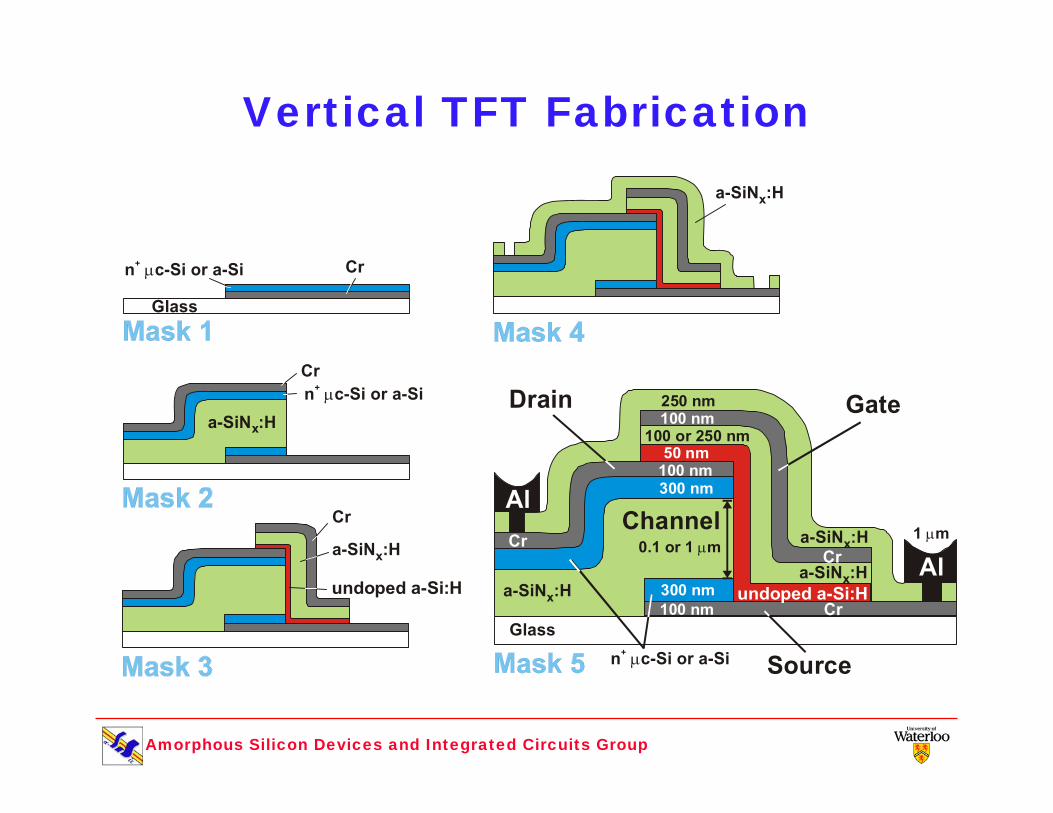
Vertical TFT Fabrication
Glass
Drain
Source
Gate
ChannelAl
Al100 nm300 nm
0.1 or 1 mμ
100 nm50 nm
100 or 250 nm100 nm250 nm
1 mμ
300 nm
Cr
Cr
Cr
a-SiN :Hx
a-SiN :Hx
Cr
a-SiN :HxCr
Cr
undoped a-Si:H undoped a-Si:H
n c-Si or a-Si+ μ
Glass
a-SiN :Hx
a-SiN :Hx
a-SiN :Hx
n c-Si or a-Si+ μ
n c-Si or a-Si+ μ

Amorphous Silicon Devices and Integrated Circuits Group
Mask Mask
Anisotropic EtchingIsotropic Etching
EV
ELSubstrate
EV
Etching of a Substrate Material
Mask Mask(a)
Etching of Multiple Films (endpoint: one possiple case)
MaskMask Mask
Etching of Multiple Films (endpoint: another possible case)
Mask MaskMask Mask
Substrate
Substrate
(b)Mask
MultipleFilms
MultipleFilms
Substrate
Substrate
Vertical Profile Requirements
Mo n+ a-Si:H
n+ a-Si:H
a-SiNx:H
Photoresist
Mo
n+ a-Si:H
n+ a-Si:H
a-SiNx:H
Photoresist
SF6/O2: 50/50, 30s over-etch
Pure SF6, 60s over-etch

Amorphous Silicon Devices and Integrated Circuits Group
Anisotropic Reactive Ion Etching (RIE)
CF4
CFx F
SiF4
CFx
pol
ymer
Glassa-Si:H
Mask Mask
(1) Ion-assisted etching
(4) Sputter removal of polymerfrom horizontal surface
(3) Polymer depositionon vertical surface
(2)
(2) H scavanges F density2
CFx
pol
ymer
e-
CF3+ F-
SiF layerx
e- H2
H
HF
(3)
(4)(1)CFx
Vertical profile
Crn+ a-Si:H
a-SiNx:H
n+ a-Si:H
100 nm300 nm
1 μm
300 nm
CFCF44/H/H22 RIE processRIE process

Amorphous Silicon Devices and Integrated Circuits Group
Structural attributes•All the films in multi-layer vertical structure are fully self-aligned.
•Channel length can be precisely defined - 100 nm in this case but can be scaled down.
Process attributes• Semiconductor and
dielectric films by PECVD; metal films by sputter deposition.
• Vertical channel by RIE.
Vertical Thin Film Transistor
Cr
250
100 250 50
Cr
a - SiNx:H
100
300
100
300
Gate
Drain
Channel Source
n + a - Si :H
Gate
100
a - SiN x :H un. a- Si :H
n + a - Si :H
Cra - SiN x :H
400
200
(Values in nm)
Chan, Nathan, APL, vol. 86 (2005) 253501

Amorphous Silicon Devices and Integrated Circuits Group
Transfer and I-V CharacteristicsTransfer and I-V Characteristics
-10 -5 0 5 10 15 2010-16
10-14
10-12
10-10
10-8
10-6
10-4
n+ μc-Si:HtSiNx = 250 nm
0.5
4.5VD (V)(1 V/step)
W/L = 11/0.1 (μm)
S = 0.8 V/decVT = 2.8 VON/OFF ratio > 108IOFF = 10-15 AAt VD = 1.5 V:
μFE = 0.052 cm2/Vs
I D (A
)
VG (V) 0 1 2 3 4 5 60
2
4
6
8
10
12
14
16
18
n+ μc-Si:H
W/L = 11/0.1 (μm)tSiNx = 250 nm
05
10
15
20VG (V)
I D (μA
)VD (V)
~0.8Sub-threshold Slope (V/dec)~2.8Threshold Voltage (V)~1OFF Current (fA)
> 10ON Current (μA)> 108ON/OFF Current Ratio
ValuesVDS = 0.5 V
0 5 10 15 200
2
4
6
8
10
12
14
16
18
510
15
20
25
30VG (V)
n+ μc-Si:HtSiNx = 250 nmW = 100/1 (μm)
I D (μA
)VD (V)

Amorphous Silicon Devices and Integrated Circuits Group
0.0 0.2 0.4 0.6 0.8 1.0
0
2
4
6
8
10
12
tSiNx:H= 50 nm
Normalized Distance from Drain
Inte
rfac
e Po
tent
ial [
V]
VG= 12 V
Back VD= 10 VVD= 0.1 VFront
L=100 nm
ta-Si= 25 nm
Lack of Gate Control
VTFT Short Channel Issues
0 2 4 6 8 100
10
20
30
40
50
n+ μc-Si:H
tSiNx = 50 nmW/L = 100/0.1 (μm) VG (V) 30
25
20
510
15
Dra
in C
urre
nt (μ
A)
Drain Voltage (V)
Possible Solutions• Decrease gate dielectric thickness for better
gate control - Cgate, Igate!• Use double gate structure and ground 2nd
gate• Sandwich a p+ layer to n+ S/D – halo doping
0.0 0.2 0.4 0.6 0.8 1.0
0
2
4
6
8
10
12
Normalized Distance from Drain
Inte
rfac
e Po
tent
ial [
V]
VG= 0 V
Back
tSiNx:H= 50 nm
VD= 10 VVD= 0.1 VFront
L=100 nm
ta-Si= 25 nm

Amorphous Silicon Devices and Integrated Circuits Group
Source Drain
Vertical ChannelW/L = 20/0.1 (μm)
10 μm
0.333 μm/div
Gate
2 μm
Total gate overlap area
NMOS NMOS VTFT VTFT
inverterinverterVin T2
T1
VDD
Vout
-5 0 5 10 15
50
60
70
80
90
100
10 kHzAC signal
TFT size: 10 μm x 10 μm
CG-SD = 48 fF
n+ μc-Si:HtSiNx = 125 nmW/L = 20/0.1 (μm)
100 kHz
Tota
l Gat
e In
put C
apac
itanc
e (fF
)
Gate Voltage (V)-4 -3 -2 -1 0 1 2 3 4
0
1
2
3
4 W/L = 40/0.1 (μm)3
2
1
VDD = 4 (V)
Out
put V
olta
ge, V
out (
V)
Input Voltage, Vin (V)
C-V and NMOS Inverter CharacteristicsC-V and NMOS Inverter Characteristics
VTFT VTFT top top
viewview
Lateral TFT – 3 µm DRCG-SD ~ 15 pF
Amorphous Silicon Devices and Integrated Circuits Group
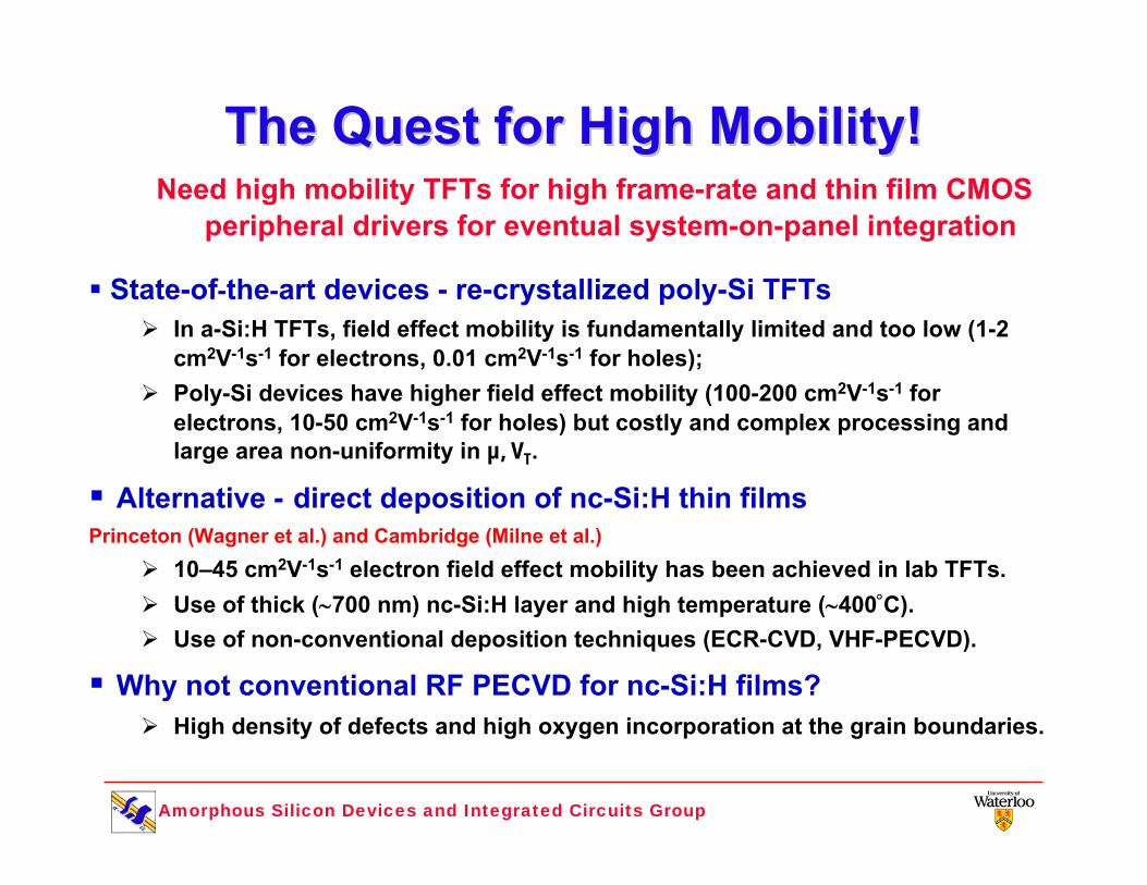
The Quest for High Mobility!The Quest for High Mobility!Need high mobility TFTs for high frame-rate and thin film CMOS
peripheral drivers for eventual system-on-panel integration
State-of-the-art devices - re-crystallized poly-Si TFTsIn a-Si:H TFTs, field effect mobility is fundamentally limited and too low (1-2 cm2V-1s-1 for electrons, 0.01 cm2V-1s-1 for holes);Poly-Si devices have higher field effect mobility (100-200 cm2V-1s-1 for electrons, 10-50 cm2V-1s-1 for holes) but costly and complex processing and large area non-uniformity in µ, VT.
Alternative - direct deposition of nc-Si:H thin films Princeton (Wagner et al.) and Cambridge (Milne et al.)
10–45 cm2V-1s-1 electron field effect mobility has been achieved in lab TFTs.Use of thick (∼700 nm) nc-Si:H layer and high temperature (∼400°C).Use of non-conventional deposition techniques (ECR-CVD, VHF-PECVD).
Why not conventional RF PECVD for nc-Si:H films?High density of defects and high oxygen incorporation at the grain boundaries.

Amorphous Silicon Devices and Integrated Circuits Group
Nucleation phase
Steady stateGrowth phase
Incubation layerSubstrate
Gate Dielectric
Substrate
Gate Metal
DS
Top-gate TFTs - higher mobility (quasi poly-Si structure)
Gate Dielectric
SubstrateGate Metal
DS
Bottom-gate TFTs - lower mobility (quasi a-Si:H structure)
If If grain sizegrain size << << channel lengthchannel length Uniform device characteristicsUniform device characteristics (V(VTT, I, IONON, I, IOFFOFF, , µµFEFE) over large area. ) over large area. But will we get sufficient grain boundary But will we get sufficient grain boundary passivationpassivation??
REQUIREMENTS FOR HIGH MOBILITYLow defect density & high crystallinity channelThin incubation layer for bottom gate TFTsHigh surface smoothness channel for top-gate TFT Thin channel layers to reduce series resistance High conductivity contact layers to reduce S/D contact resistanceHigh quality gate dielectric with good interface integrity

Amorphous Silicon Devices and Integrated Circuits Group
0 50 100 150 200 250 300 35010-10
10-9
10-8
10-7
10-6
10-5
H2/(SiH4 + H2)=99 %
Cry
stal
line
Vol
ume
Frac
tion
(%)
Dar
k C
ondu
ctiv
ity (S
/cm
)
Film Thickness (nm)
40
50
60
70
80
90
100
20 30 40 50 60 70 80
300 nm nc-Si:Hgrain size 25-30 nm
<222><111>
Inte
nsity
(a.u
.)
Degree (2θ)
PECVD PECVD ncnc--Si:HSi:H Films: Growth Rate and Films: Growth Rate and CrystallinityCrystallinity
95 96 97 98 99 1002
3
4
5
6
7
8
9
Cry
stal
line
Volu
me
Frac
tion
(%)
Gro
wth
Rat
e (n
m/m
in)
H2 / (SiH4 + H2) (%)
70
75
80
85
100 nm thick film
99 % dilution, growth rate 2.7 nm/min, Xc 80–82 % σdark~10-6 S/cm, Xc~85 %
High density of atomic hydrogen in the plasma favors etching weak Si-Si bonds.
High hydrogen surface coverage promotes structural ordering onto stable nucleation sites at the growth surface.
►► Controlled Controlled depdep of hof high igh crystallinitycrystallinity thin thin ncnc--Si:HSi:H film seems achievable!film seems achievable!
Standard 13. 56 MHz PlasmaTherm 790
Lee et al., APL, vol. 86 (2005) 222106 and Virtual J. Nanoscale Science & Technology vol. 11, 2005

Amorphous Silicon Devices and Integrated Circuits Group
RF PECVD nc-Si:H Film Microstructure
Dense columnar-like growth
Amorphous incubation layer (~5nm)
Glass substrate
TEM Cross-Section Raman Spectrum
400 450 500 550 600
nano phase ~500 cm-1
amorphous phase ~480 cm-1
crystalline phase ~520 cm-1
H2 / (H2 + SiH4)= 99 %Raman crystallinity ~ 85 %
Nor
mal
ized
Inte
nsity
(a.u
.)
Raman Shift (cm-1)
film thickness ~ 300 nm
Electron diffraction patterns - central bright circular region <111> and <220> rings and weak <311> rings with diffraction spots.
TEM, Raman and XRD all confirm high crystallinity
Amorphous Silicon Devices and Integrated Circuits Group
0 100 200 300 400 500 6001016
1017
1018
1019
1020
1021
1022
H2/(SiH4 + H2) = 99 %
Oxygen
nc-Si:H film c-Si substrate
Hydrogen
Con
cent
ratio
n (a
t./cm
3 )
Depth (nm)
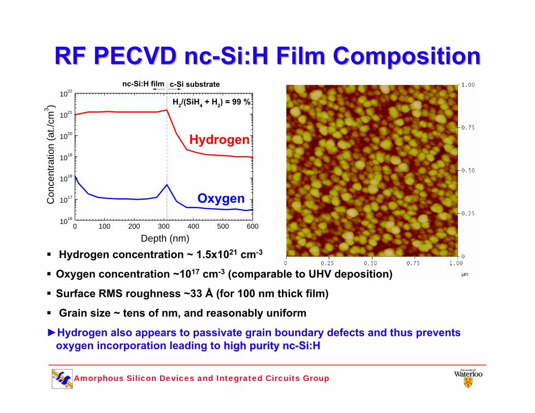
Hydrogen concentration ~ 1.5x1021 cm-3
Oxygen concentration ~1017 cm-3 (comparable to UHV deposition)
Surface RMS roughness ~33 Å (for 100 nm thick film)
Grain size ~ tens of nm, and reasonably uniform
►Hydrogen also appears to passivate grain boundary defects and thus prevents oxygen incorporation leading to high purity high purity ncnc--Si:HSi:H
RF PECVD RF PECVD ncnc--Si:HSi:H Film CompositionFilm Composition

Amorphous Silicon Devices and Integrated Circuits Group
Top Gate nc-Si:H TFTs with a-SiOx
-8 -7 -6 -5 -4 -3 -2 -1 00.0
0.5
1.0
1.5
2.0
VDS = - 3 V
VDS = - 4 V
VDS = - 5 V
W / L = 200 μm / 50 μm
Dra
in-S
ourc
e C
urre
nt (
μA
)
Drain-Source Voltage (V)0 1 2 3 4 5 6 7 8
0
10
20
30
40
VGS = 3 V
VGS = 5 V
VGS = 4 V
W / L = 200 μm / 50 μm
Dra
in-S
ourc
e C
urre
nt (μ
A)
Drain-Source Voltage (V)
P-channel TFT N-channel TFT
Onset of lateral p-n diode formation at |VDS| > |VGS| - |VT|
glassnc-Si:Ha-SiOx
AlAl Al 50 nm nc-Si:H/Cr
S/D silicidedohmic contact
300 nm300 nm
90 nm
glassnc-Si:Ha-SiOx
AlAl Al 50 nm nc-Si:H/Cr
S/D silicidedohmic contact
300 nm300 nm
90 nma-SiO
Al
Cr CrDrainSource
Gate
x
nc-Si:Helectronsholes

Amorphous Silicon Devices and Integrated Circuits Group
-10 -9 -8 -7 -6 -5 -4 -3 -2 -1 0 1 210-13
10-12
10-11
10-10
10-9
10-8
10-7
10-6
10-5
10-4
Fiel
d-E
ffect
Mob
ility
(cm
2 /Vs)W / L = 200 μm / 50 μm
VSD = -1 V
Sou
rce-
Dra
in C
urre
nt (
A )
Gate-Drain Voltage (V)
0
10
20
30
40
VDS = -1 V
μeFE ~150 cm2/VsVT ~1.8 V
S ~0.3 V/dec
TFT Transfer Characteristics
-3 -2 -1 0 1 2 3 4 5 6 7 810-13
10-12
10-11
10-10
10-9
10-8
10-7
10-6
10-5
10-4
W / L = 200 μm / 50 μm VDS = 1 V
Dra
in-S
ourc
e C
urre
nt (A
)
Gate-Source Voltage (V)
0
50
100
150
200
Fiel
d-E
ffect
Mob
ility
(cm
2 / V
s)PMOS
μhFE ~25 cm2/VsVT ~ -3.8 V
S ~0.25 V/dec
NMOSg m
L/(W
CO
XVD
S) (
cm2 /V
s)
g mL/
(WC
OXV
DS) (
cm2 /V
s)

Amorphous Silicon Devices and Integrated Circuits Group
0 2 4 6 80
2
4
6
8
10
0
2
4
6
8
10
Out
put V
olta
ge G
ain
VDD = 8 V
Out
put V
olta
ge (V
)
Input Voltage (V)
CMOS Inverter
VOUT
VDD
VIN
VSS
P
N
PMOS: 200µm/50µm
NMOS: 200µm/100µm
Output voltage gain: 7.2

Amorphous Silicon Devices and Integrated Circuits Group
• Vertical thin film transistors based on a well-defined and reproducible vertical device structure: ON/OFF current ratio ~108, threshold voltage ~2.8V, and sub-threshold slope of ~0.8 V/dec. Device can be easily scaled to sub-100 nm channel lengths but need device optimization to reduce short channel effects.
• Direct deposition of nc-Si:H using standard 13.56 MHz PECVD from 99 % H2 diluted SiH4 yields high purity and high crystallinitync-Si:H thin films.
• Ambipolar TFTs made of nc-Si:H show n-channel mobility about 150 cm2V-1s-1 and p-channel mobility of 30 cm2V-1s-1. Highest reported to-date and first demonstration of PECVD CMOS.
• Integration approaches presented are very promising for x-ray imaging and displays with extremely high fill factor and resolution, as well as for system-on-panel integration!
Conclusions