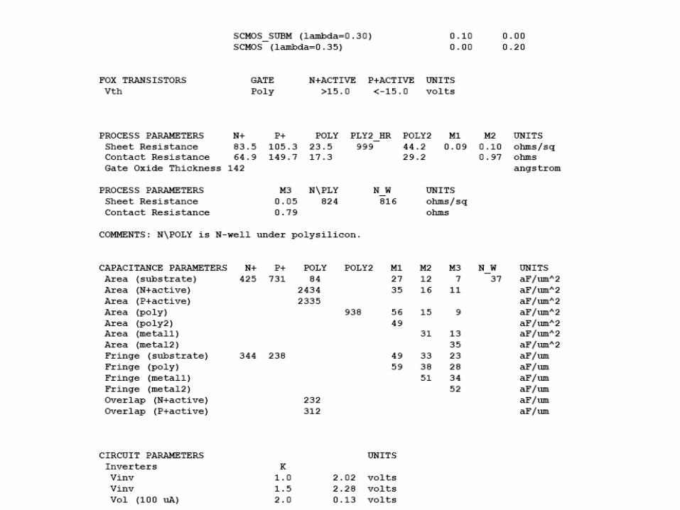
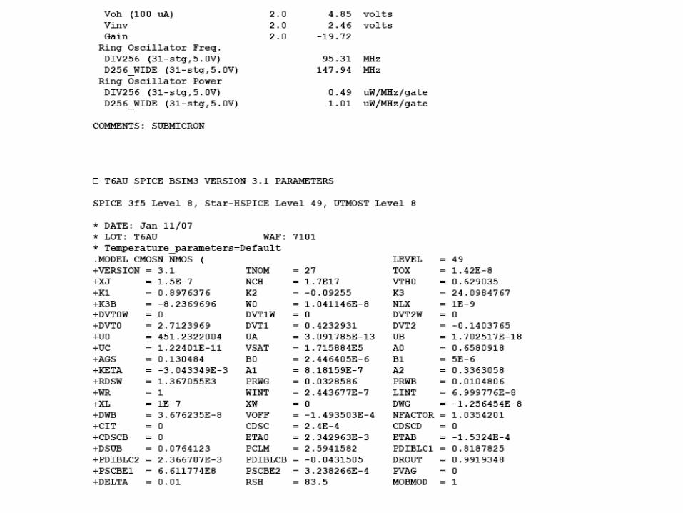
devices in semiconductor processes resistorsclass.ece.iastate.edu/ee330/lectures/ee 330 lect 10 fall...
TRANSCRIPT

9911 22 55 6633 44 8877
11
22
33
44
55
66
EE 330 Fall 2016 Seating
Bailey Akers
Brandon Baxter
Zachary Bennett
Jose Candelario
Aurelien Chanel
Alexander Christenson
David Clark
Benjamin Engebrecht
Benjamin Gisler
Daniel Griffen
William Henthorn
Jakub Hladik
Sarah Huber
Abdelmagieed Ibrahim
Jacob Johnson
James Kluesner
Jinan Li
Xiang Li
Timothy Lindquist
Christopher Little
Shengxin Mao
Matthew Martinez
Travis Merrifield
Eric Middleton
Joshua Pachl
Milan Patel
Li Qian
Yi Qiu
Matthew Rottinghaus
Sandra Sebastian
Robert Slezak
Nathaniel Summitt
Steve Ukpan
Dean Vanevery
Steven Warren
Brian Weber
Jiangning Xiong
Chenhang Xu
Jie-Hui Yan
Yuxuan Yuan
Austin Yurchik
Benjamin Zickefoose
77
Karla Beas
Sang Uk Park
Apurba Kumar Das
Liang Zhang
Amna Aftab

EE 330
Lecture 10
IC Fabrication Technology
Part III
- Parasitic Capacitances
- Back-end Processes
Devices in Semiconductor Processes
Resistors
Diodes

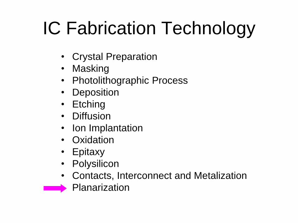
IC Fabrication Technology
• Crystal Preparation
• Masking
• Photolithographic Process
• Deposition
• Etching
• Diffusion
• Ion Implantation
• Oxidation
• Epitaxy
• Polysilicon
• Planarization
• Contacts, Interconnect and Metalization
Review from Last Lecture

Copper Interconnects
Limitations of Aluminum Interconnects
• Electromigration
• Conductivity not real high
Relevant Key Properties of Copper
• Reduced electromigration problems at
given current level
• Better conductivity
Challenges of Copper Interconnects• Absence of volatile copper compounds
(does not etch)
• Copper diffuses into surrounding
materials (barrier metal required)
Review from Last Lecture

Patterning of CopperDamascene Process
Copper DepositionW-plug
CMP Target
Copper is deposited or electroplated (Barrier Metal Used for Electroplating Seed)
Review from Last Lecture
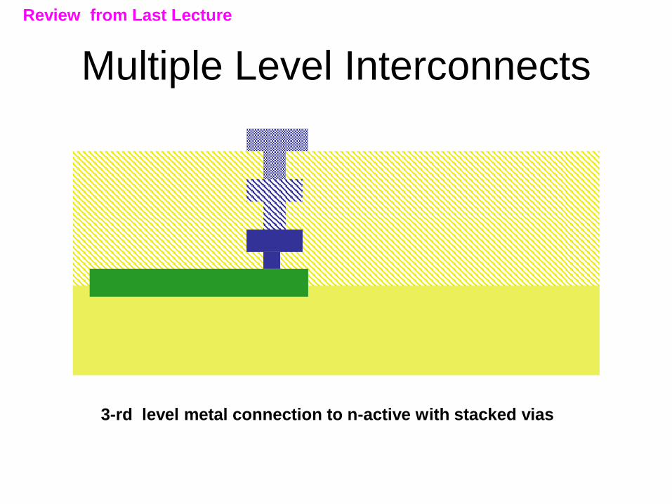
Multiple Level Interconnects
3-rd level metal connection to n-active with stacked vias
Review from Last Lecture
Metalization
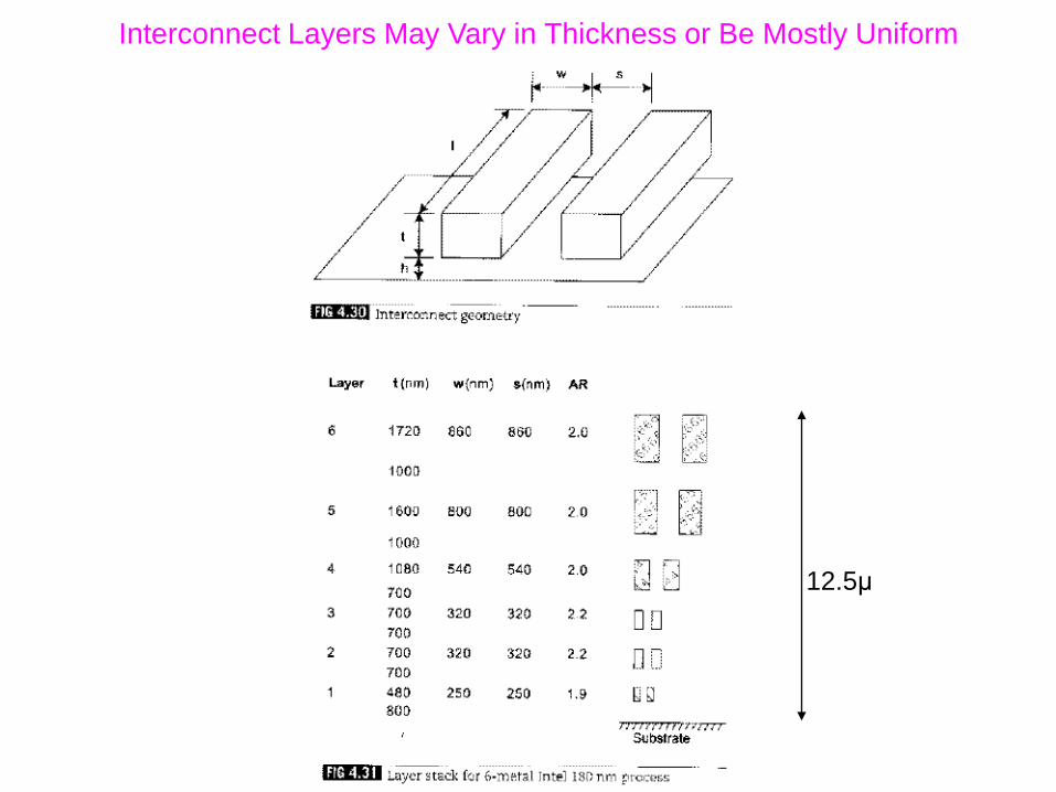
Interconnect Layers May Vary in Thickness or Be Mostly Uniform
12.5μ
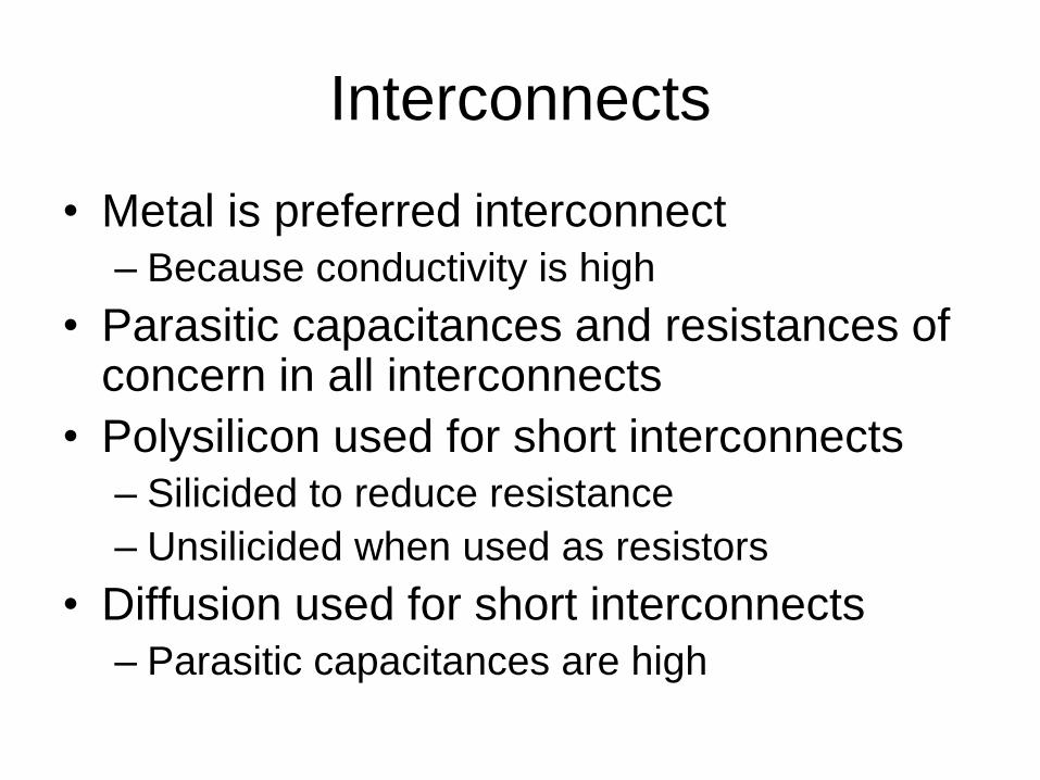
Interconnects
• Metal is preferred interconnect
– Because conductivity is high
• Parasitic capacitances and resistances of concern in all interconnects
• Polysilicon used for short interconnects
– Silicided to reduce resistance
– Unsilicided when used as resistors
• Diffusion used for short interconnects
– Parasitic capacitances are high
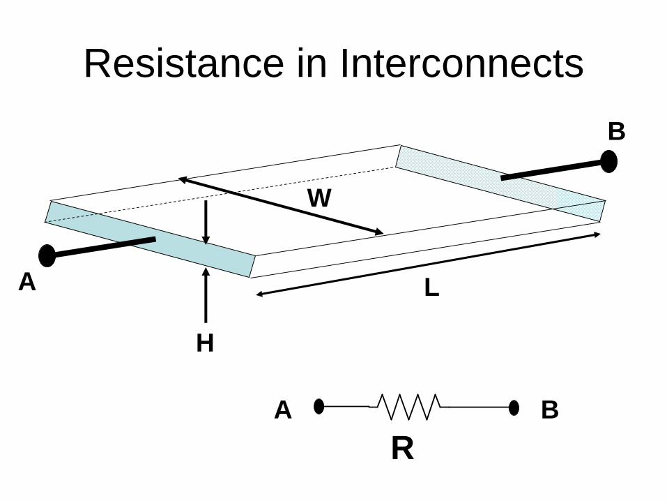
Resistance in Interconnects
L
W
H
A
B
BA
R

Resistance in Interconnects
L
W
HA
B
BD
R
D
ρA
LR
A=HW
ρ independent of geometry and
characteristic of the process
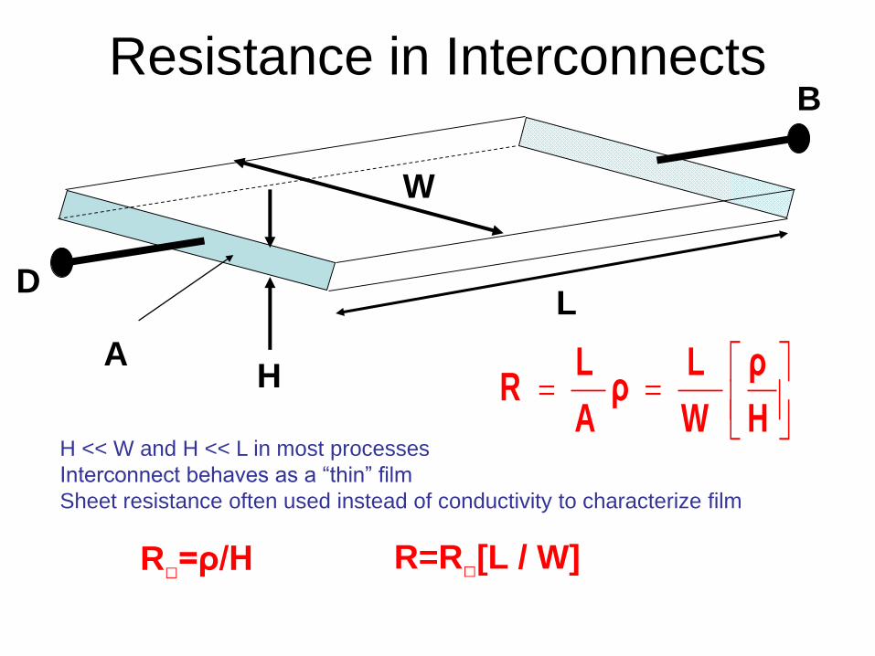
Resistance in Interconnects
L
W
HA
B
D
H
ρ
W
Lρ
A
LR
H << W and H << L in most processes
Interconnect behaves as a “thin” film
Sheet resistance often used instead of conductivity to characterize film
R□=ρ/H R=R□[L / W]
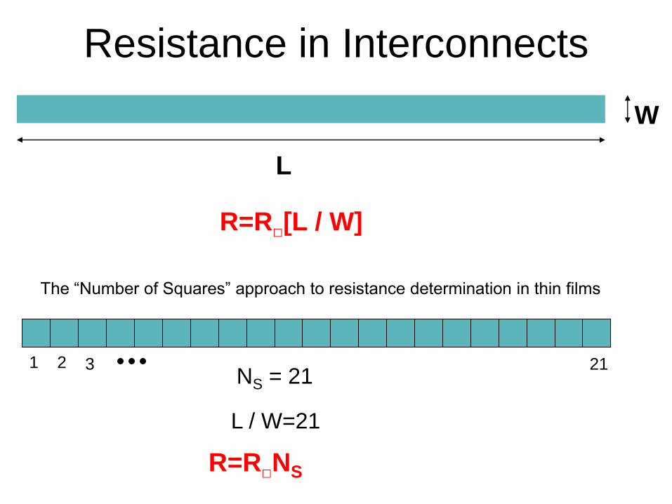
Resistance in Interconnects
R=R□[L / W]
L
W
The “Number of Squares” approach to resistance determination in thin films
1 2 3 21NS = 21
L / W=21
R=R□NS
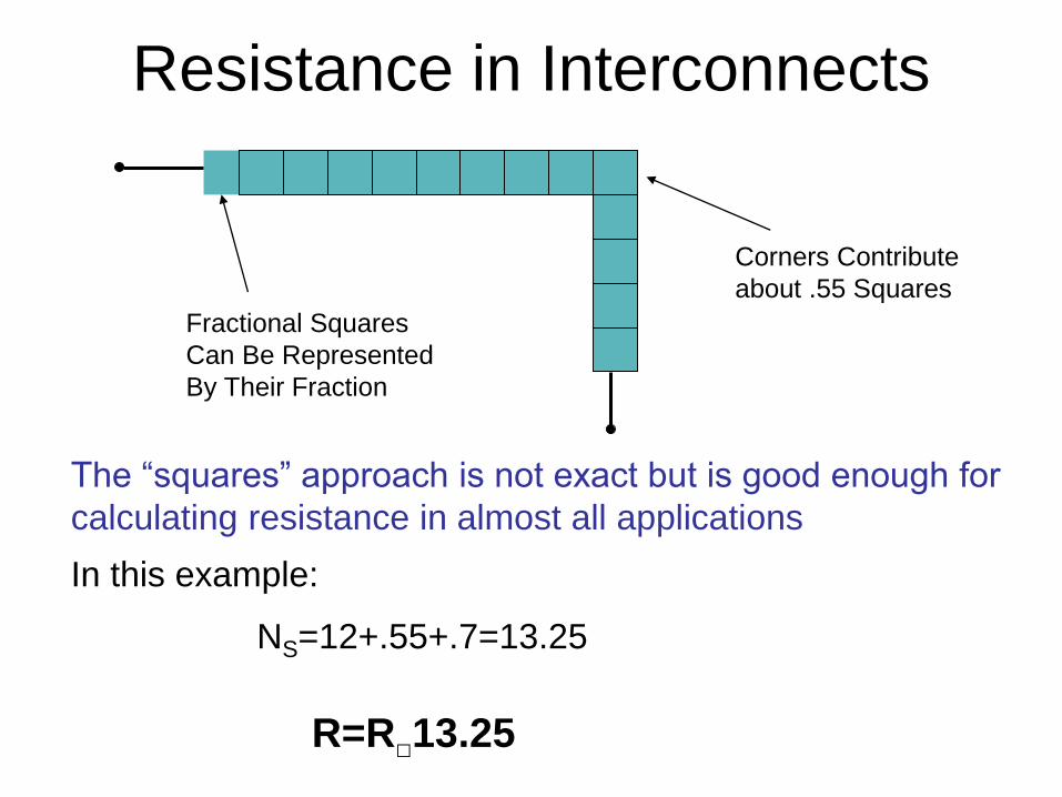
Resistance in Interconnects
R=R□13.25
Corners Contribute
about .55 Squares
Fractional Squares
Can Be Represented
By Their Fraction
In this example:
NS=12+.55+.7=13.25
The “squares” approach is not exact but is good enough for
calculating resistance in almost all applications
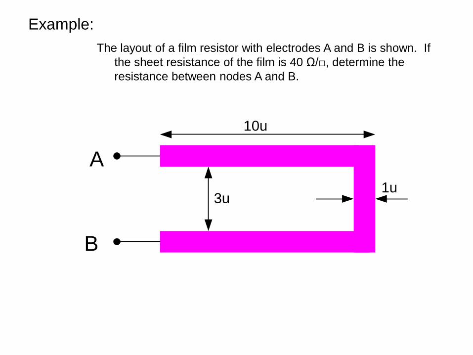
Example:
The layout of a film resistor with electrodes A and B is shown. If
the sheet resistance of the film is 40 Ω/□, determine the
resistance between nodes A and B.
10u
3u1u
A
B
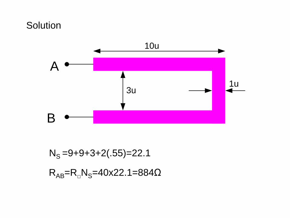
10u
3u1u
A
B
Solution
NS =9+9+3+2(.55)=22.1
RAB=R□NS=40x22.1=884Ω
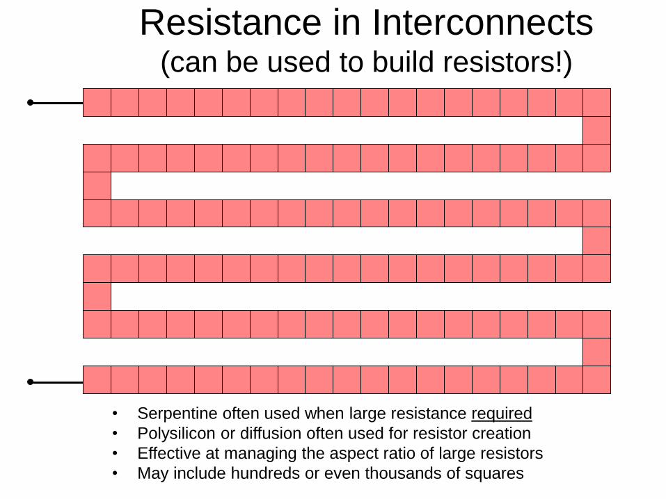
Resistance in Interconnects(can be used to build resistors!)
• Serpentine often used when large resistance required
• Polysilicon or diffusion often used for resistor creation
• Effective at managing the aspect ratio of large resistors
• May include hundreds or even thousands of squares

Resistance in Interconnects(can be used to build resistors!)
d1
2d
2
Area requirements determined by both minimum
width and minimum spacing design rules
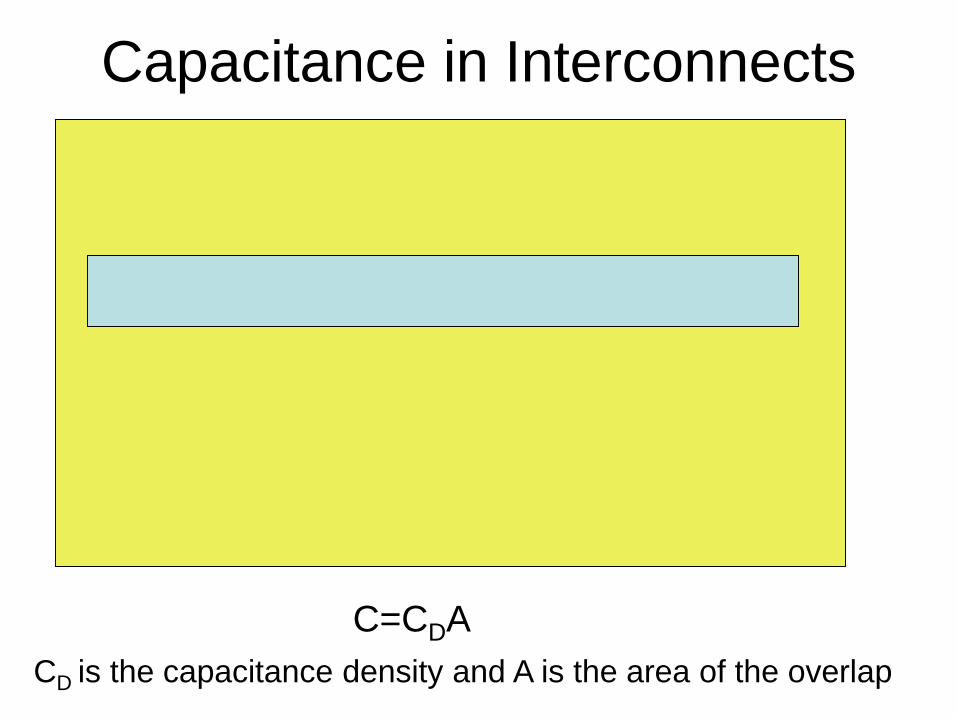
Capacitance in Interconnects
C=CDA
CD is the capacitance density and A is the area of the overlap
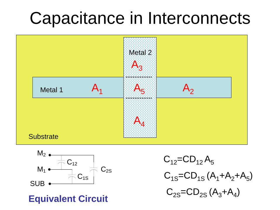
Capacitance in Interconnects
Metal 1
Metal 2
Substrate
A1
A4
A2
A3
A5
C12
C2S
C1S
M1
M2
SUB
Equivalent Circuit
C12=CD12 A5
C1S=CD1S (A1+A2+A5)
C2S=CD2S (A3+A4)
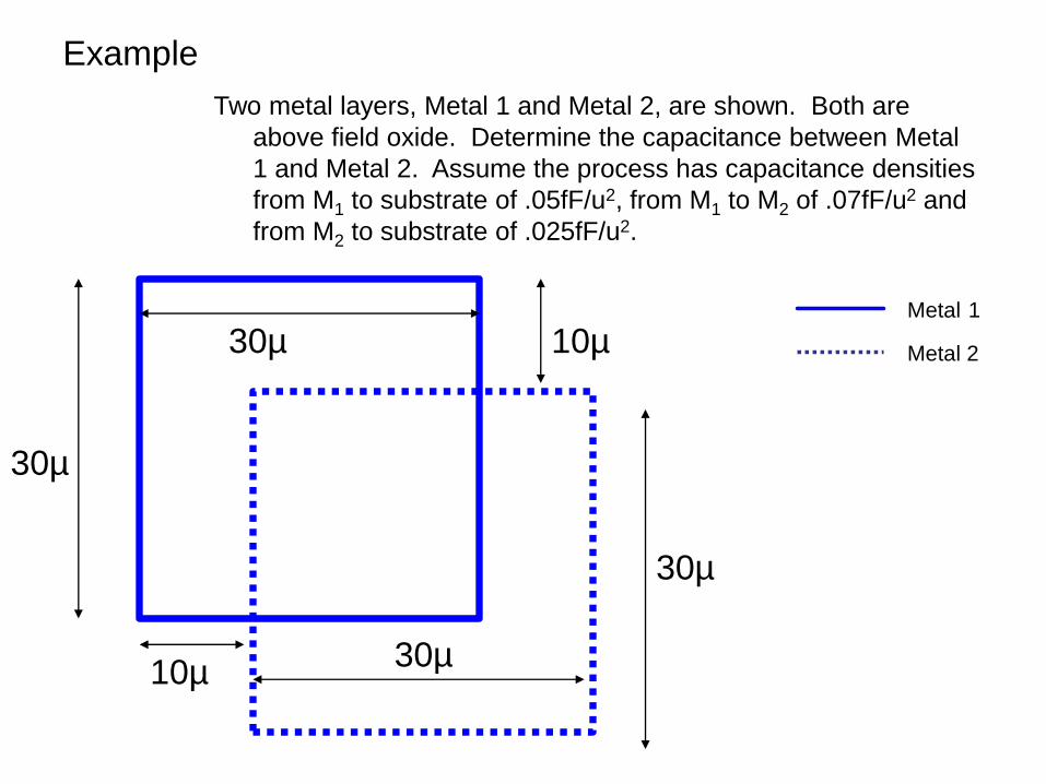
Example
Two metal layers, Metal 1 and Metal 2, are shown. Both are
above field oxide. Determine the capacitance between Metal
1 and Metal 2. Assume the process has capacitance densities
from M1 to substrate of .05fF/u2, from M1 to M2 of .07fF/u2 and
from M2 to substrate of .025fF/u2.
30µ
30µ
30µ
30µ
10µ
10µ
Metal 1
Metal 2
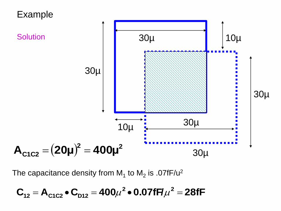
Example
The capacitance density from M1 to M2 is .07fF/u2
30µ
30µ
30µ
30µ
10µ
10µ
Solution
30µ
22
C1C2 400μ20μA
28fF0.07fF/400CAC 22
D12C1C212

Capacitance and Resistance in
Interconnects
• See MOSIS WEB site for process
parameters that characterize parasitic
resistances and capacitances
www.mosis.org


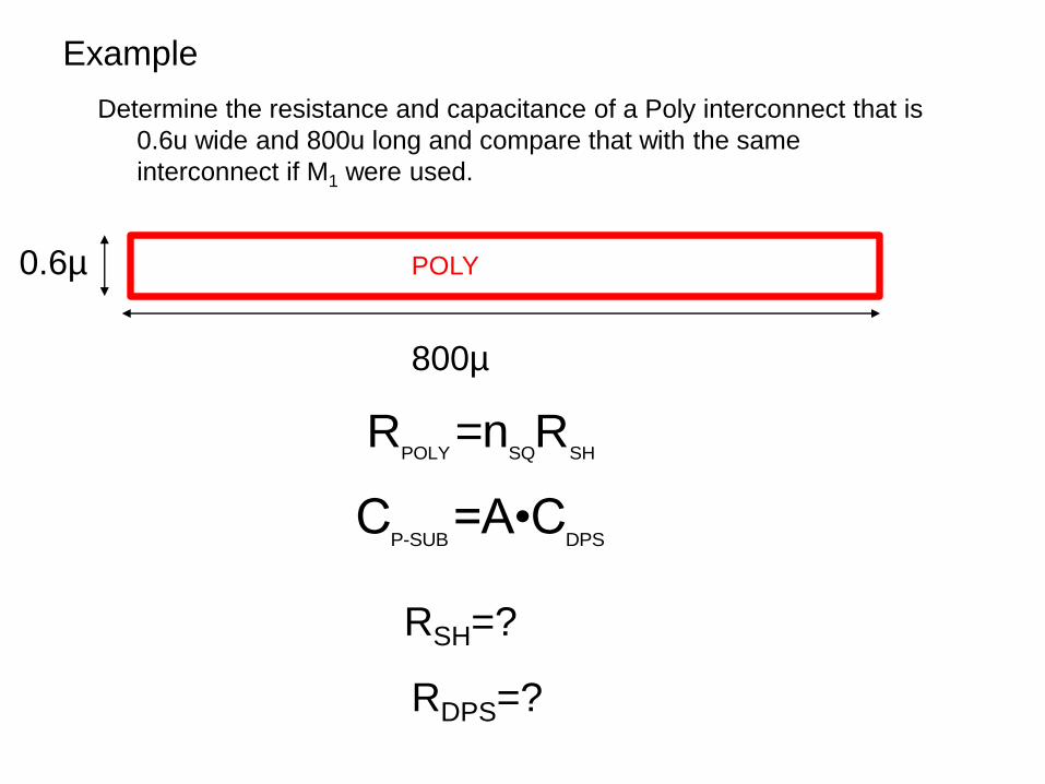
Example
Determine the resistance and capacitance of a Poly interconnect that is
0.6u wide and 800u long and compare that with the same
interconnect if M1 were used.
0.6µ
800µ
POLY
POLY SQ SHR =n R
P-SUB DPSC =A•C
RSH=?
RDPS=?

RSH=23.5Ω/□
CDPS=84 af/µ2

Example
Determine the resistance and capacitance of a Poly interconnect that is
0.6u wide and 800u long and compare that with the same
interconnect if M1 were used.
0.6µ
800µ
8001333
0 6.SQ
n
20 6 800 480A= .
POLY SQ SHR =n R =23.5•1333=31.3KΩ
2 -2
P-SUB DPSC =A•C =480μ •84aFμ =40.3fF
POLY

Example
Determine the resistance and capacitance of a Poly interconnect that is
0.6u wide and 800u long and compare that with the same
interconnect if M1 were used.
0.6µ
800µ
Metal 1

RSH=0.09Ω/□
CDPS=27 af/µ2

Example
Determine the resistance and capacitance of a Poly interconnect that is
0.6u wide and 800u long and compare that with the same
interconnect if M1 were used.
0.6µ
800µ
8001333
0 6.SQ
n
20 6 800 480A= .
M1 SQ SHR =n R =0.09•1333=120Ω
2 -2
M1-SUB DM1SC =A•C =480μ •27aFμ =13.0fF
Metal 1
IC Fabrication Technology
• Crystal Preparation
• Masking
• Photolithographic Process
• Deposition
• Etching
• Diffusion
• Ion Implantation
• Oxidation
• Epitaxy
• Polysilicon
• Contacts, Interconnect and Metalization
• Planarization

Planarization
• Planarization used to keep surface planar
during subsequent processing steps
– Important for creating good quality layers in
subsequent processing steps
– Mechanically planarized
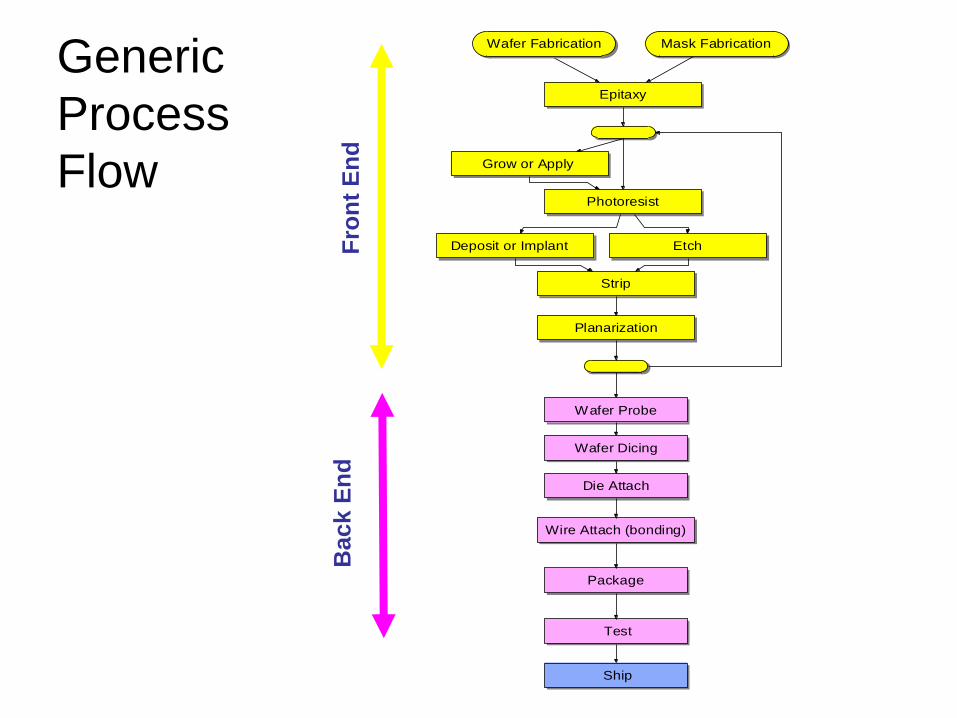
Mask Fabrication
Epitaxy
Photoresist
Etch
Strip
Planarization
Deposit or Implant
Grow or Apply
Wafer Probe
Die Attach
Wafer Dicing
Wire Attach (bonding)
Package
Test
Wafer Fabrication
Ship
Fro
nt
En
dB
ack E
nd
Generic
Process
Flow

Front End Process Integration for Fabrication of ICs
Wafer Fabrication Mask Fabrication
Epitaxy
Photoresist
Deposit or Implant Etch
Strip
Planarize
Back End Processing
On
ce
fo
r e
ach
ma
sk
Front-End Process Flow
• Front-end processing steps analogous to a
“recipe” for manufacturing an integrated
circuit
• Recipes vary from one process to the next
but the same basic steps are used
throughout the industry
• Details of the recipe are generally
considered proprietary

Back-End Process Flow
Wafer Probe
Die Attach
Wafer Dicing
Wire Attach (bonding)
Package
Test
Ship

Wafer Dicing
www.renishaw.com
Die Attach
1. Eutectic
2. Pre-form
3. Conductive Epoxy
Electrical Connections (Bonding)
• Wire Bonding
• Bump Bonding

Wire Bonding
Wire – gold or aluminum
25 in diameter

Wire Bonding
Excellent Annimation showing process at :
http://www.kns.com/_Flash/CAP_BONDING_CYCLE.swf

Wire Bonding
www.kns.com
Ball Bond
Wedge Bond
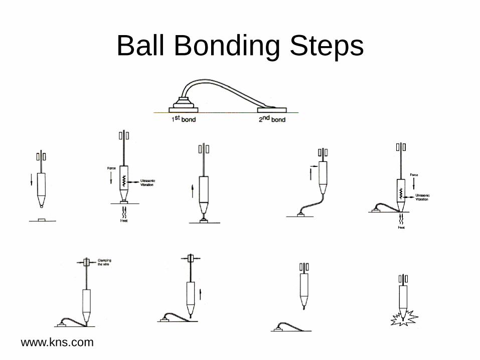
Ball Bonding Steps
www.kns.com

Ball Bonding Tip
Approx 25µ
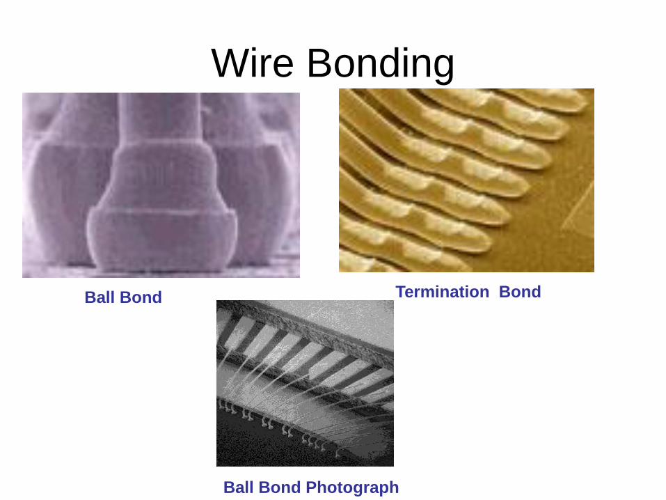
Wire Bonding
Ball Bond Termination Bond
Ball Bond Photograph
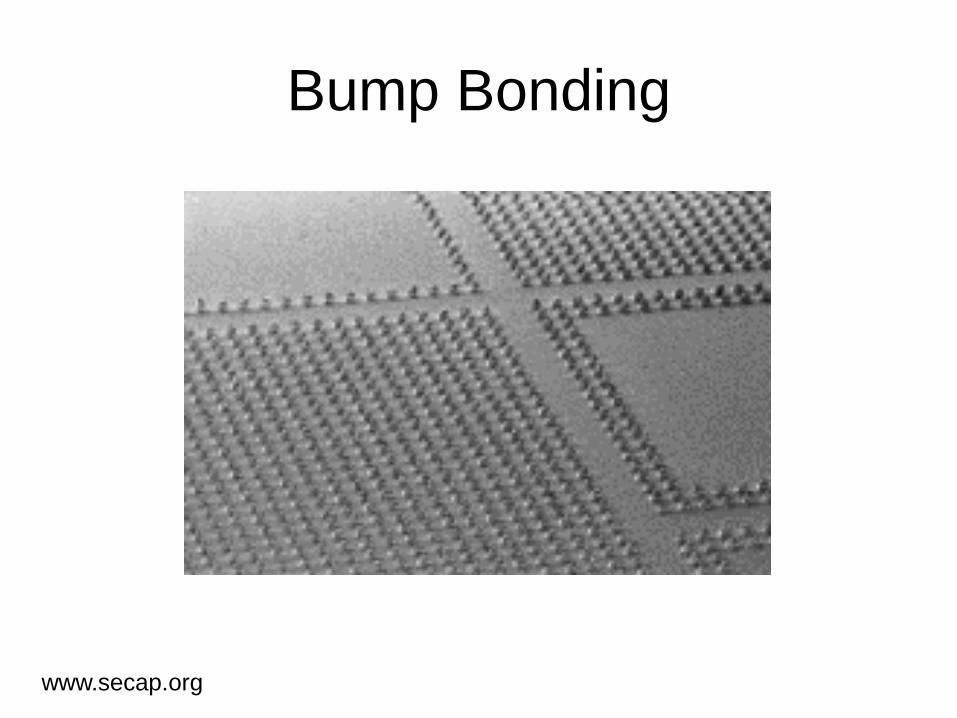
Bump Bonding
www.secap.org

End of Lecture 10