ee 203 lecture 12 - iowa state universityclass.ece.iastate.edu/ee330/lectures/ee 330 lect 43... ·...
TRANSCRIPT

EE 330
Lecture 43
Digital Circuits
• Other Logic Styles
• Dynamic Logic Circuits
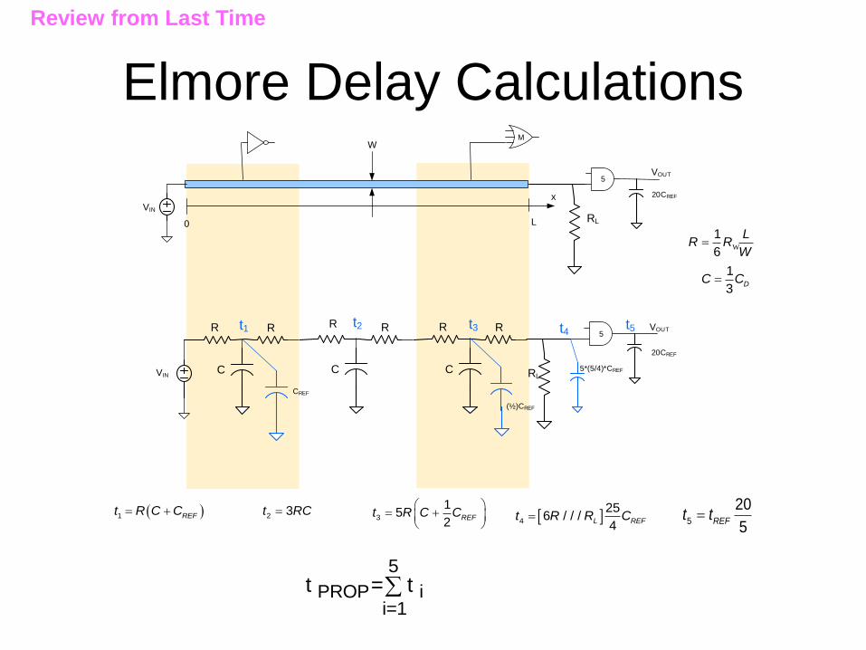
Elmore Delay Calculations
L
x
0
VIN
RL
VOUT
M
5
20CREF
R
C
R R
C
R R
C
R
RL
VOUT5
20CREF
5*(5/4)*CREF
CREF
(½)CREF
VIN
t1 t2 t3 t4 t5
W
1
6
LR R
W
W
1
3DC C
1 REFt R C C 2 3t RC 4
256 / / /
4L REFt R R C3
15
2REFt R C C
5
20
5REFt t
5
PROP ii=1
t = t
Review from Last Time
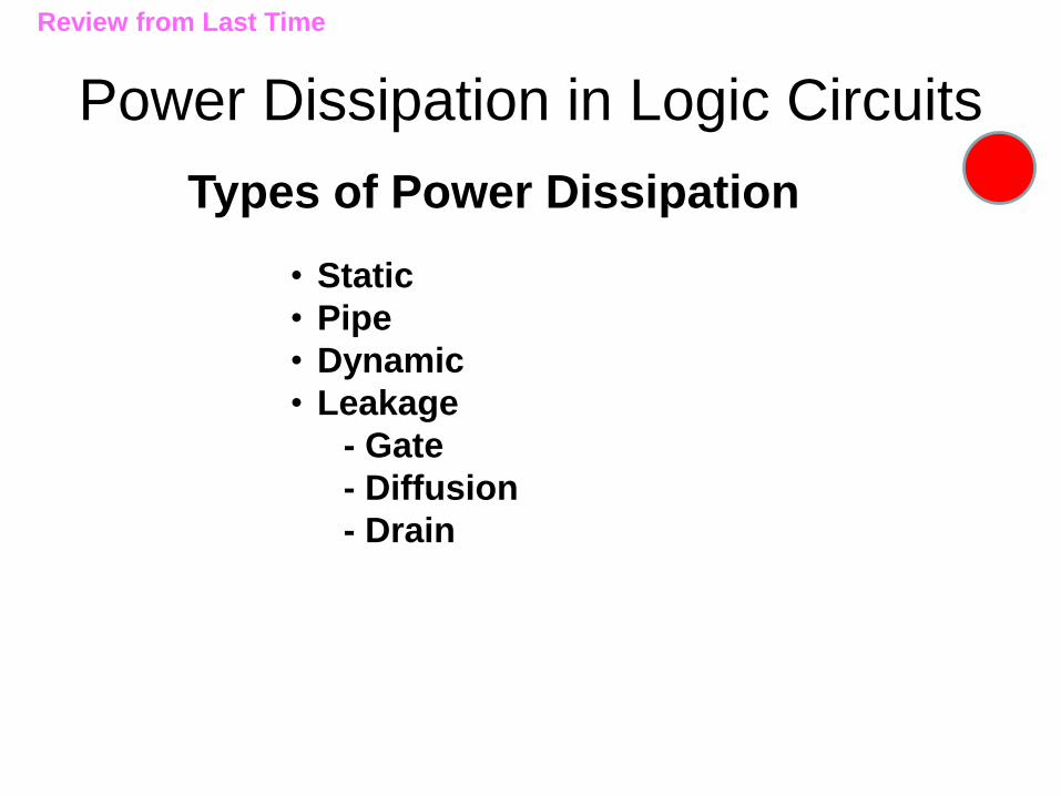
Power Dissipation in Logic Circuits
Types of Power Dissipation
• Static
• Pipe
• Dynamic
• Leakage
- Gate
- Diffusion
- Drain
Review from Last Time

Dynamic Power DissipationVDD
F
A
IDD
CL
RPU
RPD
VC2DYN CL DD
P =f V
The clock transitions on every clock cycle (i.e. it has a transition duty cycle of 100%)
2CLDYN L DD
fP = C V
2
Clock distribution can cause significant power dissipation
Energy dissipated with clock signal itself
But if a gate has a transition duty cycle of 50% with a clock frequency of fCL
Review from Last Time

Leakage Power Dissipation- Gate
• with very thin gate oxides, some gate
leakage current flows
• major concern in 60nm and smaller
processes
• actually a type of static power dissipation
-Diffusion• Leakage across a reverse-biased pn junction
• Dependent upon total diffusion area
• May actually be dominant power loss on longer-
channel devices
• Actually a type of static power dissipation
-Drain
• channel current due to small VGS-VT
• of significant concern only with low VDD
processes
• actually a type of static power dissipation
Gate
Gate
IGLEAK
IDLEAK
Long Channel Device
Short Channel Device
IDIFFUSION
IDIFFUSION
Review from Last Time
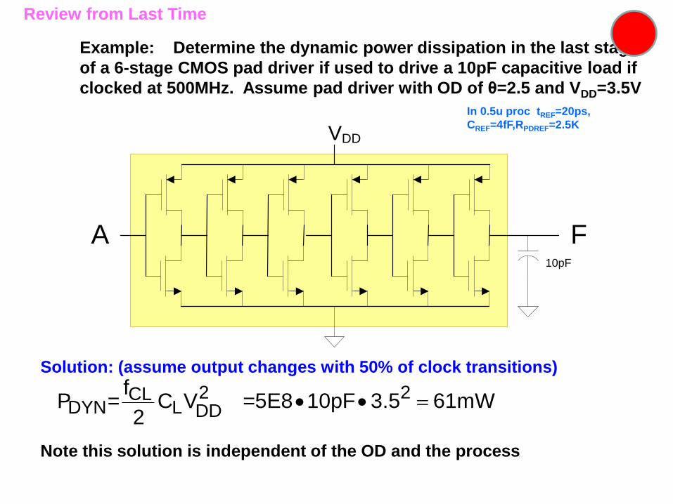
A F
VDD
10pF
Example: Determine the dynamic power dissipation in the last stage
of a 6-stage CMOS pad driver if used to drive a 10pF capacitive load if
clocked at 500MHz. Assume pad driver with OD of θ=2.5 and VDD=3.5V
Solution: (assume output changes with 50% of clock transitions)
In 0.5u proc tREF=20ps,
CREF=4fF,RPDREF=2.5K
2CLDYN L DD
fP = C V
2
2=5E8 10pF 3.5 61mW
Note this solution is independent of the OD and the process
Review from Last Time
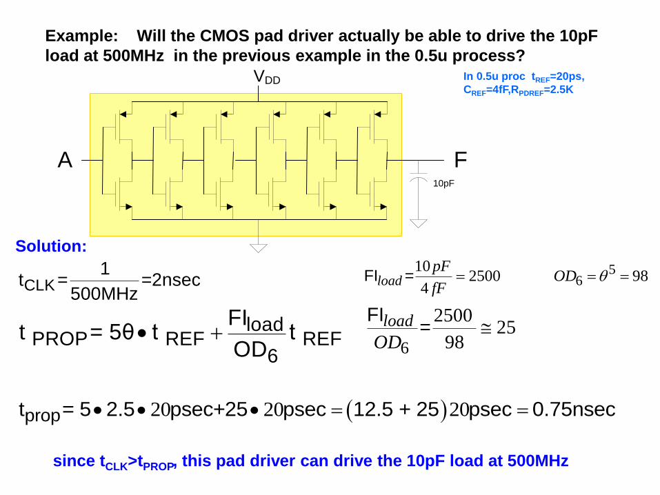
A F
VDD
10pF
Example: Will the CMOS pad driver actually be able to drive the 10pF
load at 500MHz in the previous example in the 0.5u process?
Solution:
In 0.5u proc tREF=20ps,
CREF=4fF,RPDREF=2.5K
loadPROP REF REF
6
FIt = 5θ t t
OD
20 20 20propt = 5 2.5 psec+25 psec 12.5 + 25 psec 0.75nsec
CLK1
t = =2nsec500MHz
since tCLK>tPROP, this pad driver can drive the 10pF load at 500MHz
56
102500 98
4FI = load
pFOD
fF
6
250025
98
FI= load
OD

A F
VDD
10pF
Example: Determine the dynamic power dissipation in the next to the
last stage of a 6-stage CMOS pad driver if used to drive a 10pF
capacitive load if clocked at 500MHz. Assume pad driver with OD of
θ=2.5 and VDD=3.5V
Solution:
In 0.5u proc tREF=20ps,
CREF=4fF,RPDREF=2.5K
2DYN CL L DD
P =f C V 2.42=5E8 390fF 3.5 mW
CIN
5IN REFC =θ C 5=2.5 4fF=390fF

A F
VDD
10pF
Example: Is the 6-stage CMOS pad driver adequate to drive the 10pF
capacitive load as fast as possible? Assume pad driver with OD of
θ=2.5 and VDD=3.5V
Solution:
In 0.5u proc tREF=20ps,
CREF=4fF,RPDREF=2.5K
7.8LOPT
REF
C 10pFn ln ln
C 4fF
No – an 8-stage pad driver would drive the load much faster (but is not needed
If clocked at only 500MHz)

Example: Determine the power that would be required in the last
stage of a CMOS pad driver to drive a 32-bit data bus off-chip if the
capacitive load on each line is 2pF. Assume the clock speed is 500MHz
and that each bit has an average 50% toggle rate. Assume VDD=3.5V
Solution:
In 0.5u proc tREF=20ps,
CREF=4fF,RPDREF=2.5K
2CLDYN L DD
fP =32 C V
2 25E8
=32 2pF 3.5 196mW2
Note: A very large amount of power is required to take a large bus off-chip
if bus has a high rate of activity.
Digital Circuit Design
• Hierarchical Design
• Basic Logic Gates
• Properties of Logic Families
• Characterization of CMOS
Inverter
• Static CMOS Logic Gates
– Ratio Logic
• Propagation Delay
– Simple analytical models• FI/OD
• Logical Effort
– Elmore Delay
• Sizing of Gates
• Propagation Delay with
Multiple Levels of Logic
• Optimal driving of Large
Capacitive Loads
• Power Dissipation in Logic
Circuits
• Other Logic Styles
• Array Logic
• Ring Oscillators
done
partial

Logic Styles
• Static CMOS
• Complex Logic Gates
• Pass Transistor Logic (PTL)
• Pseudo NMOS
• Dynamic Logic
– Domino
– Zipper

Complex Logic GatesVDD
AB
PUN
PDN
n
• Implement B in PDN
• Implement B in PUN with complimented input variables
p-channel
n-channel
• Zero static power dissipation
• VH=VDD, VL=0V (or VSS)
• Complimented input variables often required
Have implemented the logical function twice (once in PU, again in PD)
and this is a major contributor to increased area and dynamic power
dissipation

• Low device count implementation of non inverting function (can be dramatic)
• Logic Swing not rail to rail
• Static power dissipation not 0 when F high
• RLG may be unacceptably large
• Slow tLH
• Signal degradation can occur when multiple levels of logic are used
• Widely used in some applications
• Implements basic logic function only once!
VDD
A B
F
RLG
F=A•B
Pass Transistor Logic
Observations about PTL

Pseudo NMOS Logic
n could be several hundred or even several thousand
F
A1A2 An
VDD

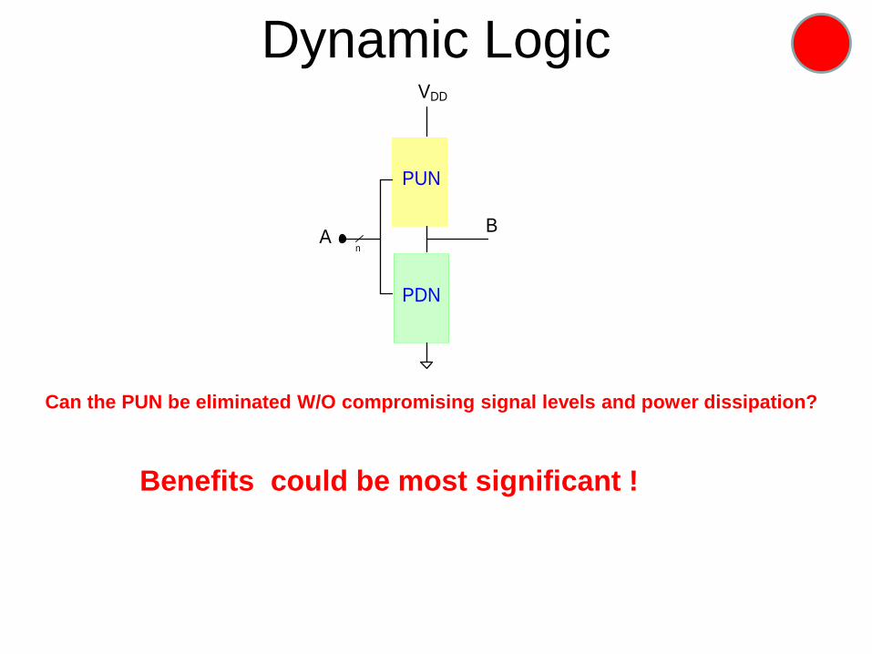
Dynamic Logic
VDD
AB
PUN
PDN
n
• PTL reduced complexity of either PUN or PDN to single “resistor”
• PTL relaxed requirement of all n-channel or all p-channel devices in
PUN/PDN
What is the biggest contributor to area?
What is biggest contributor to dynamic power dissipation ?
PUN (3X active area for inverter, more for NOR
gates, and Well)
PUN and is responsible for approximately 75% of the dynamic power
dissipation in inverter, more in NOR gates !
Can the PUN be eliminated W/O compromising signal levels and power dissipation?
Dynamic LogicVDD
AB
PUN
PDN
n
Can the PUN be eliminated W/O compromising signal levels and power dissipation?
Benefits could be most significant !
Dynamic Logic
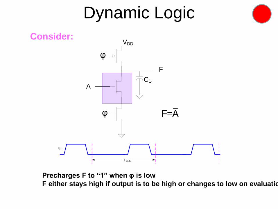
TCLK
φ
VDD
F
φ
CD
A
F=A
φ
Precharges F to “1” when φ is low
F either stays high if output is to be high or changes to low on evaluation
Consider:

Dynamic LogicVDD
F
φ
CD
A
F=A
φ
VDD
F
φ
CD
A
F=A B
B
φ
F
φ
CD
A
F=A B
B
φ
VDD
• Termed Dynamic Logic Gates
• Parasitic capacitors actually replace CD
• If Logic Block is n-channel, will have rail to rail
swings
• Logic Block is simply a PDN that implements F
TCLK
φ
Consider:
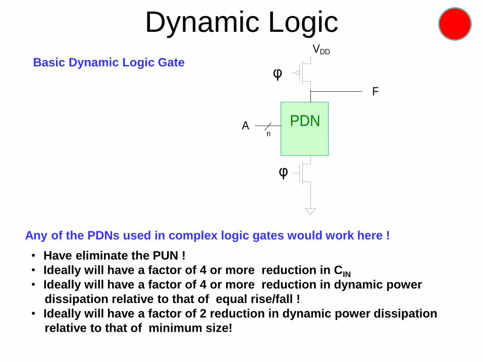
Dynamic LogicVDD
F
φ
A PDNn
φBasic Dynamic Logic Gate
Any of the PDNs used in complex logic gates would work here !
• Have eliminate the PUN !
• Ideally will have a factor of 4 or more reduction in CIN
• Ideally will have a factor of 4 or more reduction in dynamic power
dissipation relative to that of equal rise/fall !
• Ideally will have a factor of 2 reduction in dynamic power dissipation
relative to that of minimum size!

From Wikipedia: Apr 23 2018

Dynamic LogicVDD
F
φ
A PDNn
φ
Basic Dynamic Logic Gate
Advantages:
•Lower dynamic power dissipation (Ideally 4X)
• Improved speed (ideally 4X)Limitations:
• Output only valid during evaluate state
• Need to route a clock
(and this dissipates some power)
• Premature Discharge !
• More complicated
• Charge storage on internal nodes of PDN
• No Static hold if output H

Dynamic Logic
Premature Discharge Problem
If A is high, then F may go low at the start of the evaluate cycle and there
is no way to recover a high output later in the evaluate phase - i.e. there may
be a boolean error!.
Can not reliably cascade dynamic logic gates !
VDD
F
φ
A
VDD
φ
φφ

Dynamic Logic
Premature Discharge Problem
This problem occurs when any inputs to an arbitrary dynamic logic gate
create an RPD path in the PDN during at the start of the evaluate phase
that is not to pull down later in that evaluate phase
VDD
φ
A PDNn
VDD
φ
PDNn
Fφφ
Precharging to the low level all inputs to a PDN that may change to the
high state later in the evaluate cycle (called domino)
How can this problem be fixed?
Alternating gates with n-channel and p-channel pull networks
(Zipper Logic)

Dynamic Logic
Premature Discharge Problem
VDD
φ
A PDNn
Fφ
VDD
φ
A PDNn
F
VDD
φ
Some additional dynamic power dissipation in the inverter
Some additional delay during the evaluate state in inverter
Adding an inverter at the output will cause F to precharge low so it can
serve as input to subsequent gate w/o causing premature discharge
Implement F instead of in the PDN F
Termed Domino Logic
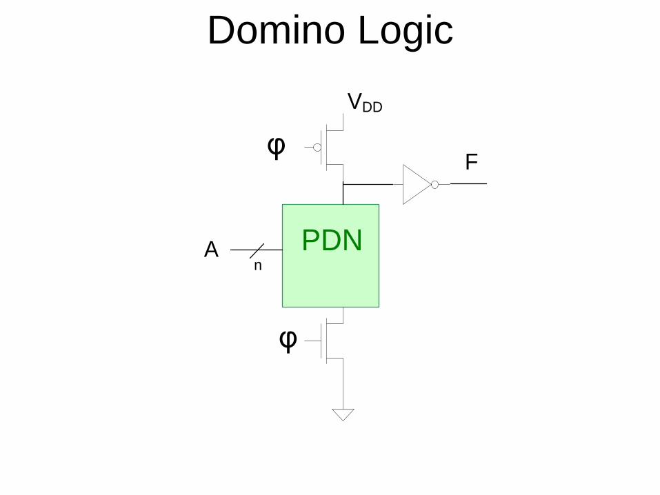
Domino Logic
VDD
φ
A PDNn
Fφ

Dynamic Logic
• p-channel logic gate will pre-charge low
• Phasing of PUN and PDN networks is reversed
• Some performance loss with p-channel logic devices
• Direct coupling between alternate type dynamic gates is possible
without causing a premature discharge problem
VDD
F
φ
A PDNn
VDD
F
A PUNn
φ
φ
φ

Dynamic Logic
Direct coupling between alternate type dynamic gates
VDD
φ
φ
A PDNn
VDD
F
φ
φ
PUN

Zipper Logic
Map gates to appropriate precharge type

Zipper Logic
Acceptable Implementation in Zipper
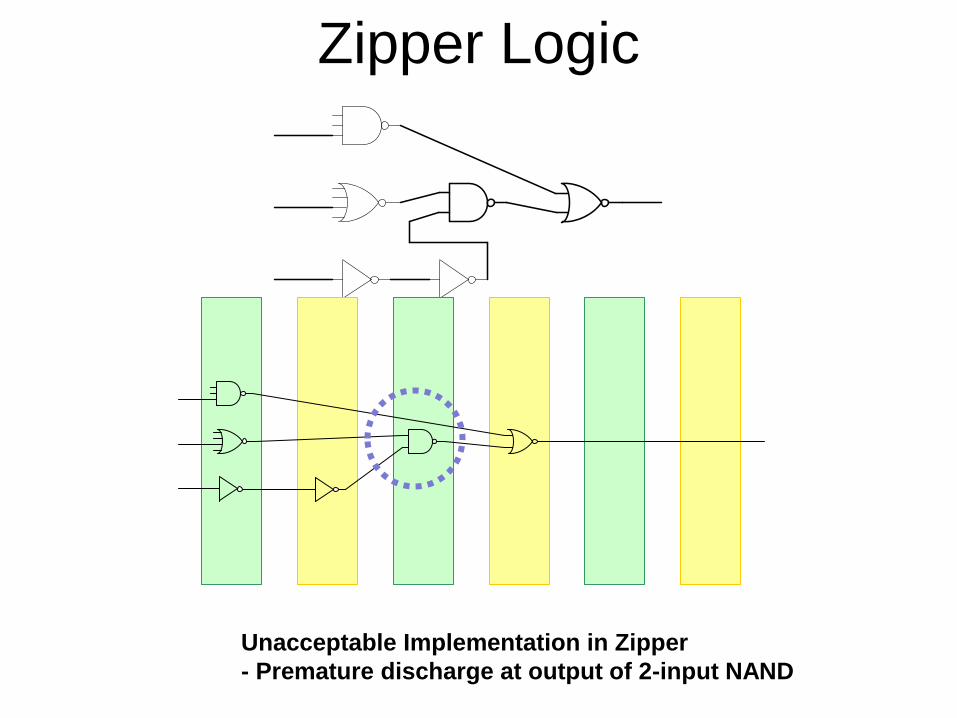
Zipper Logic
Unacceptable Implementation in Zipper
- Premature discharge at output of 2-input NAND

Zipper Logic
Another acceptable Implementation in Zipper
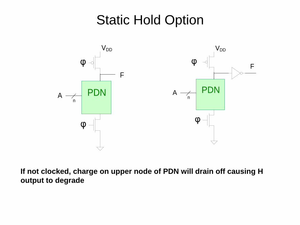
Static Hold Option
VDD
φ
A PDNn
Fφ
VDD
φ
A PDNn
F
φ
If not clocked, charge on upper node of PDN will drain off causing H
output to degrade
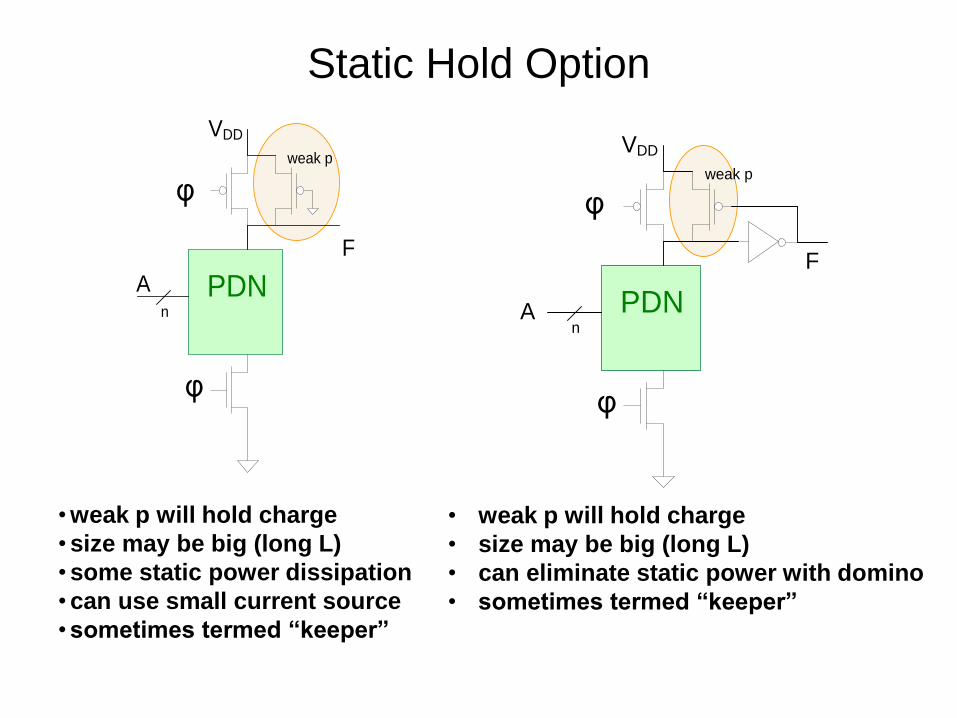
Static Hold Option
• weak p will hold charge
• size may be big (long L)
• can eliminate static power with domino
• sometimes termed “keeper”
VDD
φ
A PDNn
F
weak p
φ
VDD
φ
A PDNn
F
weak p
φ
•weak p will hold charge
•size may be big (long L)
•some static power dissipation
•can use small current source
•sometimes termed “keeper”
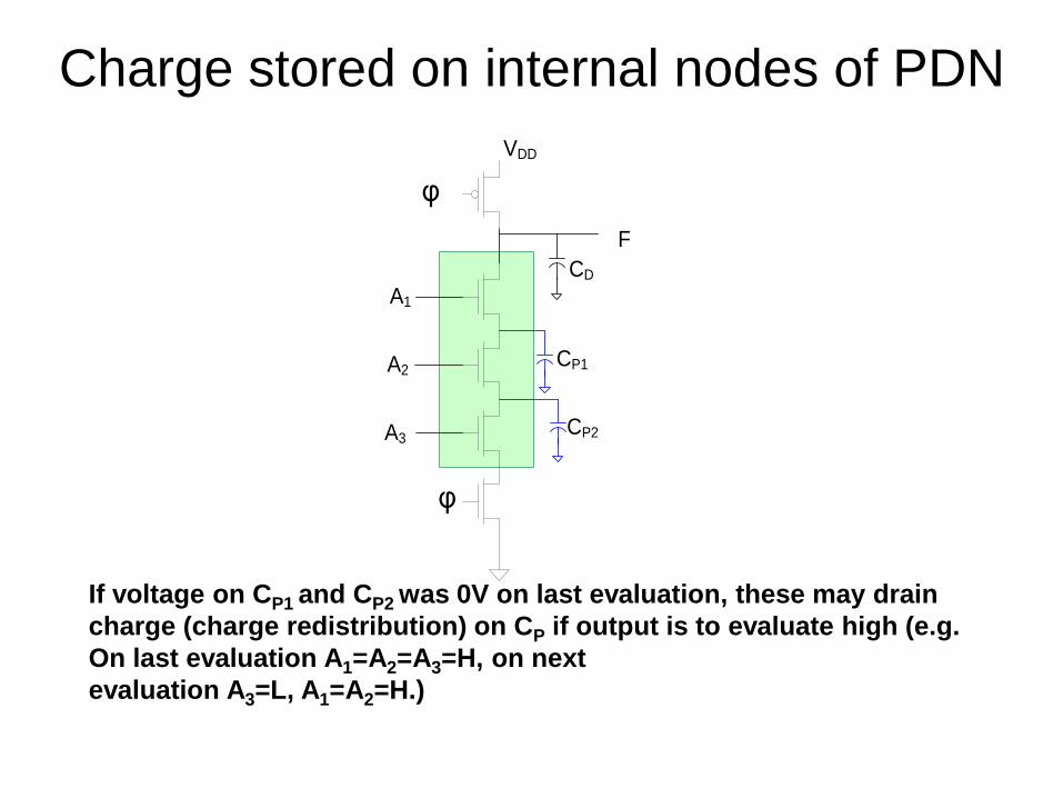
Charge stored on internal nodes of PDN
VDD
F
φ
CD
A1
A2
A3
CP1
CP2
φ
If voltage on CP1 and CP2 was 0V on last evaluation, these may drain
charge (charge redistribution) on CP if output is to evaluate high (e.g.
On last evaluation A1=A2=A3=H, on next
evaluation A3=L, A1=A2=H.)

Charge stored on internal nodes of PDN
VDD
F
φ
CD
A1
A2
A3
CP1
CP2
φ
Can precahrge internal nodes to eliminate undesired charge redistribution
VDD
F
φ
CDA1
A2
A3
CP1
CP2
φ
Dynamic Logic
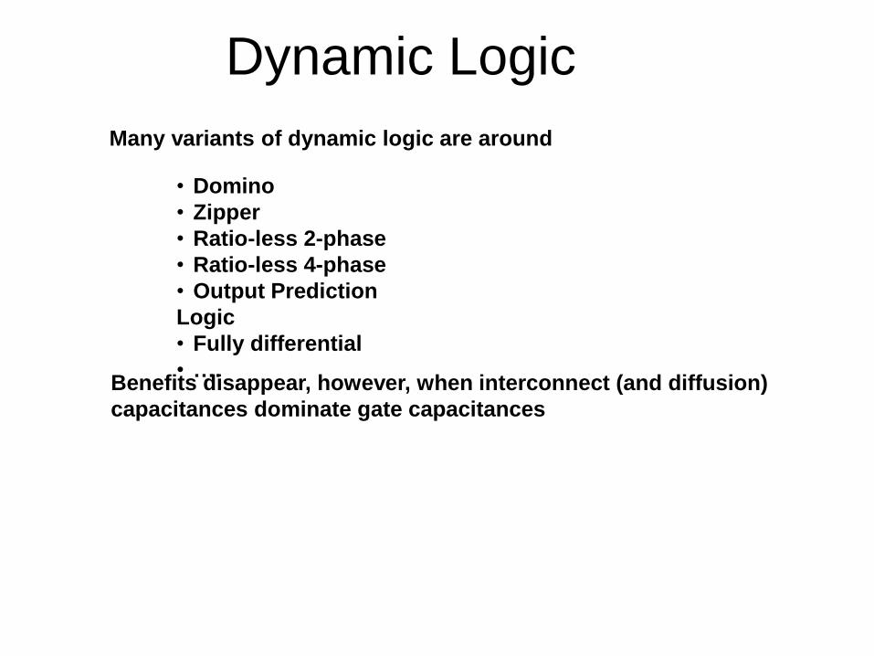
Many variants of dynamic logic are around
• Domino
• Zipper
• Ratio-less 2-phase
• Ratio-less 4-phase
• Output Prediction
Logic
• Fully differential
• ….Benefits disappear, however, when interconnect (and diffusion)
capacitances dominate gate capacitances
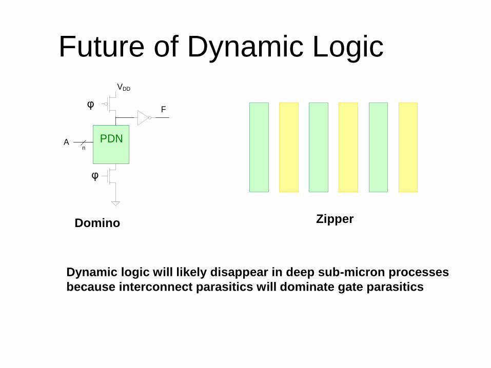
Future of Dynamic LogicVDD
φ
A PDNn
Fφ
Dynamic logic will likely disappear in deep sub-micron processes
because interconnect parasitics will dominate gate parasitics
Domino Zipper
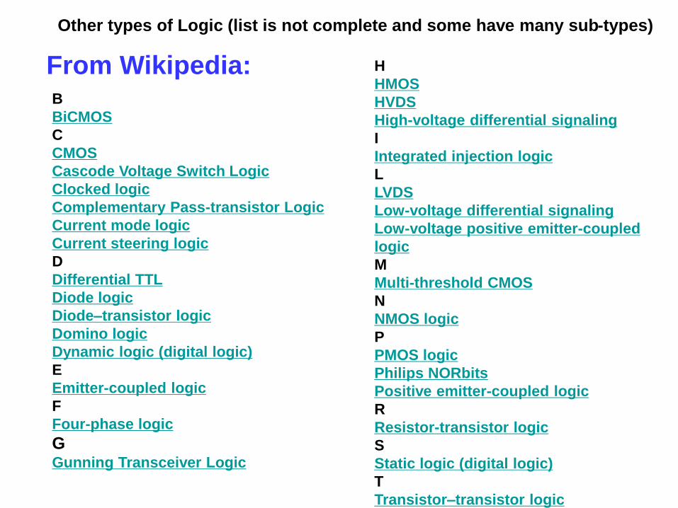
From Wikipedia:B
BiCMOS
C
CMOS
Cascode Voltage Switch Logic
Clocked logic
Complementary Pass-transistor Logic
Current mode logic
Current steering logic
D
Differential TTL
Diode logic
Diode–transistor logic
Domino logic
Dynamic logic (digital logic)
E
Emitter-coupled logic
F
Four-phase logic
GGunning Transceiver Logic
H
HMOS
HVDS
High-voltage differential signaling
I
Integrated injection logic
L
LVDS
Low-voltage differential signaling
Low-voltage positive emitter-coupled
logic
M
Multi-threshold CMOS
N
NMOS logic
P
PMOS logic
Philips NORbits
Positive emitter-coupled logic
R
Resistor-transistor logic
S
Static logic (digital logic)
T
Transistor–transistor logic
Other types of Logic (list is not complete and some have many sub-types)

End of Lecture 43