dielectricity the phenomena of formation of dipole is...
TRANSCRIPT

DielectricityDielectricity
Dielectric materials: Materials which is generally insulators. Under applied electric field, there is a tiny movement of charge inside the material.
� Creation of DIPOLE (two poles)Electricfield
The phenomena of formation of dipole is called Polarization
Polarization can occur in 4 ways
1. Electronic PolarizationCloud of electrons moves in direction of electric field.
2. Orientation PolarizationDipole molecule (HCl, H2O, HF, etc) moves in direction of electric field
3. Space Charge PolarizationAccumulation of charge in some area of material.
4. Atomic หรือ Ionic PolarizationDistortion or change of position of ion in crystal structure.
(Analogous to magnetization of magnetic dipole)
(in polar molecule, H+2O
-)
(movement of charged particles in direction of electric field)
(distortion of crystal structure by the small displacement of the ion in direction of electric field)
ElectrodeDielectric
Electrode
Mobile chargeFixed charge
E
Accumulated charge
E
Grain boundary or interface
(c)
(a) (b)
Space Charge Polarization (a) no electric field (b) positive ion has high mobility (c) accumulation at grain boundary, phase boundary, or defects.
(the ions which are more mobile will move to available space inside the solid, such as grain boundaries, and other defects)

p+ p–
x
p'+ p'–
E
Cl– Na+
(a)
(b)
Fig. 7.8: (a) A NaCl chain in the NaCl crystal without anapplied field. Average or net dipole moment per ion is zero.(b) In the presence of an applied field the ions becomeslightly displaced which leads to a net average dipolemoment per ion.
Ionic polarizationElectric field: volt per meter.Electric field: volt per meter. The voltage of the electrodes divided by distance between the electrodes. The larger the voltage or the nearer the two electrodes, the stronger the electric field.
Capacitance (C)Capacitance (C)
C = Q/V farad = coulomb/voltCapacitance = amount of accumulated charge under 1 V applied voltage.
V
Q is amount of charge that is accumulated inside the materials
Voltage from battery
Dielectric Constant Dielectric Constant is a material property, showing the capacity of a material to accumulate charges, under applied electric field.
C = εA / l farad = (farad/cm)(cm2)/(cm)• Capacitance depends on size (A), distance between plates (l) , and materials in the middle.
• value of ε is a property of material called ‘Permittivity’• ε of vacuum = ε0 = 8.85x10⁻¹⁴ farad/cm• ε’ = ε/ε0 = relative permittivity = dielectric constant• some textbooks use K’ and K instead of ε’ and ε
C = ε’ε0(A/l)Analogous to B = µrµ0H in magnetism.

To increase C, one can increase ε, A, and decrease l. Increase ε by selection of proper dielectric materials with high ε’ valueIncrease A by using multilayer configuration
Which one will be your selection?
Dielectric constant depends onfrequency of the electric field (how fast the switching of + and – electrode)
The charge movement inside the materials cannot keep up with the changing of the charge of the electrodes
Effect of frequency to dielectric constant at constant temperature
1 102 104 106 108 1010 1012 1014 101610-2
ƒ
Orientational,Dipolar
Interfacial andspace charge
IonicElectronic
εr'
εr''
Radio Ultraviolet lightInfrared
εr' = 1
From Principles of Electronic Materials and Devices, Second Edition, S.O. Kasap (© McGraw-Hill, 2002)http://Materials.Usask.Ca
Fig. 7.14: The frequency dependence of the real and imaginary partsof the dielectric constant in the presence of interfacial, orientational,ionic and electronic polarization mechanisms.
Diele
ctric
cons
tant
Frequency
Why does the decrease is in steps ?

Effect of temperature to dielectric constant at constant frequency Effect of both frequency and temperature to dielectric constant
Effect of both frequency and temperature to dielectric constant Dielectric StrengthMaximum voltage that can be applied per thickness of material.
Unit is V/mil or V/cm(mil = 0.001 inch)
Keep in mind that short circuit will occur at large voltage.

Dielectric LossAmount of energy loss from movement of ions under applied alternate voltage.
Why these materials have high dielectric constant?
Movement of large positive charge (Ti4+) inside the unit cell of perovskite structure

Cubic (Perovskite) – random orientation of Ti4+ – random polarizationTetragonal– Ti4+ move to near O2- at face center – permanent dipole Phase transformation Cubic � Tetragonal is called Curie temperature
Doping will change the shape of the graph and position of maximum K’BaTiO3+CaZrO3+MgZrO3 – broadening of peak BaTiO3+PbTiO3 – increase curie temperatureBaTiO3+SrTiO3+SrSnO3+CaSnO3+BaSnO3 – decrease curie temperature
read Strontium stannate

1 pF 1 nF 1 µF 1 mF
Capacitance
Paper and Plastic Film
Electrolytic Al, Ta
Solid Electrolytic Al, Ta
Mica Film
Single Layer Ceramic
Multilayer Ceramic
From Principles of Electronic Materials and Devices, Second Edition, S.O. Kasap (© McGraw-Hill, 2002)http://Materials.Usask.Ca
Fig. 7.27: Examples of dielectrics that can be used for variouscapacitance values.
1 Hz 1 kHz 1 MHzFrequency
1 GHz
Ta Electrolytic
Al Electrolytic
Polymer Film
Mica Film
Low-loss ceramic and glass
High Permittivity Ceramic
From Principles of Electronic Materials and Devices, Second Edition, S.O. Kasap (© McGraw-Hill, 2002)http://Materials.Usask.Ca
Fig. 7.28: Examples of dielectrics that can be used in various requencyranges.
From Principles of Electronic Materials and Devices, Second Edition, S.O. Kasap (© McGraw-Hill, 2002)http://Materials.Usask.Ca
(b) Multilayer ceramic capacitor(stacked ceramic layers)
Metal termination
Metal electrode
CeramicEpoxy
Leads
(a) Single layer ceramic capacitor(e.g. disk capacitors)
Fig. 7.29: Single and multilayer dielectric capacitors
Al metallizationPolymer film
(a)
(b)
Fig. 7.30 Two polymer tapes in (a) each with a metallized film electrodeon the surface (offset from each other) can be rolled together (like aSwiss roll-cake) to obtain a polymer film capacitor as in (b). As the twoseparate metal films are lined at oppose edges, electroding is done overthe whole side surface.From Principles of Electronic Materials and Devices, Second Edition, S.O. Kasap (© McGraw-Hill, 2002)http://Materials.Usask.Ca

(a)
Al foils
Al case
Al2O3Anode Cathode
(b)
Electrolyte
Al Al
Fig. 7.31: Al electrolytic capacitor.
From Principles of Electronic Materials and Devices, Second Edition, S.O. Kasap (© McGraw-Hill, 2002)http://Materials.Usask.Ca
Electrolyte: Sodium Borate
Ta
Ta2O5
MnO2
Graphite
Silver paste
(b)
Epoxy Silver paint
Lads
Ta
(a)
From Principles of Electronic Materials and Devices, Second Edition, S.O. Kasap (© McGraw-Hill, 2002)http://Materials.Usask.Ca
Fig. 7.32: Solid electrolyte tantalum capacitor. (a) A cross sectionwithout fine detail. (b) An enlarged section through the Tacapacitor.
Piezoelectricity: PressurePiezoelectricity: Pressure���������������� ElectricityElectricity
• When material is under stress, it generates Dipole in the material.• Amount of Dipole is linearly proportional of applied stress.• On the other hand, when applying voltage, it generate stress in the material, and may cause change of shape of material.• Application: ultrasonic device, microphone, phonograph cartridge, accelerometer, strain gauges, sonar devices, actuator
• With appropriate applied force in a direction, it will generate Dipole in the unit cell of Piezoelectric ceramic, causing voltage in the material.• On the other hand, applied voltage causing distortion of unit cell.

Unit cell without Center Symmetry has Piezoelectric property, under applied force in an appropriate direction.Ex: Quartz (a crystal structure of SiO2) in direction [100] cause Polarization but direction [001] does not cause Polarization: Your homework!
Fig. Edison cylinder phonograph: 1899
Source:http://en.wikipedia.org/wiki/Phonograph
Air pressure from wave of sound is store as roughness on the surface of the wax.
Roughness causes vibration at stylus (pen) and causes stress to the piezoelectric ceramic.
Voltage signal from amplifier cause contraction and expansion of the piezoelectric ceramic.
That causes vibration of the diaphragmof the speaker of the headphone.

Hydrophone is a device for listening to sound under water.
Accelerometer is a device for measuring mass movement or acceleration.
Fig. 7.38: Piezoelectric transducers are widely used to generateultrasonic waves in solids and also to detect such mechanicalwaves. The transducer on the left is excited from an ac sourceand vibrates mechanically. These vibrations are coupled to thesolid and generate elastic waves. When the waves reach theother end they mechanically vibrate the transducer on the rightwhich converts the vibrations to an electrical signal.
Oscillator
Elasticwaves in thesolid Oscilloscope
A B
Mechanicalvibrations
Piezoelectrictransducer
From Principles of Electronic Materials and Devices, Second Edition, S.O. Kasap (© McGraw-Hill, 2002)http://Materials.Usask.Ca
Piezoelectric detector
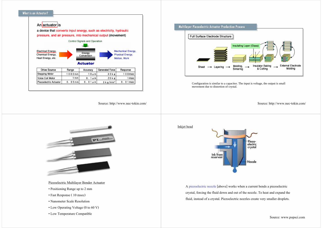
Source: http://www.nec-tokin.com/ Source: http://www.nec-tokin.com/
Configuration is similar to a capacitor. The input is voltage, the output is small movement due to distortion of crystal.
Piezoelectric Multilayer Bender Actuator• Positioning Range up to 2 mm • Fast Response ( 10 msec) • Nanometer Scale Resolution • Low Operating Voltage (0 to 60 V) • Low Temperature Compatible
A piezoelectric nozzle [above] works when a current bends a piezoelectric crystal, forcing the fluid down and out of the nozzle. To heat and expand the fluid, instead of a crystal. Piezoelectric nozzles create very smaller droplets.
Source: www.popsci.com
Inkjet head

Some of the common applications for piezoelectric motors includes camera focus systems, computer disk drives, material handling, robotics, and semiconductor testing and production systems.
Driven by dual orthogonal vibration modes with a phase shift of 90°, the contact point between two surfaces vibrates in an elliptical path, producing a frictional force between the surfaces. Usually, one surface is fixed causing the other to move. In most piezoelectric motors the piezoelectric crystal is excited by a sine wavesignal at the resonant frequency of the motor. Using the resonance effect, a much lower voltage can be used to produce a high vibration amplitude.
PyroelectricityPyroelectricity:: Fire + Electricity
• It is a subclass of Piezoelectricity• Under heat, material is distorted and expanded, causing formation of Dipole, and generate voltage in the material.• Ex: Wurtzite (hexagonal ZnS), Tourmaline, Rochelle salt, Triglycine salfate, BaTiO3, Pb(Zr,Ti)O3, Lithium sulfate, LiTaO3
• Usage: measuring of temperature at high sensitivity: 10-6 oC
1: Single crystal LiTaO3
2&3: Electrodeu0: output voltage
RF: radiant flux (heat)
1
2
3
RF
u0
FerroelectricityFerroelectricity
• It is a Subclass of Pyroelectricity• It has Hysteresis loop which is change of Polarization under applied voltage.
P = Polarization: µC/cm2
E = Electric field: V/cm
Ps – Spontaneous polarizationPr – Remanent polarizationB – SaturationEc – Coercive field
p+ p–
x
p'+ p'–
E
Cl– Na+
(a)
(b)
Fig. 7.8: (a) A NaCl chain in the NaCl crystal without anapplied field. Average or net dipole moment per ion is zero.(b) In the presence of an applied field the ions becomeslightly displaced which leads to a net average dipolemoment per ion.

Area = A ptotal
P-QP +QP
d
(c)
+Q E -Q
V(a)
-QP +QP
Bound polarizationcharges on the surfaces
(b)
From Principles of Electronic Materials and Devices, Second Edition, S.O. Kasap (© McGraw-Hill, 2002)http://Materials.Usask.Ca
Fig. 7.4: (a) When a dilectric is placed in an electric field, boundpolarization charges appear on the opposite surfaces. (b) The originof these polarization charges is the polarization of the molecules ofthe medium. (c) We can represent the whole dielectric in terms of itssurface polarization charges +QP and -QP.
P = ptotal/ volume= (Qp d) / (A d)= Qp/A= coulomb/m2
Domain – บริเวณทีZมีทิศทางของ Dipole ไปในทางเดียวกนั