diffusion in gaaspearton.mse.ufl.edu/semic_properties/data/5032.pdf · notes: each item in this...
TRANSCRIPT

SCITEC PUBLICATIONS
Diffusion in GaAsand other III-V Semiconductors10 Years of Research
Editor:
D.J. Fisher

Notes:Each item in this section of the volume begins with a graphical compilation of relevant diffusion data whichhave been reported during the past decade. The plotted data are also tabulated as indicated on the graph. In somecases, the tabulated data have been obtained by digitizing published graphs and the values may not correspondexactly with the author's unpublished raw data.
3N Bulk Diffusion - Quantitative DataThe migration of Ag from epitaxial layers and into (111) samples of Si,during annealing at temperatures of between 450 and 500C, was studiedby means of secondary ion mass spectrometric depth profiling. It wasfound that the diffusivities lay between 8 x 10 -16 and 1.6 x 10⁻¹⁵cm2/s(table N). These values were lower than were expected on the basis ofprevious data.T.C.Nason, G.R.Yang, K.H.Park, T.M.Lu: Journal of Applied Physics,1991, 70[3], 1392-6
[446-91/92-027]
Refers to table N
Indicates volume and page number inDDF where abstract first appeared
227
AlAs
Ag
AlAs/GaAs: Ag DiffusionVarious elements were diffused into a superlattice structure at temperatures of between700 and 1000C. Their disordering effect upon the superlattice was assessed by using asmall-angle polishing method. The diffusion of Ag had no disordering effect upon thesuperlattice. The results were explained in terms of the interstitial-substitutionalmechanism, and of the solubility of the given dopant in GaAs.H.P.Ho, I.Harrison, N.Baba-Ali, B.Tuck, M.Henini: Journal of Electronic Materials,1991, 20[9], 649-52
[446-84/85-002]
Al
31 AlAs/GaAs: Al DiffusionThe intermixing of superlattices was investigated as a function of the Si concentrationfollowing annealing at temperatures ranging from 500 to 900C. The superlattice sampleswere prepared by means of molecular beam epitaxy, and the near-surface layers weredoped with Si to concentrations of between 2 x 10¹⁷ and 5 x 10¹⁸/cm3. The Si and Aldepth profiles were measured by means of secondary ion mass spectrometry. Thediffusion length and activation energy of Al, as a function of Si dopant concentration,were deduced from the secondary ion mass spectrometry data. Within the abovetemperature range a single activation energy, for Al diffusion, of about 4eV was observed(table 1). The Al diffusion coefficient increased rapidly with Si concentration.P.Mei, H.W.Yoon, T.Venkatesan, S.A.Schwarz, J.P.Harbison: Applied Physics Letters,1987, 50[25], 1823-5
[446-157/159-227]

228
Al AlAs Au
Table 1Diffusivity of Al in AlAs/GaAs
Si (/cm3) Temperature (C) D (cm2/s)5 x 1017 900 6.1 x 10⁻¹⁷
5 x 10¹⁷ 850 3.0 x 10⁻¹⁷
1 x 10¹⁸ 795 5.0 x 10⁻¹⁷
2 x 10¹⁸ 750 6.6 x 10⁻¹⁷
2 x 10¹⁸ 750 5.4 x 10⁻¹⁷
5 x 10¹⁸ 700 4.2 x 10⁻¹⁷
5 x 10¹⁷ 795 2.3 x 10⁻¹⁸
2 x 10¹⁸ 695 1.1 x 10⁻¹⁷
2 x 10¹⁸ 700 5.6 x 10⁻¹⁸
5 x 10¹⁸ 650 5.6 x 10⁻¹⁸
1 x 10¹⁸ 745 2.6 x 10⁻¹⁸
2 x 10¹⁸ 655 1.0 x 10⁻¹⁸
2 x 10¹⁸ 655 7.3 x 10⁻¹⁹
2 x 10¹⁷ 900 1.2 x 10⁻¹⁷
5 x 10¹⁷ 745 3.6 x 10⁻¹⁹
- 850 4.2 x 10⁻²⁰
- 800 2.6 x 10⁻²⁰
AlAs/GaAs: Al DiffusionEnhanced layer interdiffusion. in Te-doped (2 x 10¹⁷ to 3 x 10¹⁸/cm3) organometallicchemical vapor deposited superlattices was studied by using secondary ion massspectrometry. It was found that, at temperatures ranging from 800 to 1000C, the Aldiffusion coefficient had an activation energy of 3eV and was approximately proportionalto the Te content. In the case of Si-induced mixing, the activation energy for Al diffusionwas 4.1eV and exhibited a power-law dependence upon the Si content.P.Mei, S.A.Schwarz, T.Venkatesan, C.L.Schwartz, E.Colas: Journal of Applied Physics,1989, 65[5], 2165-7
[446-72/73-002]
Au
AlAs/GaAs: Au DiffusionVarious elements were diffused into a superlattice structure at temperatures of between700 and 1000C. Their disordering effect upon the superlattice was assessed by using asmall-angle polishing method. The diffusion of Au had no disordering effect upon the

229
Au AlAs Si
superlattice. The results were explained in terms of the interstitial-substitutionalmechanism, and of the solubility of the given dopant in GaAs.H.P.Ho, I.Harrison, N.Baba-Ali, B.Tuck, M.Henini: Journal of Electronic Materials,1991, 20[9], 649-52
[446-84/85-002]
Cu
AlAs/GaAs: Cu DiffusionVarious elements were diffused into a superlattice structure at temperatures of between700 and 1000C. Their disordering effect upon the superlattice was assessed by using asmall-angle polishing method. The diffusion of Cu had no disordering effect upon thesuperlattice. The results were explained in terms of the interstitial-substitutionalmechanism, and of the solubility of the given dopant in GaAs.H.P.Ho, I.Harrison, N.Baba-Ali, B.Tuck, M.Henini: Journal of Electronic Materials,1991, 20[9], 649-52
[446-84/85-002]
Mn
AlAs/GaAs: Mn DiffusionVarious elements were diffused into a superlattice structure at temperatures of between700 and 1000C. Their disordering effect upon the superlattice was assessed by using asmall-angle polishing method. It was found that Mn induced disordering of thesuperlattice. However, the disordering effect which arose from Mn diffusion could beentirely inhibited if the fraction of As in the diffusion source were considerably higherthan that of Mn. This inhibition effect was related to the formation of MnAs or MnAs2.This left very little Mn, in the vapor phase, which was available for diffusion. The resultswere explained in terms of the interstitial-substitutional mechanism, and of the solubilityof the given dopant in GaAs.H.P.Ho, I.Harrison, N.Baba-Ali, B.Tuck, M.Henini: Journal of Electronic Materials,1991, 20[9], 649-52
[446-84/85-002]
Si
AlAs/AlGaAsP/GaAs: Si DiffusionThe diffusion of SiIII-SiV neutral pairs versus the diffusion of SiIII-VIII complexes in III-Vcrystals was considered with regard to experimental data which revealed the effect of Sidiffusion upon the self-diffusion of column-III and column-V lattice atoms. Secondaryion mass spectroscopy was used to compare the enhanced diffusion of column-III orcolumn-V atoms in various Si-diffused heterostructures which were closely lattice-
230
Si AlAs Surface
matched to GaAs. An enhancement of lattice atom self-diffusion, due to impuritydiffusion, was found to occur predominantly on the column-III lattice. The data supportedthe SiIII-VIII diffusion model and indicated that the main native defects whichaccompanied Si diffusion were column-III vacancies. These diffused directly on thecolumn-III sub-lattice.D.G.Deppe, W.E.Plano, J.E.Baker, N.Holonyak, M.J.Ludowise, C.P.Kuo, R.M.Fletcher,T.D.Osentowski, M.G.Craford: Applied Physics Letters, 1988, 53[22], 2211-3
[446-64/65-157]
Zn
AlAs/GaAs: Zn DiffusionThe diffusion of Zn into superlattices was studied by using transmission electronmicroscopy and secondary ion mass spectroscopy. It was found that micro-defects existednear to the Zn diffusion front. These defects were interstitial dislocation loops. It wassuggested that the diffusion of Zn into the present materials was similar to Zn diffusioninto GaAs. This was considered to be evidence for an interstitial mechanism for theenhancement of interdiffusion.I.Harrison, H.P.Ho, B.Tuck, M.Henini, O.H.Hughes: Semiconductor Science andTechnology, 1989, 4[10], 841-6
[446-72/73-002]
AlAs/GaAs: Zn DiffusionThe effect of an As pressure upon the disordering effect of Zn diffusion into superlatticeswas studied. It was found that the degree of disordering increased when no excess As wasadded to the ampoule. It had previously been found that dislocation loops formed near tothe Zn diffusion front. The same effect was observed here, except when Zn diffusion wascarried out in the absence of excess As. The Zn penetration was found to be greatestwhen no excess As was added to the diffusion ampoule.I.Harrison, H.P.Ho, B.Tuck, M.Henini, O.H.Hughes: Semiconductor Science andTechnology, 1990, 5[6], 561-5
[446-74-001]
Surface Diffusion
Al
AlAs: Al Surface DiffusionDuring the molecular beam epitaxial growth of AlAs on the vicinal (100) surface ofGaAs, reflection high-energy electron diffraction was used to measure the transitiontemperature between 2-dimensional nucleation and pure step propagation which occurredwhen sub-monolayer amounts of Sn were present on the surface. In the case of samples

231
Surface AlAs Surface
which were misoriented by 0.5º with respect to the [011] or [011] direction, the transitiontemperature decreased by approximately 100C after the deposition of 0.6 of a monolayerof Sn. The presence of Sn increased the surface mobility of Al adatoms on (100) AlAssurfaces; as indicated by the annealing behavior of the AlAs surface at 600C.G.S.Petrich, A.M.Dabiran, P.I.Cohen: Applied Physics Letters, 1992, 61[2], 162-4
[446-93/94-001]
AlAs/GaAs: Al Surface DiffusionA study was made of reflection high-energy electron diffraction specular-beam intensityoscillations on vicinal (001)AlAs which had been grown onto GaAs(001) substrates thatwere misoriented by 2 or 3° towards [110], [010], or [110]. It was found that thetemperature dependence of the oscillation behavior on vicinal surfaces was similar to thaton GaAs(001) and InAs(001). Contrary to the case of GaAs(001), however, the surfacereconstruction could not be kept constant during the growth-mode transition and it wastherefore difficult to analyze AlAs(001) data in as much detail as that for GaAs(001).Nevertheless, from the similarity between them it was estimated that the effective surfacemigration barrier for Al adatoms on AlAs(001) was about 1.74eV.T.Shitara, J.H.Neave, B.A.Joyce: Applied Physics Letters, 1993, 62[14], 1658-60
[446-106/107-007]
Ga
AlAs: Ga Surface DiffusionDuring the molecular beam epitaxial growth of AlAs on the vicinal (100) surface ofGaAs, reflection high-energy electron diffraction was used to measure the transitiontemperature between 2-dimensional nucleation and pure step propagation which occurredwhen sub-monolayer amounts of Sn were present on the surface. In the case of sampleswhich were misoriented by 0.5º with respect to the [011] or [011] direction, the transitiontemperature decreased by approximately 100C after the deposition of 0.6 of a monolayerof Sn. This indicated that the Ga mobility had increased.G.S.Petrich, A.M.Dabiran, P.I.Cohen: Applied Physics Letters, 1992, 61[2], 162-4
[446-93/94-001]
-miscellaneous
AlAs: Surface DiffusionAn investigation was made of surface kinetics, during metalorganic vapor-phase epitaxialgrowth, by means of high-vacuum scanning tunnelling microscopic observations of 2-dimensional nuclei and denuded zones. Monte Carlo simulations were carried out whichwere based upon the solid-on-solid model. Two-dimensional nucleus densities were used todeduce that the surface diffusion coefficient of AlAs was equal to 1.5 x 10⁻⁷cm2/s at 530C.The activation energy for migration was estimated to be 0.80eV. The 2-dimensional nucleussize in the [110] direction was about twice that in the [110] direction.
232
Surface AlAs General
This anisotropy was attributed mainly to a difference in the lateral sticking probabilitiesbetween steps along [110] and those along [110]. The ratio of the sticking probabilitieswas estimated to be greater than 3:1. The denuded zone widths on the upper terraces weresome 2 times wider than those on the lower terraces. This suggested that the stickingprobability at descending steps was 10 to 300 times larger than the probability atascending steps.M.Kasu, N.Kobayashi: Journal of Crystal Growth, 1997, 170, 246-50
[446-141/142-093]
AlAs: Surface DiffusionThe mechanisms of molecular beam epitaxy were investigated by growing and analyzingthe shapes of facet structures which consisted of an (001) top surface and two (111)B sidesurfaces. The diffusion of Al was found to be almost negligible; regardless of the As flux.By analyzing the shape of the facet, the diffusion length of Al on a (001) surface wasestimated to be about 0.02µ at 580C.S.Koshiba, Y.Nakamura, M.Tsuchiya, H.Noge, H.Kano, Y.Nagamune, T.Noda,H.Sakaki: Journal of Applied Physics, 1994, 76[7], 4138-44
[446-117/118-159]
AlAs/GaAs: Surface DiffusionAfter depositing 1/6 of a monolayer of AlAs onto a very flat GaAs (001) surface bymeans of metalorganic vapor-phase epitaxy, a study was made of AlAs 2-dimensionalnuclei by means of high-vacuum scanning tunnelling microscopy. The AlAs 2-dimensional nuclei elongated in the [110] direction, like GaAs. The density of AlAs 2-dimensional nuclei in the saturation region was 5 x 10¹⁰/cm2 at 580C. The saturated AlAs2-dimensional nucleus density decreased with increasing temperature. On the basis of thesaturated AlAs 2-dimensional nucleus densities, the surface diffusion coefficient of AlAson GaAs was estimated to be 1.5 x 10⁻⁷cm2/s at 530C. This was an order of magnitudelower than that of GaAs on GaAs.M.Kasu, N.Kobayashi: Applied Physics Letters, 1995, 67[19], 2842-4
[446-125/126-111]
General
AlAs/GaAs: Self-DiffusionCation self-diffusion in superlattices was examined in terms of the activation enthalpy. Itwas suggested that cation diffusion should be mediated by As-antisite point defects, viathe use of (As)antisite-rich materials or As-rich diffusion sources. It was also proposedthat (As)antisite-mediated cation diffusion should exhibit a characteristic activationenthalpy of about 2.5eV under extrinsic conditions. Published data on interdiffusion insuperlattices revealed a Fermi level dependence of the activation enthalpy. On this basis,
233
General AlAs Interdiffusion
it was concluded that the As-antisite defect was responsible for p-type impurity-enhancedcation self-diffusion.H.Iguchi: Japanese Journal of Applied Physics, 1989, 28[12], L2115-8
[446-74-001]
Interdiffusion
AlAs/GaAs: InterdiffusionIt was noted that undoped superlattices which had been grown at low temperaturesunderwent marked interface intermixing upon increasing the annealing temperature up to900C. Quantum confinement shifts which were caused by the intermixing of low-temperature re-grown and normal superlattices were studied by using electro-modulationspectroscopy. The effective activation energy for intermixing in the low-temperaturesuperlattices during isochronal post-growth annealing (30s) was found to be 0.32eV. Thisvalue was anomalously lower than that for superlattices that were grown at normaltemperatures. Roughening of the interfaces, due to As precipitates, was associated withthe intermixing.I.Lahiri, D.D.Nolte, J.C.P.Chang, J.M.Woodall, M.R.Melloch: Applied Physics Letters,1995, 67[9], 1244-6
[446-125/126-111]
AlAs/GaAs: InterdiffusionThe dopant-induced intermixing of Al and Ga in as-grown short-period superlattices wasstudied by means of atomic resolution cross-sectional scanning tunnelling microscopy. Inthe case of Si-doped n-type AlAs/GaAs short-period superlattices, the intermixingincreased with increasing Si concentration (0 to 5 x 10¹⁸/cm3). In the case of Be-doped p-type AlAs/GaAs short-period superlattices, no intermixing of Al and Ga was observed;regardless of the Be concentration (0 to 5 x 10¹⁸/cm3).J.F.Zheng, M.Salmeron, E.R.Weber: Solid State Communications, 1995, 93[5], 419-23
[446-119/120-187]
234
(Al,Ga)As
Al
AlGaAs/AlAs: Al DiffusionUndoped superlattice structures were grown, with or without the presence of 120Snimplants, by using molecular beam epitaxy. They were then annealed under Si3N4, SiO2or encapsulant films. It was found that an enhancement of the Al-Ga interdiffusioncoefficient occurred under the Si3N4 and SiO2 films, due to the in-diffusion of Si from thefilms. The enhancement was greater during diffusion of the Sn implant. Intermixingenhancement was attributed to the operation of the Fermi effect. Beneath the WNx film,interdiffusion was suppressed even in the presence of the Sn dopant.E.L.Allen, C.J.Pass, M.D.Deal, J.D.Plummer, V.F.K.Chia: Applied Physics Letters, 1991,59[25], 3252-4
[446-84/85-006]
AlGaAs/GaAs: Al DiffusionData were presented which showed that the Al-Ga interdiffusion coefficient for anAlxGa1-xAs-GaAs quantum-well heterostructure or a superlattice was highly dependentupon the crystal encapsulation conditions. The activation energy for Al-Ga interdiffusion,and thus layer-disordering, was smaller (about 3.5eV) for dielectric encapsulated samplesthan after capless annealing (about 4.7eV). The interdiffusion coefficient for Si3N4-capped samples was almost an order of magnitude smaller than for the cases of capless orSiO2-capped samples at temperatures of between 800 and 875C. As well as the type ofencapsulant, the encapsulation geometry (stripes or capped stripes) was importantbecause of strain effects. These were a major source of anisotropic Al-Ga interdiffusion.L.J.Guido, N.Holonyak, K.C.Hsieh, R.W.Kaliski, W.E.Plano, R.D.Burnham,R.L.Thornton, J.E.Epler, T.L.Paoli: Journal of Applied Physics, 1987, 61[4], 1372-9
[446-60-002]
235
Al (Al,Ga)As Be
AlGaAs/GaAs: Al DiffusionPhotoluminescence spectroscopy was used to determine the temperature andcompositional dependence of the interdiffusion of Al and Ga in (Al,Ga)As/GaAssuperlattices. The position of the band-to-band luminescence in the superlattices wasmeasured before and after thermal annealing. The diffusion equation was solved for afixed value of the diffusion coefficient in order to establish the potential profile of thesuperlattice structure after annealing. A solution of the Schrödinger equation, where theelectron or hole wave function was expanded as a Fourier series, was used to determinethe position of the superlattice band edges before and after annealing and thus deduce theexpected luminescence peak positions. The value of the coefficient which yielded acalculated shift which was in agreement with the measured shift in the luminescence wastaken to be the actual value of the interdiffusion coefficient. For structures consisting ofGaAs wells and AlxGa1-xAs barriers, where x was 1 or 0.3, the interdiffusion process wascharacterized by an activation energy of 6.0eV and a value of 4 x 10-19cm2/s at 850C.When x was equal to 0.7, the interdiffusion was characterized by an activation energy of4.0eV and a value of 7 x 10-18cm2/s at 850C.J.C.Lee, T.E.Schlesinger, T.F.Kuech: Journal of Vacuum Science and Technology B,1987, 5[4], 1187-90
[446-55/56-002]
Be
AlGaAs: Be DiffusionA close relationship between Be surface segregation and diffusion, in molecular beamepitaxial AlGaAs layers which were heavily doped with Be, was analyzed within theframework of a thermodynamic approach to segregation effects.. The effect of growthparameters (excess As pressure, substrate temperature, growth rate) and dopant levelupon the likelihood of Be segregation layer formation was considered.S.V.Ivanov, P.S.Kopev, N.N.Ledentsov: Journal of Crystal Growth, 1991, 108[3-4], 661-9
[446-81/82-002]
GaAlAs: Be DiffusionA study was made of the contributions of segregation, diffusion and aggregation to thebroadening of d-doped planes of Be in Ga0.67Al0.33As. It was found that sharp spikes ofBe could be obtained for sheet densities which were below 1013/cm2 and for growthtemperatures of 500C or less. At higher temperatures or densities, segregation orconcentration-dependent rapid diffusion could occur; thus causing significant spreadingeven during growth. The co-deposition of Si and Be markedly reduced this broadening.

236
Be (Al,Ga)As Be
J.J.Harris, J.B.Clegg, R.B.Beall, J.Castagné, K.Woodbridge, C.Roberts: Journal ofCrystal Growth, 1991, 111[1-4], 239-45
[446-91/92-001]
GaAlAs: Be DiffusionA molecular beam epitaxial technique was developed in order to suppress Be diffusion byincorporating In into a GaAlAs epilayer. The diffusion coefficients of Be-dopedInx(Ga0.9Al0.1)1-xAs, grown at 600C, decreased from 10-14 to 2 x 10-15cm2/s when the InAsmole fraction, x, was increased from 0 to 0.07. This indicated that compressive stresses inthe epilayer, caused by the incorporation of In, played an important role in suppressingBe diffusion.T.Tomioka, T.Fujii, H.Ishikawa, S.Sasa, A.Endoh, Y.Bamba, K.Ishii, Y.Kataoka:Japanese Journal of Applied Physics, 1990, 29[5], L716-9
[446-76/77-001]
GaAlAs: Be DiffusionThe suppression of Be diffusion in molecular beam epitaxial Ga0.9Al0.1As was reportedhere for the first time. It was achieved by incorporating In into the epilayer. The minimumBe diffusion coefficient in In-doped layers with a carrier concentration of 7 x 10¹⁹/cm3
and an InAs mole fraction of 0.07, which had been grown at 600C, was equal to about 2 x10-15cm2/s. This value was 5 times smaller than that which was observed in the absenceof In. The photoluminescence intensity of the layers decreased markedly in Inx(Al,Ga)1-xwhen x was greater than 0.05. This behavior was attributed to a crystal degradation whichresulted from the presence of misfit dislocations.T.Fujii, T.Tomioka, H.Ishikawa, S.Sasa, A.Endoh, Y.Bamba, K.Ishii, Y.Kataoka: Journalof Vacuum Science and Technology B, 1990, 8[2], 154-6
[446-74-003]
GaAlAs: Be DiffusionThe migration of ion-implanted Be was studied as a function of Al concentration andannealing temperature and was compared with its diffusivity in GaAs. The behavior of Bein AlGaAs was similar to that in GaAs, and it even exhibited the anomalous characteristicof increased redistribution with decreasing temperature. The results could be describedby:
Ga0.8Al0.2As: D(cm2/s) = 1.8 x 10⁻⁹ exp[-0.90(eV)/kT]Ga0.6Al0.4As: D(cm2/s) = 3.3 x 10⁻⁹ exp[-0.84(eV)/kT]
The diffusivity of Be appeared to increase with Al content. This was suggested to be dueto an increase in the bond strength of matrix atoms upon adding Al. This prevented theeasy transfer of Be from interstitial to substitutional sites. An over-saturation of Beinterstitials could also explain the persistence of anomalous diffusion in AlGaAs withrespect to the annealing temperature. The results were explained in terms of asubstitutional-interstitial diffusion mechanism, the relative amounts of interstitial and

237
Be (Al,Ga)As Be
substitutional Be, and the relative difficulty of moving from an interstitial to asubstitutional site.C.C.Lee, M.D.Deal, J.C.Bravman: Applied Physics Letters, 1995, 66[3], 355-7
[446-123/124-160]
AlGaAs/AlAs: Be DiffusionDopant diffusion was investigated via depth-profiling using secondary ion massspectrometric analysis of heterostructures which contained Be-doped short-period AlxGa1-
xAs superlattices, where x ranged from 0.3 to 0.8, that had been grown by means ofmolecular beam epitaxy. Out-diffusion of Be into the undoped GaAs layers was observedonly at a substrate temperature of 660C, when the Be concentration was 2 x 10¹⁸/cm3. Ata dopant concentration of 2 x 10¹⁹/cm3, a marked increase in diffusion occurred at allgrowth temperatures. The solubility limits of Be were 1019/cm3 at x = 0.6, and 2 x10¹⁸/cm3 at x = 0.8. Secondary ion mass spectrometry profiles revealed that the amount ofdiffused Be in the active region was twice as high in samples with a thin (450 to 600nm)p-type cladding layer.A.Gaymann, M.Maier, W.Bronner, N.Gruen, K.Koehler: Materials Science andEngineering B, 1997, 44[1-3], 12-5
[446-157/159-237]
AlGaAs/GaAs: Be DiffusionIt was pointed out that the characteristic features of Be diffusion in GaAs substrates andGaAs/AlGaAs superlattices could be explained in terms of a kick-out mechanism inwhich the doubly positively charged Ga self-interstitial governed Ga self-diffusion. Suchcharacteristics included much lower diffusivities of Be under out-diffusion conditionsthan under in-diffusion conditions. It was found that the Longini mechanism was able toexplain most of the features.S.Yu, T.Y.Tan, U.Gösele: Journal of Applied Physics, 1991, 69[6], 3547-65
[446-86/87-009]
AlGaAs/GaAs: Be DiffusionThe effect of substrate orientation upon Be transport during GaAs molecular beamepitaxial growth was evaluated by means of secondary ion mass spectrometry andmeasurements of the current-voltage characteristics of AlGaAs/GaAs heterojunctionbipolar transistors. The Be doping level was between 2 x 10¹⁹ and 9 x 10¹⁹/cm3. The Betransport which was observed for the conventional (100) orientation increased rapidlyupon increasing the growth temperature from 530 to 630C. However, with a substratemisorientation away from (100) and towards (111)A, Be transport decreased at 630C andreached a minimum value for the (311)A orientation. The maximum current gain, ofAlGaAs/GaAs heterojunction bipolar transistors which had been grown at 560C, wasequal to 264 for the (411)A orientation and 3 for the (100) orientation. It was concludedthat this confirmed the applicability of substrate orientations other than the conventional(100) one for obtaining a sharp Be profile.

238
Be (Al,Ga)As D
K.Mochizuki, S.Goto, T.Mishima, C.Kusano: Japanese Journal of Applied Physics, 1992,31[1-11], 3495-9
[446-99/100-059]
AlGaAs/GaAs: Be DiffusionA secondary ion mass spectrometry investigation was made of Be diffusion, during themolecular beam epitaxial growth of graded-index separate confinement heterostructurelaser structures. In the case of growth at 700C, it was found that Be from the p-typeAlGaAs cladding layer diffused into the quantum well and beyond. As a result, the p-njunction was displaced from the heterojunction. The extent of Be diffusion was found todepend upon the dopants in the graded-index regions which adjoined the GaAs activelayer. When the graded-index segments were left undoped, Be diffused through the entirep-side graded-index region, the quantum well active region, and a significant portion ofthe n-side graded-index region. However, when the graded-index regions were dopedwith Be and Si on the p-side and n-side, respectively, the displacement of the p-n junctionwhich was caused by Be diffusion was significantly reduced. Upon assuming that Bediffused from a constant surface source and into an n-type layer, as a singly chargedinterstitial donor, the present analysis predicted that increasing the doping of the n-typelayer would retard Be diffusion; whereas increasing the doping of the p-type layer wouldenhance it. Upon including the electric field of the p-n junction in the model, peaks andinflections were predicted which resembled those that were observed in experimentalsecondary ion mass spectroscopy profiles. It was concluded that, because of Be-related Ocontamination and Be diffusion in the p-side graded-index region, the presence of Beshould be avoided on the p side. However, Si additions to the n side were expected to bebeneficial as they minimized Be diffusion and p-n junction displacement.V.Swaminathan, N.Chand, M.Geva, P.J.Anthony, A.S.Jordan: Journal of AppliedPhysics, 1992, 72[10], 4648-54
[446-106/107-015]
D
GaAlAs: D DiffusionThe diffusion of D in Si-doped AlxGa1-xAs was studied for x-values of up to 0.30. It wasfound that, for x = 0, the diffusion profile could be closely fitted by using an erfcfunction. When the x-value was greater than 0.055, the profiles exhibited a plateau thatwas followed by a sharp decrease. It was suggested that, in Si-doped samples, the Dbehaved like a deep acceptor with a level, H-/0, which was slightly resonant in theconduction band of GaAs. It appeared as a localized state, for x-values above 0.07, as theband-gap energy increased. In this region, the H- species became dominant and weretrapped on the positively charged donors during diffusion.J.Chevallier, B.Machayekhi, C.M.Grattepain, R.Rahbi, B.Theys: Physical Review B,1992, 45[15], 8803-6
[446-86/87-001]

239
Ga (Al,Ga)As Ga
Ga
32 AlGaAs: Ga DiffusionThe intermixing of AlGaAs-based interfaces was enhanced by capping wafers with alayer of SiO2. By assuming that this enhancement resulted from the introduction ofadditional Ga vacancies into the sample, it was possible to estimate the temperature-dependent equilibrium Ga vacancy diffusivity. Experiments were performed in whichSiO2-capped quantum-well samples were annealed at temperatures ranging from 800 to1025C. The calculated photoluminescence shifts were compared with the measuredspectra and a relationship, for the Ga vacancy diffusivity, of the form:
D (cm2/s) = 0.962 exp[-2.72(eV)/kT](table 2) was obtained. By using this relationship, the equilibrium Ga vacancyconcentration could be estimated via Monte Carlo simulation. The resultant expressionwas: C (/cm3) = 1.25 x 1031 exp[-3.28(eV)/kT].K.B.Kahen, D.L.Peterson, G.Rajeswaran, D.J.Lawrence: Applied Physics Letters, 1989,55[7], 651-3
[446-70/71-103]
Table 2Diffusivity of Ga Vacancies in AlGaAs
Temperature (C) D (cm2/s)1030 2.8 x 10⁻¹¹
1005 1.7 x 10⁻¹¹
950 6.3 x 10⁻¹²
900 2.3 x 10⁻¹²
AlGaAs/AlAs: Ga DiffusionUndoped superlattice structures were grown, with or without the presence of 120Snimplants, by using molecular beam epitaxy. They were then annealed under Si3N4, SiO2or encapsulant films. It was found that an enhancement of the Al-Ga interdiffusioncoefficient occurred under the Si3N4 and SiO2 films, due to the in-diffusion of Si from thefilms. The enhancement was greater during diffusion of the Sn implant. In both cases,intermixing enhancement was attributed to the operation of the Fermi effect. Beneath theWNx film, interdiffusion was suppressed even in the presence of the Sn dopant.E.L.Allen, C.J.Pass, M.D.Deal, J.D.Plummer, V.F.K.Chia: Applied Physics Letters, 1991,59[25], 3252-4
[446-84/85-006]

240
Ga (Al,Ga)As Ga
33 AlGaAs/GaAs: Ga DiffusionPhotoluminescence spectroscopy was used to determine the temperature andcompositional dependence of the interdiffusion of Al and Ga in (Al,Ga)As/GaAssuperlattices. The position of the band-to-band luminescence in the superlattices wasmeasured before and after thermal annealing. The diffusion equation was solved for afixed value of the diffusion coefficient in order to establish the potential profile of thesuperlattice structure after annealing. A solution of the Schrödinger equation, where theelectron or hole wave function was expanded as a Fourier series, was used to determinethe position of the superlattice band edges before and after annealing and thus deduce theexpected luminescence peak positions. The value of the coefficient which yielded acalculated shift which was in agreement with the measured shift in the luminescence wastaken to be the actual value of the interdiffusion coefficient. For structures consisting ofGaAs wells and AlxGa1-xAs barriers, where x was 1 or 0.3, the interdiffusion process wascharacterized by an activation energy of 6.0eV and a value of 4 x 10-19cm2/s at 850C.When x was equal to 0.7, the interdiffusion was characterized by an activation energy of4.0eV and a value of 7 x 10-18cm2/s at 850C (table 3).J.C.Lee, T.E.Schlesinger, T.F.Kuech: Journal of Vacuum Science and Technology B,1987, 5[4], 1187-90
[446-55/56-002]
Table 3Interdiffusivity (Al-Ga) in AlxGa1-xAs/GaAs
x Temperature (C) D (cm2/s)0.3 905 1.1 x 10⁻¹⁷
0.3 875 3.4 x 10⁻¹⁸
0.3 865 8.2 x 10⁻¹⁹
0.3 850 4.0 x 10⁻¹⁹
0.3 820 1.1 x 10⁻¹⁹
0.7 820 2.4 x 10⁻¹⁸
0.7 790 1.1 x 10⁻¹⁸
0.7 775 4.6 x 10⁻¹⁹
0.7 750 1.3 x 10⁻¹⁹
0.7 750 1.1 x 10⁻¹⁹
AlGaAs/GaAs: Ga DiffusionIt was pointed out that the characteristic features of Be and Zn diffusion in GaAssubstrates and GaAs/AlGaAs superlattices could be explained in terms of a kick-outmechanism in which the doubly positively charged Ga self-interstitial governed Ga self-diffusion. It was found that the Longini mechanism was able to explain most of thesefeatures. However, the predictions of the Longini mechanism with regard to Ga self-

241
Ga (Al,Ga)As In
diffusion disagreed with experimental observations of the effect of superlatticedisordering.S.Yu, T.Y.Tan, U.Gösele: Journal of Applied Physics, 1991, 69[6], 3547-65
[446-86/87-009]
H
AlGaAs: H DiffusionDiffusion experiments were performed on samples of Si-doped AlxGa1-xAs epitaxiallayers, with x-values which ranged from 0 to 0.30, as a function of the Si doping leveland the diffusion temperature. For each composition, calculated H diffusion profileswhich had been deduced by using Mathiot's model were fitted to the experimentalprofiles. It was assumed that H behaved as a deep acceptor, and that Ho and H- were thediffusing species. The trapping of H- by Si+ donors, and their acceleration by an electricfield, were incorporated into the model. As well as the diffusion coefficient of H, and thedissociation constant of the SiH complexes, the model provided for a compositionaldependence of the H acceptor level in AlGaAs alloys. It was concluded that the Hacceptor level was localized in the band-gap of the present AlGaAs alloys, and deepenedbelow the Γ conduction band as x increased.B.Machayekhi, R.Rahbi, B.Theys, M.Miloche, J.Chevallier: Materials Science Forum,1994, 143-147, 951-6
[446-113/114-001]
GaAlAs: H DiffusionLayers of material, which was doped with various group-VI donors (S, Se, Te), wereexposed to H plasma. By using secondary ion mass spectroscopy it was shown that, as inthe case of Si-doped materials, the diffusivity of H depended strongly upon the AlAscontent. Electronic measurements indicated that, after H diffusion, the electronconcentration systematically decreased while their mobility increased; thus demonstratingthe passivation of the group-VI donors by H.B.Theys, B.Machayekhi, J.Chevallier, K.Somogyi, K.Zahraman, P.Gibart, M.Miloche:Journal of Applied Physics, 1995, 77[7], 3186-93
[446-121/122-052]
In
AlGaAs/GaAs: In DiffusionData were presented on the disordering of an AlGaAs/GaAs laser structure using In solidsources. By using the independent or combined diffusion of Si and In from thin-filmsources, it was deduced that In had a higher diffusion coefficient than Si and led to asimilar degree of impurity-induced disordering. The degree of index guiding was testedby making excess-loss measurements in single-mode raised-cosine s-bends. It was found

242
In (Al,Ga)As Mn
that structures which were patterned by SiO2/In disordering suffered excess losses whichwere similar to those in structures that were patterned with SiO2. An 0.26mm transitionlength for 3dB loss was measured for 1000nm-wide guides with 0.1mm guide offsets.This corresponded to a lateral index of refraction difference of between 0.8 and 1.0%.There was no evidence for an increased linear loss due to the presence of a dilute InGaAsalloy at a measurement wavelength of 870nm.T.K.Tang, J.J.Alwan, C.M.Herzinger, T.M.Cockerill, A.Crook, T.A.DeTemple,J.J.Coleman, J.E.Baker: Applied Physics Letters, 1991, 59[22], 2880-2
[446-91/92-005]
Mg
AlGaAs: Mg DiffusionLayer samples were diffused, at 785C, with Mg from an As-saturated Ga solution thatcontained 0.1wt%Mg. Secondary ion mass spectrometry and differential Hall effectmeasurements revealed that the depth profile consisted of a high-Mg concentration regionclose to the surface, and a lower-concentration plateau within the sample. The diffusionof Mg into GaAs, Al0.5Ga0.5As and Al0.7Ga0.3As for 0.33h resulted in diffusion fronts atabout 0.002, 0.004 and 0.006mm from the surface, respectively. The depth, for a fixedhole concentration, was proportional to the square root of the diffusion time in both GaAsand Ga0.65Al0.35As.S.Mukai, Y.Kaneko, T.Nukui, M.Mori, M.Watanabe, H.Itoh, H.Yajima: Japanese Journalof Applied Physics, 1989, 28[1], L1-3
[446-64/65-158]
AlGaAs: Mg DiffusionAn investigation was made of dual Mg/F or Mg/Ar implantation. It was found that thedual implantation suppressed Mg diffusion, but degraded the electrical properties. Thiswas more apparent in material with lower Al contents. The Ar dual implantationsuppressed Mg diffusion and improved the electrical properties of material with a high Alcontent. It was suggested that Mg-F bonds formed as a result of F dual implantation andthat successive annealing suppressed Mg diffusion and disturbed Mg activation. Theextensive radiation damage which was caused by Ar dual implantation caused Mg atomsto occupy lattice sites in AlGaAs with a high Al content.N.Hara, H.Suehiro, S.Kuroda: Materials Science Forum, 1995, 196-201, 1943-8
[446-127/128-107]
Mn
AlGaAs/GaAs: Mn DiffusionThe diffusion of Mn was carried out in sealed quartz ampoules, using 4 types of Mnsource. These were: solid crystalline Mn grains, Mn3As, MnAs, and Mn thin films on

243
Mn (Al,Ga)As Si
GaAs substrates. It was found that only MnAs led to the formation of a smooth GaAssurface and a uniform dopant distribution. In the case of the other sources, interactionsbetween the source materials and the substrate gave rise to poor surface morphologies andinhomogeneous distributions. In the case of diffusion at 800C, surface p-type carrierconcentrations of the order of 1020/cm3 were obtained. The diffusion profiles which weredetermined by using capacitance-voltage techniques resembled those which wereobtained for Zn diffusion. It was suggested that a substitutional-interstitial mechanismwas the predominant one. It was also noted that layer disordering could be produced inAlGaAs-GaAs superlattices by Mn impurities.C.H.Wu, K.C.Hsieh, G.E.Höfler, N.El-Zein, N.Holonyak: Applied Physics Letters, 1991,59[10], 1224-6
[446-84/85-007]
O
AlGaAs: O DiffusionA layer of SiO2, deposited by sputtering, was used as a diffusion source for O impurities,as well as a source of Ga vacancies which enhanced impurity diffusion and permittedreductions to be made in the required annealing temperatures and times. A self-alignednative oxide of an AlGaAs cladding layer was used to form a Zn diffusion mask anddielectric layer.R.S.Burton, T.E.Schlesinger, D.J.Holmgren, S.C.Smith, R.D.Burnham: Journal ofApplied Physics, 1993, 73[4], 2015-8
[446-106/107-008]
Si
AlGaAs: Si DiffusionData were presented which showed that the native oxide that could form on AlxGa1-xAsconfining layers (where x was greater than 0.7) on AlyGa1-yAs/AlzGa1-zAs superlattices orquantum-well heterostructures (where y was greater than z) served as an effective barrierto Si impurity diffusion. It thus impeded impurity-induced layer disordering. High-qualitynative oxide was produced by the conversion of high x-value AlxGa1-xAs confining layers(which could be grown on a variety of heterostructures) via H2O vapor oxidation (attemperatures of more than 400C) in N2 carrier gas.J.M.Dallesasse, N.Holonyak, N.El-Zein, T.A.Richard, F.A.Kish, A.R.Sugg,R.D.Burnham, S.C.Smith: Applied Physics Letters, 1991, 58[9], 974-6
[446-81/82-002]
AlGaAs: Si DiffusionThe diffusion and drift of Si were studied by means of capacitance-voltage measurements.These revealed that low substrate temperatures, during growth via molecular beam
244
Si (Al,Ga)As Si
epitaxy, were required in order to achieve Dirac d-like dopant profiles. It was furthershown theoretically that the random Poisson distribution, which was usually assumed fordopant distributions in semiconductors, should be modified at high dopant concentrations.This was because of repulsive interactions between the impurities.E.F.Schubert, C.W.Tu, R.F.Kopf, J.M.Kuo, L.M.Lunardi: Applied Physics Letters, 1989,54[25], 2592-4
[446-70/71-103]
AlGaAs: Si DiffusionThe self-aligned diffusion of Si was studied. It was found that the use of a Si film for thediffusion led to major problems of morphology degradation and dopant contaminationduring Si diffusion. A method which involved both a SiO2 encapsulant and a sputtered Sifilm source (Si diffusion) or mask (Zn diffusion) was investigated. The optimumthicknesses of the Si and SiO2 films were 18 and 55nm, respectively.W.X.Zou, S.Corzine, G.A.Vawter, J.L.Merz, L.A.Coldren, E.L.Hu: Journal of AppliedPhysics, 1988, 64[4], 1855-8
[446-72/73-003]
AlGaAs: Si DiffusionData were presented which demonstrated that the surface encapsulant and As4 over-pressure strongly affected Si diffusion in AlxGa1-xAs, and were important parameters inimpurity-induced layer disordering. An increase in the As4 over-pressure resulted in adecrease in the diffusion depth for AlxGa1-xAs. In addition, the band-edge exciton wasobserved in absorption on an AlxGa1-xAs-GaAs superlattice that was diffused with Si andwas converted to bulk crystal AlyGa1-yAs via impurity-induced layer disordering. The dataindicated that the Si diffusion process and the properties of the diffused material weredifferent for GaAs and AlxGa1-xAs-GaAs superlattices which were converted into uniformAlyGa1-yAs (where y was between 0 and 1) via impurity-induced layer disordering withamphoteric dopant Si.L.J.Guido, W.E.Plano, D.W.Nam, N.Holonyak, J.E.Baker, R.D.Burnham, P.Gavrilovic:Journal of Electronic Materials, 1988, 17[1], 53-6
[446-60-004]
AlGaAs: Si DiffusionThe migration of Si into AlxGa1-xAs from a sputtered Si film was described, where xranged from 0 to 0.4. It was shown that both the diffusion rate and the surface Siconcentration decreased with increasing Al mole fraction. The diffusion behavior of Siwas explained in terms of the binding energy of the Al-As bond and of the disorder of themixed crystal.E.Omura, X.S.Wu, G.A.Vawter, E.L.Hu, L.A.Coldren, J.L.Merz: Applied PhysicsLetters, 1987, 50[5], 265-6
[446-55/56-001]
245
Si (Al,Ga)As Si
AlGaAs: Si DiffusionA new method for self-aligned Si-Zn diffusion was described. In this method, closed-tubeSi diffusion was carried out by using a sputtered SiNx film. Then, Zn diffusion which wasself-aligned to the Si diffusion window was carried out by re-using the SiNx film as amask. The key factor was that the SiNx film should have the correct refractive indexprofile.W.X.Zou, R.Boudreau, H.T.Han, T.Bowen, S.S.Shi, D.S.L.Mui, J.L.Merz: Journal ofApplied Physics, 1995, 77[12], 6244-6
[446-121/122-045]
AlGaAs: Si DiffusionA layer of SiO2, deposited by sputtering, was used as a diffusion source for Si impurities,as well as a source of Ga vacancies which enhanced impurity diffusion and permittedreductions to be made in the required annealing temperatures and times. A self-alignednative oxide of an AlGaAs cladding layer was used to form a Zn diffusion mask anddielectric layer.R.S.Burton, T.E.Schlesinger, D.J.Holmgren, S.C.Smith, R.D.Burnham: Journal ofApplied Physics, 1993, 73[4], 2015-8
[446-106/107-008]
GaAlAs: Si DiffusionThe mechanism of Si diffusion in Ga0.7Al0.3As was studied by using photoluminescenceand secondary ion mass spectrometry, and transmission electron microscopy across thecorner of a wedge-shaped sample. The diffusion source was a grown-in highly Si-dopedlayer. It was deduced that Frenkel defects (column-III vacancies and interstitials) weregenerated within the highly Si-doped region. The column-III interstitials rapidly diffusedtowards the surface, where they reacted with the column-III vacancies which weregenerated at the surface during annealing in a gaseous As ambient. This caused asupersaturation, of column-III vacancies in the Si-doped region, which drove Si diffusion.Annealing in vacuum reduced the supersaturation of column-III vacancies, and thusdecreased Si diffusion. A predominant Si-donor plus column-III vacancy complexemission band was found in spectra from the Si-diffused region. The results supported theconcept of a vacancy-assisted mechanism for Si diffusion and impurity-induceddisordering.L.Pavesi, N.H.Ky, J.D.Ganière, F.K.Reinhart, N.Baba-Ali, I.Harrison, B.Tuck, M.Henini:Journal of Applied Physics, 1992, 71[5], 2225-37
[446-86/87-002]
GaAlAs: Si DiffusionThe effect of the substrate temperature, during molecular beam epitaxial growth, upon themigration of Si atoms in d-doped or planar-doped Ga0.75Al0.25As was investigated byusing secondary ion mass spectrometry. For substrate temperatures of 580 to 640C, the Sispread over about 35nm in d-doped Ga0.75Al0.25As. For substrate temperatures below

246
Si (Al,Ga)As Si
580C, the measured width of the Si profile was limited by the resolution of the secondaryion mass spectrometer. Magneto-transport measurements were also performed in order todetermine dopant spreading. The Si migration which was measured by means ofsecondary ion mass spectrometry was in qualitative agreement with the transport results.However, the secondary ion mass spectrometry data indicated larger Si areal densities.Two mechanisms, auto-compensation and electron localization by a DX center, werebelieved to be responsible for the latter observations.A.M.Lanzillotto, M.Santos, M.Shayegan: Applied Physics Letters, 1989, 55[14], 1445-7
[446-72/73-002]
GaAlAs: Si DiffusionA study was made of the contributions of segregation, diffusion and aggregation to thebroadening of d-doped planes of Si in Ga0.67Al0.33As. It was found that sharp spikes of Sicould be obtained for sheet densities which were below 1013/cm2 and for growthtemperatures of 500C or less. At higher temperatures or densities, segregation orconcentration-dependent rapid diffusion could occur; thus causing significant spreadingeven during growth. The co-deposition of Si and Be markedly reduced this broadening.J.J.Harris, J.B.Clegg, R.B.Beall, J.Castagné, K.Woodbridge, C.Roberts: Journal ofCrystal Growth, 1991, 111[1-4], 239-45
[446-91/92-001]
AlGaAs/GaAs: Si DiffusionUnder growth conditions which were optimized so as to give the best transport withnormal-side doping, the migration of the Si dopant towards the inverted interface duringgrowth was the main reason for a reduced inverted well mobility. This discoverypermitted the preparation of modulation-doped inverted quantum wells of unprecedentedquality.L.Pfeiffer, E.F.Schubert, K.W.West, C.W.Magee: Applied Physics Letters, 1991, 58[20],2258-60
[446-84/85-007]
AlGaAs/GaAs: Si DiffusionThe migration of Si during the metal-organic vapor-phase epitaxial growth of laserstructures was studied by means of secondary ion mass spectroscopy. The migrationprocess was found to depend mainly upon the Si concentration in the AlGaAs layer; forboth silane and disilane doping gases. Above a critical concentration of about 3 x10¹⁸/cm3, Si migrated into the nominally undoped GaAs layer. This shift in the Si frontbecame even more pronounced when the GaAs layer was grown at a lower rate than thatof the AlGaAs layer. The Si depth profile had the same gradient as the Al depth profile;even in layers with a large shift of the Si front. Migration appeared to occur preferentiallytowards the growth front. It was concluded that the process was governed not only bydiffusion, but also by surface kinetics. The effect of Si migration upon the threshold
247
Si (Al,Ga)As Si
current density of broad-area lasers was significant only for a large shift of the Si frontinto the active GaAs layer.E.Veuhoff, E.Baumeister, R.Treichler: Journal of Crystal Growth, 1988, 93, 650-5
[446-64/65-159]
AlGaAs/GaAs: Si DiffusionData were presented which demonstrated that the surface encapsulant and As4 over-pressure strongly affected Si diffusion in GaAs and AlxGa1-xAs, and were importantparameters in impurity-induced layer disordering. An increase in the As4 over-pressureresulted in an increase in the diffusion depth in the case of GaAs, and a decrease in thediffusion depth for AlxGa1-xAs. In addition, the band-edge exciton was observed inabsorption on an AlxGa1-xAs-GaAs superlattice that was diffused with Si and wasconverted to bulk crystal AlyGa1-yAs via impurity-induced layer disordering. In contrast,the exciton was not observed during absorption on GaAs that was diffused with Si, inspite of the high degree of compensation. The data indicated that the Si diffusion processand the properties of the diffused material were different for GaAs and AlxGa1-xAs-GaAssuperlattices which were converted into uniform AlyGa1-yAs (where y was between 0 and1) via impurity-induced layer disordering with amphoteric dopant Si.L.J.Guido, W.E.Plano, D.W.Nam, N.Holonyak, J.E.Baker, R.D.Burnham, P.Gavrilovic:Journal of Electronic Materials, 1988, 17[1], 53-6
[446-60-004]
AlGaAs/GaAs: Si DiffusionData were presented which showed that dislocations and Si diffusion promotedaccelerated layer disordering of quantum well heterostructures which were grown onGaAs/Si substrates by metalorganic chemical vapor deposition. The accelerated impurity-induced layer disordering was more extreme at temperatures greater than 900C, and wasvirtually non-existent at temperatures below 775C.W.E.Plano, D.W.Nam, K.C.Hsieh, L.J.Guido, F.A.Kish, A.R.Sugg, N.Holonyak,R.J.Matyi, H.Shichijo: Applied Physics Letters, 1989, 55[19], 1993-5
[446-72/73-005]
AlGaAs/GaAs: Si DiffusionData were presented on the disordering of an AlGaAs/GaAs laser structure using In solidsources. By using the independent or combined diffusion of Si and In from thin-filmsources, it was deduced that In had a higher diffusion coefficient than Si and led to asimilar degree of impurity-induced disordering. The degree of index guiding was testedby making excess-loss measurements in single-mode raised-cosine s-bends. It was foundthat structures which were patterned by SiO2/In disordering suffered excess losses whichwere similar to those in structures that were patterned with SiO2. An 0.26mm transitionlength for 3dB loss was measured for 1000nm-wide guides with 0.1mm guide offsets.This corresponded to a lateral index of refraction difference of between 0.8 and 1.0%.

248
Si (Al,Ga)As Sn
There was no evidence for an increased linear loss due to the presence of a dilute InGaAsalloy at a measurement wavelength of 870nm.T.K.Tang, J.J.Alwan, C.M.Herzinger, T.M.Cockerill, A.Crook, T.A.DeTemple,J.J.Coleman, J.E.Baker: Applied Physics Letters, 1991, 59[22], 2880-2
[446-91/92-005]
GaAlAs/GaAs: Si DiffusionThe Si migration and impurity-induced layer intermixing from a buried impurity sourcewere studied by means of transmission electron microscopic and secondary ion massspectroscopic studies of isolated Si-doped GaAs layers in an undoped Ga0.6Al0.4As/GaAssuperlattice, and by photoluminescence measurements of Si-doped quantum wells withundoped Ga0.6Al0.4As barriers. In annealed samples, the Si profiles suggested theoccurrence of a Si diffusion process which involved multiply ionized column-IIIvacancies. The width of the resultant Si profile, and the spatial extent and completenessof intermixing, depended strongly upon the initial Si concentration in the doped layer.K.J.Beernink, R.L.Thornton, G.B.Anderson, M.A.Emanuel: Applied Physics Letters,1995, 66[19], 2522-4
[446-121/122-053]
Sn
GaAlAs: Sn DiffusionA study was made of the contributions of segregation, diffusion and aggregation to thebroadening of d-doped planes of Sn in Ga0.67Al0.33As. It was found that the Sn planeswere severely broadened by all 3 processes. At higher temperatures or densities,segregation or concentration-dependent rapid diffusion could occur; thus causingsignificant spreading even during growth.J.J.Harris, J.B.Clegg, R.B.Beall, J.Castagné, K.Woodbridge, C.Roberts: Journal ofCrystal Growth, 1991, 111[1-4], 239-45
[446-91/92-001]
AlGaAs/AlAs: Sn DiffusionUndoped superlattice structures were grown, with or without the presence of 120Snimplants, by using molecular beam epitaxy. They were then annealed under Si3N4, SiO2or encapsulant films. It was found that an enhancement of the Al-Ga interdiffusioncoefficient occurred under the Si3N4 and SiO2 films, due to the in-diffusion of Si from thefilms. The enhancement was greater during diffusion of the Sn implant. In both cases,intermixing enhancement was attributed to the operation of the Fermi effect. Beneath theWNx film, interdiffusion was suppressed even in the presence of the Sn dopant.E.L.Allen, C.J.Pass, M.D.Deal, J.D.Plummer, V.F.K.Chia: Applied Physics Letters, 1991,59[25], 3252-4
[446-84/85-006]

249
Te (Al,Ga)As Zn
Te
AlGaAs: Te DiffusionMonte Carlo simulation was used to model the enhanced disordering of AlGaAs-basedinterfaces in the presence of high concentrations of Te atoms. The model was based uponthe experimental finding that the thermal interdiffusion process was similar to the self-diffusion of Ga in GaAs. The model agreed well with experimental data for both Ga self-diffusion and for intermixing. The intermixing was found to be caused by the enhancedsolubility of Ga vacancy acceptors in the presence of donor Te atoms, and not bydiffusion of the Te atoms. The activation energy for the process was found to be about2.7eV.K.B.Kahen: Applied Physics Letters, 1988, 53[21], 2071-3
[446-64/65-158]
Zn
AlGaAs: Zn DiffusionA new method for self-aligned Si-Zn diffusion was described. In this method, closed-tubeSi diffusion was carried out by using a sputtered SiNx film. Then, Zn diffusion which wasself-aligned to the Si diffusion window was carried out by re-using the SiNx film as amask. The key factor was that the SiNx film should have the correct refractive indexprofile.W.X.Zou, R.Boudreau, H.T.Han, T.Bowen, S.S.Shi, D.S.L.Mui, J.L.Merz: Journal ofApplied Physics, 1995, 77[12], 6244-6
[446-121/122-045]
AlGaAs: Zn DiffusionData were presented which showed that the native oxide that could form on AlxGa1-xAsconfining layers (where x was greater than 0.7) on AlyGa1-yAs/AlzGa1-zAs superlattices orquantum-well heterostructures (where y was greater than z) served as an effective barrierto Zn impurity diffusion. It thus impeded impurity-induced layer disordering. High-quality native oxide was produced by the conversion of high x-value AlxGa1-xAsconfining layers (which could be grown on a variety of heterostructures) via H2O vaporoxidation (at temperatures of more than 400C) in N2 carrier gas.J.M.Dallesasse, N.Holonyak, N.El-Zein, T.A.Richard, F.A.Kish, A.R.Sugg,R.D.Burnham, S.C.Smith: Applied Physics Letters, 1991, 58[9], 974-6
[446-81/82-002]
AlGaAs: Zn DiffusionThe self-aligned diffusion of Zn was studied. It was found that the use of a Si film for thediffusion led to major problems of morphology degradation and dopant contamination
250
Zn (Al,Ga)As Zn
during Si diffusion. A method which involved both a SiO2 encapsulant and a sputtered Sifilm source (Si diffusion) or mask (Zn diffusion) was investigated. The optimumthicknesses of the Si and SiO2 films were 18 and 55nm, respectively.W.X.Zou, S.Corzine, G.A.Vawter, J.L.Merz, L.A.Coldren, E.L.Hu: Journal of AppliedPhysics, 1988, 64[4], 1855-8
[446-72/73-003]
AlGaAs: Zn DiffusionThe diffusion of Zn was studied by using liquid-phase epitaxy methods, and Si-doped n-type substrate material. The measurements were carried out at 850C, and dopantconcentrations which ranged from 1018 to 1019/cm3 were introduced. It was found that theZn concentration in the solid depended upon the square root of the atomic fraction of Znin the liquid. The diffusivity was dominated by the interstitial-substitutional process, andexhibited a cubic dependence upon the Zn content. The Zn interstitial was mainly doubly-ionized Zni
2+. It was noted that Al played the role of a catalyst in the diffusion process.The Zn diffusion coefficient in Al0.85Ga0.15As was some 4 times greater than that inGaAs.C.Algora, G.L.Araujo, A.Marti: Journal of Applied Physics, 1990, 68[6], 2723-30
[446-86/87-002]
AlGaAs: Zn DiffusionThe use of thin Si films for the selective-area diffusion of Si and Zn was described. It wasfound that Si films behaved as ideal masks for Zn diffusion at temperatures below 750C.Ideal lateral Zn diffusion profiles were also observed when using these films; regardlessof the stress at the interface.G.A.Vawter, E.Omura, X.S.Wu, J.L.Merz, L.Coldren, E.Hu: Journal of Applied Physics,1988, 63[11], 5541-7
[446-72/73-003]
AlGaAs: Zn DiffusionThe state of Zn diffusion at the hetero-interface of 660nm double-hetero light-emittingdiodes was investigated by using the electron beam-induced current method. The p-njunction penetrated towards the n-cladding layer, as a result of Zn diffusion, when thecarrier concentration of the p-active layer was greater than 1018/cm3. The distancebetween the hetero-interface and the p-n junction was related to the optical output andmodulation band-width of a light-emitting diode. The dependence of the Zn effectivediffusion coefficient upon the carrier concentration of the p-active layer and n-claddinglayer was investigated. It was concluded that a suitable growth temperature for the activelayer was about 850C.M.Yoneda, Y.Nakamura, A.Tsushi, K.Ichimura: Japanese Journal of Applied Physics,1993, 32[1-9A], 3770-4
[446-109/110-025]
251
Zn (Al,Ga)As Zn
GaAlAs: Zn DiffusionThe entry of Zn into Ga0.7Al0.3As and single heterostructures was studied. It was foundthat the depth of the diffusion front was proportional to the square root of the diffusiontime. In the case of heterostructures, the Ga0.7Al0.3As layer thickness modified therelationship by decreasing the junction depth to an extent which was some multiple of thelayer thickness. The relationship could be used to predict diffusion fronts in doubleheterostructures.H.J.Yoo, Y.S.Kwon: Journal of Electronic Materials, 1988, 17[4], 337-9
[446-62/63-203]
GaAlAs: Zn DiffusionSamples of Ga0.62Al0.38As were diffused with Zn, via a 200 to 300nm protective ZrO2layer. The diffusion depth exhibited a square-root time dependence. The absolutediffusivity values depended slightly upon the diffusion conditions. The layer hadessentially no effect upon the carrier concentration profile or the activation energy.J.E.Bisberg, A.K.Chin, F.P.Dabkowski: Journal of Applied Physics, 1990, 67[3], 1347-51
[446-74-003]
GaAlAs: Zn DiffusionSamples of Ga0.7Al0.3As were grown onto a Si substrate and were diffused with Zn from aZnAs2 source. It was found that the Zn diffusivity was greater in these layers than inlayers which were grown on a GaAs substrate. The effective diffusion coefficient wasrelated to the defect density in the GaAlAs, and to the diffusion depth. A simple modelshowed that the diffusivity along dislocations was some 5 times higher than that indislocation-free bulk material.S.Sakai, Y.Terauchi, N.Wada, Y.Shintani: Japanese Journal of Applied Physics, 1991,30[9A], 1942-3
[446-84/85-011]
GaAlAs: Zn DiffusionA simple method for the open-tube diffusion of Zn from (ZnO)x(SiO2)1-x film sources,and into Ga0.8Al0.2As was described. The oxide films were deposited by using metal-organic chemical vapor deposition. A capping layer of SiO2 was deposited on top of thesource films, and diffusion was carried out in flowing N at 650C. Diffusion depths ofbetween 200nm and several microns could be easily obtained. The diffusion front in n-type substrates was sharp. The dependence of the diffusion depth upon the source filmcomposition (for x-values of 0.04 to 1) was determined by using sectioning methods.D.J.Lawrence, F.T.Smith, S.T.Lee: Journal of Applied Physics, 1991, 69[5], 3011-5
[446-78/79-002]

252
Zn (Al,Ga)As Zn
AlGaAs/GaAs: Zn DiffusionThe diffusivity of ion-implanted Zn was deduced from secondary ion mass spectrometryprofiles. Diffusion annealing was carried for various times at 750C. It was found that thediffusivity of Zn was proportional to the square of the Zn concentration. This implied theexistence of local thermal equilibrium. The absolute values were 200 times smaller thanthose which had been reported for gaseous-source Zn diffusion at 650C in GaAs. Thesuperlattice disordering rate increased with increasing Zn concentration and wasattributed to the diffusion of positively charged interstitials such as Gan+ or Aln+, where nwas between 2 and 3.E.P.Zucker, A.Hashimoto, T.Fukunaga, N.Watanabe: Applied Physics Letters, 1989,54[6], 564-6
[446-64/65-159]
AlGaAs/GaAs: Zn DiffusionIt was recalled that previous work had indicated that (Si2)x(GaAs)1-x could be formedwithin the GaAs quantum well of an AlxGa1-xAs-GaAs quantum well heterostructure. Itwas shown here that the Si concentration in the (Si2)x(GaAs)1-x layer greatly exceededtypical doping levels. The stability of the quantum well heterostructures was investigatedwith respect to thermal annealing and Zn impurity-induced layer disordering. The resultsshowed that the (Si2)x(GaAs)1-x alloy was stable with respect to thermal annealing unlessa rich source of Ga vacancies was provided. Also, relatively low-temperature Zn diffusiongreatly enhanced the disordering of the alloy layer.L.J.Guido, N.Holonyak, K.C.Hsieh, R.W.Kaliski, J.E.Baker, D.G.Deppe, R.D.Burnham,R.L.Thornton, T.L.Paoli: Journal of Electronic Materials, 1987, 16[1], 87-91
[446-51/52-111]
AlGaAs/GaAs: Zn DiffusionIt was pointed out that the characteristic features of Zn diffusion in GaAs substrates andGaAs/AlGaAs superlattices could be explained in terms of a kick-out mechanism inwhich the doubly positively charged Ga self-interstitial governed Ga self-diffusion. Suchcharacteristics included a square-law dependence of the Zn diffusivity upon its ownbackground concentration under Zn iso-concentration diffusion conditions, various Zn in-diffusion profiles, much lower diffusivities of Zn under out-diffusion conditions thanunder in-diffusion conditions, and a huge enhancement of Zn in-diffusion duringGaAs/AlGaAs superlattice disordering. It was found that the Longini mechanism was ableto explain most of these features.S.Yu, T.Y.Tan, U.Gösele: Journal of Applied Physics, 1991, 69[6], 3547-65
[446-86/87-009]
AlGaAs/GaAs: Zn DiffusionData were presented on the reduction of layer intermixing in quantum-wellheterostructures, during high-temperature annealing, by using an initial low-temperature
253
Zn (Al,Ga)As General
blocking diffusion of Zn. Room-temperature photoluminescence measurements of theincrease in the lowest electron to heavy-hole transition energy in the quantum-wells wereused to characterize the extent of layer intermixing. Doped (C and Si) samples which hadbeen annealed (850C, 12h) after a low-temperature blocking Zn diffusion (480C)exhibited reductions in energy shift from about 0.177eV, to as little as 0.018eV. Similareffects were observed, but to a lesser extent, in the case of undoped samples. Theimproved thermal stability was attributed to a Zn diffusion-induced reduction in thenumber of column-III vacancies in the active layers. This was confirmed by secondary-ion mass spectroscopy measurements.M.R.Krames, A.D.Minervini, E.I.Chen, N.Holonyak, J.E.Baker: Applied Physics Letters,1995, 67[13], 1859-61
[446-125/126-112]
GaAlAs/GaAs: Zn DiffusionThe migration of thin highly p-doped layers in single and double heterostructures, grownusing metalorganic vapor-phase epitaxy, was studied using capacitance-voltage etchprofiling and secondary ion mass spectrometry. It was deduced that the diffusivity of Znin Ga0.7Al0.3As could be described by:
D (cm2/s) = 1.5 x 10⁻³ exp[-2.2(eV)/kT]for rapid thermal annealing. A model which was based upon an interstitial cumsubstitutional diffusion mechanism, with certain kinetic limitations, was successfully usedto simulate the observed dopant concentration profiles. Markedly anomalous diffusion ofZn, from GaAs and into highly n-doped GaAlAs, was found.N.Nordell, P.Ojala, W.H.Van, G.Landgren, M.K.Linnarsson: Journal of Applied Physics,1990, 67[2], 778-86
[446-74-004]
- miscellaneous
AlGaAs/GaAs: DiffusionA model was presented which accounted for the anomalous diffusion of p-type dopantsduring the growth of bipolar transistors. The model was based upon Fermi-level pinningat the crystal surface during epitaxial growth. This led to an increased concentration ofcolumn-III interstitial defects in heavily n-type AlGaAs or GaAs. The excess column-IIIinterstitials which were generated in the n-type crystal then flowed into the p+ base regionand led to a transfer of p-type impurity atoms from column-III lattice sites to interstitialpositions, via a kick-out mechanism. Once located in interstitial positions, the impurityatoms diffused rapidly. The model was consistent with previously proposed mechanismsfor both impurity diffusion and column-III self-diffusion.D.G.Deppe: Applied Physics Letters, 1990, 56[4], 370-2
[446-74-004]

254
Surface (Al,Ga)As Surface
Surface Diffusion
AlGaAs: Surface DiffusionIt was found that surface migration was effectively enhanced by evaporating Ga or Alatoms onto a clean surface under an As-free atmosphere or low As pressure. Thischaracteristic was exploited by alternately supplying Ga and/or Al and As to the substratesurface in order to grow atomically-flat GaAs-AlGaAs hetero-interfaces, and also to growhigh-quality AlGaAs layers at very low temperatures. The migration characteristics ofsurface adatoms were investigated by using reflection high-energy electron diffractionmeasurements. It was found that differing growth mechanisms operated at high and lowtemperatures. Both mechanisms were expected to yield flat heterojunction interfaces. Byapplying this method, GaAs-AlGaAs single quantum-well structures could be grown atsubstrate temperatures of 200 and 300C, respectively.Y.Horikoshi, M.Kawashima, H.Yamaguchi: Japanese Journal of Applied. Physics, 1988,27[2], 169-79
[446-60-001]
AlGaAs/GaAs: Surface DiffusionRibbed crystals could be grown in a single processing step because the ribs were definedby the two non-growing (111)B surfaces which developed at each edge of (011) mesas ona patterned GaAs substrate during the organometallic chemical vapor deposition ofGaAs/AlGaAs structures. The study revealed the importance of surface diffusion-enhanced crystal growth when a growth surface was adjacent to a non-growing surfacesuch as a (111)B facet. The magnitude of this effect suggested that the present depositiontechnique was well-suited to the growth of structures which were tapered in 3dimensions.E.Colas, A.Shahar, W.J.Tomlinson: Applied Physics Letters, 1990, 56[10], 955-7
[446-74-005]
AlGaAs/GaAs: Surface DiffusionMonte Carlo methods were used to model the adatom migration of cations in AlxGa1-xAs,where x was equal to 0, 0.5 or 1, and the resultant atomic arrangements on a reconstructedAs-stabilized GaAs(001) surface with an adatom coverage of up to 0.5. It was found thatthe cation adatom migration depended strongly upon the adatom coverage of the surface.Randomly impinging cations occupied lattice sites on the As dimers at coverages of lessthan 0.1. As the coverage was increased from 0.1 to 0.3, the impinging cations migratedmainly along the missing dimer rows. At a coverage of more than 0.3, adatoms tended tofavor lattice sites on the As dimers; including those with non-tetrahedral coordination. Inthe case of Al0.5Ga0.5As, lattice sites along the missing dimer were occupied mainly by Aladatoms, while those on As dimers were favored by Ga adatoms. This was because Aladatom migration was several times slower than Ga adatom migration. The resultant

255
Surface (Al,Ga)As Interdiffusion
atomic arrangements were explained in terms of a coverage dependence of the migrationpotential.T.Ito, K.Shiraishi, T.Ohno: Applied Surface Science, 1994, 82-83, 208-13
[446-121/122-047]
Interdiffusion
Figure 1: Interdiffusivity in AlGaAs/GaAs
AlGaAs/GaAs: InterdiffusionA systematic study was made of impurity-free Al-Ga interdiffusion in superlattices whichwere sealed into ampoules. Four structures were used, with superlattice periods thatranged from 9 to 52nm. Three ambients were explored: along the Ga-rich solidus, with noexcess Ga or As in the evacuated ampoule, or with an excess As content which was lessthan that required to reach the As-rich solidus limit. In each of the ambients, theArrhenius dependence of the Al-Ga interdiffusion coefficient could be described by asingle activation energy at temperatures ranging from 700 to 1050C. Excellent agreementwas obtained for the Al-Ga interdiffusion coefficients which were measured by usingsuperlattices on Si-doped and undoped GaAs substrates. By normalization to a constant
1.0E-20
1.0E-19
1.0E-18
1.0E-17
1.0E-16
1.0E-15
1.0E-14
7 8 9 10
table 3table 4table 5table 6table 32
104/T(K)
D (c
m2 /s
)
256
Interdiffusion (Al,Ga)As Interdiffusion
As over-pressure of 1atm, the Ga- and As-rich activation energies were deduced to be3.26 and 4.91eV, respectively. These activation energies were in the range which waspredicted for Al-Ga interdiffusion, mediated by group-III vacancy second-nearestneighbor hopping. An increase in energy which occurred upon going from Ga- to As-richconditions was attributed to a shift in the Fermi-level position, towards the valence band;with an increase in the ionized group-III vacancy concentration.B.L.Olmsted, S.N.Houde-Walter: Applied Physics Letters, 1993, 63[4], 530-2
[446-106/107-016]
AlGaAs/GaAs: InterdiffusionImpurity-induced layer disordering experiments were performed on quantum-wellheterostructures which were heavily doped with C. The results showed that the presenceof C retarded Al and Ga interdiffusion, as compared with un-doped material.Interdiffusion in C-doped quantum-well heterostructures was not enhanced by the use ofa Ga-rich rather than an As-rich annealing ambient. The data were inconsistent with mostFermi-level effect models for layer disordering which did not include a chemical impuritydependence or sub-lattice dependence, and which did not take account of the possibilityof inhibited Al and Ga interdiffusion in extrinsic crystals.L.J.Guido, B.T.Cunningham, D.W.Nam, K.C.Hsieh, W.E.Plano, J.S.Major, E.J.Vesely,A.R.Sugg, N.Holonyak, G.E.Stillman: Journal of Applied Physics, 1990, 67[4], 2179-82
[446-74-004]
AlGaAs/GaAs: InterdiffusionImpurity-induced layer disordering or intermixing in quantum well heterostructures andsuperlattices were reviewed. On the basis of the behavior of column-III vacancies andinterstitials, suitable models for layer disordering were developed.D.G.Deppe, N.Holonyak: Journal of Applied Physics, 1988, 64[12], R93-113
[446-72/73-005]
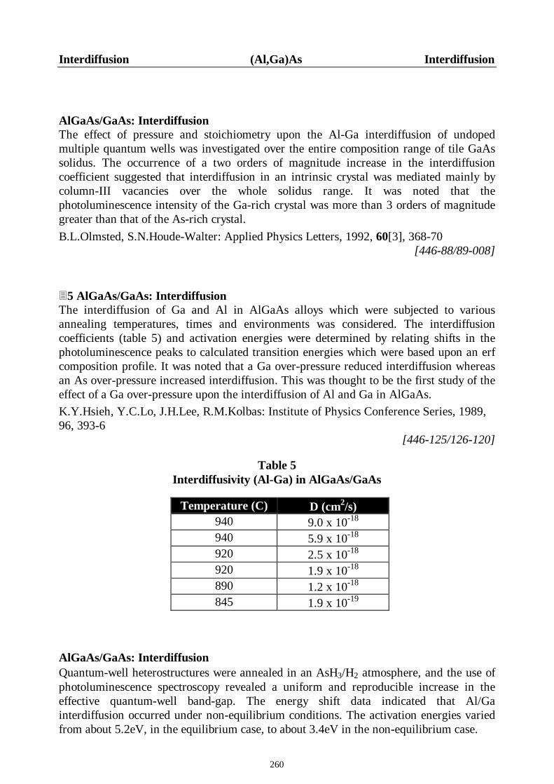
34 AlGaAs/GaAs: InterdiffusionData were presented which showed that the Al-Ga interdiffusion coefficient for anAlxGa1-xAs-GaAs quantum-well heterostructure or a superlattice was highly dependentupon the crystal encapsulation conditions (table 4). The activation energy for Al-Gainterdiffusion, and thus layer-disordering, was smaller (about 3.5eV) for dielectricencapsulated samples than after capless annealing (about 4.7eV). The interdiffusioncoefficient for Si3N4-capped samples was almost an order of magnitude smaller than forthe cases of capless or SiO2-capped samples at temperatures of between 800 and 875C.As well as the type of encapsulant, the encapsulation geometry (stripes or capped stripes)was important because of strain effects. These were a major source of anisotropic Al-Gainterdiffusion.L.J.Guido, N.Holonyak, K.C.Hsieh, R.W.Kaliski, W.E.Plano, R.D.Burnham,R.L.Thornton, J.E.Epler, T.L.Paoli: Journal of Applied Physics, 1987, 61[4], 1372-9
[446-60-002]

257
Interdiffusion (Al,Ga)As Interdiffusion
Table 4Interdiffusivity (Al-Ga) in AlGaAs/GaAs
Conditions Temperature (C) D (cm2/s)capless 875 1.1 x 10⁻¹⁷
SiO2 cap 875 9.6 x 10⁻¹⁸
capless 850 2.9 x 10⁻¹⁸
SiO2 cap 850 2.9 x 10⁻¹⁸
SiO2 cap 825 2.8 x 10⁻¹⁸
capless 825 1.0 x 10⁻¹⁸
Si3N4 cap 875 2.2 x 10⁻¹⁸
Si3N4 cap 850 7.8 x 10⁻¹⁹
SiO2 cap 800 7.0 x 10⁻¹⁹
capless 800 4.5 x 10⁻¹⁹
Si3N4 cap 825 3.8 x 10⁻¹⁹
Si3N4 cap 800 2.2 x 10⁻¹⁹
AlGaAs/GaAs: InterdiffusionA model was presented which described the diffusion of Si into GaAs from grown-indopant sources. The effects of background impurities upon Si diffusion and layerinterdiffusion in the present superlattices were also described. Epitaxial GaAs sampleswith alternating doped and undoped layers, and superlattices with Mg- or Si-doped layers,were studied. Various annealing conditions were used to study interactions betweengrown-in impurities and native defects. A model which described impurity diffusion andAl-Ga layer interdiffusion was based upon the behavior of column-III vacancies (VIII) andinterstitials (IIII), and the control of their contents. The results indicated that n-typesuperlattices underwent enhanced layer interdiffusion because of an increased solubilityof the VIII defect. Enhanced layer interdiffusion in p-type superlattices was attributed toan enhanced solubility of IIII.D.G.Deppe, N.Holonyak, W.E.Plano, V.M.Robbins, J.M.Dallesasse, K.C.Hsieh,J.E.Baker: Journal of Applied Physics, 1988, 64[4], 1838-44
[446-72/73-006]
AlGaAs/GaAs: InterdiffusionIt was shown that donor diffusion and layer intermixing were greatly enhanced in thepresence of defects which were created by crystal overgrowth on locally laser-meltedsubstrates. Accelerated defect and impurity-induced layer disordering, and donordiffusion from a solid SiO2 source, a Ge vapor source or a grown-in Se source were

258
Interdiffusion (Al,Ga)As Interdiffusion
observed in regions of high defect density. Enhanced donor diffusion and crystal self-diffusion were attributed to an increased density of column-III defects and dislocations.F.A.Kish, W.E.Plano, K.C.Hsieh, A.R.Sugg, N.Holonyak, J.E.Baker: Journal of AppliedPhysics, 1989, 66[12], 5821-5
[446-74-005]
AlGaAs/GaAs: InterdiffusionA study was made of the in-diffusion of various group-IV and group-VI n-type impurities.In all cases, the n-type dopants enhanced the Al-Ga interdiffusion coefficient above thatwhich could be attributed to an As over-pressure alone. The Si-induced enhancement hadpreviously been attributed to a change in Fermi-level position with doping and couldtherefore account for disordering by other n-type impurities. However, importantdifferences were observed in the interdiffusion characteristics that were induced by Si orGe, and by S or Se. The disordering was attributed to an enhancement of the group-IIIvacancy concentration for each of these n-type impurities. This was also true of undopedcrystals which were disordered by an As ambient alone at 855C.B.L.Olmsted, S.N.Houde-Walter: Applied Physics Letters, 1993, 62[13], 1516-8
[446-106/107-016]
AlGaAs/GaAs: InterdiffusionThe As vapor pressure dependence of interdiffusion in a hetero-interface at hightemperatures was studied by measuring the wavelength shift of the photoluminescence ina multi quantum well. It was found that interdiffusion at a temperature of 850C wasminimized by an As pressure of 100torr and was enhanced at both lower and higher Aspressures. A degradation of the photoluminescence intensity was observed only at higherAs pressures. These effects were attributed to the presence of excess Al and Gavacancies, and their associated defects.A.Furuya, O.Wada, A.Takamori, H.Hashimoto: Japanese Journal of Applied Physics,1987, 26[6], L926-8
[446-55/56-002]
AlGaAs/GaAs: InterdiffusionTransmission electron microscopy and carrier concentration measurements were used tocharacterize the layer interdiffusion mechanism of a Se-doped AlxGa1-xAs-GaAssuperlattice during high-temperature annealing. By varying the annealing environmentand comparing the results with similarly annealed un-doped superlattices and Mg-dopedsuperlattices, it was found that layer interdiffusion occurred via the interaction of the Seimpurity with native defects which were associated with As-rich conditions. The mostlikely candidate was suggested to be the column-III vacancy.D.G.Deppe, N.Holonyak, K.C.Hsieh, P.Gavrilovic, W.Stutius, J.Williams. AppliedPhysics Letters, 1987, 51[8], 581-3
[446-55/56-002]
259
Interdiffusion (Al,Ga)As Interdiffusion
AlGaAs/GaAs: InterdiffusionA study was made of the role of defect diffusion, from crystal surfaces, in the disorderingof a multiple quantum well structure that was Si-doped during molecular beam epitaxialgrowth. The distribution of the native defects was deduced from photoluminescencespectroscopic, secondary ion mass spectrometric, and electrochemical C-V profiling data.No significant difference was observed between the Al-Ga interdiffusion coefficients ofSi-doped and undoped superlattices when they were annealed with excess Ga. This wasattributed to the lack of a source of group-III vacancies. Only a small fraction of theenhancement which was predicted to result from Si doping was observed when excess Aswas used instead. The largest Fermi-level enhancement was observed when no excess Gaor As was present in the evacuated ampoule. The results indicated that the crystal surfacewas both source and sink for the native defects which were known to mediate Al-Gainterdiffusion. Significant electrical compensation of the donors was observed afterannealing in both As-rich or Ga-rich ambients. This was attributed to ionized group-IIIvacancy generation in the former case, and to Si atoms which moved from group-III togroup-V sites in the latter case.B.L.Olmsted, S.N.Houde-Walter: Applied Physics Letters, 1993, 63[8], 1131-3
[446-106/107-017]
AlGaAs/GaAs: InterdiffusionSpatially resolved values of the Al/Ga interdiffusion coefficient for p-i-n and n-i-pAlGaAs-GaAs device structures were found to be almost identical in magnitude, butvaried with position (by a factor of 2) across a 1µ-thick multiple quantum well activeregion. These observations contrasted with theoretical predictions, given that the Fermilevel to valence-band energy separation changed by 0.7eV across the intrinsic region, andsuggested that impurity-free layer disordering did not provide the necessary uniformity inenergy shift for photonic integrated circuit fabrication.S.Seshadri, L.J.Guido, P.Mitev: Applied Physics Letters, 1995, 67[4], 497-9
[446-123/124-157]
AlGaAs/GaAs: InterdiffusionDirect optical observations were made of diffusion-related deep levels that wereassociated with interdiffusion in superlattice structures. Low-energy cathodoluminescencespectroscopy was used to investigate the formation and evolution of deep levels undervarious conditions. It was found that the spatial distribution of the deep levels wasstrongly related to the extent of superlattice intermixing, as measured using secondary ionmass spectrometry and photoluminescence spectroscopy. The results strongly suggestedthat a larger interdiffusion rate of the Si-induced layer intermixing was related to theformation of a deep level which was associated with an optical emission at 1.3eV.R.E.Viturro, B.L.Olmsted, S.N.Houde-Walter, G.W.Wicks: Journal of Vacuum Scienceand Technology B, 1991, 9[4], 2244-50
[446-88/89-008]
260
Interdiffusion (Al,Ga)As Interdiffusion
AlGaAs/GaAs: InterdiffusionThe effect of pressure and stoichiometry upon the Al-Ga interdiffusion of undopedmultiple quantum wells was investigated over the entire composition range of tile GaAssolidus. The occurrence of a two orders of magnitude increase in the interdiffusioncoefficient suggested that interdiffusion in an intrinsic crystal was mediated mainly bycolumn-III vacancies over the whole solidus range. It was noted that thephotoluminescence intensity of the Ga-rich crystal was more than 3 orders of magnitudegreater than that of the As-rich crystal.B.L.Olmsted, S.N.Houde-Walter: Applied Physics Letters, 1992, 60[3], 368-70
[446-88/89-008]
35 AlGaAs/GaAs: InterdiffusionThe interdiffusion of Ga and Al in AlGaAs alloys which were subjected to variousannealing temperatures, times and environments was considered. The interdiffusioncoefficients (table 5) and activation energies were determined by relating shifts in thephotoluminescence peaks to calculated transition energies which were based upon an erfcomposition profile. It was noted that a Ga over-pressure reduced interdiffusion whereasan As over-pressure increased interdiffusion. This was thought to be the first study of theeffect of a Ga over-pressure upon the interdiffusion of Al and Ga in AlGaAs.K.Y.Hsieh, Y.C.Lo, J.H.Lee, R.M.Kolbas: Institute of Physics Conference Series, 1989,96, 393-6
[446-125/126-120]
Table 5Interdiffusivity (Al-Ga) in AlGaAs/GaAs
Temperature (C) D (cm2/s)940 9.0 x 10⁻¹⁸
940 5.9 x 10⁻¹⁸
920 2.5 x 10⁻¹⁸
920 1.9 x 10⁻¹⁸
890 1.2 x 10⁻¹⁸
845 1.9 x 10⁻¹⁹
AlGaAs/GaAs: InterdiffusionQuantum-well heterostructures were annealed in an AsH3/H2 atmosphere, and the use ofphotoluminescence spectroscopy revealed a uniform and reproducible increase in theeffective quantum-well band-gap. The energy shift data indicated that Al/Gainterdiffusion occurred under non-equilibrium conditions. The activation energies variedfrom about 5.2eV, in the equilibrium case, to about 3.4eV in the non-equilibrium case.

261
Interdiffusion (Al,Ga)As Interdiffusion
S.Seshadri, L.J.Guido, T.S.Moise, J.C.Beggy, T.J.Cunningham, R.C.Barker, R.N.Sacks:Journal of Electronic Materials, 1992, 21[1], 33-8
[446-93/94-004]
GaAlAs/GaAs: InterdiffusionA study was made of Al-Ga interdiffusion and C acceptor diffusion in C-dopedGa0.6Al0.4As/GaAs superlattices which had been annealed, under various ambient As4pressure conditions, at temperatures ranging from 825 to 960C. The superlattices weredoped with C to an initial acceptor concentration of about 2.9 x 10¹⁹/cm3. The Al-Gainterdiffusion was found to be most predominant in Ga-rich annealing ambients. Theinterdiffusivity values were about 2 orders of magnitude lower than those predicted by theFermi-level effect model. In As-rich ambients, the interdiffusion values were inapproximate agreement with those which were predicted by the Fermi-level effect model.By analyzing measured hole concentration profiles, it was deduced that both C acceptordiffusion and reduction occurred during annealing. Both the C acceptor diffusivity andthe C acceptor reduction coefficient data could be characterized approximately by a ¼-power dependence upon the As4 pressure. These pressure dependences indicated that Cdiffused via the interstitialcy or interstitial-substitutional mechanism, while hole reductionwas governed by a C acceptor precipitation mechanism.H.M.You, T.Y.Tan, U.M.Gösele, S.T.Lee, G.E.Höfler, K.C.Hsieh, N.Holonyak: Journalof Applied Physics, 1993, 74[4], 2450-60
[446-109/110-028]
GaAlAs/GaAs: InterdiffusionSuperlattices of Ga0.7Al0.3As/GaAs which had been grown by means of metalorganicchemical vapor deposition, and which were heavily doped with C using CCl4, wereannealed (825C, 24h) under various ambients and encapsulants. Photoluminescencemonitoring at 1.7K was used to determine approximate interdiffusion coefficients, DAl-Ga,for various annealing conditions. For all of the encapsulants which were studied, DAl-Ga
increased with increasing As4 pressure in the annealing ampoule. This result disagreedwith trends which had been reported for Mg-doped crystals, and with the predictions ofthe charged point-defect (Fermi-level) model. It was noted that a Si3N4 cap provided themost effective surface protection against ambient-stimulated layer interdiffusion (DAl-Ga =1.5 x 10⁻¹⁹ to 3.9 x 10⁻¹⁹cm2/s). The most extensive layer intermixing occurred foruncapped superlattices which were annealed in an As-rich ambient (DAl-Ga equal to about3.3 x 10-18cm2/s). These values were up to 40 times greater than those which hadpreviously been reported for nominally undoped AlGaAs/GaAs superlattices. Thisimplied that doping slightly enhanced layer intermixing; but this was significantly lessthan that predicted by the Fermi-level effect. The discrepancies between the experimentaldata and the model were considered. Marked changes in the optical properties of theannealed superlattices, as a function of storage time at room temperature, were alsoreported. It was suggested that these changes might reflect a degraded thermal stability ofthe annealed crystals, due to lattice defects which were generated at high temperatures. It

262
Interdiffusion (Al,Ga)As Interdiffusion
was proposed that this was related to the failure to prepare buried heterostructurequantum-well lasers, via impurity-induced layer disordering, in similar doped crystals.I.Szafranek, M.Szafranek, J.S.Major, B.T.Cunningham, L.J.Guido, N.Holonyak,G.E.Stillman: Journal of Electronic Materials, 1991, 20[6], 409-18
[446-91/92-005]
36 GaAlAs/GaAs: InterdiffusionThe migration of Al and Ga in Ga0.6Al0.4As/GaAs quantum wells was investigated bymeasuring the photoluminescence of samples which had been annealed at temperaturesranging from 850 to 1065C; with and without a SiO2 cap. At 1000C, under a SiO2 cap,the Al-Ga interdiffusion coefficient was at least 2 orders of magnitude higher for aGaAlAs/GaAs quantum well than for an InAlGaP/GaInP quantum well, within the samesample. By comparing the calculated photoluminescence shifts with measured values, anactivation energy of 4.5eV was estimated (table 6) for Al-Ga interdiffusion in aGaAlAs/GaAs quantum well under a SiO2 cap.K.J.Beernink, D.Sun, D.W.Treat, B.P.Bour: Applied Physics Letters, 1995, 66[26], 3597-9
[446-125/126-120]
Table 6Interdiffusivity (Al-Ga) in GaAlAs/GaAs
Conditions Temperature (C) D (cm2/s)RTA/SiO2 1065 2.5 x 10⁻¹⁵
RTA/SiO2 1025 1.8 x 10⁻¹⁵
RTA/SiO2 1000 4.3 x 10⁻¹⁶
no SiO2 1000 4.1 x 10⁻¹⁷
RTA/SiO2 975 1.8 x 10⁻¹⁶
FA/SiO2 925 3.0 x 10⁻¹⁷
FA/SiO2 900 2.3 x 10⁻¹⁷
FA/SiO2 870 4.7 x 10⁻¹⁸
FA/SiO2 845 1.6 x 10⁻¹⁸
263
(Al,Ga,In)P
Si
InAlGaP/GaAs: Si DiffusionThe diffusion of SiIII-SiV neutral pairs versus the diffusion of SiIII-VIII complexes in III-Vcrystals was considered with regard to experimental data which revealed the effect of Sidiffusion upon the self-diffusion of column-III and column-V lattice atoms. Secondaryion mass spectroscopy was used to compare the enhanced diffusion of column-III orcolumn-V atoms in various Si-diffused heterostructures which were closely lattice-matched to GaAs. An enhancement of lattice atom self-diffusion, due to impuritydiffusion, was found to occur predominantly on the column-III lattice. The data supportedthe SiIII-VIII diffusion model and indicated that the main native defects whichaccompanied Si diffusion were column-III vacancies. These diffused directly on thecolumn-III sub-lattice.D.G.Deppe, W.E.Plano, J.E.Baker, N.Holonyak, M.J.Ludowise, C.P.Kuo, R.M.Fletcher,T.D.Osentowski, M.G.Craford: Applied Physics Letters, 1988, 53[22], 2211-3
[446-64/65-157]
Zn
AlGaInP: Zn DiffusionThe behavior of Zn acceptors in p-type layers during thermal annealing in gaseous AsH3-H2 mixtures was investigated. It was found that the electrical activity of Zn acceptors wasgreatly affected by H atoms which originated from the arsine during annealing. Inaddition, observations of atomic disordering suggested that H passivation of Zn acceptorssuppressed atomic diffusion. The results could be consistently explained by a simple Hpassivation model which involved the termination of dangling bonds by H atoms.A.Ishibashi, M.Mannoh, I.Kidoguchi, Y.Ban, K.Ohnaka: Applied Physics Letters, 1994,65[10], 1275-7
[446-119/120-188]

264
Interdiffusion (Al,Ga,In)P|(Al,Ga)Sb Be
Interdiffusion
InAlGaP/GaInP: InterdiffusionThe migration of Al and Ga in In0.5Al0.3Ga0.2P/Ga0.6In0.4P quantum wells wasinvestigated by measuring the photoluminescence of samples which had been annealed attemperatures ranging from 850 to 1065C; with and without a SiO2 cap. At 1000C, under aSiO2 cap, the Al-Ga interdiffusion coefficient was at least 2 orders of magnitude higherfor a GaAlAs/GaAs quantum well, than for an InAlGaP/GaInP quantum well, within thesame sample.K.J.Beernink, D.Sun, D.W.Treat, B.P.Bour: Applied Physics Letters, 1995, 66[26], 3597-9
[446-125/126-120]
(Al,Ga)Sb
Be
AlGaSb: Be DiffusionThe ion-implantation p-type doping of Al0.75Ga0.25Sb was studied. The surfacemorphology and electrical properties were shown, by using atomic force microscopy andHall measurements, to be degraded after rapid thermal annealing at 650C. Theimplantation of Be resulted in sheet hole concentrations which were twice those of theimplanted acceptor dose (1013/cm2) after 600C annealing. This was attributed to doubleacceptor or antisite defect formation. Implanted C acted as an acceptor, but alsodemonstrated an excess hole conduction which was attributed to implantation-induceddefects. Implanted Zn required a higher annealing temperature than did Be, in order toachieve 100% effective activation for a dose of 1013/cm2. It was suggested that this wasprobably the result of the greater implantation-induced damage that was created by the
265
Be (Al,Ga)Sb Mg
heavier Zn ion. The secondary ion mass spectroscopy of as-implanted and annealed Be,Mg and C samples was studied. The diffusion of implanted Be (5 x 1013cm2, 45keV) wasshown to exhibit an inverse dependence upon temperature. This was attributed to asubstitutional-interstitial diffusion mechanism. Implanted C (2.5 x 10¹⁴/cm2, 70keV)exhibited no redistribution, even after annealing at 650C.J.C.Zolper, J.F.Klem, A.J.Howard, M.J.Hafich: Journal of Applied Physics, 1996, 79[3],1365-70
[446-131/132-168]
Mg
AlGaSb: Mg DiffusionThe ion-implantation p-type doping of Al0.75Ga0.25Sb was studied. The surfacemorphology and electrical properties were shown, by using atomic force microscopy andHall measurements, to be degraded after rapid thermal annealing at 650C. Theimplantation of Mg resulted in sheet hole concentrations which were twice those of theimplanted acceptor dose (1013/cm2) after 600C annealing. This was attributed to doubleacceptor or antisite defect formation. Implanted C acted as an acceptor, but alsodemonstrated an excess hole conduction which was attributed to implantation-induceddefects. Implanted Zn required a higher annealing temperature than did Mg, in order toachieve 100% effective activation for a dose of 1013/cm2. It was suggested that this wasprobably the result of the greater implantation-induced damage that was created by theheavier Zn ion. The secondary ion mass spectroscopy of as-implanted and annealed Mgand C samples was studied. Implanted Mg (1014/cm2, 110keV) exhibited markedredistribution, and losses of up to 56% at the interface, after 600C annealing. Implanted C(2.5 x 10¹⁴/cm2, 70keV) exhibited no redistribution, even after annealing at 650C.J.C.Zolper, J.F.Klem, A.J.Howard, M.J.Hafich: Journal of Applied Physics, 1996, 79[3],1365-70
[446-131/132-168]
266
(Al,In)As
Be
InAlAs: Be DiffusionThe behavior of implanted Be+ ions was investigated during rapid thermal annealing attemperatures of between 600 and 900C. It was found that the apparent activation energyfor Be was equal to 0.43eV. Lower activation efficiencies of the dopant were found inInAlAs, as compared with InGaAs. Anomalously low activation was detected for low-dose Be implants. The latter effect was attributed to a lack of vacant sites for the Beatoms to occupy. Extensive redistribution of the Be was observed after annealing (750C,10s).E.Hailemariam, S.J.Pearton, W.S.Hobson, H.S.Luftman, A.P.Perley: Journal of AppliedPhysics, 1992, 71[1], 215-20
[446-86/87-038]
Fe
InAlAs: Fe DiffusionSingle (200keV) and multiple-energy Fe implantation of n-type material was carried outon In0.52Al0.48As at room temperature or 200C. Secondary ion mass spectrometry profilesrevealed marked out-diffusion during all of the rapid thermal annealing treatments whichwere used; regardless of the implantation temperature. The Fe implantation peaks whichwere observed after the annealing of other In-based compounds were not observed here.J.M.Martin, R.K.Nadella, M.V.Rao, D.S.Simons, P.H.Chi, C.Caneau: Journal ofElectronic Materials, 1993, 22[9], 1153-8
[446-109/110-039]
Si
InAlAs: Si DiffusionThe behavior of implanted Si+ ions was investigated during rapid thermal annealing attemperatures of between 600 and 900C. The apparent activation energy for Si was equal

267
Si (Al,In)As General
to 0.58eV. Lower activation efficiencies of the dopant were found in InAlAs, ascompared with InGaAs. The Si underwent no migration, even after annealing at 850C.E.Hailemariam, S.J.Pearton, W.S.Hobson, H.S.Luftman, A.P.Perley: Journal of AppliedPhysics, 1992, 71[1], 215-20
[446-86/87-038]
Ti
InAlAs: Ti DiffusionThe Ti implantation of p-type material was carried out on In0.52Al0.48As at roomtemperature or 200C. The implanted Ti exhibited only slight in-diffusion and out-diffusion after both room temperature and 200C implantation. Rutherford back-scatteringmeasurements of annealed samples which had been implanted at 200C revealed a crystalquality which was similar to that of virgin material. The resistivity of all of the samplesafter annealing was greater than 106 Ω cm.J.M.Martin, R.K.Nadella, M.V.Rao, D.S.Simons, P.H.Chi, C.Caneau: Journal ofElectronic Materials, 1993, 22[9], 1153-8
[446-109/110-039]
General
InAlAs: DiffusionIt was shown that systematic variations in the experimental parameters could turn multi-layers into so-called microscopic laboratories for the study of point defects. In this way,the effects of composition, doping and strain could be separated. It was also possible todetermine the nature and charge state of the mediating defect. The present results showedthat interdiffusion in the present system was mediated by a double-acceptor vacancy-likedefect. The activation energy, in the case of In0.52Al0.48As, was equal to 4eV. Its valuevaried to the extent of 0.051eV for every percent of strain.F.H.Baumann, J.H.Huang, J.A.Rentschler, T.Y.Chang, A.Ourmazd: Physical ReviewLetters, 1994, 73[3], 448-51
[446-115/116-141]

268
AlN
Figure 2: Diffusivity of O in AlN
D
AlN: D DiffusionThe out-diffusion of H was studied, using 2H plasma-treated (250 or 400C, 0.5h) or 2H+-implanted samples, during annealing at temperatures ranging from 300 to 900C.
1.0E-16
1.0E-15
1.0E-14
1.0E-13
1.0E-12
1.0E-11
1.0E-10
1.0E-09
1.0E-08
1.0E-07
4 5 6
table 7table 8table 9
104/T(K)
D (c
m2 /s
)

269
D AlN O
Secondary ion mass spectrometry was used to measure the resultant distributions. Atconcentrations that were greater than 1020/cm3, there was a near-surface (less than 0.3µ)region that was probably due to the formation of platelet defects. At concentrations ofabout 1018/cm3, a plateau region was present which extended throughout the filmthickness of about 1µ. This was attributed to the pairing of 2H with point defects. Inimplanted samples, 2H redistribution occurred in the same manner as the bulk populationin plasma-treated material. The thermal stability of the D profile in the nitride was muchhigher than that in GaAs and similar compounds.R.G.Wilson, S.J.Pearton, C.R.Abernathy, J.M.Zavada: Journal of Vacuum Science andTechnology A, 1995, 13[3], 719-23
[446-140-029]
Table 7Diffusivity of O in AlN
Temperature (C) D (cm2/s)1500 8.0 x 10⁻¹⁶
1600 3.5 x 10⁻¹⁵
1700 6.7 x 10⁻¹⁵
1800 1.3 x 10⁻¹⁴
1900 1.9 x 10⁻¹⁴
N
AlN: N PermeationA method was described for the determination of ion migration numbers on the basis ofpermeability data. The latter data were here obtained by using an emf technique. Thepermeability was equal to 8.66cm2/MPa-s. It was pointed out that the present methodcould establish the presence of an ionic component of the conductivity for nitrides, and itsimportance could be estimated for cases where a dense ceramic could not be prepared.R.P.Lesunova, L.S.Karenina, V.K.Gilderman, S.F.Palguev: Izvestiya Akademii NaukSSSR - Neorganicheskie Materialy, 1989, 25[11], 1926-8. (Inorganic Materials, 1989,25[11], 1633-5)
[446-76/77-131]
O
37 AlN: O DiffusionInterdiffusion of N and O was investigated by means of electron energy-loss spectroscopyand transmission electron microscopy. Diffusion couples, Al2O3/AlN, were prepared byoxidizing AlN ceramics, and were annealed at temperatures ranging from 1500 to 1900C

270
O AlN O
(table 7). The couples were encapsulated in a Ta ampoule in order to ensure an inertatmosphere, and the O concentration profiles across the oxide/nitride interface weremeasured by means of electron energy-loss spectroscopy. It was found that O/Ninterdiffusion in AlN could be described by:
D(cm2/s) = 1.5 x 10⁻⁸ exp[-240(kJ/mol)/RT]The magnitude and temperature-dependence of the interdiffusion were comparable tothose which had been reported for other non-oxide ceramic materials. Under normal AlNsintering conditions, the O/N interdiffusion was too slow to provide an effective meansfor O removal from AlN grains.M.Sternitzke, G.Müller: Journal of the American Ceramic Society, 1994, 77[3], 737-42
[446-123/124-267]
Table 8Bulk Diffusivity of O in AlN
Temperature (C) D (cm2/s)1600 3.43 x 10⁻¹⁴
1700 1.00 x 10⁻¹³
1800 4.27 x 10⁻¹³
1900 1.43 x 10⁻¹²
38,9 AlN: O Grain Boundary DiffusionThe diffusion of O in commercial nitride substrates was studied by carrying outinterdiffusion-type experiments. The diffusion of O within AlN grains and along grainboundaries was investigated. By using as-received AlN substrates and an electronmicroprobe as an analytical tool, it was found that the rate of O diffusion along grainboundaries was strongly affected by the presence of impurities and/or other phases atthese boundaries. The diffusion of O within AlN grains was studied at temperatures ofbetween 1600 and 1900C (table 8) in a flowing N atmosphere by using secondary ionmass spectrometry to determine O concentration profiles. The chemical diffusioncoefficient of O in the AlN lattice was described by:
log[D(cm2/s)] = -1.68 - 427(kJ/mol)/2.303RTThe O concentration profiles which were determined by means of secondary ion massspectrometry also revealed a contribution that arose from diffusion along grain boundaries(table 9). It was therefore possible to determine values of the product of grain boundarywidth and grain boundary O diffusivity.H.Solmon, D.Robinson, R.Dieckmann: Journal of the American Ceramic Society, 1994,77[11], 2841-8
[446-123/124-268]

271
Interdiffusion AlN Interdiffusion
Interdiffusion
AlN/Al2OC: InterdiffusionIt was recalled that AlN and Al2OC were isostructural. The AlN-Al2OC system formedhomogeneous solid solutions above 1950C. Interdiffusion was studied in the solid-solution regime in order to clarify differences in the kinetics of phase separation whensamples were annealed at lower temperatures. The diffusion couples, (AlN)0.7(Al2OC)0.3
/(AlN)0.3(Al2OC)0.7, were prepared by hot pressing and were annealed at 2273K. It wasfound that the interdiffusion coefficients in this system were much larger than those in theSiC-AlN system.Q.Tian, A.V.Virkar: Journal of the American Ceramic Society, 1996, 79[8], 2168-74
[446-150/151-214]
Table 9Grain Boundary Diffusivity of O in AlN
Temperature (C) D (cm2/s)1700 9.50 x 10⁻¹⁰
1800 1.59 x 10⁻⁹
1900 1.78 x 10⁻⁸
AlN/SiC: InterdiffusionIt was recalled that AlN and 2H-type SiC were isostructural. The SiC-AlN system formedhomogeneous solid solutions above 2000C. Interdiffusion was studied in the solid-solution regime in order to clarify differences in the kinetics of phase separation duringannealing at lower temperatures. Diffusion couples, (SiC)0.3(AlN)0.7/(SiC)0.7(AlN)0.3,were prepared by hot pressing. Interdiffusion coefficients were measured at 2373, 2473and 2573K, and the corresponding activation energy was estimated to be 632kJ/mol.Q.Tian, A.V.Virkar: Journal of the American Ceramic Society, 1996, 79[8], 2168-74
[446-150/151-214]

272
BN
D
BN: D DiffusionRe-emission curves and thermodesorption spectra were measured for D ions which hadbeen implanted into this material. The thermodesorption spectra consisted of severalpeaks at temperatures ranging from 400 to 1100K. The re-emission curves could bedescribed by a simple mathematical model which included the effects of diffusion,second-order thermodesorption and defect trapping. The recycling factor and defect-trapping factor were found to depend exponentially upon the temperature, at temperaturesabove 600K. They deviated from this behavior at room temperature. It was supposed thatradiation-enhanced and thermally-activated processes predominated at room and hightemperatures, respectively.A.A.Pisarev, V.M.Smirnov, S.K.Zhdanov, A.V.Varava, V.V.Bandurko: Journal ofNuclear Materials, 1992, 187[3], 254-9
[446-91/92-075]
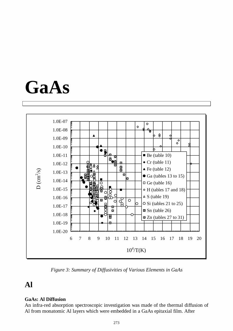
273
GaAs
Figure 3: Summary of Diffusivities of Various Elements in GaAs
Al
GaAs: Al DiffusionAn infra-red absorption spectroscopic investigation was made of the thermal diffusion ofAl from monatomic Al layers which were embedded in a GaAs epitaxial film. After
1.0E-20
1.0E-19
1.0E-18
1.0E-17
1.0E-16
1.0E-15
1.0E-14
1.0E-13
1.0E-12
1.0E-11
1.0E-10
1.0E-09
1.0E-08
1.0E-07
6 7 8 9 10 11 12 13 14 15 16 17 18 19 20
Be (table 10)Cr (table 11)Fe (table 12)Ga (tables 13 to 15)Ge (table 16)H (tables 17 and 18)S (table 19)Si (tables 21 to 25)Sn (table 26)Zn (tables 27 to 31)
104/T(K)
D (c
m2 /s
)
274
Al GaAs Al
annealing, the absorption peak of the 2-dimensionally localized vibrational modes at358/cm (due to Al layers) decreased while the peak at 362/cm (due to isolated Al atoms)increased. The 362/cm peak height was compared with the fraction of isolated Al atoms,as calculated by assuming second-nearest neighbor hopping diffusion from a monatomicAl layer and into the GaAs matrix. It was thus deduced that the diffusion coefficient of Alin GaAs was equal to 2 x 10-19cm2/s at 700C. It was concluded that this was a simple andreliable method for the investigation of impurity diffusion in crystals.H.Ono. N.Ikarashi, T.Baba: Applied Physics Letters, 1995, 66[5], 601-3
[446-121/122-053]
GaAs/Al/GaAs: Al DiffusionTheoretical and experimental aspects of the growth of heterostructures were investigated.In these heterostructures, GaAs was grown on top of the buried metal layer via migration-enhanced epitaxy at low temperatures (200 or 400C) in order to provide a kinetic barrierto the out-diffusion of Al during super-layer growth. The crystallinity and orientation ofthe Al film which was deposited on (100)GaAs at about 0C was studied by usingtransmission electron diffraction, dark-field imaging, and X-ray diffraction methods. Itwas found that the Al was polycrystalline, with a grain size of about 6nm, and that thepreferred growth orientation was (111). This could be textured in the plane, but orientedout of the plane. The quality of the GaAs super-layer, which was grown on top of the Alby means of migration-enhanced epitaxy, was very sensitive to the growth temperature. Alayer which was grown at 400C had a good structural and optical quality, but wasassociated with considerable Al out-diffusion at the Al/GaAs hetero-interface. At 200C,where the interface had good structural integrity, the super-layer exhibited twinning andno luminescence was observed.P.Bhattacharya, J.E.Oh, J.Singh, D.Biswas, R.Clarke, W.Dos Passos, R.Merlin,N.Mestres, K.H.Chang, R.Gibala: Journal of Applied Physics, 1990, 67[8], 3700-5
[446-78/79-030]
GaAs/AlAs: Al DiffusionThe implantation of Be ions into heterostructures at room temperature or liquid Ntemperatures was investigated. It was found that room-temperature implantation createddislocation loops at the first interface; a distance which was far short of the maximumprojected range. Implantation at low temperatures caused twinning. The latter could beremoved by annealing (900C, 1200s), without leading to the interdiffusion of Al. Thepresence of dislocation networks tended to enhance intermixing. The Be concentrationswere sufficiently low to prevent Be-induced intermixing.S.Mitra: Semiconductor Science and Technology, 1990, 5[11], 1138-40
[446-76/77-017]
GaAs/AlGaAs: Al DiffusionThe effect of room-temperature electron irradiation upon interdiffusion at quantum-wellinterfaces was investigated by using low-temperature cathodoluminescence spectroscopy.It was found that interdiffusion was enhanced by the presence of defects which were
275
Al GaAs As
generated by irradiation with a 400keV electron beam. After irradiation at roomtemperature to doses of between about 1.5 x 10¹⁷ and 2.5 x 10¹⁷/cm2, followed by rapidthermal annealing (900C, 60s), an interdiffusion length of 0.3 to 0.5nm was found. Theresultant damage tended to saturate with increasing irradiation dose. The formation ofdefect clusters at high doses limited the degree of defect introduction, and therefore theextent of interdiffusion at the interface.Y.J.Li, M.Tsuchiya, P.M.Petroff: Applied Physics Letters, 1990, 57[5], 472-4
[446-76/77-018]
GaAs/AlGaAs: Al DiffusionAn investigation was made of the proton-implantation enhanced intermixing of quantumwells, for H+ doses which ranged from 5 x 10¹³ to 1016/cm2. The implantation of 20keVH+, followed by high-temperature rapid thermal annealing, led to the enhanced diffusionof Al into the GaAs quantum well. Shifts in the electron heavy-hole recombinationenergies, due to compositional changes, were observed by using room-temperaturecathodoluminescence methods. Diffusion lengths of more than 2nm were deduced fromthe energy shifts in a 5nm well, and were found to depend upon the implanted dose andthe annealing time. It was suggested that this was to be expected if the enhancedinterdiffusion was caused by defects which were introduced by implantation.G.F.Redinbo, H.G.Craighead, J.M.Hong: Journal of Applied Physics, 1993, 74[5], 3099-102
[446-106/107-079]
As
GaAs: As DiffusionAtomistic thermodynamic calculations were made of the energetics of self-diffusion. Anassessment of the activation enthalpy of the saddle-point configuration of various modesof vacancy self-diffusion indicated that second-nearest neighbor hopping was the mostenergetically favorable mechanism, if vacancies were available in equilibriumconcentrations. An assessment of the activation entropy indicated that normal diffusionpre-exponential factors, of the order of 10-5 to 0.1cm2/s, were consistent with vacancyself-diffusion via second-nearest neighbor hopping. It was proposed that self-diffusionwhich was characterized by pre-exponential factors of the order of 107 to 108cm2/s, andactivation energies of the order of 6eV, involved processes in which surface vacancygeneration was inhibited and self-diffusion was mediated by Frenkel pair generation.J.F.Wager: Journal of Applied Physics, 1991, 69[5], 3022-31
[446-78/79-011]
GaAs: As DiffusionThe growth behavior and mechanisms of epitaxial lateral overgrowth of GaAs on (001)GaAs substrates were investigated. It was found that the lateral growth exhibited a strongdependence upon the orientation of the seed. Lateral growth was slowest when the aligned

276
As GaAs As
seed was oriented in the [100], [110], [010], [110], or equivalent, directions. However, itincreased sharply when the seed was tilted away from these orientations. Monomoleculargrowth steps on the surface, with a strong contrast and a high lateral spatial resolution,were successfully observed by using Nomarski differential interference contrastmicroscopy plus image processing. Their average propagation velocity was estimated tobe between 0.003 and 0.03mm/s. It was found that the surface of the epitaxial lateralovergrowth layer was extremely flat at the atomic scale. The experimental resultsindicated that vertical growth was governed mainly by the propagation of steps thatoriginated from their source. On the other hand, lateral growth was limited by thediffusion of As in Ga solution until (111)- or (001)-type facets appeared at the lateralgrowth front. The growth then became limited by kinetic processes. It was concluded thatsubstrates of (001)GaAs, as well as (111)GaAs, were suitable for obtaining a very smoothepitaxial lateral overgrowth layer with a large ratio of the lateral growth width to thevertical growth thickness.S.Zhang, T.Nishinaga: Journal of Crystal Growth, 1990, 99, 292-6
[446-76/77-007]
GaAs: As DiffusionThe chemical reactions and Schottky-barrier characteristics of W(200nm)/Si(0 to2.5nm)/GaAs contacts when annealed at 800C were investigated. The Si interfacial layersand W films were sputter-deposited onto chemically etched GaAs substrates. TheW/Si/GaAs diodes clearly exhibited the same Schottky-barrier characteristics as those of(WSi0.6)/GaAs diodes. By using secondary ion mass spectrometry, the Si layer was foundto suppress As atom diffusion from GaAs substrates and into W films during annealing(800C, 1h). A reduction in natively oxidized GaAs surfaces was also observed in theinitial stages of Si layer deposition by X-ray photo-emission spectroscopy. These resultssuggested that the Si layer eliminated native oxides from GaAs surfaces, resulting intungsten-silicide/GaAs intimate contact formation at the interface. The Si obstructed thediffusion paths of As atoms at W grain boundaries with W-Si-O ternary compounds.Y.Kuriyama, S.Ohfuji, J.Nagano: Journal of Applied Physics, 1987, 62[4], 1318-23
[446-55/56-005]
GaAs: As DiffusionThe in-diffusion of As vacancies, and their interaction with the mid-gap electron trap,EL2, during unprotected and proximity high-temperature annealing was modelled. Byfitting existing data, it was found that the diffusive capture of VAs by EL2 was inhibitedby a large (greater than 1eV) repulsive barrier of unknown origin. When taken togetherwith other published results, the model indicated that the diffusivity of VAs was describedby:
D(cm2/s) = 0.004 exp[-1.8(eV)/kT]However, this value was thought to be uncertain by at least an order of magnitude. A newdiscovery was the existence of a strong repulsive barrier between VAs and EL2. Thisinhibited their interaction, and was of the order of 1.2eV. When interpreted as being aCoulomb barrier, it required that EL2 (or a portion of EL2) should carry a positivecharge.

277
As GaAs As
In order to keep EL2 neutral, there would then have to be a compensating acceptor inEL2.K.M.Luken, R.A.Morrow: Journal of Applied Physics, 1996, 79[3], 1388-90
[446-134/135-124]
GaAs: As DiffusionQuantitative determinations were made of the contribution which As self-interstitialsmade to the As self-diffusion coefficient. Values of the As self-interstitial contributionwere deduced from S in-diffusion profiles, which were simulated on the basis of a kick-out mechanism.M.Uematsu, P.Werner, M.Schultz, T.Y.Tan, U.M.Gösele: Applied Physics Letters, 1995,67[19], 2863-5
[446-125/126-120]
GaAs: As DiffusionSamples with a 100nm Co over-layer, which had been subjected to rapid thermalannealing (400 to 650C, 60s), were analyzed by using mass and energy dispersive recoilspectrometry. Separate characterizations of the C, O, Co, Ga, and As depth distributionswere carried out. It was found that As migrated to the surface at annealing temperatureswhich were higher than 450C. The composition at various depths was determined at anumber of temperatures. On the basis of Arrhenius plots, the apparent activation energieswere estimated to be equal to about 0.6eV for phase formation and equal to 1.3eV fordiffusion. The X-ray diffraction data indicated that CoGa and CoAs were present in all ofthe annealed samples. Scanning electron microscopy showed that the surface wasreticulated after heat treatment, and that grain growth occurred at higher temperatures.M.Hult, H.J.Whitlow, M.Ostling, M.Andersson, Y.Andersson, I.Lindeberg, K.Stähl:Journal of Applied Physics, 1994, 75[2], 835-43
[446-117/118-165]
GaAs: As DiffusionAn investigation was made of near-bandedge photoluminescence from semi-insulatingcrystals after they had been annealed in wafer or bulk form. The results, with respect touniformity after annealing, were in agreement with previous data. The 1.360eV emissionband which was seen in annealed crystals and which had been assumed to imply that aVAs-related rapid-diffusion process was the mechanism which was responsible for theannealing-induced uniformity, was shown to be unconnected with it. The involvement ofVAs in the band was questioned. From literature data, it was estimated that the diffusioncoefficient of VAs (1.2 x 10⁻¹² at 1050C, 5.8 x 10⁻¹⁴ at 850C and 6.7 x 10⁻¹⁶cm2/s at 650C)was too low to permit bulk equilibrium and uniformity via vacancy diffusion from thesurface at the annealing temperatures which were used. It was concluded that localrearrangement of defects was a viable mechanism for producing uniformity during post-growth annealing.V.Swaminathan, R.Caruso, S.J.Pearton: Journal of Applied Physics, 1988, 63[6], 2164-7
[446-157/58-273]
278
As GaAs B
GaAs[l]: As DiffusionThe As concentration profiles ahead of a crystal interface, when advancing into a Ga-richsolution, were determined (during the electro-epitaxial growth of layers) by usingcomputer simulation techniques. The effects of Peltier heating or cooling, and ofelectromigration, during growth were incorporated. The growth velocity in the absence orpresence of convection, due to the Peltier effect and to electromigration, was calculatedunder various conditions. It was observed that there was a transition, in the movement ofAs atoms towards the crystal interface, from smooth and orderly to turbulent and wavy asthe intensity of the electric field increased during electro-epitaxial growth.R.S.Q.Fareed, R.Dhanasekaran, P.Ramasamy: Journal of Applied Physics, 1994, 75[8],3953-8
[446-117/118-165]
Au
GaAs: Au DiffusionRutherford back-scattering spectrometry and X-ray photoelectron spectroscopy were usedto investigate compositional changes, in thin metal-semiconductor systems, which werecaused by Ar+ and N+ ion bombardment or by annealing. The investigation was carriedout on contacts of Ni-Au-Ge on GaAs, as well as on irradiated and non-irradiated Au-GaAs. The structures were bombarded with Ar+ and N+ ions to doses of between 1014 and3 x 1016/cm2. The experimental results indicated that the interdiffusion of Au and Gaatoms depended upon the bombardment dose. Upon annealing the samples, blocking ofinterdiffusion was observed in Au-GaAs structures (which had been deposited on 50keVAr+ ion-irradiated and pre-treated GaAs) at certain radiation-defect concentrations. Thisbehavior was attributed to Au-Ga bond formation, and appeared to depend upon Gainterstitial atoms.L.B.Guoba, A.A.Vitkauskas, J.V.Kameneckas, V.R.Sargünas, A.P.Sakalas: PhysicaStatus Solidi A, 1989, 111[2], 507-13
[446-64/65-162]
B
GaAs: B DiffusionThe introduction of B into As sites, as deduced from the strength of vibrational modes at601.7 and 628.3/cm, was studied as a function of the fluence of 2MeV electrons.Simultaneous monitoring of the strength of the Is-2p electronic transitions of neutralshallow acceptors, and of the neutral 0.078eV acceptor and its singly-ionized 0.203eVlevel, provided accurate data on the position of the Fermi level during irradiation. Theresults were inconsistent with previous models for the location of B on As sites. A model
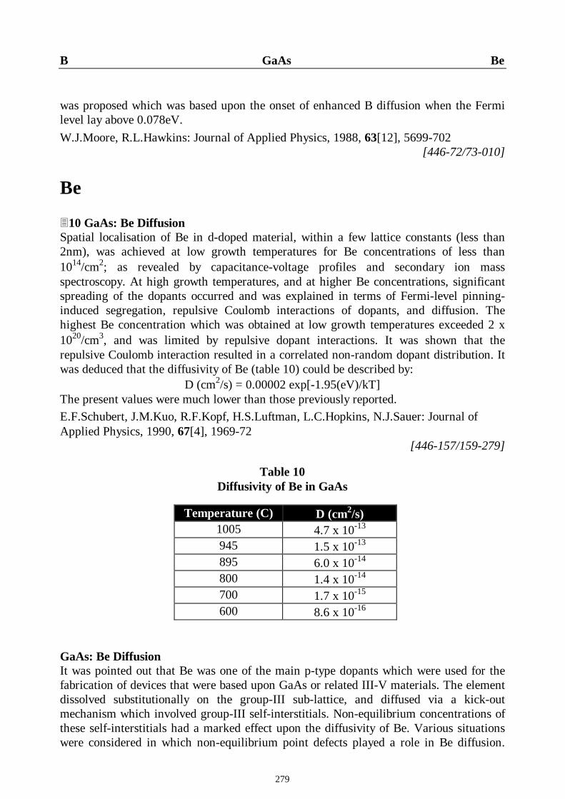
279
B GaAs Be
was proposed which was based upon the onset of enhanced B diffusion when the Fermilevel lay above 0.078eV.W.J.Moore, R.L.Hawkins: Journal of Applied Physics, 1988, 63[12], 5699-702
[446-72/73-010]
Be
310 GaAs: Be DiffusionSpatial localisation of Be in d-doped material, within a few lattice constants (less than2nm), was achieved at low growth temperatures for Be concentrations of less than1014/cm2; as revealed by capacitance-voltage profiles and secondary ion massspectroscopy. At high growth temperatures, and at higher Be concentrations, significantspreading of the dopants occurred and was explained in terms of Fermi-level pinning-induced segregation, repulsive Coulomb interactions of dopants, and diffusion. Thehighest Be concentration which was obtained at low growth temperatures exceeded 2 x10²⁰/cm3, and was limited by repulsive dopant interactions. It was shown that therepulsive Coulomb interaction resulted in a correlated non-random dopant distribution. Itwas deduced that the diffusivity of Be (table 10) could be described by:
D (cm2/s) = 0.00002 exp[-1.95(eV)/kT]The present values were much lower than those previously reported.E.F.Schubert, J.M.Kuo, R.F.Kopf, H.S.Luftman, L.C.Hopkins, N.J.Sauer: Journal ofApplied Physics, 1990, 67[4], 1969-72
[446-157/159-279]
Table 10Diffusivity of Be in GaAs
Temperature (C) D (cm2/s)1005 4.7 x 10⁻¹³
945 1.5 x 10⁻¹³
895 6.0 x 10⁻¹⁴
800 1.4 x 10⁻¹⁴
700 1.7 x 10⁻¹⁵
600 8.6 x 10⁻¹⁶
GaAs: Be DiffusionIt was pointed out that Be was one of the main p-type dopants which were used for thefabrication of devices that were based upon GaAs or related III-V materials. The elementdissolved substitutionally on the group-III sub-lattice, and diffused via a kick-outmechanism which involved group-III self-interstitials. Non-equilibrium concentrations ofthese self-interstitials had a marked effect upon the diffusivity of Be. Various situationswere considered in which non-equilibrium point defects played a role in Be diffusion.

280
Be GaAs Be
These included the in-diffusion of such dopants from an external source, the diffusion ofgrown-in dopants, self-interstitial generation by Fermi-level surface pinning, andrecombination-enhanced Be diffusion during device operation. It was noted that thediffusion behavior of C, which was found on the group-V sub-lattice of GaAs, was muchless sensitive to non-equilibrium point defects. It was therefore used to replace Be as a p-type dopant.M.Uematsu, K.Wada, U.Gösele: Applied Physics A, 1992, 55[4], 301-12
[446-93/94-008]
GaAs: Be DiffusionA study was made of the contributions of segregation, diffusion and aggregation to thebroadening of d-doped planes of Be. It was found that sharp spikes of Be could beobtained for sheet densities which were below 1013/cm2 and for growth temperatures of500C or less. At higher temperatures or densities, segregation or concentration-dependentrapid diffusion could occur; thus causing significant spreading even during growth. Theco-deposition of Si and Be markedly reduced this broadening.J.J.Harris, J.B.Clegg, R.B.Beall, J.Castagné, K.Woodbridge, C.Roberts: Journal ofCrystal Growth, 1991, 111[1-4], 239-45
[446-91/92-001]
GaAs: Be DiffusionThe slow positron technique was used to study undoped and Be-doped samples, andthereby determine the effect of Be upon the creation and migration of Ga vacancies, VGa,during annealing. It was deduced that a VGa mono-vacancy which was created in Be-doped material resulted in an enhanced Coulombic interaction between an As vacancy,VAs, and a Be acceptor, BeGa. In the case of undoped material, the formation of di-vacancies, VGa-VAs, predominated. The migration length of the vacancies was shorter inBe-doped material than in undoped material. It was therefore suggested that Gainterstitials, IGa, existed in the Be-diffused layer and interacted with VGa which wereintroduced from the surface. It was suggested that a kick-out mechanism governed Bediffusion in this material.J.L.Lee, L.Wei, S.Tanigawa, M.Kawabe: Journal of Applied Physics, 1991, 69[9], 6364-3
[446-86/87-009]
GaAs: Be DiffusionRecombination-enhanced impurity diffusion was observed for the first time in Be-dopedGaAs. It was found that Be diffusion under forward bias was enhanced by a factor ofabout 1015 at room temperature, and that the activation energy for diffusion decreasedfrom 1.8eV for thermal diffusion:
D(cm2/s) = 8.3 x 10⁻⁷ exp[-1.8(eV)/kT]to 0.6eV under recombination-enhanced conditions:
D(cm2/s) = 8.7 x 10⁻¹¹ exp[-0.59(eV)/kT]
281
Be GaAs Be
M.Uematsu, K.Wada: Applied Physics Letters, 1991, 58[18], 2015-7[446-84/85-013]
GaAs: Be DiffusionA close relationship between Be surface segregation and diffusion, in molecular beamepitaxial GaAs layers which were heavily doped with Be, was analyzed within theframework of a thermodynamic approach to segregation effects. Good agreement betweenthe theoretical and experimental results suggested that the main cause of extremely fastBe in-diffusion in Be-doped GaAs, and the deterioration of its surface morphology andluminescence properties, was Be surface segregation. This resulted in near-surface solid-phase layer enrichment with Be, as compared with bulk Be-doped GaAs. The effect ofgrowth parameters (excess As pressure, substrate temperature, growth rate) and dopantlevel upon the likelihood of Be segregation layer formation was considered.S.V.Ivanov, P.S.Kopev, N.N.Ledentsov: Journal of Crystal Growth, 1991, 108[3-4], 661-9
[446-81/82-002]
GaAs: Be DiffusionThe effect of the substrate orientation upon Be transport during GaAs molecular beamepitaxy was studied by means of secondary ion mass spectrometry. The substrates weremisoriented from (100) towards (111)A, and epitaxial growth was performed at 630C forBe dopant contents of between 5 x 10¹⁹ and 7 x 10¹⁹/cm3. Surface segregation andanomalous diffusion similarly depended upon the substrate orientation. In the case of the(311)A orientation, Be transport was sharply reduced from its value for the conventional(100) orientation. The results were explained qualitatively by considering the effect ofatomic steps upon the growing surface.K.Mochizuki, S.Goto, C.Kusano: Applied Physics Letters, 1991, 58[25], 2939-41
[446-81/82-009]
GaAs: Be DiffusionThe out-diffusion of implanted Be was found to be identical after capless or capped(nitride or oxide) rapid thermal annealing at temperatures of 900 to 1000C. It dependedupon the Be dose and its proximity to the surface. Out-diffusion was more pronouncedwhen the Be implant was shallow (less than 100nm) and/or the Be+ dose was high(greater than 1015/cm2). It was demonstrated that Be out-diffusion was driven by thepresence of a highly damaged surface layer. Auger results indicated the formation of aBeOx compound at the surface of a high-dose (1016/cm2) Be-implanted sample that wassubjected to capless rapid thermal annealing (1000C, 1s). It appeared that BeOx formationoccurred when the out-diffused Be interacted with native Ga/As oxides during annealing.All of the Be which remained in the GaAs, after rapid thermal annealing at temperaturesabove 900C for 2s, was electrically active.H.Baratte, D.K.Sadana, J.P.De Souza, P.E.Hallali, R.G.Schad, M.Norcott, F.Cardone:Journal of Applied Physics, 1990, 67[10], 6589-91
[446-78/79-012]

282
Be GaAs Be
GaAs: Be DiffusionHigh depth-resolution secondary ion mass spectrometry profiling was used to investigatethe broadening of d-doped planes of Be in material which had been prepared by usingmolecular beam epitaxial methods. It was confirmed that concentration-dependentdiffusion was the predominant broadening process for Be at growth temperatures of lessthan 600C. By incorporating Si atoms into the same plane, it was shown that thebroadening could be completely inhibited. This suggested that the rapid diffusion processresulted from mutual repulsion between the BeGa
- ions, and was prevented by the reversefield which arose from SiGa
+ ions or by the formation of low-mobility SiGa+-BeGa
-
complexes. The rapid diffusion of Si as SiGa-SiAs pairs was also reduced. The latter wasattributed to a Fermi-level effect, with compensation by Be tending to reduce theprobability of SiAs formation. The surface segregation of Si was unaffected, whereas thatof Be was reduced. This indicated that the surface fields which existed during growthcontributed to the behavior of Be, but not to that of Si.J.J.Harris, J.B.Clegg, R.B.Beall, J.Castagné: Semiconductor Science and Technology,1990, 5[7], 785-8
[446-76/77-007]
GaAs: Be DiffusionThe redistribution of Be implants during post-implantation annealing was studied in orderto evaluate the effect of implantation damage upon the diffusion process. The Be implantsexhibited only uniform concentration-dependent diffusion, unlike the rapid up-hilldiffusion which was observed in the peak of Mg implants. This difference was explainedby invoking a substitutional-interstitial diffusion mechanism and by performing computersimulations of damage-generated point defects. In the up-hill diffusion region, the dopantsdiffused from areas of excess interstitial concentration towards areas of excess vacancyconcentration. A critical point defect concentration was necessary in order to initiate up-hill diffusion. This behavior could be induced, in the case of Be implants, by co-implanting with a heavier element such as Ar.H.G.Robinson, M.D.Deal, D.A.Stevenson: Applied Physics Letters, 1990, 56[6], 554-6
[446-74-009]
GaAs: Be DiffusionThe behavior of implanted Be was studied by annealing samples which had beenimplanted with low or high Be doses. The high-dose (1014/cm2) samples exhibited anincrease in diffusion upon increasing the annealing temperature from 700 to 900C.However, the low-dose (2 x 10¹³/cm2) samples exhibited a decrease in diffusivity as thetemperature increased. The temperature dependence in the low-dose case could bereversed by the co-implantation of B (1014/cm2). This behavior was explained in terms of

283
Be GaAs Be
the substitutional-interstitial diffusion mechanism and the relative concentrations ofinterstitial and substitutional Be atoms in the various cases.M.D.Deal, H.G.Robinson: Applied Physics Letters, 1989, 55[10], 996-9
[446-72/73-010]
GaAs: Be DiffusionLayers of Be-doped material were grown at 300C by using the migration enhancedepitaxy technique. The layers exhibited essentially no electrical activation. Rapid thermalannealing of the layers resulted in a mobility and hole concentration which werecomparable to those of conventional molecular beam epitaxial layers which were grownat 600C. Secondary ion mass spectroscopy showed that Be diffusion in annealedmigration enhanced epitaxial layers was much smaller than that in conventional molecularbeam epitaxial layers; especially highly-doped ones. Raman spectroscopy and 4Kphotoluminescence experiments were also performed. It was concluded that the migrationenhanced epitaxy method could replace the conventional molecular beam epitaxy methodin applications which required a high hole concentration and little diffusion.B.Tadayon, S.Tadayon, W.J.Schaff, M.G.Spencer, G.L.Harris, P.J.Tasker, C.E.C.Wood,L.F.Eastman: Applied Physics Letters, 1989, 55[1], 59-61
[446-70/71-106]
GaAs: Be DiffusionAbrupt Be doping profiles were obtained by means of organometallic vapor phaseepitaxy. Secondary ion mass spectroscopy was used to study the annealing behavior ofprofiles for Be concentrations of 2 x 10¹⁸/cm3. The diffusion fronts were non-Gaussianand abrupt. Estimates of the diffusion coefficient of Be were obtained by assuming aquadratic concentration dependence. The Be diffusion coefficient was equal to about 10-
15 cm2/s at 825C. This was at least an order of magnitude lower than that reported for Znprofiles which were grown by means of organometallic vapor phase epitaxy. In addition,anomalous surface tailing growth was observed. This was very similar to that which wasreported to occur during Be doping via molecular beam epitaxy.M.J.Tejwani, H.Kanber, B.M.Paine, J.M.Whelan: Applied Physics Letters, 1988, 53[24],2411-3
[446-64/65-162]
GaAs: Be DiffusionA review was presented of self-diffusion mechanisms and doping-enhanced superlatticedisordering. With regard to the influence of Be p-type dopants, the Fermi level effect hadto be considered; together with dopant diffusion-induced Ga self-interstitialsupersaturation or undersaturation. In accord with its effect upon superlattice disordering,Be diffusion appeared to be governed by the kick-out mechanism. It was concluded thatdislocations in this material and in other III-V compounds were only moderately efficientsinks or sources for point defects.T.Y.Tan, U.Gösele: Materials Science and Engineering, 1988, B1, 47-65
[446-62/63-208]

284
Be GaAs Be
GaAs: Be DiffusionThe diffusion profiles of buried Be dopant which had been implanted by using a focussedion beam were determined after annealing. The diffusion coefficient of the Be wasdetermined by fitting the results of computer calculations. It was found that the diffusioncoefficient of the Be was enhanced by excess interstitial Be. The Be diffusion profilesexpanded upon annealing at 850C. The diffusion coefficient of Si which had beenintroduced by using a focussed ion beam was undetectably small when compared withthat of Be at 850C.T.Morita, J.Kobayashi, T.Takamori, A.Takamori, E.Miyauchi, H.Hashimoto: JapaneseJournal of Applied Physics, 1987, 26[8], 1324-7
[446-55/56-005]
GaAs: Be DiffusionModels were presented for the distribution profiles of Be in ion-doped layers afterimplantation and annealing. The possibility of predicting the mean free path of Be in III-V compounds was considered. The effect of defect-impurity interactions upon Bediffusion was also examined. It was found that a flux of impurities towards the surfaceoccurred which was not diffusive in nature.G.I.Koltsov, V.V.Makarov, S.J.Yurchuk: Fizika i Tekhnika Poluprovodnikov, 1996,30[10], 1907-16 (Semiconductors, 1996, 30[10], 996-1000)
[446-148/149-171]
GaAs: Be DiffusionAtomic-resolution images of Be delta-doped layers were obtained by means of cross-sectional scanning tunnelling microscopy. In the case of samples which had been grownat 480C, it was observed that the doping layer width for concentrations of up to 1013/cm2
was less than 1nm. At higher dopant concentrations, it was found that the dopant layerthickness increased markedly with dopant concentration. It was suggested that thisbroadening of the dopant layer at high dopant concentrations was due to Coulombicrepulsion between individual Be ions. The effect of Coulombic repulsion could also beobserved in the spatial distribution of the dopant atoms in the plane of the dopant layer.P.M.Koenraad, M.B.Johnson, H.W.M.Salemink, W.C.Van der Vleuten, J.H.Wolter:Materials Science and Engineering B, 1995, 35[1-3], 485-8
[446-136/137-109]
GaAs: Be DiffusionA study was made of the role that was played by the wafer surface in the transientdiffusion of Be. Samples were doped during molecular beam epitaxial growth, and wereannealed (900C, 0.25 or 2h) under 2 different caps. In some of the annealed samples, thedopant was initially located near to the surface. In other samples, the dopant was initiallylocated in a buried layer. Both types of sample were analyzed by means of secondary ionmass spectrometry. It was found that variations in the diffusion behavior under thevarious experimental conditions could all be qualitatively explained in terms of a model

285
Be GaAs Be
which took account of 3 important effects. These were the transient evolution of pointdefect populations, the injection of Ga vacancies by an oxide cap, and the efficiency ofthe surface in restoring point-defect equilibrium.Y.M.Haddara, M.D.Deal, J.C.Bravman: Applied Physics Letters, 1996, 68[14], 1939-41
[446-134/135-124]
GaAs: Be DiffusionThe migration of ion-implanted Be was studied as a function of Al concentration. Thebehavior of Be in AlGaAs was similar to that in GaAs, and it even exhibited theanomalous characteristic of increased redistribution with decreasing temperature. Theresults could be described by:
Ga0.8Al0.2As: D(cm2/s) = 1.8 x 10⁻⁹ exp[-0.90(eV)/kT]Ga0.6Al0.4As: D(cm2/s) = 3.3 x 10⁻⁹ exp[-0.84(eV)/kT]
GaAs: D(cm2/s) = 8.9 x 10⁻¹⁰ exp[-1.00(eV)/kT]The diffusivity of Be appeared to increase with Al content. This was suggested to be dueto an increase in the bond strength of matrix atoms upon adding Al. This prevented theeasy transfer of Be from interstitial to substitutional sites. An over-saturation of Beinterstitials could also explain the persistence of anomalous diffusion in AlGaAs withrespect to the annealing temperature. The results were explained in terms of asubstitutional-interstitial diffusion mechanism, the relative amounts of interstitial andsubstitutional Be, and the relative difficulty of moving from an interstitial to asubstitutional site.C.C.Lee, M.D.Deal, J.C.Bravman: Applied Physics Letters, 1995, 66[3], 355-7
[446-123/124-160]
GaAs: Be DiffusionThe diffusion of implanted Be in liquid-encapsulated Czochralski material was modelledby using a computer simulation. The so-called plus-one approach to defect generationafter implantation, as well as the assumed existence of local Ga interstitial sinks, weresuccessfully used to simulate a high Be diffusivity, up-hill diffusion and a time-dependentBi diffusivity. The fast diffusion of implanted Be could be simulated by using the sameintrinsic Bi diffusivity as that used in simulating the slow diffusion of molecular beamepitaxially grown-in Be. Account was taken of the roles which were played by extendeddefects and non-equilibrium Ga point defects in affecting the anomalous diffusionbehavior of implanted Be.J.C.Hu, M.D.Deal, J.D.Plummer: Journal of Applied Physics, 1995, 78[3], 1606-13
[446-123/124-161]
GaAs: Be DiffusionDiffusion was studied in samples of molecular beam epitaxial material with grown-in Be.The diffusion profiles of samples which had been annealed under various conditions weredetermined by using secondary ion mass spectrometry, and a computer simulation wasused to analyze the experimental results and extract diffusion parameters. The Be

286
Be GaAs Be
diffusion profiles exhibited kinks, and a time-dependent diffusivity, which weresuccessfully simulated. It was deduced that the intrinsic Be diffusivity was described by:
D(cm2/s) = 0.17 exp[-3.39(eV)/kT]J.C.Hu, M.D.Deal, J.D.Plummer: Journal of Applied Physics, 1995, 78[3], 1595-605
[446-123/124-161]
GaAs: Be DiffusionHeavily-doped polycrystalline material which had been grown by molecular beam epitaxyand metalorganic chemical vapor deposition was studied by using secondary ion massspectrometry and Hall measurements. It was found that Be rapidly diffused into theundoped buffer layer at a growth temperature of 450C. The concentration-depth profilesof Be in AlGaAs/GaAs heterojunction bipolar transistor layers indicated that Be diffusedmainly along grain boundaries.K.Mochizuki, T.Nakamura: Applied Physics Letters, 1994, 65[16], 2066-8
[446-119/120-191]
GaAs: Be DiffusionImplantation (1.5 x 10¹⁴/cm2) of 30keV Be into (x11)A-oriented semi-insulating GaAssubstrates (where x took values of up to 4) was carried out. For comparison, (110)- and(100)-oriented substrates were also implanted. It was found that the in-diffusion of Be in(311)A-oriented substrates was lower than that in (100) material.M.V.Rao, H.B.Dietrich, P.B.Klein, A.Fathimulla, D.S.Simons, P.H.Chi: Journal ofApplied Physics, 1994, 75[12], 7774-8
[446-117/118-166]
GaAs: Be DiffusionA study was made of the diffusion of Be in δ-doped layers of (111)A- or (100)-type, andof the evaporation of As atoms from the surfaces. It was found that the diffusion ofdopants in (111)A layers was slower than in (100), regardless of the presence of Asvacancies. On the other hand, diffusion in (100) layers was enhanced by the presence ofAs vacancies. It was noted that As atoms on the (111)A surface did not evaporate easily,as compared with those on the (100) surface.A.Shinoda, T.Yamamoto, M.Inai, T.Takebe, T.Watanabe: Japanese Journal of AppliedPhysics, 1993, 32[2-10A], L1374-6
[446-115/116-116]
GaAs: Be DiffusionAbnormal out-diffusion from heavily Be-doped material, prepared by molecular beamepitaxy, was found to be initiated by a decrease in the lattice constant of the p+ epilayer.From double-crystal X-ray spectra, Van der Pauw measurements, photoluminescence data,and infra-red absorption spectra for Be-doped material with various dopant concentrations,it was deduced that there existed a critical doping concentration (2.6 x 10¹⁹/cm3) beyondwhich the lattice constant of the epilayer began to decrease, and Be out-

287
Be GaAs Be
diffusion into the substrate was significantly enhanced. It was suggested that the tensilestress on the epilayer resulted in abnormal Be out-diffusion. The absorption coefficient,in the 8 to 10µ region, of Be-doped material with a carrier concentration of 8.3 x10¹⁹/cm3 was found to be about 104/cm.B.D.Liu, T.H.Shieh, M.Y.Wu, T.C.Chang, S.C.Lee, H.H.Lin: Journal of Applied Physics,1992, 72[7], 2767-72
[446-106/107-033]
GaAs: Be DiffusionSamples of n-type and p-type d-doped material, grown by molecular beam epitaxy andwith quite high doses of Be, were investigated by means of transmission electronmicroscopy. The magnitude of the doses ranged from half a monolayer to 2 monolayers.The microscopic structures of the d-doped regions and of the adjacent epilayers wereobserved directly. The effect of impurity spreading upon the hetero-interfaces andsuperlattices was studied. The Be atoms which were present in Be d-doped samplesspread over a wide region and caused rough hetero-interfaces and wavy superlattices toform. The spreading of Be was attributed to segregation and diffusion which occurredduring growth. Stacking faults were found in d-doped samples when they were grown atlow temperatures. Their presence was attributed to local strains that were caused byheavy doping.D.G.Liu, J.C.Fan, C.P.Lee, K.H.Chang, D.C.Liou: Journal of Applied Physics, 1993,73[2], 608-14
[446-106/107-034]
GaAs: Be DiffusionA study was made of recombination-enhanced impurity diffusion in Be-doped material.An investigation of tunnel diodes revealed that Be diffusion under forward bias wasenhanced by a factor of about 1015 at room temperature, and that the activation energy fordiffusion was reduced from 1.8eV for thermal diffusion to 0.6eV for recombination-enhanced impurity diffusion. In the latter process for Be, the energy which was related tominority carrier injection at the recombination center encouraged the annihilation of therecombination center, where a point defect which enhanced the Be diffusion wasgenerated.M.Uematsu, K.Wada: Materials Science Forum, 1992, 83-87, 1551-6
[446-99/100-063]
GaAs/AlGaAs: Be DiffusionThe active layers of single quantum-well separate confinement heterostructure laserswhich had been grown by means of molecular beam epitaxy were investigated by usingphotoluminescence absorption spectroscopy, secondary ion mass spectroscopy,capacitance-voltage profiling and laser threshold current measurements. It was found thata significant amount of Be diffusion occurred under normal growth conditions. Largeconcentrations of Be in the quantum well were correlated with the lack of an excitonfeature in the absorption spectrum. The amount of Be in the active region was reduced by

288
Be GaAs C
reducing the Be concentration and by decreasing the growth temperature in the uppercladding region of the laser.G.E.Kohnke, M.W.Koch, C.E.C.Wood, G.W.Wicks: Applied Physics Letters, 1995,66[21], 2786-8
[446-121/122-062]
GaAs/GaAlAs: Be DiffusionHeterostructures of GaAs/Ga0.7Al0.3As, which contained Zn and Se as intrinsic p and ndopants, were subjected to combined Be and O implantation. Rapid thermal annealingthen resulted in the redistribution of Be. The Se dopant profile remained essentiallyunchanged. The atomic profile Be could be related to the microscopic defectdistributions. A change in the photoluminescence spectrum, due to over-compensation ofthe n-doped GaAs and GaAlAs layers, was observed and the corresponding signals whichwere associated with Be were identified.T.Humer-Hager, R.Treichler, P.Wurzinger, H.Tews, P.Zwicknagl: Journal of AppliedPhysics, 1989, 66[1], 181-6
[446-74-026]
C
GaAs: C DiffusionThe effects of background doping, surface encapsulation, and an As4 over-pressure uponC diffusion were studied by annealing samples which had 100nm p-type C doping spikeswithin 0.00lmm layers of undoped (n-), Se-doped (n+) and Mg-doped (p+) material. Thelayers were grown via low-pressure metalorganic chemical vapor deposition, using CCl4as the dopant source. Two different As4 over-pressure conditions were investigated.These were those of an equilibrium PAs (no excess As), and of a pressure, PAs, of about2.5atm. For each As4 over-pressure condition, both capless and Si3N4-capped samples ofthe n-, n+ and p+ crystals were simultaneously annealed (825C, 24h). Secondary-ion massspectroscopy was used to measure atomic C depth profiles. The C diffusion coefficientwas always low, but depended upon the background doping. It was highest in Mg-doped(p+) material and was lowest in Se-doped (n+) material. The effect of Si3N4 surfaceencapsulation and PAs upon C diffusion was minimal.B.T.Cunningham, L.J.Guido, J.E.Baker, J.S.Major, N.Holonyak, G.E.Stillman: AppliedPhysics Letters, 1989, 55[7], 687-9
[446-70/71-106]
GaAs: C DiffusionAtomic and carrier concentration profiles in C-implanted material were measured. The300keV C-ion implantation was carried out to a dose of 1.0 x 10¹⁴/cm2. The Cconcentration profiles which were revealed by secondary ion mass spectrometricmeasurements were found to be in good agreement with profiles which were predicted by

289
C GaAs Cd
Monte Carlo simulations. The implanted C did not diffuse greatly during annealing at900C because the diffusion coefficient was less than 4 x 10-16cm2/s for ion-implanted C.Therefore, a shallow carrier concentration profile was found after annealing. Theactivation efficiency was equal to 17% at the surface (with a depth of less than 0.47µ).However, the efficiency was as low as 4% in deeper regions. This was attributed to thesuppression of activation by the precipitation of C after annealing.T.Hara, S.Takeda, A.Mochizuki, H.Oikawa, A.Higashisaka, H.Kohzu: Japanese Journalof Applied Physics, 1995, 34[2-8B], L1020-3
[446-125/126-120]
GaAs: C DiffusionHeavily-doped polycrystalline material which had been grown by molecular beam epitaxyand metalorganic chemical vapor deposition was studied by using secondary ion massspectrometry and Hall measurements. It was found that C diffusion was negligible, evenduring post-growth annealing at 800C. However, annealing increased the resistivity of C-doped GaAs, and this was suggested to be due to a change in the occupation sitepreference of C atoms from As sites.K.Mochizuki, T.Nakamura: Applied Physics Letters, 1994, 65[16], 2066-8
[446-119/120-191]
GaAs: C DiffusionFirst-principles estimates were made of the doping efficiency and diffusion mechanism ofC. The C acceptor which occupied an As site was found to be the most stable, and wasresponsible for a high doping efficiency. However, the hole concentration saturated atabout 1020/cm3, due to compensation by donors such as [100] split interstitial (CC)[100]complexes. A mechanism was proposed, for C diffusion that was accompanied by theformation and dissociation of the (CC)[100] complex, in which the activation energy waslower than that for atom diffusion.B.H.Cheong, K.J.Chang: Physical Review B, 1994, 49[24], 17436-9
[446-115/116-116]
Cd
GaAs: Cd DiffusionLow p-type surface concentrations were introduced at high temperatures by using a Ga-Cd alloy as a diffusion source. Concentration profiles were determined by usingelectrochemical profiling techniques. The resultant profiles were of erfc-type. It wasfound that the surface concentration of the carriers was reduced if diffusion was carriedout by using Ga-Cd alloys which contained less than 1at%Cd. Results which could bedescribed by:
D(cm2/s) = 1.10 x 10⁻¹³ exp[-2.12(eV)/kT]were found when pure Cd was used as a diffusion source, together with a 5nm SiO2 over-layer. When Ga-1at%Cd alloy was used as a source, at temperatures of 800 and 850C, the
290
Cd GaAs Co
diffusivities were 8.2 x 10⁻¹⁵ and 2.54 x 10⁻¹⁴cm2/s, respectively; thus suggesting that thediffusivity could be described by:
D(cm2/s) = 1.29 x 10⁻¹⁴ exp[-2.17(eV)/kT]The surface concentration could be further reduced to 1017/cm3 if an 0.1at%Cd alloy wasused. In this case, the diffusion coefficient at 850C was 1.45 x 10⁻¹⁴cm2/s.D.K.Gautam, Y.Nakano, K.Tada: Japanese Journal of Applied Physics, 1991, 30[6],1176-80
[446-84/85-013]
GaAs: Cd DiffusionThe removal of damage after heavy implantation with 111mCd and 111In was investigatedby using perturbed angular correlation and Hall techniques. After implantation at 90K,and subsequent annealing, the removal of structural disorder in the vicinity of the 111Inprobe atom was observed at about 300K. The annealing behavior, at temperatures rangingfrom 500 to 1100K, of GaAs which had been implanted with 111mCd and 111In wasinvestigated as a function of total implantation dose. After annealing at 600K, some of theCd probe atoms were located in a slightly perturbed environment while the remainderwere in a heavily perturbed one. Annealing at temperatures above 900K led to the out-diffusion of Cd which was located in heavily perturbed sites, and electrical activationoccurred. In contrast to Cd, all of the In probe atoms were located in a slightly perturbedenvironment and no In was lost by out-diffusion. These differences were explained interms of extended defects and their interactions with probe atoms.W.Pfeiffer, M.Deicher, R.Kalish, R.Keller, R.Magerle, N.Moriya, P.Pross, H.Skudlik,T.Wichert, H.Wolf: Materials Science Forum, 1992, 83-87, 1481-6
[446-99/100-063]
Co
GaAs: Co DiffusionInterfacial reactions between thin Co films and monocrystalline GaAs substrates werestudied by using Auger electron spectroscopic, transmission electron microscopic, and X-ray diffraction methods. The interaction began at about 325C, with the formation of aternary phase (probably Co2GaAs) which grew in a highly oriented manner with respectto the (001) substrate; with a lattice mismatch of about -10%. The reaction kinetics werestudied and were found to be diffusion-controlled; with an activation energy of 0.7eV.The Co was deduced to be the predominant diffusing species. The oriented ternary phasecoexisted with randomly oriented CoGa and CoAs at temperatures of between 325 and500C while, at higher temperatures, only the binary compounds prevailed.M.Genut, M.Eizenberg: Applied Physics Letters, 1987, 50[19], 1358-60
[446-51/52-116]

291
Cr GaAs Cr
Cr
311 GaAs: Cr DiffusionThe diffusion of CrS resulted from the rapid migration of Cri, and their subsequentchange-over so as to occupy Ga sites (or vice versa); a typical substitutional-interstitialdiffusion process. It was noted that there were 2 ways in which the Cri-Crs change-overcould occur. One involved a kick-out mechanism in which Ga self-interstitials took part,and the other involved a dissociative mechanism in which Ga vacancies took part. It wasobserved that the Crs in-diffusion profiles had a characteristic shape which revealed thepredominance of a kick-out mechanism, whereas the Crs out-diffusion profiles were erf-shaped; thus reflecting the predominance of the dissociative mechanism. An integratedsubstitutional-interstitial diffusion mechanism, which took account of kick-out anddissociative mechanisms, was here used to analyze Cr diffusion results. It was confirmedthat the kick-out mechanism governed Cr in-diffusion, while the dissociative mechanismgoverned Cr out-diffusion. The parameters which were used to fit existing experimentalresults provided quantitative information on the Ga self-interstitial contribution to the Gaself-diffusion coefficient. The values which were obtained (table 11) were consistent withthose of a study of Zn diffusion in GaAs, and with available experimental data on Al-Gainterdiffusion coefficients.S.Yu, T.Y.Tan, U.Gösele: Journal of Applied Physics, 1991, 70[9], 4827-36
[446-93/94-008]
Table 11Diffusivity of Cr in GaAs
Temperature (C) D (cm2/s)990 8.1 x 10⁻¹⁸
890 2.6 x 10⁻¹⁸
790 1.1 x 10⁻¹⁹
GaAs: Cr DiffusionIt was pointed out that one of the potential advantages of rapid thermal annealing, ascompared with conventional furnace annealing, was a reduced implanted dopant andbackground impurity diffusion. Here, the migration of Cr during the annealing of Cr-doped semi-insulating material implanted with 100keV Si+ ions to a dose of 7 x 10¹²/cm2
was measured using secondary ion mass spectrometry. Un-capped rapid thermalannealing (860 or 930C, 1 to 60s) was investigated and its effect was compared with thatof capless furnace annealing (0.5h). It was deduced that, during rapid thermal annealing,Cr migration was marked and exhibited a strong time-temperature dependence.H.Kanber, J.M.Whelan: Journal of the Electrochemical Society, 1987, 134[10], 2596-9
[446-55/56-005]

292
Cr GaAs Cu
GaAs: Cr DiffusionThe migration of Cr was studied by using a new photoluminescence method whichinvolved measurement of the Cr-related luminescence intensity. The form of the intensityprofiles after thermal annealing was explained in terms of the substitutional-interstitialdissociative mechanism. It was observed that the redistributed profiles had an abnormalpeak, in the near-surface region of wafers, which was annealed out by heat treatment attemperatures above 900C for 6h. This was attributed to the in-diffusion of As vacanciesfrom the surface. The Cr-related luminescence was studied as a function of the Aspressure during wafer annealing. The data showed that the in-depth profiles could beunderstood in terms of the diffusion of Cr and As vacancies. The luminescence centerwas deduced to be a CrGa-VAs complex.J.T.Hsu, T.Nishino, Y.Hamakawa: Japanese Journal of Applied Physics, 1987, 26[5],685-9
[446-61-066]
Cu
GaAs: Cu DiffusionThe diffusion of Cu in Si-doped material was studied. Photo-induced current transientspectroscopic techniques were used to identify deep levels in Si-doped Cu-compensatedmaterial. The effect of capping the deposited Cu layer during the diffusion of Cu in Si-doped material was studied by obtaining photo-induced current transient spectra atvarious depths from the sample surface. A concentration gradient of the energy levels ofCu-associated complexes was found to exist into the depth of the diffused sample. Thiswas to be expected, because the formation of the VAsCuGaVAs complex, which wasconsidered to be responsible for the CuB level, was favored by an increase in theconcentration of VAs.L.M.Thomas, V.K.Lakdawala: Defect and Diffusion Forum, 1993, 95-98, 931-6
[446-95/98-931]
GaAs: Cu DiffusionExperiments were performed on polished plates of Te-doped material. Irradiation with 15to 150keV protons was carried out at 300K to doses of between 1016 and 1017/cm2. It wasfound that the impurity profiles did not depend upon whether the diffusion source wasdeposited before or after irradiation. The penetration depth in samples which wereirradiated with 15keV protons was greater than that in samples which were irradiated with150keV protons. It was suggested that this was because the low-energy ions generatedmore defects at depths of between 50 and 100nm.V.N.Abrosimova, V.V.Kozlovskii, N.N.Korobkov, V.N.Lomasov: Izvestiya AkademiiNauk SSSR - Neorganicheskie Materialy, 1990, 26[3], 488-91. (Inorganic Materials,1990, 26[3], 411-4)
[446-84/85-013]

293
Cu GaAs D
GaAs: Cu DiffusionIt was recalled that a Cu-related peak at about 1.35eV was generally observed in the low-temperature photoluminescence spectra of epitaxial layers. Samples were treated in Cu-saturated aqueous KOH solutions at room temperature, and it was shown that Cu could bedeposited onto the semiconductor surface when a source of metallic Cu was present in theKOH solution. The results suggested that Cu could diffuse into the semiconductor, evenat room temperature.K.Somogyi, D.N.Korbutyak, L.N.Lashkevich, I.Pozsgai: Physica Status Solidi A, 1989,114[2], 635-42
[446-74-009]
GaAs: Cu DiffusionThe diffusion of Cu in semi-insulating liquid-encapsulated Czochralski-type material at800C was studied by using photoluminescence, photo-etching, secondary ion massspectroscopic, and temperature-dependent Hall techniques. The results indicated adiffusivity of 4.5 x 10⁻⁶cm2/s. It was deduced that diffusion occurred mainly bysubstitution on lattice sites. The Cu migrated preferentially along the walls of thedislocation cells.S.Griehl, M.Herms, J.Klöber, J.R.Niklas, W.Siegel: Applied Physics Letters, 1996,69[12], 1767-9
[446-138/139-076]
GaAs: Cu DiffusionThe diffusion of Cu into undoped material reduced the concentration of the EL6 and EL2deep-donors and created a deep-donor level at about 0.66eV, in addition to the well-known acceptor levels at 0.15 and 0.44eV; as revealed by deep-level transientspectroscopic and temperature-dependent Hall measurements. An analysis which wasbased upon these observations, and a charge-balance equation, was carried out in order tounderstand the compensation process at various stages. The possible identity of the deep-donor which was responsible for the semi-insulating properties was considered, as wasthe anomalous transport behavior in the highly-compensated samples.B.H.Yang, H.P.Gislason: Materials Science Forum, 1995, 196-201, 713-8
[446-127/128-118]
D
GaAs: D DiffusionThe diffusion of D in Si-doped GaAs was studied. It was found that the diffusion profilecould be closely fitted by using an erfc function. It was suggested that, in Si-dopedsamples, the D behaved like a deep acceptor with a level, H-/0, which was slightlyresonant in the conduction band.

294
D GaAs D
J.Chevallier, B.Machayekhi, C.M.Grattepain, R.Rahbi, B.Theys: Physical Review B,1992, 45[15], 8803-6
[446-86/87-001]
GaAs: D DiffusionThe diffusion depth and total amount of D which was incorporated during exposure to aplasma was found to depend markedly upon the conductivity type of the surface. Thus, ashallow n+ layer inhibited D in-diffusion in a manner which was consistent with thesuggestion that the species had a level in the upper half of the GaAs band-gap. The de-activation of donors and acceptors by D was then the result of various chemical reactionswhich were based upon its differing charge state in n-type and p-type material. Thus, Znacceptors exhibited a re-activation energy of 1.6eV. This was less than the typical donorvalue (2.1eV).S.J.Pearton, W.C.Dautremont-Smith, J.Lopata, C.W.Tu, C.R.Abernathy: Physical ReviewB, 1987, 36[8], 4260-4
[446-55/56-006]
GaAs: D DiffusionThe dynamics of D in Zn-doped material were investigated by using anelastic relaxationtechniques. It was suggested that the most likely configuration was for D to be trapped bysubstitutional Zn, although it was also possible that D was trapped at a Ga vacancy.Relaxation of D occurred at about 20K in the kHz range, and had the highest rate whichhad yet been found for a H isotope in a semiconductor. The shape of the curves of elasticenergy loss versus temperature indicated that the D reorientation was strongly quantized.G.Cannelli, R.Cantelli, F.Cordero, E.Giovine, F.Trequattrini, M.Capizzi, A.Frova: SolidState Communications, 1996, 98[10], 873-7
[446-136/137-109]
GaAs: D DiffusionThe D diffusion profiles in material which was doped with various group-II (Mg, Zn, Cd)or group-IV (C, Ge) acceptors had similar characteristics; even though the neutralizationof acceptors at 300K was not always efficient. Conductivity and Hall-effectmeasurements were used to study the electrical characteristics of hydrogenated p-typeepilayers. The temperature dependences of the free carrier concentration and holemobility, before and after hydrogenation, showed that the neutralization of acceptors byatomic H led to the elimination of the shallow acceptor states. Infra-red absorption linesthat were associated with H-acceptor complexes were observed for all of the acceptors,except Mg. It was established that the microscopic structure of H-acceptor complexesdepended upon the acceptor site in the lattice.R.Rahbi, B.Pajot, J.Chevallier, A.Marbeuf, R.C.Logan, M.Gavand: Journal of AppliedPhysics, 1993, 73[4], 1723-31
[446-106/107-034]
295
D GaAs Fe
GaAs: D DiffusionIt was recalled that H diffusion in III-V semiconductors usually led to a reduction in theactive dopant concentration, and to an increase in the free carrier mobility. It wasconsidered that this neutralization of the dopants was a result of the formation of acomplex which included H and the dopant atom. The microscopic structure was deducedfrom a detailed analysis of the infra-red local vibrational modes of H and the dopants.Modelling of D diffusion profiles Zn-doped material indicated the presence of a H donorlevel at 1.1eV below the conduction band minimum. The D diffusion behavior in Si-doped GaAs or Si-doped AlxGa1-xAs indicated that the acceptor level of H was slightlyresonant in the GaAs conduction band, and became localized in the band gap of alloyswhen x was greater than 0.08.J.Chevallier, B.Pajot: Materials Science Forum, 1992, 83-87, 539-50
[446-99/100-064]
Fe
312 GaAs: Fe DiffusionThe Fe was diffused from a spun-on glass film, and onto n-type wafers, at temperaturesof between 700 and 900C (table 12). The diffusivities, as determined by using junction-depth and conductivity techniques, could be explained in terms of a model whichassumed the existence of exhaustible diffusion sources. It was found that the diffusivitywas described by:
D(cm2/s) = 1000 exp[-2.7(eV)/kT]within the above temperature range.J.Ohsawa, H.Kakinoki, H.Ikeda, M.Migitaka: Journal of the Electrochemical Society,1990, 137[8], 2608-11
[446-76/77-008]
Table 12Diffusivity of Fe in GaAs
Temperature (C) D (cm2/s)905 2.2 x 10⁻⁹
805 1.4 x 10⁻¹⁰
705 1.2 x 10⁻¹¹
GaAs: Fe DiffusionSecondary ion mass spectroscopic results revealed that the use of spun-on film diffusioncould produce very flat Fe profiles whose concentrations of 1015 to 1017/cm3 wereconsistent with the solubility of Fe at diffusion temperatures of 650 to 900C. The surfaceaccumulation region was far smaller than that which was produced by the use of

296
Fe GaAs Ga
conventional techniques. It was suggested that there was a relationship between thesolubility and the equilibrium concentration of Ga antisite defects.J.Ohsawa, M.Nakamura, Y.Nekado, M.Migitaka, N.Tsuchida: Japanese Journal ofApplied Physics, 1995, 34[2-5B], L600-2
[446-123/124-162]
Figure 4: Diffusivity of Ga in GaAs
Ga
GaAs: Fe DiffusionThe structural properties of samples which had been implanted with 150 or 400keV Fe, todoses of between 1012 and 1015/cm2, were studied. The depth distributions of the implantswere compared before and after annealing with, or without, a Si3N4 cap. Rutherford back-scattering, X-ray double-crystal diffractometry, and secondary ion mass spectroscopyresults indicated that Fe was markedly redistributed in all of the materials duringannealing. On the other hand, Ti did not redistribute at all. The driving force for theredistribution of Fe was thought to be not classical diffusion, but reaction withimplantation-induced defects and stoichiometric imbalances. The defect chemistry of as-
1.0E-19
1.0E-18
1.0E-17
1.0E-16
1.0E-15
1.0E-14
1.0E-13
1.0E-12
1.0E-11
1.0E-10
1.0E-09
7 8 9 10 11 12
table 13table 14table 15
104/T(K)
D (c
m2 /s
)

297
Ga GaAs Ga
implanted arsenides was found to be fundamentally different to that of as-implantedphosphides since, in the latter case, the mass ratio of the constituents was much greaterand the specific energy for amorphization was much lower.H.Ullrich, A.Knecht, D.Bimberg, H.Kräutle, W.Schlaak: Journal of Applied Physics,1992, 72[8], 3514-21
[446-106/107-034]
GaAs: Ga DiffusionA review was presented of progress in the understanding of the mechanisms of Ga self-diffusion and impurity diffusion in GaAs, and of the disordering of GaAs/AlGaAssuperlattices. The self-diffusion of Ga, and Al-Ga interdiffusion, under intrinsic and n-doping conditions were governed by triply negatively charged group-III sub-latticevacancies (VGa
3-) while, under heavy p-doping conditions, they were probably governedby the doubly positively charged self-interstitial, IGa
2+. The GaAs/AlGaAs superlatticedisordering enhancement which was observed under n-doping by Si or Te was attributedto the Fermi-level effect, which increased the VGa
3- concentration. An elusive disorderingenhancement under p-doping by Zn or Be was attributed to the combined effects of theFermi level, which increased the IGa
2+ concentration, and to dopant in-diffusion or out-diffusion induced IGa
2+ supersaturation or undersaturation, respectively. In parallel withthe Ga self-diffusion mechanism in GaAs, diffusion of the Si donor atoms whichoccupied Ga sites was also governed mainly by VGa
3-. Meanwhile, Si acceptor atomswhich occupied As sites (a small fraction of the total) diffused via a negatively chargedAs sub-lattice point-defect species. The interstitial-substitutional p-type dopants, Zn andBe, diffused via the kick-out mechanism. Their diffusion induced IGa
2+ supersaturationand undersaturation, respectively, under in-diffusion and out-diffusion conditions.T.Y.Tan, U.Gösele, S.Yu: Critical Reviews in Solid State and Materials Science, 1991,17[1], 47-106
[446-157/58-293]
GaAs: Ga DiffusionSelf-diffusion was investigated by applying secondary ion mass spectroscopic techniquesto heterostructures which consisted of molecular beam epitaxial layers that contained oneor more stable isotopes of host crystal elements. Intermixing of the stable isotopesbetween epilayers of various isotopic compositions constituted near-ideal self-diffusionconditions; free from the complications of impurities, strain, electric fields and surfaces.When diffusion was investigated by using 69GaAs/71GaAs isotope heterostructures, theGa self-diffusion coefficient in intrinsic GaAs under As-rich ambient could be describedby:
D (cm2/s) = 43 exp[-4.24(eV)/kT]over 6 orders of magnitude at temperatures between 800 and 1225C. This suggested that asingle defect mechanism controlled the process.E.E.Haller, L.Wang: Defect and Diffusion Forum, 1997, 143-147, 1067-78
[446-143/147-1067]

298
Ga GaAs Ga
GaAs: Ga DiffusionThe diffusion of Cd into GaAs single crystals was investigated at temperatures rangingfrom 804 to 1201C. The penetration profiles which were measured by using secondaryion mass spectroscopy and spreading-resistance profiling techniques were modellednumerically on the basis of the kick-out diffusion mechanism. This permitted estimates tobe made of the Ga self-diffusivity, as mediated by doubly positively charged Ga self-interstitials, IGa
2+. The Ga self-diffusivities which were found for As-rich and As-poorambients were consistent. Under an As vapor pressure of 1atm, and under electronicallyintrinsic conditions, the IGa
2+-mediated Ga self-diffusion data could be described by:D (cm2/s) = 3.5 x 10⁴ exp[-5.74(eV)/kT]
G.Bösker, N.A.Stolwijk, U.Södervall, W.Jäger: Defect and Diffusion Forum, 1997, 143-147, 1109-16
[446-143/147-1109]
GaAs: Ga DiffusionThe effect of triply negatively charged Ga vacancies (VGa
3-) and doubly positivelycharged Ga self-interstitials (IGa
2+) upon the self-diffusivity of Ga was studied. Underthermal equilibrium and intrinsic conditions, the contribution of VGa
3- was characterizedby an activation enthalpy of 6eV in As-rich crystals and of 7.52eV in Ga-rich crystals.The contribution of IGa
2+ was characterized by an activation enthalpy of 4.89eV in thecase of As-rich crystals, and of 3.37eV in the case of Ga-rich crystals.T.Y.Tan, S.Yu, U.Gösele: Journal of Applied Physics, 1991, 70[9], 4823-6
[446-91/92-007]
GaAs: Ga DiffusionA review of previous data indicated that the self-diffusion of Ga involved either thevacancy or the interstitialcy mechanism. A switch from one to the other could occur, dueto variations in the Fermi level or the As pressure. The self-diffusion appeared to beassociated with Ga vacancies with a charge of -3, in the case of n-type material, or withGa interstitials with a charge of 2 in the case of p-type material. In the case of intrinsicmaterial, a commonly observed V-form of the Ga diffusivity versus As pressure plot wassuggested to be consistent with the 2 diffusion mechanisms. It was noted that it was asimple matter to predict the near-equilibrium Ga diffusivity on the basis of a singleintrinsic Ga diffusion coefficient. A model was developed which linked the changeover inGa diffusivity and electron concentration at high donor concentrations.R.M.Cohen: Journal of Electronic Materials, 1991, 20[6], 425-30
[446-88/89-014]
GaAs: Ga DiffusionCalculations were made of the absolute formation energies of native defects in thiscompound. It was found that the formation energy, and thus the equilibrium concentrationof the defects, depended strongly upon the atomic chemical potentials of As and Ga, as

299
Ga GaAs Ga
well as upon the electron chemical potential. Hence, the Ga vacancy concentrationchanged by more than 10 orders of magnitude as the chemical potentials of As and Gavaried between the thermodynamically allowed limits. It was deduced that the rate of self-diffusion depended markedly upon the surface annealing conditions.S.B.Zhang, J.E.Northrup: Physical Review Letters, 1991, 67[17], 2339-42
[446-88/89-014]
GaAs: Ga DiffusionThe effects of rapid thermal processing, upon material with various thicknesses of SiO2encapsulant, were studied by using capacitance-voltage, secondary ion massspectroscopic, and X-ray photo-electron spectroscopic methods. The processing wascarried out at 760 or 910C, for a period of 9s. The results indicated that a decrease incarrier concentration was related to Ga out-diffusion through the SiO2. The decrease incarrier concentration was attributed to the formation of VGa-SiGa complex defects (self-activated centers). At 760C, the amount of Ga out-diffusion was larger in samples with athick SiO2 coating. At 910C, the amount of Ga out-diffusion was larger in samples with athin SiO2 coating. This behavior was explained by assuming the operation of 2 differenttypes of driving force. These were interfacial thermal stresses, and an interfacial reactionbetween GaAs and SiO2. It was noted that interfacial thermal stresses enhanced Ga out-diffusion at 760C, whereas interfacial reactions enhanced such out-diffusion at 910C.M.Katayama, Y.Tokuda, Y.Inoue, A.Usami, T.Wada: Journal of Applied Physics, 1991,69[6], 3541-6
[446-86/87-010]
GaAs: Ga DiffusionThe absolute formation energies of native defects were calculated. It was found that theformation energies, and thus the equilibrium concentrations of the defects, dependedstrongly upon the atomic chemical potentials of As and Ga as well as upon the electronchemical potential. Thus, the Ga vacancy concentration changed by more than 10 ordersof magnitude as the chemical potentials of As and Ga varied over the thermodynamicallypossible range. It was concluded that the rate of self-diffusion depended markedly uponthe surface annealing conditions, and that impurity-enhanced self-diffusion involvedVGa
3- under As-rich n-type conditions, or Gai3 under Ga-rich p-type conditions.
S.B.Zhang, J.E.Northrup: Physical Review Letters, 1991, 67[17], 2339-42[446-84/85-014]
GaAs: Ga DiffusionAtomistic thermodynamic calculations were made of the energetics of self-diffusion. Anassessment of the activation enthalpy of the saddle-point configuration of various modesof vacancy self-diffusion indicated that second-nearest neighbor hopping was the mostenergetically favorable mechanism, if vacancies were available in equilibriumconcentrations. An assessment of the activation entropy indicated that normal diffusionpre-exponential factors, of the order of 10-5 to 0.1cm2/s, were consistent with vacancy
300
Ga GaAs Ga
self-diffusion via second-nearest neighbor hopping. It was proposed that self-diffusionwhich was characterized by pre-exponential factors of the order of 107 to 108cm2/s, andactivation energies of the order of 6eV, involved processes in which surface vacancygeneration was inhibited and self-diffusion was mediated by Frenkel pair generation.J.F.Wager: Journal of Applied Physics, 1991, 69[5], 3022-31
[446-78/79-011]
GaAs: Ga DiffusionRutherford back-scattering spectrometry and X-ray photoelectron spectroscopy were usedto investigate compositional changes, in thin metal-semiconductor systems, which werecaused by Ar+ and N+ ion bombardment or by annealing. The investigation was carriedout on contacts of Ni-Au-Ge on GaAs, as well as on irradiated and non-irradiated Au-GaAs. The structures were bombarded with Ar+ and N+ ions to doses of between 1014 and3 x 1016/cm2. The experimental results indicated that the interdiffusion of Au and Gaatoms depended upon the bombardment dose. Upon annealing the samples, blocking ofinterdiffusion was observed in Au-GaAs structures (which had been deposited on 50keVAr+ ion-irradiated and pre-treated GaAs) at certain radiation-defect concentrations. Thisbehavior was attributed to Au-Ga bond formation, and appeared to depend upon Gainterstitial atoms.L.B.Guoba, A.A.Vitkauskas, J.V.Kameneckas, V.R.Sargünas, A.P.Sakalas: PhysicaStatus Solidi A, 1989, 111[2], 507-13
[446-64/65-162]
GaAs: Ga DiffusionA review was presented of self-diffusion mechanisms and doping-enhanced superlatticedisordering. It was concluded that Ga diffusion involved triply negatively charged Gavacancies, under intrinsic and n-doped conditions. With regard to the influence of p-typedopants, the Fermi level effect had to be considered; together with dopant diffusion-induced Ga self-interstitial supersaturation or undersaturation. The self-diffusion of Ga inheavily p-doped material was governed by positively charged Ga self-interstitials. It wasconcluded that dislocations in this material and in other III-V compounds were onlymoderately efficient sinks or sources for point defects.T.Y.Tan, U.Gösele: Materials Science and Engineering, 1988, B1, 47-65
[446-62/63-208]
GaAs: Ga DiffusionNew interdiffusion data on GaAs/AlAs superlattices led to the conclusion that Ga self-diffusion in GaAs involved triply negatively charged Ga vacancies under intrinsic and n-doped conditions. The mechanism of Si-enhanced superlattice disordering was the Fermi-level effect, which increased the concentrations of the charged point defect species. Withrespect to the effect of Be and Zn p-type dopants, the Fermi level effect had to beconsidered together with dopant diffusion-induced Ga self-interstitial supersaturation or
301
Ga GaAs Ga
undersaturation. The self-diffusion of Ga under heavy p-doping conditions was governedby positively charged Ga self-interstitials.T.Y.Tan, U.Gösele: Applied Physics Letters, 1988, 52[15], 1240-2
[446-62/63-209]
GaAs: Ga DiffusionThe chemical reactions and Schottky-barrier characteristics of W(200nm)/Si(0 to2.5nm)/GaAs contacts when annealed at 800C were investigated. The Si interfacial layersand W films were sputter-deposited onto chemically etched GaAs substrates. TheW/Si/GaAs diodes clearly exhibited the same Schottky-barrier characteristics as those of(WSi0.6)/GaAs diodes. By using secondary ion mass spectrometry, the Si layer was foundto suppress Ga atom diffusion from GaAs substrates into W films during annealing(800C, 1h). A reduction in natively oxidized GaAs surfaces was also observed in theinitial stages of Si layer deposition by X-ray photo-emission spectroscopy. These resultssuggested that the Si layer eliminated native oxides from GaAs surfaces, resulting intungsten-silicide/GaAs intimate contact formation at the interface. The Si obstructed thediffusion paths of Ga atoms at W grain boundaries with W-Si-O ternary compounds.Y.Kuriyama, S.Ohfuji, J.Nagano: Journal of Applied Physics, 1987, 62[4], 1318-23
[446-55/56-005]
GaAs: Ga DiffusionFirst-principles molecular dynamics simulations were used to investigate the predominantmigration mechanism of the Ga vacancy, as well as its free energy of formation and therate constant for Ga self-diffusion. The results suggested that the vacancy migrated viasecond-nearest neighbor hopping. The calculated diffusion constant was in goodagreement with the experimental value which was deduced by using 69GaAs/71GaAsheterostructures. However, the predictions differed considerably from the results whichhad been obtained by performing interdiffusion experiments on GaAlAs/GaAsheterostructures.M.Bockstedte, M.Scheffler: Zeitschrift für Physikalische Chemie, 1997, 200[1-2], 195-207
[446-157/159-301]
313 GaAs: Ga DiffusionThe diffusion of implanted Zn was studied, at annealing temperatures of between 625 and850C, by means of secondary ion mass spectrometry. A substitutional-interstitialdiffusion mechanism was proposed in order to explain how deviations of the local Gainterstitial concentration, from its equilibrium value, regulated Zn diffusion. It was foundthat it was possible to simulate both box-shaped profiles, that resulted from high-temperature annealing, and kink-and-tail profiles which resulted from lower-temperatureannealing. The simulation data permitted the determination of Arrhenius relationships.The equilibrium Ga interstitial concentration was described by:
C (/cm3) = 7.98 x 1030exp[-3.47(eV)/kT]while the Ga interstitial diffusion coefficient (table 13) was described by:
D (cm2/s) = 0.4384 exp[-2.14(eV)/kT]

302
Ga GaAs Ga
M.P.Chase, M.D.Deal, J.D.Plummer: Journal of Applied Physics, 1997, 81[4], 1670-6[446-148/149-172]
Table 13Diffusivity of Ga Self-Interstitials in GaAs
Temperature (C) D (cm2/s)850 9.8 x 10⁻¹¹
800 3.9 x 10⁻¹¹
750 2.2 x 10⁻¹¹
675 1.8 x 10⁻¹²
GaAs: Ga DiffusionScanning electron microscopy was used to observe the √19 x √19 and (1 x 1)HTreconstructions, and their transitions, on (111)B vicinal surfaces under an As pressure.These reconstructions were observed in dark and bright contrast, respectively. During thetransition, √19 x √19 domains began to develop from macro-step edges onto lower (1 x1)HT reconstructed terraces, while (1 x 1)HT domains began to develop from the macro-step edges onto the upper √19 x √19 reconstructed terraces. The transition diagram for thesurface coverage of domains exhibited hysteresis. Since Ga diffusion, As incorporation orre-evaporation were enhanced during the transitions, marked step-bunching with roughmacro-step edges was observed.H.W.Ren, M.Tanaka, T.Nishinaga: Applied Physics Letters, 1996, 69[4], 565-7
[446-136/137-109]
314 GaAs: Ga DiffusionIsotopically controlled heterostructures were used to study Ga self-diffusion by usingsecondary-ion mass spectrometry. This approach produced a near-ideal random walksituation that was free of perturbations arising from electric fields, mechanical stresses, orchemical potentials. It was found that the Ga self-diffusion coefficient in intrinsicmaterial (table 14) could be described by:
D(cm2/s) = 43 exp[-4.24(eV)/kT]over 6 orders of magnitude, at temperatures of between 800 and 1225C, under As-richconditions. No significant doping effects were observed in samples with substrates thatwere doped with Te up to 4 x 10¹⁷/cm3 or with Zn up to 1019/cm3.L.Wang, L.Hsu, E.E.Haller, J.W.Erickson, A.Fischer, K.Eberl, M.Cardona: PhysicalReview Letters, 1996, 76[13], 2342-5
[446-134/135-125]
GaAs: Ga DiffusionImpurity and self-diffusion mechanisms, and the nature of the associated point defects,were considered with regard to the Ga sub-lattice. Analyses of doping-enhancedAlAs/GaAs superlattice disordering data and impurity diffusion data led to the conclusion

303
Ga GaAs Ga
that, under thermal equilibrium and intrinsic conditions, the triply negatively-charged Gavacancy (VGa
3-) governed Ga self-diffusion and Al-Ga interdiffusion in As-rich crystals,while the doubly positively-charged Ga self-interstitial (IGa
2+) predominated in Ga-richcrystals. With sufficient doping, VGa
3- predominated in n-type crystals, while IGa2+
predominated in p-type crystals; regardless of the composition. The VGa3- species also
contributed to the diffusion of the main donor species, Si, while IGa2+ also governed the
diffusion of the main acceptor species, Zn and Be, via the kick-out mechanism. Thethermal equilibrium concentration of VGa
3- was found to exhibit a temperatureindependence, or even a small negative temperature dependence. That is, when thetemperature was lowered, the equilibrium concentration of VGa
3- was either unchanged orslightly increased. This behavior was consistent with many experimental results.T.Y.Tan: Materials Chemistry and Physics, 1995, 40[4], 245-52
[446-125/126-121]
Table 14Diffusivity of Ga in GaAs
Temperature (C) D (cm2/s)1230 3.3 x 10⁻¹³
1125 2.4 x 10⁻¹⁴
1095 1.1 x 10⁻¹⁴
1075 6.5 x 10⁻¹⁵
1025 2.0 x 10⁻¹⁵
975 2.6 x 10⁻¹⁶
950 2.4 x 10⁻¹⁶
925 3.8 x 10⁻¹⁷
900 2.8 x 10⁻¹⁷
845 5.3 x 10⁻¹⁸
795 6.9 x 10⁻¹⁹
GaAs: Ga DiffusionDiffusion was studied in samples of molecular beam epitaxial material with grown-in Be.The diffusion profiles of samples which had been annealed under various conditions weredetermined by using secondary ion mass spectrometry, and a computer simulation wasused to analyze the experimental results and extract diffusion parameters. It was deducedthat the Ga interstitial diffusivity was described by:
D(cm2/s) = 6.4 x 10⁻⁵ exp[-1.28(eV)/kT]while the equilibrium concentration of Ga interstitials was described by:
C(/cm3) = 4.7 x 1028 exp[-3.25(eV)/kT]J.C.Hu, M.D.Deal, J.D.Plummer: Journal of Applied Physics, 1995, 78[3], 1595-605
[446-123/124-161]
304
Ga GaAs Ga
GaAs: Ga DiffusionSamples with a 100nm Co over-layer, which had been subjected to rapid thermalannealing (400 to 650C, 60s), were analyzed by using mass and energy dispersive recoilspectrometry. Separate characterizations of the C, O, Co, Ga, and As depth distributionswere carried out. It was found that Ga migrated to the surface at annealing temperatureswhich were higher than 450C. In samples which were annealed at 650C, clear enrichmentof Ga within the outer 35nm was observed. The composition at various depths wasdetermined at a number of temperatures. On the basis of Arrhenius plots, the apparentactivation energies were estimated to be equal to about 0.6eV for phase formation andequal to 1.3eV for diffusion. The X-ray diffraction data indicated that CoGa and CoAswere present in all of the annealed samples. Scanning electron microscopy showed thatthe surface was reticulated after heat treatment, and that grain growth occurred at highertemperatures.M.Hult, H.J.Whitlow, M.Ostling, M.Andersson, Y.Andersson, I.Lindeberg, K.Stähl:Journal of Applied Physics, 1994, 75[2], 835-43
[446-117/118-165]
GaAs: Ga DiffusionIt was recalled that Ga vacancies were believed to mediate Ga self-diffusion, and thediffusion of substitutional impurities which resided on the Ga sub-lattice. First-principlescalculations were presented for the vacancy-mediated diffusion of Ga. It was shown that aDX-like mechanism facilitated the migration of lattice-site atoms into the interstitialregion, and that the dangling bonds of a second-nearest neighbor vacancy assistedmigration through the interstitial region. Due to these 2 mechanisms, vacancy-assisteddiffusion of Ga occurred with a low-energy barrier.J.Dabrowski, J.E.Northrup: Physical Review B, 1994, 49[20], 14286-9
[446-115/116-117]
GaAs: Ga DiffusionThe thermal equilibrium concentrations of the various negatively charged Ga vacancyspecies were calculated. The triply negatively charged Ga vacancy, VGa
3-, was studied inparticular because it dominated Ga self-diffusion and Ga/Al interdiffusion under intrinsicand n-doping conditions, as well as the diffusion of Si donor atoms which occupied Gasites. Under strong n-doping conditions, the thermal equilibrium VGa
3- concentration wasfound to exhibit a temperature independence or a negative temperature dependence. Thatis, the concentration was unchanged, or increased, as the temperature was decreased. Thiswas contrary to the normal point defect behavior, in which the point defect thermalequilibrium concentration decreased as the temperature was lowered. The observedbehavior explained a number of known experimental results, and required either that VGa
3-
should attain its thermal equilibrium concentration at the onset of each experiment, or

305
Ga GaAs Ga
required the operation of mechanisms which involved point defect non-equilibriumphenomena.T.Y.Tan, H.M.You, U.M.Gösele: Applied Physics A, 1993, 56[3], 249-58
[446-111/112-050]
315 GaAs: Ga DiffusionUndoped 69GaAs/71GaAs isotope superlattice structures were molecular beam epitaxiallydeposited onto n-type GaAs substrates which had been Si-doped to about 3 x 10¹⁸/cm3.They were then used to study Ga self-diffusion in GaAs (table 15). At temperaturesranging from 850 to 960C, secondary ion mass spectrometric data indicated an activationenthalpy of 4eV for Ga self-diffusion. This value was larger than those previously foundfor Ga self-diffusion and Al-Ga interdiffusion under thermal equilibrium and intrinsicconditions; which were characterized by an activation enthalpy of 6eV. Secondary ionmass spectroscopic, capacitance-voltage, and transmission electron microscopic datashowed that the as-grown superlattice layers were intrinsic. They became p-type, withhole concentrations of about 2 x 10¹⁷/cm3, after annealing. This occurred because thelayers contained C. Dislocations were also present, at a density of 106 to 107/cm2.However, the factor which was responsible for the larger Ga self-diffusivity values whichwere observed here appeared to be Si out-diffusion from the substrate. Such out-diffusiondecreased the electron concentration in the substrate, and caused the release of Gavacancies into the superlattice layers, where they became supersaturated. This Gavacancy supersaturation led to enhanced Ga self-diffusion in the superlattice layers.T.Y.Tan, H.M.You, S.Yu, U.M.Gösele, W.Jäger, D.W.Boeringer, F.Zypman, R.Tsu,S.T.Lee: Journal of Applied Physics, 1992, 72[11], 5206-12
[446-106/107-036]
Table 15Diffusivity of Ga in GaAs
Temperature (C) D (cm2/s)960 4.8 x 10⁻¹⁶
930 1.3 x 10⁻¹⁶
905 5.6 x 10⁻¹⁷
875 2.7 x 10⁻¹⁷
850 8.6 x 10⁻¹⁸
965 3.1 x 10⁻¹⁶
935 1.0 x 10⁻¹⁶
905 4.5 x 10⁻¹⁷
875 2.0 x 10⁻¹⁷
850 6.9 x 10⁻¹⁸

306
Ga GaAs Ga
GaAs: Ga DiffusionThe lateral diffusion of sources during the selective growth of metalorganic vapor-phaseepitaxial Si-doped layers was analyzed. The diffusion lengths of Ga species were deducedfrom the carrier concentration profiles which were measured by using Ramanspectroscopy and thickness profiling. On the basis of these diffusion lengths, it wasspeculated that the effective diffusion material was monomethyl Ga. It was suggested thatthere was no difference between arsine and tertiary butyl arsine, as diffusion sources.N.Hara, K.Shiina, T.Ohori, K.Kasai, J.Komeno: Journal of Applied Physics, 1993, 74[2],1327-30
[446-106/107-036]
GaAs: Ga DiffusionThe formation energy of Si donors, acceptors, and defect complexes were calculated. Theequilibrium concentrations of native defects and Si-defect complexes were deduced fromthese energies, as was the total solubility of Si. The calculated equilibrium solubility limitfor Si was in good agreement with experimental data. The (SiGa-VGa)2- complex occurredat relatively high concentrations under As-rich conditions, and could therefore mediate Siand Ga diffusion. It was concluded that the donor-vacancy complex was an importantcompensation mechanism in heavily doped GaAs.J.E.Northrup, S.B.Zhang: Physical Review B, 1993, 47[11], 6791-4
[446-106/107-036]
GaAs/AlAs: Ga DiffusionThe implantation of Be ions into heterostructures at room temperature or liquid Ntemperatures was investigated. It was found that room-temperature implantation createddislocation loops at the first interface; a distance which was far short of the maximumprojected range. Implantation at low temperatures caused twinning. The latter could beremoved by annealing (900C, 1200s), without leading to the interdiffusion of Ga. Thepresence of dislocation networks tended to enhance intermixing. The Be concentrationswere sufficiently low to prevent Be-induced intermixing.S.Mitra: Semiconductor Science and Technology, 1990, 5[11], 1138-40
[446-76/77-017]
GaAs/AlGaAs: Ga DiffusionThe effect of room-temperature electron irradiation upon interdiffusion at quantum-wellinterfaces was investigated by using low-temperature cathodoluminescence spectroscopy.It was found that interdiffusion was enhanced by the presence of defects which weregenerated by irradiation with a 400keV electron beam. After irradiation at roomtemperature to doses of between about 1.5 x 10¹⁷ and 2.5 x 10¹⁷/cm2, followed by rapidthermal annealing (900C, 60s), an interdiffusion length of 0.3 to 0.5nm was found. Theresultant damage tended to saturate with increasing irradiation dose. The formation of

307
Ga GaAs Ge
defect clusters at high doses limited the degree of defect introduction, and therefore theextent of interdiffusion at the interface.Y.J.Li, M.Tsuchiya, P.M.Petroff: Applied Physics Letters, 1990, 57[5], 472-4
[446-76/77-018]
GaAs/Si(O,N): Ga DiffusionThe out-diffusion of Ga atoms from a GaAs substrate, and into a SiOxNy encapsulatingfilm, during annealing was studied by using secondary ion mass spectrometry. Theconcentration of Ga atoms which was detected within the encapsulant, when annealed at850C, was found to increase with an increasing O content in the encapsulant. Thisbehavior could be correlated with changes in the concentration of the EL5 electron trap(Ec - ET = 0.42eV); as detected by using deep-level transient spectroscopy. It wasconcluded that the generation of EL5 traps during annealing was due to Ga out-diffusion.M.Kuzuhara, T.Nozaki, T.Kamejima: Journal of Applied Physics, 1989, 66[12], 5833-6
[446-74-029]
Ge
316 GaAs: Ge DiffusionThis dopant diffused extensively after implantation and long-term annealing. The resultscould be explained by assuming that the diffusivity depended upon the square of theelectron concentration. The dopant diffusion was affected by the presence of implantationdamage; the higher the concentration of extended defects, the slower was the diffusivityas compared with the values for conventional diffusion from a solid source. If the samplewas amorphized during implantation, extended defects did not form and the diffusivity ofthe ion was very close to that in material which had been diffused from a solid source.When amorphization did not occur, extended defects formed after implantation, anddiffusion was inhibited; especially after low doses, in the short term, or at lowtemperatures. The higher the density of extended defects, the greater was the suppressionof diffusion. No time-dependence was observed. It was concluded that the results (table16) were consistent with a diffusion mechanism in which the mobile species was thedonor that was coupled with a charged Ga vacancy. The equilibrium vacancyconcentration was thought to be suppressed by the presence of extended defects and/orexcess Ga interstitials which resulted from implantation.E.L.Allen, J.J.Murray, M.D.Deal, J.D.Plummer, K.S.Jones, W.S.Rubart: Journal of theElectrochemical Society, 1991, 138[11], 3440-9
[446-84/85-016]
GaAs: Ge DiffusionThe behavior of Ge which was pulse-diffused into high-purity epitaxial GaAs from a thinelemental source, using rapid thermal processing, was investigated. A comparison ofsecondary ion mass spectrometry and differential Hall effect measurements showed thatthe resultant n+-doped layers were highly compensated. In contrast to the case where Ge
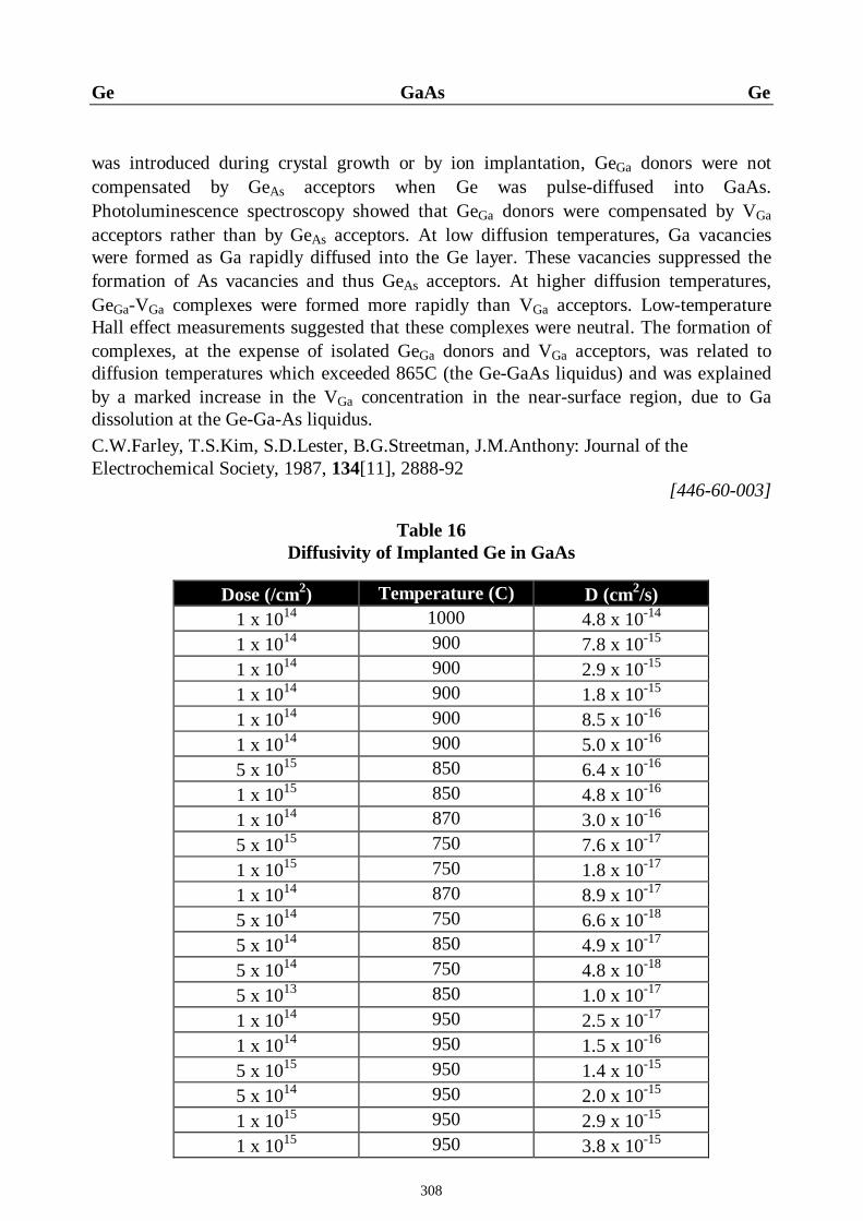
308
Ge GaAs Ge
was introduced during crystal growth or by ion implantation, GeGa donors were notcompensated by GeAs acceptors when Ge was pulse-diffused into GaAs.Photoluminescence spectroscopy showed that GeGa donors were compensated by VGa
acceptors rather than by GeAs acceptors. At low diffusion temperatures, Ga vacancieswere formed as Ga rapidly diffused into the Ge layer. These vacancies suppressed theformation of As vacancies and thus GeAs acceptors. At higher diffusion temperatures,GeGa-VGa complexes were formed more rapidly than VGa acceptors. Low-temperatureHall effect measurements suggested that these complexes were neutral. The formation ofcomplexes, at the expense of isolated GeGa donors and VGa acceptors, was related todiffusion temperatures which exceeded 865C (the Ge-GaAs liquidus) and was explainedby a marked increase in the VGa concentration in the near-surface region, due to Gadissolution at the Ge-Ga-As liquidus.C.W.Farley, T.S.Kim, S.D.Lester, B.G.Streetman, J.M.Anthony: Journal of theElectrochemical Society, 1987, 134[11], 2888-92
[446-60-003]
Table 16Diffusivity of Implanted Ge in GaAs
Dose (/cm2) Temperature (C) D (cm2/s)1 x 1014 1000 4.8 x 10⁻¹⁴
1 x 10¹⁴ 900 7.8 x 10⁻¹⁵
1 x 10¹⁴ 900 2.9 x 10⁻¹⁵
1 x 10¹⁴ 900 1.8 x 10⁻¹⁵
1 x 10¹⁴ 900 8.5 x 10⁻¹⁶
1 x 10¹⁴ 900 5.0 x 10⁻¹⁶
5 x 10¹⁵ 850 6.4 x 10⁻¹⁶
1 x 10¹⁵ 850 4.8 x 10⁻¹⁶
1 x 10¹⁴ 870 3.0 x 10⁻¹⁶
5 x 10¹⁵ 750 7.6 x 10⁻¹⁷
1 x 10¹⁵ 750 1.8 x 10⁻¹⁷
1 x 10¹⁴ 870 8.9 x 10⁻¹⁷
5 x 10¹⁴ 750 6.6 x 10⁻¹⁸
5 x 10¹⁴ 850 4.9 x 10⁻¹⁷
5 x 10¹⁴ 750 4.8 x 10⁻¹⁸
5 x 10¹³ 850 1.0 x 10⁻¹⁷
1 x 10¹⁴ 950 2.5 x 10⁻¹⁷
1 x 10¹⁴ 950 1.5 x 10⁻¹⁶
5 x 10¹⁵ 950 1.4 x 10⁻¹⁵
5 x 10¹⁴ 950 2.0 x 10⁻¹⁵
1 x 10¹⁵ 950 2.9 x 10⁻¹⁵
1 x 10¹⁵ 950 3.8 x 10⁻¹⁵

309
Ge GaAs H
GaAs: Ge DiffusionImplantation (3 x 10¹³/cm2) of 200keV Ge into (x11)A-oriented semi-insulating GaAssubstrates (where x took values of up to 4) was carried out. For comparison, (110)- and(100)-oriented substrates were also implanted. No in-diffusion of Ge was observed afterannealing substrates of any orientation.M.V.Rao, H.B.Dietrich, P.B.Klein, A.Fathimulla, D.S.Simons, P.H.Chi: Journal ofApplied Physics, 1994, 75[12], 7774-8
[446-117/118-166]
Figure 5: Diffusivity of H in GaAs
H
317 GaAs: H DiffusionIt was recalled that the diffusion of neutral H atoms into a semiconductor wasaccompanied by their binding into molecules. When the thermal dissociation of moleculescould be ignored, and for times which were sufficiently long to establish an equilibrium
1.0E-13
1.0E-12
1.0E-11
1.0E-10
1.0E-09
1.0E-08
1.0E-07
13 14 15 16 17 18 19 20
table 17table 18
104/T(K)
D (c
m2 /s
)

310
H GaAs H
state for the binding of H into complexes with impurity atoms, the formation of moleculeswas the main process which determined the steady-state profile of atomic H whichformed near to the crystal surface. By analyzing secondary ion mass spectrometry data interms of a model for this process, it was estimated that the diffusivity of H was equal to1.4 x 10-10 cm2/s at 360C and equal to 5.5 x 10⁻¹¹cm2/s at 390C. When combined withanother result, it was deduced that the overall data (table 17) could be described by:
D (cm2/s) = 0.0385 exp[-1.13(eV)/kT]N.S.Rytova: Fizika i Tekhnika Poluprovodnikov, 1991, 25[6], 1078-80 (Soviet Physics -Semiconductors, 1991, 25[6], 650-1)
Table 17Diffusivity of H in GaAs
Temperature (C) D (cm2/s)390 5.2 x 10⁻¹¹
360 1.2 x 10⁻¹⁰
250 1.0 x 10⁻¹²
GaAs: H DiffusionLayers of material, which was doped with various group-VI donors (S, Se, Te), wereexposed to H plasma. Electronic measurements indicated that, after H diffusion, theelectron concentration systematically decreased while their mobility increased; thusdemonstrating the passivation of the group-VI donors by H.B.Theys, B.Machayekhi, J.Chevallier, K.Somogyi, K.Zahraman, P.Gibart, M.Miloche:Journal of Applied Physics, 1995, 77[7], 3186-93
[446-121/122-052]
GaAs: H DiffusionThe ability of charged H to drift in this material was used to investigate the behavior ofH. It was concluded that diffusion within the above temperature range was entirely trap-limited, and exhibited no dependence upon the diffusivity of free H. By drifting H awayfrom the donors in hydrogenated n-type GaAs, reactivation of the passivated donors couldbe studied. Thermal dissociation of the donor-H complex obeyed first-order kinetics, witha dissociation energy of 1.52eV.A.W.R.Leitch, T.Zundel, T.Prescha, J.Weber: Materials Science Forum, 1992, 83-87, 21-6
[446-93/94-009]
GaAs: H DiffusionFirst-principles calculations were made of the properties of atomic and molecular H inpure bulk material. The results indicated that the H penetrated in atomic form. Within thesample, atomic H tended to form H2 molecules on tetrahedral sites. These were deepenergy wells for H2. The H2* defect, which consisted of a H atom in a bond-center site

311
H GaAs H
and a H atom in an adjacent tetrahedral position, had a higher energy than H2 but was alower-energy barrier to diffusion. Isolated H could be present as a metastable species.The stable charge state of isolated H was calculated as a function of the Fermi energy.The results suggested that H behaved as a negative-U defect. Consequently, isolated Hwas expected to be present only as a charged species (positively charged in p-dopedsamples, negatively charged in undoped and n-doped samples). The conclusions werecompared with experimental results and with the results of calculations for H in othersemiconductors. The main features of H behavior in GaAs were quite similar to those forSi.L.Pavesi, P.Giannozzi: Physical Review B, 1992, 46[8], 4621-9
[446-93/94-009]
GaAs: H DiffusionIt was pointed out that Se donors in n-type material were passivated by exposure to a Hplasma. Thermal reactivation of the passivated donors was investigated at temperaturesranging from 154 to 191C. By using the electric field of a reverse-biased Schottky diodestructure, the drift of thermally dissociated H as a negatively charged species wasdemonstrated. The thermal dissociation of the SeH complex obeyed first-order kinetics,with a dissociation energy of 1.52eV.A.W.R.Leitch, T.Prescha, J.Weber: Physical Review B, 1991, 44[3], 1375-8
[446-84/85-016]
GaAs: H DiffusionIt was shown that the exponential depth profiles which were sometimes observed duringH diffusion into semiconductors, such as Si and GaAs, could be explained by including aterm (in the diffusion equation) that described the multiple trapping of H at an impurity. Itwas shown that the effective dimensionality of the random walk in the present case wasinfinite.D.A.Tulchinsky, J.W.Corbett, J.T.Borenstein, S.J.Pearton: Physical Review B, 1990,42[18], 11881-3
[446-81/82-010]
GaAs: H DiffusionThe concentration versus depth profiles of carriers, electrically active defects, and D,after exposure to a H plasma (or molecular H), were fitted by using a simple diffusionmodel which involved second-order reactions. It was found that the activation energy forH diffusion, and the dissociation energies of H-defect complexes, depended upon the Hconcentration. There was no molecular H formation and there were no fast-diffusing Hspecies away from the near-surface region. Atomic H could in-diffuse and passivate EL2defects when semi-insulating material was annealed at a high temperature in a molecularH ambient.R.A.Morrow: Journal of Applied Physics, 1989, 66[7], 2973-9
[446-74-010]

312
H GaAs H
GaAs: H DiffusionWafers of n-type material were exposed to a capacitively coupled radio-frequency Hplasma, with power densities of between 0.01 and 0.2W/cm2 at 260C. The properties ofthe layers were investigated by using deep-level transient spectroscopy and capacitance-voltage methods. As well as the neutralization of Si donors by in-diffused H atoms, it wasfound that there was a modification of the deep-level transient spectroscopy spectra afterhydrogenation. At two radio-frequency power densities of less than 0.IW/cm2, deep levelsin the original material were passivated. The results also indicated that the complexeswhich were present were either electrically inactive or were located deep within theenergy band-gap. At power densities of more than 0.1W/cm2, two new deep statesappeared at 0.41 and 0.55eV below the conduction band. These levels were attributed to alarge number of defects which were situated in the near-surface region of n-type Si-dopedmaterial after H plasma exposure. It was suggested that the trapping of H at these defectswas probably responsible for the observed accumulation of H in the near-surface region.A.Jalil, A.Heurtel, Y.Marfaing, J.Chevallier: Journal of Applied Physics, 1989, 66[12],5854-61
[446-74-010]
GaAs: H DiffusionThe depth profiles of 60 and 100keV protons which were implanted to fluences of 1016 or1017/cm2 at room temperature were determined by using ion beam techniques. The Hprofiles were measured as a function of annealing temperatures of up to 820K. It wasfound that the redistribution of implanted H depended upon the migration ofimplantation-induced defects. The migration of H-defect complexes was described by theexpression:
D(cm2/s) = 2 x 10⁵ exp[-2.16(eV)/kT]J.Räisänen, J.Keinonen, V.Karttunen, I.Koponen: Journal of Applied Physics, 1988,64[5], 2334-6
[446-72/73-010]
318 GaAs: H DiffusionProfiles which reflected the passivation of electrically active and recombination-activecenters by atomic H in single crystals were investigated by using secondary ion massspectrometry and microcathodoluminescence methods. The former data indicated that theprofiles were the same for all of the samples, and consisted of an 0.0005mm surfaceregion with a H content of 1020/cm3 and a low diffusion rate. This was followed by adiffusion tail with a much higher diffusion rate. In this tail region, the activation energyfor H diffusion was 0.83eV at temperatures of between 200 and 500C (table 18), and thediffusivity was 6.7 x 10⁻⁹cm2/s at 400C. It was proposed that the results confirmed thesuggested migration of neutral interstitial H. The introduction of atomic H completelysuppressed a microcathodoluminescence inhomogeneity which was associated withdislocations in the semi-insulating material.

313
H GaAs H
E.M.Omelyanovskii, A.V.Pakhomov, A.J.Polyakov, A.V.Govorkov, O.M.Borodina,A.S.Bruk: Fizika i Tekhnika Poluprovodnikov, 1988, 22[7], 1203-7. (Soviet Physics -Semiconductors, 1988, 22[7], 763-5)
[446-62/63-210]
Table 18Diffusivity of H in GaAs
Temperature (C) D (cm2/s)480 2.3 x 10⁻⁸
425 5.1 x 10⁻⁸
445 1.4 x 10⁻⁸
445 1.0 x 10⁻⁸
420 1.2 x 10⁻⁸
410 7.7 x 10⁻⁹
410 6.2 x 10⁻⁹
390 2.2 x 10⁻⁹
365 2.8 x 10⁻⁹
365 1.9 x 10⁻⁹
320 2.2 x 10⁻⁹
320 9.4 x 10⁻¹⁰
290 6.0 x 10⁻¹⁰
295 2.7 x 10⁻¹⁰
255 2.3 x 10⁻¹⁰
255 1.3 x 10⁻¹⁰
GaAs: H DiffusionExperiments were performed on buried Si-doped epilayers under hydrostatic pressure. Itwas found that the D diffusion profile in n-type Si-doped samples depended upon thehydrostatic pressure, and consisted of a plateau that was followed by a steep progressivedecrease as the pressure was increased. This was explained as being due to an increasingimportance of the trapping-detrapping process of H- on Si+ donors during H diffusion.This increase was attributed to a deepening of the H acceptor level, with respect to thebottom of the Γ conduction band, as the hydrostatic pressure was increased.D.Machayekhi, J.Chevallier, B.Theys, J.M.Besson, G.Weill, G.Syfosse: Solid StateCommunications, 1996, 100[12], 821-4
[446-141/142-098]
GaAs: H DiffusionThe results of investigations of transitions among the sites and charge states of muoniumwere summarized. A model was developed which accounted for all of the major features

314
H GaAs H
which were observed. Its validity for a wide range of dopant concentrations, using asingle set of parameters, reflected its predictive strength. The near equality of the energyparameters for muonium, as compared with those which were available for H, stronglyimplied that the results for muonium dynamic behavior should be applicable to H, withvery little change. The model could be applied to all tetrahedrally coordinatedsemiconductors, with few modifications, and served as a basis for the understanding ofmuonium dynamics and therefore for the behavior of H in GaAs and other materials.Differences in H properties could be understood by examining material-specificdeviations from the basic model.R.L.Lichti, C.Schwab, T.L.Estle: Materials Science Forum, 1995, 196-201, 831-6
[446-127/128-119]
GaAs: H DiffusionThe diffusivity of H+ was directly determined by means of capacitance transientmeasurements. The H was released from donor-H complexes, in the space-charge layer ofSchottky diodes on n-type material, by the pulsed-laser injection of minority carriers.Capacitance-voltage measurements revealed a recovery of donor dopants after injection.This demonstrated minority-carrier enhanced dissociation of a donor-H complex.Capacitance transients which were recorded during the migration of H+ were analyzed inorder to obtain diffusivities at near to room temperature. At 320K, the diffusivity wasequal to 10-12cm2/s, to within a factor of 2. An Arrhenius plot of the migration time-constant yielded an activation energy for H+ diffusion of about 0.66eV.N.M.Johnson, C.Herring, D.Bour: Physical Review B, 1993, 48[24], 18308-11
[446-115/116-117]
GaAs: H DiffusionDiffusion experiments were performed on samples of Si-doped AlxGa1-xAs epitaxiallayers, with x-values which ranged from 0 to 0.30, as a function of the Si doping leveland the diffusion temperature. For each composition, calculated H diffusion profileswhich had been deduced by using Mathiot's model were fitted to the experimentalprofiles. It was assumed that H behaved as a deep acceptor, and that Ho and H- were thediffusing species. The trapping of H- by Si+ donors, and their acceleration by an electricfield, were incorporated into the model. As well as the diffusion coefficient of H, and thedissociation constant of the SiH complexes, the model provided for a compositionaldependence of the H acceptor level in AlGaAs alloys. Extrapolation of the H acceptorlevel to x = 0 gave its value for GaAs. This level was located at 0.10eV below the Γconduction band of GaAs.B.Machayekhi, R.Rahbi, B.Theys, M.Miloche, J.Chevallier: Materials Science Forum,1994, 143-147, 951-6
[446-113/114-001]
GaAs: H DiffusionThe depth profiles of diffused H in n-type samples were determined by means ofsecondary ion mass spectroscopy. Specimens with Si donor concentrations which ranged
315
H GaAs In
from 1017 to 5 x 10¹⁸/cm3 were exposed to monatomic D from a remote microwaveplasma at temperatures of between 250 and 310C. The profiles clearly revealed that Daccumulation occurred up to a concentration that was almost equal to that of the donorsover a depth which depended upon the temperature and time of hydrogenation and uponthe donor concentration. A plateau in the H concentration was attributed to a trapping-limited migration of H which was dominated by the formation of SiH complexes via theCoulombic attraction of Si+ and H-. The analysis of profiles in the tail region beyond theplateau yielded independent estimates of the thermal dissociation rate for the SiHcomplex, and a lower limit of about 0.45eV for the binding of Si+ and H- into SiH.G.Roos, N.M.Johnson, C.Herring, J.Walker: Materials Science Forum, 1994, 143-147,933-8
[446-113/114-011]
In
GaAs: In DiffusionAn InAs monolayer was grown between GaAs layers by using the migration-enhancedepitaxy method. The surface chemical characteristics during growth were investigated bymeans of reflection high-energy electron diffraction. When the substrate temperature wasequal to about 500C, the oscillation amplitude of the reflected electron beam after thegrowth of one monolayer of InAs vanished during the growth of GaAs over more than 20atomic layers. High-resolution secondary ion mass spectroscopic analysis of thefabricated structures indicated that an anomalous distribution of In atoms, with a gradualslope towards the growth direction, occurred when the substrate temperature was 500C.The experimental results were explained in terms of the replacement of In atoms, in theInAs monolayer, by newly deposited Ga atoms.H.Yamaguchi, Y.Horikoshi: Japanese Journal of Applied Physics, 1989, 28[11], L2010-2
[446-72/73-011]
GaAs: In DiffusionThe diffusion of In markers at 900C was measured in undoped and Te-doped epilayerswhich had been prepared by using organometallic vapor-phase epitaxy. It was found thatthe diffusivity was a linear function of electron concentrations ranging from 2 x 10¹⁷ to1.5 x 1019/cm3. It was concluded that the results were consistent with the interdiffusion ofAlAs and GaAs superlattices. Also, the In and Al diffusivities at 900C were essentiallyidentical; within experimental error. The results strongly suggested that group-IIIinterdiffusion in this material was controlled by a Ga vacancy with a charge of -1.W.M.Li, R.M.Cohen, D.S.Simons, P.H.Chi: Applied Physics Letters, 1997, 70[25], 3392-4
[446-152-0315]

316
In GaAs Li
GaAs/InAs: In DiffusionThe segregation and interdiffusion of In atoms in GaAs/InAs/GaAs heterostructures wereinvestigated by using secondary ion mass spectroscopy. When the InAs was grown in thelayer-by-layer growth mode, with no dislocations, the segregation of In atoms becamemarked with increasing growth temperature. However, segregation was observed even atthe relatively low growth temperature of 400C during molecular beam epitaxy. It wasfound that segregation was markedly enhanced by dislocations which were near to thehetero-interface when thick InAs layers were grown in a 3-dimensional island growthmanner. Interdiffusion of In atoms towards the growth direction occurred after thermalannealing, and could be assisted by vacancies which propagated from the film surface andinto the epilayer. It became apparent that interdiffusion was effectively suppressed byinserting a thin AlAs layer into the GaAs cap layer.T.Kawai, H.Yonezu, Y.Ogasawara, D.Saito, K.Pak: Journal of Applied Physics, 1993,74[3], 1770-5
[446-106/107-085]
GaAs/Si: In DiffusionSamples of GaAs, which were encapsulated with thin films of amorphous Si at 450C,were annealed at temperatures of up to 1050C. The resultant poly-Si/GaAs interfaceswere investigated by using secondary ion mass spectroscopy, Rutherford back-scatteringspectrometry, and transmission electron microscopy. Little or no interdiffusion wasdetected at undoped Si/GaAs interfaces. The diffusion of dopants such as InP wasdetected. An enhanced diffusivity of In into GaAs was attributed to the diffusion of pointdefects which were created by the diffusion of As and Ga into the encapsulant. It wasdeduced that the In diffusivities in GaAs at doped polycrystalline Si interfaces wereenhanced by factors of about 10000.K.L.Kavanagh, C.W.Magee, J.Sheets, J.W.Meyer: Journal of Applied Physics, 1988,64[4], 1845-54
[446-72/73-027]
Li
GaAs: Li DiffusionStrong photoluminescence bands, at 1.34 and 1.45eV, were observed after the Lidiffusion of various samples of n-type material at temperatures of between 400 and 600C.The photoluminescence bands were homogeneous throughout the bulk of the samples.They were never observed in originally p-type or semi-insulating material. A hole at Ev +0.17eV was detected by means of deep-level transient spectroscopic measurements, andan acceptor level at Ev + 0.14eV was revealed by temperature-dependent Hallmeasurements of n-type material which had been converted to p-type by Li diffusion. It

317
Li GaAs Mg
was suggested that LiGa-D acceptors were connected with compensation andphotoluminescence bands.B.H.Yang, T.Egilsson, S.Kristjánsson, J.Pétursson, H.P.Gislason: Materials ScienceForum, 1994, 143-147, 839-44
[446-113/114-012]
GaAs: Li DiffusionThe correlation between the electrical conductivity and photoluminescence spectra of awide range of n-type, p-type, and semi-insulating material which had been diffused withLi was investigated. It was found that Li diffusion compensated both n-type and p-typematerial, and had a marked effect upon the photoluminescence properties of the samples.The photoluminescence bands which were observed, between 1.47 and 1.49eV in Zn-doped GaAs, were related to the compensation of Zn acceptors. The photoluminescencebands, which were observed at 1.43 to 1.45eV in all of the samples, were attributed to aLi-related acceptor complex which gave rise to the p-type conductivity which wasobserved in all of the samples after full compensation.H.P.Gislason, B.Yang, I.S.Haukson, J.T.Gudmundsson, M.Linnarsson, E.Janzén:Materials Science Forum, 1992, 83-87, 985-90
[446-99/100-064]
Mg
GaAs: Mg DiffusionThe migration of thin highly p-doped layers in single and double heterostructures, grownusing metalorganic vapor-phase epitaxy, was studied by using capacitance-voltage etchprofiling and secondary ion mass spectrometry. It was deduced that the diffusivity of Mgin GaAs could be described by:
D (cm2/s) = 6.5 x 10⁻⁵ exp[-1.8(eV)/kT]for rapid thermal annealing, while the diffusivity could be described by:
D (cm2/s) = 1.9 x 10⁻⁷ exp[-1.5(eV)/kT]for furnace annealing. A model which was based upon an interstitial cum substitutionaldiffusion mechanism, with certain kinetic limitations, was successfully used to simulatethe observed dopant concentration profiles.N.Nordell, P.Ojala, W.H.Van Berlo, G.Landgren, M.K.Linnarsson: Journal of AppliedPhysics, 1990, 67[2], 778-86
[446-74-004]
GaAs: Mg DiffusionThe transient up-hill diffusion of Mg during annealing at 900C was computer-simulated.It was assumed that diffusion occurred via the substitutional-interstitial mechanism, withexcess interstitials and vacancies being produced by implantation; thus causing theabnormal diffusion behavior. The substitutional-interstitial mechanism was shown to bemathematically equivalent to an existing interstitial-dopant pair diffusion model. This

318
Mg GaAs Mg
permitted the programme (a Si process simulator that included dopant/point-defectinteractions) to be used to model up-hill diffusion if suitable diffusivity and defectparameters were included. The profiles of excess interstitials and vacancies which wereproduced by the implantation process were deduced from Boltzmann transport equationcalculations. It was found that transient up-hill diffusion could be accurately simulated;with the dopant diffusing, from regions with excess interstitials, towards the surface ortowards regions with excess vacancies. When the defect concentrations had returned totheir steady-state levels, via diffusion, recombination, or capture by sinks, normalconcentration-dependent diffusion into the substrate occurred.H.G.Robinson, M.D.Deal, G.Amaratunga. P.B.Griffin, D.A.Stevenson, J.D.Plummer:Journal of Applied Physics, 1992, 71[6], 2615-23
[446-86/87-010]
GaAs: Mg DiffusionIt was noted that Mg implants in this material exhibited 2 types of diffusion duringannealing. These were up-hill diffusion in the implantation peak, and concentration-dependent diffusion into the bulk. The up-hill diffusion predominated at short times andlow temperatures, while the concentration-dependent diffusion was predominant at longtimes and high temperatures. By studying implants that had been annealed at temperatureswhere no up-hill diffusion occurred, diffused profiles could be modelled and anexpression for the Mg diffusivity could be obtained. The activation energy for thisprocess was 1.77eV. The results of Fermi level experiments showed that the diffusivitywas hole-dependent rather than concentration dependent. The hole-dependent exponentwas equal to unity for Mg which was implanted into semi-insulating substrates, but couldchange to 2 at high hole concentrations.H.G.Robinson, M.D.Deal, D.A.Stevenson: Applied Physics Letters, 1991, 58[24], 2800-2
[446-81/82-010]
GaAs: Mg DiffusionThe redistribution of Mg implants during post-implantation annealing was studied inorder to evaluate the effect of implantation damage upon the diffusion process. Rapid up-hill diffusion was observed in the peak of Mg implants. This was explained by invoking asubstitutional-interstitial diffusion mechanism and by performing computer simulations ofdamage-generated point defects. In the up-hill diffusion region, the dopants diffused fromareas of excess interstitial concentration towards areas of excess vacancy concentration.A critical point defect concentration was necessary in order to initiate up-hill diffusion.H.G.Robinson, M.D.Deal, D.A.Stevenson: Applied Physics Letters, 1990, 56[6], 554-6
[446-74-009]
GaAs: Mg DiffusionUn-capped wafers were annealed in an AsH3-N2 atmosphere for 10s, at temperatures ofup to 1100C. No surface decomposition occurred under an AsH3 partial pressure of12.5torr. The present method was used to activate implanted Mg. Measurements of thesheet resistance of the annealed layers, as a function of the annealing temperature,

319
Mg GaAs Mn
revealed a minimum at a temperature of about 930C. At higher temperatures, thediffusion of Mg became significant. Part of the Mg accumulated at the surface anddiffused out. The internal diffusion of Mg at high temperatures depended upon the AsH3pressure during annealing.H.Tews, R.Neumann, A.Hoepfner, S.Gisdakis: Journal of Applied Physics, 1990, 67[6],2857-61
[446-74-010]
GaAs: Mg DiffusionThe surface of material which had been implanted with Mg ions (100keV, 1015/cm2) wasencapsulated with As-doped amorphous hydrogenated Si to a thickness of about 80nm. Itwas found that the sheet carrier concentration in thermally annealed samples increasedwith increasing concentration of As in the encapsulant. After annealing (800C, 0.25h), asheet carrier concentration of about 3 x 10¹⁴/cm2 was observed in samples which werecapped with films that were doped with 2 x 10²⁰/cm3 of As. It was noted that thediffusivity of the implanted Mg was retarded upon increasing the concentration of As inthe amorphous hydrogenated Si encapsulant.K.Yokota, M.Sakaguchi, H.Inohara, H.Nakanishi, S.Tamura, Y.Horino, A.Chayahara,M.Satho, K.Hira, H.Takano, M.Kumagaya: Solid-State Electronics, 1994, 37[1], 9-15
[446-113/114-012]
Mn
GaAs: Mn DiffusionThe diffusion of Mn was carried out in sealed quartz ampoules, using 4 types of Mnsource. These were: solid crystalline Mn grains, Mn3As, MnAs, and Mn thin films onGaAs substrates. It was found that only MnAs led to the formation of a smooth GaAssurface and a uniform dopant distribution. In the case of the other sources, interactionsbetween the source materials and the substrate gave rise to poor surface morphologies andinhomogeneous distributions. In the case of diffusion at 800C, surface p-type carrierconcentrations of the order of 1020/cm3 were obtained. The diffusion profiles which weredetermined by using capacitance-voltage techniques resembled those which wereobtained for Zn diffusion. It was suggested that a substitutional-interstitial mechanismwas the predominant one.C.H.Wu, K.C.Hsieh, G.E.Höfler, N.El-Zein, N.Holonyak: Applied Physics Letters, 1991,59[10], 1224-6
[446-84/85-007]
GaAs: Mn DiffusionPlates of Sn-doped n-type material were coated with 54Mn, annealed (1100C, 4h) andanalyzed by using alternate grinding and activity measurements. The diffusion profilescould be described by an erfc function, and the diffusivity at the annealing temperaturewas estimated to be 4.3 x 10⁻¹⁰cm2/s.
320
Mn GaAs Ni
E.A.Skoryatina, R.S.Malkovich: Fizika i Tekhnika Poluprovodnikov, 1989, 23[1], 164-6.(Soviet Physics - Semiconductors, 1989, 23[1], 101-2)
[446-70/71-106]
GaAs: Mn DiffusionIt was pointed out that one of the potential advantages of rapid thermal annealing, ascompared with conventional furnace annealing, was a reduced implanted dopant andbackground impurity diffusion. Here, the migration of Mn during the annealing of Cr-doped semi-insulating material implanted with 100keV Si+ ions to a dose of 7 x 10¹²/cm2
was measured by using secondary ion mass spectrometry. Un-capped rapid thermalannealing (860 or 930C, 1 to 60s) was investigated and its effect was compared with thatof capless furnace annealing (0.5h). The migration of Mn was undetectable for rapidthermal annealing times which were shorter than 60s, but dominated 0.5h furnaceanneals.H.Kanber, J.M.Whelan: Journal of the Electrochemical Society, 1987, 134[10], 2596-9
[446-55/56-005]
GaAs: Mn DiffusionA study was made of the effect of an As over-pressure upon Mn diffusion. The sources ofMn included solid Mn thin films, which were deposited directly onto the GaAs substrate,and Mn vapor from pure solid Mn, MnAs, or Mn3As. When a solid Mn film was used asthe diffusion source, a non-uniform dopant distribution and a poor surface morphologywas obtained. This was due to reaction between the Mn film and the GaAs matrix. Thedegraded surface consisted of a layer of polycrystalline cubic alloy with a lattice constantof almost 0.84nm, and with a composition that was close to Ga2Mn; with a small amountof As. Of the remaining diffusion sources, only MnAs consistently produced a uniformdoping distribution and a smooth surface morphology. By diffusion at 800C, a uniformsurface hole carrier concentration as high as 1020/cm3 could be obtained by using MnAsas a source. The As over-pressure was found to alter drastically the Mn diffusion profileand Mn, like Zn, could diffuse interstitial-substitutionally. Vapor from Mn or Mn3Asdegraded the surface. However, Mn3As degraded the surface more rapidly. A sufficientlyhigh As over-pressure completely suppressed surface degradation.C.H.Wu, K.C.Hsieh: Journal of Applied Physics, 1992, 72[12], 5642-8
[446-106/107-037]
Ni
GaAs: Ni DiffusionThe redistribution of Ni in a Ni/GaAs contact specimen was studied by using neutronactivation and sectioning techniques at temperatures of between 360 and 870K. It wasconcluded that interdiffusion of the components took place in an elastic strain field whichwas generated by differences in the lattice parameters and thermal expansion coefficientsof Ni, GaAs and intermetallic compounds which formed. At annealing temperatures below570K, reactive diffusion of Ni took place, with an activation energy of 0.51eV. The
321
Ni GaAs O
formation of micro-cracks in the surface layers of the microcrystalline GaAs led todiffusion with an activation energy of 0.25eV. At annealing temperatures that weregreater than 670K the internal electric field, and cluster formation, markedly affected thedistribution of the components.W.A.Uskov, A.B.Fedotov, E.A.Erofeeva, A.I.Rodionov, D.T.Dzhumakulov: IzvestiyaAkademii Nauk SSSR - Neorganicheskie Materialy, 1987, 23[2], 186-9. (InorganicMaterials, 1987, 23[2], 163-5)
[446-55/56-006]
O
GaAs: O DiffusionA new technique was developed in order to study atomic movements during ultra-violetlaser-enhanced and low-temperature (below 400C) thermal oxidation. This methodcombined a classical marker technique with low-energy ion-scattering spectroscopy.During the formation of thin (about 1nm) oxide layers, the marker remained on the oxidesurface. This indicated that oxidation occurred, at the GaAs/oxide interface, via thediffusion of an O species. This differed from the oxidation of metals such as Ni and Cu,where the use of the same technique confirmed earlier observations that oxidationoccurred at the oxide/ambient interface. The diffusion of a metal species resulted in themarker being buried during oxidation of the metal surfaces.M.T.Schmidt, Z.Wu, C.F.Yu, R.M.Osgood: Surface Science, 1990, 226[1-2], 199-205
[446-74-011]
GaAs: O DiffusionThe thermal surface oxidation of samples in dry O2 and in ambient air was investigated attemperatures ranging from 400 to 530C. The studies were carried out by using cleanpolished (111) substrates. It was found that monocrystalline wafers oxidized parabolicallyin dry O2 at temperatures of 400 to 450C. Linear oxide growth occurred, at temperaturesranging from 480 to 530C, in both in dry O2 and in ambient air. Wagner and Grimley-Trapnell models for metal oxidation were used to identify the growth kinetics. The rateconstants for parabolic and linear oxidation were temperature-dependent, and satisfiedArrhenius relationships.J.Kucera, K.Navratil: Thin Solid Films, 1990, 191[2], 211-20
[446-78/79-012]
GaAs: O DiffusionPublished depth profiles of D in n-type and p-type material, after extended annealing in Dat 500C, were suggested to reflect the in-diffusion of a native defect (perhaps VAs) and animpurity (perhaps O); both of which were tagged with D. It was deduced that thediffusivity of the tagged impurity was equal to 4 x 10-14cm2/s at 500C. The diffusivity of

322
O GaAs S
the tagged native defect was deduced to be equal to 3 x 10-15cm2/s in n-type material, andto be equal to about 8 x 10-15cm2/s in p-type material.R.A.Morrow: Applied Physics Letters, 1990, 57[3], 276-8
[446-76/77-009]
GaAs: O DiffusionInfra-red measurements of the concentrations of H-B pairs, which formed in B-doped Sithat had been heated in H2 gas and quenched from temperatures of between 900 and1300C, led to a new determination of the H solubility:
[H](/cm3) =9.1 x 10²¹ exp[-1.80(eV)/kT]There was some evidence that H2 molecules also formed. The presence of H led to anenhancement of the diffusivity of O impurities at temperatures below 500C. Suggestionsthat H was present in as-grown Czochralski Si were supported by the observation of H-Ccomplexes, using photoluminescence techniques. The analysis of the structure of a Hcomplex, by means of infra-red vibrational spectroscopy, was illustrated for the case ofthe H-CAs pair in GaAs.R.C.Newman: Philosophical Transactions of the Royal Society A, 1995, 350[1693], 215-26
[446-119/120-192]
P
GaAs/Si: P DiffusionSamples of GaAs, which were encapsulated with thin films of amorphous Si at 450C,were annealed at temperatures of up to 1050C. The resultant poly-Si/GaAs interfaceswere investigated by using secondary ion mass spectroscopy, Rutherford back-scatteringspectrometry, and transmission electron microscopy. Little or no interdiffusion wasdetected at undoped Si/GaAs interfaces. The diffusion of dopants such P was detected.An enhanced diffusivity of P into GaAs was attributed to the diffusion of point defectswhich were created by the diffusion of As and Ga into the encapsulant. It was deducedthat the P diffusivities in GaAs at doped polycrystalline Si interfaces were enhanced byfactors of about 10000.K.L.Kavanagh, C.W.Magee, J.Sheets, J.W.Meyer: Journal of Applied Physics, 1988,64[4], 1845-54
[446-72/73-027]
S
GaAs: S DiffusionExperiments were performed on polished plates of Te-doped material. Irradiation with 15to 150keV protons was carried out at 300K to doses of between 1016 and 1017/cm2. It wasfound that the impurity profiles did not depend upon whether the diffusion source was

323
S GaAs S
deposited before or after irradiation. The penetration depth in samples which wereirradiated with 15keV protons was greater than that in samples which were irradiated with150keV protons. It was suggested that this was because the low-energy ions generatedmore defects at depths of between 50 and 100nm.V.N.Abrosimova, V.V.Kozlovskii, N.N.Korobkov, V.N.Lomasov: Izvestiya AkademiiNauk SSSR - Neorganicheskie Materialy, 1990, 26[3], 488-91. (Inorganic Materials,1990, 26[3], 411-4)
[446-84/85-013]
Table 19Diffusivity of Implanted S in GaAs
120keV S+ (/cm2) Temperature (C) D (cm2/s)1 x 1015 1000 1.4 x 10⁻¹²
1 x 10¹⁵ 950 9.6 x 10⁻¹³
1 x 10¹⁵ 900 7.1 x 10⁻¹³
1 x 10¹⁵ 850 5.4 x 10⁻¹³
5 x 10¹⁴ 1000 9.9 x 10⁻¹³
5 x 10¹⁴ 950 7.9 x 10⁻¹³
5 x 10¹⁴ 900 4.9 x 10⁻¹³
5 x 10¹⁴ 850 3.0 x 10⁻¹³
1 x 10¹⁴ 1000 5.0 x 10⁻¹³
1 x 10¹⁴ 950 3.4 x 10⁻¹³
1 x 10¹⁴ 900 1.3 x 10⁻¹³
5 x 10¹³ 1000 2.6 x 10⁻¹³
5 x 10¹³ 950 1.4 x 10⁻¹³
319,20 GaAs: S DiffusionSamples were implanted with 120keV S+ ions to doses of between 3 x 10¹³ and 1015/cm2
(table 19). They were capped with an 80nm-thick film of amorphous hydrogenated Si,into which As was doped to a concentration of 2 x 10²⁰/cm3. The samples were thenannealed in Ar gas (850 to 1000C, 0.25h). It was found that the diffusivity of S (table 20)could be described by the expression:
D = Dm[KQ2/(1 + KQ2)]where K was a constant, Q was the implantation dose, and Dm was the diffusivity of amobile complex.M.Sakaguchi, K.Yokota, A.Shiomi, K.Hirai, H.Takano, M.Kumagai: Japanese Journal ofApplied Physics, 1996, 35[1-8], 4203-8
[446-138/139-077]
324
S GaAs S
GaAs: S DiffusionSamples were implanted with 500keV S ions, through 120nm-thick films of amorphoushydrogenated Si, to give a concentration of 2 x 10²⁰/cm3. They were then annealed (700to 1000C, 0.25h, Ar). It was found that the diffusivity of the S decreased with increasingimplantation dose.M.Sakaguchi, K.Yokota, A.Shiomi, H.Mori, A.Chayahara, Y.Fujii, K.Hirai, H.Takano,M.Kumagai: Japanese Journal of Applied Physics, 1996, 35[1-3], 1624-9
[446-136/137-110]
Table 20Diffusion Parameters for Implanted S in GaAs
Dose (/cm2) Do (cm2/s) E (eV)1 x 10¹⁵ 2.0 x 10⁻⁹ 0.85 x 10¹⁴ 9.0 x 10⁻⁹ 1.01 x 10¹⁴ 4.2 x 10⁻⁷ 1.55 x 10¹³ 5.5 x 10⁻⁷ 1.6
GaAs: S DiffusionAn investigation was made of the composition and thermal stability of ultra-violet, ozone-oxidized, and P2S5/(NH4)2S-treated (100) surfaces. In particular, X-ray photo-electronspectroscopy and Auger electron spectroscopy were used to probe the oxide and interfaceat room temperature and after annealing at various temperatures. The room temperaturedata indicated that S was buried between the oxide over-layer and the GaAs substrate.This oxide contained various As and Ga bonding configurations which, after moderateannealing, were transformed into more thermally stable phases, such as As2O3 and Ga2O3.Complete desorption of the oxide occurred after annealing at 600C. Heating the sample to495C caused some S to diffuse towards the oxide surface, while annealing at highertemperatures led to S diffusion into the GaAs substrate. Even after complete desorption ofthe O, a small amount of S remained in the GaAs lattice.M.J.Chester, T.Jach, J.A.Dagata: Journal of Vacuum Science and Technology A, 1993,11[3], 474-80
[446-111/112-050]
GaAs/Si: S DiffusionThe depth distribution of S near to a Si/GaAs(110) interface was measured by usingparticle-induced X-ray emission techniques, together with Rutherford back-scatteringspectrometry. Ozone oxidation and HF etching were used to remove layers. Themeasurements revealed the presence of a half-monolayer of S on H2Sx-passivated GaAs(110) surfaces. Upon depositing 1.5nm of Si onto S-passivated GaAs (110), the totalamount of S was found to remain constant as compared to that before Si deposition.

325
S GaAs Si
However, no oriented S-Ga bonds were revealed by X-ray absorption measurements, andthe depth profiles revealed that S atoms diffused into both the GaAs substrate and the Sihetero-layer.H.Xia, W.N.Lennard, L.J.Huang, W.M.Lau, J.M.Baribeau, D.Landheer: Journal ofApplied Physics, 1996, 80[8], 4354-7
[446-138/139-130]
Se
GaAs/Si: Se DiffusionThe surface of material which had been implanted with 100keV Se ions was encapsulatedwith As-doped amorphous hydrogenated Si to a thickness of about 80nm. Crystallizationof the encapsulant upon annealing at 1000C was hindered by doping with As atoms to aconcentration of 2 x10²⁰/cm3. However, the encapsulant could be crystallized when theconcentration of the As dopant atoms was lowered. The crystallized encapsulant hadmany grain boundaries, and the diffusion rate of impurities was thereby increased. TheGaAs surface decomposed markedly via the boundary of the Si/GaAs structure, and Asand Ga vacancies were produced at the GaAs surface. A number of Si atoms also diffusedinto the GaAs crystal. An As-vacancy rich region formed near to the surface, and the Gavacancy diffused into the GaAs because the diffusivity of the As vacancy in GaAs wasmuch lower than that of the Ga vacancy. The Si atoms gave a flat profile, with a steepslope at the surface, because of the distribution of the vacancies. That is, the Si atomspreferentially occupied vacant As sites in the VAs-rich region or vacant Ga sites in theVGa region. A series of reactions,
SeAs+ + (SiGa
+ + SiAs-) + VGa
- - (SeAs+ + SiAs
-) + (SiGa+ + VGa
-) →(SiAs
- + SeAs+) + (VGa
- + SiGa+)
increased the diffusion rate of the implanted Se atoms. Thus, the activation efficiencyimproved with increasing concentration of As atoms in the encapsulant, and the diffusionrate was reduced because the content of Si atoms and vacancies in GaAs was decreased.K.Yokota, K.Nishida, A.Yutani, S.Tamura, Y.Horino, A.Chayahara, M.Satho, K.Hirai,H.Takano, M.Kumagaya: Japanese Journal of Applied Physics, 1993, 32[1-10], 4418-24
[446-115/116-131]
Si
321 GaAs: Si DiffusionThe diffusion of Si was studied in <100> GaAs which had been implanted with 40keV30Si+ ions to a dose of 1016/cm2. The Si concentration profiles were determined by meansof secondary-ion mass spectrometry and nuclear resonance broadening techniques, andthe defect distributions were determined by using the Rutherford back-scatteringspectrometry channelling technique. The implanted samples were subjected to annealingin Ar at temperatures ranging from 650 to 850C (table 21). Two independent Si diffusion

326
Si GaAs Si
mechanisms were observed. It was found that concentration-independent diffusion, seenas a broadening of the initial implanted distribution, was very slow and was attributed toSi atoms that diffused interstitially. A concentration-dependent diffusivity with lowsolubility, which extended deeply into the sample, was quantitatively explained in termsof diffusion, via vacancies, of Si atoms on the Ga and As sub-lattices. Diffusioncoefficients, together with the carrier concentration as a function of Si concentration,were obtained at various temperatures. The concentration-independent diffusion of Si wasdescribed by:
D (cm2/s) = 1.23 x 10⁻⁷ exp[-1.72(eV)/kT]The solid solubility of Si in GaAs was determined, and an exponential temperaturedependence was observed. An estimate was made of the numbers of Si atoms whichresided on the Ga and As sites, and the number of SiGa
+-SiAs- pairs was deduced. The
intrinsic diffusivities via neutral Ga vacancy complexes, triply negatively charged Asvacancy complexes and triply negatively charged Ga vacancy complexes were:
D (cm2/s) = 3.74 x 10⁻³ exp[-2.60(eV)/kT]D (cm2/s) = 4.67 x 10⁻⁵ exp[-2.74(eV)/kT]
andD (cm2/s) = 5.92 x 10⁻⁸ exp[-2.28(eV)/kT]
respectively.T.Ahlgren, J.Likonen, J.Slotte, J.Räisänen, M.Rajatora, J.Keinonen: Physical Review B,1997, 56[8], 4597-603
[446-157/159-326]
GaAs: Si DiffusionThe d-doped samples were grown by using molecular beam epitaxial methods, and wereanalyzed by using high-resolution secondary ion mass spectrometry. It was found thatthere was a marked difference between the profiles which were produced from samplesthat had been doped to a surface density of less than 1.3 x 10¹³/cm2 (where all of the Siwas incorporated on Ga sites), and highly-doped samples (where auto-compensationoccurred). All of the samples were grown at a nominal temperature of 580C, and all ofthe doped planes showed some degree of broadening. A computer model for a 2-stepdiffusion process was developed, and this predicted a set of diffusion coefficients forlightly-doped samples. The diffusion coefficient which was associated with the post-deposition growth of these lightly-doped samples was about 4.2 x 10⁻¹⁷cm2/s. Because oftheir complicated profiles, more highly-doped samples were modelled by using agraphical technique. This revealed the presence of a much larger diffusion coefficient,which was tentatively attributed to the diffusion of Si as nearest-neighbor pairs.H.C.Nutt, R.S.Smith, M.Towers, P.K.Rees, D.J.James: Journal of Applied Physics, 1991,70[2], 821-6
[446-93/94-010]
GaAs: Si DiffusionTwo Si-doped specimens, which had been grown by using molecular beam epitaxytechniques, were used to study Si diffusion at temperatures ranging from 700 to 950C.
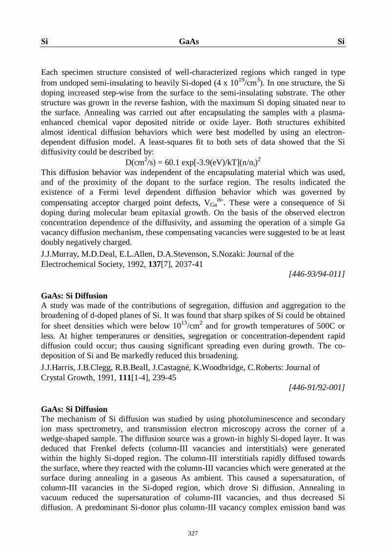
327
Si GaAs Si
Each specimen structure consisted of well-characterized regions which ranged in typefrom undoped semi-insulating to heavily Si-doped (4 x 10¹⁹/cm3). In one structure, the Sidoping increased step-wise from the surface to the semi-insulating substrate. The otherstructure was grown in the reverse fashion, with the maximum Si doping situated near tothe surface. Annealing was carried out after encapsulating the samples with a plasma-enhanced chemical vapor deposited nitride or oxide layer. Both structures exhibitedalmost identical diffusion behaviors which were best modelled by using an electron-dependent diffusion model. A least-squares fit to both sets of data showed that the Sidiffusivity could be described by:
D(cm2/s) = 60.1 exp[-3.9(eV)/kT](n/ni)2
This diffusion behavior was independent of the encapsulating material which was used,and of the proximity of the dopant to the surface region. The results indicated theexistence of a Fermi level dependent diffusion behavior which was governed bycompensating acceptor charged point defects, VGa
m-. These were a consequence of Sidoping during molecular beam epitaxial growth. On the basis of the observed electronconcentration dependence of the diffusivity, and assuming the operation of a simple Gavacancy diffusion mechanism, these compensating vacancies were suggested to be at leastdoubly negatively charged.J.J.Murray, M.D.Deal, E.L.Allen, D.A.Stevenson, S.Nozaki: Journal of theElectrochemical Society, 1992, 137[7], 2037-41
[446-93/94-011]
GaAs: Si DiffusionA study was made of the contributions of segregation, diffusion and aggregation to thebroadening of d-doped planes of Si. It was found that sharp spikes of Si could be obtainedfor sheet densities which were below 1013/cm2 and for growth temperatures of 500C orless. At higher temperatures or densities, segregation or concentration-dependent rapiddiffusion could occur; thus causing significant spreading even during growth. The co-deposition of Si and Be markedly reduced this broadening.J.J.Harris, J.B.Clegg, R.B.Beall, J.Castagné, K.Woodbridge, C.Roberts: Journal ofCrystal Growth, 1991, 111[1-4], 239-45
[446-91/92-001]
GaAs: Si DiffusionThe mechanism of Si diffusion was studied by using photoluminescence and secondaryion mass spectrometry, and transmission electron microscopy across the corner of awedge-shaped sample. The diffusion source was a grown-in highly Si-doped layer. It wasdeduced that Frenkel defects (column-III vacancies and interstitials) were generatedwithin the highly Si-doped region. The column-III interstitials rapidly diffused towardsthe surface, where they reacted with the column-III vacancies which were generated at thesurface during annealing in a gaseous As ambient. This caused a supersaturation, ofcolumn-III vacancies in the Si-doped region, which drove Si diffusion. Annealing invacuum reduced the supersaturation of column-III vacancies, and thus decreased Sidiffusion. A predominant Si-donor plus column-III vacancy complex emission band was

328
Si GaAs Si
found in spectra from the Si-diffused region. The results supported the concept of avacancy-assisted mechanism for Si diffusion and impurity-induced disordering.L.Pavesi, N.H.Ky, J.D.Ganière, F.K.Reinhart, N.Baba-Ali, I.Harrison, B.Tuck, M.Henini:Journal of Applied Physics, 1992, 71[5], 2225-37
[446-86/87-002]
Figure 6: Diffusivity of Si in GaAs
GaAs: Si DiffusionThe diffusion of Si was investigated by using sources from various tie-triangle regions inthe Si-Ga-As phase diagram. This ensured constant chemical potentials for the 3components under isothermal conditions. The Si profiles were determined by usingsecondary ion mass spectrometry, and were found to be very different for the varioustypes of source. The Ga-Si-GaAs tie-triangle source produced p-type Si doping with aconcentration-independent diffusion coefficient. A neutral As or Ga vacancy was thoughtto be the predominant mobile defect under these conditions. The use of As-rich sourcesfrom 2 tie-triangle regions, or a Si-GaAs tie-line source, produced Si donor diffusion witha concentration-dependent diffusion behavior. The concentration-dependent diffusion
1.0E-19
1.0E-18
1.0E-17
1.0E-16
1.0E-15
1.0E-14
1.0E-13
1.0E-12
1.0E-11
7 8 9 10 11 12 13 14
table 21table 22table 23table 24table 25
104/T(K)
D (c
m2 /s
)

329
Si GaAs Si
coefficients of donor Si for As-rich source diffusion were related to the net ionized donorconcentration, and exhibited 3 different regions. These were an intrinsic regime, anintermediate regime, and a saturation regime. It was proposed that Ga vacancies wereresponsible for donor diffusion; with a VGa
0 and/or VGa- mechanism for the intrinsic
regime and a VGa--related mechanism for the extrinsic and saturation regimes. The use of
a Si-GaAs tie-line source produced 2 branch-type profiles which were intermediatebetween the As-rich and Ga-rich diffusion cases.K.H.Lee, D.A.Stevenson, M.D.Deal: Journal of Applied Physics, 1990, 68[8], 4008-13
[446-86/87-011]
Table 21Diffusivity of Si in GaAs
Temperature (C) D (cm2/s)850 2.5 x 10⁻¹⁵
800 7.8 x 10⁻¹⁶
750 4.0 x 10⁻¹⁶
700 2.3 x 10⁻¹⁶
650 3.7 x 10⁻¹⁷
GaAs: Si DiffusionThe effect of impurities upon the creation of Ga vacancies in Si-doped material, grown ona Be-doped epilayer by molecular beam epitaxy, was investigated by means of slowpositron beam measurements. It was found that doping with Si enhanced the creation ofGa vacancies. The results supported a theoretical model in which the creation of Gavacancies was explained in terms of a change in the-Fermi level position due to Sidoping. It was also suggested that Si atoms diffused as a neutral complex, SiGa-VGa, ratherthan as SiGa-SiAs. A change in the S-parameter distribution at the interface between Si-doped and Be-doped regions was explained in terms of a so-called Be carry-forwardeffect which occurred during the growth of Si-doped GaAs on a Be-doped epilayer.J.L.Lee, L.Wei, S.Tanigawa, M.Kawabe: Journal of Applied Physics, 1990, 68[11], 5571-5
[446-86/87-012]
322 GaAs: Si DiffusionThis dopant diffused extensively after implantation and long-term annealing. The resultscould be explained by assuming that the diffusivity depended upon the square of theelectron concentration. The dopant diffusion was affected by the presence of implantationdamage; the higher the concentration of extended defects, the slower being the diffusivityas compared with the values for conventional diffusion from a solid source. If the samplewas amorphized during implantation, extended defects did not form and the diffusivity ofthe ion was very close to that in material which had been diffused from a solid source.When amorphization did not occur, extended defects formed after implantation, and

330
Si GaAs Si
diffusion was inhibited; especially after low doses, in the short term, or at lowtemperatures. The higher the density of extended defects, the greater was the suppressionof diffusion. The diffusion was time-dependent. It was concluded that the results (table22) were consistent with a diffusion mechanism in which the mobile species was thedonor that was coupled with a charged Ga vacancy. The equilibrium vacancyconcentration was thought to be suppressed by the presence of extended defects and/orexcess Ga interstitials which resulted from implantation.E.L.Allen, J.J.Murray, M.D.Deal, J.D.Plummer, K.S.Jones, W.S.Rubart: Journal of theElectrochemical Society, 1991, 138[11], 3440-9
[446-84/85-016]
Table 22Diffusivity of Implanted Si in GaAs
Dose (/cm2) Temperature (C) D (cm2/s)5 x 1015 950 2.5 x 10⁻¹⁵
1 x 10¹⁴ 900 2.6 x 10⁻¹⁵
1 x 10¹⁵ 900 2.0 x 10⁻¹⁵
1 x 10¹⁵ 900 1.2 x 10⁻¹⁵
1 x 10¹⁵ 900 8.3 x 10⁻¹⁶
1 x 10¹⁵ 900 6.2 x 10⁻¹⁶
1 x 10¹⁴ 900 4.4 x 10⁻¹⁶
1 x 10¹⁴ 900 3.0 x 10⁻¹⁶
1 x 10¹⁴ 900 2.2 x 10⁻¹⁶
1 x 10¹⁵ 900 1.3 x 10⁻¹⁶
5 x 10¹⁵ 850 1.4 x 10⁻¹⁶
1 x 10¹⁵ 850 4.2 x 10⁻¹⁷
5 x 10¹⁵ 750 7.5 x 10⁻¹⁸
5 x 10¹⁴ 750 3.7 x 10⁻¹⁸
5 x 10¹⁴ 750 1.8 x 10⁻¹⁸
1 x 10¹⁵ 750 1.0 x 10⁻¹⁸
1 x 10¹⁴ 850 1.3 x 10⁻¹⁷
1 x 10¹⁴ 900 1.4 x 10⁻¹⁷
1 x 10¹⁴ 900 2.9 x 10⁻¹⁷
1 x 10¹⁵ 900 4.0 x 10⁻¹⁷
1 x 10¹⁴ 900 5.4 x 10⁻¹⁷
1 x 10¹⁴ 950 5.0 x 10⁻¹⁶
GaAs: Si DiffusionThe behavior of Si, after being initially d-doped into very pure gas-source molecular beamepitaxial GaAs layers, was studied by using capacitance-voltage profiling. A non-linear

331
Si GaAs Si
behavior of the diffusivity of Si as a function of the reciprocal temperature was observed.This was explained in terms of a 2-component Arrhenius dependence in which theactivation energies changed by 1.5eV. When Si diffusion was governed by the loweractivation energy, the impurity profile grew in width as a linear function of the annealingtime. Deviations of the measured Si diffusivity from classical impurity diffusion behaviorwere attributed to the existence of a non-equilibrium concentration of vacancies whichwas generated at the d-source position during annealing.J.E.Cunningham, T.H.Chui, W.Jan, T.Y.Kuo: Applied Physics Letters, 1991, 59[12],1452-4
[446-84/85-016]
GaAs: Si DiffusionSamples which had been implanted with 220keV Si ions to doses ranging from 3 x 10¹³ to1015/cm2, and annealed at 850C, were studied. By using transmission electronmicroscopy, voids were observed in samples with implanted doses of more than 3 x10¹⁴/cm2; after annealing times which were as short as 5s. In the same region where voidswere found, capacitance-voltage measurements revealed abnormally low electronconcentrations. Also in the same region, secondary ion mass spectrometry measurementsdetected anomalies in the Si concentration profiles. It was therefore deduced that Siredistribution had occurred. At high Si doses, the onset of void formation, the abnormallylow electron concentration, and the Si accumulation anomaly were concurrent. On thebasis of the results, it was concluded that voids inhibited electrical activity and led to theSi diffusion anomaly.S.Chen, S.T.Lee, G.Braunstein, K.Y.Ko, L.R.Zheng, T.Y.Tan: Japanese Journal ofApplied Physics, 1990, 29[11], L1950-3
[446-81/82-010]
GaAs: Si DiffusionThe growth of Si-doped liquid-encapsulated Czochralski material exhibited a significantdeviation, in Si incorporation, from that which was predicted by a classical segregationmodel. It was usually expected that, for a given impurity segregation coefficient, dopantincorporation throughout the crystal could be calculated with fairly good accuracy.Profiles for Te-doped liquid-encapsulated Czochralski material gave a closeapproximation to this classical model. However, in the case of Si-doped material, thedopant distribution in the crystals deviated significantly from the segregation model. Insome cases, this deviation amounted to several orders of magnitude. The degree ofdeviation was found to depend upon the growth conditions. The present work wasperformed in order to understand the source of the deviation from the model and to permitaccurate account to be taken of Si incorporation. Therefore, Si-doped crystals were grownby using a low-pressure liquid-encapsulated Czochralski technique and were intended tobe doped with between 1016 and 1018/cm3. The actual dopant incorporation wassignificantly lower than that predicted by the segregation model, and the axial dopantvariation was much too flat. Also, in spite of the use of intentional Si doping, a significantnumber of the crystals was semi-insulating. An analysis of the experimental data showed

332
Si GaAs Si
that this doping behavior could not be explained by assuming the existence of anunknown compensating impurity. A different model was developed which was consistentwith all of the observations and which provided an accurate account of Si incorporation.An understanding of the Si incorporation anomaly permitted successful process changesand improvements to be made. This model explained the observed anomaly by takingaccount of Si diffusion between the GaAs melt and the B2O3 encapsulant, as well as ofpermanent Si trapping in the B2O3. When the interaction of Si with B2O3 was taken intoaccount, the Si incorporation obeyed the segregation model and the anomaly vanished.A.Flat: Journal of Crystal Growth, 1991, 109[1-4], 224-7
[446-81/82-011]
Table 23Diffusivity of Si in GaAs
Temperature (C) D (cm2/s)1000 1.5 x 10⁻¹²
950 4.1 x 10⁻¹³
900 3.1 x 10⁻¹⁴
800 5.7 x 10⁻¹⁵
705 1.0 x 10⁻¹⁶
GaAs: Si DiffusionThe lateral variation in the emission energy of GaAs which had been masklessly grownon V-grooved Si was studied by using cathodoluminescence wavelength imaging. Thisnew experimental approach permitted, for the first time, the direct visualization andquantification of the extreme homogeneity of this novel growth mode and of the lateralvariations of Si impurity incorporation into such semiconductor microstructures. It wasthus an important method for characterizing micro-patterned opto-electronic monolithicintegrated circuits.M.Grundmann, J.Christen, D.Bimberg, A.Hashimoto, T.Fukunaga, N.Watanabe: AppliedPhysics Letters, 1991, 58[19], 2090-2
[446-81/82-012]
323 GaAs: Si DiffusionCapacitance-voltage methods were used to profile d-doped GaAs layers which had beengrown on Si substrates via metalorganic chemical vapor deposition. It was found thatthere was a close correlation between dislocation densities, in the epitaxial layers, and theassociated diffusion coefficients. After rapid thermal annealing (800-1000C, 7s), thediffusion data (table 23) could be described by:
D(cm2/s) = 30 exp[-3.4(eV)/kT]

333
Si GaAs Si
for a relatively thick buffer layer of 0.0033mm. It was concluded that the dislocation-enhanced diffusion of Si impurities was appreciable, and that the inclusion of an0.003mm buffer layer was insufficient to prevent the diffusion of impurities.Y.Kim, M.S.Kim, S.K.Min, C.Lee: Journal of Applied Physics, 1991, 69[3], 1355-8
[446-78/79-014]
GaAs: Si DiffusionHigh depth-resolution secondary ion mass spectrometry profiling was used to investigatethe broadening of d-doped planes of Si plus Be in material which had been prepared byusing molecular beam epitaxial methods. It was confirmed that concentration-dependentdiffusion was the predominant broadening process for Be at growth temperatures of lessthan 600C. By incorporating Si atoms into the same plane, it was shown that thebroadening could be completely inhibited. This suggested that the rapid diffusion processresulted from mutual repulsion between the BeGa
- ions, and was prevented by the reversefield which arose from SiGa
+ ions or by the formation of low-mobility SiGa+-BeGa
-
complexes. The rapid diffusion of Si as SiGa-SiAs pairs was also reduced. The latter wasattributed to a Fermi-level effect, with compensation by Be tending to reduce theprobability of SiAs formation. The surface segregation of Si was unaffected, whereas thatof Be was reduced. This indicated that the surface fields which existed during growthcontributed to the behavior of Be, but not to that of Si.J.J.Harris, J.B.Clegg, R.B.Beall, J.Castagné: Semiconductor Science and Technology,1990, 5[7], 785-8
[446-76/77-007]
GaAs: Si DiffusionA quantitative model was proposed for the behavior of Si. The model took account of thefact that Si was an amphoteric impurity which acted as a shallow donor when it occupiedthe Ga site (SiGa
+) and as a shallow acceptor when it occupied the As site (SiAs-). Both
SiGa+ and SiAs
- existed at high concentrations. The amphoteric behavior of Si could beviewed as being an effect of the Fermi level. It was assumed that SiGa
+ and SiAs- diffused
on the Ga and As sub-lattices, respectively. Thus, the diffusion of SiGa+ and SiAs
- wasgoverned by the variously charged Ga vacancies and As vacancies (or self-interstitials)respectively. The experimentally observed Si diffusivity was concentration dependent,and this was attributed to the amphoteric nature of Si as well as to another effect of theFermi level. The latter involved its influence upon the concentrations of charged point-defect species. Satisfactory quantitative descriptions of available experimental data wereobtained. An analysis of results on the diffusion of Si into a Sn-doped GaAs substratesuggested that a previously proposed Si-pair diffusion model was unfavorable.S.Yu, U.M.Gösele, T.Y.Tan: Journal of Applied Physics, 1989, 66[7], 2952-61
[446-74-012]
334
Si GaAs Si
GaAs: Si DiffusionA model for Si diffusion was developed which was based upon the formation of SiGa
+-VGa
- pairs. By using recent data on the diffusivity of Ga vacancies, it was shown that thepair diffusion coefficient was approximately equal to 75% of the former value. Thepredictions of the model were found to be in good agreement with Si diffusion data.K.B.Kahen: Journal of Applied Physics, 1989, 66[12], 6176-8
[446-74-012]
GaAs: Si DiffusionThe diffusion of Si was studied after implanting Si into un-doped, Se-, Si- or Zn-dopedmaterial. The diffusion of grown-in Si in epitaxial layer structures was also studied. Nodiffusion was detected in un-doped or Zn-doped material, while a moderate amount ofdiffusion was detected in Si-doped samples. A significant amount of diffusion occurred inSe-doped material and in non-implanted Si-doped epitaxial samples. The results indicatedthat diffusion was controlled by a Fermi-level mechanism which probably involvedionized Ga vacancies, and that implantation damage inhibited diffusion by keeping theelectron concentration and/or the ionized Ga vacancy concentration at a low level.J.J.Murray, M.D.Deal, D.A.Stevenson: Applied Physics Letters, 1990, 56[5], 472-4
[446-74-012]
GaAs: Si DiffusionThe effect of the substrate temperature, during molecular beam epitaxial growth, upon themigration of Si atoms in d-doped or planar-doped GaAs was investigated by usingsecondary ion mass spectrometry. The results for d-doped GaAs revealed a measurablespread of Si, which increased by about 8nm when the substrate temperature was increasedfrom 580 to 640C. For substrate temperatures below 580C, the measured width of the Siprofile was limited by the resolution of the secondary ion mass spectrometer.Magnetotransport measurements were also performed in order to determine dopantspreading. The Si migration which was measured by means of secondary ion massspectrometry was in qualitative agreement with the transport results. However, thesecondary ion mass spectrometry data indicated larger Si areal densities. Twomechanisms, auto-compensation and electron localization by a DX center, were believedto be responsible for the latter observations.A.M.Lanzillotto, M.Santos, M.Shayegan: Applied Physics Letters, 1989, 55[14], 1445-7
[446-72/73-002]
GaAs: Si DiffusionElectron-beam deposited films of phosphosilicate were used for the encapsulation of Si-implanted material during post-implantation annealing. Depth profiles which were inexcellent agreement with the Lindhard-Scharff-Schiott curves were obtained by using100nm thick films and by annealing for 0.5h at 850C. The diffusion coefficient of

335
Si GaAs Si
implanted Si was found to be an order of magnitude smaller for phosphosilicate filmsthan for conventional plasma-assisted chemical vapor deposited SiO2 films.S.Singh, F.Baiocchi, A.D.Butherus, W.H.Grodkiewicz, B.Schwartz, L.G.Van Uitert,L.Yesis, G.J.Zydzik: Journal of Applied Physics, 1988, 64[8], 4194-8
[446-72/73-011]
GaAs: Si DiffusionLayers were grown, by molecular beam epitaxy, at a substrate temperature of 520C. Thelayers contained three d-doped planes, with Si concentrations of 4 x 10¹², 1013 or 4 x10¹³/cm3, and were annealed at temperatures of up to 648C. Secondary ion massspectroscopy and capacitance-voltage methods were then used to monitor broadening ofthe profiles. It was found that the most lightly doped plane gave a near-Gaussian profile,and the diffusion coefficient was comparable with published data on the simple diffusionof isolated SiGa atoms. The more highly doped planes exhibited complex profiles with 2components; in which some of the atoms were confined to the original plane, while therewas an essentially square-shaped profile of fast-diffusing atoms. A comparison of the 2types of experimental data suggested that the formation of Si islands took place duringdeposition of the d-doped plane. This gave rise to electrically inactive atoms which couldthen diffuse into the surrounding material during heat treatment.R.B.Beall, J.B.Clegg, J.Castagné, J.J.Harris, R.Murray, R.C.Newman: SemiconductorScience and Technology, 1989, 4[12], 1171-5
[446-72/73-011]
GaAs: Si DiffusionQuantum oscillations in the magnetoresistance of Si-doped material were analyzed inorder to obtain the electron densities of the electrical sub-bands. These densities werecompared with the results for self-consistently calculated sub-band structures of d-dopedmaterial in which the spread of Si dopant atoms in the growth direction was a fittingparameter. The results indicated that there was a negligible spread in structures whichwere grown at substrate temperatures of up to 530C. In structures which were grown athigher substrate temperatures, there was a measurable spread. This increased withincreasing substrate temperature. At a substrate temperature of 640C, the Si spread wasabout 22nm. An examination of the three-dimensional Si densities in these layersindicated that the predominant mechanism of Si spreading at substrate temperaturesgreater than 600C was the Si migration which was necessary in order to satisfy the solidsolubility limit.M.Santos, T.Sajoto, A.Zrenner, M.Shayegan: Applied Physics Letters, 1988, 53[25],2504-6
[446-64/65-163]
GaAs: Si DiffusionA review was presented of self-diffusion mechanisms and doping-enhanced superlatticedisordering. The mechanism of enhanced superlattice disordering due to Si doping was aFermi-level effect which increased the concentrations of charged point defects. The
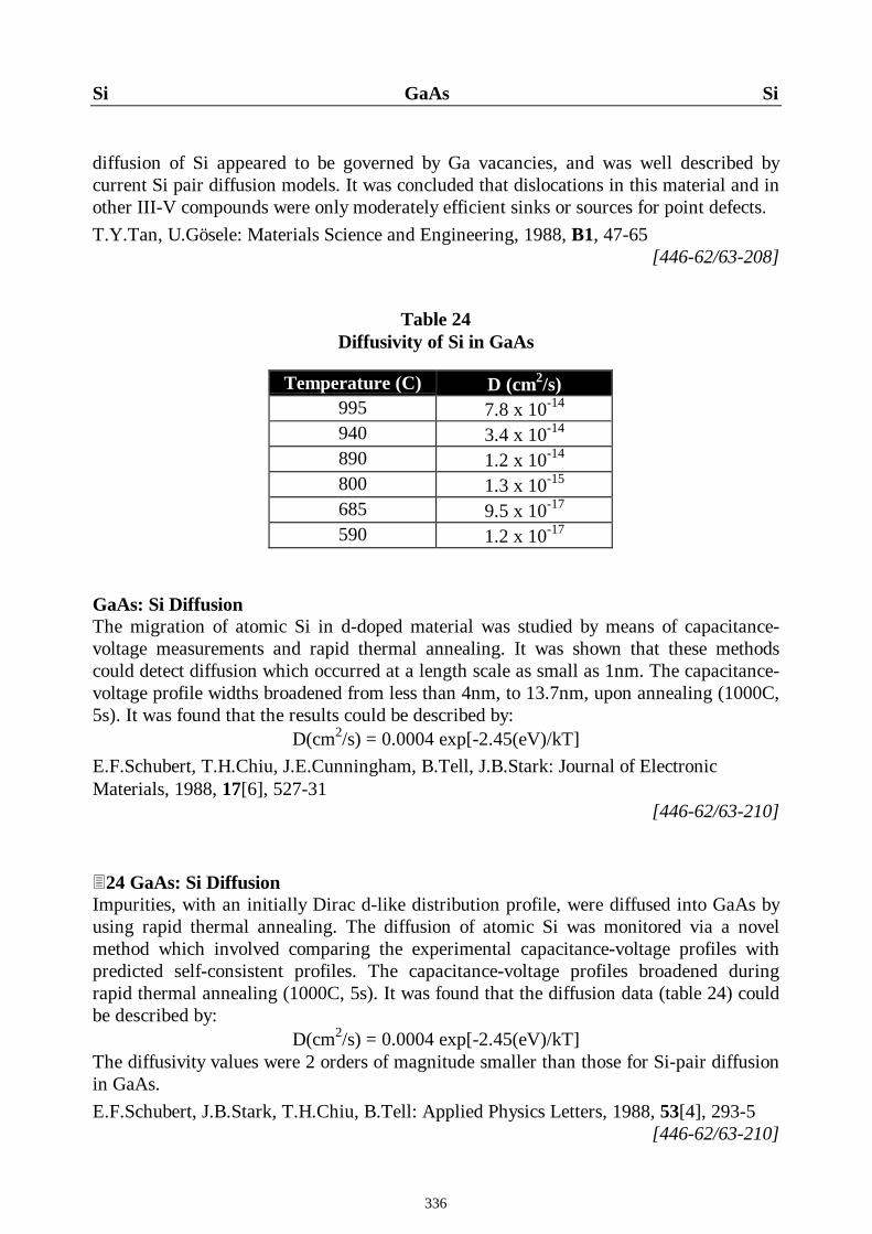
336
Si GaAs Si
diffusion of Si appeared to be governed by Ga vacancies, and was well described bycurrent Si pair diffusion models. It was concluded that dislocations in this material and inother III-V compounds were only moderately efficient sinks or sources for point defects.T.Y.Tan, U.Gösele: Materials Science and Engineering, 1988, B1, 47-65
[446-62/63-208]
Table 24Diffusivity of Si in GaAs
Temperature (C) D (cm2/s)995 7.8 x 10⁻¹⁴
940 3.4 x 10⁻¹⁴
890 1.2 x 10⁻¹⁴
800 1.3 x 10⁻¹⁵
685 9.5 x 10⁻¹⁷
590 1.2 x 10⁻¹⁷
GaAs: Si DiffusionThe migration of atomic Si in d-doped material was studied by means of capacitance-voltage measurements and rapid thermal annealing. It was shown that these methodscould detect diffusion which occurred at a length scale as small as 1nm. The capacitance-voltage profile widths broadened from less than 4nm, to 13.7nm, upon annealing (1000C,5s). It was found that the results could be described by:
D(cm2/s) = 0.0004 exp[-2.45(eV)/kT]E.F.Schubert, T.H.Chiu, J.E.Cunningham, B.Tell, J.B.Stark: Journal of ElectronicMaterials, 1988, 17[6], 527-31
[446-62/63-210]
324 GaAs: Si DiffusionImpurities, with an initially Dirac d-like distribution profile, were diffused into GaAs byusing rapid thermal annealing. The diffusion of atomic Si was monitored via a novelmethod which involved comparing the experimental capacitance-voltage profiles withpredicted self-consistent profiles. The capacitance-voltage profiles broadened duringrapid thermal annealing (1000C, 5s). It was found that the diffusion data (table 24) couldbe described by:
D(cm2/s) = 0.0004 exp[-2.45(eV)/kT]The diffusivity values were 2 orders of magnitude smaller than those for Si-pair diffusionin GaAs.E.F.Schubert, J.B.Stark, T.H.Chiu, B.Tell: Applied Physics Letters, 1988, 53[4], 293-5
[446-62/63-210]

337
Si GaAs Si
Table 25Diffusivity of Si in GaAs
Temperature (C) D (cm2/s)960 7.5 x 10⁻¹⁵
955 4.7 x 10⁻¹⁵
895 4.4 x 10⁻¹⁵
900 2.0 x 10⁻¹⁵
795 2.0 x 10⁻¹⁵
790 1.1 x 10⁻¹⁵
695 1.0 x 10⁻¹⁵
695 5.1 x 10⁻¹⁶
645 1.9 x 10⁻¹⁶
590 7.8 x 10⁻¹⁷
535 4.9 x 10⁻¹⁷
605 3.7 x 10⁻¹⁷
485 2.0 x 10⁻¹⁷
590 1.9 x 10⁻¹⁷
555 8.2 x 10⁻¹⁸
515 1.0 x 10⁻¹⁸
GaAs: Si DiffusionHigh-quality samples were prepared by means of chemical beam epitaxy, at a substratetemperature of 500C, by using triethylgallium and arsine. Capacitance-voltagemeasurements of Si-doped material revealed profile widths of 2.2nm at 300K and 1.8nmat 77K. This indicated that a high degree of Si spatial localization had been achieved.Subsequent annealing treatments showed that appreciable Si segregation and diffusionoccurred at a growth temperature of about 600C. The capacitance-voltage widths ofannealed doped structures provided a good estimate of the diffusion coefficient of Si inGaAs.T.H.Chiu, J.E.Cunningham, B.Tell, E.F.Schubert: Journal of Applied Physics, 1988,64[3], 1578-80
[446-61-067]
325 GaAs: Si DiffusionPlanar confinement, diffusion, and surface segregation results were reported for Si whichhad been d-doped into GaAs. In the case of gas-source molecular beam epitaxy, the Sidiffusion (table 25) as a function of the reciprocal annealing temperature exhibited an

338
Si GaAs Si
unique 2-component Arrhenius form in which the activation energies differed by thefundamental GaAs band-gap energy of 1.5eV.J.E.Cunningham, T.H.Chiu, B.Tell, W.Jan: Journal of Vacuum Science and TechnologyB, 1990, 8[2], 157-9
[446-74-012]
GaAs: Si DiffusionSecondary ion mass spectroscopy and carrier concentration measurements were used tocharacterize Si diffusion into GaAs wafers which contained 2 fundamentally differenttypes of donor. These were column-IV donors (Si, Sn) and column-VI donors (Se, Te). Adecrease in the Si diffusion rate was found in material which contained column-VI donorsas compared with that which contained column-IV donors. This trend was consistent witha model in which Si diffused as donor Ga-vacancy complexes. The decrease in the Sidiffusion coefficient was attributed to the greater binding energy of column-VI donor Ga-vacancy nearest-neighbor complexes. This reduced the numbers of free Ga vacancieswhich were available to complex with the Si.D.G.Deppe, N.Holonyak, J.E.Baker: Applied Physics Letters, 1988, 52[2], 129-31
[446-60-003]
GaAs: Si DiffusionData were presented which demonstrated that the surface encapsulant and As4 over-pressure strongly affected Si. An increase in the As4 over-pressure resulted in an increasein the diffusion depth. No band-edge exciton was observed during absorption on materialthat was diffused with Si, in spite of the high degree of compensation.L.J.Guido, W.E.Plano, D.W.Nam, N.Holonyak, J.E.Baker, R.D.Burnham, P.Gavrilovic:Journal of Electronic Materials, 1988, 17[1], 53-6
[446-60-004]
GaAs: Si DiffusionThe diffusion profiles of buried Si dopant which had been implanted by using a focussedion beam were determined after annealing. The diffusion coefficient of the Si wasdetermined by fitting the results of computer calculations. Concentration-dependentdiffusion of Si which had been introduced by using a molecular beam was observed.However, the diffusion coefficient of Si which had been introduced by using a focussedion beam was undetectably small when compared with that of Be at 850C.T.Morita, J.Kobayashi, T.Takamori, A.Takamori, E.Miyauchi, H.Hashimoto: JapaneseJournal of Applied Physics, 1987, 26[8], 1324-7
[446-55/56-005]
GaAs: Si DiffusionJunction-depth measurements, performed using scanning electron microscopy andsecondary ion mass spectroscopy, were used to characterize Si diffusion in GaAs crystalswhich contained various amounts of Zn background doping. The Zn concentration was

339
Si GaAs Si
found to control Si diffusion. This behavior was attributed to a shift in the Fermi levelwith increasing n-type doping. Also, the electric field which was due to the p-n junctionthat formed at the Si diffusion front had a large effect upon the Zn background dopingprofile.D.G.Deppe, N.Holonyak, F.A.Kish, J.E.Baker: Applied Physics Letters, 1987, 50[15],998-1000
[446-51/52-116]
GaAs: Si DiffusionA new method for self-aligned Si-Zn diffusion was described. In this method, closed-tubeSi diffusion was carried out by using a sputtered SiNx film. Then, Zn diffusion which wasself-aligned to the Si diffusion window was carried out by re-using the SiNx film as amask. The key factor was that the SiNx film should have the correct refractive indexprofile.W.X.Zou, R.Boudreau, H.T.Han, T.Bowen, S.S.Shi, D.S.L.Mui, J.L.Merz: Journal ofApplied Physics, 1995, 77[12], 6244-6
[446-121/122-045]
GaAs: Si DiffusionThe reported anomalous so-called up-hill diffusion behavior of implanted Si in thismaterial was simulated. The up-hill diffusion had been found to be implantation-dosedependent. No up-hill diffusion was observed below a threshold dose of 3 x 10¹⁴/cm2. Itwas suggested here that the anomalous behavior was due to the formation of vacancyclusters when the implantation dose was sufficiently high. Atoms of Si were assumed tomigrate through the Ga vacancies, which were comparatively mobile. On the other hand,the immobile clusters collected Si atoms around the vacancy peak; thus resulting in up-hill diffusion. A dip in the carrier concentration profile also occurred at high implantationdoses. The occurrence of this dip was attributed to the effect of the trapping of Si atomsinto clusters where the former were not electrically activated.V.C.Lo, J.Z.Sun: Modelling and Simulation in Materials Science and Engineering, 1996,4[6], 613-21
[446-157/159-339]
GaAs: Si DiffusionThe diffusion of Si was carried out (900C, 5h, As pressure), from a 50nm sputtered filmand into undoped semi-insulating material or Te-doped or Zn-doped liquid-encapsulatedCzochralski material. Secondary ion mass spectroscopy and spreading resistancetechniques were used to characterize the Si in-diffusion profiles. Lattice defects in highlySi-doped diffusion regions were studied as a function of the post-diffusion heat treatment(700C, 0.25h; 1000C, 0.5h) via the transmission electron microscopy of plan-view andcross-sectional samples. Two types of defect were observed in the diffused region. Thesewere perfect prismatic loops of interstitial type on 110 planes, and Frank faulted loopson 111; again of interstitial type. Defect formation, and the role of Si in defectgeneration, were explained in terms of a negative temperature dependence of the thermal

340
Si GaAs Si
equilibrium concentrations of VGa3-; which were assumed to mediate Si diffusion under
highly n-doped conditions. Cathodoluminescence spectra at 4 and 77K were obtainedfrom the diffusion layer. It was found that the Si diffusion affected the band-gapluminescence and generated 2 deep-level emission bands in the 0.9 to 1.3eV spectralregion. It was suggested that these deep levels were associated with diffusion-induceddefects and defect complexes.L.Herzog, U.Egger, O.Breitenstein, H.G.Hettwer: Materials Science and Engineering B,1995, 30[1], 43-53
[446-134/135-125]
GaAs: Si DiffusionThe migration of Si acceptors (Si on As sites) in δ-doped GaAs which had been grownonto GaAs(111)A, was investigated by means of secondary ion mass spectrometry. It wasfound that the diffusion parameters for GaAs(111)A differed from those for GaAs(001).The diffusion coefficient in GaAs(111)A was smaller than that in GaAs(001), and theactivation energy in GaAs(111)A was higher than that in GaAs(001). The diffusionmechanism of Si in GaAs(111)A was investigated by means of photoluminescence and itwas found that, in p-type layers, Si-donors (Si on Ga sites) diffused easily to As sites. Thedata on Si acceptor diffusion could be described by:
D(cm2/s) = 0.0114 exp[-2.74(eV)/kT]The results indicated that Si-acceptors were more stable than Si donors.M.Hirai, H.Ohnishi, K.Fujita, P.Vaccaro, T.Watanabe: Journal of Crystal Growth, 1995,150[1-4], 209-13
[446-127/128-120]
GaAs: Si DiffusionAn investigation was made of the fast diffusion of Si from deposited surface layers whenoxidized in an Ar/H2O ambient. This revealed the presence of excess As which wasformed by the oxidation of Ga which originated from the substrate, and was used toexplain the enhanced diffusion of Si into the substrate. The formation of SiO2 on thesurface during oxidation prevented the loss of the excess As, which then accumulated inthe remaining Si film. The use of higher H2O partial pressures during oxidation producedhigher As/Si ratios; thus resulting in an increase in Si diffusion depth and concentration.However, the n-type carrier concentration decreased with increasing As/Si ratios in theremaining Si layer. A second non-oxidizing annealing treatment, of samples from whichthe SiO2 and Si layer had been removed, had differing effects upon the carrierconcentration; depending upon whether the As was free to escape from the substrate. Theresults indicated that excess As-related defects, such as Ga vacancies, were probablyresponsible for n-type compensation in fast diffused samples.R.C.Keller, C.R.Helms: Applied Physics Letters, 1995, 67[3], 398-400
[446-123/124-162]
341
Si GaAs Si
GaAs: Si DiffusionThe diffusion of Si was studied by using secondary ion mass spectroscopic andtransmission electron microscopic methods after implanting it using energies rangingfrom 20 to 200keV and doses ranging from 1013 to 1014/cm2, followed by furnaceannealing. It was found that little or no diffusion occurred after implantation at energiesgreater than 100keV. At energies of less than 100keV, there was usually appreciabledopant redistribution; regardless of the peak implant concentration. Both concentration-dependent and concentration-independent diffusion was observed. The dislocation loopdensity varied inversely with the amount of diffusion as a function of implantationenergy. A standard Monte Carlo computer program was able to predict the trends in theimplant energy dependence of diffusion by considering the excess point defect contentwhich was produced by implantation. The effect of this excess defect dose and of surfaceeffects upon Si diffusion was consistent with vacancy-assisted diffusion.C.C.Lee, M.D.Deal, K.S.Jones, H.G.Robinson, J.C.Bravman: Journal of theElectrochemical Society, 1994, 141[8], 2245-9
[446-119/120-192]
GaAs: Si DiffusionImplantation of Si into (x11)A-oriented semi-insulating GaAs substrates (where x tookvalues of up to 4) was carried out. For comparison, (110)- and (100)-oriented substrateswere also implanted. No in-diffusion of Si was observed after annealing substrates withany orientation. A similar behavior was observed for Si implants in GaAs and for Si/B co-implants.M.V.Rao, H.B.Dietrich, P.B.Klein, A.Fathimulla, D.S.Simons, P.H.Chi: Journal ofApplied Physics, 1994, 75[12], 7774-8
[446-117/118-166]
GaAs: Si DiffusionDopant diffusion and defect formation were studied as a function of implantationtemperature in Si-implanted material. It was found that the diffusion of Si during post-implantation annealing decreased by a factor of 2.5 as the implantation temperature wasincreased from -2 to 40C. Within the same temperature range, the maximum depth anddensity of extrinsic dislocation loops increased by factors of 3 and 4, respectively.Rutherford back-scattering channelling measurements indicated that Si-implanted GaAsunderwent an amorphous to crystalline transition at Si implantation temperatures ofbetween -51 and 40C. A unified explanation was proposed, for the effects of implantationtemperature upon diffusion and dislocation formation, which was based upon knowndifferences in sputter yield between crystalline and amorphous semiconductors. Themodel assumed that the sputter yield was enhanced by amorphization at lowertemperatures; which increased the excess vacancy concentration. Estimates of the latter

342
Si GaAs Si
were obtained by simulating the diffusion profiles, and were found to be quantitativelyconsistent with sputter yield enhancement.H.G.Robinson, T.E.Haynes, E.L.Allen, C.C.Lee, M.D.Deal, K.S.Jones: Journal ofApplied Physics, 1994, 76[8], 4571-5
[446-117/118-166]
GaAs: Si DiffusionA study was made of the diffusion of Si in δ-doped layers of (111)A- or (100)-type, andof the evaporation of As atoms from the surfaces. It was found that the diffusion ofdopants in (111)A layers was slower than in (100), regardless of the presence of Asvacancies. On the other hand, diffusion in (100) layers was enhanced by the presence ofAs vacancies. It was noted that As atoms on the (111)A surface did not evaporate easily,as compared with those on the (100) surface.A.Shinoda, T.Yamamoto, M.Inai, T.Takebe, T.Watanabe: Japanese Journal of AppliedPhysics, 1993, 32[2-10A], L1374-6
[446-115/116-116]
GaAs: Si DiffusionFirst-principles calculations were presented for the vacancy-mediated diffusion of Si. Itwas shown that a DX-like mechanism facilitated the migration of lattice-site atoms intothe interstitial region, and that the dangling bonds of a second-nearest neighbor vacancyassisted migration through the interstitial region. Due to these 2 mechanisms, vacancy-assisted diffusion of Si occurred with a low-energy barrier.J.Dabrowski, J.E.Northrup: Physical Review B, 1994, 49[20], 14286-9
[446-115/116-117]
GaAs: Si DiffusionA study was made of molecular beam epitaxially grown samples which were δ-dopedwith Si and Al layers. Long-term diffusion annealing was carried out at temperaturesranging from 550 to 800C, and the concentration profiles were determined by means ofsecondary ion mass spectrometry. It was found that the results could be described by theexpression,
D(cm2/s) = 7.9 exp[-2.25(eV)/kT]The Si diffusion coefficients which were obtained were in good agreement with datawhich had been obtained by using rapid thermal annealing, capacitance-voltage profiling,and sandwiched diffusion sources. They differed from earlier measurements which hadbeen based upon the diffusion of implanted dopants that were much more widely spread.It was concluded that the more accurate data which resulted from δ-doping showed thatthe diffusion coefficient was an intrinsic parameter, provided that the amount of dopantand the dislocation density were kept sufficiently small.F.Bénière, R.Chaplain, M.Gauneau, V.Reddy, A.Régrény: Journal de Physique III, 1993,3[12], 2165-71
[446-115/116-119]

343
Si GaAs Si
GaAs: Si DiffusionVarious mechanisms of Si diffusion in GaAs were investigated by using first-principlesmolecular dynamics methods. It was found that the predominant mechanism involved themotion of negatively charged SiIII-VIII pairs via second-nearest neighbor jumps. Thismechanism explained the ability of Si to disorder superlattices (regardless of whether itwas introduced during growth or was in-diffused later), and the suppression ofinterdiffusion by compensation doping. The calculated activation energies were in verygood agreement with experimental data.B.Chen, Q.M.Zhang, J.Bernholc: Physical Review B, 1994, 49[4], 2985-8
[446-115/116-119]
GaAs: Si DiffusionIt was recalled that implantation damage was believed to play a significant role in dopantdiffusion. An attempt was made here to modify the point defect damage profile of 40keV29Si implants by chemically etching away the top 10nm of the sample after implantation.No Si diffusion was observed in these samples after annealing, whereas significant Siredistribution occurred in a similar sample which had received no post-implantationetching. The results of TRIM simulations predicted an excess Ga vacancy surface layer,and the presence of excess Ga interstitials deeper within the sample. It was thought that,by removing the vacancy-rich surface layer, the etch altered the implant damage profileand thus the diffusion behavior of Si. The surface effects of etching which were related toSi diffusion were shown to be consistent with a vacancy-assisted diffusion mechanism.There was some evidence that this model might be applicable to B implants in Si.C.C.Lee, M.D.Deal, J.C.Bravman: Applied Physics Letters, 1994, 64[24], 3302-4
[446-115/116-119]
GaAs: Si DiffusionA study was made of the transport properties of the 2-dimensional electron gas inannealed Si δ-doped structures. The diffusion rate of Si atoms was deduced from thetemperature dependence of the sub-band population. In samples with large self-compensation, it was found that the electron density increased after annealing attemperatures below 800C. After annealing at temperatures above 800C, there was areduction in the electron concentration of the 2-dimensional electron gas. The resultsshowed that, after annealing, the quantum mobility in the lowest sub-band increasedslightly, while the quantum mobility in the higher sub-bands markedly decreased.P.M.Koenraad, I.Bársony, A.F.W.Van der Stadt, J.A.A.J.Perenboom, J.H.Wolter:Materials Science Forum, 1994, 143-147, 663-8
[446-113/114-012]
GaAs: Si DiffusionThe diffusion of Si out of δ-planes in GaAs was investigated by means of high-resolutionX-ray diffractometry, infra-red absorption localized vibrational mode spectroscopy andsecondary ion mass spectroscopy. In the case of a Si δ-doped sample which had been
344
Si GaAs Si
grown at 400C with a Si areal concentration of 3.4 x 10¹⁴/cm2, the Si was confined to alayer which was no more than 0.5nm in thickness. After post-growth annealing (600C,3h), 22.6% of the Si remained on the δ-planes, while the remainder had diffusedhomogeneously throughout the epilayer to give a Si concentration of 2.1 x 10¹⁹/cm3.Localized vibrational mode spectroscopy indicated that these Si atoms were locatedmainly on Ga sites (SiGa). The Si atoms were also found to occupy As sites, or werepresent as SiGa-SiAs pairs, Si-X and SiGa-VGa complexes. At 950C, all of the Si haddiffused away from the δ-planes to form precipitates and dislocation loops near to thesurface.L.Hart, P.F.Fewster, M.J.Ashwin, M.R.Fahy, R.C.Newman: Materials Science Forum,1994, 143-147, 647-52
[446-113/114-013]
GaAs: Si DiffusionIt was recalled that, in n-type material, the diffusion of atoms which resided on the Gasub-lattice occurred mainly via Ga vacancies. In order to elucidate the microscopic detailsand energetics of these processes, local density approximation estimates were made of thetotal energies, electronic structures, and relaxed positions of atoms in microscopicconfigurations which were relevant to the diffusion of Si donors. It was found that a DX-like mechanism facilitated the migration of lattice site atoms into the interstitial region. Abond-passing mechanism was also identified, in which a second-nearest neighbor vacancyassisted migration through the interstitial region. Due to these 2 mechanisms, vacancy-assisted Si diffusion in n-type material was characterized by an energy barrier of about1.0eV.J.Dabrowski, J.Northrup: Materials Science Forum, 1994, 143-147, 1263-8
[446-113/114-013]
GaAs: Si DiffusionThe thermal equilibrium concentrations of the various negatively charged Ga vacancyspecies were calculated. The triply negatively charged Ga vacancy, VGa
3-, was studied inparticular because it dominated Ga self-diffusion and Ga/Al interdiffusion under intrinsicand n-doping conditions, as well as the diffusion of Si donor atoms which occupied Gasites.T.Y.Tan, H.M.You, U.M.Gösele: Applied Physics A, 1993, 56[3], 249-58
[446-111/112-050]
GaAs: Si DiffusionSamples were doped with Si to a concentration of about 2.7 x 10¹⁸/cm3 and were annealed(800 to 1000C, 3 to 20h) under As-rich or As-poor conditions. The Si out-diffusion wasmeasured by using the capacitance-voltage method and an electrochemical profiler. It wasfound that the Si diffusivity exhibited a marked dependence upon the As4 vapor phasepressure and upon the electron concentration. When reduced to intrinsic conditions,activation enthalpies of 3.91 and 4.19eV were obtained for As-rich and As-poor annealing
345
Si GaAs Si
conditions, respectively. On the basis of these results, it was concluded that Si out-diffusion was governed by the triply negatively charged vacancies, VGa
3-.H.M.You, U.M.Gösele, T.Y.Tan: Materials Science Forum, 1993, 117-118, 399-404
[446-111/112-051]
GaAs: Si DiffusionSamples of n-type and p-type d-doped material, grown by molecular beam epitaxy andwith quite high doses of Si, were investigated by means of transmission electronmicroscopy. The magnitude of the doses ranged from half a monolayer to 2 monolayers.The microscopic structures of the d-doped regions and of the adjacent epilayers wereobserved directly. The effect of impurity spreading upon the hetero-interfaces andsuperlattices was studied, and it was found that the Si atoms in Si d-doped samples wereconfined to within a few atomic layers. Stacking faults were found in d-doped sampleswhen they were grown at low temperatures. Their presence was attributed to local strainsthat were caused by heavy doping.D.G.Liu, J.C.Fan, C.P.Lee, K.H.Chang, D.C.Liou: Journal of Applied Physics, 1993,73[2], 608-14
[446-106/107-034]
GaAs: Si DiffusionThe lateral diffusion of sources during the selective growth of metalorganic vapor-phaseepitaxial Si-doped layers was analyzed. The diffusion lengths of Si species were deducedfrom the carrier concentration profiles which were measured by using Ramanspectroscopy and thickness profiling. On the basis of these diffusion lengths, it wasspeculated that the effective diffusion material was silyl arsine. It was suggested that therewas no difference between arsine and tertiary butyl arsine, as diffusion sources.N.Hara, K.Shiina, T.Ohori, K.Kasai, J.Komeno: Journal of Applied Physics, 1993, 74[2],1327-30
[446-106/107-036]
GaAs: Si DiffusionThe formation energy of Si donors, acceptors, and defect complexes were calculated. Theequilibrium concentrations of native defects and Si-defect complexes were deduced fromthese energies, as was the total solubility of Si. The calculated equilibrium solubility limitfor Si was in good agreement with experimental data. The (SiGa-VGa)2- complex occurredat relatively high concentrations under As-rich conditions, and could therefore mediate Siand Ga diffusion. It was concluded that the donor-vacancy complex was an importantcompensation mechanism in heavily doped GaAs.J.E.Northrup, S.B.Zhang: Physical Review B, 1993, 47[11], 6791-4
[446-106/107-036]
346
Si GaAs Si
GaAs: Si DiffusionAn experimental study was made of Si out-diffusion from GaAs, by using pre-dopedsamples. The results showed that the Si diffusivity depended upon the As4 vapor-phasepressure in the ambient, and upon the electron concentration in the crystal. It wasconcluded that, in GaAs, diffusion of the Si donor species which occupied Ga sites, SiGa
+,was governed by the triply negatively charged Ga vacancies, VGa
3-. However, the presentVGa
3--dominated SiGa+ out-diffusivities were larger, by many orders of magnitude, than
those which were obtained under Si in-diffusion conditions. A tentative explanation ofthis large difference was given in terms of an undersaturation of VGa
3- in intrinsic materialduring in-diffusion experiments, and of a supersaturation of VGa
3- which developedduring the out-diffusion of Si from n-type Si-doped material.H.M.You, U.M.Gösele, T.Y.Tan: Journal of Applied Physics, 1993, 73[11], 7207-16
[446-106/107-037]
GaAs: Si DiffusionHeavily Si-doped (5 x 10¹⁹/cm3) low-temperature GaAs, sandwiched between undopedlow-temperature GaAs layers, was grown by using molecular beam epitaxy and wasannealed at up to 900C. Transmission electron microscopy showed that, within the firstfew minutes of annealing, an accumulation of As precipitates formed near to eachdoped/undoped low-temperature interface. During further annealing, Si segregation to Asprecipitates was detected, using secondary ion mass spectroscopy, in the form of delta-like peaks at the As precipitate accumulations. It was found that the Si diffusioncoefficient was initially independent of concentration, at a value of 2.5 x 10⁻¹³cm2/s, andwas comparable to diffusion under intrinsic conditions in As-rich material when grown atnormal temperatures. During annealing for 1h, the Si concentration in the As precipitatesreached 2.5 x 10²⁰/cm3.K.L.Kavanagh, J.C.P.Chang, P.D.Kirchner, A.C.Warren, J.M.Woodall: Applied PhysicsLetters, 1993, 62[3], 286-8
[446-106/107-038]
GaAs: Si DiffusionThe diffusion of Si from a novel diffusion source, consisting of an undoped SiOx/SiNdouble-layered film, was studied by rapid thermal annealing at 860 to 940C. Thecharacteristics of the Si-diffused layers were investigated by using secondary ion massspectrometric, capacitance-voltage, and Hall methods. The carrier profiles exceeded 2 x10¹⁸/cm3, and featured an abrupt diffusion front. A maximum electron concentration of 6x 10¹⁸/cm3 was obtained at 940C. The diffused Si profiles were consistent with theoperation of SiGa
+-VGa- pair diffusion.
S.Matsushita, S.Terada, E.Fujii, Y.Harada: Applied Physics Letters, 1993, 63[2], 225-7[446-106/107-038]

347
Si GaAs Si
GaAs/AlAs: Si DiffusionVarious mechanisms of Si-induced interdiffusion in GaAs/AlAs superlattices wereinvestigated by using first-principles molecular dynamics methods. It was found that thepredominant mechanism involved the motion of negatively charged SiIII-VIII pairs viasecond-nearest neighbor jumps. This mechanism explained the ability of Si to disordersuperlattices (regardless of whether it was introduced during growth or was in-diffusedlater), and the suppression of interdiffusion by compensation doping. The calculatedactivation energies were in very good agreement with experimental data.B.Chen, Q.M.Zhang, J.Bernholc: Physical Review B, 1994, 49[4], 2985-8
[446-115/116-119]
GaAs/AlAs: Si DiffusionHall and photo-Hall measurements were performed on GaAs/AlAs short-periodsuperlattices which were selectively doped with Si. The dopant was introducedselectively into the GaAs or AlAs layers, or at the interface. A superlattice which wasdoped uniformly in both layers was investigated for comparison. It was found that theelectrical properties were controlled by DX deep donors which lay in the gap of thesuperlattice. The Hall data were explained in terms of a model which took account of theexistence of two DX deep donors and a shallow donor which were both related to the Siimpurity. It was found that the Si donor state in AlAs lay 0.06eV below the Si donor statein GaAs. The ionization energies of the DX states in GaAs and AlAs were calculated inorder to account for the experimental results. The interpretation of Hall data in selectivelydoped samples required the assumption of Si segregation during epitaxy.P.Sellitto, P.Jeanjean, J.Sicart, J.L.Robert, R.Planel: Journal of Applied Physics, 1993,74[12], 7166-72
[446-109/110-033]
GaAs/AlGaAs: Si DiffusionLaser-assisted disordering was studied by using scanning electron microscopy andsecondary ion mass spectrometry. This permitted the extent of the layer-disordered regionto be correlated with the presence of laser-incorporated Si and O. Transmission electronmicroscopic studies permitted the determination of the distribution of Al and Ga at theinterface between the impurity-disordered alloy and the as-grown crystal. The datarevealed the occurrence of more rapid Si diffusion in the GaAs layers as compared withthe Al-rich layers.J.E.Epler, F.A.Ponce, F.J.Endicott, T.L.Paoli: Journal of Applied Physics, 1988, 64[7],3439-44
[446-72/73-026]
GaAs/Si: Si DiffusionSamples of GaAs, which were encapsulated with thin films of amorphous Si at 450C,were annealed at temperatures of up to 1050C. The resultant poly-Si/GaAs interfaceswere investigated by using secondary ion mass spectroscopy, Rutherford back-scattering

348
Si GaAs Sn
spectrometry, and transmission electron microscopy. Little or no interdiffusion wasdetected at undoped Si/GaAs interfaces, whereas Si diffused into the GaAs (from P-dopedor As-doped Si) to depths as great as 550nm after only 10s of annealing at 1050C. Theflux of Si into GaAs was related to the fluxes of Ga and As into Si. Both fluxes increasedwith increasing dopant concentration in the Si. An enhanced diffusivity of Si into GaAswas attributed to the diffusion of point defects which were created by the diffusion of Asand Ga into the encapsulant. It was deduced that the Si diffusivities in GaAs at dopedpolycrystalline Si interfaces were enhanced by factors of about 10000.K.L.Kavanagh, C.W.Magee, J.Sheets, J.W.Meyer: Journal of Applied Physics, 1988,64[4], 1845-54
[446-72/73-027]
GaAs/Si: Si DiffusionA new mechanism was proposed for the incorporation of Si into GaAs/Si hetero-epitaxiallayers which were grown by metalorganic chemical vapor deposition. The mechanisminvolved gas-phase transport of Si to hetero-epitaxial layers during growth. This mode ofSi uptake could operate as well as the previously proposed mechanism. The latterinvolved incorporation by enhanced diffusion, from the hetero-interface, via defects in theGaAs layer.S.Nozaki, J.J.Murray, A.T.Wu, T.George, E.R.Weber, M.Umeno: Applied PhysicsLetters, 1989, 55[16], 1674-6
[446-72/73-027]
GaAs/Si: Si Pipe DiffusionPreferential diffusion channels for Si were found in GaAs which had been grown, bymeans of metal-organic vapor phase epitaxy, onto Si(100). The density of these diffusionchannels was consistent with the measured dislocation density. Also, by combiningscanning electron microscopy and X-ray fluorescence, it was shown that a large amountof Si emerged at the surface within small [011]-type overgrowth-oriented defects thatwere present at the surface.A.Freundlich, A.Leycuras, J.C.Grenet, C.Grattepain: Applied Physics Letters, 1988,53[26], 2635-7
[446-64/65-168]
Sn
GaAs: Sn DiffusionA study was made of the contributions of segregation, diffusion and aggregation to thebroadening of d-doped planes of Sn. It was found that the Sn planes were severelybroadened by all 3 processes. At higher temperatures or densities, segregation or

349
Sn GaAs Sn
concentration-dependent rapid diffusion could occur; thus causing significant spreadingeven during growth.J.J.Harris, J.B.Clegg, R.B.Beall, J.Castagné, K.Woodbridge, C.Roberts: Journal ofCrystal Growth, 1991, 111[1-4], 239-45
[446-91/92-001]
Table 26Diffusivity of Implanted Sn in GaAs
Dose (/cm2) Temperature (C) D (cm2/s)1 x 1014 1000 1.7 x 10⁻¹³
1 x 10¹⁴ 1000 1.1 x 10⁻¹³
1 x 10¹⁵ 1000 7.0 x 10⁻¹⁴
1 x 10¹³ 1000 3.0 x 10⁻¹⁴
1 x 10¹⁴ 1000 2.3 x 10⁻¹⁴
1 x 10¹⁵ 900 6.0 x 10⁻¹⁴
1 x 10¹³ 900 2.1 x 10⁻¹⁴
1 x 10¹⁴ 900 5.2 x 10⁻¹⁵
1 x 10¹⁵ 900 3.8 x 10⁻¹⁵
1 x 10¹⁴ 870 1.3 x 10⁻¹⁵
1 x 10¹⁵ 900 8.2 x 10⁻¹⁶
1 x 10¹⁴ 870 8.4 x 10⁻¹⁶
1 x 10¹³ 700 7.8 x 10⁻¹⁹
1 x 10¹⁵ 700 4.8 x 10⁻¹⁹
5 x 10¹⁵ 750 9.8 x 10⁻¹⁸
1 x 10¹⁵ 800 5.2 x 10⁻¹⁷
5 x 10¹⁵ 850 1.5 x 10⁻¹⁶
1 x 10¹⁵ 850 2.1 x 10⁻¹⁶
5 x 10¹⁵ 950 9.8 x 10⁻¹⁶
5 x 10¹⁴ 950 5.1 x 10⁻¹⁵
1 x 10¹⁴ 1000 1.5 x 10⁻¹⁴
326 GaAs: Sn DiffusionThis dopant diffused extensively after implantation and long-term annealing. The resultscould be explained by assuming that the diffusivity depended upon the square of theelectron concentration. The dopant diffusion was affected by the presence of implantationdamage; the higher the concentration of extended defects, the slower was the diffusivityas compared with the values for conventional diffusion from a solid source. If the samplewas amorphized during implantation, extended defects did not form and the diffusivity ofthe ion was very close to that in material which had been diffused from a solid source.When amorphization did not occur, extended defects formed after implantation, and

350
Sn GaAs Sn
diffusion was inhibited; especially after low doses, in the short term, or at lowtemperatures. The higher the density of extended defects, the greater was the suppressionof diffusion. No time-dependence was observed. It was concluded that the results (table26) were consistent with a diffusion mechanism in which the mobile species was thedonor that was coupled with a charged Ga vacancy. The equilibrium vacancyconcentration was thought to be suppressed by the presence of extended defects and/orexcess Ga interstitials which resulted from implantation.E.L.Allen, J.J.Murray, M.D.Deal, J.D.Plummer, K.S.Jones, W.S.Rubart: Journal of theElectrochemical Society, 1991, 138[11], 3440-9
[446-84/85-016]
GaAs: Sn DiffusionThe migration of implanted Sn was studied, as a function of dose and background doping,by means of secondary ion mass spectrometry. It was concluded that the diffusivity of theSn depended upon the electron concentration, and that the Sn diffused via negativelycharged Ga vacancies. The diffusivity of Sn outside of the implanted region wasindependent of the dose, and was associated with an activation energy of 1.98eV.E.L.Allen, M.D.Deal, J.D.Plummer: Journal of Applied Physics, 1990, 67[7], 3311-4
[446-78/79-014]
GaAs: Sn DiffusionA scanned electron beam was used to diffuse Sn into GaAs from doped emulsions, andRutherford back-scattering was used to investigate the results. It was found that diffusionwas greatly enhanced by capping the emulsion with evaporated SiO2.Z.Meglicki, D.D.Cohen, A.G.Nassibian: Journal of Applied Physics, 1987, 62[5], 1778-81
[446-55/56-006]
GaAs: Sn DiffusionThe effects of strain upon the diffusion of Sn were studied by using laser Raman andphotoluminescence spectroscopy. It was found that an increase in compressive strainproduced an increase in the carrier concentration, while a decrease in compressive strainor an increase in tensile strain led to a decrease in the carrier concentration at the surface.This behavior was attributed to a decrease in the diffusion coefficient of Sn withcompressive strain, and an increase with tensile strain. The data showed that the peakwhich was due to Ga antisite defects increased with increasing compressive stress. Thisindicated a decrease, in the Ga vacancy concentration, from the equilibrium concentrationin an unstressed sample. Photoluminescence data for tensile-stressed samples revealed anincrease in Ga vacancy concentration with respect to the equilibrium concentration in anunstressed sample. It was concluded that the change in diffusion coefficient with strainwas related to Ga vacancies. It was found that the diffusion coefficient decreased

351
Sn GaAs Ti
exponentially with the compressive strain, and increased exponentially with tensile strain.The activation energy for Sn diffusion therefore varied linearly as a function of strain.A.B.M.Harun-ur Rashid, T.Katoda: Journal of Applied Physics, 1997, 81[4], 1661-9
[446-148/149-173]
GaAs: Sn DiffusionThe stresses which were generated at the GaAs/SiO2 interface during annealing wereinvestigated by means of laser Raman spectroscopy. It was found that compressivestresses existed at the surface of the GaAs after annealing, and that these increased withincreasing SiO2 cap layer thickness. The compressive stress on the GaAs was generatedduring annealing and was attributed to the difference in the thermal expansioncoefficients of GaAs and SiO2. The increase in compressive stress on the surface of GaAsdecreased the diffusion coefficient of Sn in the GaAs. This was due to a reduction in thenumber of Ga vacancies in the compressively stressed sample, as compared with theequilibrium Ga vacancy content of an unstressed sample.A.B.M.Harun-ur Rashid, M.Kishi, T.Katoda: Journal of Applied Physics, 1996, 80[6],3540-5
[446-138/139-078]
GaAs: Sn DiffusionFilms of SiO2 spun-on glass, that were doped with Sn and/or Ga, were used as diffusionsources. The diffusion was studied during rapid thermal annealing, with or without anyAs over-pressure. It was found that the diffusivity of Sn decreased as the As over-pressurewas increased. Modifying the Sn-doped spun-on glass, so as to contain 4mol%Ga,slightly reduced the Sn diffusivity. These results were explained in terms of chemicalreactions between the spun-on glass and the GaAs. Highly doped layers (1018 to 3 x10¹⁸/cm3) were obtained.C.S.Hernandes, J.W.Swart, M.A.A.Pudenzi, G.T.Kraus, Y.Shacham-Diamand,E.P.Giannelis: Journal of the Electrochemical Society, 1995, 142[8], 2829-32
[446-134/135-125]
Ti
GaAs: Ti DiffusionHigh-resolution X-ray photo-emission spectroscopy and Ar ion bombardment were usedto study temperature-dependent chemical reactions and species redistribution in theTi/GaAs(100) system. The results showed that Ti, deposited at room temperature,disrupted the GaAs substrate (by reacting with As) and released Ga into the over-layer.The As was found to accumulate, near to the buried interface, in the form of a Ti-Ascompound. The Ga was depleted, but accumulated beyond the reaction region. Sputterdepth profiles indicated that high-temperature annealing caused Ti diffusion into theGaAs substrate and enhanced reaction with As. The rejection of Ga from the forming Ti-As compound became more severe when the amount of Ti-As increased. Heating

352
Ti GaAs Ti
promoted the segregation of rejected Ga atoms to the vacuum surface, but had little effectupon As segregation.F.Xu, D.M.Hill, Z.Lin, S.G.Anderson, Y.Shapira, J.H.Weaver: Physical Review B, 1988,37[17], 10295-300
[446-62/63-211]
Figure 7: Diffusivity of Zn in GaAs
GaAs: Ti DiffusionThe structural properties of samples which had been implanted with 150 or 400keV Ti, todoses of between 1012 and 1015/cm2, were studied. The depth distributions of the implantswere compared before and after annealing with, or without, a Si3N4 cap. Rutherford back-scattering, X-ray double-crystal diffractometry, and secondary ion mass spectroscopyresults indicated that the Ti did not redistribute at all.H.Ullrich, A.Knecht, D.Bimberg, H.Kräutle, W.Schlaak: Journal of Applied Physics,1992, 72[8], 3514-21
[446-106/107-034]
1.0E-20
1.0E-19
1.0E-18
1.0E-17
1.0E-16
1.0E-15
1.0E-14
1.0E-13
1.0E-12
1.0E-11
1.0E-10
7 8 9 10 11 12 13
table 27table 28table 29table 30table 31
104/T(K)
D (c
m2 /s
)

353
Zn GaAs Zn
Zn
GaAs: Zn DiffusionThe migration of thin highly p-doped layers in single and double heterostructures, grownusing metalorganic vapor-phase epitaxy, was studied using capacitance-voltage etchprofiling and secondary ion mass spectrometry. It was deduced that the diffusivity of Znin GaAs could be described by:
D (cm2/s) = 4.6 x 10⁻⁴ exp[-2.1(eV)/kT]for rapid thermal annealing, while the diffusivity could be described by:
D (cm2/s) = 1.2 x 10⁻⁶ exp[-1.8(eV)/kT]for furnace annealing. A model which was based upon an interstitial cum substitutionaldiffusion mechanism, with certain kinetic limitations, was successfully used to simulatethe observed dopant concentration profiles. Markedly anomalous diffusion of Zn, fromGaAs and into highly n-doped GaAlAs, was found.N.Nordell, P.Ojala, W.H.Van Berlo, G.Landgren, M.K.Linnarsson: Journal of AppliedPhysics, 1990, 67[2], 778-86
[446-74-004]
GaAs: Zn DiffusionIt was noted that the formation of dislocations and precipitates in monocrystallinesubstrates occurred when elemental gas sources with a sufficiently high Zn partialpressure were used to diffuse Zn into the surface regions of the substrate. A study of thenature of these defects at various depths in the Zn concentration profiles permittedconclusions to be drawn concerning defect formation and evolution during diffusion, andrevealed valuable information concerning the point defects which were involved in Zndiffusion.A.Rucki, W.Jäger: Defect and Diffusion Forum, 1997, 143-147, 1095-100
[446-143/147-1095]
327 GaAs: Zn DiffusionIt was recalled that Zn in GaAs exhibited a complicated diffusion behavior, as well as ahigh solid-solubility. The diffusion of Zn, at temperatures of between 700 and 1100C,was studied here by using 3 different Zn diffusion sources. In order to compare thepenetration curves for the various sources, reduced penetration depths and reducedconcentrations were calculated. Numerical simulation of Zn transport furnished a gooddescription for particular sources. Effective diffusivities (table 27) were deduced from theexperimental data and were normalized to standard vapor pressures and electronicallyintrinsic conditions. The data for normalized Zn diffusion could be described by:
D (cm2/s) = 82.3 exp[-4.03(eV)/kT]H.G.Hettwer, N.A.Stolwijk, H.Mehrer: Defect and Diffusion Forum, 1997, 143-147,1117-24
[446-143/147-1117]
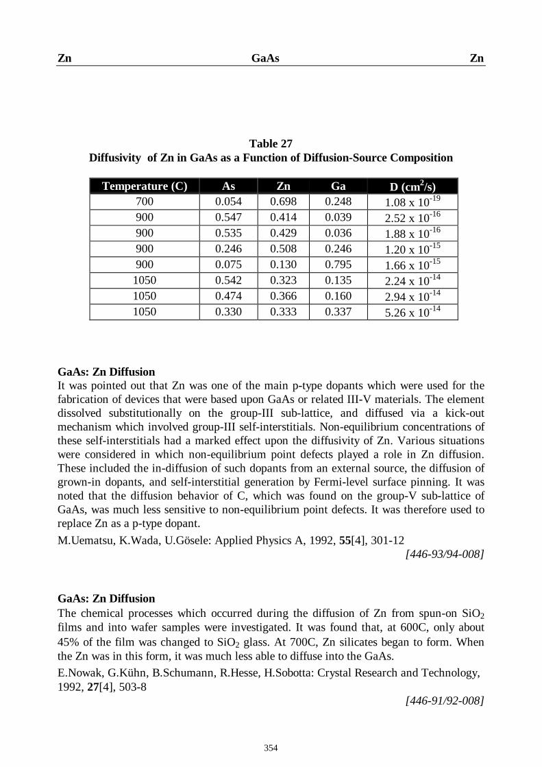
354
Zn GaAs Zn
Table 27Diffusivity of Zn in GaAs as a Function of Diffusion-Source Composition
Temperature (C) As Zn Ga D (cm2/s)700 0.054 0.698 0.248 1.08 x 10⁻¹⁹
900 0.547 0.414 0.039 2.52 x 10⁻¹⁶
900 0.535 0.429 0.036 1.88 x 10⁻¹⁶
900 0.246 0.508 0.246 1.20 x 10⁻¹⁵
900 0.075 0.130 0.795 1.66 x 10⁻¹⁵
1050 0.542 0.323 0.135 2.24 x 10⁻¹⁴
1050 0.474 0.366 0.160 2.94 x 10⁻¹⁴
1050 0.330 0.333 0.337 5.26 x 10⁻¹⁴
GaAs: Zn DiffusionIt was pointed out that Zn was one of the main p-type dopants which were used for thefabrication of devices that were based upon GaAs or related III-V materials. The elementdissolved substitutionally on the group-III sub-lattice, and diffused via a kick-outmechanism which involved group-III self-interstitials. Non-equilibrium concentrations ofthese self-interstitials had a marked effect upon the diffusivity of Zn. Various situationswere considered in which non-equilibrium point defects played a role in Zn diffusion.These included the in-diffusion of such dopants from an external source, the diffusion ofgrown-in dopants, and self-interstitial generation by Fermi-level surface pinning. It wasnoted that the diffusion behavior of C, which was found on the group-V sub-lattice ofGaAs, was much less sensitive to non-equilibrium point defects. It was therefore used toreplace Zn as a p-type dopant.M.Uematsu, K.Wada, U.Gösele: Applied Physics A, 1992, 55[4], 301-12
[446-93/94-008]
GaAs: Zn DiffusionThe chemical processes which occurred during the diffusion of Zn from spun-on SiO2films and into wafer samples were investigated. It was found that, at 600C, only about45% of the film was changed to SiO2 glass. At 700C, Zn silicates began to form. Whenthe Zn was in this form, it was much less able to diffuse into the GaAs.E.Nowak, G.Kühn, B.Schumann, R.Hesse, H.Sobotta: Crystal Research and Technology,1992, 27[4], 503-8
[446-91/92-008]

355
Zn GaAs Zn
GaAs: Zn DiffusionThe rapid thermal diffusion of Zn into semi-insulating material, from spun-on silica films,was investigated. Depending upon the heating rate, 2 types of secondary ion massspectrometry profile were observed.E.Nowak, G.Kühn, T.Morgenstern, B.Schumann: Crystal Research and Technology,1991, 26[8], 981-6
[446-88/89-014]
GaAs: Zn DiffusionThe migration of Zn into material which had been grown by means of molecular beamepitaxy at 200C was studied. The diffusion coefficient was found, using the sealedampoule technique, to be an order of magnitude higher in so-called low-temperaturematerial (1.3 x 10⁻¹¹cm2/s) than it was in normal material (1.5 x 10⁻¹²cm2/s). Thisdifference was attributed to the large number of defects (including As antisites) whichwere present in the low-temperature material. It was noted that the effectiveness of aSi3N4 diffusion mask depended upon whether the mask was deposited directly onto thelow-temperature material. A failure of such masks to stop Zn diffusion was attributed tothe effect of As atoms which out-diffused from the As-rich low-temperature material andinto the Si3N4. The presence of a 10nm GaAs layer on the low-temperature material waseffective in conserving the masking properties of the nitride.Y.K.Sin, Y.Hwang, T.Zhang, R.M.Kolbas: Journal of Electronic Materials, 1991, 20[6],465-70
[446-88/89-015]
GaAs: Zn DiffusionThe diffusion of Zn was studied by using liquid-phase epitaxy methods, and Si-doped n-type substrate material. The measurements were carried out at 850C, and dopantconcentrations which ranged from 1018 to 1019/cm3 were introduced. It was found that theZn concentration in the solid depended upon the square root of the atomic fraction of Znin the liquid. The diffusivity was dominated by the interstitial-substitutional process, andexhibited a cubic dependence upon the Zn content. The Zn interstitial was mainly doubly-ionized Zni
2+.C.Algora, G.L.Araujo, A.Marti: Journal of Applied Physics, 1990, 68[6], 2723-30
[446-86/87-002]
328 GaAs: Zn DiffusionThe migration of Zn in AlGaAs at 650C was studied by using the sealed-ampoule methodand a ZnAs2 source. It was found that the results for zero Al content (table 28) could bedescribed by the expression:
D (cm2/s) = 26 exp[-2.47(eV)/kT]V.Quintana, J.J.Clemencon, A.K.Chin: Journal of Applied Physics, 1988, 63[7], 2454-5
[446-72/73-003]

356
Zn GaAs Zn
Table 28Bulk Diffusivity of Zn in GaAs
Temperature (C) D (cm2/s)700 4.08 x 10⁻¹²
650 1.00 x 10⁻¹²
600 1.84 x 10⁻¹³
550 1.83 x 10⁻¹⁴
329 GaAs: Zn DiffusionIn order to study its diffusion mechanism, Zn was diffused from a ZnAs2 source into Si-doped samples, at temperatures ranging from 575 to 700C, in sealed evacuated quartztubes. The samples were characterized by means of the depth profile of thephotoluminescence at various temperatures. The photoluminescence spectra containedcharacteristic emissions which were associated with deep levels of Ga and As vacancies.A detailed analysis of the spectra revealed the role that was played by vacancies in the Zndiffusion process. A spatial correlation between the luminescence spectra, and the Znconcentrations deduced from secondary ion mass spectrometric data, was demonstrated. Itwas found that the data (table 29) could be described by the expression:
D(cm2/s) = 2.05 exp[-2.28(eV)/kT]N.H.Ky, L.Pavesi, D.Araujo, J.D.Ganière, F.K.Reinhart: Journal of Applied Physics,1991, 69[11], 7585-93
[446-86/87-012]
Table 29Diffusivity of Zn in GaAs
Temperature (C) D (cm2/s)700 3.33 x 10⁻¹²
650 7.12 x 10⁻¹³
600 1.72 x 10⁻¹³
575 5.43 x 10⁻¹⁴
GaAs: Zn DiffusionA marked difference between the Be and C distributions in this material was noted afterZn diffusion. It was shown that grown-in C was stable, and remained localized even afterZn diffusion. On the other hand, Be diffused very rapidly in the presence of diffusing Zn.

357
Zn GaAs Zn
This effect was attributed to differences in the crystal lattice sites which the dopantoccupied.E.Tokumitsu, T.H.Chiu, H.S.Luftman, N.T.Ha: Journal of Applied Physics, 1991, 69[12],8426-8
[446-86/87-013]
GaAs: Zn DiffusionThe Zn diffusion doping of GaAs, by using metalorganic vapor-phase epitaxy anddiethylzinc as a dopant source, was examined. Typical Zn concentrations and depthswhich were obtained were 1019 to 1021/cm3, and 40 to 200nm. The highest concentrationgradient which was obtained in this way was 4 orders of magnitude per 50nm, and thehighest Zn concentration was 2 x 10²¹/cm3 at the sample surface.Z.F.Paska, D.Haga, B.Willén, M.K.Linnarsson: Applied Physics Letters, 1992, 60[13],1594-6
[446-86/87-013]
GaAs: Zn DiffusionA simple method for the open-tube diffusion of Zn from (ZnO)x(SiO2)1-x film sources,and into GaAs was described. The oxide films were deposited by using metal-organicchemical vapor deposition. A capping layer of SiO2 was deposited on top of the sourcefilms, and diffusion was carried out in flowing N at 650C. Diffusion depths of between200nm and several microns could be easily obtained. The diffusion front in n-typesubstrates was sharp. The dependence of the diffusion depth upon the source filmcomposition (for x-values of 0.04 to 1) was determined by using sectioning methods.D.J.Lawrence, F.T.Smith, S.T.Lee: Journal of Applied Physics, 1991, 69[5], 3011-5
[446-78/79-002]
GaAs: Zn DiffusionRapid thermal annealing was used to diffuse Zn into GaAs from a thin-film zinc silicatesource that was prepared by chemical vapor deposition at atmospheric pressure.Comparisons were made with conventional open-tube furnace annealing, for a diffusiontemperature of 650C. The diffusivities were found to be similar; in contrast to previousresults. At temperatures ranging from 650 to 750C, sharp Zn diffusion profiles wereobserved. At temperatures above 750C, kinks in the diffusion profiles were found. Suchkinks were also observed when semi-insulating substrates were used instead of Si-dopedn+-type substrates. A model for Zn diffusion had already been developed, and this wasbased upon the pairing of interstitial Zn with all of the acceptor species which werepresent during diffusion. The predominant species were found to be substitutional Zn, andGa vacancies. The concentration of the latter was a function of the background dopantconcentration. The results of the model were shown to agree with all of the presentexperimental evidence, and were also consistent with the experimental observation of 2distinct activation energies for Zn diffusion into n+-doped substrates. These energies were

358
Zn GaAs Zn
equal to 1.1 and 2.6eV for temperatures which were above or below about 790C,respectively.G.Rajeswaran, K.B.Kahen, D.J.Lawrence: Journal of Applied Physics, 1991, 69[3],1359-65
[446-78/79-014]
330 GaAs: Zn DiffusionSamples were diffused with Zn, via a 200 to 300nm protective ZrO2 layer. The diffusiondepth exhibited a square-root time dependence. The absolute diffusivity values dependedslightly upon the diffusion conditions (table 30). The layer had essentially no effect uponthe carrier concentration profile or the activation energy.J.E.Bisberg, A.K.Chin, F.P.Dabkowski: Journal of Applied Physics, 1990, 67[3], 1347-51
[446-74-003]
Table 30Diffusivity of Zn in GaAs
Protection Source Temperature (C) D (cm2/s)ZrO2 Zn 755 3.8 x 10⁻¹¹
ZrO2 Zn 700 1.2 x 10⁻¹¹
ZrO2 Zn 650 6.9 x 10⁻¹²
ZrO2 Zn 600 1.3 x 10⁻¹²
ZrO2 GaAs/Zn2As3 650 2.0 x 10⁻¹²
- GaAs/Zn2As3 650 1.6 x 10⁻¹²
ZrO2 GaAs/Zn2As3 600 4.5 x 10⁻¹³
- GaAs/Zn2As3 600 3.8 x 10⁻¹³
- GaAs/Zn2As3 755 1.2 x 10⁻¹¹
- GaAs/Zn2As3 700 4.0 x 10⁻¹²
ZrO2 GaAs/Zn2As3 700 3.1 x 10⁻¹²
ZrO2 GaAs/Zn2As3 755 9.7 x 10⁻¹²
GaAs: Zn DiffusionThe saturation behavior of the free carrier concentrations in p-type GaAs monocrystalswhich had been doped by Zn diffusion was investigated. Free-hole saturation occurred at1020/cm3. The difference in saturation hole concentrations of materials was investigatedby studying the incorporation and lattice location of Zn. The latter was an acceptor whenlocated on a group-III atom site. Zinc was diffused into III-V wafers in a sealed quartzampoule. Particle-induced X-ray emission and ion-channelling techniques were then usedto determine the exact lattice location of Zn atoms. It was found that more than 90% ofthe Zn atoms occupied Ga sites in diffused GaAs samples. The results were analyzed interms of the amphoteric native defect model. It was shown that differences in the

359
Zn GaAs Zn
electrical activities of Zn atoms in various materials were a consequence of the differinglocations of the Fermi-level stabilization energy.L.Y.Chan, K.M.Yu, M.Ben-Tzur, E.E.Haller, J.M.Jaklevic, W.Walukiewicz,C.M.Hanson: Journal of Applied Physics, 1991, 69[5], 2998-3006
[446-78/79-015]
GaAs: Zn DiffusionThe use of thin Si films for the selective-area diffusion of Si and Zn was described. It wasfound that Si films behaved as ideal masks for Zn diffusion at temperatures below 750C.Ideal lateral Zn diffusion profiles were also observed when using these films; regardlessof the stress at the interface.G.A.Vawter, E.Omura, X.S.Wu, J.L.Merz, L.Coldren, E.Hu: Journal of Applied Physics,1988, 63[11], 5541-7
[446-72/73-003]
GaAs: Zn DiffusionThe growth and diffusion of abrupt Zn profiles in un-doped, or Si-doped, material wasmonitored by means of secondary ion mass spectrometry. The sharp diffusion frontswhich resulted from annealing treatments indicated that the Zn diffusion coefficient wasconcentration-dependent. The data were encompassed by the curves:
D(cm2/s) = 5.5 x 10⁻¹⁰ exp[-0.8(eV)/kT]and
D(cm2/s) = 1.8 x 10⁻⁹ exp[-1.0(eV)/kT]However, the diffusion of Zn at high concentrations appeared to be inhibited by crystaldefect kinetics and resulted in a relatively concentration-independent Zn diffusioncoefficient. The V/III growth ratio did not have any effect upon Zn diffusion in un-dopedor Si-doped material. The diffusion of Zn in heterojunction bipolar transistor structureswas different; in that the diffusion of Zn into a GaAs collector was larger by an order ofmagnitude, and decreased with an increase in the V/III growth ratio. In addition, thediffusion of Zn into an AlGaAs emitter was markedly lower and was inhibited by anincrease in the V/III ratio. These data could be summarized by the expressions:
GaAs (V/III = 60): D(cm2/s) = 2.0 x 10³ exp[-3.0(eV)/kT]GaAs (V/III = 120): D(cm2/s) = 1.0 x 10⁶exp[-3.6(eV)/kT]
Ga0.78Al0.22As (V/III = 60): D(cm2/s) = 6.8 x 10⁴ exp[-3.4(eV)/kT]Ga0.78Al0.22As (V/III = 120): D(cm2/s) = 1.1 x 10⁻⁵ exp[-1.7(eV)/kT]
P.Enquist, J.A.Hutchby, T.J.De Lyon. Journal of Applied Physics, 1988, 63[9], 4485-93[446-72/73-012]
GaAs: Zn DiffusionThe anomalous shape of Zn diffusion profiles in GaAs was quantitatively explained. TheFrank-Turnbull mechanism was suggested to govern interchanges, between interstitial andsubstitutional Zn, via Ga vacancies. It was proposed that these vacancies were eitherneutral or were singly ionized; depending upon the position of the Fermi level. In
360
Zn GaAs Zn
addition, 2 physical phenomena were proposed. Substitutional Zn thermally generatedinterstitial Zn-Ga vacancy pairs, and there was pairing between the donor (interstitial Zn)and the acceptor (substitutional Zn). The model furnished good agreement withexperimental data.K.B.Kahen: Applied Physics Letters, 1989, 55[20], 2117-9
[446-72/73-012]
GaAs: Zn DiffusionA review was presented of self-diffusion mechanisms and doping-enhanced superlatticedisordering. With regard to the influence of Zn p-type dopants, the Fermi level effect hadto be considered. In accord with its effect upon superlattice disordering, Zn diffusionappeared to be governed by the kick-out mechanism. It was concluded that dislocations inthis material and in other III-V compounds were only moderately efficient sinks orsources for point defects.T.Y.Tan, U.Gösele: Materials Science and Engineering, 1988, B1, 47-65
[446-62/63-208]
GaAs: Zn DiffusionThe diffusion of Zn into GaAs, from diethylzinc and trimethylarsenic, was studied. Theprocess produced surface hole concentrations which were greater than 1020/cm3. Well-controlled junction depths which could be as shallow as 0.000lmm were obtained, and asmooth surface morphology was retained. The profile shape was much more complexthan those predicted by accepted interstitial cum substitutional Zn diffusion models. Inorder to explain the observed profiles, a new model for Zn diffusion was proposed, andused in a computer simulation.S.Reynolds, D.W.Vook, J.F.Gibbons: Journal of Applied Physics, 1988, 63[4], 1052-9
[446-62/63-211]
GaAs: Zn DiffusionData were presented which showed that low-temperature (680C) Zn diffusion waseffective in reducing the dislocation density of epitaxial GaAs which was grown onto Si.The GaAs/Si system was analyzed by using both cross-sectional and plan-viewtransmission electron microscopy. Simple thermal annealing of GaAs/Si at a highertemperature (850C) was also studied. The reduction in dislocation density which occurreddue to Zn diffusion was suggested to arise from the increased concentrations of pointdefects which were generated during Zn diffusion. This resulted in enhanced dislocationclimb. The mechanism was consistent with impurity-induced layer disordering, via Zndiffusion, in AlGaAs/GaAs heterostructures.D.G.Deppe, N.Holonyak, K.C.Hsieh, D.W.Nam, W.E.Plano, R.J.Matyi, H.Shichijo:Applied Physics Letters, 1988, 52[21], 1812-4
[446-62/63-211]

361
Zn GaAs Zn
GaAs: Zn DiffusionSecond diffusion of Zn was observed using low concentrations. The behavior was similarto that of double diffusion in InP. The effect of the Zn activity in the vapor phase wasstudied by using a semi-closed box system. The observed Zn profiles were explained interms of a model which involved varying charge transfer by vacancy centers duringinterstitial-substitutional interchanges.K.Kazmierski, F.Launay, B.De Cremoux: Japanese Journal of Applied Physics, 1987,26[10], 1630-3
[446-55/56-007]
GaAs: Zn DiffusionA ternary Zn3As2-ZnAs2-GaAs source for the diffusion of Zn into GaAs was developedby using a low-temperature sintering technique. It was noted that wafers which werediffused by using this source remained free from damage. The dopant concentrations anddiffusion depths agreed with the results which were obtained by using high-temperatureGa/As/Zn diffusion sources.J.Werner, H.Melchior: Japanese Journal of Applied Physics, 1987, 26[4], 641-2
[446-51/52-117]
GaAs: Zn DiffusionA new method for self-aligned Si-Zn diffusion was described. In this method, closed-tubeSi diffusion was carried out by using a sputtered SiNx film. Then, Zn diffusion which wasself-aligned to the Si diffusion window was carried out by re-using the SiNx film as amask. The key factor was that the SiNx film should have the correct refractive indexprofile.W.X.Zou, R.Boudreau, H.T.Han, T.Bowen, S.S.Shi, D.S.L.Mui, J.L.Merz: Journal ofApplied Physics, 1995, 77[12], 6244-6
[446-121/122-045]
GaAs: Zn DiffusionThe isothermal diffusion of Zn was described in terms of the Longini reaction and arecombination process. It was assumed that, during diffusion, highly mobile Zninterstitials recombined with a Ga vacancy and became a relatively immobile site defect.It was noted that the long-term profile of the total Zn concentration was governed mainlyby the vacancy concentration profile. All of the known concentration profiles could beobtained for a constant diffusivity, without using fitting parameters. A new method wasproposed for determining the diffusivities of interstitial Zn, of Zn in Ga lattice sites, andof vacancies. These coefficients were deduced from existing experimental data. It wasshown that the apparent dependence of the Zn diffusivity upon its backgroundconcentration was due to its recombination with Ga vacancies.N.N.Grigorev, T.A.Kudykina: Fizika i Tekhnika Poluprovodnikov, 1997, 31[6], 697-702(Semiconductors, 1997, 31[6], 595-9)
[446-157/159-361]

362
Zn GaAs Zn
331 GaAs: Zn DiffusionThe diffusion of implanted Zn was studied, at annealing temperatures of between 625 and850C, by means of secondary ion mass spectrometry. A substitutional-interstitialdiffusion mechanism was proposed in order to explain how deviations of the local Gainterstitial concentration, from its equilibrium value, regulated Zn diffusion. It was foundthat it was possible to simulate both box-shaped profiles, that resulted from high-temperature annealing, and kink-and-tail profiles which resulted from lower-temperatureannealing. The simulation data permitted the determination of Arrhenius relationships forthe intrinsic diffusion coefficient of implanted Zn. This (table 31) could be described by:
D (cm2/s) = 0.6075 exp[-3.21(eV)/kT]M.P.Chase, M.D.Deal, J.D.Plummer: Journal of Applied Physics, 1997, 81[4], 1670-6
[446-148/149-172]
Table 31Diffusivity of Zn in GaAs
Temperature (C) D (cm2/s)850 1.9 x 10⁻¹⁵
800 1.2 x 10⁻¹⁵
800 6.0 x 10⁻¹⁶
750 1.2 x 10⁻¹⁶
750 8.4 x 10⁻¹⁷
675 8.4 x 10⁻¹⁸
675 3.1 x 10⁻¹⁸
GaAs: Zn DiffusionThe diffusion behavior was investigated by using a spun-on doped silica film. Diffusionannealing was carried out, at temperatures which ranged from 650 to 800C, using a SiO2
or Si3N4 cap. At higher temperatures, the sample surface after diffusion was found to bedamaged. The profiles which were obtained at temperatures ranging from 700 to 780Cwere of abrupt or kink-and-tail type. Diffusion annealing which was carried out using anitride cap were termed Ga-rich, and produced abrupt box-like profiles. The use of anoxide cap was expected to produce a superposition of shallow As-rich and deeper Ga-richprofiles; leading to a characteristic kink-and-tail profile. This behavior was observed athigher temperatures, but the junctions were too shallow to exhibit a tail at lowertemperatures. The junction depths were attributed to the existence of differing activationenergies for the two types of cap material. The energy that was required for oxide-capdiffusion was close to published values for oxide caps. The lower values which werefound for nitride-cap diffusion were closer to published values for a phosphosilicate glass

363
Zn GaAs Zn
cap. These results clearly showed that the nature of the cap material determined the typeof diffusion profile.S.Chatterjee, K.N.Bhat, P.R.S.Rao: Solid-State Electronics, 1997, 41[3], 496-500
[446-148/149-174]
GaAs: Zn DiffusionThe in-diffusion of Zn at high concentrations, under As-deficient conditions, caused thegeneration of dislocation loops, elongated dislocations and Ga precipitates decorated withvoids within the diffusion zone. Similar treatment under As vapor led to the recovery ofdiffusion-induced damage in the sub-surface region. This was accompanied by theappearance of 2 distinct steps in the Zn concentration profile. Previous work hadsuggested that these phenomena were connected with the out-diffusion of Ga fromprecipitates and towards the surface. The present results showed that the replacement, byP or Sb, of As in the diffusion ambient produced similar recovery effects.G.Boesker, H.G.Hettwer, A.Rucki, N.A.Stolwijk, H.Mehrer, W.Jaeger, K.Urban:Materials Chemistry and Physics, 1995, 42[1], 68-71
[446-136/137-110]
GaAs: Zn DiffusionThe diffusion of Zn, at high concentrations, into samples under As-deficient ambientconditions led to the generation of defects such as dislocation loops, elongateddislocations and Ga precipitates - decorated with voids- throughout the diffusion zone.Similar treatments under As vapor led to the recovery of diffusion-induced damage inregions beneath the surface. This was accompanied by the appearance of 2 distinct stepsin the Zn concentration profile. Previous work had suggested that these phenomena wereassociated with the out-diffusion of Ga from the precipitates and towards the surface. Itwas shown here that the replacement of As by P or Sb produced similar recovery effects.This indicated that ambient group-V elements made the near-surface of GaAs into aneffective sink for diffusion-induced excess Ga.G.Bösker, H.G.Hettwer, A.Rucki, N.A.Stolwijk, H.Mehrer, W.Jäger, K.Urban: MaterialsChemistry and Physics, 1995, 42[1], 68-71
[446-134/135-126]
GaAs: Zn DiffusionThe diffusivity of Zn in heavily-doped pnpn structures was measured after growth andannealing. During growth at 650C, the Zn diffusivity of about 10-12cm2/s in the buried p-type layer was found to be more than 10000 times the Zn diffusivity in the top p-typelayer. During annealing at 800C, the Zn diffusivity of about 5 x 10-14cm2/s in the buriedlayer remained orders of magnitude greater than the Zn diffusivity in the top layer. Themeasurements provided clear experimental evidence that a large flux of Ga interstitialswas injected from the surface during the growth of n-type layers, and that the Gainterstitials were trapped in the buried p-type layer by the electric field of the pn junctions(and were therefore positively charged). It was suggested that the resultant largeconcentration of Ga interstitials in the buried layer accounted for the increased Zn

364
Zn GaAs Zn
diffusivity via a kick-out mechanism. Finally, it was deduced that the mobile Zninterstitial was positively charged.C.Y.Chen, R.M.Cohen, D.S.Simons, P.H.Chi: Applied Physics Letters, 1995, 67[10],1402-4
[446-125/126-121]
GaAs: Zn DiffusionIt was recalled that the rapid diffusion of Zn into GaAs had recently been attributed to thefact that a small fraction of the Zn interstitials changed to Ga sites, thereby producinginterstitial Ga (IGa). This kick-out reaction led to the possibility of determining the IGa
transport properties from Zn diffusion experiments on essentially perfect GaAs. However,previous attempts had been impeded by the diffusion-induced generation ofmicrostructural defects which acted as IGa sinks. In the present study, this was preventedby using Zn-doped GaAs powder as a diffusion source. The measured 2-stage profilesshowed that, under these conditions, Zn diffusion at 906C was controlled by IGa
3+ inaddition to IGa
2+. Analysis of the profiles yielded quantitative data on the Ga- and Zn-related diffusivities, and on the concentration of IGa.G.Bösker, N.A.Stolwijk, H.G.Hettwer, A.Rucki, W.Jäger, U.Södervall: Physical ReviewB, 1995, 52[16], 11927-31
[446-125/126-121]
GaAs: Zn DiffusionThe Zn was diffused into GaAs through anodic oxide layers with various thicknesses anddensities. Electrochemical profiling was used to determine the electrically active Znconcentration and the diffusion depth. It was found that the depth of the junction variedinversely with the thickness and density of the oxide. However, the surface concentrationappeared to be independent of the oxide thickness or density and attained a value whichwas identical to that which was found for diffusion into a bare GaAs sample. The resultsdemonstrated that the most important effect of the oxide was to delay the introduction ofZn into the lattice. Thus, the anodic oxide could not be used as a mask or a Znconcentration attenuator.H.Cutlerywala, R.J.Roedel: Journal of the Electrochemical Society, 1994, 141[6], 1639-43
[446-119/120-192]
GaAs: Zn DiffusionThe Zn was introduced by using the electron beam doping method. That is, a Zn sheetwas sandwiched between GaAs wafers and the surface of the GaAs was irradiated with7MeV electrons. The use of secondary ion mass spectroscopy revealed U-shapeddiffusion profiles for impurities in the substrates. The results could be explained in termsof the kick-out mechanism, and surface diffusion processes.A.Takeda, T.Wada: Materials Science Forum, 1994, 143-147, 1421-6
[446-113/114-013]

365
Zn GaAs Zn
GaAs: Zn DiffusionSecondary ion mass spectroscopy and photoluminescence studies were made of VGaduring Zn diffusion into Si-doped material. Photoluminescence spectra were obtained atvarious etching depths below the sample surface. After annealing the samples in excessAs4 vapor at 650C, the conversion of n-type material into p-type material was observedby making electrical measurements in the region near to the sample surface. Theimportance of the SiGa-VGa emission band in photoluminescence spectra from thermallyconverted regions indicated that VGa which were generated at the surface duringannealing were responsible for the thermal conversion. The results also showed that themain point defects which were generated during annealing under Ga-rich conditions wereVAs and GaAs. In the case of Zn-diffused Si-doped substrates at 600C, the disappearanceof the VGa-related band from the photoluminescence spectra of diffused regions furnishedevidence for the incorporation of Zn interstitials into Ga sites during diffusion. Anaccumulation of VGa was found ahead of the Zn diffusion front. The Zn-diffused sampleswere also annealed at 800C for 2h in vacuum, or in As4 vapor with or without a Si3N4cap. In the case of samples which were annealed in vacuum, an abrupt diffusion frontadvanced slightly into the bulk; with a supersaturation of VGa ahead of the front. On theother hand, samples which were annealed in As vapor, with or without a cap on thesurface, exhibited double Zn concentration profiles with an undersaturation of VGa aroundthe tail region. These results revealed the important role which was played by non-equilibrium point defects, and were explained in terms of a kick-out mechanism for Zndiffusion.N.H.Ky, J.D.Ganière, F.K.Reinhart, B.Blanchard: Materials Science Forum, 1994, 143-147, 1397-402
[446-113/114-014]
GaAs: Zn DiffusionExperimental studies were made of Zn diffusion, using high temperatures, open tubes,and SiO2 protective layers. Precisely controlled diffusion depths of less than 0.2 or 0.4µcould be obtained by using SiO2, doped with 0.1%Zn, as a diffusion source. Under theseconditions, the diffusion coefficients were equal to 1.31 x 10⁻¹³ and 1.76 x 10⁻¹²cm2/s attemperatures of 700 and 1025C, respectively.D.K.Gautam, Y.Shimogaki, Y.Nakano, K.Tada: Materials Science Forum, 1993, 117-118, 417-22
[446-111/112-051]
GaAs: Zn DiffusionAfter Zn diffusion into Si-doped material, the diffused samples were annealed in vacuum,in As vapor, or with a Si3N4 mask capping the surface. The Zn concentration profileswhich were obtained by secondary ion mass spectroscopy, and photoluminescence spectrafor various depths below the sample surface, were studied in detail. After annealing invacuum, the steep (p+-n) Zn diffusion front advanced into the bulk. It was observed that
366
Zn GaAs Zn
the intensity ratio between the Si donor-Ga vacancy complex (SiGa-VGa) related emissionband and the band-to-band (e-h) transition was enhanced in the region ahead of the Zndiffusion front. On the other hand, Zn atoms diffused deeper into the bulk of sampleswhich were annealed in As vapor, with or without a capping layer. These samplesexhibited kink-and-tail (p+-p-n ) Zn concentration profiles with a decrease in the intensityratio around the tail region. Analysis of the photoluminescence data suggested that therewas a supersaturation of Ga vacancies ahead of the diffusion front of samples which wereannealed in vacuum, and an under-saturation of this defect around the tail region ofsamples which were annealed in As vapor. The results emphasized the important rolewhich was played by non-equilibrium of the defect concentration during post-diffusionannealing. This permitted an anomalous Zn double profile to be explained in terms of theinterstitial-substitutional mechanism.N.H.Ky, J.D.Ganière, F.K.Reinhart, B.Blanchard, J.C.Pfister: Journal of Applied Physics,1993, 74[9], 5493-500
[446-111/112-051]
GaAs: Zn DiffusionThe microscopic mechanisms of Zn diffusion in GaAs were investigated by using abinitio molecular dynamics techniques. It was found that, among the various proposedmechanisms for Zn diffusion, kick-out by Ga interstitials had the lowest activationenergy. The occurrence of Zn in-diffusion generated non-equilibrium group-IIIinterstitials which were bound to Zn by Coulomb forces. The interstitials followed the Zndiffusion front and disordered the superlattice. The calculated activation energies forthese processes were in good agreement with experimental data.C.Wang, Q.M.Zhang, J.Bernholc: Physical Review Letters, 1992, 69[26], 3789-92
[446-106/107-039]
GaAs: Zn DiffusionThe electrical activity and lattice-site locations of Zn atoms which had been diffused intoGaAs were studied by using various characterization techniques. Particle-induced X-rayemission channelling showed that all of the Zn atoms were substitutional and wereelectrically active acceptors. A difference between the behaviors of Zn in GaAs and InPcould be understood in terms of the amphoteric native defect model. It was also shownthat the Fermi level stabilization energy provided a convenient energy reference for thetreatment of dopant diffusion at semiconductor hetero-interfaces.W.Walukiewicz, K.M.Yu, L.Y.Chan, J.Jaklevic, E.E.Haller: Materials Science Forum,1992, 83-87, 941-6
[446-99/100-065]
GaAs: Zn DiffusionA model was developed which could explain the nature of Zn diffusion profiles in n+-typematerial. The model was based upon the effect of Coulomb pairing between interstitialand substitutional Zn. By extending the model so as to include the Coulomb pairing ofinterstitial Zn with all of the acceptors which were present during diffusion, the

367
Zn GaAs Zn
predictions were caused to be in good agreement with experimental data. Only oneadjustable parameter was involved.K.B.Kahen, J.P.Spence, G.Rajeswaran: Journal of Applied Physics, 1991, 70[4], 2464-6
[446-91/92-008]
GaAs/AlAs: Zn DiffusionThe microscopic mechanisms of Zn-induced interdiffusion in GaAs/AlAs superlattices,were investigated by using ab initio molecular dynamics techniques. It was found that,among the various proposed mechanisms for Zn diffusion, kick-out by Ga interstitials hadthe lowest activation energy. The occurrence of Zn in-diffusion generated non-equilibrium group-III interstitials which were bound to Zn by Coulomb forces. Theinterstitials followed the Zn diffusion front and disordered the superlattice. The calculatedactivation energies for these processes were in good agreement with experimental data.C.Wang, Q.M.Zhang, J.Bernholc: Physical Review Letters, 1992, 69[26], 3789-92
[446-106/107-039]
GaAs/AlAs: Zn DiffusionA model was proposed for the effect of Zn in-diffusion in enhancing superlatticedisordering. It combined recently proposed models for Ga self-diffusion and Zn diffusionin GaAs. Four coupled partial differential equations, which described the process, weresolved numerically. Satisfactory agreement was obtained between the simulated resultsand published experimental data. At a given temperature, and for the values which wereassumed for the diffusion coefficient and thermal equilibrium concentration of pointdefects, doubly positively charged Ga self-interstitials, IGa
2+, were deduced to be aconsistent splitting of the known Ga self-diffusion coefficient which was dominated byIGa
2+. The superlattice disordering enhancement was due mainly to the Fermi-level effect,but IGa
2+ supersaturation also made a small contribution. Because of p-doping by Znacceptor atoms, the IGa
2+ concentration was greatly increased via the Fermi-level effect.An IGa
2+ supersaturation also developed because the IGa2+ generation rate was higher than
its removal rate. Enhanced superlattice disordering occurred mainly under Ga-richsuperlattice conditions. The Zn in-diffusion enhanced Al-Ga interdiffusion coefficientexhibited an apparent dependence, upon the Zns
- concentration, which differed slightlyfrom a quadratic relationship.H.Zimmermann, U.Gösele, T.Y.Tan: Journal of Applied Physics, 1993, 73[1], 150-7
[446-106/107-078]
GaAs/AlAs: Zn DiffusionThe Car-Parrinello method was used to study Zn-enhanced interdiffusion in superlattices.The energetics of several mechanisms for the diffusion of Zn were examined. It wasfound that a pair which consisted of a substitutional Zn acceptor and an interstitial group-III atom had a substantially lower formation energy than did an isolated interstitial. Thelow formation energy of this pair resulted in the interstitial kick-out mechanism having amuch lower activation energy than those which involved vacancies or the dissociative
368
Zn GaAs Zn
(Frank-Turnbull or Longini) mechanism. The lowest-energy path for the interchange ofgroup-III atoms involved the kick-out of Zn by a group-III interstitial, followed by fast Zninterstitial diffusion and the subsequent ejection of another group-III atom into theinterstitial channel. The activation energies for these processes, as determined byfollowing the kick-out trajectories and including full relaxation of all of the atoms, werein good agreement with experimental data.Q.M.Zhang, C.Wang, J.Bernholc: Materials Science Forum, 1992, 83-87, 1351-6
[446-99/100-083]
GaAs/AlGaAs: Zn DiffusionMultiple quantum well structures, with the same well thickness but differing AlxGa1-xAscompositions (with x = 0.1, 0.2, 0.45, or 1), were grown by using molecular beamepitaxy. After Zn diffusion at 575C (1 to 16h), the structures were studied by means ofthe transmission electron microscopy of cleaved wedges, secondary electron imaging in ascanning electron microscope, and by means of secondary ion mass spectroscopy. Theresults showed that totally and partially disordered regions always lay beyond the Zndiffusion front. The extent of partial disordering depended upon the value of x. As xincreased, the disordering rate increased due to an increase in Zn diffusivity. The effect ofa high Zn concentration was investigated by monitoring the photoluminescence andRaman scattering. Analysis of the photoluminescence spectra of structures which hadbeen diffused for various times, and of the photoluminescence spectra from variousdepths below the sample surface, made it possible to describe the physical processeswhich occurred during Zn diffusion. Column-III vacancies were created at the samplesurface and diffused into the bulk of the sample, where they were filled by other defects.By using X-ray diffraction techniques, an expansion of the lattice constant in the regionbeyond the Zn diffusion front was detected. This was attributed to a supersaturation ofcolumn-III interstitials. During the incorporation of Zn into the crystal lattice, column-IIIinterstitials were generated. These were suggested to be responsible for the enhancementof Al-Ga interdiffusion. An important role was played by the electric field at the p-njunction that was formed by Zn diffusion. That is, the negatively charged column-IIIvacancies and the positively charged column-III interstitials were confined to the n and psides of the p-n junction, respectively. These results provided evidence for a self-interstitial mechanism of Zn diffusion-induced disordering in these multiple quantum wellstructures.N.H.Ky, J.D.Ganière, M.Gailhanou, B.Blanchard, L.Pavesi, G.Burri, D.Araújo,F.K.Reinhart: Journal of Applied Physics, 1993, 73[8], 3769-81
[446-106/107-079]
GaAs/AlGaAs: Zn DiffusionAn investigation was made of the diffusion of Zn in n-GaAs/Zn-AlGaAs/Se-AlGaAsstructures during the growth of n-GaAs layers which were doped with Se and Si. It wasfound that the diffusion of Zn in these structures depended strongly upon the type ofdopant as well as upon the carrier concentration in the n-GaAs layer. The amount of Znwhich diffused into both n-GaAs and Se-AlGaAs layers was much smaller for a Si-doped
369
Zn GaAs Zn
GaAs layer than for a Se-doped layer. The slower diffusion which occurred during thegrowth of Si-doped GaAs layers in these structures could be reasonably well explained bymodifying a model in which interstitial Ga which diffused from the n-GaAs layer and intothe Zn-AlGaAs layer was supposed to kick out substitutional Zn. The density ofinterstitial Ga in the Si-doped GaAs layer could be lower than in the Se-doped GaAsbecause the interstitial Ga atoms replaced Si which occupied the column-III site. This wasnot the case for Se-doped GaAs, where Se occupied the column-V site.N.Fujii, T.Kimura, M.Tsugami, T.Sonoda, S.Takamiya, S.Mitsui: Journal of CrystalGrowth, 1994, 145[1-4], 808-12
[446-119/120-201]
GaAs/GaAlAs: Zn DiffusionHeterostructures of GaAs/Ga0.7Al0.3As, which contained Zn and Se as intrinsic p and ndopants, were subjected to combined Be and O implantation. Rapid thermal annealingthen resulted in the enhanced out-diffusion of Zn. The Se dopant profile remainedessentially unchanged. The atomic profile of Zn could be related to the microscopicdefect distributions. A change in the photoluminescence spectrum, due to over-compensation of the n-doped GaAs and GaAlAs layers, was observed. Annealing withoutpreceding implantation had no effect upon the Zn atomic profile.T.Humer-Hager, R.Treichler, P.Wurzinger, H.Tews, P.Zwicknagl: Journal of AppliedPhysics, 1989, 66[1], 181-6
[446-74-026]
GaAs/GaAlAs: Zn DiffusionMultiple quantum-well GaAs/Ga0.8Al0.2As structures which were uniformly Si-doped, toconcentrations ranging from 1017 to 1019/cm3, were grown by means of molecular-beamepitaxy in order to study the effects of the background Si dopant level upon the Zndiffusion-induced disordering. After Zn diffusion (575C, 4 or 16h), cleaved wedges of thesamples were investigated by means of secondary-ion mass spectrometry andtransmission electron microscopy. The results showed that completely and partiallydisordered regions were always behind the Zn diffusion front. A dependence of theeffective Zn diffusivity and of the disordering rate of the structure upon the backgroundSi dopant level was observed. The effective Zn diffusivity and the disordering ratesignificantly decreased with increasing background Si concentration. Before Zn diffusion,the photoluminescence spectra of Si-doped structures exhibited an increase in intensity ofthe Si donor column-III vacancy complex emission band with increasing Si dopant level.This indicated that the concentration of column-III vacancies in the structures increasedas the background Si concentration was increased. After Zn diffusion, a large decrease inintensity of the column-III vacancy-related emission band was observed in thephotoluminescence spectra from Zn-diffused regions. A model that was based upon theso-called kick-out mechanism of Zn diffusion was proposed in order to explain the effectof the background Si doping level upon the effective Zn diffusivity. The model showedthat the effective Zn diffusivity was controlled by the concentration of column-IIIinterstitials behind the Zn diffusion front, and by the donor concentration in the sample.

370
Zn GaAs Muons
Column-III interstitials were generated during the incorporation of Zn into the crystallattice. The supersaturation of these interstitials behind the Zn diffusion front wasresponsible for the enhancement of Al-Ga interdiffusion. Because column-III interstitialsand column-III vacancies could mutually annihilate, the concentration of column-IIIinterstitial and column-III vacancies in Zn-diffused regions decreased with increasing Sidoping level; thus leading to a retardation of Zn diffusion into the structure. A decrease ineffective Zn diffusivity, caused by an increase in the donor concentration of the samples,was also demonstrated. The results revealed effects of the Fermi level and of interactionsbetween point defects during the Zn diffusion-induced disordering of GaAs/AlGaAsmulti-layered structures.N.H.Ky, J.D.Ganière, F.K.Reinhart, B.Blanchard: Journal of Applied Physics, 1996,79[8], 4009-16
[446-134/135-136]
GaAs/GaAlAs: Zn DiffusionSecondary-ion mass spectrometry and photoluminescence methods were used to study Zndiffusion into GaAs/Ga0.8Al0.2As multi quantum-well structures which were uniformlydoped with Si to concentrations of between 1017 and 1019/cm3. The secondary-ion massspectrometry profiles which were measured after Zn diffusion at 575C revealed a largeeffect of the background Si doping level upon the Zn diffusion process and upon Zndiffusion-induced disordering of the multi quantum-well structures. It was found that theZn diffusivity and the disordering rate significantly decreased with increasing Sibackground concentration. Before Zn diffusion, the photoluminescence spectra of themulti quantum-well samples revealed an increased intensity of the Si donor-VIII complexemission band with increased Si doping level. This indicated that the VIII concentration inthe multi quantum-well structures increased as the Si background concentration increased.After Zn diffusion, a large decrease in the intensity of the VIII-related emission band wasdetected in the photoluminescence spectra which were obtained from Zn-diffused regions.The results were explained in terms of the kick-out mechanism of Zn diffusion. Duringthe incorporation of Zn into the crystal lattice, column-III interstitials were generated. Thesupersaturation of IIII behind the Zn diffusion front resulted in an enhancement of Al-Gainterdiffusion in the Zn-diffused region. Since IIII and VIII could mutually annihilate, areduction in IIII concentration occurred in the Zn-diffused region of Si-doped sampleswhich contained a high VIII concentration. As a result, Zn diffusion and disordering of themulti quantum-well structures were retarded with increasing Si-doping level.N.H.Ky: Materials Science Forum, 1995, 196-201, 1643-8
[446-127/128-139]
Muons
GaAs: Muon DiffusionMeasurements were made of the dynamics of negatively charged muonium in heavily Si-doped material at temperatures ranging from 295 to 1000K. The muonium began to

371
Muons GaAs Muons
diffuse, at temperatures above 500K, at a hopping rate which was described by an attemptfrequency of 5.6 x 10¹²/s and an activation energy of 0.73eV. At temperatures above700K, relaxation from charge-state fluctuations was observed. The data implied that Mu-
to Muo conversion occurred, via the alternating capture of holes and electrons. Thisestablished that Mu was a deep recombination center. Similar dynamics were expectedfor the isolated H- center in n-type material.K.H.Chow, B.Hitti, R.F.Kiefl, S.R.Dunsiger, R.L.Lichti, T.L.Estle: Physical ReviewLetters, 1996, 76[20], 3790-3
[446-136/137-111]
GaAs: Muon DiffusionThe results of investigations of transitions among the sites and charge states of muoniumwere summarized. Energy parameters were determined for the full description ofmuonium dynamics and were found to correlate well with available data for H. A modelwas developed which accounted for all of the major features which were observed. Itsvalidity for a wide range of dopant concentrations, using a single set of parameters,reflected its predictive strength. The near equality of the energy parameters for muoniumas compared with those which were available for H, strongly implied that the results formuonium dynamic behavior should be applicable to H, with very little change. The modelcould be applied to all tetrahedrally coordinated semiconductors, with few modifications,and served as a basis for the understanding of muonium dynamics in GaAs and othermaterials. Differences in H properties could be understood by examining material-specific deviations from the basic model.R.L.Lichti, C.Schwab, T.L.Estle: Materials Science Forum, 1995, 196-201, 831-6
[446-127/128-119]
GaAs: Muon DiffusionIt was noted that the presence of Si donors had a marked effect upon the charge state anddiffusion of muonium at the tetrahedral interstitial site (MuT
o), while it had a relativelyweak effect upon bond-center muonium (MuBC
o). In metallic Si-doped material, thehighly mobile MuT
o center which was observed in non-metallic material was replaced bya charged species (probably Mu-) which had a diffusion rate that was smaller than that ofthe MuT
o center. The MuBCo center was metastable, and its transition to MuT
o or Mu-
centers (depending upon dopant concentration) was observed at 50 to 150K. The resultsalso suggested that the MuT
o state underwent fast spin-exchange interaction withconductive carriers before the transition: MuT
o → Mu-.R.Kadono, A.Matsushita, K.Nagamine, K.Nishiyama, K.H.Chow, R.F.Kiefl,A.MacFarlane, D.Schumann, S.Fujii, S.Tanigawa: Physical Review B, 1994, 50[3], 1999-2002
[446-115/116-118]

372
Muons GaAs General
GaAs: Muon DiffusionBy measuring the muon spin relaxation rate of muonium as it moved from site to site in ahost lattice with nuclear spins, it was possible to derive an average correlation time, t , forfluctuations in the nuclear hyperfine field which acted upon the unpaired electron.Provided that the motion was incoherent (diffusive), t was inversely proportional to thediffusion constant. Such measurements were reported here for isotropic muonium attemperatures ranging from 20mK to 300K. Large differences were found in the muoniummotion, and were most marked at low temperature; where l/t became temperature-independent below about 10K in GaAs. A study was also made of the diffusive behaviorof muonium in various GaAs samples in order to detect the possible effect of slightcrystalline imperfections.W.Schneider, R.F.Kiefl, E.J.Ansaldo, J.H.Brewer, K.Chow, S.F.J.Cox, S.A.Dodds,R.C.Duvarney, T.L.Estle, E.E.Haller, R.Kadono, S.R.Kreitzman, R.L.Lichti,C.Niedermayer, T.Pfiz, T.M.Riseman, C.Schwab: Materials Science Forum, 1992, 83-87,569-74
[446-99/100-065]
General
GaAs: DiffusionA review was presented of developments in the understanding of self-diffusion andimpurity diffusion processes in this material; with particular emphasis being placed on theinclusion of recent Ga-isotope diffusion data. Specific diffusion mechanisms weresuggested for C, P, Sb and S; which were all substitutionally dissolved on the As sub-lattice.U.Gösele, T.Y.Tan, M.Schultz, U.Egger, P.Werner, R.Scholz, O.Breitenstein: Defect andDiffusion Forum, 1997, 143-147, 1079-94
[446-143/147-1079]
GaAs[l]: ElectromigrationA new experimental technique was proposed which permitted the measurement of theeffective mobility of solute elements in III-V solutions. It was based upon the concept ofan electro-epitaxial growth experiment in which the Peltier effect contribution to growthwas eliminated by adjusting the current flow direction so that it was parallel to thesubstrate surface. Thus, only diffusion and electrotransport contributed to growth.Z.R.Zytkiewicz: Journal of Crystal Growth, 1987, 82[4], 647-51
[446-55/56-168]
GaAs: DiffusionDuring the fabrication of refractory gate MESFET devices, sputter deposition of a WSix
gate and reactive ion etching of the gate pattern could lead to surface damage andcontamination. In order to study these effects, material with a shallow Si implant was

373
General GaAs General
subjected to reactive ion etching alone, or to both WSix sputter deposition and reactiveion etching, before annealing. The surface damage, due to WSix sputter deposition andreactive ion etching at self-bias under 200V, was healed by capped (SiNx) furnaceannealing at 800C. It was found that sheet resistance and Hall mobility measurementscould be correlated with the diffusion of compensating impurities into the bulk.Secondary ion mass spectrometry profiles indicated that the major contaminants (Fe, Cr,Ni, Cu, V) were already present in the W targets and were thus present in the WSix
layers. These contaminants were left on the surface of the GaAs after gate reactive ionetching and were driven into the bulk during capped annealing. An HCl etch was found toremove the contaminants; thus resulting in lower sheet resistances for implanted andprocessed GaAs. Refractory gate sub-micron MESFET devices which were fabricated byusing an HCl etch after gate reactive ion etching exhibited a reduced access resistance.H.Baratte, A.J.Fleischman, G.J.Scilla, T.N.Jackson, H.J.Hovel, F.Cardone: Journal of theElectrochemical Society, 1991, 138[1], 219-22
[446-78/79-010]
GaAs: DiffusionA long-term reliable spun-on source was developed for open-tube p+ diffusion into III/Vcompound semiconductors. The source consisted of an aqueous/alcoholic solution ofzircon alcoholate, doped with zinc chloride. After spinning and drying in air at 300C, aglassy film of ZrO2:ZnO on the semiconductor surface acted as a solid-state source forsubsequent diffusion. This solution exhibited an excellent long-term durability.Furthermore, the thermal expansion coefficient of zirconia was well matched to that ofmost III/V compound semiconductors and yielded very stable films, even at hightemperatures. This permitted essentially stress-free diffusion. Diffusion into GaAs wascarried out at temperatures ranging from 600 and 700C. The hole concentrations anddiffusion coefficients which were obtained by using this source were rather close to thoseobtained by using other diffusion techniques. The simpler handling and long-termdurability of zirconia-based solutions offered significant advantages over other p+-diffusion techniques which were used in the preparation of III/V compoundsemiconductors.G.Franz, M.C.Amann: Journal of the Electrochemical Society, 1989, 136[8], 2410-3
[446-70/71-105]
GaAs: DiffusionDeep-level transient Fourier spectroscopic, Hall-effect and DSL etching techniques wereused to analyze initially semi-insulating bulk samples after annealing at temperatures ofbetween 800 and 1100C under As pressures of between 0 and 3bar. It was found that theelectrical resistivity, electronic mobility and EL2 concentration increased with increasingAs pressure at all temperatures. Initially n-type samples were converted to p-type atpressures below 0.5bar and temperatures above 1000C. It was noted that As precipitatesdisappeared at high temperatures, and reappeared during low temperature annealing. Inorder to explain the observations, it was proposed that long-range rapid As interstitialtransport occurred between the surface and the bulk, together with short-range Ga

374
General GaAs Surface
vacancy migration involving dislocations as sources and sinks. It was suggested that adiscrepancy, with regard to very small reported tracer diffusion coefficients, could beresolved by assuming that rapidly diffusing marked interstitials which entered the latticeat the crystal surface tended to exchange sites with unmarked lattice species. They thenbecame immobile.M.Noack, K.W.Kehr, H.Wenzl: Journal of Crystal Growth, 1997, 178, 438-44
[446-152-0374]
Surface Diffusion
Al
GaAs: Al Surface DiffusionDuring the molecular beam epitaxial growth of GaAs on the vicinal (100) surface ofGaAs, reflection high-energy electron diffraction was used to measure the transitiontemperature between 2-dimensional nucleation and pure step propagation which occurredwhen sub-monolayer amounts of Sn were present on the surface. In the case of sampleswhich were misoriented by 0.5º with respect to the [011] or [011] direction, the transitiontemperature decreased by approximately 100C after the deposition of 0.6 of a monolayerof Sn. The presence of Sn increased the surface mobility of Al adatoms on (100) AlAssurfaces; as indicated by the annealing behavior of the AlAs surface at 600C.G.S.Petrich, A.M.Dabiran, P.I.Cohen: Applied Physics Letters, 1992, 61[2], 162-4
[446-93/94-001]
GaAs: Al Surface DiffusionMisoriented samples which were tilted by 1 or 2º away from the (001) plane and towards[110] or (111), or towards [110] or (111), were prepared. The critical temperature atwhich a transition in growth mode occurred was studied by using reflection high-energyelectron diffraction methods during the growth of AlAs on GaAs vicinal surfaces. Thecritical temperature of AlAs was higher than that of GaAs, thus indicating that the step-flow growth of AlAs occurred at a higher temperature. By combining these data with atheory that took account of 2-dimensional nucleation and surface diffusion, the surfacediffusion length of Al was deduced. It was found to be greater than that of Ga for bothtypes of substrate surface. By taking account of chemical equilibrium at the step edge ofeach surface, it was predicted that the surface diffusion length of Al should beanisotropic.M.Tanaka, T.Suzuki, T.Nishinaga: Japanese Journal of Applied Physics, 1990, 29[5],L706-8
[446-76/77-006]
GaAs: Al Surface DiffusionThe adsorption and migration characteristics of Al atoms on (100) surfaces wereinvestigated by using reflection high-energy electron diffraction and the alternate
375
Surface GaAs Surface
deposition of Al and As4 onto the growing surface. All of the results were attributed tothe existence of differing migration velocities for various atoms.Y.Horikoshi, H.Yamaguchi, M.Kawashima. Japanese Journal of Applied Physics, 1989,28[8], 1307-11
[446-72/73-001]
As
GaAs: As Surface DiffusionThe incorporation diffusion length of surface-migrating adatoms on molecular beamepitaxial material was studied theoretically and experimentally. By using microprobereflection high-energy electron diffraction and scanning electron microscopic techniques,it was demonstrated that the incorporation diffusion length depended strongly upon theAs partial pressure, and was of the order of 1µ. This behavior was explained by assumingthat the Ga flux which entered the step exceeded the As flux. When the Ga flux whichentered the step was lower than that of As, the incorporation diffusion length decreased tothat of the step separation; and was then typically of the order of tens of nm. It wasconcluded that the balance of Ga and As fluxes which entered the step edge determinedthe incorporation diffusion length of Ga.T.Nishinaga, X.Q.Shen: Applied Surface Science, 1994, 82-83, 141-8
[446-123/124-161]
Ga
GaAs: Ga Surface DiffusionDuring the molecular beam epitaxial growth of GaAs on the vicinal (100) surface ofGaAs, reflection high-energy electron diffraction was used to measure the transitiontemperature between 2-dimensional nucleation and pure step propagation which occurredwhen sub-monolayer amounts of Sn were present on the surface. In the case of sampleswhich were misoriented by 0.5º with respect to the [011] or [011] direction, the transitiontemperature decreased by approximately 100C after the deposition of 0.6 of a monolayerof Sn. This indicated that the Ga mobility had increased.G.S.Petrich, A.M.Dabiran, P.I.Cohen: Applied Physics Letters, 1992, 61[2], 162-4
[446-93/94-001]
GaAs: Ga Surface DiffusionThe dependence of Ga adatom surface diffusion upon the As flux during molecular beamepitaxial growth was investigated. Variations of the growth rate of GaAs layers, grownonto (001) surfaces adjacent to (111) surfaces, were measured by means of scanningmicroprobe reflection high-energy electron diffraction. The surface diffusion length was
376
Surface GaAs Surface
deduced from the variations in the growth rate. It was found that the surface diffusionlength of the Ga adatoms became larger under a lower As flux.M.Hata, A.Watanabe, T.Isu: Journal of Crystal Growth, 1991, 111[1-4], 83-7
[446-91/92-007]
GaAs: Ga Surface DiffusionThe microscopic details of Ga adatom diffusion upon an As-stabilized (001) surface wereinvestigated by using an ab initio pseudopotential method. The results showed that Gaadatoms diffused on the surface by passing through the missing As dimer rows. Acomparison with scanning tunnelling microscopic experiments during molecular beamepitaxial growth suggested that a low pressure of As increased surface Ga adatomdiffusion due to the creation of a continuous Ga adatom diffusion path. This conclusionwas consistent with the observation that low-temperature growth was possible viamigration-enhanced epitaxy in which As and Ga sources were supplied alternately.K.Shiraishi: Applied Physics Letters, 1992, 60[11], 1363-5
[446-86/87-010]
GaAs: Ga Surface DiffusionMisoriented samples which were tilted by 1 or 2º away from the (001) plane and towards[110] or (111), or towards [110] or (111), were prepared. The critical temperature atwhich a transition in growth mode occurred was studied by using reflection high-energyelectron diffraction methods during the growth of AlAs on GaAs vicinal surfaces. Thecritical temperature of AlAs was higher than that of GaAs, thus indicating that the step-flow growth of AlAs occurred at a higher temperature. The surface diffusion length of Gawas found to be shorter than that of Ga for both types of substrate surface.M.Tanaka, T.Suzuki, T.Nishinaga: Japanese Journal of Applied Physics, 1990, 29[5],L706-8
[446-76/77-006]
GaAs: Ga Surface DiffusionAn experimental study of RHEED intensity oscillations was performed on (111)Bsubstrates which were misoriented by 1 or 2º towards [110], [211], or [211] orientations.The behavior of the RHEED oscillations on (111)B was similar to that on (001).However, the temperature at which the RHEED intensity oscillations began to appear on(111)B was lower than that on (001). The surface diffusion length of Ga on (111)B wasevaluated by taking account of the supersaturation ratio of adatoms on the terrace.T.Shitara, E.Kondo, T.Nishinaga: Journal of Crystal Growth, 1990, 99, 530-4
[446-76/77-008]
GaAs: Ga Surface DiffusionSurface diffusion during molecular beam epitaxy was studied. Firstly, the mode transitionbetween 2-dimensional nucleation and step flow during molecular beam epitaxial growthon vicinal surfaces was studied theoretically and experimentally. The basis of the theorywas to assume that the transition occurred when the surface supersaturation on the step

377
Surface GaAs Surface
terrace became identical to the critical supersaturation for 2-dimensional nucleation. Thispermitted the diffusion length of Ga to be calculated at the experimentally determinedcritical temperature for the mode transition. It was found that the diffusion lengthincreased, as the temperature decreased, due to an increased residence time. Also, thediffusion length on (111)B was longer than that on (001) when the same formation energyfor 2-dimensional nuclei was assumed for both surfaces. The theory gave good agreementwith the experimental data, and it was concluded that surface diffusion was one of themost important processes which controlled molecular beam epitaxial growth and impurityincorporation.T.Nishinaga, T.Shitara, K.Mochizuki, K.I.Cho: Journal of Crystal Growth, 1990, 99, 482-90
[446-76/77-009]
GaAs: Ga Surface DiffusionThe adsorption and migration characteristics of Ga atoms on (100) surfaces wereinvestigated by using reflection high-energy electron diffraction and the alternatedeposition of Ga and As4 onto the growing surface. Excess Ga deposition onto the surfaceproduced Ga clusters or droplets on the first Ga layer. These dissolved very quickly afterAs4 deposition and formed flat GaAs layers when the number of Ga atoms was near to 2or 3 times the surface site number. All of the results were attributed to the existence ofdiffering migration velocities for various atoms.Y.Horikoshi, H.Yamaguchi, M.Kawashima. Japanese Journal of Applied Physics, 1989,28[8], 1307-11
[446-72/73-001]
GaAs: Ga Surface DiffusionThe generation of extra facets on ridge-type triangles, with (001)-, (110)- and (201)-related equivalent slopes on GaAs (111) A substrates, and stripes running in [110], [110]and [100] directions on (001) substrates, was investigated during the molecular beamepitaxy of GaAs/AlGaAs multi-layers. By investigating local variations in the layerthickness in regions adjacent to extra (114)A, (110) and (111)B facets which werecommon to the (111)A and (001) patterned substrates, and extra facets which were relatedto the respective substrates and growth rates of the facets relative to the growth rate onthe substrate plane, the orientation-dependent Ga surface diffusion lengths weredetermined. They increased in the order: (001), (111)B-related, (111)A-related and (110).Or, diagrammatically,
(001) < (111)B < (159) < (110)(113)B (331)B (114)A
(013)B (111)A(113)B
T.Takebe, M.Fujii, T.Yamamoto, K.Fujita, T.Watanabe: Journal of Applied Physics,1997, 81[11], 7273-8
[446-152-0377]

378
Surface GaAs Surface
GaAs: Ga Surface DiffusionThe migration potentials of Ga adatoms near to step edges on the c(4 x 4) surface wereinvestigated by using an empirical interatomic potential and an energy term thataccounted for charge redistribution on the surface. The energy term, as a function of thenumber of electrons which remained in the Ga dangling bonds, was deduced from first-principles calculations. The latter results implied that lattice sites along the A-type stepedges were stable for Ga adatoms, whereas no preferential adsorption site was found nearto B-type step edges. This was because the number of electrons which remained in the Gadangling bond was reduced by Ga adatoms that occupied lattice sites along A-type stepedges, rather than being unchanged by those which occupied lattice sites near to B-typestep edges.T.Ito, K.Shiraishi: Japanese Journal of Applied Physics, 1996, 35[2-8B], L1016-8
[446-138/139-076]
GaAs: Ga Surface DiffusionThe migration potentials of Ga adatoms near to kink and step edges were qualitativelyinvestigated by using empirical inter-atomic potentials and an energy term. The latterterm, as a function of the number of electrons that remained in the Ga dangling bond, wasdeduced from first-principles pseudopotential calculations. The calculated results impliedthat the lattice sites in the missing dimer row were favorable for Ga adatoms on theGaAs(001)-(2 x 4)β2 surface. This was because the formation of Ga dimers reduced thenumber of electrons that remained in Ga dangling bonds. Lattice sites in the missingdimer row, near to a kink and a B-type step edge, were stable locations for a Ga adatom.On the other hand, no preferential adsorption site was found near to an A-type step edge.This was because a Ga adatom in the missing dimer row near to a kink and a B-type stepedge was slightly stretched by an As atom and As-dimer on the plane that was 1 layerbelow, rather than being strongly stretched by two As-dimers near to an A-type step edge.T.Ito, K.Shiraishi: Japanese Journal of Applied Physics, 1996, 35[2-8A], L949-52
[446-138/139-077]
GaAs: Ga Surface DiffusionA valence force field was optimized in order to reproduce the phonon dispersion curvesof crystalline GaAs and derived interaction energies of Ga adatoms on the (001) surface.Calculations of the diffusion constant of isolated Ga atoms on the GaAs surface wereperformed by means of molecular dynamics simulations. All of the bulk Ga and Asatoms, and the adsorbed Ga atoms, were completely free to move and no normalization ofthe velocity was performed after the trajectory had begun. Averages were taken of theresults of hundreds of such trajectories for each temperature. Surface diffusion constantswere then obtained from the (001) in-plane components. It was found that the data couldbe described by:

379
Surface GaAs Surface
D(cm2/s) = 2.41 x 10⁻⁵ exp[-0.0971(eV)/kT]A.Palma, E.Semprini, A.Talamo, N.Tomassini: Journal of Crystal Growth, 1995, 150[1-4], 180-4
[446-127/128-118]
GaAs: Ga Surface DiffusionFacets of (110)-type were formed, on mesa edges which defined (100)-(110) facetstructures, by the molecular beam epitaxial growth of GaAs onto [001]-mesa stripes on(100) GaAs substrates. The surface diffusion length of Ga adatoms along the [010]direction on the mesa stripes was estimated for various growth conditions by means of insitu scanning microprobe reflection high-energy electron diffraction. By using thesevalues, and the corresponding growth rate on the (110) GaAs facets, the diffusion lengthon the (110) plane was deduced. It was found that the Ga diffusion length on the (110)plane was greater than that on the (100) and (111)B planes. The long diffusion length onthe (110) plane was explained in terms of the particular surface reconstruction on thisplane.M.López, Y.Nomura: Journal of Crystal Growth, 1995, 150[1-4], 68-72
[446-127/128-118]
GaAs: Ga Surface DiffusionSystematic measurements were made of the surface diffusion lengths of Ga adatomsduring the molecular beam epitaxy of this material in the presence of H or H2. The spatialvariation in the growth rate on the (100) surface adjacent to the (111)A surface wasdeduced from the period of reflection high-energy electron diffraction intensityoscillations. The surface diffusion length of Ga adatoms, as estimated from the spatialvariation in the growth rate, increased with increasing H or H2 pressure. It also increasedas the substrate temperature was increased at a given H or H2 pressure. The diffusionlength in the case of H was greater than that in the case of H2.Y.Morishita, Y.Nomura, S.Goto, Y.Katayama: Applied Physics Letters, 1995, 67[17],2500-2
[446-125/126-121]
GaAs: Ga Surface DiffusionThe incorporation diffusion length of surface-migrating adatoms on molecular beamepitaxial material was studied theoretically and experimentally. By using microprobereflection high-energy electron diffraction and scanning electron microscopic techniques,it was demonstrated that the incorporation diffusion length depended strongly upon theAs partial pressure, and was of the order of 1µ. This behavior was explained by assumingthat the Ga flux which entered the step exceeded the As flux. When the Ga flux whichentered the step was lower than that of As, the incorporation diffusion length decreased tothat of the step separation; and was then typically of the order of tens of nm. It was

380
Surface GaAs Surface
concluded that the balance of Ga and As fluxes which entered the step edge determinedthe incorporation diffusion length of Ga.T.Nishinaga, X.Q.Shen: Applied Surface Science, 1994, 82-83, 141-8
[446-123/124-161]
GaAs: Ga Surface DiffusionTwo-dimensional nuclei of GaAs which were grown on a singular (001) surface bymetalorganic chemical vapor deposition were observed by means of high-vacuumscanning tunnelling microscopy. The nuclei extended in the [110] direction, which wasopposite to that of molecular beam epitaxial growth. The nucleus number density wasobtained from scanning tunnelling microscopic images, and the relationship between thedensity and the surface diffusion coefficient of Ga species was estimated by simulatinggrowth at the surface. The surface diffusion coefficient was estimated to be equal to about10-7cm2/s at 530C.M.Kasu, N.Kobayashi: Journal of Crystal Growth, 1994, 145[1-4], 120-5
[446-119/120-191]
GaAs: Ga Surface DiffusionQuantitative features of Ga atom surface migration (migration length, migration time,hopping frequency) were obtained by the Monte Carlo simulation of molecular beamepitaxial growth of GaAs on flat and stepped (001) surfaces under various growthconditions. Changes in these parameters during growth, and the relationship betweenmigration, surface roughness and bulk defect concentration, were considered.N.V.Peskov: Surface Science, 1994, 306[1-2], 227-32
[446-119/120-191]
GaAs: Ga Surface DiffusionSpatial variations in the growth rate on mesa-etched GaAs (111)B substrates during themolecular beam epitaxy of GaAs were deduced from the period of reflection high-energyelectron diffraction intensity oscillations by using in situ scanning microprobe methods.The surface diffusion length of Ga adatoms on the (111)B surface was deduced from thespatial variation in the growth rate. The surface diffusion length on the (111)B surfaceincreased as the substrate temperature was increased or the As pressure was decreased. Atypical value of the diffusion length was about 10µ, at a substrate temperature of 580Cand an As pressure of 5.7 x 10⁻⁴Pa. This was an order of magnitude larger than that on the(100) surface, in the [011] direction. The activation energy of the surface diffusion lengthchanged with surface reconstruction. Anisotropic diffusion, which had been reported forthe (100) surface, was not observed on the (111)B surface.Y.Nomura, Y.Morishita, S.Goto, Y.Katayama, T.Isu: Applied Physics Letters, 1994,64[9], 1123-5
[446-115/116-117]

381
Surface GaAs Surface
GaAs: Ga Surface DiffusionThe faceted surface morphologies of homo-epitaxial films which had been grown ontoexactly (111)-oriented GaAs substrates in the √19 x √19 regime were studied with the aidof an atomic force microscope. The facets were composed of 3 vicinal surfaces whichwere tilted by about 2° towards the [211], [121], and [112] directions. The diffusionlength was deduced from the surface morphologies, and was found to be equal to somehundreds of nm. It was comparable to the diffusion length on (100) surfaces which weregrown under the same conditions. It was concluded that facet formation on GaAs (111)films was unlikely to be caused by a lower surface mobility.K.Yang, L.J.Schowalter, T.Thundat: Applied Physics Letters, 1994, 64[13], 1641-3
[446-115/116-117]
GaAs: Ga Surface DiffusionThe As pressure dependence of Ga adatom surface diffusion during molecular beamepitaxy onto non-planar substrates was investigated. By using in situ scanningmicroprobe reflection high-energy electron diffraction techniques, the distribution of thegrowth rate of GaAs on the (001) surface near to the edge of the (111)A or (111)B side-wall was measured under various As pressures. It was found that the surface diffusionlength of Ga adatom incorporation on the (001) surface, as deduced from the growth ratedistribution, was of the order of µ and exhibited a marked dependence upon the Aspressure. A simple model which was based upon 1-dimensional surface diffusion wasused to estimate the lifetime for Ga adatom incorporation on other surfaces.X.Q.Shen, D.Kishimoto, T.Nishinaga: Japanese Journal of Applied Physics, 1994, 33[1-1A], 11-7
[446-113/114-011]
GaAs: Ga Surface DiffusionThe As pressure dependence of the surface diffusion of Ga adatoms on molecular beamepitaxial (111) B-(001) mesa-etched substrates was investigated by using in situ scanningmicroprobe reflection high-energy electron diffraction techniques. It was observed, forthe first time, that the direction of Ga adatom migration from, or to, the (111)B side-wallchanged; depending upon the As pressure. Moreover, the diffusion length of Ga adatomson the (001) surface, in the [110] direction, was found to depend exponentially upon theAs pressure. However, it was independent of the direction of lateral migration. Thediffusion length of Ga adatoms on the (001) surface, in the [110] direction, varied fromabout 0.25 to 1.2µ at 600C, within the present range of As pressures. It was suggestedthat the lifetime of Ga adatoms, before incorporation into the crystal, depended stronglyupon the As pressure.X.Q.Shen, T.Nishinaga: Japanese Journal of Applied Physics, 1993, 32[2-8B], L1117-9
[446-109/110-029]
382
Surface GaAs Surface
GaAs/AlGaAs: Ga Surface DiffusionThickness variations in quantum wells which had been grown on patterned substrates, bymeans of molecular beam epitaxy, were analyzed by using spatially and spectrallyresolved low-temperature cathodoluminescence methods. In the case of lower and upper(100) facets which were joined by an angled (311)A facet, relative increases in thequantum well thickness, of up to about 6% and 20% respectively, were observed in thevicinity of the facet intersection. The Ga adatom migration length obeyed an exponentialbehavior, and ranged from 0.001 to 0.002mm on both the lower and upper (100) facets. Itwas independent of the quantum well thickness. The present migration length was someorders of magnitude greater than that which had previously been reported for Ga adatomsduring molecular beam epitaxial growth.S.Nilsson, E.Van Gieson, D.J.Arent, H.P.Meier, W.Walter, T.Forster: Applied PhysicsLetters, 1989, 55[10], 972-4
[446-72/73-026]
K
GaAs: K Surface DiffusionA self-consistent semi-empirical molecular orbital method was used to determine whetherthe adsorption properties of K atoms, and the formation of K adsorbate chains or clustersin the low-coverage regime, could be affected by the nature of the semiconductor surface(that is, perfect or stepped). It was found to be possible to determine the microscopicstructures of monatomic and diatomic K molecules on perfect and stepped (110) GaAssurfaces. The results for K adsorption on the perfect GaAs(110) surface were consistentwith scanning tunnelling microscopic observations of Na on (110) GaAs; with the stablesite for K being the bridge site which encompassed one Ga and two As surface atoms.The equilibrium geometry for diatomic K involved the second K atom occupying thenext-nearest neighbor bridge site; thus strongly supporting the formation of an open linearstructure parallel to the zig-zag surface atomic chains. The calculated K-K distance in thisequilibrium configuration was 0.802nm. This was similar to the Na-Na distance (0.8nm)which was deduced from scanning tunnelling microscopy experiments. The results for thestepped (110) GaAs surface suggested that a step was unlikely to assist the clustering ofK atoms. However, the formation of the linear adsorbate chain appeared to be influencedmore by the orientation of the steps. On the perfect surface, the K adsorbates were boundmore strongly at steps than at bridge sites.G.S.Khoo, C.K.Ong: Journal of Physics - Condensed Matter, 1993, 5[36], 6507-14
[446-106/107-037]

383
Surface GaAs Surface
Ti
GaAs: Ti Surface DiffusionScanning tunnelling microscopy was used to study the morphology of the Ti/(110)GaAsinterface after atom deposition at 300K. The results indicated that thermally activatedsurface diffusion was minimal during the growth process. This was because of the highactivation energy which was imposed by chemical bonding. On the other hand, surfacehopping was observed because of the dynamics which were associated with the cooling ofimpinging atoms. It was noted that single Ti atoms formed stable bonds with thesubstrate, but unique bonding sites were not distinguishable and the areas around thesesites were not disrupted.Y.N.Yang, B.M.Trafas, Y.S.Luo, R.L.Siefert, J.H.Weaver: Physical Review B, 1991,44[11], 5720-5
[446-84/85-017]
- miscellaneous
GaAs: Surface DiffusionThe bombardment of (110) samples with Ar+ ions of normal incidence, at temperatures of300 to 775K, created surface layer defects that usually spanned 1 or 2 unit cells (asrevealed by scanning tunnelling microscopy). Vacancies which were produced in this waydiffused via thermal activation to form single-layer vacancy islands. The diffusion of di-vacancies favored [110], and accommodation at islands produced roughly isotropicislands. Modelling of this growth process revealed an overall Arrhenius behavior of thediffusion, with an activation energy of 1.3eV. Investigations of the surface morphologyduring multi-layer erosion revealed deviations from layer-by-layer removal, with scalingexponents of between 0.4 and 0.5 at temperatures of between 626 and 775K.R.J.Pechman, X.S.Wang, J.H.Weaver: Physical Review B, 1995, 51[16], 10929-36
[446-121/122-053]
GaAs: Surface DiffusionIt was found that surface migration was effectively enhanced by evaporating Ga or Alatoms onto a clean GaAs surface under an As-free atmosphere or low As pressure. Thischaracteristic was exploited by alternately supplying Ga and/or Al and As to the substratesurface in order to grow atomically-flat GaAs-AlGaAs hetero-interfaces, and also to growhigh-quality GaAs layers at very low temperatures. The migration characteristics ofsurface adatoms were investigated by using reflection high-energy electron diffractionmeasurements. It was found that differing growth mechanisms operated at high and lowtemperatures. Both mechanisms were expected to yield flat heterojunction interfaces. By

384
Surface GaAs Surface
applying this method, GaAs layers could be grown at substrate temperatures of 200 and300C, respectively.Y.Horikoshi, M.Kawashima, H.Yamaguchi: Japanese Journal of Applied. Physics, 1988,27[2], 169-79
[446-60-001]
GaAs: Surface DiffusionA 90° double-reflection high-energy electron diffraction method was used to carry out astudy of the morphology of vicinal (001) surfaces during molecular beam epitaxy. Thetechnique permitted the simultaneous recording of reflection high-energy electrondiffraction intensifies in the [110] and [110] azimuths. Comparative measurements ofsurfaces with 2° misorientations towards (111)Ga (A surface) or (111)As (B surface)showed that, regardless of the step-type and reconstruction anisotropy, recordings of thespecular beam intensity in the azimuth perpendicular to the steps were dominated bychanges in the staircase order whereas intensity recordings in the azimuth parallel to thesteps revealed changes in the step-edge roughness. Measurements which were performedover a wide range of substrate temperatures clarified the competition between kineticprocesses and thermodynamic equilibrium at the length scale which was accessible toreflection high-energy electron diffraction techniques. In the case of the A surface, thetransition between 2-dimensional growth and step-flow growth not only occurred at ahigher temperature than it did on the B surface, but the disappearance of intensityoscillations also occurred at differing substrate temperatures for different azimuths. Anapproximately 20C higher disappearance temperature for the [110] azimuth wasexplained in terms of a model that was based upon previous scanning tunnellingmicroscopy results which had revealed an increasing elongation of islands, in the [110]direction, with increasing substrate temperature. The B surface was more isotropic, andtherefore no difference in the transition temperature for the 2 azimuths could be detected.During growth in the transition range between 2-dimensional and step-flow growth,increased terrace-width fluctuations were observed on the B surface whereas the Asurface became more uniformly stepped. It was concluded that, in the kineticallycontrolled regime, the anisotropic barrier height for downward diffusion of adatoms overstep edges played an important role in the evolution of surface morphology. At hightemperatures, the barrier height permitted downward jumps of the adatoms over B-typesteps but not over A-type steps. Under conditions that were close to thermodynamicequilibrium, kinetic smoothing was observed on the A surface as well as on the B surface.This indicated that another mechanism became operative upon a change in the energeticsdue to ordering of the steps and disordering of the reconstruction on the terraces. Thissurface was metastable and rapidly recovered (within less than 1s) to give the equilibriumbunched surface after interruptions in growth at substrate temperatures above 580C.H.Nörenberg, L.Däweritz, P.Schützendübe, K.Ploog: Journal of Applied Physics, 1997,81[6], 2611-20
[446-148/149-175]

385
Surface GaAs Surface
GaAs: Surface DiffusionAn investigation was made of surface kinetics, during metalorganic vapor-phase epitaxialgrowth, by means of high-vacuum scanning tunnelling microscopic observations of 2-dimensional nuclei and denuded zones. Monte Carlo simulations were carried out whichwere based upon the solid-on-solid model. Two-dimensional nucleus densities were usedto deduce that the surface diffusion coefficient of GaAs was equal to 2 x 10⁻⁶cm2/s at530C. The activation energy for migration was estimated to be 0.62eV. The 2-dimensional nucleus size in the [110] direction was about twice that in the [110]direction. This anisotropy was attributed mainly to a difference in the lateral stickingprobabilities between steps along [110] and those along [110]. The ratio of the stickingprobabilities was estimated to be greater than 3:1. The denuded zone widths on the upperterraces were some 2 times wider than those on the lower terraces. This suggested that thesticking probability at descending steps was 10 to 300 times larger than the probability atascending steps.M.Kasu, N.Kobayashi: Journal of Crystal Growth, 1997, 170, 246-50
[446-141/142-093]
GaAs: Surface DiffusionThe surface diffusion of group-III atom incorporation during molecular beam epitaxialgrowth was considered. Firstly, the diffusion length for incorporation on the (001) topsurface, with (111)A or (411)A side surfaces on V grooves, was studied. It was shownthat the diffusion length took the same value for both cases and was inverselyproportional to the As pressure. However, the diffusion length of Ga on (111)B exhibitedan inverse parabolic dependence of the As pressure. It was suggested that, on the (001)surface, two As4 molecules met to furnish active As atoms for growth. On the other hand,the behavior of the As4 molecule on the (111)B surface remained unclear. The ratio of thesurface diffusion coefficients on (111)B and (001) was calculated. It was found that theratio took a value of about 140. Using this ratio, the incorporation lifetimes on (111)Band (001) surfaces were calculated as functions of the As pressure. It was found that thecurves of incorporation lifetime intersected at the As pressure where flow inversionoccurred.T.Nishinaga, X.Q.Shen, D.Kishimoto: Journal of Crystal Growth, 1996, 163[1], 60-6
[446-138/139-078]
GaAs: Surface DiffusionThe migration of anion and cation vacancies on the (110) surface was studied by meansof scanning tunnelling microscopy. Marked asymmetries were found in the direction andbias-polarity dependence of the migration probability. This indicated the importance ofthe bonding topology at the surface. The asymmetry showed that vacancy motion wasdriven by the recombination of carriers, injected by the scanning tunnelling microscopetip, with carriers from the bulk. The impact-parameter dependence of the reaction cross-

386
Surface GaAs Surface
section showed that this injection occurred via resonant tunnelling into dangling-bonddefect states.G.Lengel, J.Harper, M.Weimer: Physical Review Letters, 1996, 76[25], 4725-8
[446-136/137-111]
GaAs: Surface DiffusionReconstruction during chemical beam etching with AsCl3 was studied. The detection ofreflection high-energy electron diffraction intensity oscillations indicated the occurrenceof a planar etching mode in the initial stages. Its change to 3-dimensional etching couldbe understood in terms of suppressed cation diffusion during etching. It was concludedthat a suitable choice of etching parameters, which would enhance cation diffusion,would lead to a smooth etching morphology. The effectiveness of etch cleaning dependedupon the planarity of the surface during etching, and upon the reactivity of thecontaminants with the etching gas. This was illustrated by etching Be and Si δ-dopedstructures in GaAs.T.H.Chiu, W.T.Tsang, M.D.Williams, C.A.C.Mendonça, K.Dreyer, F.G.Storz: Journal ofCrystal Growth, 1995, 150[1-4], 546-50
[446-127/128-120]
GaAs: Surface DiffusionThe atomic structures of Ga and As atoms on (110) planes were studied by using a first-principles pseudopotential method. It was found that both Ga and As atoms resided in thecenter of a triangle that consisted of a surface Ga atom and 2 surface As atoms in thesingle-atom chemisorbed state. The adsorption energies for Ga and As atoms were 3.1and 3.5eV, respectively. The energy barrier heights for Ga and As atoms which migratedalong the path through the interstitial channel were found to be 0.6 and 1.0eV,respectively. Simulation of the deposition of 2 atoms revealed that pair formation wasstable with respect to separate single-atom chemisorption.J.Y.Yi, J.Y.Koo, S.Lee, J.S.Ha, E.Lee: Physical Review B, 1995, 52[15], 10733-6
[446-125/126-122]
GaAs: Surface DiffusionA 1/6 monolayer of GaAs was grown onto a very flat GaAs surface by using metalorganicvapor-phase epitaxial techniques, and 2-dimensional nuclei were studied by using high-vacuum scanning tunnelling microscopy. On the basis of the 2-dimensional nuclei densities,the surface diffusion coefficient at 530C was estimated to be equal to 2 x 10⁻⁶ cm2/s. It wasfound that, during growth, the bunched-step (multi-step) separation saturated and wasindependent of the substrate misorientation angle. The results could be explained in terms ofa mechanism that took account of 2-dimensional nucleus formation on the wider terraces,and their coalescence on ascending steps. A step-bunching simulation which was basedupon this model revealed that the saturated multi-step separation was proportional to the 2-dimensional nucleus separation (that is, to the reciprocal of the square root of the density).M.Kasu, N.Kobayashi: Journal of Applied Physics, 1995, 78[5], 3026-35
[446-123/124-162]

387
Surface GaAs Surface
GaAs: Surface DiffusionThe mechanisms of molecular beam epitaxy were investigated by growing and analyzingthe shapes of facet structures which consisted of an (001) top surface and two (111)B sidesurfaces. It was found that all of the Ga flux on the 3 facet planes was incorporated intothe film, but the growth rates on (111)B and (001) depended strongly upon the As fluxand were governed mainly by the diffusion of Ga adatoms between the 2 planes. Byanalyzing the shape of the facet, the diffusion length of Ga on a (001) surface wasestimated to be about 1µ at 580C. On (111)B, the diffusion length of Ga was found to beequal to several µ. The reflectivity of diffusing Ga atoms was found to be far less thanunity for the (001)/(111)B boundary, and was almost equal to unity at facet boundarieswhere the (111)B side surfaces were bounded by the (110) side walls.S.Koshiba, Y.Nakamura, M.Tsuchiya, H.Noge, H.Kano, Y.Nagamune, T.Noda,H.Sakaki: Journal of Applied Physics, 1994, 76[7], 4138-44
[446-117/118-159]
GaAs: Surface DiffusionIt was shown that Te and Pb which segregated at the surface during epitaxial growthdecreased and increased, respectively, the surface diffusion length. This indicated that,under the generic term of surfactant, there were 2 types of surface-segregating specieswhich had opposite effects upon surface diffusion. It was suggested that the keyparameter which governed the surfactant-induced modification of epitaxial growthkinetics was the reactivity of a given pair of surfactant and growing materials. Accordingto this theory, it was predicted that surfactants which occupied interstitial surface sites(non-reactive surfactants) increased the surface diffusion length, whereas surfactantswhich were in substitutional sites (reactive surfactants) decreased it.J.Massies, N.Grandjean: Physical Review B, 1993, 48[11], 8502-5
[446-106/107-039]
GaAs: Surface DiffusionThe growth rates of layers which were grown on a mesa-etched (001) surface weremeasured by using in situ scanning microprobe reflection high-energy electron diffractionmethods. The diffusion lengths of the surface adatoms of column-III elements werededuced from the gradient of the variation of the growth rate. The diffusion lengths wereof the order of one micron for every source/material combination. When metalorganicmaterials were used as a Ga source, it was found that the diffusion length was larger thanthat of Ga atoms from a metallic Ga source. Because the substrate temperatures whichwere used in the present experiments were high enough to decompose trimethylgalliumand triethylgallium on the surface, Ga adatoms were considered to be responsible for thesurface diffusion. It was concluded that derivatives of the metalorganic molecules, suchas methyl radicals, affected the diffusion of Ga adatoms.T.Isu, M.Hata, Y.Morishita, Y.Nomura, S.Goto, Y.Katayama: Journal of Crystal Growth,1992, 120[1-4], 45-9
[446-106/107-039]

388
Interdiffusion GaAs Interdiffusion
Interdiffusion
GaAs: InterdiffusionDiffusion and interdiffusion in GaAs was shown to be consistent with a charged pointdefect model. Charged Ga vacancies, VGa
3-, and interstitials, IGa2+, appeared to control the
diffusion of group-II, group-III and (probably) group-V elements. After adjusting forcarrier concentration and As pressure, these elements were found to have an almostidentical intrinsic diffusivity and activation energy over a wide range of temperatures. Anatural consequence, of Ga diffusion via negative or positive point defects, was thatenhanced group-III interdiffusion was expected under either n-type or p-type doping.Anomalous enhancements of group-II dopant diffusivity were related to thesupersaturation of Ga interstitials.R.M.Cohen: Journal of Applied Physics, 1990, 67[12], 7268-73
[446-78/79-011]
GaAs: InterdiffusionThe interdiffusion between silicides (W, Ta, Mo, Ti) and GaAs, at temperatures of 825 to975C, was studied by using Rutherford back-scattering spectrometry, particle-induced X-ray emission, and X-ray diffraction techniques. The specimens were furnace-annealed at825 or 875C, or rapid thermally annealed at 975C. Almost no interdiffusion was observedin the cases of WSi2, TaSi2 and TiSi2 at 825C. It was not observed at all at 975C. In thecase of MoSi2, there was marked atomic migration at temperatures as low as 825C. It wasconcluded that rapid thermal annealing was more beneficial from the point of view ofinterface stability.J.Osvald, R.Sandrik: Thin Solid Films, 1989, 169[2], 223-8
[446-64/65-163]
GaAs/Al/GaAs: InterdiffusionIt was shown that the presence of low-temperature-grown GaAs, in GaAs/AlAs on Si-doped GaAs heterostructures, increased Al/Ga interdiffusion at the heterostructureinterfaces. The interdiffusivity enhancement was attributed to the presence of Gavacancies, VGa, in the As-rich low-temperature GaAs, which diffused from asupersaturation of VGa which was frozen in during growth. Chemical mapping, whichdistinguished between the AlAs and GaAs lattices at the atomic scale, was used tomeasure the Al concentration gradient in adjacent Si-doped GaAs layers.C.Kisielowski, A.R.Calawa, Z.Liliental-Weber: Journal of Applied Physics, 1996, 80[1],156-60
[446-136/137-115]
GaAs/AlAs: InterdiffusionThe results of ab initio molecular dynamics simulations of impurity-induced disorderingin superlattices were presented. Two typical impurities, the Zn acceptor and the Si donor,

389
Interdiffusion GaAs Interdiffusion
were studied. It was found that Zn-induced interdiffusion was due to the formation ofnon-equilibrium group-III interstitials during Zn in-diffusion. The interstitials, whichwere bound to Zn acceptors via Coulomb forces, disordered the superlattice via kick-outprocesses on the group-III sub-lattice. On the other hand, Si-induced interdiffusionoccurred via SiGa-VGa pairs. Their motion, via second-nearest neighbor jumps, disorderedthe group-III sub-lattice. The calculated activation energies for these processes were ingood agreement with experiment.J.Bernholc, B.Chen, Q.Zhang, C.Wang, B.Yakobson: Materials Science Forum, 1994,143-147, 593-8
[446-113/114-028]
GaAs/AlAs: InterdiffusionPhotoluminescence measurements were used to investigate C impurity effects upon theintermixing behavior of multiple quantum wells which had been grown by means ofmolecular beam epitaxy. The wells were furnace annealed, with a C source. Thephotoluminescence spectra revealed that the degree of intermixing of Al and Ga, whichwas induced by thermal annealing, increased with depth. This behavior did not agree withintermixing mechanisms which considered vacancy injection of the surface. The non-uniformity of intermixing as a function of depth was attributed to the effect of Cimpurities which were injected during heat treatment.Y.T.Oh, S.K.Kim, Y.H.Kim, T.W.Kang, C.Y.Hong, T.W.Kim: Journal of AppliedPhysics, 1995, 77[6], 2415-8
[446-121/122-062]
GaAs/AlAs: InterdiffusionThe relative stability of ideal-geometry versus intermixed buried semiconductor interfaceswas studied by using first-principles density functional methods. It was found that,although intermixing of an ideal lattice-matched GaAs/AlAs(001) interface requiredenergy, intermixing was an energy-lowering process at the coherent strained-layer (001)interfaces of lattice-mismatched materials. Intermixing of an ideal strained-layer (001)interface lowered the energy mainly because it partially relieved the strain in a localregion near to the interface. It was predicted that lattice-mismatched interfaces wouldhave a greater degree of atomic-scale micro-roughness than would the analogousinterfaces of lattice-matched materials.R.G.Dandrea, C.B.Duke: Physical Review B, 1992, 45[24), 14065-8
[446-93/94-027]
GaAs/AlAs: InterdiffusionAnnealing experiments were performed on undoped single-well heterostructures whichhad been grown by means of molecular beam epitaxy. The annealing was carried out inevacuated and sealed silica ampoules. The annealing temperature and time were 1000Cand 4h, respectively, while the As vapor pressure in the ampoules was varied from thedissociation pressure to about 108kPa. Compositional profiles were obtained by usingdynamic secondary ion mass spectrometry. It was found that the amount of intermixing in
390
Interdiffusion GaAs Interdiffusion
the layers depended upon both the As pressure and the distance from the sample surface.In contrast with previous studies, the complex variation in interdiffusion as a function ofAs pressure which was observed here could not be explained in terms of interdiffusionvia group-III vacancies and interstitials alone.N.Baba-Ali, I.Harrison, B.Tuck: Journal of Materials Science - Materials in Electronics,1995, 6[3], 127-34
[446-127/128-138]
GaAs/AlAs: InterdiffusionCombined Raman and lattice dynamics studies of ultra-thin (GaAs)4(AlAs)4 superlatticesshowed that a marked degree of interdiffusion occurred in these samples when they weregrown by using conventional molecular beam epitaxial temperatures of between 580 and640C. At these temperatures, an interruption of growth had little effect upon the structuralquality of the superlattices.J.Grant, J.Menéndez, L.N.Pfeiffer, K.W.West, E.Molinari, S.Baroni: Applied Physics -Letters, 1991, 59[22], 2859-61
[446-88/89-030]
GaAs/AlAs: InterdiffusionA new method was proposed for the estimation of interdiffusion coefficients insuperlattices. This was based upon measurements of the thickness of layers whichremained, without forming an alloy, after an annealing process which causedinterdiffusion. The measurements were based upon the frequency of phonons from theRaman spectra. The interdiffusion coefficient values which were found in this way werealmost the same as those previously published. It was noted that Ga atoms in the presentsuperlattices diffused more rapidly into AlAs layers than Al atoms diffused into GaAslayers. The interdiffusion coefficients first decreased with annealing time and increasedslightly when annealing was performed for more than 1.5h at 860C.N.Hara, T.Katoda: Journal of Applied Physics, 1991, 69[4], 2112-6
[446-78/79-030]
GaAs/AlAs/AlGaAs: InterdiffusionThe intermixing of double-barrier quantum wells by 50keV Ga+ implantation was studiedexperimentally and theoretically. It was found that, even at low doses (less than1012/cm2), a considerably broadened emission peak with an appreciable luminescenceblue-shift could be obtained. At medium doses (about 1013/cm2), very large blue-shifts ofthe order of 0.2eV were observed which retained a reasonable emission intensity. At highdoses (above 3 x 10¹⁴/cm2), total intermixing occurred and no photoluminescence couldbe recovered. The photoluminescence blue-shifts after low-dose implantation were notaffected by the annealing temperature, whereas the blue-shift at high doses dependedgreatly upon the annealing conditions. The data indicated heterogeneously enhanced

391
Interdiffusion GaAs Interdiffusion
interdiffusion that was based upon a defect cluster model. It was noted that close controlof the annealing ambient and sample surface was important.R.K.Kupka, Y.Chen: Journal of Applied Physics, 1995, 78[4], 2355-61
[446-123/124-172]
GaAs/AlGaAs: InterdiffusionThe occurrence of interdiffusion during annealing was characterized by Raman scatteringstudies of a GaAs/AlxGa1-xAs superlattice into which various degrees of damage had beenintroduced by the implantation of electrically inactive iso-electronic 31P+. This processeliminated impurity charge associated effects. Auger and secondary ion massspectrometry methods were used to determine the amount of mixing beyond the damagezone in the superlattice. As a result, it was possible to distinguish between thecontributions of impurities and implantation-induced defects to Ga/Al intermixing.J.Sapriel, E.V.K.Rao, F.Brillouet, J.Chavignon, P.Ossart, Y.Gao, P.Krauz.: Superlatticesand Microstructures, 1988, 4[1], 115-20
[446-61-076]
GaAs/AlGaAs: InterdiffusionThe intermixing of hetero-interfaces, by Ga+ implantation and annealing, wasinvestigated. Damage accumulation in a GaAs/AlAs superlattice was found to be lessrapid than that in a GaAs/GaAlAs quantum-well structure. Low-temperaturephotoluminescence spectroscopy of a GaAs/AlAs superlattice was performed for doses ashigh as 1016/cm2. The photoluminescence spectra exhibited several emission bands on thehigh-energy side. The number and energy of these blue-shifted peaks were found todepend upon the implanted dose. Secondary ion mass spectrometric data suggested thatthey could be interpreted as being due to emission from several quantum wells, of thesuperlattice, which disordered at differing mixing rates. Two regimes were revealed.Thus, while the depth extension of the disordering was directly related to the post-implantation defect distribution in the high-dose regime, some diffusion of these defectsduring annealing occurred in the low-dose regime. Cross-sectional transmission electronmicroscopy confirmed that there was an effect of the structure, of the implanted sample,upon damage accumulation. A decrease in the photoluminescence intensity afterannealing was attributed to the presence of extended residual defects in the implantedlayers. A study of the effect of annealing time at 760C showed that thephotoluminescence intensity progressively recovered, whereas the intermixing rapidlysaturated.C.Vieu, M.Schneider, R.Planel, H.Launois, B.Descouts, Y.Gao: Journal of AppliedPhysics, 1991, 70[3], 1433-43
[446-93/94-028]
GaAs/AlGaAs: InterdiffusionThe shape of the confinement potential which resulted from interdiffusion of a GaAsquantum well, locally enhanced by defects due to Ga implantation, was computed. Thesimplest model which could take account of lateral diffusion of the defects was used. A
392
Interdiffusion GaAs Interdiffusion
variational calculation of the first 2 electronic levels within this two-dimensional potentialsupported the assignment of recently observed new cathodoluminescence lines toelectrons which were laterally confined in a graded potential.J.Cibert, P.M.Petroff: Physical Review B, 1987, 36[6], 3243-6
[446-55/56-020]
GaAs/AlGaAs: InterdiffusionLow-energy As+ implantation, followed by rapid thermal annealing, was used to modifythe exciton transition energies of quantum wells. Various structures were irradiated usingan energy which was sufficiently low that the disordered region was spatially separatedfrom the quantum wells. After rapid thermal annealing, the exciton energies exhibitedlarge increases which depended upon the quantum-well width and the implantationfluence. There was no appreciable increase in the peak line-widths. The observed energyshifts were attributed to modifications of the shapes of the quantum wells, due toenhanced Ga and Al interdiffusion at hetero-interfaces in irradiated areas. The resultswere consistent with a model which was based upon an enhanced intermixing of Al andGa atoms, in the depth of the material, due to the diffusion of vacancies which weregenerated near to the surface.B.Elman, E.S.Koteles, P.Melman, C.A.Armiento: Journal of Applied Physics, 1989,66[5], 2104-7
[446-74-027]
GaAs/AlGaAs: InterdiffusionImplantation with Se+ ions, and the annealing of quantum-well samples, were studied byusing transmission electron microscopy, photoluminescence spectroscopy and MonteCarlo simulation. It was concluded that enhanced layer interdiffusion occurred at depthswhich were several times greater than the projected range of the implanted Se. Therewere signs of residual stress at similar depths.E.G.Bithell, W.M.Stobbs, C.Phillips, R.Eccleston, R.Gwilliam: Journal of AppliedPhysics, 1990, 67[3], 1279-87
[446-74-027]
GaAs/AlGaAs: InterdiffusionThe transient-enhanced interdiffusion of interfaces during the rapid thermal annealing ofion-implanted heterostructures was studied. It was shown that the factors which mostinfluenced the degree of interdiffusion were the temperature, the concentration of excessvacancies, and the ability of the vacancies to diffuse freely. A model was developed inorder to explain these observations. It was based upon the solution of coupled diffusionequations which involved excess vacancies and the distribution of Al after ionimplantation. Both initial distributions were deduced from a 3-dimensional Monte Carlosimulation of ion implantation into a heterostructure sample. The model was found to give
393
Interdiffusion GaAs Interdiffusion
excellent agreement with experiment. In particular, it was valid for as-implanted vacancyconcentrations of less than 6 x 10¹⁹/cm3.K.B.Kahen, G.Rajeswaran: Journal of Applied Physics, 1989, 66[2], 545-51
[446-74-026]
GaAs/AlGaAs: InterdiffusionA high-energy (up to 150keV) Ga+ focussed ion beam was used to implant quantum-wellstructures, and to interdiffuse heterojunctions so as to create quantum wires and boxes.Wires as wide as 80nm were found 200nm below the surface. Optical damage andinterdiffusion processes were studied as a function of the implantation parameters and the(rapid) thermal annealing time. A universal correlation was found between the opticaldamage and the interdiffusion length.F.Laruelle, P.Hu, R.Simes, R.Kubena, W.Robinson, J.Merz, P.M.Petroff: Journal ofVacuum Science and Technology B, 1989, 7[6], 2034-8
[446-74-026]
GaAs/AlGaAs: InterdiffusionThe occurrence of enhanced interdiffusion at the interface was studied. Ions of Ar wereimplanted to doses which ranged from 2 x 10¹³ to 5 x 10¹⁴/cm2, and the samples werethen rapidly thermally annealed (950C, 30s). It was found that the degree of intermixingdecreased from the surface towards the projected ion range, and was a function of theimplantation dose. It was suggested that this variation arose from the coalescence of someof the excess vacancies into extended defects, so that they were then unavailable to theenhanced diffusion mechanism. By assuming that the concentration of mobile vacanciesat a given depth was proportional to the electronic energy of the ion, and inverselyproportional to the nuclear energy loss of the ion, predictions were obtained which werein good agreement with the experimental results.K.B.Kahen, D.L.Peterson, G.Rajeswaran: Journal of Applied Physics, 1990, 68[5], 2087-90
[446-86/87-031]
GaAs/AlGaAs: InterdiffusionDiffusion and interdiffusion in GaAs/AlGaAs superlattices was shown to be consistentwith a charged point defect model. Charged Ga vacancies, VGa
3-, and interstitials, IGa2+,
appeared to control the diffusion of group-II, group-III and (probably) group-V elements.After adjusting for carrier concentration and As pressure, these elements were found tohave an almost identical intrinsic diffusivity and activation energy over a wide range oftemperatures. A natural consequence, of Ga diffusion via negative or positive pointdefects, was that enhanced group-III interdiffusion was expected under either n-type or p-type doping. Anomalous enhancements of group-II dopant diffusivity were related to thesupersaturation of Ga interstitials.R.M.Cohen: Journal of Applied Physics, 1990, 67[12], 7268-73
[446-78/79-011]
394
Interdiffusion GaAs Interdiffusion
GaAs/AlGaAs: InterdiffusionThe superlattice and multi-quantum well structures of various III-V semiconductors wereremarkably stable to thermal annealing. This was very different to the instability of thesestructures which occurred when an impurity such as Zn or Si was diffused into them. Itwas also recalled that selective area impurity-induced disordering of multi-quantum wellstructures had become a potentially powerful technique for the fabrication of certaindevices. The current state of understanding of the fundamental mechanisms was reviewedhere. It was pointed out that, in n-type material, the involvement of group-III vacancieswas generally accepted. However, in the case of p-type dopants such as Zn, an over-saturation of self-interstitials was required for the enhancement of interdiffusion.I.Harrison, H.P.Ho, N.Baba-Ali: Journal of Electronic Materials, 1991, 20[6], 449-56
[446-91/92-016]
GaAs/AlGaAs: InterdiffusionThe compositional disordering of GaAs/AlGaAs quantum wells, due to the presence oflow-temperature molecular beam epitaxially grown GaAs, was studied. It was found thatGa vacancy-enhanced interdiffusion was the mechanism which was responsible for theobserved intermixing. The diffusion equations were solved numerically in order to obtainthe band profile after intermixing. The transition energies in the quantum wells undervarious annealing conditions were predicted, and were found to agree very well withobserved photoluminescence emission peaks. The vacancy-induced interdiffusivity wasfound to require an activation energy of 4.08eV. This was smaller than the activationenergy for the interdiffusion of GaAs/AlGaAs heterostructures which were grown atnormal temperatures. It was concluded that the present results clearly indicated anenhanced interdiffusion that was due to the presence of GaAs which had been grown atlow temperatures.J.S.Tsang, C.P.Lee, S.H.Lee, K.L.Tsai, H.R.Chen: Journal of Applied Physics, 1995,77[9], 4302-6
[446-121/122-062]
GaAs/AlGaAs: InterdiffusionThe implantation of Ga+, followed by rapid thermal annealing, was used to enhanceinterdiffusion in single quantum wells. The extent of intermixing was found to dependupon the well depth, the number of implanted ions and the annealing time. Very rapidinterdiffusion occurred in the initial annealing stage. The enhanced diffusion coefficientsubsequently returned to the non-implanted value. A 2-step model was proposed in orderto explain the diffusion process as a function of annealing time. This involved a rapiddiffusion process and a saturated diffusion process. The interdiffusion coefficient for therapid diffusion was found to be well depth-dependent and was estimated to be between5.4 x 10-16 and 1. 5 x 10-15cm2/s.N.Sai, B.Zheng, J.Xu, P.Zhang, X.Yang, Z.Xu: Solid State Communications, 1996,98[12], 1039-42
[446-136/137-116]

395
Interdiffusion GaAs Interdiffusion
GaAs/AlGaAs: InterdiffusionA new impurity-free interdiffusion technique was described which involved pulsedanodization followed by rapid thermal annealing at temperatures near to 900C. Enhancedinterdiffusion was observed, in the presence of an anodized GaAs capping layer, inGaAs/AlGaAs quantum-well structures. The use of transmission electron microscopyrevealed evidence of interdiffusion. The photoluminescence spectra from interdiffusedsamples exhibited a large blue-shift, with no appreciable line-width broadening.S.Yuan, Y.Kim, C.Jagadish, P.T.Burke, M.Gal, J.Zou, D.Q.Cai, D.J.H.Cockayne,R.M.Cohen: Applied Physics Letters, 1997, 70[10], 1269-71
[446-148/149-178]
GaAs/AlGaAs: InterdiffusionA formula was derived which described the interdiffusion profiles of quantum wells. Itwas shown that it accurately modelled interdiffusion in quantum wells of lattice-matchedAlGaAs. The formula took account of the differing interdiffusion coefficients betweenlayers, and of the interfacial discontinuity of interdiffused species. The formula explainedhow quantum energy shifts due to interdiffusion varied with annealing time and annealingtemperature in various wide-well layers of both InGaAsP/InP and GaAs/AlGaAs quantumwells. The quantitative difference between the interdiffusion profiles in these twomaterials was also demonstrated.K.Mukai, M.Sugawara, S.Yamazaki: Physical Review B, 1994, 50[4], 2273-82
[446-115/116-130]
GaAs/AlGaAs: InterdiffusionThe dependence of impurity-free interdiffusion upon the properties of a dielectric caplayer was studied in unstrained multi-quantum well structures that had been grown bymeans of molecular beam epitaxy. Electron-beam evaporated SiO2 films, chemical vapordeposited SiOxNy films, and spun-on SiO2 films were used as cap layers during rapidthermal annealing at temperatures of between 850 and 950C. The photoluminescence at10K was used to monitor interdiffusion-induced band-gap shifts, and to calculate thecorresponding Al-Ga interdiffusion coefficients. The latter were found to increase withcap layer thickness (electron-beam SiO2) up to a limit which was governed by saturationof the out-diffused Ga concentration in the SiO2 caps. A maximum concentration ofbetween 4 x 10¹⁹ and 7 x 10¹⁹/cm3 in the SiO2 caps was found by using secondary ionmass spectroscopic profiling. Larger band-edge shifts were also obtained when the Ocontent of SiOxNy cap layers was increased, but the differences were insufficient tosuggest a laterally selective interdiffusion process that was based upon variations in caplayer composition alone. Much larger differences were obtained by using variousdeposition techniques for the cap layers. This indicated that the porosity of the cap layer
396
Interdiffusion GaAs Interdiffusion
was a much more important factor than was the film composition in obtaining a laterallyselective interdiffusion process.S.Bürkner, M.Maier, E.C.Larkins, W.Rothemund, E.P.O’Reilly, J.D.Ralston: Journal ofElectronic Materials, 1995, 24[7], 805-12
[446-125/126-131]
GaAs/AlInP: InterdiffusionAn analysis was made of the interdiffusion of a discrete GaAs layer, into an Al0.5In0.5Phalf-space, by using Si doping as an agent for enhanced layer interdiffusion. Enhancedinterdiffusion was observed on both column-III and column-V sites; but the column-IIIinterdiffusion coefficient exceeded the column-V interdiffusion coefficient by 2 orders ofmagnitude. Due to this disparity between the diffusion coefficients, large defect-producing strains were introduced by the interdiffusion. It was shown that, by modellingthe resultant strain profiles and by applying a critical thickness analysis, the instability ofsuch interdiffused structures could be understood.R.L.Thornton, F.A.Ponce, G.B.Anderson, F.J.Endicott: Applied Physics Letters, 1993,62[17], 2060-2
[446-106/107-082]
GaAs/GaAlAs: InterdiffusionSimple analytical expressions were derived for the approximate estimation of theinterdiffusion coefficient, of partially disordered quantum-well heterostructures, directlyfrom measurements of the photoluminescence phase shift which was associated withlayer interdiffusion. The phase shift was calculated as a function of the interdiffusionlength, (Dt)½, in the lattice-matched system, GaAs/Ga0.7Al0.3As. The calculations wereperformed within the framework of the envelope function approximation and Fick's law.A simple relationship was derived for the variation in phase shift as a function of thedimensionless parameter, (Dt)½/L, where L was the quantum-well thickness. Thissatisfactorily accounted for most of the published interdiffusivity values, to within afactor of 2.M.T.Furtado, M.S.S.Loural: Superlattices and Microstructures, 1993, 14[1], 21-5
[446-113/114-029]
332 GaAs/GaAlAs: InterdiffusionThe effects of Si and Be, at doping levels of up to 1019/cm3, upon the interdiffusion ofquantum wells after annealing were studied by using photoluminescence techniques (table32). It was found that, for Be concentrations of up to 2.5 x 10¹⁹/cm3, and for Siconcentrations of up to 1018/cm3, no change in the interdiffusion coefficients could bemeasured. At a Si dopant concentration of 6 x 10¹⁸/cm3, there was a dramatic degradationof the material quality after annealing (750C, 15s). This caused the luminescence fromthe well to disappear, while a deep-level luminescence that was related to donor-Gavacancy complexes and As antisite defects appeared. On the basis of these results, it wassuggested that the position of the Fermi level played no role in the intermixing of III-V

397
Interdiffusion GaAs Interdiffusion
heterostructures. It was also concluded that most of the enhanced intermixing which wasobserved in Si-doped GaAs/AlGaAs structures was related to Si relocation at very highdoping levels.W.P.Gillin, I.V.Bradley, L.K.Howard, R.Gwilliam, K.P.Homewood: Journal of AppliedPhysics, 1993, 73[11], 7715-9
[446-106/107-082]
Table 32Interdiffusion Data for Ga0.8Al0.2As/GaAs
Dopant Amount (/cm3) Temperature (C) Coefficient (cm2/s)- - 1000 1.54 x 10⁻¹⁶
- - 1050 6.95 x 10⁻¹⁶
- - 1100 3.76 x 10⁻¹⁵
Si 5 x 10¹⁷ 1000 4.50 x 10⁻¹⁶
Si 5 x 10¹⁷ 1050 5.60 x 10⁻¹⁶
Si 5 x 10¹⁷ 1100 1.19 x 10⁻¹⁵
Si 1018 1000 8.60 x 10⁻¹⁷
Si 1018 1050 4.50 x 10⁻¹⁶
Si 1018 1100 1.79 x 10⁻¹⁵
GaAs/GaAlAs: InterdiffusionThe Al-Ga interdiffusion which was produced by focussed Si ion-implantation and rapidthermal annealing was investigated in a Ga0.7Al0.3As/GaAs superlattice structure withequal (3.5nm) barrier and well widths. Ions of Si2+ were accelerated to 50 or 100kV andwere implanted, parallel to the sample normal, to doses which ranged from 1013 to1015/cm2. The effect of rapid thermal annealing (950C, 10s) was characterized by means ofsecondary ion mass spectrometry. It was found that, in the implanted region, theinterdiffusion was significantly enhanced by Si implantation. Ion doses which were as lowas 1014/cm2 led to a 2 orders of magnitude increase, in the interdiffusion coefficient, to avalue of 4.5 x 10⁻¹⁴cm2/s. This led to a mixing effectiveness of about 90%. On the otherhand, the use of rapid thermal annealing alone produced an interdiffusion coefficient of 1.3x 10⁻¹⁶cm2/s; with very little mixing. A marked depth dependence of the mixing processwas observed at an implantation energy of 100keV, with a more heavily mixed, so-calledpinch-off, region being formed at a certain depth. It was noted that the depth at which thisenhancement occurred was not associated with a maximum concentration of Si ions or ofvacancies. It instead coincided with a positive maximum in the second derivative of thevacancy profile. This, in turn, represented a maximum in the vacancy

398
Interdiffusion GaAs Interdiffusion
injection process that was caused by the presence of a transient vacancy concentrationgradient.P.Chen, A.J.Steckl: Journal of Applied Physics, 1995, 77[11], 5616-24
[446-121/122-065398]
GaAs/GaAlAs: InterdiffusionElectrically inactive iso-electronic 31P+ and 27Al+ were implanted into molecular beamepitaxially grown GaAs/Ga0.7Al0.3As superlattices at 25 or 250C. Evidence was found forimplantation damage and for Al/Ga interdiffusion which depended upon the annealingtime.E.V.K.Rao, F.Brillouet, P.Ossart, Y.Gao, J.Sapriel, P.Krauz: Journal de Physique -Colloque C5, 1987, 48[11], 113-6
[446-61-076]
GaAs/GaAlAs: InterdiffusionBy carrying out various annealing treatments on Sn-doped molecular beam epitaxiallygrown GaAs-Ga0.72Al0.28As quantum well structures it was shown that Sn, like otherdonor atoms (Si, S), induced disordering by enhancing interdiffusion. Also, the voluntaryintroduction of B atoms into a Sn-doped structure before annealing led to a retardation ofSn-enhanced interdiffusion.E.V.K.Rao, P.Ossart, F.Alexandre, H.Thibierge: Applied Physics Letters, 1987, 50[10],588-91
[446-51/52-125]
GaAs/GaAsP, GaAs/GaAsSb: InterdiffusionInterdiffusion in superlattices was studied at various temperatures and under various Aspartial pressures. An analysis of the As pressure-dependence of the effective diffusioncoefficient revealed that a substitutional-interstitial diffusion mechanism governed theinterdiffusion process. Computer simulations were used to study the profile shapes ofannealed samples, and the As pressure dependence of the effective diffusion coefficient.It was found that the Frank-Turnbull diffusion mechanism governed the interdiffusion ofthese superlattices. The As pressure-dependence of the effective diffusion coefficients, asmeasured in interdiffusion experiments, was opposite to the reported pressuredependences which had been measured in As and P in-diffusion experiments. Theapparently contradictory in-diffusion and out-diffusion behaviors could be reconciled bya diffusion model which involved As vacancies, fast-diffusing As-vacancy plus P-interstitial complexes, and fast-diffusing P interstitials (or the analogous Sb-relateddefects).M.Schultz, U.Egger, R.Scholz, O.Breitenstein, P.Werner, U.Gösele, R.Franzheld,M.Uematsu, H.Ito: Defect and Diffusion Forum, 1997, 143-147, 1101-8
[446-143/147-1101]

399
Interdiffusion GaAs Interdiffusion
GaAs/GaInP: InterdiffusionAn analytical and experimental investigation was made of the mechanisms of defectformation during the interdiffusion of these materials. It was found that the analyticalmodel predicted a critical thickness, below which defects were not produced during thishighly strained interdiffusion process. Transmission electron microscopic analysis ofdiffused buried layers of various thickness revealed a very good qualitative agreementwith the present model.R.L.Thornton, D.P.Bour, D.Treat, F.A.Ponce, J.C.Tramontana, F.J.Endicott: AppliedPhysics Letters, 1994, 65[21], 2696-8
[446-119/120-203]
GaAs/In: InterdiffusionThe effects of interactions between a thick In layer and heat-treated GaAs at 570C wereinvestigated by means of scanning electron microscopy, secondary ion massspectrometry, Rutherford back-scattering spectrometry, X-ray diffraction and Nomarskitechniques. It was shown that, as well as the usual InGaAs crystallites which grewepitaxially upon dissolution of the substrate, an array of In-rich dendrites was presentwhose numbers were related to the dislocation density. The driving force for In to migratealong the dislocations and eventually form InGaAs spikes was assumed to be an excess ofAs which had been reported to be present in the vicinity of individual dislocations. It wassuggested that existing data on the coefficient for the conventional diffusion of In inGaAs had been overestimated by a factor of 106.A.J.Barcz, J.M.Baranowski, S.Kwiatkowski: Applied Physics A, 1995, 60[3], 321-4
[446-134/135-136]
GaAs/InGaAs: InterdiffusionThe interdiffusion of a multiple quantum-well sample, due to a thin source of vacancies,was used as a probe for the simultaneous measurement of the interdiffusion coefficient,the diffusivity of group-III vacancies and the background concentration of thesevacancies. It was shown that interdiffusion at all temperatures was governed by a constantbackground concentration of vacancies, and that this concentration was equal to that ofthe vacancies in the substrate. The measured vacancy concentration was about 2 x10¹⁷/cm3. This showed that the vacancy concentrations were not in thermal equilibrium,contrary to the usual assumption. It instead had a value which was frozen in; probably atthe growth temperature. It was shown that the activation energy for the intermixing ofInGaAs and GaAs was governed only by the activation energy for vacancy diffusion,which was estimated to have a value of 3.4eV.O.M.Khreis, W.P.Gillin, K.P.Homewood: Physical Review B, 1997, 55[23], 15813-8
[446-152-0399]
GaAs/Ir: InterdiffusionInterfacial reactions, in both thin-film and bulk samples, were studied at temperatures ofbetween 400 and 1000C. The diffusion path for Ir/GaAs was found to be:

400
Interdiffusion GaAs|Ga(As,P) Zn
Ir/lrGa/IrAs2/GaAs. In the thin-film case, where the Ir supply was limited, the finalconfiguration was: Ga5Ir3/IrAs2/GaAs. The activation energies for diffusion in the thin-film and bulk cases were 3.15 and 2.96eV, respectively.K.J.Schulz, O.A.Musbah, Y.A.Chang: Journal of Applied Physics, 1990, 67[11], 6798-806
[446-78/79-032]
Ga(As,P)
Zn
GaAsP: Zn DiffusionA simple method for the open-tube diffusion of Zn from (ZnO)x(SiO2)1-x film sources,and into GaAs0.6P0.4, was described. The oxide films were deposited by using metal-organic chemical vapor deposition. A capping layer of SiO2 was deposited on top of thesource films, and diffusion was carried out in flowing N at 650C. Diffusion depths ofbetween 200nm and several microns could be easily obtained. The diffusion front in n-type substrates was sharp. The dependence of the diffusion depth upon the source filmcomposition (for x-values of 0.04 to 1) was determined by using sectioning methods.D.J.Lawrence, F.T.Smith, S.T.Lee: Journal of Applied Physics, 1991, 69[5], 3011-5
[446-78/79-002]
GaAsP: Zn DiffusionSamples of GaAs0.6P0.4 were diffused with Zn, via a 200 to 300nm protective ZrO2 layer.The diffusion depth exhibited a square-root time dependence. The absolute diffusivityvalues depended slightly upon the diffusion conditions. The layer had essentially noeffect upon the carrier concentration profile or the activation energy.J.E.Bisberg, A.K.Chin, F.P.Dabkowski: Journal of Applied Physics, 1990, 67[3], 1347-51
[446-74-003]
401
Zn Ga(As,P)|Ga(As,Sb) Interdiffusion
GaAsP: Zn DiffusionThe open-tube diffusion of Zn into GaAs0.8P0.2, from a Zn-doped silica film, wasinvestigated by using films of AlN or SiNx as annealing caps. The dependence of thediffusion depth upon the thickness of an AlN cap was found to differ from thedependence upon SiNx cap thickness. Selective masked diffusion of Zn, using an AlNmask, was also studied. It was found that the diffusion depth during selective maskeddiffusion depended upon both the AlN cap thickness and the AlN diffusion-maskthickness. The results suggested that the diffusion depth was not necessarily governed byeither the cap thickness or the diffusion-mask thickness. It was concluded that the totalfilm stress was the main factor which determined the diffusion depth under the presentconditions.M.Ogihara, M.Taninaka, Y.Nakamura: Journal of Applied Physics, 1996, 79[6], 2995-3002
[446-131/132-175]
InterdiffusionGaAsP/GaAs: InterdiffusionInterdiffusion on the group-V sub-lattice of GaAs was studied. StrainedGaAs0.86P0.14/GaAs and GaAs0.8P0.2/GaAs0.975P0.025 superlattices were annealed attemperatures of between 850 and 1100C, under various As vapor pressures. The diffusioncoefficients were measured by means of secondary ion mass spectroscopy andcathodoluminescence spectroscopy. It was found that the interdiffusion coefficients werehigher under As-rich conditions than under Ga-rich conditions; thus indicating aninterstitial-substitutional diffusion mechanism.U.Egger, M.Schultz, P.Werner, O.Breitenstein, T.Y.Tan, U.Gösele, R.Franzheld,M.Uematsu, H.Ito: Journal of Applied Physics, 1997, 81[9], 6056-61
[446-150/151-144]
Ga(As,Sb)GaAsSb/GaAs: InterdiffusionInterdiffusion on the group-V sub-lattice of GaAs was studied. StrainedGaAs0.98Sb0.02/GaAs superlattices were annealed at temperatures of between 850 and1100C, under various As vapor pressures. The diffusion coefficients were measured bymeans of secondary ion mass spectroscopy and cathodoluminescence spectroscopy. It wasfound that the interdiffusion coefficients were higher under As-rich conditions than underGa-rich conditions; thus indicating an interstitial-substitutional diffusion mechanism.U.Egger, M.Schultz, P.Werner, O.Breitenstein, T.Y.Tan, U.Gösele, R.Franzheld,M.Uematsu, H.Ito: Journal of Applied Physics, 1997, 81[9], 6056-61
[446-150/151-144]

402
(Ga,In)As
Al
InGaAs/InAlAs: Al DiffusionIt was shown that implantation of O (a basically non-dopant impurity), after adequatehigh-temperature furnace annealing (750C, 1h), led to significant interdiffusion of group-III atoms in molecular beam epitaxially grown In0.53Ga0.47As/In0.52Al0.48As multi-quantum wells. Photoluminescence and Auger electron spectroscopic measurements(coupled with Ar+ ion etching) were used to monitor the disordering of multi-quantumwells which were implanted with O (5 x 10¹³ to 5 x 10¹⁴/cm2) and then annealed by usingeither rapid thermal annealing or long-term furnace annealing. The role which was playedby O in enhancing Al interdiffusion was unambiguously established, and a tentativeexplanation for this was based upon the possible migration of O in these multi-quantumwells.E.V.K.Rao, P.Ossart, H.Thibierge, M.Quillec, P.Krauz: Applied Physics Letters, 1990,57[21], 2190-2
[446-78/79-043]
As
InGaAs: As DiffusionA theoretical model was proposed for the calculation of compositional variations in III-Vternary crystals during growth. In this novel model, phase equilibrium between the crystaland the growth solution was maintained; together with a simultaneous constancy of thetransported and incorporated mass of solute atoms at the crystal/solution interface. Thismodel could be applied to the calculation of diffusion-limited growth in a temperature-gradient solution; as in the case of the source current-controlled growth method. Thecompositional variations of InGaAs crystals which were grown via diffusion werecalculated by using this model. The incorporation of As via the crystal/solution interfacewas considered on the basis of phase equilibrium laws and mass-constancy. Uponcomparing the experimental results with the calculated ones it was found that, in the In-Ga-As solution, the diffusion coefficient of Ga was about twice as great as that of As. The
403
As (Ga,In)As Be
calculated compositional variations showed that the compositional uniformity of InGaAscrystals could be markedly improved by controlling growth parameters such as thetemperature gradient in the solution.K.Nakajima: Journal of Crystal Growth, 1991, 110[4], 781-94
[446-81/82-039]
InGaAs/InGaAsP: As DiffusionA photoluminescence study was made of the interdiffusion of As in theIn0.66Ga0.33As/In0.66Ga0.33As0.7P0.3 system at temperatures ranging from 950 to 600C. Itwas shown that the diffusion was Fickian, with no dependence of the diffusion coefficientupon the substrate dopant-type or etch-pit density. In the case of Sn- or S-dopedsubstrates, the diffusion could be described by:
D(cm2/s) = 23 exp[-3.7(eV)/kT]at temperatures greater than 675C. This activation energy was the same as that deducedfor group-III interdiffusion in Ga0.8In0.2As/GaAs. At lower temperatures, diffusivity in thepresent system could be described by:
D(cm2/s) = 5 x 10⁻¹⁰ exp[-1.7(eV)/kT]W.P.Gillin, S.S.Rao, I.V.Bradley, K.P.Homewood, A.D.Smith, A.T.R.Briggs: AppliedPhysics Letters, 1993, 63[6], 797-9
[446-106/107-116]
Be
333 InGaAs: Be DiffusionThe diffusion mechanisms which operated during post-growth annealing wereinvestigated in p-type Be-doped epitaxial layers which had been grown between 2undoped InGaAs layers. Annealing (30 to 180s, 500 to 800C) was applied to sampleswith dopant concentrations of 5 x 10¹⁸, 1019 or 3 x 10¹⁹/cm3. It was found that noappreciable Be diffusion occurred during post-growth rapid thermal annealing, for all ofthe dopant levels, when annealing was carried out at 500 or 600C for times of less than60s. The same was true, for a Be concentration of 5 x 10¹⁸/cm3, during annealing at 700Cfor 30s. At a doping level of 3 x 10¹⁹/cm3, significant Be diffusion occurred duringannealing (>700C, 60s). The resultant curves exhibited a concave kink region. It wasdeduced that the effective Be diffusion coefficient (table 33) was approximately constantin one part of the concentration profile, and was proportional to the square root of theconcentration in another part. By assuming the latter dependence, an effective diffusivitycould be substituted into Fick’s second law. The resultant differential equation wassolved numerically by using an explicit finite difference method. Good agreement wasobtained between the measured depth profiles and the simulated distributions.S.Koumetz, J.Marcon, K.Ketata, M.Ketata, P.Launay: Journal of Physics D, 1997, 30[5],757-62
[446-148/149-181]

404
Be (Ga,In)As Be
Table 33Diffusivity of Be in InGaAs
Temperature (C) D (cm2/s)800 1.7 x 10⁻¹²
700 3.4 x 10⁻¹³
InGaAs: Be DiffusionThe diffusion of Be during post-growth annealing was studied in epitaxial layers. Twomodels were proposed in order to explain the observed concentration profiles. In the firstmodel, the Boltzmann-Matano method was used while taking account of the diffusivitytime-independence. An observed double profile was explained in terms of a change indiffusivity. In a second model, vacancy equilibrium was not assumed, and kinetic termswhich were related to vacancy production had to be included in the diffusion equations.The observed double profile was then explained in terms of a reduction in the vacancyconcentration in the crystal bulk. By using these two approaches, it was shown that goodagreement between the experimental and simulated profiles could be obtained. In the caseof the non-equilibrium model, the vacancy concentration was close to its equilibriumvalue. It was therefore possible to assume that Be diffusion in InGaAs epitaxial layersoccurred with quasi-equilibrium point defect concentrations. Under these conditions, thediffusion depth varied as the square root of the diffusion time. There was no significantunder-saturation of vacancies or super-saturation of self-interstitials at the diffusion frontwhich could change the normalized Be diffusion depth in InGaAs epitaxial layers.J.Marcon, S.Gautier, S.Koumetz, K.Ketata, M.Ketata, P.Launay: Solid StateCommunications, 1997, 101[3], 159-62
[446-141/142-110]
InGaAs: Be DiffusionThe diffusion of Be from InGaAs epitaxial layers that had been grown between undopedInGaAs layers was investigated during post-growth annealing. A general substitutional-interstitial diffusion mechanism was developed in order to explain the concentrationprofiles which were observed. The possibility of a concentration-dependent diffusivitywas also considered in order to improve the fit to Be diffusion profiles.S.Koumetz, J.Marcon, K.Ketata, M.Ketata, F.Lefebvre, P.Martin, P.Launay: MaterialsScience and Engineering B, 1996, 37[1-3], 208-11
[446-140-007]
InGaAs: Be DiffusionThe behavior of implanted Be+ ions was investigated during rapid thermal annealing attemperatures of between 600 and 900C. It was found that the apparent activation energyfor Be was equal to 0.38eV. Higher activation efficiencies were found for the dopant inInGaAs, as compared with InAlAs. Anomalously low activation was detected for low-

405
Be (Ga,In)As Be
dose Be implants. The latter effect was attributed to a lack of vacant sites for the Beatoms to occupy. Extensive redistribution of the Be was observed after annealing (750C,10s).E.Hailemariam, S.J.Pearton, W.S.Hobson, H.S.Luftman, A.P.Perley: Journal of AppliedPhysics, 1992, 71[1], 215-20
[446-86/87-038]
InGaAs: Be DiffusionThe occurrence of Be diffusion during post-growth annealing was studied in epitaxialInGaAs layers which were grown between 2 undoped InGaAs layers. In order to explainthe observed concentration profiles and related diffusion mechanisms, a generalsubstitutional-interstitial model was proposed. On one hand, simultaneous diffusion bydissociative and kick-out mechanisms was suggested and, on the other hand, the Fermi-level effect was used to explain changes in the effective diffusion coefficient of Bespecies as a function of concentration. A concentration-dependent diffusivity was alsoused to obtain an improved fit to Be diffusion profiles.S.Koumetz, J.Marcon, K.Ketata, M.Ketata, C.Dubon-Chevallier, P.Launay,J.L.Benchimol: Applied Physics Letters, 1995, 67[15], 2161-3
[446-125/126-140]
GaInAs: Be DiffusionThe diffusion of Be from buried Be-doped layers was studied at temperatures of between600 and 700C. Four types of Be diffusion profile were identified. An interstitial cumsubstitutional model was proposed to be the diffusion mechanism, which depended uponthe growth conditions. The values of the effective Be diffusion coefficient, for dopantlevels which were above and below about 5 x 10¹⁶/cm3, were found to be 1.9 x 10⁻¹⁵ and9 x 10-16cm2/s, respectively.E.G.Scott, D.Wake, G.D.T.Spiller, G.J.Davies: Journal of Applied Physics, 1989, 66[11],5344-8
[446-74-030]
InGaAs/GaAs: Be DiffusionThe suppression, of Be out-diffusion from a Be-doped GaAs layer, by strained InGaAslayers was studied by using secondary ion mass spectroscopy. The experimentalstructures consisted of an 80nm Be-doped (about 1019/cm3) GaAs layer that wassandwiched between 8nm InxGa1-xAs layers, where x was equal to 0, 0.1, or 0.25. Thesamples were subjected to rapid thermal annealing (750C, 360s), and it was clearlyobserved that Be diffusion beyond the InGaAs layers was most rapid for a structure withx = 0, and was slowest for a structure with x = 0.25.K.Zhang, Y.C.Chen, J.Singh, P.Bhattacharya: Applied Physics Letters, 1994, 65[7], 872-4
[446-119/120-214]

406
Be (Ga,In)As Cd
InGaAs/InP: Be DiffusionHeterojunctions which were grown by using liquid-phase epitaxy were investigated byusing I-V and Io(T) measurements. It was shown that the injection of electrons across thehetero-interface was described well by a thermionic emission model which involved abarrier height that was strongly affected by p-type dopant diffusion. Heterojunctionbipolar transistors with Schottky collectors were used as tools to measure the injectioncurrent in as-grown p+-In0.53Ga0.47As/n-InP diodes, and the results were compared withthe predictions of the thermionic emission model. In this way, the relative diffusivities ofthe three p-type dopants in InP at 600C were evaluated. The results could be summarizedby:
DBe/DMn ˜ 20, DMg/DBe ˜ 1P.S.Whitney, J.C.Vicek, C.G.Fonstad: Journal of Applied Physics, 1987, 62[5], 1920-4
[446-55/56-028]
CdInGaAs: Cd DiffusionThe diffusion of Cd in In0.53Ga0.47As at 600C was studied by using a closed-ampouletechnique, secondary ion mass spectrometry, and Hall effect measurements. It was foundthat the diffusivity could be described by an activation energy of 2.6eV. In some cases, aslower second diffusion front was found as well as a first steep junction.P.Ambreé, B.Gruska: Crystal Research and Technology, 1989, 24[3], 299-305
[446-70/71-118]
InGaAs: Cd DiffusionThe Cd was diffused into InGaAs by using Cd3P2 plus P or Cd3P2 plus Cd3As2 asdiffusion sources. Two diffusion fronts were observed. The diffusion characteristics ofCd3P2 plus P sources were explained in terms of the interstitial-substitutional model orthe vacancy complex model. The charge state of the diffusing interstitial Cd atom was asingly ionized donor. Gaseous Cd originated from solid-phase CdP2. In the case of Cd3P2
plus Cd3As2 diffusion sources, the effective diffusion coefficient and the surface acceptorconcentration decreased with increasing weight fraction of Cd3As2. The relative depth ofthe deeper diffusion front increased when the supply of vacancies was suppressed.K.I.Ohtsuka, T.Matsui, H.Ogata: Japanese Journal of Applied Physics, 1988, 27[2], 253-9
[446-60-009]
InGaAs: Cd DiffusionA new source for Cd diffusion into In0.53Ga0.47As was developed in which Langmuir-Blodgett deposited monolayers of cadmium arachidate were used as the Cd source.D.M.Shah, W.K.Chan, R.Bhat, H.M.Cox, N.E.Schlotter, C.C.Chang: Applied PhysicsLetters, 1990, 56[21], 2132-4
[446-76/77-023]

407
Cd (Ga,In)As Ga
InGaAs/InP: Cd DiffusionA closed-ampoule technique was used to study the simultaneous diffusion of Cd and Zninto material which was lattice-matched to InP. It was found that the Cd atoms, whoseinterstitial diffusion coefficient was small when compared with that of Zn interstitials,penetrated into the crystal as deeply as the Zn atoms. These data agreed with the resultsof numerical simulations of simultaneous diffusion, in III-V compounds, which werebased upon an interstitial-substitutional diffusion mechanism.U.Wielsch, P.Ambrée, B.Gruska: Semiconductor Science and Technology, 1990, 5[9],923-7
[446-76/77-024]
InGaAs/InP: Cd DiffusionResults on diffusion across InGaAs/InP and InP/InGaAs hetero-interfaces were described.Diffusion from an InP top layer, Cd diffusion, or simple annealing of the samples, had nomeasurable effect upon the stability of the interfaces. The marked interdiffusion of In andGa host atoms, as well as Zn gettering at the interface, were analyzed in terms of kick-outand vacancy mechanisms.P.Ambrée, A.Hangleiter, M.H.Pilkuhn, K.Wandel: Applied Physics Letters, 1990, 56[10],931-3
[446-74-039]
DInGaAs/AlGaAs: D DiffusionThe effects of monatomic D diffusion in quantum wells were studied by usingphotoluminescence and secondary ion mass spectroscopic methods. The multiplequantum well structures were grown by means of molecular beam epitaxy and werehydrogenated with a remote plasma. A significant increase in the 77K photoluminescenceintegrated intensity of bound excitons was observed after hydrogenation. This wasattributed to the passivation of non-radiative recombination centers within the quantumwells. The studies demonstrated that there was an increase in passivation efficiency withincreasing Al concentration in the barriers, and that the hydrogenation was stable totemperatures above 450C. Overall, the results all strongly suggested that the passivatednon-radiative recombination centers were interface defects.S.M.Lord, G.Roos, J.S.Harris, N.M.Johnson: Journal of Applied Physics, 1993, 73[2],740-8
[446-106/107-113]
Ga
InGaAs: Ga DiffusionA theoretical model was proposed for the calculation of compositional variations in III-Vternary crystals during growth. In this novel model, phase equilibrium between the crystal
408
Ga (Ga,In)As Ga
and the growth solution was maintained; together with a simultaneous constancy of thetransported and incorporated mass of solute atoms at the crystal/solution interface. Thismodel could be applied to the calculation of diffusion-limited growth in a temperature-gradient solution; as in the case of the source current-controlled growth method. Thecompositional variations of InGaAs crystals which were grown via diffusion werecalculated by using this model. The incorporation of Ga via the crystal/solution interfacewas considered on the basis of phase equilibrium laws and mass constancy. Uponcomparing the experimental results with the calculated ones it was found that, in the In-Ga-As solution, the diffusion coefficient of Ga was about twice as great as that of As.The calculated compositional variations showed that the compositional uniformity ofInGaAs crystals could be markedly improved by controlling growth parameters such asthe temperature gradient in the solution.K.Nakajima: Journal of Crystal Growth, 1991, 110[4], 781-94
[446-81/82-039]
GaInAs/GaAs: Ga DiffusionA strained single quantum well of GaAs/Ga0.77In0.23Ga/GaAs was grown, via low-pressure metal-organic vapor phase epitaxy, onto a (100)GaAs substrate at 625C. Sampleswere annealed under AsH3/H2 at temperatures ranging from 750 to 900C. Since thequantum well thickness of about 8nm was below the critical value for this lattice-mismatched system, it was assumed that the GaInAs layer was commensurate with theGaAs substrate. The low-temperature (2K) photoluminescence of the electron to heavyhole transition in the quantum well of these samples was analyzed in order to study In/Gainterdiffusion at the GaInAs/GaAs interfaces. The energies of the photoluminescencepeaks shifted to higher values during annealing. These shifts were quantitativelyinterpreted in terms of changes in the quantum well profile, due to In and Gainterdiffusion. The interdiffusion coefficient at 850C was deduced to be 3 x 10-17cm2/s;with an activation energy of 2.07eV. The values which were obtained for the In/Gainterdiffusion coefficient were larger than the published values for Al and Gainterdiffusion in AlGaAs/GaAs heterojunctions.F.Iikawa, P.Motisuke, J.A.Brum, M.A.Sacilotti, A.P.Roth, R.A.Masut: Journal of CrystalGrowth, 1988, 93, 336-41
[446-64/65-173]
334 GaInAs/GaAs: Ga DiffusionThe enhancement of Ga interdiffusion, due to Zn diffusion, was studied in strainedInxGa1-xAs/GaAs single quantum well structures, where x was between 0.20 and 0.24.The structures were grown by means of metalorganic vapor base epitaxy, and consisted ofa 1000 to 2000nm-thick GaAs buffer layer plus an 8 to 10nm GaInAs layer, and a 50 to100nm GaAs cap layer. Shallow Zn in-diffusion was carried out at temperatures ofbetween 585 and 620C, in order to vary the Zn content of the quantum wells. Thesamples were then annealed at temperatures of between 650 and 785C (in AsH3-H2mixtures) in order to determine the enhanced In-Ga interdiffusion coefficient. The resultsfor a typical case (table 34) could be described by:

409
Ga (Ga,In)As Ga
D(cm2/s) = 3 x 10⁻⁶ exp[-2.33(eV)/kT]The interdiffusion enhancement was explained in terms of an interstitial migrationprocess.M.T.Furtado, E.A.Sato, M.A.Sacilotti: Superlattices and Microstructures, 1991, 10[2],225-30
[446-88/89-042]
Table 34Interdiffusivity (In-Ga) in InGaAs/GaAs
Temperature (C) D (cm2/s)785 2.2 x 10⁻¹⁷
750 1.1 x 10⁻¹⁷
700 2.5 x 10⁻¹⁸
650 6.1 x 10⁻¹⁹
InGaAs/GaAs/AlGaAs: Ga DiffusionThe interdiffusion of In and Ga at an InGaAs/GaAs interface was studied. Theinterdiffusion coefficients and activation energies were determined by correlating shifts inphotoluminescence peaks with calculated quantum well transition energies that werebased upon an erf concentration profile. The results indicated that a higher x-value, inInxGa1-xAs single quantum wells, led to a higher interdiffusion coefficient for Ga underAs over-pressure annealing conditions. Moreover, an increase in the As over-pressureincreased the tendency to interdiffusion, whereas a Ga over-pressure reducedinterdiffusion. The thermal activation energies for x-values of 0.057, 0.1 or 0.15 rangedfrom 3.3 to 2.6eV under an As over-pressure, and from 3 to 2.23eV under a Ga over-pressure.K.Y.Hsieh, Y.L.Hwang, J.H.Lee, R.M.Kolbas: Journal of Electronic Materials, 1990,19[12], 1417-23
[446-84/85-052]
InGaAs/InAlAs: Ga DiffusionIt was shown that implantation of O (a basically non-dopant impurity), after adequate high-temperature furnace annealing (750C, 1h), led to significant interdiffusion of group-IIIatoms in molecular beam epitaxially grown In0.53Ga0.47As-In0.52Al0.48As multi-quantumwells. Photoluminescence and Auger electron spectroscopic measurements (coupled withAr+ ion etching) were used to monitor the disordering of multi-quantum wells which wereimplanted with O (5 x 10¹³ to 5 x 10¹⁴/cm2) and then annealed by using either rapidthermal annealing or long-term furnace annealing. The role which was played by O in
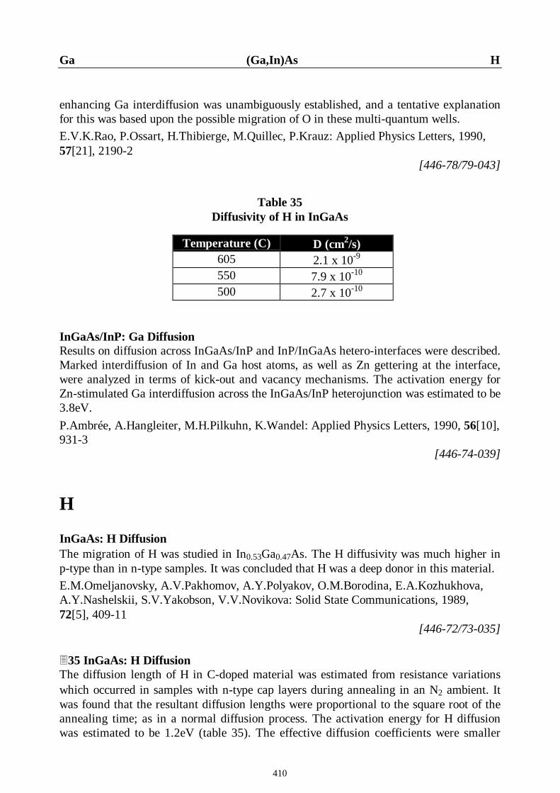
410
Ga (Ga,In)As H
enhancing Ga interdiffusion was unambiguously established, and a tentative explanationfor this was based upon the possible migration of O in these multi-quantum wells.E.V.K.Rao, P.Ossart, H.Thibierge, M.Quillec, P.Krauz: Applied Physics Letters, 1990,57[21], 2190-2
[446-78/79-043]
Table 35Diffusivity of H in InGaAs
Temperature (C) D (cm2/s)605 2.1 x 10⁻⁹
550 7.9 x 10⁻¹⁰
500 2.7 x 10⁻¹⁰
InGaAs/InP: Ga DiffusionResults on diffusion across InGaAs/InP and InP/InGaAs hetero-interfaces were described.Marked interdiffusion of In and Ga host atoms, as well as Zn gettering at the interface,were analyzed in terms of kick-out and vacancy mechanisms. The activation energy forZn-stimulated Ga interdiffusion across the InGaAs/InP heterojunction was estimated to be3.8eV.P.Ambrée, A.Hangleiter, M.H.Pilkuhn, K.Wandel: Applied Physics Letters, 1990, 56[10],931-3
[446-74-039]
H
InGaAs: H DiffusionThe migration of H was studied in In0.53Ga0.47As. The H diffusivity was much higher inp-type than in n-type samples. It was concluded that H was a deep donor in this material.E.M.Omeljanovsky, A.V.Pakhomov, A.Y.Polyakov, O.M.Borodina, E.A.Kozhukhova,A.Y.Nashelskii, S.V.Yakobson, V.V.Novikova: Solid State Communications, 1989,72[5], 409-11
[446-72/73-035]
335 InGaAs: H DiffusionThe diffusion length of H in C-doped material was estimated from resistance variationswhich occurred in samples with n-type cap layers during annealing in an N2 ambient. Itwas found that the resultant diffusion lengths were proportional to the square root of theannealing time; as in a normal diffusion process. The activation energy for H diffusionwas estimated to be 1.2eV (table 35). The effective diffusion coefficients were smaller
411
H (Ga,In)As In
than those in GaAs, thus implying that group-III atoms strongly affected H diffusion in C-doped compound semiconductors.H.Ito: Japanese Journal of Applied Physics, 1996, 35[2-9B], L1155-7
[446-141/142-110]
InGaAs/AlGaAs: H DiffusionThe effects of monatomic H diffusion in quantum wells were studied by usingphotoluminescence and secondary ion mass spectroscopic methods. The multiplequantum well structures were grown by means of molecular beam epitaxy and werehydrogenated with a remote plasma. A significant increase in the 77K photoluminescenceintegrated intensity of bound excitons was observed after hydrogenation. This wasattributed to the passivation of non-radiative recombination centers within the quantumwells. The studies demonstrated that there was an increase in passivation efficiency withincreasing Al concentration in the barriers, and that the hydrogenation was stable totemperatures above 450C. Overall, the results all strongly suggested that the passivatednon-radiative recombination centers were interface defects.S.M.Lord, G.Roos, J.S.Harris, N.M.Johnson: Journal of Applied Physics, 1993, 73[2],740-8
[446-106/107-113]
In
GaInAs/GaAs: In DiffusionThe enhancement of In interdiffusion, due to Zn diffusion, was studied in strained Inx
Ga1-xAs/GaAs single quantum well structures, where x was between 0.20 and 0.24. Thestructures were grown by means of metalorganic vapor base epitaxy, and consisted of a1000 to 2000nm-thick GaAs buffer layer plus an 8 to 10nm GaInAs layer, and a 50 to100nm GaAs cap layer. Shallow Zn in-diffusion was carried out at temperatures ofbetween 585 and 620C, in order to vary the Zn content of the quantum wells. Thesamples were then annealed at temperatures of between 650 and 785C (in AsH3-H2mixtures) in order to determine the enhanced In-Ga interdiffusion coefficient. The resultsfor a typical case could be described by:
D(cm2/s) = 3 x 10⁻⁶ exp[-2.33(eV)/kT]The interdiffusion enhancement was explained in terms of an interstitial migrationprocess.M.T.Furtado, E.A.Sato, M.A.Sacilotti: Superlattices and Microstructures, 1991, 10[2],225-30
[446-88/89-042]
GaInAs/GaAs: In DiffusionA strained single quantum well of GaAs/Ga0.77In0.23Ga/GaAs was grown, via low-pressuremetal-organic vapor phase epitaxy, onto a (100)GaAs substrate at 625C. Samples wereannealed under AsH3/H2 at temperatures ranging from 750 to 900C. Since the quantum

412
In (Ga,In)As In
well thickness of about 8nm was below the critical value for this lattice-mismatchedsystem, it was assumed that the GaInAs layer was commensurate with the GaAs substrate.The low-temperature (2K) photoluminescence of the electron to heavy hole transition inthe quantum well of these samples was analyzed in order to study In/Ga interdiffusion atthe GaInAs/GaAs interfaces. The energies of the photoluminescence peaks shifted tohigher values during annealing. These shifts were quantitatively interpreted in terms ofchanges in the quantum well profile, due to In and Ga interdiffusion. The interdiffusioncoefficient at 850C was deduced to be 3 x 10-17cm2/s; with an activation energy of2.07eV. The values which were obtained for the In/Ga interdiffusion coefficient werelarger than the published values for Al and Ga interdiffusion in AlGaAs/GaAsheterojunctions.F.Iikawa, P.Motisuke, J.A.Brum, M.A.Sacilotti, A.P.Roth, R.A.Masut: Journal of CrystalGrowth, 1988, 93, 336-41
[446-64/65-173]
InGaAs/GaAs/AlGaAs: In DiffusionThe interdiffusion of In and Ga at an InGaAs/GaAs interface was studied. Theinterdiffusion coefficients and activation energies were determined by correlating shifts inphotoluminescence peaks with calculated quantum well transition energies that werebased upon an erf concentration profile. The results indicated that a higher x-value, inInxGa1-xAs single quantum wells, led to a higher interdiffusion coefficient for In under Asover-pressure annealing conditions. Moreover, an increase in the As over-pressureincreased the tendency to interdiffusion, whereas a Ga over-pressure reducedinterdiffusion. The thermal activation energies for x-values of 0.057, 0.1 or 0.15 rangedfrom 3.3 to 2.6eV under an As over-pressure, and from 3 to 2.23eV under a Ga over-pressure.K.Y.Hsieh, Y.L.Hwang, J.H.Lee, R.M.Kolbas: Journal of Electronic Materials, 1990,19[12], 1417-23
[446-84/85-052]
InGaAs/InAlAs: In DiffusionThe distribution of group-III metals at In0.53Ga0.47As/In0.52Al0.48As interfaces, before andafter annealing at 1085K, were measured. Little evidence for Al interdiffusion was found,but the Ga concentration profiles exhibited some broadening after annealing. The almostconstant original In profiles developed strong modulations; with near-discontinuities atthe initial interfaces. This behavior was explained in terms of In diffusion in the chemicalpotential gradient which was established by the disparity in Al and Ga mobilities and bythe requirement for III-V stoichiometry in the alloys.R.J.Baird, T.J.Potter, G.P.Kothiyal, P.K.Bhattacharya: Applied Physics Letters, 1988,52[24], 2055-7
[446-62/63-223]

413
In (Ga,In)As Mn
InGaAs/InAlAs: In DiffusionIt was shown that implantation of O (a basically non-dopant impurity), after adequatehigh-temperature furnace annealing (750C, 1h), led to significant interdiffusion of group-III atoms in molecular beam epitaxially grown In0.53Ga0.47As-In0.52Al0.48As multi-quantum wells. Photoluminescence and Auger electron spectroscopic measurements(coupled with Ar+ ion etching) were used to monitor the disordering of multi-quantumwells which were implanted with O (5 x 10¹³ to 5 x 10¹⁴/cm2) and then annealed by usingeither rapid thermal annealing or long-term furnace annealing. The role which was playedby O in enhancing In interdiffusion was unambiguously established, and a tentativeexplanation for this was based upon the possible migration of O in these multi-quantumwells.E.V.K.Rao, P.Ossart, H.Thibierge, M.Quillec, P.Krauz: Applied Physics Letters, 1990,57[21], 2190-2
[446-78/79-043]
Mg
InGaAs/InP: Mg DiffusionHeterojunctions which were grown by using liquid-phase epitaxy were investigated byusing I-V and Io(T) measurements. It was shown that the injection of electrons across thehetero-interface was described well by a thermionic emission model which involved abarrier height that was strongly affected by p-type dopant diffusion. Heterojunctionbipolar transistors with Schottky collectors were used as tools to measure the injectioncurrent in as-grown p+-In0.53Ga0.47As/n-InP diodes, and the results were compared withthe predictions of the thermionic emission model. In this way, the relative diffusivities ofthe three p-type dopants in InP at 600C were evaluated. The results could be summarizedby:
DBe/DMn ˜ 20, DMg/DBe ˜ 1P.S.Whitney, J.C.Vicek, C.G.Fonstad: Journal of Applied Physics, 1987, 62[5], 1920-4
[446-55/56-028]
Mn
InGaAs/InP: Mn DiffusionHeterojunctions which were grown by using liquid-phase epitaxy were investigated byusing I-V and Io(T) measurements. It was shown that the injection of electrons across thehetero-interface was described well by a thermionic emission model which involved abarrier height that was strongly affected by p-type dopant diffusion. Heterojunctionbipolar transistors with Schottky collectors were used as tools to measure the injectioncurrent in as-grown p+-In0.53Ga0.47As/n-InP diodes, and the results were compared withthe predictions of the thermionic emission model. In this way, the relative diffusivities of
414
Mn (Ga,In)As Si
the three p-type dopants in InP at 600C were evaluated. The results could be summarizedby:
DBe/DMn ˜ 20, DMg/DBe ˜ 1P.S.Whitney, J.C.Vicek, C.G.Fonstad: Journal of Applied Physics, 1987, 62[5], 1920-4
[446-55/56-028]
P
InGaAs/InGaAsP: P DiffusionA photoluminescence study was made of the interdiffusion of P in theIn0.66Ga0.33As/In0.66Ga0.33As0.7P0.3 system at temperatures ranging from 950 to 600C. Itwas shown that the diffusion was Fickian, with no dependence of the diffusion coefficientupon the substrate dopant-type or etch-pit density. In the case of Sn- or S-dopedsubstrates, the diffusion could be described by:
D(cm2/s) = 23 exp[-3.7(eV)/kT]at temperatures greater than 675C. This activation energy was the same as that deducedfor group-III interdiffusion in Ga0.8In0.2As/GaAs. At lower temperatures, diffusivity in thepresent system could be described by:
D(cm2/s) = 5 x 10⁻¹⁰ exp[-1.7(eV)/kT]W.P.Gillin, S.S.Rao, I.V.Bradley, K.P.Homewood, A.D.Smith, A.T.R.Briggs: AppliedPhysics Letters, 1993, 63[6], 797-9
[446-106/107-116]
Si
InGaAs: Si DiffusionThe behavior of implanted Si+ ions was investigated during rapid thermal annealing attemperatures of between 600 and 900C. The apparent activation energy for Si was equalto 0.64eV. Higher activation efficiencies were found for the dopant in InGaAs, ascompared with InAlAs. The Si underwent no migration, even after annealing at 850C.E.Hailemariam, S.J.Pearton, W.S.Hobson, H.S.Luftman, A.P.Perley: Journal of AppliedPhysics, 1992, 71[1], 215-20
[446-86/87-038]
InGaAs/InP: Si DiffusionIt was found that Si-induced mixing produced comparable anion and cation interdiffusion.This was consistent with a di-vacancy mechanism. The mixing depended markedly uponthe Si content and occurred above the diffusion shoulder, where the vacancy and defectpair concentrations were greatly enhanced. The absence of strain-related growth defects in

415
Si (Ga,In)As Zn
the un-strained starting material permitted the formation of a high-quality strained-layersuperlattice by mixing.S.A.Schwarz, P.Mei, T.Venkatesan, R.Bhat, D.M.Hwang, C.L.Schwartz, M.Koza,L.Nazar, B.J.Skromme: Applied Physics Letters, 1988, 53[12], 1051-3
[446-62/63-223]
Ti
InGaAs: Ti DiffusionSamples of n-type In0.53Ga0.47As were implanted with Co and Fe, and p-type samples ofthe same material were implanted with Ti. In the case of high-temperature single-energyCo and Fe implantation, no satellite peaks were observed at locations such as 0.8R, R +dR, or 2R, where R was the projected range and dR was the straggle of the implant.During high-temperature annealing, out-diffusion of the implant was as severe as that forroom-temperature implants. In-diffusion of the implant also occurred, but it was not assevere as the out-diffusion. High-temperature annealing of Ti-implanted material resultedin slight Ti in-diffusion, with minimal redistribution or out-diffusion. In the case of high-temperature implants, the lattice quality of the annealed material was close to that ofvirgin material. Regardless of the ion type, resistivities that were close to the intrinsiclimit were measured in implanted and annealed materials.M.V.Rao, S.M.Gulwadi, S.Mulpuri, D.S.Simons, P.H.Chi, C.Caneau, W.P.Hong,O.W.Holland, H.B.Dietrich: Journal of Electronic Materials, 1992, 21[9], 923-8
[446-93/94-038]
Zn
InGaAs: Zn DiffusionThe diffusion of Zn into In0.57Ga0.43As was studied by using boat diffusion, diffusionfrom As- or P-doped spun-on films, or diffusion from In-doped spun-on films. The depthprofiles were deduced from junction positions. It was found that the p+/p- junctionposition depended upon the diffusion method which was used, but not upon the samplegrowth technique. The p-/n junction position depended upon both factors. Because theamounts of As, Ga and In (or of the respective vacancies) differed, it was possible toidentify diffusion mechanisms. It was proposed that interstitially diffusing Zn wasindependently trapped by 2 immobile vacancy centers. These consisted of Zn on VIn orVGa in the p+ region, and Zn on VAsZnVAs in the p- region.U.König, H.Haspeklo, P.Marschall, M.Kuisl: Journal of Applied Physics, 1989, 65[2],548-52
[446-72/73-035]

416
Zn (Ga,In)As Zn
InGaAs: Zn DiffusionA secondary ion mass spectroscopic study demonstrated that, during the growth of Zn-doped In0.53Ga0.47As layers by atmospheric-pressure organometallic vapor-phase epitaxy,Zn atoms which were trapped on interstitial sites during growth, rather than interstitial Zndefects which were generated by the kick-out mechanism, were probably the main causeof the carrying over of Zn into subsequent layers. The interstitial Zn incorporationseemed to be due to the saturation of In substitution, rather than of Ga substitution. It waspossible that the use of pauses in the growth sequence, both before and after the growthof a Zn-doped layer, could control these effects.S.J.Taylor, B.Beaumont, J.C.Guillaume: Semiconductor Science and Technology, 1993,8[12], 2193-6
[446-115/116-143]
InGaAs: Zn DiffusionSecondary ion mass spectrometry and electrochemical profiling studies were made of thesaturation of Zn doping and diffusion in In0.53Ga0.47As which had been grown onto InP byusing organometallic vapor-phase epitaxy. It was found that the results were consistentwith a so-called kick-out mechanism. It was proposed that the diffusing species wasprobably a neutral Zn interstitial. Accumulation of Zn at the interface with a highly n-doped layer indicated the possible formation of Zn-donor complexes.S.J.Taylor, B.Beaumont, J.C.Guillaume: Semiconductor Science and Technology, 1993,8[5], 643-6
[446-115/116-143]
GaInAs: Zn DiffusionA systematic study of Zn incorporation showed that the surface Zn concentration inmetalorganic vapor phase epitaxial material could be increased from a grown-inmaximum of 2 x 10¹⁹, to 1020/cm3, by diffusion from a spun-on glass source. Thesevalues were found to depend upon the type of p-dopant element which was used in as-grown double heterostructures.D.L.Murrell: Semiconductor Science and Technology, 1990, 5[5], 414-20
[446-74-030]
GaInAs/GaAs: Zn DiffusionThe enhancement of In and Ga interdiffusion, due to Zn diffusion, was studied in strainedInxGa1-xAs/GaAs single quantum well structures, where x was between 0.20 and 0.24. Thestructures were grown by means of metalorganic vapor base epitaxy, and consisted of a1000 to 2000nm-thick GaAs buffer layer plus an 8 to 10nm GaInAs layer, and a 50 to100nm GaAs cap layer. Shallow Zn in-diffusion was carried out at temperatures ofbetween 585 and 620C, in order to vary the Zn content of the quantum wells. The sampleswere then annealed at temperatures of between 650 and 785C (in AsH3-H2 mixtures) in
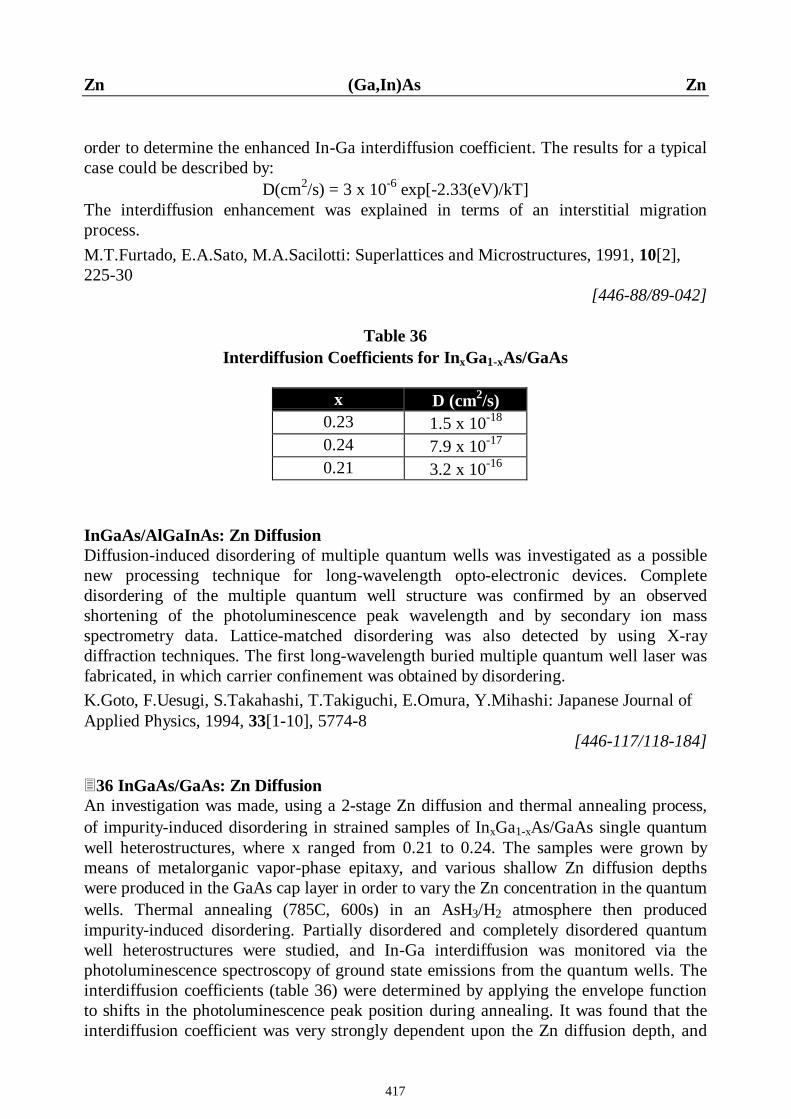
417
Zn (Ga,In)As Zn
order to determine the enhanced In-Ga interdiffusion coefficient. The results for a typicalcase could be described by:
D(cm2/s) = 3 x 10⁻⁶ exp[-2.33(eV)/kT]The interdiffusion enhancement was explained in terms of an interstitial migrationprocess.M.T.Furtado, E.A.Sato, M.A.Sacilotti: Superlattices and Microstructures, 1991, 10[2],225-30
[446-88/89-042]
Table 36Interdiffusion Coefficients for InxGa1-xAs/GaAs
x D (cm2/s)0.23 1.5 x 10⁻¹⁸
0.24 7.9 x 10⁻¹⁷
0.21 3.2 x 10⁻¹⁶
InGaAs/AlGaInAs: Zn DiffusionDiffusion-induced disordering of multiple quantum wells was investigated as a possiblenew processing technique for long-wavelength opto-electronic devices. Completedisordering of the multiple quantum well structure was confirmed by an observedshortening of the photoluminescence peak wavelength and by secondary ion massspectrometry data. Lattice-matched disordering was also detected by using X-raydiffraction techniques. The first long-wavelength buried multiple quantum well laser wasfabricated, in which carrier confinement was obtained by disordering.K.Goto, F.Uesugi, S.Takahashi, T.Takiguchi, E.Omura, Y.Mihashi: Japanese Journal ofApplied Physics, 1994, 33[1-10], 5774-8
[446-117/118-184]
336 InGaAs/GaAs: Zn DiffusionAn investigation was made, using a 2-stage Zn diffusion and thermal annealing process,of impurity-induced disordering in strained samples of InxGa1-xAs/GaAs single quantumwell heterostructures, where x ranged from 0.21 to 0.24. The samples were grown bymeans of metalorganic vapor-phase epitaxy, and various shallow Zn diffusion depthswere produced in the GaAs cap layer in order to vary the Zn concentration in the quantumwells. Thermal annealing (785C, 600s) in an AsH3/H2 atmosphere then producedimpurity-induced disordering. Partially disordered and completely disordered quantumwell heterostructures were studied, and In-Ga interdiffusion was monitored via thephotoluminescence spectroscopy of ground state emissions from the quantum wells. Theinterdiffusion coefficients (table 36) were determined by applying the envelope functionto shifts in the photoluminescence peak position during annealing. It was found that theinterdiffusion coefficient was very strongly dependent upon the Zn diffusion depth, and
418
Zn (Ga,In)As Zn
therefore upon the Zn concentration in the quantum well layer. A model was proposedthat used an interstitial migration process to explain the enhancement of In-Gainterdiffusion by Zn diffusion.M.T.Furtado, M.S.S.Loural, E.A.Sato, M.A.Sacilotti: Semiconductor Science andTechnology, 1992, 7[6], 744-51
[446-99/100-092]
InGaAs/InGaAsP: Zn DiffusionThe stability of the Zn profile in modulation-doped multiple quantum well structures,which had been grown by means of low-pressure metalorganic vapor-phase epitaxy, wasinvestigated by applying secondary ion mass spectrometric and transmission electronmicroscopic techniques to wedge-shaped samples. Although an excellent stability of theZn profile was observed in as-grown samples with modulation doping (3nm, 1018Zn/cm3),the modulation-doped structure faded after the second epitaxial re-growth of a p-type InPlayer (1018Zn/cm3) using either liquid-phase epitaxial or metalorganic vapor-phaseepitaxial techniques. However, the modulation-doping profile was successfully preservedeven after re-growth of the p-type InP layer for 1.5h (in a sample that comprised anundoped InP-clad layer, instead of a p-type InP clad layer, superposed on the modulation-doped multiple quantum well structure layers). The Zn diffusion coefficient in themodulation-doped region was less than 7 x 10-18cm2/s. The maximum Zn concentration,for obtaining a stable modulation-doping structure in the modulation-doped region ofbarrier layers, was found to be 2 x 10¹⁸/cm3. It was proposed that the suppression ofinterstitial Zn atoms, and of subsequently produced interstitial group-III atoms (whichwere generated in the p-type InP clad layer via a kick-out mechanism and diffused intothe multiple quantum well region), was important in preserving the modulation-dopedstructure.N.Otsuka, M.Ishino, Y.Matsui: Journal of Applied Physics, 1996, 80[3], 1405-13
[446-138/139-097]
InGaAs/InP: Zn DiffusionPhotodiodes were fabricated via selective Zn diffusion using a dimethylzinc source. Theresults showed that this method was a useful process for fabricating such devices.M.Wada, M.Seko, K.Sakakibara, Y.Sekiguchi: Japanese Journal of Applied Physics,1990, 29[3], L401-4
[446-76/77-024]
InGaAs/InP: Zn DiffusionA closed-ampoule technique was used to study the simultaneous diffusion of Cd and Zninto material which was lattice-matched to InP. It was found that the Cd atoms, whoseinterstitial diffusion coefficient was small when compared with that of Zn interstitials,penetrated into the crystal as deeply as the Zn atoms. These data agreed with the results of
419
Zn (Ga,In)As Zn
numerical simulations of simultaneous diffusion, in III-V compounds, which were basedupon an interstitial-substitutional diffusion mechanism.U.Wielsch, P.Ambrée, B.Gruska: Semiconductor Science and Technology, 1990, 5[9],923-7
[446-76/77-024]
InGaAs/InP: Zn DiffusionThe diffusion of Zn from spun-on films, and into InP/InGaAs/InP heterostructures, wasstudied. Marked segregation occurred at the InGaAs/InP heterojunctions and increasedthe Zn concentration in InGaAs by about an order of magnitude. Diffusion andsegregation parameters were deduced from the Zn concentration profiles.F.Dildey, M.C.Amann, R.Treichler: Japanese Journal of Applied Physics, 1990, 29[5],810-2
[446-76/77-024]
InGaAs/InP: Zn DiffusionResults on diffusion across InGaAs/InP and InP/InGaAs hetero-interfaces were described.It was found that marked changes in the group-III sub-lattice occurred, near to theinterface, when Zn diffused across the heterojunction from an InGaAs top layer. Thegettering of Zn at the interface was analyzed in terms of kick-out and vacancymechanisms. The activation energy for Zn-stimulated Ga interdiffusion across theInGaAs/InP heterojunction was estimated to be 3.8eV.P.Ambrée, A.Hangleiter, M.H.Pilkuhn, K.Wandel: Applied Physics Letters, 1990, 56[10],931-3
[446-74-039]
InGaAs/InP: Zn DiffusionThe Zn was introduced, using spun-on films, into n-InP/p+-InGaAs/n-InP heterostructureswhich had been grown via metalorganic vapor phase epitaxy (with Mg as a p-dopant).After diffusion, the Mg was completely replaced by Zn and was enriched in the spun-onfilm. In the presence of Mg, the in-diffusion of Zn was strongly enhanced. By varying thedopant level and diffusion conditions, the underlying mechanism was compared with thatwhich operated in Be-doped AlGaAs/GaAs heterostructures.F.Dildey, R.Treichler, M.C.Amann, M.Schier, G.Ebbinghaus: Applied Physics Letters,1989, 55[9], 876-8
[446-70/71-118]
InGaAs/InP: Zn DiffusionIt was found that Zn-induced mixing mainly affected the cation sub-lattice of thesuperlattice and was consistent with a so-called interstitial kick-out mechanism. The Zn-diffused superlattice remained sharply defined. The absence of strain-related growth

420
Zn (Ga,In)As General
defects in the un-strained starting material permitted the formation of a high-qualitystrained-layer superlattice by mixing.S.A.Schwarz, P.Mei, T.Venkatesan, R.Bhat, D.M.Hwang, C.L.Schwartz, M.Koza,L.Nazar, B.J.Skromme: Applied Physics Letters, 1988, 53[12], 1051-3
[446-62/63-223]
InGaAs/InP: Zn DiffusionThe intermixing of multiple quantum well structures by Zn diffusion at 550C wasinvestigated. Secondary ion mass spectroscopy and X-ray analysis revealed that Zndiffusion promoted the intermixing of group-III atoms, but had little effect upon group-Vprofiles. However, the resultant group-III atom profiles were not completely uniform;even after Zn diffusion. The results suggested that a large lattice mismatch suppressed theZn diffusion intermixing process.K.Nakashima, Y.Kawaguchi, Y.Kawamura, Y.Imamura, H.Asahi: Applied PhysicsLetters, 1999, 52[17], 1383-5
[446-62/63-223]
InGaAs/InP: Zn DiffusionA systematic study was made of the effects of Zn doping and diffusion in capped mesaburied heterostructure lasers which had been grown by means of metalorganic chemicalvapor deposition. It involved varying the Zn content (7 x 10¹⁷ to 3.1 x 10¹⁸/cm3) of the p-type InP cladding layer in the base epitaxial structure, while keeping the growthconditions constant during 2 subsequent re-growth steps. Secondary ion massspectrometry was used to make quantitative determinations of the Zn depth profiles,following re-growth, by using test sites on 50mm round wafers which contained theappropriate epitaxial layers. Clear evidence of Zn diffusion was found, such as thepenetration of Zn into the active layer and the presence of inflection points (accumulationand depletion of Zn near to the p-n heterojunction) in the depth profiles. It was observedthat the diffusion of Zn during the third growth step dominated the Zn profile in the basegrowth part of the p-type InP layer, and the final amount of Zn in this region wasindependent of the initial dopant level. Above a Zn threshold level of about 2.2 x10¹⁸/cm3, the Zn diffusion increased significantly and resulted in the presence of 5 x10¹⁸/cm3 or more of Zn in the active layer. The threshold for the onset of diffusion wasfound to be in accord with the substitutional-interstitial diffusion of Zn.V.Swaminathan, C.L.Reynolds, M.Geva: Applied Physics Letters, 1995, 66[20], 2685-7
[446-121/122-079]
General
InGaAs/InGaAsP/InP: DiffusionLaser structures, with InGaAs quantum wells which were about 1.85µ below the surface,were implanted with ions that had energies of up to 8.6MeV. Intermixing of the quantumwells, during rapid thermal annealing, was monitored via changes in the energy, line-

421
General (Ga,In)As Surface
width and intensity of the photoluminescence peaks from the quantum wells. Whendiffusion occurred mainly through InP, the photoluminescence data correlated well withthe calculated total number of vacancies that were created in the sample. This suggestedthat defect diffusion was very efficient in InP.P.J.Poole, S.Charbonneau, G.C.Aers, T.E.Jackman, M.Buchanan, M.Dion,R.D.Goldberg, I.V.Mitchell: Journal of Applied Physics, 1995, 78[4], 2367-71
[446-123/124-177]
InGaAs: DiffusionA theoretical model was proposed for the calculation of the layer thickness of a III-Vternary crystal which was grown by using the source-current controlled method. Thelatter could be used to control the supply of depleted solute elements to a solution duringgrowth. That is, solute elements were continuously supplied to the growth solution from asource material and were transported to a substrate (through the temperature gradient inthe growth solution) via diffusion and electromigration. By using the theoretical model,analytical calculations could be made of the diffusion-limited and electromigration-limited growth of InGaAs in temperature gradient In-Ga-As ternary solutions. Thecalculations indicated that the thickness depended upon growth parameters such as thegrowth temperature, the cooling rates of the substrate and source, the solution length, thetemperature difference between substrate and source, the mobility of the migrating soluteelement, and the electric field in the solution.K.Nakajima: Journal of Crystal Growth, 1989, 98[3], 329-40
[446-72/73-035]
InGaAs/GaAs/AlGaAs: DiffusionLaser structures, with InGaAs quantum wells which were about 1.85µ below the surface,were implanted with ions that had energies of up to 8.6MeV. Intermixing of the quantumwells, during rapid thermal annealing, was monitored via changes in the energy, line-width and intensity of the photoluminescence peaks from the quantum wells. When thedefects had to diffuse mainly through Al0.71Ga0.29As, these quantities were closelyrelated, for short annealing times, to the predicted vacancy generation and ion depositionat the depth of the quantum well before annealing. This suggested that the defectdiffusion length in AlGaAs and/or GaAs was quite low.P.J.Poole, S.Charbonneau, G.C.Aers, T.E.Jackman, M.Buchanan, M.Dion,R.D.Goldberg, I.V.Mitchell: Journal of Applied Physics, 1995, 78[4], 2367-71
[446-123/124-177]
Surface Diffusion
GaInGaAs: Ga Surface DiffusionSurface diffusion during molecular beam epitaxy was studied. Firstly, the mode transitionbetween 2-dimensional nucleation and step flow during molecular beam epitaxial growth
422
Surface (Ga,In)As Interdiffusion
on vicinal surfaces was studied theoretically and experimentally. The basis of the theorywas to assume that the transition occurred when the surface supersaturation on the stepterrace became identical to the critical supersaturation for 2-dimensional nucleation. Thispermitted the diffusion length of Ga to be calculated at the experimentally determinedcritical temperature for the mode transition. It was found that the diffusion lengthincreased, as the temperature decreased, due to an increased residence time. Also, thediffusion length on (111)B was longer than that on (001) when the same formation energyfor 2-dimensional nuclei was assumed for both surfaces. The theory was then used toelucidate the dependence of the InGaAs composition upon the growth temperature, thesubstrate orientation, and the degree of misorientation. The theory gave good agreementwith the experimental data, and it was concluded that surface diffusion was one of themost important processes which controlled molecular beam epitaxial growth and impurityincorporation.T.Nishinaga, T.Shitara, K.Mochizuki, K.I.Cho: Journal of Crystal Growth, 1990, 99, 482-90
[446-76/77-009]
In
GaInAs/GaAs: In Surface DiffusionThe lateral profiles of In in a 1.5µ-thick Ga1-xInxAs layers, where x was approximatelyequal to 0.2, were grown onto GaAs channelled substrates with (411)A side-slopes by theuse of molecular beam epitaxy and were investigated with the use of energy-dispersive X-ray spectroscopy. The observed profiles of the In content suggested that the In atomsmigrated preferentially in the [122] direction on the (411)A plane during molecular beamepitaxial growth. This preferential migration of In atoms was confirmed by comparing theobserved lateral profiles of In in GaInAs layers which had been grown onto GaAschannelled substrates with simulated In profiles that had been calculated by takingaccount of an additional one-way flow of In atoms along [122].T.Kitada, A.Wakejima, N.Tomita, S.Shimomura, A.Adachi, N.Sano, S.Hiyamizu: Journalof Crystal Growth, 1995, 150[1-4], 487-91
[446-127/128-141]
Interdiffusion
GaInAs/AlGaInAs: InterdiffusionInvestigations were made of the interdiffusion behavior and thermal stability of n-dopedand undoped multiple quantum-well structures that were lattice-matched to InP by meansof molecular beam epitaxy. The activation energy for the main interdiffusion process wasdeduced to be 2.5eV for doped structures and 2.9eV for undoped structures. The differinginterdiffusion processes were monitored by using photoluminescence spectroscopy at 8K,after rapid thermal annealing. The effect of doping was studied by comparing the results

423
Interdiffusion (Ga,In)As Interdiffusion
for n-doped and undoped structures. Photoluminescence excitation spectroscopic data for2K confirmed the differing interdiffusion processes.V.Hofsäss, J.Kuhn, H.Schweizer, H.Hillmer, R.Lösch, W.Schlapp: Journal of AppliedPhysics, 1995, 78[5], 3534-6
[446-123/124-172]
GaInAs/AlInAs: InterdiffusionThe interaction of lattice-matched heterostructures, grown by means of molecular beamepitaxy, was studied by using electron microscopy. An appreciable amount ofinterdiffusion was observed at temperatures as low as 700C. The use of X-ray micro-analysis revealed that interdiffusion occurred along a non-linear (non lattice-matched)path.R.E.Mallard, N.J.Long, G.R.Booker, E.G.Scott, M.Hockly, M.Taylor: Journal of AppliedPhysics, 1991, 70[1], 182-92
[446-91/92-018]
Figure 8: Interdiffusivity in InGaAs/GaAs
1.0E-19
1.0E-18
1.0E-17
1.0E-16
1.0E-15
1.0E-14
7 8 9 10 11
table 34table 37table 38table 39table 40table 41table 42
104/T(K)
D (c
m2 /s
)

424
Interdiffusion (Ga,In)As Interdiffusion
GaInAs/GaAs: InterdiffusionThe dependence of impurity-free interdiffusion upon the properties of a dielectric caplayer was studied in pseudomorphic multi-quantum well structures that had been grownby means of molecular beam epitaxy. Electron-beam evaporated SiO2 films, chemicalvapor deposited SiOxNy films, and spun-on SiO2 films were used as cap layers duringrapid thermal annealing at temperatures of between 850 and 950C. Thephotoluminescence at 10K was used to monitor interdiffusion-induced band-gap shifts,and to calculate the corresponding In-Ga interdiffusion coefficients. The latter were foundto increase with cap layer thickness (electron-beam SiO2) up to a limit which wasgoverned by saturation of the out-diffused Ga concentration in the SiO2 caps. Amaximum concentration of between 4 x 10¹⁹ and 7 x 10¹⁹/cm3 in the SiO2 caps was foundby using secondary ion mass spectroscopic profiling. Larger band-edge shifts were alsoobtained when the O content of SiOxNy cap layers was increased, but the differences wereinsufficient to suggest a laterally selective interdiffusion process that was based uponvariations in cap layer composition alone. Much larger differences were obtained byusing various deposition techniques for the cap layers. This indicated that the porosity ofthe cap layer was a much more important factor than was the film composition inobtaining a laterally selective interdiffusion process. In the case of Ga0.8In0.2As/GaAsinterdiffusion, the activation energies and pre-factors were estimated to range from 3.04to 4.74eV and from 5 x 10⁻³ to 2 x 105cm2/s, respectively; depending upon the cap layerdeposition technique and the depth of the multi-quantum well below the sample surface.S.Bürkner, M.Maier, E.C.Larkins, W.Rothemund, E.P.O’Reilly, J.D.Ralston: Journal ofElectronic Materials, 1995, 24[7], 805-12
[446-125/126-131]
337 GaInAs/GaAs: InterdiffusionThe effects of Si and Be, at doping levels of up to 1019/cm3, upon the interdiffusion ofquantum wells after annealing were studied by using photoluminescence techniques (table37). It was found that, for Be concentrations of up to 2.5 x 10¹⁹/cm3, and for Siconcentrations of up to 1018/cm3, no change in the interdiffusion coefficients could bemeasured. At a Si dopant concentration of 6 x 10¹⁸/cm3, there was a dramatic degradationof the material quality after annealing (750C, 15s). This caused the luminescence fromthe well to disappear, while a deep-level luminescence that was related to donor-Gavacancy complexes and As antisite defects appeared. On the basis of these results, it wassuggested that the position of the Fermi level played no role in the intermixing of III-Vheterostructures. It was also concluded that most of the enhanced intermixing which wasobserved in Si-doped GaAs/AlGaAs structures was related to Si relocation at very highdoping levels.W.P.Gillin, I.V.Bradley, L.K.Howard, R.Gwilliam, K.P.Homewood: Journal of AppliedPhysics, 1993, 73[11], 7715-9
[446-106/107-082]

425
Interdiffusion (Ga,In)As Interdiffusion
Table 37Interdiffusion Data for Ga0.8In0.2As/GaAs
Dopant Amount (/cm3) Temperature (C) Coefficient (cm2/s)- - 900 4.70 x 10⁻¹⁷
- - 950 1.96 x 10⁻¹⁶
- - 1000 5.50 x 10⁻¹⁶
- - 1050 1.00 x 10⁻¹⁵
Si 1017 900 3.50 x 10⁻¹⁷
Si 1017 950 1.26 x 10⁻¹⁶
Si 1017 1000 3.90 x 10⁻¹⁶
Si 1017 1050 7.50 x 10⁻¹⁶
Si 1018 900 1.40 x 10⁻¹⁶
Si 1018 950 4.00 x 10⁻¹⁶
Si 1018 1000 1.20 x 10⁻¹⁵
Si 1018 1050 2.80 x 10⁻¹⁵
Be 1017 900 5.40 x 10⁻¹⁷
Be 1017 950 1.50 x 10⁻¹⁶
Be 1017 1000 2.50 x 10⁻¹⁶
Be 1017 1050 1.60 x 10⁻¹⁵
Be 1018 900 1.00 x 10⁻¹⁷
Be 1018 950 1.02 x 10⁻¹⁶
Be 1018 1000 4.20 x 10⁻¹⁶
Be 1018 1050 1.33 x 10⁻¹⁵
Be 2.5 x 10¹⁹ 900 3.70 x 10⁻¹⁷
Be 2.5 x 10¹⁹ 950 1.64 x 10⁻¹⁶
Be 2.5 x 10¹⁹ 1000 5.00 x 10⁻¹⁶
Be 2.5 x 10¹⁹ 1050 2.40 x 10⁻¹⁵
GaInAs/GaAs: InterdiffusionSimple analytical expressions were derived for the approximate estimation of theinterdiffusion coefficient, of partially disordered quantum-well heterostructures, directlyfrom measurements of the photoluminescence phase shift which was associated with layerinterdiffusion. The phase shift was calculated as a function of the interdiffusion length,(Dt)½, in the strained-layer system, Ga0.8In0.2As/GaAs. The calculations were performedwithin the framework of the envelope function approximation and Fick's law. A simplerelationship was derived for the variation in phase shift as a function of the dimensionless

426
Interdiffusion (Ga,In)As Interdiffusion
parameter, (Dt)½/L, where L was the quantum-well thickness. This satisfactorilyaccounted for most of the published interdiffusivity values, to within a factor of 2.M.T.Furtado, M.S.S.Loural: Superlattices and Microstructures, 1993, 14[1], 21-5
[446-113/114-029]
GaInAs/GaAs: InterdiffusionMolecular-beam epitaxially grown highly strained Ga0.65In0.35As/GaAs multiple quantum-well structures were investigated. Interdiffusion was carried out via rapid thermal annealing,at temperatures of between 700 and 950C, by using GaAs proximity caps and electron-beamevaporated SiO2 cap layers, respectively. Reduced photoluminescence line-widths andincreased photoluminescence intensities were observed after diffusion-induced band-gapshifts that ranged from 0.006 to 0.220eV. Microscopic photoluminescence methods wereused to study the onset of strain relaxation due to dislocation generation. Two types of linedefect were found in samples which had been annealed using proximity caps; dependingupon the annealing temperature and the number of quantum wells. These were misfitdislocations with their lines parallel to <110> directions, and <100>-oriented line defects.No dislocations were observed, in samples which had been annealed using a SiO2 cap, overthe entire temperature range which was investigated here. Resonant Raman scatteringmeasurements of the 1LO/2LO phonon intensity ratio were used to make semi-quantitativeassessments of the total defect content; including point defects. It was found that, whereasincreasing point defect densities, and the formation of line defects, were observed inproximity-capped samples as the annealing temperature was increased, no deterioration ofstructural quality due to an increased point defect density was observed in samples whichhad been annealed using a SiO2 cap.S.Bürkner, M.Baeumler, J.Wagner, E.C.Larkins, W.Rothemund, J.D.Ralston: Journal ofApplied Physics, 1996, 79[9], 6818-25
[446-134/135-139]
InGaAs/GaAs/Si: InterdiffusionHeterostructures of the form, InxGa1-xAs(5nm)/GaAs(5nm)/Si, were fabricated viametalorganic chemical vapor deposition and were annealed at 750C. A transmission electronmicroscopic study was made of the heterostructure, with particular attention being paid tointerdiffusion between group-III elements. Plan-view transmission electron microscopyrevealed that the epitaxial InxGa1-xAs /GaAs layer consisted basically of small islandcrystals. The morphology of the islands varied as a function of the In content. When x wasgreater than 0.1, the islands coalesced into larger ones; leaving small regions of so-calledsea. The spacings of 022 moiré fringes varied spatially as a result of variations in In contentin the epilayers. Cross-sectional transmission electron microscopic observations showed thatthere was no sharp heteroboundary between the InxGa1-xAs layer and the GaAs layer. Thecontrast of the 002 dark-field image was sensitive to the In content and revealedinterdiffusion between In and Ga.K.Kamei, K.Fujita, Y.Shiba, H.Katahama, Y.Maehara: Defect and Diffusion Forum,1993, 95-98, 977-82
[446-95/98-977]
427
Interdiffusion (Ga,In)As Interdiffusion
GaInAs/GaInAsP: InterdiffusionElectron microscopy was used to characterize metalorganic chemical vapor depositedmultiple quantum well structures which underwent a so-called blue shift in luminescenceduring thermal processing. The sample exhibited a shift, towards shorter wavelengths, ofmore than 100nm during annealing at 750C. The structural modifications which led to theblue shift included the elimination of atomic ordering in the quaternary barrier layers ofthe material, plus appreciable layer interdiffusion. A method was described by whichquantitative analyses of the layer composition and lattice parameter could be obtained, ata spatial resolution of better than 2nm, by making energy-dispersive X-ray microanalysesin a scanning transmission electron microscope. Such analyses showed that interdiffusionoccurred along a non-linear (non lattice-matched) path, where the group-V diffusivitiesexceeded those of group-III elements. This resulted in the incorporation of excesscoherency strains, of up to 0.5%, in the quantum-well regions.R.E.Mallard, N.J.Long, E.J.Thrush, K.Scarrott, A.G.Norman, G.R.Booker: Journal ofApplied Physics, 1993, 73[9], 4297-304
[446-106/107-091]
InGaAs/GaAs: InterdiffusionThe compositional disordering of superlattices which had been grown by means ofmolecular beam epitaxy, using a low-temperature GaAs cap layer, was studied.Disordering of the superlattice was verified by photoluminescence and double-crystal X-ray rocking curve measurements. The disordering mechanism was found to involve Gavacancy-enhanced interdiffusion, due to the presence of the low-temperature GaAs. Thediffusion and Schrödinger’s equations were solved numerically in order to obtain thecompositional profile and the transition energies in the disordered quantum well,respectively. The simulated energy shifts for samples under various annealing conditionsagreed well with experimental data. The calculated effective diffusivity for In-Gainterdiffusion involved an activation energy of 1.63eV. This was smaller than theactivation energy, of 1.93eV, for intrinsic interdiffusion. The diffusivity for the enhancedIn-Ga interdiffusion, due to the presence of low-temperature GaAs, was some 2 orders ofmagnitude larger than the intrinsic In-Ga diffusivity.J.S.Tsang, C.P.Lee, S.H.Lee, K.L.Tsai, C.M.Tsai, J.C.Fan: Journal of Applied Physics,1996, 79[2], 664-70
[446-131/132-179]
InGaAs/GaAs: InterdiffusionThe effect of strain upon cation interdiffusion in quantum wells was described. It wasfound that Fick’s diffusion equation did not correctly describe interdiffusion in aheterostructure with strained layers. It was suggested that the strain altered the crystaldefect concentration, and that the diffusivity was therefore affected by the strain. Adiffusion equation which included the effects of strain was derived and solvednumerically. Experimental photoluminescence peak shifts, as a function of annealing

428
Interdiffusion (Ga,In)As Interdiffusion
time, were closely fitted by this analysis and useful parameters such as a coefficientwhich described InGaAs/GaAs quantum well interdiffusion were deduced.S.W.Ryu, I.Kim, B.D.Choe, W.G.Jeong: Applied Physics Letters, 1995, 67[10], 1417-9
[446-125/126-141]
Table 38Interdiffusivity in Kr-Implanted InGaAs/GaAs
Temperature (C) D (cm2/s)1050 7.71 x 10⁻¹⁵
1000 3.11 x 10⁻¹⁵
950 5.90 x 10⁻¹⁶
925 3.60 x 10⁻¹⁶
900 1.10 x 10⁻¹⁶
875 9.00 x 10⁻¹⁷
825 1.50 x 10⁻¹⁷
750 8.00 x 10⁻¹⁹
InGaAs/GaAs: InterdiffusionLow-pressure metalorganic vapor phase epitaxially grown strained quantum wellstructures were characterized by using photoluminescence and X-ray diffractiontechniques. It was shown that, beyond the pseudomorphic limit, these structures exhibitedconsiderable Ga/In interdiffusion at the interfaces, and partial strain relaxation in thequantum well layers.A.K.Srivastava, B.M.Arora, S.Banerjee: Journal of Electronic Materials, 1994, 23[2],191-4
[446-113/114-036]
338,39,40,41 InGaAs/GaAs: InterdiffusionPhotoluminescence techniques and repeated annealing were used to determine thediffusion coefficients for intermixing in quantum wells and to study the subsequenteffects of ion implantation upon intermixing. It was shown that, after ion implantation, avery fast interdiffusion process occurred which was independent of the nature of theimplanted ion and was thought to be due to the rapid diffusion of interstitials which werecreated during implantation. Following this rapid process, it was found that neither Ganor Kr ions had any effect upon the subsequent interdiffusion coefficient (tables 38 and39). After As implantation, in addition to the initial damage-related process, an enhancedregion of interdiffusion was observed; with a diffusion coefficient which was an order ofmagnitude greater than that of an non-implanted control wafer (tables 40 and 41). Thisenhancement was suggested to be due to the creation of group-III vacancies by As atomswhich moved into group-V lattice sites. The fast process continued until the structure hadbroadened by about 7.5nm, whereupon the diffusion coefficient returned to the non-
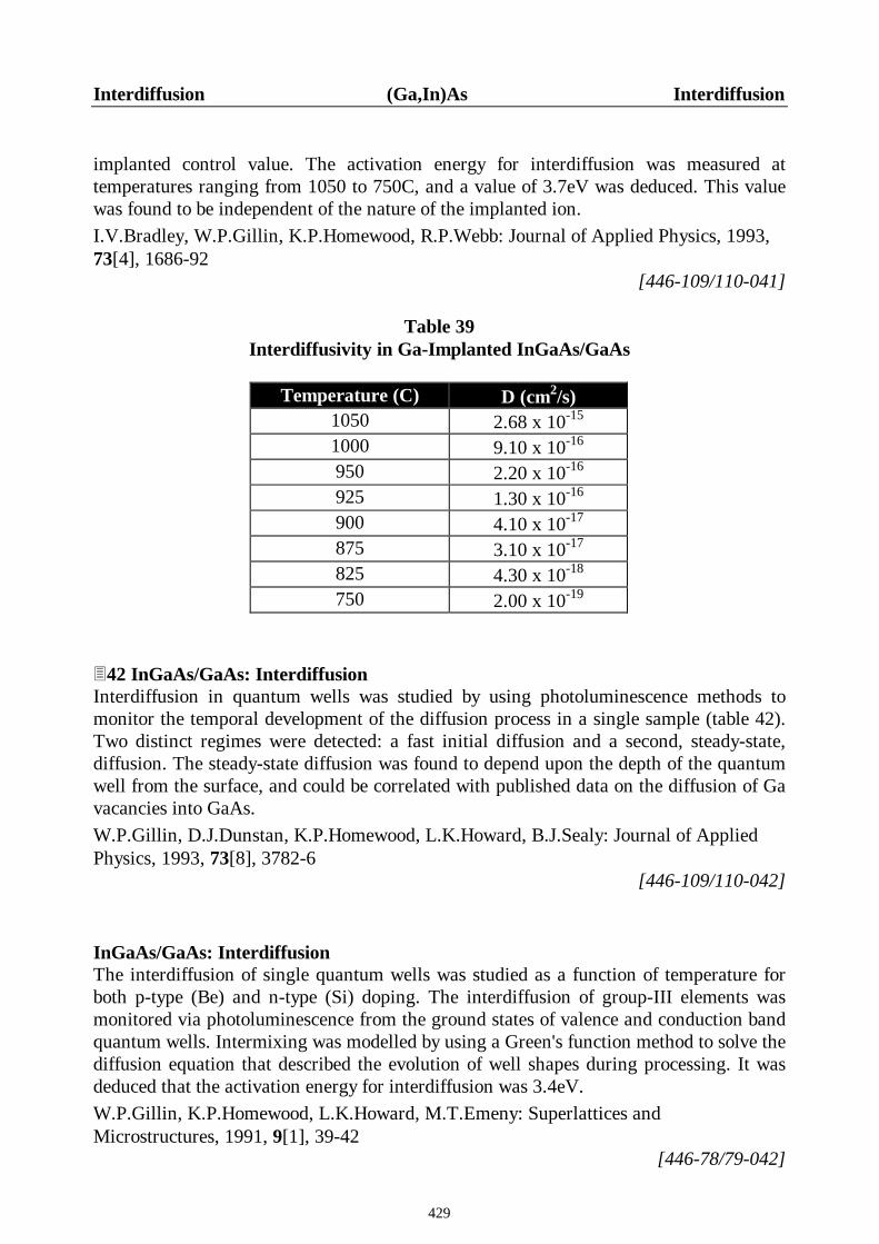
429
Interdiffusion (Ga,In)As Interdiffusion
implanted control value. The activation energy for interdiffusion was measured attemperatures ranging from 1050 to 750C, and a value of 3.7eV was deduced. This valuewas found to be independent of the nature of the implanted ion.I.V.Bradley, W.P.Gillin, K.P.Homewood, R.P.Webb: Journal of Applied Physics, 1993,73[4], 1686-92
[446-109/110-041]
Table 39Interdiffusivity in Ga-Implanted InGaAs/GaAs
Temperature (C) D (cm2/s)1050 2.68 x 10⁻¹⁵
1000 9.10 x 10⁻¹⁶
950 2.20 x 10⁻¹⁶
925 1.30 x 10⁻¹⁶
900 4.10 x 10⁻¹⁷
875 3.10 x 10⁻¹⁷
825 4.30 x 10⁻¹⁸
750 2.00 x 10⁻¹⁹
342 InGaAs/GaAs: InterdiffusionInterdiffusion in quantum wells was studied by using photoluminescence methods tomonitor the temporal development of the diffusion process in a single sample (table 42).Two distinct regimes were detected: a fast initial diffusion and a second, steady-state,diffusion. The steady-state diffusion was found to depend upon the depth of the quantumwell from the surface, and could be correlated with published data on the diffusion of Gavacancies into GaAs.W.P.Gillin, D.J.Dunstan, K.P.Homewood, L.K.Howard, B.J.Sealy: Journal of AppliedPhysics, 1993, 73[8], 3782-6
[446-109/110-042]
InGaAs/GaAs: InterdiffusionThe interdiffusion of single quantum wells was studied as a function of temperature forboth p-type (Be) and n-type (Si) doping. The interdiffusion of group-III elements wasmonitored via photoluminescence from the ground states of valence and conduction bandquantum wells. Intermixing was modelled by using a Green's function method to solve thediffusion equation that described the evolution of well shapes during processing. It wasdeduced that the activation energy for interdiffusion was 3.4eV.W.P.Gillin, K.P.Homewood, L.K.Howard, M.T.Emeny: Superlattices andMicrostructures, 1991, 9[1], 39-42
[446-78/79-042]

430
Interdiffusion (Ga,In)As Interdiffusion
Table 40Interdiffusivity in Non-Implanted InGaAs/GaAs
Temperature (C) D (cm2/s)1050 3.42 x 10⁻¹⁵
1000 8.45 x 10⁻¹⁶
950 1.97 x 10⁻¹⁶
925 1.77 x 10⁻¹⁶
900 4.25 x 10⁻¹⁷
875 2.27 x 10⁻¹⁷
825 1.00 x 10⁻¹⁷
750 2.00 x 10⁻¹⁹
InGaAs/GaAs: InterdiffusionIt was shown that the Si-doping of quantum-well materials to 1019/cm3 promoted a time-and temperature-dependent diffusion process which was related to group-III vacancyformation. The effect of the formation of such vacancies upon subsequent interdiffusionwas modelled and was shown to reproduce variations, in the diffusion coefficient as afunction of depth, without invoking a Fermi-level model. Experiments which wereperformed on layers that were doped to between 1017 and 1018/cm3 did not reveal anenhanced interdiffusion; contrary to the predictions of the Fermi-level model. Otherresults suggested that the reason for this was that interdiffusion in III-V materials was notgoverned by thermal equilibrium vacancy concentrations but rather by the vacancyconcentrations which were grown into the substrate materials. It was demonstrated thatthe position of the Fermi level played no role in III-V intermixing.Z.H.Jafri, W.P.Gillin: Journal of Applied Physics, 1997, 81[5], 2179-84
[446-148/149-182]
InGaAs/InAlAs: InterdiffusionQuantum well structures were grown on InP(Fe) substrates by using metalorganic vaporphase epitaxial techniques. Each sample contained 3 InGaAs wells, which were 2.6, 5.9,or 17.6nm in thickness and were separated by 24nm-thick InAlAs barrier layers. Thesamples were implanted with Si ions to uniform densities which ranged from 1.8 x 10¹⁷ to3.9 x 1019/cm3 over the quantum wells, and were then annealed under various conditions.A photoluminescence peak energy for each well was monitored in order to studyintermixing at the interface. Blue shifts in the photoluminescence peak energy were foundto occur within the first 15s of thermal annealing when the Si dose exceeded a criticalvalue of 2 x 10¹⁸ to 3 x 10¹⁸/cm3. The saturation value of the energy shift was governedmainly by the Si density, but hardly depended upon the annealing temperature and time. Itwas concluded that the defects which were formed by Si ion implantation enhanced the
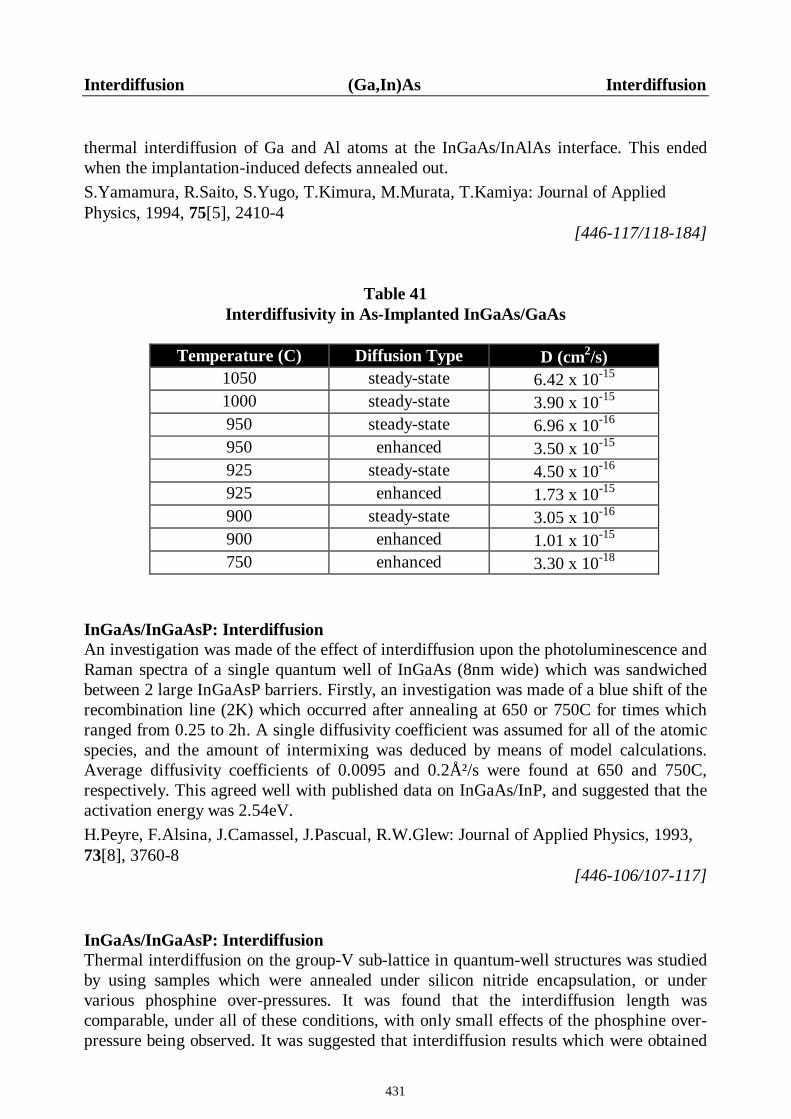
431
Interdiffusion (Ga,In)As Interdiffusion
thermal interdiffusion of Ga and Al atoms at the InGaAs/InAlAs interface. This endedwhen the implantation-induced defects annealed out.S.Yamamura, R.Saito, S.Yugo, T.Kimura, M.Murata, T.Kamiya: Journal of AppliedPhysics, 1994, 75[5], 2410-4
[446-117/118-184]
Table 41Interdiffusivity in As-Implanted InGaAs/GaAs
Temperature (C) Diffusion Type D (cm2/s)1050 steady-state 6.42 x 10⁻¹⁵
1000 steady-state 3.90 x 10⁻¹⁵
950 steady-state 6.96 x 10⁻¹⁶
950 enhanced 3.50 x 10⁻¹⁵
925 steady-state 4.50 x 10⁻¹⁶
925 enhanced 1.73 x 10⁻¹⁵
900 steady-state 3.05 x 10⁻¹⁶
900 enhanced 1.01 x 10⁻¹⁵
750 enhanced 3.30 x 10⁻¹⁸
InGaAs/InGaAsP: InterdiffusionAn investigation was made of the effect of interdiffusion upon the photoluminescence andRaman spectra of a single quantum well of InGaAs (8nm wide) which was sandwichedbetween 2 large InGaAsP barriers. Firstly, an investigation was made of a blue shift of therecombination line (2K) which occurred after annealing at 650 or 750C for times whichranged from 0.25 to 2h. A single diffusivity coefficient was assumed for all of the atomicspecies, and the amount of intermixing was deduced by means of model calculations.Average diffusivity coefficients of 0.0095 and 0.2Ų/s were found at 650 and 750C,respectively. This agreed well with published data on InGaAs/InP, and suggested that theactivation energy was 2.54eV.H.Peyre, F.Alsina, J.Camassel, J.Pascual, R.W.Glew: Journal of Applied Physics, 1993,73[8], 3760-8
[446-106/107-117]
InGaAs/InGaAsP: InterdiffusionThermal interdiffusion on the group-V sub-lattice in quantum-well structures was studiedby using samples which were annealed under silicon nitride encapsulation, or undervarious phosphine over-pressures. It was found that the interdiffusion length wascomparable, under all of these conditions, with only small effects of the phosphine over-pressure being observed. It was suggested that interdiffusion results which were obtained
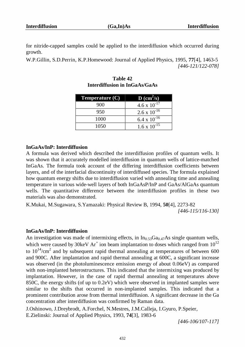
432
Interdiffusion (Ga,In)As Interdiffusion
for nitride-capped samples could be applied to the interdiffusion which occurred duringgrowth.W.P.Gillin, S.D.Perrin, K.P.Homewood: Journal of Applied Physics, 1995, 77[4], 1463-5
[446-121/122-078]
Table 42Interdiffusion in InGaAs/GaAs
Temperature (C) D (cm2/s)900 4.6 x 10⁻¹⁷
950 2.6 x 10⁻¹⁶
1000 6.4 x 10⁻¹⁶
1050 1.6 x 10⁻¹⁵
InGaAs/InP: InterdiffusionA formula was derived which described the interdiffusion profiles of quantum wells. Itwas shown that it accurately modelled interdiffusion in quantum wells of lattice-matchedInGaAs. The formula took account of the differing interdiffusion coefficients betweenlayers, and of the interfacial discontinuity of interdiffused species. The formula explainedhow quantum energy shifts due to interdiffusion varied with annealing time and annealingtemperature in various wide-well layers of both InGaAsP/InP and GaAs/AlGaAs quantumwells. The quantitative difference between the interdiffusion profiles in these twomaterials was also demonstrated.K.Mukai, M.Sugawara, S.Yamazaki: Physical Review B, 1994, 50[4], 2273-82
[446-115/116-130]
InGaAs/InP: InterdiffusionAn investigation was made of intermixing effects, in In0.53Ga0.47As single quantum wells,which were caused by 30keV Ar+ ion beam implantation to doses which ranged from 1012
to 1014/cm2 and by subsequent rapid thermal annealing at temperatures of between 600and 900C. After implantation and rapid thermal annealing at 600C, a significant increasewas observed (in the photoluminescence emission energy of about 0.06eV) as comparedwith non-implanted heterostructures. This indicated that the intermixing was produced byimplantation. However, in the case of rapid thermal annealing at temperatures above850C, the energy shifts (of up to 0.2eV) which were observed in implanted samples weresimilar to the shifts that occurred in non-implanted samples. This indicated that aprominent contribution arose from thermal interdiffusion. A significant decrease in the Gaconcentration after interdiffusion was confirmed by Raman data.J.Oshinowo, J.Dreybrodt, A.Forchel, N.Mestres, J.M.Calleja, I.Gyuro, P.Speier,E.Zielinski: Journal of Applied Physics, 1993, 74[3], 1983-6
[446-106/107-117]

433
Interdiffusion (Ga,In)As Interdiffusion
InGaAs/InP: InterdiffusionThe effects of differing cation and anion interdiffusion rates upon the disordering ofIn0.53Ga0.47As/InP single quantum-wells were investigated by using an erf distribution tomodel the concentration profile after interdiffusion. The early stages of disorderingcaused a spatially dependent strain build-up, which could be compressive or tensile. Thisstrain profile, and the concentration distribution, gave rise to interesting carrierconfinement profiles after disordering. A significantly higher cation interdiffusion rateproduced a red-shift of the ground-state transition energy which, with prolongedinterdiffusion, saturated and then decreased. A significantly higher anion interdiffusionrate caused a blue-shift in the ground-state transition energy, and shifted the light-holeground-state to above the heavy-hole ground-state.W.C.Shiu, J.Micallef, I.Ng, E.H.Li: Japanese Journal of Applied Physics, 1995, 34[1-4A], 1778-83
[446-121/122-078]
InGaAs/InP: InterdiffusionThe interdiffusion of superlattice structures, during annealing at temperatures of between700 and 850C, was studied by means of Raman spectroscopy. The peak intensities andpeak energies of InAs-, GaAs-, and InP-like longitudinal optical phonon modes varied asa function of annealing temperature and time. The depth profiles of group-III and group-Vatoms were estimated quantitatively by monitoring variations in the peak energies of thelongitudinal optical phonon modes, and in the ratios of the mode intensities. This revealedthat the interdiffused superlattice consisted of InGaAsP of uniform composition, and InPbarrier layers with sharp interfaces. It was found that the resultant InGaAsP well wasroughly lattice-matched to InP (to within 0.5%). The diffusion coefficient in the wellregion was larger than that in the barrier region, and the interdiffusion could be describedby:
D(cm2/s) = 8.56 x 10¹⁰ exp[-5.82(eV)/kT]Interdiffusion in this superlattice was governed by diffusion in the InP region.'S.J.Yu, H.Asashi, S.Emura, S.Gonda, K.Nakashima: Journal of Applied Physics, 1991,70[1], 204-8
[446-93/94-039]
InGaAs/InP: InterdiffusionThe thermal stability and interdiffusion of In0.53Ga0.47As/InP surface quantum wells wasinvestigated. Well-defined high-intensity photoluminescence emission spectra wereobtained. After rapid thermal annealing (500 to 900C, 60s), strong emission energy shiftsof up to 0.316eV were detected. By assuming a simple model for ion intermixing, theinterdiffusion coefficient was estimated to be equal to 1.7 x 10⁻¹⁴cm2/s at 900C; with anactivation energy of 1.3eV.J.Oshinowo, A.Forchel, D.Grützmacher, M.Stollenwerk, M.Heuken, K.Heime: AppliedPhysics Letters, 1992, 60[21], 2660-2
[446-88/89-044]
434
Interdiffusion (Ga,In)As Interdiffusion
InGaAs/InP: InterdiffusionQuantum-well structures were studied using magneto-optical transmission spectroscopy.The effects of dopants, overgrowth and annealing were investigated. The blue-shift effect,which was often observed in multiple quantum-well structures that were subjected toheat-treatment, was here attributed to a dominant group-V interdiffusion which could besuppressed by high defect densities in the substrate. The presence of Zn in an overgrownlayer on top of the multiple quantum-well structures caused a counteractive red-shifteffect after long annealing times. This was due to group-III diffusion. On the other hand,in situ Zn or S produced no observable shift in transition energies due to interdiffusion.This was attributed to an enhanced group-III interdiffusion that was induced by Zndiffusion into the multiple quantum-wells. It was concluded that very differentinterdiffusion mechanisms operated in the case of group-III and group-V elements; thussupporting the suggestion of vacancy-related group-V interdiffusion rather than theinterstitialcy mechanism of group-III interdiffusion.S.L.Wong, R.J.Nicholas, R.W.Martin, J.Thompson, A.Wood, A.Moseley, N.Carr: Journalof Applied Physics, 1996, 79[9], 6826-33
[446-134/135-148]

435
(Ga,In)(As,P)
As
InGaAsP/InP: As DiffusionThe effect of diffusion upon quantum-well structures was studied by using secondary ionmass spectrometry, Auger electron spectroscopy, capacitance-voltage measurements,photoluminescence, and X-ray diffraction methods. It was found that the interdiffusion ofAs was negligible.G.J.Van Gurp, W.M.Van de Wijgert, G.M.Fontijn, P.J.A.Thijs: Journal of AppliedPhysics, 1990, 67[6], 2919-26
[446-74-040]
Be
InGaAsP/InP: Be DiffusionA study was made of dopant redistribution between a chemical beam epitaxially grownInGaAsP laser structure, and a metalorganic vapor phase epitaxially over-grown InPlayer. Secondary ion mass spectroscopic data revealed that Zn and Be atoms interdiffuseddeeply into the adjacent InP layers, at a Zn doping level of 1018/cm3. A fraction of the Znatoms went through the chemical beam epitaxial InP, and penetrated the laser structureguide layer. It was found that Zn out-diffusion was appreciably suppressed by reducingthe Be dopant concentration from 1018 to 5 x 10¹⁷/cm3.H.Sugiura, S.Kondo, M.Mitsuhara, S.Matsumoto, M.Itoh: Applied Physics Letters, 1997,70[21], 2846-8
[446-152-0435]
Ga
InGaAsP/InP: Ga DiffusionThe effect of diffusion upon quantum-well structures was studied by using secondary ionmass spectrometry, Auger electron spectroscopy, capacitance-voltage measurements,
436
Ga (Ga,In)(As,P) Si
photoluminescence, and X-ray diffraction methods. It was found that there was markedinterdiffusion of Ga. In a multiple quantum well, Zn diffusion at 500C caused Gaintermixing and the Auger electron spectroscopic profiles became flat. At highertemperatures, an ordering was found such that the Ga concentration was greatest in theoriginal InP layers. This was attributed to the effect of minimization of the free energy;balanced by an increase in the mismatch strain energy. Photoluminescence data revealedthat interdiffusion began at temperatures above 420C.G.J.Van Gurp, W.M.Van de Wijgert, G.M.Fontijn, P.J.A.Thijs: Journal of AppliedPhysics, 1990, 67[6], 2919-26
[446-74-040]
In
InGaAsP/InP: In DiffusionThe effect of diffusion upon quantum-well structures was studied by using secondary ionmass spectrometry, Auger electron spectroscopy, capacitance-voltage measurements,photoluminescence, and X-ray diffraction methods. It was found that there was markedinterdiffusion of In. In a multiple quantum well, Zn diffusion at 500C caused Inintermixing and the Auger electron spectroscopic profiles became flat.G.J.Van Gurp, W.M.Van de Wijgert, G.M.Fontijn, P.J.A.Thijs: Journal of AppliedPhysics, 1990, 67[6], 2919-26
[446-74-040]
P
InGaAsP/InP: P DiffusionThe effect of diffusion upon quantum-well structures was studied by using secondary ionmass spectrometry, Auger electron spectroscopy, capacitance-voltage measurements,photoluminescence, and X-ray diffraction methods. It was found that the interdiffusion ofP was negligible.G.J.Van Gurp, W.M.Van de Wijgert, G.M.Fontijn, P.J.A.Thijs: Journal of AppliedPhysics, 1990, 67[6], 2919-26
[446-74-040]
Si
GaInAsP/GaAs: Si DiffusionThe effect of concurrent Si and Zn diffusion, upon interdiffusion between the cation andanion sub-lattices, was studied in Ga0.95In0.05As0.95P0.05/GaAs heterostructures which hadbeen grown by using liquid-phase epitaxy techniques. The diffusion sources wereequilibrium ternary tie-triangle compositions. The extent of interdiffusion of both group-III and group-V atoms was determined by depth profiling In and P, respectively, using

437
Si (Ga,In)(As,P) Zn
secondary ion mass spectrometry. It was found that Si diffusion enhanced both cation andanion interdiffusion to the same extent. A mono-vacancy mechanism was used to explainthe effect of Si. It was concluded that the impurity diffusion mechanism was a majorfactor which affected the degree of enhancement.K.H.Lee, H.H.Park, D.A.Stevenson: Journal of Applied Physics, 1989, 65[3], 1048-52
[446-72/73-038]
InGaAsP/GaAs: Si DiffusionThe diffusion of SiIII-SiV neutral pairs versus the diffusion of SiIII-VIII complexes in III-Vcrystals was considered with regard to experimental data which revealed the effect of Sidiffusion upon the self-diffusion of column-III and column-V lattice atoms. Secondaryion mass spectroscopy was used to compare the enhanced diffusion of column-III orcolumn-V atoms in various Si-diffused heterostructures which were closely lattice-matched to GaAs. An enhancement of lattice atom self-diffusion, due to impuritydiffusion, was found to occur predominantly on the column-III lattice. The data supportedthe SiIII-VIII diffusion model and indicated that the main native defects whichaccompanied Si diffusion were column-III vacancies. These diffused directly on thecolumn-III sub-lattice.D.G.Deppe, W.E.Plano, J.E.Baker, N.Holonyak, M.J.Ludowise, C.P.Kuo, R.M.Fletcher,T.D.Osentowski, M.G.Craford: Applied Physics Letters, 1988, 53[22], 2211-3
[446-64/65-157]
Zn
InGaAsP: Zn DiffusionThe ampoule diffusion of Zn into liquid-phase epitaxial layers was studied, attemperatures of between 425 and 525C, by means of secondary ion mass spectrometry. Itwas found that the incorporation and diffusion of Zn could be described in terms of theinterstitial-substitutional model. The difference between the acceptor and Znconcentrations was attributed to compensation by Zn interstitial donors or by neutral Zn-vacancy complexes. The diffusion depth was slightly smaller than that in InP and wasmuch larger than that in GaAs. In the case of n-type InGaAsP, the profiles exhibited acut-off which was like that seen in InP.G.J.Van Gurp, D.L.A.Tjaden, G.M.Fontijn, P.R.Boudewijn: Journal of Applied Physics,1988, 64[7], 3468-71
[446-72/73-037]
InGaAsP: Zn DiffusionClosed-ampoule diffusion led to a net acceptor concentration which was lower than theZn concentration. Upon annealing in an atmosphere without Zn, the Zn and net acceptorconcentrations became almost identical. This was attributed to a decreased Znconcentration and an increased net acceptor concentration. The results were quantitativelyexplained by assuming that the Zn was incorporated as both substitutional acceptors and

438
Zn (Ga,In)(As,P) Zn
interstitial donors, and that only the interstitial Zn was driven out by annealing; due to itslarge diffusion coefficient. The profiles which were calculated by using this interstitial-substitutional model could be fitted to experimentally determined profiles by assumingthat the Zn diffused as singly-ionized interstitial donors. The present model alsoexplained published data, on diffusion in n-type InP, in which a profile cut-off was foundat a depth where the acceptor concentration equalled the background donor concentration.G.J.Van Gurp, T.Van Dongen, G.M.Fontijn, J.M.Jacobs, D.L.A.Tjaden: Journal ofApplied Physics, 1989, 65[2], 553-60
[446-72/73-037]
InGaAsP: Zn DiffusionShallow diffusion was improved by using a new spun-on source which was based uponZn-doped alumina. In this case, the thermal expansion coefficients of the diffusion sourceand the semiconductor were better matched than when using Zn-doped silica films. Aswell as excellent mechanical stability of the spun-on films over a wide temperature range,the effect of mechanical stresses upon the diffusion process was effectively reduced.M.C.Amann, G.Franz: Journal of Applied Physics, 1987, 62[4], 1541-3
[446-55/56-029]
GaInAsP/GaAs: Zn DiffusionThe effect of concurrent Zn diffusion upon interdiffusion in an Ga0.94In0.06As0.95P0.05-GaAs heterostructure, grown by means of liquid phase epitaxy, was investigated.Diffusion annealing (700C, 25h) was performed by using an equilibrium ternary diffusionsource, and In and P profiles were measured by using secondary ion mass spectrometry. Itwas found that Zn diffusion selectively enhanced cation (In-Ga) interdiffusion. In the caseof concurrent Zn diffusion, the interdiffusion coefficient for the In-Ga components wasabout 5 x 10-14cm2/s; as compared with about 6 x 10-16cm2/s for anions (As-P). A kick-outmechanism was suggested to explain the results.H.H.Park, K.H.Lee, D.A.Stevenson: Applied Physics Letters, 1988, 53[23], 2299-301
[446-64/65-174]
GaInAsP/GaAs: Zn DiffusionThe effect of concurrent Si and Zn diffusion, upon interdiffusion between the cation andanion sub-lattices, was studied in Ga0.95In0.05As0.95P0.05/GaAs heterostructures which hadbeen grown by using liquid-phase epitaxy techniques. The diffusion sources wereequilibrium ternary tie-triangle compositions. The extent of interdiffusion of both group-III and group-V atoms was determined by depth profiling In and P, respectively, usingsecondary ion mass spectrometry. It was found that Zn diffusion selectively enhancedcation (In, Ga) interdiffusion. A kick-out mechanism was used to explain the selectiveenhancement of cation interdiffusion by Zn. It was concluded that the impurity diffusionmechanism was a major factor which affected the degree of enhancement.K.H.Lee, H.H.Park, D.A.Stevenson: Journal of Applied Physics, 1989, 65[3], 1048-52
[446-72/73-038]

439
Zn (Ga,In)(As,P) Zn
GaInAsP/InP: Zn DiffusionIt was shown that Zn diffusion into a GaxIn1-xAsyP1-y-InP quantum well structure andsuperlattice, with a thickness of 10nm, completely disordered the quantum well and thesuperlattice layers. It was found that the photoluminescence wavelength of the quantumwell and the superlattice had increased after Zn diffusion. This was attributed to In-Gainterdiffusion at the interface, due to an interchange process between interstitials andsubstitutional Zn atoms.M.Razeghi, O.Acher, F.Launay: Semiconductor Science and Technology, 1987, 2[12],793-6
[446-61-077]
InGaAsP/InP: Zn DiffusionThe effect of Zn diffusion upon quantum-well structures was studied by using secondaryion mass spectrometry, Auger electron spectroscopy, capacitance-voltage measurements,photoluminescence, and X-ray diffraction methods. The structures were stable toannealing, in the absence of Zn. In a multiple quantum well, Zn diffusion at 500C causedIn and Ga intermixing and the Auger electron spectroscopic profiles became flat.Photoluminescence data revealed that interdiffusion began at temperatures above 420C.The diffusion of Zn changed the lattice parameter values of InGaAsP and InP so that theaverage value decreased.G.J.Van Gurp, W.M.Van de Wijgert, G.M.Fontijn, P.J.A.Thijs: Journal of AppliedPhysics, 1990, 67[6], 2919-26
[446-74-040]
InGaAsP/InP: Zn DiffusionThe effect of concurrent Zn diffusion upon interdiffusion in a In0.72Ga0.28As0.61P0.39/InPheterostructure was investigated by using Auger electron spectroscopy and secondary ionmass spectrometry. The measured profiles showed that Zn diffusion (600C, 1 to 4h)mainly enhanced cation (In, Ga) interdiffusion. This could not be explained in terms ofthe Zn-vacancy complex model. Results which were obtained under conditions of group-V element over-pressure suggested that cation interstitials could control both the rate ofZn diffusion and the mixing of group-III sub-lattices in the InP-based alloy system.H.H.Park, B.K.Kang, E.S.Nam, Y.T.Lee, J.H.Kim, O.Kwon: Applied Physics Letters,1989, 55[17], 1768-70
[446-72/73-029]
InGaAsP/InP: Zn DiffusionThe degradation of lattice-matched In0.72Ga0.28As0.61P0.39/InP hetero-interfaces during Zndiffusion was investigated by using high-resolution transmission electron microscopy andAuger electron spectroscopy. Diffusion-induced intermixing of In and Ga across theGaInAsP/InP interface produced tensile stresses in the Ga-mixed InP side andcompressive stresses in the In-mixed GaInAsP side. The effects of localized interfacialstresses upon the nucleation of misfit dislocations and upon their strain accommodation

440
Zn (Ga,In)(As,P) Zn
behavior were clearly revealed throughout the intermixed region, and reached severalthousand Å on both sides of the interface. The interfacial strain was relaxed by thegeneration of paired dislocations, with anti-parallel Burgers vectors, which arose from theintermixed GaInAsP/GaInP interface. The dislocation morphologies revealed strikingcontrasts across the intermixed interface; involving stacking faults in the tensile layer andperfect dislocation tangles in the compressive layer. The dislocation lines wereconcentrated at the GaInAsP/GaInP interface and along misfit boundaries in the frontalareas of the intermixed region. A model was proposed, in order to explain the strainrelaxation behavior in the intermixed region, which invoked an homogeneous nucleationmechanism and splitting of the paired dislocations from the intermixed interface.H.H.Park, K.H.Lee, J.K.Lee, Y.T.Lee, E.H.Lee, J.Y.Lee, S.K.Hong, O.Kwon: Journal ofApplied Physics, 1992, 72[9], 4063-72
[446-106/107-118]
InGaAsP/InP: Zn DiffusionAn open-tube Zn diffusion method that involved the use of solid Zn3P2 or InP wasdeveloped, and was used to fabricate heterojunction devices. The diffusion profiles weredetermined by means of secondary ion mass spectrometry. It was found that the diffusiondepth was proportional to the square root of the diffusion time, and that a sharp change inthe Zn concentration was observed at the diffusion front. The activation energies wereequal to 1.2eV for undoped InP, 1.7eV for Sn-doped InP, and 1.1eV for InGaAs.T.Ohishi, K.Ohtsuka, Y.Abe, H.Sugimoto, T.Matsui: Japanese Journal of AppliedPhysics, 1990, 29[2], L213-6
[446-76/77-024]
InGaAsP/InP: Zn DiffusionThe diffusion of Zn into heterostructures, from spun-on polymer films which containedno Si-organic compounds, was investigated. It was shown that the initial non-equilibriumstage of diffusion, and the defect relaxation process, determined the final profile of the Zndistribution; as well as its anomalies. The results demonstrated the important role whichwas played by the kick-out mechanism in the formation of a sharp diffusion profile slopeas well as in Zn gettering at a hetero-interface.B.J.Ber, L.A.Busygina, A.T.Gorelenok, A.V.Kamanin, A.V.Merkulov, I.A.Mokina,N.M.Shmidt, I.J.Yakimenko, T.A.Yurre: Materials Science Forum, 1994, 143-147, 1415-20
[446-113/114-037]
InGaAsP/InP: Zn DiffusionA study was made of dopant redistribution between a chemical beam epitaxially grownInGaAsP laser structure, and a metalorganic vapor phase epitaxially over-grown InPlayer. Secondary ion mass spectroscopic data revealed that Zn and Be atoms interdiffuseddeeply into the adjacent InP layers, at a Zn doping level of 1018/cm3. A fraction of the Znatoms went through the chemical beam epitaxial InP, and penetrated the laser structure

441
Zn (Ga,In)(As,P) Interdiffusion
guide layer. It was found that Zn out-diffusion was appreciably suppressed by reducingthe Be dopant concentration from 1018 to 5 x 10¹⁷/cm3.H.Sugiura, S.Kondo, M.Mitsuhara, S.Matsumoto, M.Itoh: Applied Physics Letters, 1997,70[21], 2846-8
[446-152-0441]
Interdiffusion
InGaAsP/InGaAsP: InterdiffusionThe interdiffusion behavior of In1-xGaxAs1-yPy/In1-x'Gax'As1-y'Py' multiple quantum-wellheterostructures, with various built-in strains and layer thicknesses, was investigated bymonitoring their photoluminescence. All of the samples which were annealed at 850Cconsistently exhibited a blue-shift of the heavy hole exciton line as a result ofinterdiffusion across the hetero-interfaces. Data on a nearly strain-compensated structure,with a constant P/As ratio and In-rich wells, showed that the blue-shift of the excitonicline was the result of group-III atom interdiffusion alone, as in the GaAs/GaAlAs system.The In-Ga interdiffusion could be described by a coefficient of about 4.72 x 10⁻¹⁶cm2/s.In the case of lattice-matched and compressively strained structures, simultaneousinterdiffusion on the group-III and group-V sub-lattices yielded an effective interdiffusioncoefficient which ranged from 3.83 x 10⁻¹⁶ to 5.51 x 10⁻¹⁶cm2/s.A.Hamoudi, A.Ougazzaden, P.Krauz, K.Rao, M.Juhel, H.Thibierge: Japanese Journal ofApplied Physics, 1995, 34[1-1], 36-41
[446-119/120-215]
InGaAsP/InGaAsP: InterdiffusionBy using quaternary/quaternary multiple quantum wells, with constant P/As ratios and In-rich wells, it was shown that it was possible to produce a blue-shift of the heavy holeexciton line by interdiffusing only group-III atoms. The use of this type of structure,which was particularly suitable for group-III diffusion studies, yielded a value (for the In-Ga interdiffusion coefficient) of about 4.72 x 10⁻¹⁶cm2/s at 850C.A.Hamoudi, A.Ougazzaden, P.Krauz, E.V.K.Rao, M.Juhel, H.Thibierge: Applied PhysicsLetters, 1995, 66[6], 718-20
[446-121/122-078]

442
(Ga,In)P
Zn
InGaP: Zn DiffusionThe migration of Zn was studied by using angle-lapping and stain-etching techniques. Itwas found that the Zn diffusion depth was proportional to the square root of the diffusiontime, and depended upon the composition of In1-xGaxP. That is, the effective diffusioncoefficient at a given diffusion temperature decreased according to:
D(cm2/s) = 3.935 x 10⁻⁸ exp[-6.84x]while the activation energy increased according to:
Q(eV) = 1.28 + 2.38xThis was attributed to a decreasing contribution from interstitial diffusion with increasingGa content.S.T.Kim, D.C.Moon: Japanese Journal of Applied Physics, 1990, 29[4], 627-9
[446-76/77-025]
InGaP: Zn DiffusionThe diffusion of Zn was studied, using photoluminescence techniques, in liquid-phaseepitaxial In0.5Ga0.5P layers which had been grown onto semi-insulating GaAs substrates.The photoluminescence exhibited a characteristic emission peak at 1.934eV afterdiffusion. It was found that this peak behaved like donor-acceptor pair recombination andwas associated with the interstitial Zn donor to substitutional Zn acceptor band transition.The calculated activation energy of the substitutional acceptor was 0.047eV.I.T.Yoon, B.S.Jeong, H.L.Park: Thin Solid Films, 1997, 300[1-2], 284-8
[446-157/159-442]
GaInP/GaAs: Zn DiffusionHeterojunction Zn-doped bipolar transistors were prepared by means of metal-organicchemical vapor deposition. The characteristics of heterojunction bipolar transistors withan undoped spacer layer and an n-type GaAs set-back layer (heterostructure-emitter)

443
Zn (Ga,In)P|(Ga,In)Sb Interdiffusion
between base and emitter were investigated. The results showed that base dopant out-diffusion was effectively prevented in heterostructure-emitter bipolar transistors.Y.F.Yang, C.C.Hsu, E.S.Yang: Semiconductor Science and Technology, 1995, 10[3],339-43
[446-121/122-069]
(Ga,In)Sb
Interdiffusion
GaInSb/InAs: InterdiffusionStrained superlattices which exhibited a high degree of structural perfection were grownonto GaSb substrates. The superlattices exhibited ideal defect-free structures. Cross-sectional micrographs revealed that the layers were highly planar, regular and coherentlystrained with respect to the substrate. No crystalline defects were observed by usingtransmission electron microscopy, in spite of the existence of a lattice mismatch of almost2%. The planarity of the layers was confirmed by the observation of Pendellösung fringesin high-resolution X-ray diffraction patterns, while the observation of numerous sharpsatellite peaks indicated that essentially no interdiffusion occurred within thesuperlattices.R.H.Miles, D.H.Chow, W.J.Hamilton: Journal of Applied Physics, 1992, 71[1], 211-4
[446-86/87-033]

444
GaN
D
GaN: D DiffusionThe out-diffusion of H was studied, using 2H plasma-treated (250 or 400C, 0.5h) or 2H+-implanted samples, during annealing at temperatures ranging from 300 to 900C.Secondary ion mass spectrometry was used to measure the resultant distributions. In thecase of plasma-treated samples, 2 populations of 2H were found. At concentrations thatwere greater than 1020/cm3, there was a near-surface (less than 0.3µ) region that wasprobably due to the formation of platelet defects. At concentrations of about 1018/cm3, aplateau region was present which extended throughout the film thickness of about 1µ.This was attributed to the pairing of 2H with point defects. The D in the former regionbegan to out-diffuse at 300C. In the latter region, out-diffusion did not begin until thetemperature exceeded 800C. In implanted samples, 2H redistribution occurred in the samemanner as the bulk population in plasma-treated material. The thermal stability of the Dprofiles in the nitride was much higher than that in GaAs and similar compounds.R.G.Wilson, S.J.Pearton, C.R.Abernathy, J.M.Zavada: Journal of Vacuum Science andTechnology A, 1995, 13[3], 719-23
[446-140-029]
H
GaN: H DiffusionAn investigation was made of interactions between H and dopant impurities, in thismaterial, by using first-principles calculations. The results revealed a fundamentaldifference in the behaviors of H in p-type and n-type samples. In particular, it wasexplained why the H concentrations in n-type material were low, and why H had abeneficial effect upon acceptor incorporation in p-type material. Overall, the conclusionssupported the potential use of H as a means of improving the doping of wide-bandgapsemiconductors, although the approach was not generally applicable. In order to be able toexploit H passivation as a method for enhancing doping, the H had to be the predominantcompensating defect. That is, its formation energy had to be lower than that of all native
445
H GaN Surface
defects, and be comparable to the formation energy of the dopant impurity. Also, theactivation energy which was required to dissociate the H-impurity complex, and toremove or neutralize H, had to be lower than the activation energies for native defectformation and lower than the diffusion barrier of the impurity. Finally, the dissociated Hatom had to be highly mobile.J.Neugebauer, C.G.Van de Walle: Applied Physics Letters, 1996, 68[13], 1829-31
[446-134/135-263]
GaN: H DiffusionA study was made, of the electronic structure, energetics, and migration of H and H-complexes, on the basis of first-principles total-energy calculations. The latter revealed anumber of features which were very different to those which were exhibited by H in moretraditional semiconductors such as Si or GaAs. These included a very large negative-Ueffect (of about 2.4eV), an instability of the bond-center site, high energies of Hmolecules, and an unusual geometry of the Mg-H complex. All of these features wereshown to be a result of the particular properties of the present material, such as itsstrongly ionic nature and the high strength of the Ga-N bond. A simple model wasproposed, for the negative-U behavior, which was expected to be valid for H in anysemiconductor.J.Neugebauer, C.G.Van de Walle: Physical Review Letters, 1995, 75[24], 4452-5
[446-127/128-227]
Surface Diffusion
GaN/GaAs: Ga Surface DiffusionMetalorganic vapor phase epitaxial growth of cubic GaN on patterned GaAs(100)substrates which had (111)A or (111)B facets was studied. It was found that the growthfeatures depended strongly upon the configuration of the pattern. It was deduced thatthese features arose from an orientation-dependent growth rate, which varied in the order:(111)B > (100) > (111)A, together with Ga adatom diffusion on the surface. By takingadvantage of the growth on patterned substrates, the diffusion length of Ga adatoms onthe GaAs(100) surface was estimated to be typically equal to several microns.M.Nagahara, S.Miyoshi, H.Yaguchi, K.Onabe, Y.Shiraki, R.Ito: Journal of CrystalGrowth, 1994, 145[1-4], 197-202
[446-119/120-306]
- miscellaneous
GaN: Surface DiffusionThe growth kinetics of GaN/(00?1)sapphire hetero-epitaxial films were studied, atsubstrate temperatures ranging from 560 to 640C, by using reflection high-energyelectron diffraction specular reflection intensity monitoring techniques. An alternating-element exposure growth method was used in which Ga and N atoms were supplied

446
Surface GaN|GaP Ga
separately (rather than simultaneously as usual) to the substrate, with the insertion of atime delay between successive Ga-flux and N-flux exposures. A time-dependent recoveryof the reflection high-energy electron diffraction specular reflection intensity, during thetime delay, was associated with Ga-N surface molecule migration on Ga-terminatedsurfaces. The activation energy for this migration process was deduced to be 1.45eV.H.Liu, J.G.Kim, M.H.Ludwig, R.M.Park: Applied Physics Letters, 1997, 71[3], 347-9
[446-152-0446]
GaPFeGaP: Fe DiffusionThe structural properties of samples which had been implanted with 150 or 400keV Fe orTi, to doses of between 1012 and 1015/cm2, were studied. The depth distributions of theimplants were compared before and after annealing with, or without, a Si3N4 cap.Rutherford back-scattering, X-ray double-crystal diffractometry, and secondary ion massspectroscopy results indicated that Fe was markedly redistributed in all of the materialsduring annealing. On the other hand, Ti did not redistribute at all. The driving force forthe redistribution of Fe was thought to be not classical diffusion, but reaction withimplantation-induced defects and stoichiometric imbalances. The defect chemistry of as-implanted arsenides was found to be fundamentally different to that of as-implantedphosphides since, in the latter case, the mass ratio of the constituents was much greaterand the specific energy for amorphization was much lower.H.Ullrich, A.Knecht, D.Bimberg, H.Kräutle, W.Schlaak: Journal of Applied Physics,1992, 72[8], 3514-21
[446-106/107-034]
Ga
GaP: Ga DiffusionThe self-diffusion of Ga was measured directly in isotopically controlled heterostructures.Secondary ion mass spectroscopy was used to monitor the intermixing of 69Ga and 71Ga

447
Ga GaP General
between isotopically pure GaP epilayers which had been grown, by molecular beamepitaxy, onto GaP substrates. It was found that Ga self-diffusivity in undoped GaP couldbe described by:
D (cm2/s) = 2.0 exp[-4.5(eV)/kT]at temperatures of between 1000 and 1190C, under P-rich condition. The entropy of self-diffusion was estimated to be about 4k.L.Wang, J.A.Wolk, L.Hsu, E.E.Haller, J.W.Erickson, M.Cardona, T.Ruf, J.P.Silveira,F.Briones: Applied Physics Letters, 1997, 70[14], 1831-3
[446-150/151-144]
HGaP: H DiffusionThe H passivation effect of Zn was studied by monitoring donor-acceptor pairluminescence bands. The existence of a critical pair-separation distance was detected,within which neutralization by H was almost entirely suppressed by the presence of anearby donor. This phenomenon was reflected by a relative enhancement of theintensities of the discrete pair lines, as compared to that of the remote pair band in S-Znpair emission. Further evidence was provided by the fact that the intensity reduction inthe O-Zn band was much smaller than that predicted by calculations which assumed arandom neutralization of Zn acceptors. It was suggested that the suppression was due tothe Coulomb potential of a nearby donor atom, and was consistent with the concept thatthe principal diffusing form of H was positively charged.Y.Mochizuki, M.Mizuta: Materials Science Forum, 1992, 83-87, 575-80
[446-99/100-085]
TiGaP: Ti DiffusionThe structural properties of samples which had been implanted with 150 or 400keV Ti, todoses of between 1012 and 1015/cm2, were studied. The depth distributions of the implantswere compared before and after annealing with, or without, a Si3N4 cap. Rutherford back-scattering, X-ray double-crystal diffractometry, and secondary ion mass spectroscopyresults indicated that the Ti did not redistribute at all.H.Ullrich, A.Knecht, D.Bimberg, H.Kräutle, W.Schlaak: Journal of Applied Physics,1992, 72[8], 3514-21
[446-106/107-034]
General
GaP/InP: DiffusionA theoretical study was made of the defect characteristics of a strained-layer superlattice.On the basis of the calculated charge states, some closely-bound interstitial-antisite pairs

448
General GaP Interdiffusion
were found to form at a distance of one bond length in a stable GaP/InP (1 x 1) structure.The defect-related states that were localized in the energy gap suggested that theformation mechanism of the EL2 complex in the GaAs system was inapplicable toGaP/InP multilayer structures. A slow self-diffusion process was proposed for bothgroup-III and group-V atoms in this superlattice. Kick-out reactions were suggested to befavored at higher dopant concentrations.E.G.Wang: Physica Status Solidi B, 1992, 174[2], 367-74
[446-106/107-096]
Surface Diffusion
GaP: Surface DiffusionA scanning tunnelling microscope tip-induced migration of di-vacancies was observed onthe (110) surface of n-doped material. Such motion occurred only for a negative polarityof the tunnelling voltage, and was directed along the [110] direction; regardless of thescanning orientation. It was therefore purely non-thermal. It was suggested that a field-induced reduction of the barrier to migration initiated the motion. A quantitative analysisof the migration indicated the existence of long-lived excited states. This was consistentwith charged trap states in doped semiconductors.P.Ebert, M.G.Lagally, K.Urban: Physical Review Letters, 1993, 70[10], 1437-40
[446-106/107-093]
Interdiffusion
GaP/InP: InterdiffusionThe interdiffusion of lateral composition-modulated (GaP)2/(InP)2 short-periodsuperlattices was studied. Lateral compositional modulation was obtained by using thestrain-induced lateral layer ordering process. A blue-shift of the inter-band transition wasobserved, by means of photoluminescence spectroscopy, in cap-less and SiO2-encapsulated annealed (800C, 5.5h) short-period superlattices. The intensity andwavelength of Si3N4-encapsulated annealed short-period superlattices were only slightlyperturbed. Transmission electron microscopy showed that capless-annealed (800C, 5.5h)short-period superlattices retained their lateral composition modulation. However, the(00½) satellite reflections disappeared. After long (48h) annealing, the inter-bandtransition corresponded to that of an In0.50Ga0.50P alloy. This suggested that the lateralcomposition modulation disappeared. The observed lateral interdiffusion coefficientexceeded the vertical one by a factor of about 30; thus suggesting that short-periodsuperlattice interdiffusion was enhanced by native point defects.J.I.Malin, A.C.Chen, J.E.Bonkowski, J.E.Baker, K.Y.Cheng, K.C.Hsieh: Journal ofApplied Physics, 1996, 80[2], 1233-5
[446-136/137-120]

449
GaSb
H
GaSb: H DiffusionThe use of spreading resistance and capacitance-voltage methods showed that atomic Hpassivated shallow acceptors and donors in this material. Deep-level passivation by Halso occurred, as revealed by deep-level transient spectroscopic measurements ofSchottky diode structures. Effective H diffusion coefficients were deduced for both n+-type and p+-type samples. In the former case, the diffusion was thermally activated andcould be described by:
D(cm2/s) = 3.4 x 10⁻⁵ exp[-0.55(eV)/kT]at temperatures of between 100 and 250C. In the latter case, the diffusivity could bedescribed by:
D(cm2/s) = 1.5 x 10⁻⁶ exp[-0.45(eV)/kT]Reactivation of passivated shallow and deep levels occurred at temperatures of between250 and 300C.A.Y.Polyakov, S.J.Pearton, R.G.Wilson, P.Rai-Choudhury, R.J.Hillard, X.J.Bao,M.Stam, A.G.Milnes, T.E.Schlesinger, J.Lopata: Applied Physics Letters, 1992, 60[11],1318-20
[446-86/87-036]
Sb
GaSb: Sb DiffusionRecovery in crystals which had been implanted with Ga ions, and then subjected to rapidthermal annealing or furnace annealing, was studied by using Raman scatteringtechniques. The intensity of the LO phonon mode decreased with increasing ionimplantation fluence. It was found that the threshold fluence for the amorphization of Ga-implanted GaSb was 5 x 10¹³/cm2. This value was much lower than that for InP(1014/cm2). In the case of furnace annealing, the recovery processes in Ga-implantedmaterial were very different above and below a fluence of 5 x 10¹⁴/cm2. No recovery wasobserved at this critical fluence. At lower fluences, the LO mode intensity increased with

450
Sb GaSb Zn
increasing annealing temperatures and times of up to 400C and of up to 0.25h. However,the damage recovery was very poor when compared with that of GaAs, InP, or GaP. Inthe case of Si3N4-capped rapid thermal annealing, recovery was observed even for afluence of 5 x 10¹⁴/cm2. New modes were observed, at about 114 and 150/cm, inimplanted and annealed samples. These 2 modes were related to the Eg and Alg modes ofSb-Sb bond vibrations, respectively, and were attributed to the out-diffusion of Sb atoms.It was found that furnace annealing enhanced Sb out-diffusion, and that the capped rapidthermal annealing process was superior to the furnace annealing process for the healing ofdamaged layers. These anomalous behaviors were thought to be closely related to theweak bond-strength of Sb-containing materials. The degree of recovery, as a function ofannealing temperature, annealing time, and fluence was also investigated.S.G.Kim, H.Asahi, M.Seta, J.Takizawa, S.Emura, R.K.Soni, S.Gonda, H.Tanoue: Journalof Applied Physics, 1993, 74[1], 579-85
[446-106/107-096]
Te
GaSb: Te DiffusionThe diffusion of Te into undoped p-type material was carried out, and the samples werestudied using cathodoluminescence and photoluminescence techniques. The luminescencecenters in Te-diffused samples were identified and were compared with those in Te-doped bulk material. Essential differences in the radiative levels, between diffused andas-grown doped samples, were observed. Evidence of the presence of self-compensatingacceptor complexes was found in the case of diffused samples. At short and mediumdiffusion times, a compensating acceptor complex, VGaGaSbTeSb, was observed. At longdiffusion times, the predominant acceptor center was suggested to be the antisite defect,GaSb, or a related complex.P.S.Dutta, B.Méndez, J.Piqueras, E.Dieguez, H.L.Bhat: Journal of Applied Physics,1996, 80[2], 1112-5
[446-136/137-120]
Zn
GaSb: Zn DiffusionIt was recalled that Zn diffusion was usually performed in an evacuated quartz ampoule,with one source for the dopant and with a second antimonide source being used toprovide an over-pressure over the GaSb during diffusion. Strict control of the systempartial pressure was required in order to produce reproducible diffusion and damage-freesurfaces. An alternative technique was open-tube diffusion from doped spun-on films.Such dopant emulsions had been successfully applied to some III/V semiconductors. Thepresent work was the first report of the reproducible diffusion of Zn into GaSb from aspun-on diffusion source in an open-tube system. A Zn/SiO2 film was used as the

451
Zn GaSb Zn
diffusion source at temperatures of 630 or 680C. The concentration in the semiconductorcould fall below the substrate dopant level due to the depletion effects of the source.C.Heinz: Journal of the Electrochemical Society, 1988, 135[1], 250-2
[446-61-078]
GaSb: Zn DiffusionThe diffusion of Zn into Te-doped samples was studied as a function of time, temperatureand Sb over-pressure. The overall Zn profiles, as well as carrier concentration profiles,were determined. The results indicated an inverse dependence of the diffusivity upon theSb over-pressure, and reflected the operation of an interstitial-substitutional vacancymechanism. At high Zn concentrations, the profiles indicated the existence of anadditional component which was associated with a non-electrically active Zn species thathad a small, but highly temperature-dependent, diffusion coefficient.G.J.Conibeer, A.F.W.Willoughby, C.M.Hardingham, V.K.M.Sharma: Optical Materials,1996, 6[1-2], 21-5
[446-141/142-104]
GaSb: Zn DiffusionThe diffusion of Zn into Te-doped samples was studied as a function of time,temperature, and Sb over-pressure. The overall Zn profiles, as well as carrierconcentration profiles, were measured. The results indicated the operation of asubstitutional-interstitial vacancy (Frank-Turnbull) or kick-out (Gosele-Morehead)mechanism; although there was insufficient evidence to decide between them. There wasalso an inverse dependence of the diffusivity upon the Sb over-pressure. This wasexplained in terms of a Zn diffusion that was superposed on Ga vacancy diffusion. It wasnoted that Te doping appeared to have little effect upon diffusion, due to its low levelwhen compared to that of Zn. Moreover, at high Zn concentrations, the profiles indicatedthe presence of an additional component that was associated with a non-electrically activeZn species which had a small strongly temperature-dependent diffusion coefficient.G.J.Conibeer, A.F.W.Willoughby, C.M.Hardingham, V.K.M.Sharma: Journal ofElectronic Materials, 1996, 25[7], 1108-12
[446-141/142-105]
GaSb: Zn DiffusionSpin-on diffusion of Zn into samples in an open tube-furnace was investigated by using aZn-doped silica film as a diffusion source. Theoretical calculations were carried out whichassumed the silica film to be an exhaustible source. Diffusion treatments were performedat 630 or 680C, using undiluted or diluted Zn-containing silica films. It was found that thejunction depth exhibited a linear dependence upon the square root of the diffusion time forundiluted films with no source depletion, whereas results which were obtained by diffusionfrom diluted films clearly reflected depletion effects in an exhaustible diffusion

452
Zn GaSb General
source. The method was also applicable to Ga0.935Al0.065Sb, due to its very small Alcontent.C.Heinz: Solid-State Electronics, 1993, 36[12], 1685-8
[446-115/116-134]
GaSb: Zn DiffusionA closed-ampoule technique was used to introduce Zn into Te-doped material. Annealingwas carried out for various times; with or without an Sb over-pressure. The total Znprofiles were measured by using secondary ion mass spectrometry, and carrier profileswere deduced from incremental sheet resistance data. It was found that the diffusivityvaried, with Zn concentration, from 6.3 x 10⁻¹²cm2/s for a concentration of 3 x 10²⁰/cm3
at 500C.G.J.Conibeer, A.F.W.Willoughby, C.M.Hardingham, V.K.M.Sharma: Materials ScienceForum, 1994, 143-147, 1427-32
[446-113/114-031]
GaSb: Zn DiffusionThe diffusion of Zn in n-type material, at temperatures ranging from 450 to 540C, wasstudied. The diffusion was carried out in a closed system, using a Zn-Ga source. Thediffusion profiles were measured by using secondary ion mass spectrometry. On the basisof the diffusion profiles, concentration-dependent diffusion coefficients were calculatedby using Boltzmann-Matano analyses. These data were qualitatively interpreted in termsof an interstitial-substitutional diffusion model which had originally been proposed for Zndiffusion in GaAs.V.S.Sundaram, P.E.Gruenbaum: Journal of Applied Physics, 1993, 73[8], 3787-9
[446-109/110-036]
General
GaSb: DiffusionAn extensive review was presented of advances in the use of GaSb-based systems. Itdetailed all aspects: from bulk crystal growth or epitaxy, post-growth processing to devicedesign. Some current areas of research and development were critically assessed, andtheir significance with respect to the understanding of basic physical phenomena andpractical applicability was addressed. These areas included the role played by defects andimpurities in affecting the structural and other properties of the material, and thetechniques which were used for surface- and bulk-defect passivation. It was concludedthat current knowledge concerning this material was sufficient to explain its basicproperties and permit its further application. Among the topics which were listed were:defects and impurities, extended defects, native defects, isotopic effects, self- andimpurity diffusion, ion bombardment-induced defects, surface and bulk defect

453
General GaSb|InAs H
passivation, H-plasma passivation, and the passivation of amorphous hydrogenatedmaterial.P.S.Dutta, H.L.Bhat, V.Kumar: Journal of Applied Physics, 1997, 81[9], 5821-70
[446-150/151-145]
InAsFeInAs: Fe DiffusionThe structural properties of samples which had been implanted with 150 or 400keV Fe orTi, to doses of between 1012 and 1015/cm2, were studied. The depth distributions of theimplants were compared before and after annealing with, or without, a Si3N4 cap.Rutherford back-scattering, X-ray double-crystal diffractometry, and secondary ion massspectroscopy results indicated that Fe was markedly redistributed in all of the materialsduring annealing. On the other hand, Ti did not redistribute at all. The driving force forthe redistribution of Fe was thought to be not classical diffusion, but reaction withimplantation-induced defects and stoichiometric imbalances. The defect chemistry of as-implanted arsenides was found to be fundamentally different to that of as-implantedphosphides since, in the latter case, the mass ratio of the constituents was much greaterand the specific energy for amorphization was much lower.H.Ullrich, A.Knecht, D.Bimberg, H.Kräutle, W.Schlaak: Journal of Applied Physics,1992, 72[8], 3514-21
[446-106/107-034]
H
InAs: H DiffusionAccidentally doped InAs layers were grown, by molecular beam epitaxy, onto semi-insulating GaAs substrates, and were exposed to H plasma. It was found that the
454
H InAs Zn
diffusivity of H in these layers was high. Hydrogenation led to an order of magnitudeincrease in the free carrier density. At the same time, defect-related peaks disappearedfrom the near-bandedge luminescence spectrum. On the other hand, the properties of bulkInAs or those of InAs-on-InAs layers were not altered by exposure to the H plasma. Amodel which was based upon the passivation, by H, of electronic states which wereinduced by dislocations in InAs-on-GaAs layers was proposed in order to explain theseeffects.B.Theys, S.Kalem, A.Lusson, J.Chevallier, C.Grattepain, M.Stutzmann: MaterialsScience Forum, 1992, 83-87, 629-34
[446-99/100-090]
InAs/GaAs: H DiffusionAtomic H was introduced, into molecular beam epitaxial InAs layers on GaAs substrates,from a plasma source. It was found that the H diffused very rapidly into the material. Itspresence modified the electronic transport properties, the near-bandedge luminescencespectra, and the far-infrared reflectivity. The free-carrier density had increased by anorder of magnitude after hydrogenation. These effects could be removed by thermalannealing.B.Theys, A.Lusson, J.Chevallier, C.Grattepain, S.Kalem, M.Stutzmann: Journal ofApplied Physics, 1991, 70[3], 1461-6
[446-91/92-023]
Ti
InAs: Ti DiffusionThe structural properties of samples which had been implanted with 150 or 400keV Ti, todoses of between 1012 and 1015/cm2, were studied. The depth distributions of the implantswere compared before and after annealing with, or without, a Si3N4 cap. Rutherford back-scattering, X-ray double-crystal diffractometry, and secondary ion mass spectroscopyresults indicated that the Ti did not redistribute at all.H.Ullrich, A.Knecht, D.Bimberg, H.Kräutle, W.Schlaak: Journal of Applied Physics,1992, 72[8], 3514-21
[446-106/107-034]
Zn
InAs: Zn DiffusionElemental Zn was diffused into (100)-oriented samples by using the closed-tube method.The diffusion temperatures ranged from 350 to 500C. It was found that the results couldbe described by:
D(cm2/s) = 0.00016 exp[-1.07(eV)/kT]
455
Zn InAs Surface
H.Khald, H.Mani, A.Joullie: Journal of Applied Physics, 1988, 64[9], 4768-70[446-72/73-034]
Surface Diffusion
In
InAs: In Surface DiffusionThe inter-surface diffusion of In adatoms between a (111)A and a (001) surface on anInAs (111)A-(001) non-planar substrate was investigated for the first time by usingmicroprobe reflection high-energy electron diffraction techniques. It was found that thesurface diffusion of In adatoms depended strongly upon the growth temperature and theAs pressure, but was independent of the In flux. It was also observed that the migrationdirection of the In lateral flux between the (111)A and (001) InAs surfaces changed;depending upon the growth conditions.X.Q.Shen, T.Nishinaga: Journal of Crystal Growth, 1995, 146[1-4], 374-8
[446-127/128-148]
- miscellaneous
InAs: Surface DiffusionThe sensitivity, of the 2- to 3-dimensional growth transition of InAs self-assembledislands, to the InAs coverage was used to demonstrate the growth of self-aligned InAsislands on etched GaAs ridges by molecular beam epitaxy. The differing migrationbehavior of In adatoms upon the various crystal planes of etched ridges was used tomodulate spatially the supply of In adatoms. The ridges were oriented along the [011] and[011] directions on (100) substrates with grating spacings of 0.28, 1 or 5µ. Atomic forcemicroscopy revealed that the InAs islands were self-aligned along the ridges and weretypically 40nm in diameter and 12nm in height. In samples with [011]-oriented ridges, theislands were located on the side-walls. On the other hand, in the case of [011]-orientedridges, the islands were on the (100) planes on, and at the foot of, the mesa. On sampleswith a grating pitch of 0.28µ, all of the islands were located either on the side-walls or atthe bottom of the so-called V-groove: for both grating orientations.D.S.L.Mui, D.Leonard, L.A.Coldren, P.M.Petroff: Applied Physics Letters, 1995, 66[13],1620-2
[446-121/122-074]
InAs: Surface DiffusionThe surface diffusion of group-III atom incorporation during molecular beam epitaxialgrowth was considered. Firstly, the diffusion length for incorporation on the (001) topsurface, with (111)A or (411)A side surfaces on V grooves, was studied. It was shownthat the diffusion length took the same value for both cases and was inversely
456
Surface InAs Interdiffusion
proportional to the As pressure. The same relationship was also found for the diffusion ofIn in InAs during molecular beam epitaxy. However, the diffusion length of Ga on (111)Bexhibited an inverse parabolic dependence of the As pressure. It was suggested that, onthe (001) surface, two As4 molecules met to furnish active As atoms for growth. On theother hand, the behavior of the As4 molecule on the (111)B surface remained unclear. Theratio of the surface diffusion coefficients on (111)B and (001) was calculated. It wasfound that the ratio took a value of about 140. Using this ratio, the incorporation lifetimeson (111)B and (001) surfaces were calculated as functions of the As pressure. It wasfound that the curves of incorporation lifetime intersected at the As pressure where flowinversion occurred.T.Nishinaga, X.Q.Shen, D.Kishimoto: Journal of Crystal Growth, 1996, 163[1], 60-6
[446-138/139-078]
Interdiffusion
InAs/GaAs: InterdiffusionThe existence of interdiffusion, between self-assembled InAs quantum dots and a GaAssubstrate, was investigated by using Rutherford back-scattering techniques. These werealso useful for determining the value of the average InAs layer thickness. As a result, dataon the diffusion of Ga atoms into the dot were obtained.T.Haga, M.Kataoka, N.Matsumura, S.Muto, Y.Nakata, N.Yokoyama: Japanese Journal ofApplied Physics, 1997, 36[2-8B], L1113-5
[446-157/159-456]
InAs/InP: InterdiffusionThe intermixing of ultra-thin strained quantum-well structures, during annealing attemperatures of 730 to 830C, was investigated by means of photoluminescencemeasurements. Upon analyzing the results, using a microscopic model, the interdiffusionprocess was found to be characterized by an activation energy of about 3.8eV. Theinterdiffusion coefficient was close to 7 x 10⁻⁷cm2/s at 830C.J.M.Sallese, S.Taylor, H.J.Bühlmann, J.F.Carlin, A.Rudra, R.Houdré, M.Ilegems:Applied Physics Letters, 1994, 65[3], 341-3
[446-125/126-140]

457
In(As,P)InterdiffusionInAsP/InP: InterdiffusionEvidence was presented for the occurrence of anomalously high strain-dependentinterdiffusion in InAsP layers which had been grown onto InP(001) substrates by meansof organometallic vapor phase epitaxy at 620C. In particular, there were clear indicationsof the existence of a critical strain. If the strain was equal to about 1.9% or more, markedP-As mixing occurred. At smaller strains, the degree of mixing was greatly reduced. Theincidence of interdiffusion was also highly sensitive to the temperature. A set of sampleswhich was prepared at 580C exhibited an approximately 2-fold decrease in P-As mixing,as compared with samples that were prepared at 620C.D.J.Tweet, H.Matsuhata, P.Fons, H.Oyanagi, H.Kamei: Applied Physics Letters, 1997,70[25], 3410-2
[446-152-0457]
In(As,Sb)ZnInAsSb: Zn DiffusionElemental Zn was diffused into (100)-oriented samples of InAs1-xSbx, where x rangedfrom 0.10 to 0.12, by using the closed-tube method. The diffusion temperatures rangedfrom 350 to 500C. It was found that the results could be described by:
D(cm2/s) = 0.00016 exp[-1.07(eV)/kT]H.Khald, H.Mani, A.Joullie: Journal of Applied Physics, 1988, 64[9], 4768-70
[446-72/73-034]
458
InNDInN: D DiffusionThe out-diffusion of H was studied, using 2H plasma-treated (250 or 400C, 0.5h) or 2H+-implanted samples, during annealing at temperatures ranging from 300 to 900C.Secondary ion mass spectrometry was used to measure the resultant distributions. Atconcentrations that were greater than 1020/cm3, there was a near-surface (less than 0.3µ)region that was probably due to the formation of platelet defects. At concentrations ofabout 1018/cm3, a plateau region was present which extended throughout the filmthickness of about 1µ. This was attributed to the pairing of 2H with point defects. Inimplanted samples, 2H redistribution occurred in the same manner as the bulk populationin plasma-treated material. The thermal stability of the D profiles in the nitride was muchhigher than that in GaAs and similar compounds.R.G.Wilson, S.J.Pearton, C.R.Abernathy, J.M.Zavada: Journal of Vacuum Science andTechnology A, 1995, 13[3], 719-23
[446-140-029]
InP
Au
InP: Au DiffusionMigration of Au at temperatures ranging from 400 to 700C was studied by usingsecondary ion mass spectrometry. Low values were found for the diffusion coefficient;

459
Au InP Cd
which was equal to 2 x 10-12cm2/s at 550C. By using deep-level transient spectroscopy,Au was found to behave as a shallow donor with a level that was situated at 0.55eV fromthe conduction band. It was concluded that Au thermal migration from contacts was notthe mechanism which was responsible for device degradation.V.Parguel, P.N.Favennec, M.Gauneau, Y.Rihet, R.Chaplain, H.L'Haridon, C.Vaudry:Journal of Applied Physics, 1987, 62[3], 824-7
[446-55/56-029]
Be
InP: Be DiffusionImplantation (1.5 x 10¹⁴/cm2) of 30keV Be into (x11)A-oriented semi-insulating InPsubstrates (where x took values of up to 4) was carried out. For comparison, (110)- and(100)-oriented substrates were also implanted. The in-diffusion of Be in (311)A-orientedsubstrates was lower than that in (100) material.M.V.Rao, H.B.Dietrich, P.B.Klein, A.Fathimulla, D.S.Simons, P.H.Chi: Journal ofApplied Physics, 1994, 75[12], 7774-8
[446-117/118-166]
InP: Be DiffusionModels were presented for the distribution profiles of Be in ion-doped layers afterimplantation and annealing. The possibility of predicting the mean free path of Be in III-V compounds was considered. The effect of defect-impurity interactions upon Bediffusion was also examined. It was found that a flux of impurities towards the surfaceoccurred which was not diffusive in nature.G.I.Koltsov, V.V.Makarov, S.J.Yurchuk: Fizika i Tekhnika Poluprovodnikov, 1996,30[10], 1907-16 (Semiconductors, 1996, 30[10], 996-1000)
[446-148/149-171]
Cd
InP: Cd DiffusionThe so-called leaky tube method was used to diffuse elemental Cd into InP at 500C, andthe junction depths were determined after various times. It was found that the diffusioncoefficient was concentration-dependent, and ranged from about 10-14 to 10-10cm2/s.C.B.Wheeler, R.J.Roedel, R.W.Nelson, S.N.Schauer, P.Williams: Journal of AppliedPhysics, 1990, 68[3], 969-72
[446-86/87-042]
InP: Cd DiffusionThe Cd was diffused into InP by using Cd3P2 plus P or Cd3P2 plus Cd3As2 as diffusionsources. Two diffusion fronts were observed. The diffusion characteristics of Cd3P2 plus P

460
Cd InP D
sources were explained in terms of the interstitial-substitutional model or the vacancycomplex model. The charge state of the diffusing interstitial Cd atom was a singly ionizeddonor. The chemical species of P which reacted with InP was P2, and gaseous Cdoriginated from solid-phase CdP2. In the case of Cd3P2 plus Cd3As2 diffusion sources, theeffective diffusion coefficient and the surface acceptor concentration decreased withincreasing weight fraction of Cd3As2. The relative depth of the deeper diffusion frontincreased when the supply of vacancies was suppressed.K.I.Ohtsuka, T.Matsui, H.Ogata: Japanese Journal of Applied Physics, 1988, 27[2], 253-9
[446-60-009]InP: Cd DiffusionPhase diagrams between Cd and III-V compounds were investigated in order to developnew acceptor diffusion sources. On the basis of thermodynamic data and experimentalstudies of the Cd-Ga-As and Cd-In-P phase diagrams, it was found that Zn3Cd3B2 andZnCdB2 were suitable acceptor sources in that they did not erode the semiconductorsurface.S.F.Marenkin, O.N.Pashkova, V.N.Ravich, I.Z.Babievskaya, N.N.Kazarina,J.A.Poroikov: Izvestiya Akademii Nauk SSSR - Neorganicheskie Materialy, 1990, 26[9],1814-8. (Inorganic Materials, 1991, 26[9], 1552-5)
[446-84/85-054]
CuInP: Cu DiffusionA study of Cu diffusion in both p-type and n type samples showed that this materialexhibited a transition to semi-insulating behavior at relatively low Cu diffusiontemperatures. It was found that all, or most, of the Cu precipitates formed a Cu-Incompound, that both originally n-type and p-type material became semi-insulating, andthat there was a negligibly low concentration of deep-level defects. It was observed thatthere was an abnormal reduction in both electron and hole mobilities, which resulted fromthe introduction of Cu, and that there were isolated pockets of highly conductive materialin otherwise semi-insulating material. It was concluded that all of these experimentalobservations could be best explained by the buried Schottky barrier model instead ofcompensation by deep levels.R.P.Leon, M.Kaminska, K.M.Yu, Z.Liliental-Weber, E.R.Weber: Materials ScienceForum, 1992, 83-87, 723-8
[446-99/100-093]
DInP: D DiffusionData on the effusion of D from various samples were presented. It was shown that theeffusion was limited by surface phenomena, and that decomposition of the sample surfaceplayed a major role.B.Theys, J.Chevallier, M.Miloche, B.Rose: Materials Science Forum, 1994, 143-147,945-50
[446-113/114-037]

461
D InP Fe
InP: D DiffusionThe problem of hydrogenating this material without causing surface degradation wassolved by exposing the surface to a plasma via a thin SiNx(H) cap. This layer waspermeable at the hydrogenation pressure of 250C, but was impermeable to P or PH3. Itwas found that shallow acceptors were heavily passivated, whereas shallow donors wereonly weakly affected. The presence of acceptors impeded D in-diffusion. Thus, Ddiffusion under the same conditions occurred to a depth of 0.018mm in p-type (2 x 10¹⁶
Zn/cm3) material, but to a depth of 0.035mm in n-type (S, Sn) material.W.C.Dautremont-Smith, J.Lopata, S.J.Pearton, L.A.Koszi, M.Stavola, V.Swaminathan:Journal of Applied Physics, 1989, 66[5], 1993-6
[446-74-040]
Fe
InP: Fe DiffusionThe diffusion of Fe was found to occur via the kick-out mechanism. A published Fediffusion profile in InP was simulated by using the complete set of 3 partial differentialequations for the kick-out mechanism. A value for the contribution which In self-interstitials made to the self-diffusion coefficient of InP was deduced and was found to bemuch smaller than was suggested by the known self-diffusion coefficients which hadbeen determined from In tracer diffusion measurements.H.Zimmermann, U.Gösele, T.Y.Tan: Applied Physics Letters, 1993, 62[1], 75-7
[446-106/107-120]
InP: Fe DiffusionThe doping and diffusion characteristics of Fe in semi-insulating layers were assessed byusing secondary ion mass spectrometry. Fairly flat Fe depth profiles, and a linear dopingcurve, were obtained at concentrations of up to 1017/cm3. Accumulation of Fe at thesubstrate/layer interface was found in some samples; thus revealing a gettering effect ofthe substrate. Very little, and probably negligible, diffusion was observed on alternatelyFe-doped and undoped structures; even after high-temperature heat treatment (providedthat the Fe content was about 1016/cm3 or less).D.Franke, P.Harde, P.Wolfram, N.Grote: Journal of Crystal Growth, 1990, 100[3], 309-12
[446-76/77-026]
InP: Fe DiffusionThe structural properties of samples which had been implanted with 150 or 400keV Fe orTi, to doses of between 1012 and 1015/cm2, were studied. The depth distributions of theimplants were compared before and after annealing with, or without, a Si3N4 cap.Rutherford back-scattering, X-ray double-crystal diffractometry, and secondary ion massspectroscopy results indicated that Fe was markedly redistributed in all of the materialsduring annealing. On the other hand, Ti did not redistribute at all. The driving force for

462
Fe InP Fe
the redistribution of Fe was thought to be not classical diffusion, but reaction withimplantation-induced defects and stoichiometric imbalances. The defect chemistry of as-implanted arsenides was found to be fundamentally different to that of as-implantedphosphides since, in the latter case, the mass ratio of the constituents was much greaterand the specific energy for amorphization was much lower.H.Ullrich, A.Knecht, D.Bimberg, H.Kräutle, W.Schlaak: Journal of Applied Physics,1992, 72[8], 3514-21
[446-106/107-034]
InP: Fe DiffusionIt was pointed out that high-resistivity material could be grown by metalorganic vaporphase epitaxy, using ferrocene as a dopant source. Adjacent Zn-doped layers removed theresistivity of Fe-doped material. The presence of Zn markedly enhanced the out-diffusionof Fe from Fe-doped layers, and into Zn-doped material. It was suggested that interstitialZn took over the lattice sites of substitutional Fe. The Fe then became interstitial andmobile.E.W.A.Young, G.M.Fontijn: Applied Physics Letters, 1990, 56[2], 146-7
[446-74-040]
InP: Fe DiffusionA new technique, which involved a Zn3P2 diffusion source and rapid thermal annealing,was studied. A p+-type layer could be obtained only at temperatures of between 500 and550C by using a 15s diffusion time. The diffusivity was calculated and was comparedwith the results of furnace annealing. The present diffusivity was deduced to be equal to2.6 x 10-12cm2/s. In order to form a shallow layer, it was necessary to avoid anytreatments which might redistribute Fe or dopants. Annealing (850C, 15s) beforediffusion shifted the carrier profile from 300 to 600nm in depth. The second diffusionfront extended to 0.0024mm in a semi-insulating substrate. Diffusion treatments whichwere performed on samples without pre-annealing resulted in 2 diffusion fronts. A0.0028mm-deep second diffusion front was found when the treatment was applied to apre-annealed epi-wafer. The diffusivity under these conditions was deduced to be equal to1.4 x 10-11cm2/s.K.W.Wang, S.M.Parker, C.L.Cheng, J.Long: Journal of Applied Physics, 1988, 63[6],2104-9
[446-72/73-038]
InP: Fe DiffusionThe diffusivity was measured by using secondary ion mass spectrometry. Deliberatelydoped metalorganic vapor phase epitaxial layers, as well as ion-implanted samples, wereinvestigated. In addition, resistivity measurements were performed on Fe-doped layers. Itwas found that the diffusion behavior of Fe was strongly affected by the presence of Zn,and vice versa. In adjacent regions of Fe-doped and Zn-doped layers, there was a markedinterdiffusion of the dopants. The interdiffusion process could be described in terms of akick-out mechanism in which Fe interstitials kicked out substitutional Zn. The diffusionof Fe interstitials was an extremely fast transport process, but the concentration of Fe
463
Fe InP H
interstitials remained below 5 x 10¹⁴/cm3. Due to the rapid transport, interdiffusionproceeded even through barrier layers of (undoped) InP. In the barrier layer itself, the Feconcentration remained below the secondary ion mass spectrometric detection limit of 5 x10¹⁴/cm3. It was found that a S-doped n-type InP layer prevented the diffusion of Fe. Thesemi-insulating properties of Fe-doped InP were affected by the interdiffusion of Fe andZn. Since S-doped InP inhibited interdiffusion, such a layer could be used as a barrier inorder to separate Zn-doped and Fe-doped regions, and thus preserve the semi-insulatingcharacter of the Fe-doped InP.E.W.A.Young, G.M.Fontijn, C.J.Vriezema, P.C.Zalm: Journal of Applied Physics, 1991,70[7], 3593-9
[446-93/94-040]
Ge
InP: Ge DiffusionImplantation of Ge into (x11)A-oriented semi-insulating InP substrates (where x tookvalues of up to 4) was carried out. For comparison, (110)- and (100)-oriented substrateswere also implanted. Following 200keV implantation (3 x 10¹³/cm2), after annealing(850C, 7s), it was found that the InP was always n-type and had a similar sheet resistanceregardless of the substrate orientation. No in-diffusion of Ge was observed after annealingsubstrates of any orientation.M.V.Rao, H.B.Dietrich, P.B.Klein, A.Fathimulla, D.S.Simons, P.H.Chi: Journal ofApplied Physics, 1994, 75[12], 7774-8
[446-117/118-166]
H
InP: H DiffusionThe H passivation of Zn acceptors, and Zn-H dissociation kinetics, were compared for thecases of homo-epitaxial and lattice-mismatched hetero-epitaxial n+p structures. Dopingprofile measurements revealed a marked increase in the depth and degree of passivationin the p-type region of hetero-epitaxial samples. This indicated an enhanced diffusion ofH along dislocations, followed by additional Zn deactivation. Also, the strong affinitybetween H and extended defects was found to promote the subsequent dissociation of Zn-H complexes. This was revealed by reverse bias annealing studies which showed that theZn-H dissociation energy decreased, from 1.19eV in homo-epitaxial samples, to 1.12eVin hetero-epitaxial samples. Another indicator was the enhanced passivation of extendeddefect-related traps by H that was liberated from Zn acceptors during the reverse biasannealing process; as determined by means of deep level transient spectroscopy.B.Chatterjee, S.A.Ringel: Applied Physics Letters, 1996, 69[6], 839-41
[446-138/139-097]

464
H InP In
InP: H DiffusionThe migration of H was much higher in p-type than in n-type samples. It was concludedthat H was a deep donor in this material.E.M.Omeljanovsky, A.V.Pakhomov, A.Y.Polyakov, O.M.Borodina, E.A.Kozhukhova,A.Y.Nashelskii, S.V.Yakobson, V.V.Novikova: Solid State Communications, 1989,72[5], 409-11
[446-72/73-035]
InP: H DiffusionThe problem of hydrogenating this material without causing surface degradation wassolved by exposing the surface to a H plasma via a thin SiNx(H) cap. This layer waspermeable to H at the hydrogenation pressure of 250C, but was impermeable to P or PH3.It was found that shallow acceptors were heavily passivated, whereas shallow donorswere only weakly affected. The presence of acceptors impeded H in-diffusion.W.C.Dautremont-Smith, J.Lopata, S.J.Pearton, L.A.Koszi, M.Stavola, V.Swaminathan:Journal of Applied Physics, 1989, 66[5], 1993-6
[446-74-040]
In
InP: In DiffusionSingle crystals with a [123]-type orientation were deformed by using constant strain ratesat temperatures of between 540 and 780C. The resultant stress-strain curves were rathersimilar to those which were observed for Ge, Si and InSb. Two stages of dynamicrecovery could be clearly identified. From the strain-rate and temperature dependences ofthe stress at the beginning of the first recovery stage, an activation energy of 2.3eV wasdeduced. This was regarded as being a lower bound on the activation energy for self-diffusion of the slowest-moving species. A value of between 0.001 and 0.01cm2/s wasestimated for the pre-exponential factor.H.Siethoff, K.Ahlborn, H.G.Brion, J.Völkl: Philosophical Magazine A, 1988, 57[2], 235-44
[446-60-009]
InP: In DiffusionThe slow evaporation of In from wafers was investigated, and was identified as being amajor cause of surface roughening during thermal annealing and mass transport underadequate P-vapor protection. Analysis showed that In evaporation could be prevented bycovering the wafer during annealing. However, the usual graphite cover alone was aninadequate protection because the In vapor was able to permeate the graphite. On theother hand, the use of an InP cover alone resulted in problems which were caused by themass transport that occurred between the InP wafer and the cover. A scheme was

465
In InP Mg
developed that used InP covers and a quartz enclosure in addition to a graphite cover.This arrangement permitted smooth wafer surfaces to be reproducibly obtained.Z.L.Liau: Applied Physics Letters, 1991, 58[17], 1869-71
[446-81/82-040]
Mg
InP: Mg DiffusionThe diffusion mechanism of Mg was studied during low-pressure metalorganic vapor-phase epitaxial growth. The Mg dopant profiles were measured by means of secondaryion mass spectroscopy. The analysis revealed that abrupt Mg dopant profiles werepossible. However, the Mg diffusivity depended markedly upon the Mg concentration inthe crystal lattice. Simultaneous doping with Si led to a distinct decrease in Mg diffusion.This behavior was consistent with a model which assumed that the Mg diffused as acomplex which involved a deep donor.E.Veuhoff, H.Baumeister, R.Treichler, O.Brandt: Applied Physics Letters, 1989, 55[10],1017-9
[446-72/73-038]
InP: Mg DiffusionSamples of Fe-doped material were implanted with 80keV Mg, Mg and P, or Mg and Arin order to produce shallow p+ layers. After rapid thermal annealing (850 or 875C, 5 or10s), activations of between 10 and 50% and mobilities of up to 110cm2/Vs wereobtained. Secondary ion mass spectrometry profiles revealed a pile-up of Mg at thesurface, and in-diffusion tails which were deeper than 2µ. The use of P or Ar co-implantation reduced Mg in-diffusion and increased the activation, but not as much as inthe case of Be implantation. Photoluminescence measurements revealed good crystallinequality after annealing. Narrow emissions close to the gap wavelength, and 2 broad bandswhich were centered at about 1.3 and 0.87eV, were found in the photoluminescencespectra. The bands were the predominant emission in the photoluminescence spectra oflayers with higher implanted doses. This band was tentatively attributed to complexes thatinvolved Mg and a defect.J.M.Martin, S.García, F.Calle, I.Mártil, G.González-Díaz: Journal of ElectronicMaterials, 1995, 24[1], 59-67
[446-119/120-217]
InP: Mg DiffusionThe annealing behavior of implanted Mg was studied. It was found that the activatedfraction of dopants depended markedly upon the implant dose, and upon the substratetemperature during implantation. Low activation of high-dose (1015/cm2) implants was

466
Mg InP S
attributed to the effect of pronounced (80%) out-diffusion. A large variation was found,in the apparent activation energy, for implantation temperatures between ambient and300C.W.H.Van Berlo, M.Ghaffari, G.Landgren: Journal of Electronic Materials, 1992, 21[4],431-6
[446-93/94-040]
P
InP: P DiffusionSingle crystals with a [123]-type orientation were deformed by using constant strain ratesat temperatures of between 540 and 780C. The resultant stress-strain curves were rathersimilar to those which were observed for Ge, Si and InSb. Two stages of dynamicrecovery could be clearly identified. From the strain-rate and temperature dependences ofthe stress at the beginning of the first recovery stage, an activation energy of 2.3eV wasdeduced. This was regarded as being a lower bound on the activation energy for self-diffusion of the slowest-moving species. A value of between 0.001 and 0.01cm2/s wasestimated for the pre-exponential factor.H.Siethoff, K.Ahlborn, H.G.Brion, J.Völkl: Philosophical Magazine A, 1988, 57[2], 235-44
[446-60-009]
Rh
InP: Rh DiffusionA secondary-ion mass spectroscopic investigation was made of the thermally inducedredistribution of Rh in low-pressure metalorganic chemical vapor-deposited InPstructures. Control measurements were performed on Fe-doped structures. In the case ofalternately Rh-doped InP and undoped InP structures, an upper limit on the Rh diffusioncoefficient of about 10-14cm2/s (at 800C) was established. This was much smaller than theFe diffusivity of about 10-11cm2/s at 750C. No exchange reactions were observed at theinterfaces of p-InP and Rh-doped InP structures. Only Rh which was implanted into InPexhibited defect-induced redistribution into amorphous areas.A.Näser, A.Dadgar, M.Kuttler, R.Heitz, D.Bimberg, J.Y.Hyeon, H.Schumann: AppliedPhysics Letters, 1995, 67[4], 479-81
[446-123/124-177]
S
InP[l]: S DiffusionMacro-segregation and micro-segregation of S in crystals which had been grown from Insolutions by using the travelling heater method (under micro-gravity or normal gravityconditions) were analyzed by using spatially resolved photoluminescence methods. It was

467
S InP Si
found that, whereas macro-segregation in both terrestrially-grown and space-growncrystals could be explained by conventional steady-state models which were based uponthe Burton-Prim-Slichter theory, micro-segregation could be explained only in terms ofthe non steady-state step-exchange model.A.N.Danilewsky, Y.Okamoto, K.W.Benz, T.Nishinaga: Japanese Journal of AppliedPhysics, 1992, 31[1-7], 2195-201
[446-93/94-231]
Si
InP: Si DiffusionImplantation of Si into (x11)A-oriented semi-insulating InP substrates (where x tookvalues of up to 4) was carried out. For comparison, (110)- and (100)-oriented substrateswere also implanted. Following 200keV implantation (5 x 10¹³/cm2), after annealing(850C, 7s), it was found that the InP was always n-type and had a similar sheet resistanceregardless of the substrate orientation. No in-diffusion of Si was observed after annealingsubstrates of any orientation. A similar behavior was observed for Si/B co-implants inInP.M.V.Rao, H.B.Dietrich, P.B.Klein, A.Fathimulla, D.S.Simons, P.H.Chi: Journal ofApplied Physics, 1994, 75[12], 7774-8
[446-117/118-166]
InP: Si DiffusionSemi-insulating material was implanted with 200keV Xe+ ions to 1014/cm2 at roomtemperature, and with 100keV Hg+ ions to 1014/cm2 at 200C or room temperature.Implanted and non-implanted substrates were encapsulated in AlN/Si3N4 and weresubjected to rapid (60s) thermal annealing cycles at 650 to 900C. Electrical measurementsand secondary ion mass spectrometry were used to correlate an observed n-type behaviorwith the presence of Si in the near-surface region. An enhanced near-surface Siconcentration was found after the rapid thermal annealing of Xe+-implanted samples, andn-type surface layers (approximately 80nm thick) were formed. Non-implanted samplesexhibited no measurable electrical behavior, and there was no enhanced Si concentrationafter rapid thermal annealing. Hot Hg+ implantation led to p-type behavior and to low Siconcentrations. Room-temperature Hg implantation led to semi-insulating behavior andhigh Si levels. It was concluded that the presence of implantation damage enhanced Si in-diffusion from the Si-based encapsulants which were used to protect the InP surfaceduring post-implantation annealing.J.H.Wilkie, B.J.Sealy: Thin Solid Films, 1988, 162, 49-57
[446-70/71-119]
InP: Si DiffusionMigration was investigated by using two configurations. These were diffusion from anexternal source into uniformly n-doped substrates, and diffusion between the layers of n-
468
Si InP Sn
p-n-p-n structures which had been grown via metalorganic chemical vapor deposition.Alternating layers of n-type material (0.0005mm, [Si] = 1016 to 3 x 10¹⁹/cm3) were grownby using low-pressure metalorganic chemical vapor deposition at 625C. The distributionsof Si were determined by means of secondary ion mass spectrometry. No diffusion of Siacross the grown dopant interface was detected. Electrochemical capacitance-voltageprofiling indicated that the Si was electrically active.C.Blaauw, F.R.Shepherd, D.Eger: Journal of Applied Physics, 1989, 66[2], 605-10
[446-74-041]
InP: Si DiffusionMaterial was deposited by means of metalorganic chemical vapor deposition, and wassimultaneously doped with Si (donor) and Zn (acceptor) species during growth. It wasfound that the incorporation of Si was not affected by the presence of Zn, whereas Znincorporation was markedly enhanced by the presence of Si. The results were consistentwith the formation of donor-acceptor pairs.C.Blaauw, L.Hobbs: Applied Physics Letters, 1991, 59[6], 674-6
[446-84/85-054]
InP/Si: Si DiffusionThe spatial distribution of the charge concentration of InP layers which had been grownonto Si substrates by metalorganic vapor-phase epitaxy was investigated. Theconcentrations near to the surface, and within the bulk of the layer, were found to begoverned by Si doping from the ambient gas. The diffusion of Si across the hetero-interface, which could be partially assisted by dislocations, predominated in a region nearto the InP/Si interface. In the vicinity of the hetero-interface, the charge concentration inthe InP layer was determined by a strong compensation which was attributed to defectsthat were caused by a mismatch between the lattice parameters and thermal expansioncoefficients of the InP and Si.A.Bartels, E.Peiner, R.Klockenbrink, A.Schlachetzki: Journal of Applied Physics, 1995,78[1], 224-8
[446-123/124-179]
Sn
InP: Sn DiffusionThe lattice location and electrical activity of ion implanted Sn, after rapid thermalannealing, were determined by means of Mössbauer spectroscopic (using 119mSn) anddifferential Hall resistivity methods, respectively. It was found that the Sn waspreferentially located on the In sub-lattice at concentrations below 2 x 10¹⁹/cm3; resultingin high electrical activation and mobility. At Sn concentrations which were above this
469
Sn InP Zn
concentration, various electrically inactive Sn complexes were also observed. No signwas found of Sn on P sub-lattice sites.P.Kringhøj, G.Weyer: Applied Physics Letters, 1993, 62[16], 1973-5
[446-99/100-093]
Ti
InP: Ti DiffusionThe structural properties of samples which had been implanted with 150 or 400keV Ti, todoses of between 1012 and 1015/cm2, were studied. The depth distributions of the implantswere compared before and after annealing with, or without, a Si3N4 cap. Rutherford back-scattering, X-ray double-crystal diffractometry, and secondary ion mass spectroscopyresults indicated that the Ti did not redistribute at all.H.Ullrich, A.Knecht, D.Bimberg, H.Kräutle, W.Schlaak: Journal of Applied Physics,1992, 72[8], 3514-21
[446-106/107-034]
InP: Ti DiffusionSamples of n-type InP were implanted with Co at 200C. During high-temperatureannealing, out-diffusion of the implant was as severe as that for room-temperatureimplants. In-diffusion of the implant also occurred, but it was not as severe as the out-diffusion. High-temperature annealing of Ti-implanted material resulted in slight Ti in-diffusion, with minimal redistribution or out-diffusion. In the case of high-temperatureimplants, the lattice quality of the annealed material was close to that of virgin material.Regardless of the ion type, resistivities that were close to the intrinsic limit weremeasured in implanted and annealed materials.M.V.Rao, S.M.Gulwadi, S.Mulpuri, D.S.Simons, P.H.Chi, C.Caneau, W.P.Hong,O.W.Holland, H.B.Dietrich: Journal of Electronic Materials, 1992, 21[9], 923-8
[446-93/94-038]
Zn
InP: Zn DiffusionSpun-on SiO2 films which contained 1, 2, 6, 22 or 36at%Zn were prepared and were usedfor p-diffusion into undoped n-type material. It was found that an increasing Znconcentration of the spun-on film led to a higher atomic Zn concentration and diffusiondepth. On the basis of the experimental data, the InP/film distribution coefficient wasdeduced to be 0.012. A higher Zn concentration in the InP resulted in a lower acceptorconcentration. The electrical activity of Zn could be significantly increased by means ofadditional heat treatment.C.Lauterbach: Semiconductor Science and Technology, 1995, 10[4], 500-3
[446-121/122-080]

470
Zn InP Zn
InP: Zn DiffusionThe formation of defects during Zn diffusion into undoped or semi-insulating Fe-dopedsingle crystals at 700C was observed by means of transmission electron microscopy undervarious diffusion conditions. Agglomerates of predominantly perfect interstitial-typedislocation loops, dislocations, and small In precipitates within voids were observed inthe Zn-diffused region. Also, large planar arrays of precipitates were formed by climbingdislocations. From these observations, it was deduced that the incorporation of Zn at Insub-lattice sites created a supersaturation of In self-interstitials which was removed bydislocation loop formation that led to a supersaturation of P vacancies and to voidformation.D.Wittorf, A.Rucki, W.Jäger, R.H.Dixon, K.Urban, H.G.Hettwer, N.A.Stolwijk,H.Mehrer: Journal of Applied Physics, 1995, 77[6], 2843-5
[446-121/122-080]
InP: Zn DiffusionThe diffusivity was measured by using secondary ion mass spectrometry. Deliberatelydoped metalorganic vapor phase epitaxial layers, as well as ion-implanted samples, wereinvestigated. In addition, resistivity measurements were performed on Fe-doped layers. Itwas found that the diffusion behavior of Fe was strongly affected by the presence of Zn,and vice versa. In adjacent regions of Fe-doped and Zn-doped layers, there was a markedinterdiffusion of the dopants. The interdiffusion process could be described in terms of akick-out mechanism in which Fe interstitials kicked out substitutional Zn.E.W.A.Young, G.M.Fontijn, C.J.Vriezema, P.C.Zalm: Journal of Applied Physics, 1991,70[7], 3593-9
[446-93/94-040]
InP: Zn DiffusionA photoluminescence study was made of Zn-diffused and annealed material. A new peakwas found near to 1.33eV. After annealing, the peak energy of the luminescence shiftedtowards higher energies. This reflected the out-diffusion of Zn. By depth profiling of thisluminescence it was deduced that recombination, due to the interstitial Zn donor,predominated near to the surface.J.S.Choi, H.J.Lim, J.I.Lee, S.K.Chang, H.L.Park: Physica Status Solidi B, 1991, 164[2],K69-72
[446-93/94-041]
InP: Zn DiffusionThe diffusivity was studied by using dimethylzinc as the source in a PH3/H2/N2atmosphere at 500 to 600C. The results were compared with the Zn doping of materialwhich had been grown via metalorganic vapor-phase epitaxial growth usingtriethylindium, PH3 and dimethylzinc. It was found that the carrier concentration in Zn-diffused material was lower, by about 2 orders of magnitude, than that in Zn-dopedmaterial which had been grown at the same mole fraction. The activation energy for Zn

471
Zn InP Zn
incorporation was deduced to be the same for both diffusion and doping. The observeddependence of the surface carrier concentration upon the diffusion temperature and themole fraction of dimethylzinc was qualitatively explained by considering an InP surfacecondensation limit for Zn adsorption. Slightly increased carrier concentrations, aftersubsequent annealing (500C, PH3/H2/N2 atmosphere) indicated the existence of a lowconcentration of Zn interstitials in as-diffused InP under a high PH3 flow-rate. The lowercarrier concentration of shallow Zn-diffused material, after such annealing, suggested theoccurrence of a large out-diffusion of interstitials near to the surface region duringannealing.M.Wada, K.Sakakibara, M.Higuchi, Y.Sekiguchi: Journal of Crystal Growth, 1991,114[3], 321-6
[446-91/92-025]
InP: Zn DiffusionA wafer of InP, with an evaporated thin layer of metallic Zn, was used as a diffusionsource and was placed 0.15mm away from the sample. In this way, it was possible toobtain good diffusion-front planarity, perfect surface quality, and a free-holeconcentration of about 8 x 10¹⁸/cm3. It was suggested that the first stage of the diffusionprocess was characterized by the incorporation of a large quantity of Zn, such thatinterstitial Zn atoms compensated the acceptors. The Zn concentration then levelled out,but most of the interstitials left the crystal. Due to the small free volume which existedbetween sample and source, P loss was decreased and the formation of P vacancies wasdiminished.T.Krieghoff, E.Nowak, G.Kühn, B.Schumann, A.Höpner: Crystal Research andTechnology, 1992, 27[1], 49-57
[446-88/89-044]
InP: Zn DiffusionThe migration of Zn during the growth of InP epitaxial layers was investigated instructures which consisted of Zn-InP epilayers that had been grown onto S-InP and Fe-InP substrates, and onto undoped InP epilayers. The layers were grown by means ofmetalorganic chemical vapor deposition at 625C, under a pressure of 75torr. The dopantdiffusion profiles were measured by using secondary ion mass spectrometry. At high Zndopant levels (greater than 8 x 10¹⁷/cm3), diffusion into S-InP substrates took place, withZn accumulation in the substrate at a concentration which was similar to [S]. Diffusioninto undoped InP epilayers produced a diffusion tail at low [Zn] levels. This wassuggested to be associated with interstitial Zn diffusion. In the case of diffusion into Fe-InP, this low-level diffusion produced a region of constant Zn concentration when thedopant concentration was equal to 3 x 10¹⁶/cm3. This was attributed to kicking-out of theoriginal Fe species from substitutional sites. Diffusion out of (Zn,Si) co-doped InPepilayers which had been grown onto Fe-InP substrates was also investigated. Thesecondary ion mass spectrometry profiles were characterized by a sharp decrease in [Zn]at the epilayer/substrate interface. The magnitude of this decrease corresponded to that ofthe Si donor level in the epilayer. When [Si] was greater than [Zn] in the epilayer, no Zn
472
Zn InP Zn
diffusion was observed. Hall measurements indicated that the donor and acceptor speciesin those samples were electrically active. All of the results were consistent with thepresence of donor-acceptor interactions; resulting in the formation of ionized donor-acceptor pairs which were immobile and did not contribute to the diffusion process.C.Blaauw, B.Emmerstorfer, D.Kreller, L.Hobbs, A.J.Springthorpe: Journal of ElectronicMaterials, 1992, 21[2], 173-9
[446-88/89-045]
InP: Zn DiffusionA low-pressure open-tube system, involving diethylzinc and PH3, was used to study thediffusion of Zn. The Zn and hole concentrations were measured by using secondary ionmass spectrometry and capacitance-voltage etch profiling. It was found that annealing ofthe samples increased the hole concentration, due to the out-diffusion of interstitial Zndonors.J.Wisser, M.Glade, H.J.Schmidt, K.Heine: Journal of Applied Physics, 1992, 71[7],3234-7
[446-86/87-042]
InP: Zn DiffusionPhase diagrams between Zn and III-V compounds were investigated in order to developnew acceptor diffusion sources. On the basis of thermodynamic data and experimentalstudies of the Cd-Ga-As and Cd-In-P phase diagrams, it was found that Zn3Cd3B2 andZnCdB2 were suitable acceptor sources in that they did not erode the semiconductorsurface.S.F.Marenkin, O.N.Pashkova, V.N.Ravich, I.Z.Babievskaya, N.N.Kazarina,J.A.Poroikov: Izvestiya Akademii Nauk SSSR - Neorganicheskie Materialy, 1990, 26[9],1814-8. (Inorganic Materials, 1991, 26[9], 1552-5)
[446-84/85-054]
InP: Zn DiffusionMaterial was deposited by means of metalorganic chemical vapor deposition, and wassimultaneously doped with Si (donor) and Zn (acceptor) species during growth. It wasfound that the incorporation of Si was not affected by the presence of Zn, whereas Znincorporation was markedly enhanced by the presence of Si. The results were consistentwith the formation of donor-acceptor pairs; a concept which had previously been used toexplain Zn diffusion profiles in Si-doped InP.C.Blaauw, L.Hobbs: Applied Physics Letters, 1991, 59[6], 674-6
[446-84/85-054]
InP: Zn DiffusionDiethylzinc was used as a p-type dopant source during the chemical beam epitaxialgrowth of InP. Secondary ion mass spectrometry measurements indicated that very

473
Zn InP Zn
marked Zn diffusion occurred when the Zn concentration appeared to reduce the pyrolyticefficiency of trimethylindium.W.T.Tsang, F.S.Choa, N.T.Ha: Journal of Electronic Materials, 1991, 20[7], 541-4
[446-84/85-054]
InP: Zn DiffusionThe non-intentional diffusion of Zn acceptors was investigated during low-pressuremetalorganic vapor-phase epitaxial growth at 550 or 640C. It was found that the diffusionof Zn during deposition could be described by an interstitial-substitutional model. Thediffusivity in the non-intentionally doped material was lower than that in intentionallydoped material. This was attributed to the low concentration of interstitial Zn atoms insamples which were doped during growth. Some deposition parameters, such as a hightemperature and a high V/III ratio, minimized diffusion. In this way, a normalizeddiffusivity which could be as low as 6.5 x 10⁻¹⁴cm2/s could be obtained at a dopant levelof 1018/cm3.M.Glade, J.Hergeth, D.Grützmacher, K.Masseli, P.Balk: Journal of Crystal Growth,1991, 108[3-4], 449-54
[446-84/85-054]
InP: Zn DiffusionThe saturation behavior of the free carrier concentrations in p-type InP monocrystalswhich had been doped by Zn diffusion was investigated. The maximum free-holeconcentration appeared at about 5 x 10¹⁸/cm3. The difference in saturation holeconcentrations of materials was investigated by studying the incorporation and latticelocation of Zn. The latter was an acceptor when located on a group-III atom site. Zincwas diffused into III-V wafers in a sealed quartz ampoule. Particle-induced X-rayemission and ion-channelling techniques were then used to determine the exact latticelocation of Zn atoms. In InP, the substitutional state of Zn depended upon the cooling rateof the sample after high-temperature diffusion. In slowly cooled samples, a large fraction(about 90%) of the Zn atoms formed random precipitates of Zn3P2 and elemental Zn.However, after rapid cooling, only 60% of the Zn atoms formed such precipitates whilethe remainder occupied specific sites. The results were analyzed in terms of theamphoteric native defect model. It was shown that differences in the electrical activitiesof Zn atoms were a consequence of differing locations of the Fermi-level stabilizationenergy.L.Y.Chan, K.M.Yu, M.Ben-Tzur, E.E.Haller, J.M.Jaklevic, W.Walukiewicz,C.M.Hanson: Journal of Applied Physics, 1991, 69[5], 2998-3006
[446-78/79-015]
InP: Zn DiffusionThe characteristics of Fe-doped semi-insulating layers, with overgrown Zn-doped p-typelayers, were investigated by means of scanning electron microscopy, secondary ion massspectrometry, capacitance-voltage, and current-voltage measurements. The resistivitywhich was deduced from the current-voltage characteristics was found to be stronglydependent upon the Zn dopant concentration. The secondary ion mass spectrometry depth

474
Zn InP Zn
profiles revealed the occurrence of Zn accumulation at the semi-insulating/p-typeinterface, and the peak concentration of Zn accumulation increased with doping level andovergrowth time of the p-type layers. The accumulation of Zn at the semi-insulating/p-type interface was related to a reduction in semi-insulating layer resistivity. Theaccumulation of Zn at the interface could be minimized by using a short growth time,together with low or medium doping of the p-type layers. Such growth conditions led tohigher semi-insulating layer resistivity.W.H.Cheng, H.Kuwamoto, A.Appelbaum, D.Renner, S.W.Zehr: Journal of AppliedPhysics, 1991, 69[4], 1862-5
[446-78/79-045]
InP: Zn DiffusionThe migration of Zn was investigated by using two configurations. These were diffusionfrom an external source into uniformly n-doped substrates, and diffusion between thelayers of n-p-n-p-n structures which had been grown via metalorganic chemical vapordeposition. Alternating layers of p-type material (0.0005mm, [Zn] = 4 x 10¹⁷ to 2 x 10¹⁸
/cm3) and n-type material (0.0005mm, [Si] = 1016 to 3 x 10¹⁹/cm3) were grown by usinglow-pressure metalorganic chemical vapor deposition at 625C. The distributions of Znwere determined by means of secondary ion mass spectrometry. In the case of un-dopedspacer layers (with n approximately equal to 1016/cm3), the diffusion profiles dependedmarkedly upon the Zn dopant level. Little Zn out-diffusion was observed when [Zn] wasequal to 4 x 10¹⁷/cm3. When [Zn] was greater than 1018/cm3, the Zn diffused completelyacross the spacer layers during growth times of 1 to 2h. In the case of doped spacerlayers, the doping level of Si had a marked effect upon the Zn diffusion profiles. The totalZn diffusion across the grown dopant interface was not substantially affected, butaccumulation of Zn occurred in the Si-doped layers; with the formation of Zn spikes forwhich the increase in Zn level - as compared to that (about 1018/cm3) of the Zn-dopedlayer - was similar to [Si]. Electrochemical capacitance-voltage profiling indicated thatthe Zn was electrically active. The results were explained in terms of a model in whichthe mobile Zn species that diffused into the Si-doped layers were immobilized by theformation of Zn-donor pairs. This model was shown to be consistent with the profileswhich were obtained for Zn diffusion into n-type material from an external ZnGaCdInsource.C.Blaauw, F.R.Shepherd, D.Eger: Journal of Applied Physics, 1989, 66[2], 605-10
[446-74-041]
InP: Zn DiffusionThe ampoule diffusion of Zn gave rise to donor-acceptor photoluminescence transitionswith peak positions that depended upon the cooling rate after diffusion. Subsequentannealing in a Zn-free ambient caused a shift in the peak position. Luminescence peakswere found between 1.30 and 1.38eV. These peaks were attributed to transitions betweenvarious Zn interstitial donor levels and the Zn substitutional acceptor level. Theluminescence data were correlated with secondary ion mass spectrometry and Schottkybarrier capacitance-voltage measurements, and were found to be consistent with an earlier
475
Zn InP Zn
model in which Zn was supposed to diffuse as both an interstitial donor and asubstitutional acceptor.E.A.Montie, G.J.Van Gurp: Journal of Applied Physics, 1989, 66[11], 5549-53
[446-74-041]
InP: Zn DiffusionThe diffusion of Zn was studied by using boat diffusion, diffusion from As- or P-dopedspun-on films, or diffusion from In-doped spun-on films. The depth profiles werededuced from junction positions. It was found that the p+/p- junction position dependedupon the diffusion method which was used, but not upon the sample growth technique.The p-/n junction position depended upon both factors. Because the amounts of In and P(or of the respective vacancies) differed, it was possible to identify diffusion mechanisms.It was proposed that interstitially diffusing Zn was independently trapped by 2 immobilevacancy centers. These consisted of Zn on VIn in the p+ region, and Zn on VPZnVP in thep- region.U.König, H.Haspeklo, P.Marschall, M.Kuisl: Journal of Applied Physics, 1989, 65[2],548-52
[446-72/73-035]
InP: Zn DiffusionClosed-ampoule diffusion led to a net acceptor concentration which was lower than theZn concentration. Upon annealing in an atmosphere without Zn, the Zn and net acceptorconcentrations became almost identical. This was attributed to a decreased Znconcentration and an increased net acceptor concentration. The results were quantitativelyexplained by assuming that the Zn was incorporated as both substitutional acceptors andinterstitial donors, and that only the interstitial Zn was driven out by annealing; due to itslarge diffusion coefficient. The profiles which were calculated by using this interstitial-substitutional model could be fitted to experimentally determined profiles by assumingthat the Zn diffused as singly-ionized interstitial donors. The present model alsoexplained published data, on diffusion in n-type InP, in which a profile cut-off was foundat a depth where the acceptor concentration equalled the background donor concentration.G.J.Van Gurp, T.Van Dongen, G.M.Fontijn, J.M.Jacobs, D.L.A.Tjaden: Journal ofApplied Physics, 1989, 65[2], 553-60
[446-72/73-037]
InP: Zn DiffusionThe Zn was diffused, from a dimethylzinc source, at temperatures ranging from 400 to570C using surface concentrations ranging from 1017 to 1018/cm3. The resultant diffusionprofiles were determined by using secondary ion mass spectrometry, electrolytic etching,and capacitance-voltage measurements. The results indicated that an interstitial-substitutional mechanism operated at the above concentrations.M.Wada, M.Seko, K.Sakakibara, Y.Sekiguchi: Japanese Journal of Applied Physics,1989, 28[10], L1700-3
[446-72/73-039]

476
Zn InP Zn
InP: Zn DiffusionIt was pointed out that the use of models, which did not involve dopant effects upon theinterstitial-substitutional interchange, could lead to the identification of an apparentlylarger charge state for the interstitial. This was expected to increase the apparentactivation energy for diffusion. This increase was approximately equivalent to the Znsolubility activation energy for substrate doping near to the substitutional Znconcentration at the surface.C.Kazmierski: Journal of Applied Physics, 1988, 64[11], 6573-5
[446-72/73-039]
InP: Zn DiffusionThe Zn was diffused into an unpassivated surface, from an open gas flow system, attemperatures of between 733 and 773K. In the region where the carrier concentrationprofile could be described by an erfc function, the diffusivity was given by:
D(m2/s) = 3 x 10⁻⁷ exp[-120(kJ/mol)/RT]It was shown that thermal processes caused changes in the charge state of Zn in InP.These resulted in a variation of the carrier profile.T.O.Budko, E.V.Gushchinskaya, J.S.Emelyanenko, S.A.Malyshev: Physica Status SolidiA, 1989, 111[2], 451-6
[446-64/65-174]
InP: Zn DiffusionThe profiles of Zn in n-type [100] wafers after ampoule diffusion were measured usingsecondary-ion mass spectrometry, Auger electron spectrometry, differential Hall-effectmeasurements, capacitance measurements, and scanning electron microscopy. The resultscould be explained in terms of an interstitial-substitutional mechanism in which the Zndiffused as a singly ionized interstitial and was incorporated into the In sub-lattice as anelectrically active substitutional acceptor or as an electrically inactive complex. At Znconcentrations which were lower than the background donor concentration, the profilewas cut off as interstitial diffusion broke down. The activation energies for diffusion andsolubility were found to be 1.40 and 1.0eV, respectively.G.J.Van Gurp, P.R.Boudewijn, M.N.C.Kempeners, D.L.A.Tjaden: Journal of AppliedPhysics, 1987, 61[5], 1846-55
[446-60-009]
InP: Zn DiffusionThe results of open-tube Zn diffusion into undoped or S-doped n-type material attemperatures ranging from 550 to 675C were presented. The results were consistent withinterstitial-substitutional diffusion. In the case of undoped samples, the results weredescribed by:
D (cm2/s) = 0.049 exp[-1.52(eV)/kT]In the case of heavily S-doped samples, the results were described by:
D (cm2/s) = 1400 exp[-2.34(eV)/kT]
477
Zn InP Zn
The difference in the activation energies was comparable to the Fermi level difference forthe two substrate types, and was consistent with the differing diffusion mechanismswhich occurred in these two types of InP.H.S.Marek, H.B.Serreze: Applied Physics Letters, 1987, 51[24], 2031-3
[446-60-010]
InP: Zn DiffusionThe substitutional fraction of Zn atoms which was diffused into single crystals wasmeasured by using the proton-induced X-ray excitation technique. The diffusion timesranged from 0.25 to 1h at 425 to 650C. For several samples with diffusion depths rangingfrom 0.00075 to 0.0037mm (as determined using secondary ion mass spectrometry), itwas found that the Zn impurity atoms resided almost entirely on lattice sites and that thesubstitutional fraction was equal to 0.9. There was no evidence of precipitation in thediffused layers. Only 1 to 10% of the Zn was electrically active. This was consistent withthe existence of neutral VPZnInVP complexes.W.N.Lennard, M.L.Swanson, D.Eger, A.J.Springthorpe, F.R.Shepherd: Journal ofElectronic Materials, 1988, 17[1], 1-4
[446-60-010]
InP: Zn DiffusionIt was recalled that, when p-n junctions were formed by doping with an element thatdiffused via a dissociative mechanism, dopant diffusion was suppressed and dopantscould pile up near to the junction; at well above their original concentration. Calculationsconfirmed this behavior, if no local neutrality was assumed. The results agreed well withpublished experimental data on Zn diffusion in the present material. It was noted that theincreased built-in electric field, due to this pile-up, was expelled almost entirely to theside of the junction without the pile-up. It was suggested that this effect had importantimplications for devices, which contained thin and/or small regions that were doped withsuch elements, because such regions might become completely depleted.I.Lyubomirsky, V.Lyahovitskaya, D.Cahen: Applied Physics Letters, 1997, 70[5], 613-5
[446-150/151-148]
InP: Zn DiffusionThe initial stages of Zn diffusion into InP from a polymer spin-on film were investigated.It was found that there were high concentrations of micro-defects and extended defects inthe near-surface region (down to 1µ), an anomalously deep penetration of Zn atoms (witha diffusivity that was almost independent of temperature) and a low degree of activationof the diffused Zn. A kick-out mechanism was thought to predominate in the initialstages.A.V.Kamanin, I.A.Mokina, N.M.Shmidt: Solid-State Electronics, 1996, 39[10], 1441-4
[446-141/142-111]

478
Zn InP Zn
InP: Zn DiffusionIt was noted that substitutional Zn was linearly incorporated into device-quality materialunder low Zn-source flow-rates during atmospheric-pressure metalorganic vapor-phaseepitaxy at 625C. It saturated at about 4 x 10¹⁸/cm3 under high Zn-source flow-rates. Anincrease, in the Zn-source flow-rate, to beyond saturation significantly increased theamount of interstitial incorporation. The excess interstitials diffused into the undopedregion via an interstitial-substitutional diffusion mechanism, and revealed themselves viaan enhanced diffusivity. It was recalled that a model had previously been proposed, forsurface adsorption-desorption trapping during substitutional Zn incorporation, in whichthe saturation level was assumed to be governed by surface incorporation sites forsubstitutional Zn. This model was applied here, to interstitial Zn incorporation at Znsource flow rates which were above the saturation level for substitutional Zn, in order toexplain the enhanced Zn diffusion. The analysis was extended so as to include theincorporation of neutral Zn in the presence of excess P vacancies. It was concluded thatthis model could be used for the simultaneous incorporation of Zn of all 3 types duringepitaxy; provided that the incorporation processes were independent.S.N.G.Chu, R.A.Logan, M.Geva, N.T.Ha, R.F.Karlicek: Journal of Applied Physics,1996, 80[6], 3221-7
[446-138/139-098]
InP: Zn DiffusionThe diffusion and incorporation characteristics of Zn dopants in organometallic vapor-phase epitaxially grown material were studied. The Zn diffusion coefficient dependedstrongly upon the concentration, and increased by 4 orders of magnitude for Znconcentrations of between 2 x 10¹⁸ and 8 x 10¹⁸/cm3. This marked concentrationdependence of the Zn diffusion coefficient was shown to govern Zn incorporation duringorganometallic vapor-phase epitaxial growth. The spread of Zn dopants into intentionallyundoped regions could result in high Zn dopant concentrations.E.F.Schubert, C.J.Pinzone, M.Geva: Applied Physics Letters, 1995, 67[5], 700-2
[446-123/124-178]
InP: Zn DiffusionThe concentration-dependent diffusion of Zn during metalorganic vapor-phase epitaxyfrom a Zn-doped InP layer, and into the adjacent undoped InP buffer layer, was studiedby means of secondary ion mass spectroscopy and carrier concentration profiling. If thegrowth rate of the Zn-doped film was faster than the interdiffusion of Zn into theunderlying undoped buffer layer, the diffusion problem could be treated as a 1-dimensional couple between 2 semi-infinite media. Also, Zn diffusion under optimumgrowth conditions completely eliminated the thermal decomposition problem which wasencountered when using sealed-ampoule or open-tube methods, and also retained all ofthe intrinsic point defects in their thermodynamic equilibrium concentrations. When usingan optimum growth temperature of 625C, and a maximum Zn flow that was below theincorporation limit for substitutional Zn (in order to ensure that the Zn was incorporated

479
Zn InP Zn
substitutionally), the diffusion profiles of Zn across the interface could be simulated byassuming a concentration-dependent diffusivity. A third-power concentration dependenceof the effective diffusion coefficient was found. This applied to both Frank-Turnbull andkick-out equilibrium mechanisms for an interstitial-substitutional diffusion model. Thisindicated a 2+ charge state for the fast-diffusing Zn interstitials. Extrapolations into thehigh-concentration regime of sealed-ampoule experiments generally agreed withpublished data, although the predominant Zn atoms which were found in the high-concentration regime formed complexes with P vacancies in a neutral state.S.N.G.Chu, R.A.Logan, M.Geva, N.T.Ha: Journal of Applied Physics, 1995, 78[5], 3001-7
[446-123/124-178]
InP: Zn DiffusionA new spin-on solution was proposed for Zn diffusion into this material. The solutionconsisted of a Zn-SiO2 sol with a very long shelf-life. After spinning-on the sol, aZnO/SiO2 film was produced on the InP wafer. It was found that, for a thickness of150nm, the film acted as an inexhaustible source for short-time (30s, 650C) diffusions.U.Schade, B.Unger: Semiconductor Science and Technology, 1993, 8[12], 2048-52
[446-115/116-145]
InP: Zn DiffusionThe defects which were introduced by Zn diffusion were studied by measuring thephotoluminescence and photo-emission spectra of Zn-diffused samples which had beenfabricated by using a new diffusion technique. The results indicated that Zn diffusiongenerated broad emission bands, with energies ranging from 0.7 to 1eV, only in a surfacelayer with a thickness of less than about 100nm. It also left a P-rich layer with a very highZn concentration and a thickness of less than about 20nm. It was suggested that Zndiffusion from a high-Zn concentration source, under P-rich conditions, occurred near tothe surface and introduced deep centers which were responsible for the bands.M.Wada, K.Sakakibara: Japanese Journal of Applied Physics, 1993, 32[2-4A], L469-72
[446-109/110-042]
InP: Zn DiffusionThe electrical activity and lattice-site locations of Zn atoms which had been diffused intoInP were studied by using various characterization techniques. Particle-induced X-rayemission channelling showed that, in InP, most of the Zn atoms were situated ininterstitial sites or formed random Zn precipitates which were electrically inactive. Thedistribution of Zn was shown to depend upon the cooling rate after high-temperaturediffusion. The difference between the behaviors of Zn in GaAs and InP could beunderstood in terms of the amphoteric native defect model. It was also shown that the
480
Zn InP Zn
Fermi level stabilization energy provided a convenient energy reference for the treatmentof dopant diffusion at semiconductor hetero-interfaces.W.Walukiewicz, K.M.Yu, L.Y.Chan, J.Jaklevic, E.E.Haller: Materials Science Forum,1992, 83-87, 941-6
[446-99/100-065]
InP: Zn DiffusionA stripe heater was used to diffuse Zn into semi-insulating, or n-type, (001) samples froma thin spun-on silica film. The diffusion profiles were determined by means of secondaryion mass spectrometry and capacitance-voltage measurements. The diffusion depth andactivation energy of the effective diffusion coefficient were compared with published dataon Zn ampoule diffusion. An activation energy of 1.35eV was found for the diffusion ofZn in semi-insulating InP. An expression for the effective diffusion coefficient of Zn inInP was derived and was compared with the results of a Boltzmann-Matano analysis ofdiffusion profiles. It was concluded that the Zn diffusion could be explained by aninterstitial-substitutional model, in which Zn diffused as a singly positively chargedinterstitial and acted as an acceptor by filling an In vacancy.U.Schade, P.Enders: Semiconductor Science and Technology, 1992, 7[6], 752-7
[446-99/100-093]
InP/InGaAs: Zn DiffusionIt was shown that the growth of emitter layers of InP/InGaAs/InP double heterojunctionbipolar transistors could result in significant Zn diffusion from the base and into thecollector. The extent of the diffusion depended upon the n-doping level of the emitter.This behavior was explained in terms of non-equilibrium point defects which wereintroduced by a combination of surface pinning of the Fermi level, and n-doping. It wasalso shown that Zn diffusion could be greatly reduced by using AlInAs, instead of InP, asthe emitter layer. The difference in behavior was shown to be at least partly due to thelower diffusivity of group-III interstitials in AlInAs. Moreover, it was shown that theintroduction of only 50nm of AlInAs between emitter and base resulted in a significantreduction of Zn diffusion into the collector.R.Bhat, M.A.Koza, J.I.Song, S.A.Schwarz, C.Caneau, W.P.Hong: Applied PhysicsLetters, 1994, 65[3], 338-40
[446-119/120-218]
InP/InGaAs: Zn DiffusionIt was recalled that high n+-doping, of the cap layers of heterojunction structures,produced anomalous Zn diffusion in the base region during metalorganic vapor phaseepitaxial growth. This was attributed to non-equilibrium group-III interstitials that weregenerated in the cap layer, and created highly diffusive Zn interstitials via the kick-outmechanism. It was shown here that low-temperature (550C) growth was effective inreducing the effect of the n+ cap layer. Due to a large time constant for the recovery ofthermal point defect equilibrium, the last-to-grow n+ cap layer could not inject excessivenumbers of group-III interstitials into the base region during growth. However, during
481
Zn InP Zn
low-temperature growth the first-to-grow n+ sub-collector produced group-III interstitialsand thus caused anomalous Zn diffusion. In order to prevent this effect, it was suggestedthat growth should be interrupted for 0.5h before growing the base layer, and that growthof the n+ sub-collector should be carried out at 600C. These changes were effective inremoving undesirable group-III interstitials.K.Kurishima, T.Kobayashi, H.Ito, U.Gösele: Journal of Applied Physics, 1996, 79[8],4017-23
[446-134/135-152]
InP/InGaAs: Zn DiffusionIt was recalled that highly n+-doped sub-collector layers in such heterojunction bipolartransistor structures led to markedly enhanced Zn diffusion in the subsequently grownbase layer. It was shown that this abnormal Zn diffusion could be suppressed byinterrupting growth before the Zn-doped layer was grown. It was speculated that thisinterruption of growth permitted excess non-equilibrium group-III self-interstitials,coming from the n+-doped sub-collector layer, to disappear before they could enhance Zndiffusion in the base layer.T.Kobayashi, K.Kurishima, U.Gösele: Applied Physics Letters, 1993, 62[3], 284-5
[446-106/107-127]
InP/InGaAs: Zn DiffusionAn investigation was made of the behavior of Zn impurities in heterojunction bipolartransistor structures that had been grown by using a low-pressure metalorganic chemicalvapor deposition technique. In this technique, Zn was anomalously diffused intoInP/InGaAs heterojunction bipolar transistors with a heavily Si-doped (2 x 10¹⁹/cm3) sub-collector layer when the growth temperature before base-layer growth was higher orlower than about 600C. On the other hand, an abrupt Zn profile in the sameheterojunction bipolar transistor structure was obtained when the growth temperature ofthe sub-collector layer was 600C. Two types of point defect reaction, which dependedstrongly upon the growth temperature, were proposed. In one type, excess group-IIIinterstitials which were produced in a heavily Si-doped sub-collector layer were easilyremoved. In the other type, the equilibrium concentration of charged group-III vacanciesdecreased as the growth temperature was increased. According to this model, completesuppression of unwanted Zn diffusion could be achieved by using a growth interruptiontechnique to obtain point defect equilibrium before base-layer growth at 550C when thegrowth temperature of the sub-collector layer was either lower or higher than 600C. Itwas concluded that interruption of the growth for a suitable period of time before base-layer growth, or the use of a suitable growth temperature for the sub-collector, wasessential in order to obtain an abrupt Zn profile in a heterojunction bipolar transistorstructure with a heavily doped sub-collector layer.T.Kobayashi, K.Kurishima, U.Gösele: Journal of Crystal Growth, 1995, 146[1-4], 533-7
[446-127/128-152]

482
Zn InP Interdiffusion
InP/InGaAsP: Zn DiffusionIn order to prevent carriers in multi-layer heterostructures from being redistributed, a newmethod for open-tube Zn diffusion, using an In-Zn alloy as the source and apolycrystalline InP cover to limit surface thermo-damage at temperature as low as 500C,was developed. It was found that the diffusion rate was proportional to the square of the Pcontent. When using proper masking, the ratio of the lateral width to the diffusion depthwas about 0.6.W.Li, H.Pan: Journal of the Electrochemical Society, 1987, 134[9], 2329-32
[446-55/56-030]
General
InP: DiffusionFacet growth near to SiO2 mask edges, during metalorganic molecular beam epitaxy, wasstudied for various V/III ratios on (100) substrates with a 2° misorientation towards (110).It was found that, whereas ideal vertical layer growth occurred at high V/III ratios (evenafter 2µ of growth), oblique (111) planes were kinetically favored near to mask edges atlower V/III ratios. The V/III ratio was a key parameter since it determined the facets withthe lowest kinetically limited growth rate at the border of the growing layer. Also, thediffusion length of mobile adsorbed species, which explained the presence of additionalfeatures near to mask edges and corners, decreased with the V/III ratio. As well as inter-facet diffusion which was driven by concentration gradients between facets with differinggrowth rates, there was also evidence for the occurrence of anisotropic diffusion along[011] on (100) InP. It was suggested that this was the cause of the fine surface rippleswhich were observed on one side, near to the SiO2 masks.R.Matz, H.Heinecke, B.Baur, R.Primig, C.Cremer: Journal of Crystal Growth, 1993,127[1-4], 230-6
[446-106/107-120]
Interdiffusion
InP/GaInAsP: InterdiffusionInterdiffusion experiments and results for InP/GaInAs(P) heterostructures wereconsidered in terms of a thermodynamic model. Important factors which affectedinterdiffusion in the GaInAsP system were shown to include a miscibility gap, differingdiffusivities on each of the sub-lattices of the 2 materials, Fermi level or impurity-inducedchanges in diffusivity or diffusion mechanism, and the type of experiment. When amiscibility gap was present, the activity coefficients and solubilities of all of the speciesvaried near to a heterojunction and caused the interdiffusion to become stronglycomposition-dependent. At the usual growth and annealing temperatures, manysuperlattices were expected to equilibrate as 2 quaternary superlattices rather than as anhomogeneous alloy. Differing diffusivities on the sub-lattices of a superlattice could lead
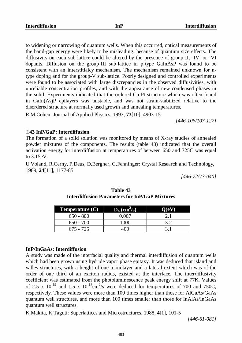
483
Interdiffusion InP Interdiffusion
to widening or narrowing of quantum wells. When this occurred, optical measurements ofthe band-gap energy were likely to be misleading, because of quantum size effects. Thediffusivity on each sub-lattice could be altered by the presence of group-II, -IV, or -VIdopants. Diffusion on the group-III sub-lattice in p-type GaInAsP was found to beconsistent with an interstitialcy mechanism. The mechanism remained unknown for n-type doping and for the group-V sub-lattice. Poorly designed and controlled experimentswere found to be associated with large discrepancies in the observed diffusivities, withunreliable concentration profiles, and with the appearance of new condensed phases inthe solid. Experiments indicated that the ordered Cu-Pt structure which was often foundin GaIn(As)P epilayers was unstable, and was not strain-stabilized relative to thedisordered structure at normally used growth and annealing temperatures.R.M.Cohen: Journal of Applied Physics, 1993, 73[10], 4903-15
[446-106/107-127]
343 InP/GaP: InterdiffusionThe formation of a solid solution was monitored by means of X-ray studies of annealedpowder mixtures of the components. The results (table 43) indicated that the overallactivation energy for interdiffusion at temperatures of between 650 and 725C was equalto 3.15eV.U.Voland, R.Cerny, P.Deus, D.Bergner, G.Fenninger: Crystal Research and Technology,1989, 24[11], 1177-85
[446-72/73-040]
Table 43Interdiffusion Parameters for InP/GaP Mixtures
Temperature (C) Do (cm2/s) Q(eV)650 - 800 0.007 2.1650 - 700 1000 3.2675 - 725 400 3.1
InP/InGaAs: InterdiffusionA study was made of the interfacial quality and thermal interdiffusion of quantum wellswhich had been grown using hydride vapor phase epitaxy. It was deduced that island andvalley structures, with a height of one monolayer and a lateral extent which was of theorder of one third of an exciton radius, existed at the interface. The interdiffusivitycoefficient was estimated from the photoluminescence peak energy shift at 77K. Valuesof 2.5 x 10⁻¹⁹ and 1.5 x 10⁻¹⁸cm2/s were deduced for temperatures of 700 and 750C,respectively. These values were more than 100 times higher than those for AlGaAs/GaAsquantum well structures, and more than 100 times smaller than those for InAlAs/InGaAsquantum well structures.K.Makita, K.Taguti: Superlattices and Microstructures, 1988, 4[1], 101-5
[446-61-081]

484
InSb
Bi
InSb: Bi DiffusionBulk single crystals of In1-xGaxSb1-yBiy (where x was between 0 and 0.21 and y wasbetween 0 and 0.005) were grown onto InSb seed crystals by using a rotary Bridgmanmethod. The quality of the crystals was assessed by using optical microscopic, X-raytopographic, 4-crystal X-ray diffractometric, electron-probe micro-analytical, energy-dispersive spectroscopic, and secondary-ion mass spectroscopic techniques. Due tosegregation, the compositional ratio of Bi increased as the crystals grew. During thegrowth of InGaSbBi, Bi diffused into the InSb seed, and domains of InBi appeared. Forcomparison, InSb1-yBiy (where y was between 0 and 0.05) and In1-xGaxSb (where x wasbetween 0 and 0.16) were grown on InSb. It was found that Bi did not diffuse into InSbwithout Ga, whereas Ga diffused without Bi. The incorporation of Ga produced excess Inand led to the formation of InBi domains.Y.Hayakawa, M.Ando, T.Matsuyama, E.Hamakawa, T.Koyama, S.Adachi, K.Takahashi,V.G.Lifshits, M.Kumagawa: Journal of Applied Physics, 1994, 76[2], 858-64
[446-117/118-189]
Cd
InSb: Cd DiffusionA two-temperature zone method, applied to an InSb substrate plus Cd source system, wasused. The diffusion profiles were determined by using capacitance-voltage measurements,and were similar to those which were habitually found for other III-V systems. Linearplots of junction-depth versus the square root of the diffusion time did not pass throughthe origin. This suggested that the usual interstitial-substitutional model and theconventional Boltzmann-Matano method could not be used to analyze the results. Thediffusivity exhibited a maximum as a function of carrier concentration.S.L.Tu, K.F.Huang, S.J.Yang: Japanese Journal of Applied Physics, 1990, 29[3], 463-7
[446-76/77-029]

485
Ga InSb In
GaInSb: Ga DiffusionBulk single crystals of In1-xGaxSb1-yBiy (where x was between 0 and 0.21 and y wasbetween 0 and 0.005) were grown onto InSb seed crystals by using a rotary Bridgmanmethod. The quality of the crystals was assessed by using optical microscopic, X-raytopographic, 4-crystal X-ray diffractometric, electron-probe micro-analytical, energy-dispersive spectroscopic, and secondary-ion mass spectroscopic techniques. Due tosegregation, the compositional ratio of Ga decreased, as the crystals grew. During thegrowth of InGaSbBi, Ga diffused into the InSb seed. For comparison, InSb1-yBiy (where ywas between 0 and 0.05) and In1-xGaxSb (where x was between 0 and 0.16) were grownon InSb. It was found that Bi did not diffuse into InSb without Ga, whereas Ga diffusedwithout Bi. The incorporation of Ga produced excess In and led to the formation of InBidomains.Y.Hayakawa, M.Ando, T.Matsuyama, E.Hamakawa, T.Koyama, S.Adachi, K.Takahashi,V.G.Lifshits, M.Kumagawa: Journal of Applied Physics, 1994, 76[2], 858-64
[446-117/118-189]
InSb: Ga DiffusionPermeation of Ga was studied by placing an In-Ga-Sb solution in contact with InSbsubstrates under conditions of zero crystal growth. It was found that the permeationdistances were equal to 770, 1270 and 2750µ at 380, 430 and 480C, respectively. It wasdeduced that the apparent diffusivity of Ga ranged from 3 x 10⁻⁷ to 5 x 10⁻⁶cm2/s. Rapidpermeation occurred when the substrate came into contact with the solution.M.Kumagawa, H.Ohtsu, E.Hamakawa, T.Koyama, M.Masaki, K.Takahashi, V.G.Lifshits,Y.Hayakawa: Materials Science and Engineering B, 1997, 44[1-3], 301-3
InSb: Ga DiffusionA 10mm-thick InGaSb crystal was grown onto an InSb seed by using the rotary Bridgmanmethod. It was found that Ga diffused rapidly into the seed and displaced some of the In.The apparent Ga diffusion coefficient was between 10-8 and 10-7cm2/s. These values weremuch higher than the self-diffusion coefficients of In or Sb. Rapid diffusion occurredonly when the substrate was in contact with the solution. The diffusion distance of Gaincreased upon increasing the holding temperature or time.Y.Hayakawa, E.Hamakawa, T.Koyama, M.Kumagawa: Journal of Crystal Growth, 1996,163, 220-5
[446-136/137-125]
In344 InSb: In DiffusionSelf-diffusion in Bridgman-type single crystals was studied, at temperatures ranging from400 to 500C, by using 114mIn radiotracers. An anodic oxidation technique was used for

486
In InSb Li
serial sectioning, and the penetration profiles were fitted to an erf solution of the diffusionequations. It was found that the self-diffusion of In (table 44) could be described by:
D(cm2/s) = 6.0 x 10⁻⁷ [-1.45(eV)/kT]The migration enthalpy of In atoms was estimated to be equal to 0.66eV, and thecorresponding formation enthalpy for an In vacancy was 0.79eV.A.Rastogi, K.V.Reddy: Journal of Applied Physics, 1994, 75[10], 4984-9
[446-117/118-190]
Table 44Diffusivity of 114mIn in InSb
Temperature (C) Diffusivity (cm2/s)414 1.5 x 10⁻¹⁷
435 3.6 x 10⁻¹⁷
449 4.8 x 10⁻¹⁷
457 5.6 x 10⁻¹⁷
477 8.9 x 10⁻¹⁷
500 2.4 x 10⁻¹⁶
345 InSb: In Grain Boundary DiffusionThe self-diffusion of In was studied (table 45) in polycrystalline films by using neutronactivation tracer scanning methods. The grain boundary diffusion parameters wereevaluated at temperatures ranging from 200 to 400C. The data could be described by:
D (cm2/s) = 1.17 x 10⁻⁶ exp[-0.84(eV)/kT]The In diffused via grain boundaries within the temperature range which was studied. Thegrain boundary energy and its temperature dependence was also deduced.A.Rastogi, K.V.Reddy: Semiconductor Science and Technology, 1994, 9[11], 2067-72
[446-119/120-219]
Li
InSb: Li DiffusionThe lithiation of n-type monocrystalline (111)-oriented specimens, via direct reactionwith n-butyllithium in hexane solution, was carried out at room temperature. This processwas monitored by using X-ray diffraction and scanning electron microscope techniques.Resistivity and Hall coefficient data permitted the change in Li concentration to beevaluated. It was deduced that the Li diffusivity at 298K was 1.09 x 10⁻⁸cm2/s.G.Herren, N.E.Walsöe de Reca: Solid State Ionics, 1991, 47[1-2], 57-61
[446-84/85-057]
487
Li InSb Sb
Table 45Grain Boundary Diffusivity of In in InSb
Temperature (C) D (cm2/s)218 2.67 x 10⁻¹⁵
248 7.89 x 10⁻¹⁵
282 2.42 x 10⁻¹⁴
302 4.91 x 10⁻¹⁴
353 1.78 x 10⁻¹³
390 4.53 x 10⁻¹³
413 7.75 x 10⁻¹³
Sb
346 InSb: Sb DiffusionSelf-diffusion in Bridgman-type single crystals was studied, at temperatures ranging from400 to 500C, by using 125Sb radiotracers. An anodic oxidation technique was used forserial sectioning, and the penetration profiles were fitted to an erf solution of the diffusionequations. It was found that the self-diffusion of Sb (table 46) could be described by:
D(cm2/s) = 5.35 x 10⁻⁴ [-1.91(eV)/kT]The migration enthalpy of Sb atoms was estimated to be equal to 0.70eV, and thecorresponding formation enthalpy for an Sb vacancy was 1.21eV.A.Rastogi, K.V.Reddy: Journal of Applied Physics, 1994, 75[10], 4984-9
[446-117/118-190]
Table 46Diffusivity of 125Sb in InSb
Temperature (C) Diffusivity (cm2/s)408 3.9 x 10⁻¹⁸
418 1.2 x 10⁻¹⁷
436 1.5 x 10⁻¹⁷
455 3.2 x 10⁻¹⁷
467 5.3 x 10⁻¹⁷
479 8.7 x 10⁻¹⁷
347 InSb: Sb Grain Boundary DiffusionThe self-diffusion of Sb was studied (table 47) in polycrystalline films by using neutronactivation tracer scanning methods. The grain boundary diffusion parameters wereevaluated at temperatures ranging from 200 to 400C. The data could be described by:
D (cm2/s) = 1.32 x 10⁻⁴ exp[-1.11(eV)/kT]

488
Sb InSb Te
The Sb diffused via grain boundaries within the temperature range which was studied.The grain boundary energy and its temperature dependence was also deduced.A.Rastogi, K.V.Reddy: Semiconductor Science and Technology, 1994, 9[11], 2067-72
[446-119/120-219]
Table 47Grain Boundary Diffusivity of Sb in InSb
Temperature (C) D (cm2/s)218 5.15 x 10⁻¹⁶
248 2.41 x 10⁻¹⁵
256 3.44 x 10⁻¹⁵
282 1.09 x 10⁻¹⁴
310 3.34 x 10⁻¹⁴
350 1.34 x 10⁻¹³
Te
InSb: Te DiffusionA PbTe source was used to grow n-type InSb by means of molecular beam epitaxy. Augerelectron spectroscopic data showed that no surface segregation of Te occurred at dopinglevels of up to about 1019/cm3. Secondary ion mass spectrometry did not reveal thepresence of Pb in the films, even at growth temperatures which were as low as 280C. Thissuggested that the Pb rapidly evaporated from the surface during growth. The secondaryion mass spectrometric depth profiles for Te revealed signs of solid-state diffusion at360C; with a diffusion coefficient of about 10-13cm2/s.D.L.Partin, J.Heremans, C.M.Thrush: Journal of Applied Physics, 1992, 71[5], 2328-32
[446-86/87-046]
489
Author IndexAbe, Y. [440]Abernathy, C.R. [269, 294, 444, 458]Abrosimova, V.N. [292, 323]Acher, O. [439]Adachi, A. [422]Adachi, S. [484, 485]Aers, G.C. [421]Ahlborn, K. [464, 466]Ahlgren, T. [326]Alexandre, F. [398]Algora, C. [250, 355]Allen, E.L. [234, 239, 248, 307,
327, 330, 342, 350]Alsina, F. [431]Alvarez, A.L. [211]Alwan, J.J. [242, 248]Amann, M.C. [373, 419, 438]Amaratunga, G. [318]Ambreé, P. [406, 407, 410, 419]Anderson, G.B. [248, 396]Anderson, S.G. [352]Andersson, M. [277, 304]Andersson, Y. [277, 304]Ando, M. [484, 485]Ansaldo, E.J. [372]Anthony, J.M. [308]Anthony, P.J. [238]Appelbaum, A. [474]Araujo, D. [356, 368]Araujo, G.L. [250, 355]Arent, D.J. [382]Armiento, C.A. [392]Arora, B.M. [428]Asahi, H. [420, 450]
Asashi, H. [433]Ashwin, M.J. [344]Baba, T. [274]Baba-Ali, N. [227, 229, 245, 328,
390, 394]Babievskaya, I.Z. [460, 472]Baeumler, M. [426]Baiocchi, F. [335]Baird, R.J. [412]Baker, J.E. [230, 242, 244, 247, 248,
252, 253, 257, 258, 263, 288, 338, 339, 437, 448]
Balk, P. [473]Bamba, Y. [236]Ban, Y. [263]Bandurko, V.V. [272]Banerjee, S. [428]Bao, X.J. [449]Baranowski, J.M. [399]Baratte, H. [281, 373]Barcz, A.J. [399]Baribeau, J.M. [325]Barker, R.C. [261]Baroni, S. [390]Bársony, I. [343]Bartels, A. [468]Baumann, F.H. [267]Baumeister, E. [247]Baumeister, H. [465]Baur, B. [482]Beall, R.B. [236, 246, 248, 280, 282,
327, 333, 335, 349]Beaumont, B. [416]Beernink, K.J. [248, 262, 264]

Author Index
490
Beggy, J.C. [261]Benchimol, J.L. [405]Bénière, F. [342]Ben-Tzur, M. [359, 473]Benz, K.W. [467]Ber, B.J. [440]Bergner, D. [483]Bernholc, J. [343, 347, 366, 367,
368, 389]Besson, J.M. [313]Bhat, H.L. [450, 453]Bhat, K.N. [363]Bhat, R. [406, 415, 420, 480]Bhattacharya, P. [274, 405]Bhattacharya, P.K. [412]Bimberg, D. [297, 332, 352, 446, 447,
453, 454, 462, 466, 469]Bisberg, J.E. [251, 358, 400]Biswas, D. [274]Bithell, E.G. [392]Blaauw, C. [468, 472, 474]Blanchard, B. [365, 366, 368, 370]Bockstedte, M. [301]Boeringer, D.W. [305]Boesker, G. [363]Bonapasta, A.A. [133]Bonkowski, J.E. [448]Booker, G.R. [423, 427]Borenstein, J.T. [311]Borodina, O.M. [313, 410, 464]Bösker, G. [298, 363, 364]Boudewijn, P.R. [437, 476]Boudreau, R. [245, 249, 339, 361]Bour, B.P. [262, 264]Bour, D. [314]Bour, D.P. [399]Bowen, T. [245, 249, 339, 361]Bradley, I.V. [397, 403, 414, 424, 429]Brandt, O. [465]Braunstein, G. [331]Bravman, J.C. [237, 285, 341, 343]Breitenstein, O. [340, 372, 398, 401]Brewer, J.H. [372]Briggs, A.T.R. [403, 414]Brillouet, F. [391, 398]Brion, H.G. [464, 466]Briones, F. [447]Bronner, W. [237]
Bruk, A.S. [313]Brum, J.A. [408, 412]Buchanan, M. [421]Budko, T.O. [476]Bühlmann, H.J. [456]Burke, P.T. [395]Bürkner, S. [396, 424, 426]Burnham, R.D. [234, 243, 244, 245,
247, 249, 252, 256, 338]Burri, G. [368]Burton, R.S. [243, 245]Busygina, L.A. [440]Butherus, A.D. [335]Cahen, D. [477]Cai, D.Q. [395]Calawa, A.R. [388]Calle, F. [211, 465]Calleja, J.M. [432]Camassel, J. [431]Caneau, C. [266, 267, 415, 469, 480]Cannelli, G. [294]Cantelli, R. [294]Capizzi, M. [133, 294]Cardona, M. [302, 447]Cardone, F. [281, 373]Carlin, J.F. [456]Carr, N. [434]Caruso, R. [277]Castagné, J. [236, 246, 248, 280, 282,
327, 333, 335, 349]Cerny, R. [483]Chan, L.Y. [359, 366, 473, 480]Chan, W.K. [406]Chand, N. [238]Chang, C.C. [406]Chang, C.S. [37]Chang, J.C.P. [233, 346]Chang, K.H. [274, 287, 345]Chang, K.J. [289]Chang, S.K. [470]Chang, T.C. [287]Chang, T.Y. [267]Chang, Y.A. [400]Chaplain, R. [342, 459]Charbonneau, S. [421]Chase, M.P. [302, 362]Chatterjee, B. [463]Chatterjee, S. [363]

Author Index
491
Chavignon, J. [391]Chayahara, A. [319, 324, 325]Chen, A.C. [448]Chen, B. [343, 347, 389]Chen, C.H. [175]Chen, C.Y. [364]Chen, E.I. [253]Chen, H.R. [394]Chen, P. [398]Chen, S. [331]Chen, W.C. [37]Chen, Y. [364, 391]Chen, Y.C. [405]Cheng, C.L. [462]Cheng, K.Y. [448]Cheng, W.H. [474]Cheong, B.H. [289]Chester, M.J. [324]Chevallier, J. [238, 241, 294, 295,
310, 312, 313, 314, 454, 460]Chi, P.H. [266, 267, 286, 309, 315, 341,
364, 415, 459, 463, 467, 469]Chia, V.F.K. [234, 239, 248]Chin, A.K. [251, 355, 358, 400]Chiu, T.H. [336, 337, 338, 357, 386]Cho, K.I. [377, 422]Choa, F.S. [473]Choe, B.D. [83, 428]Choi, J.S. [470]Chow, D.H. [443]Chow, K. [372]Chow, K.H. [371]Christen, J. [332]Chu, S.N.G. [478, 479]Chui, T.H. [331]Cibert, J. [392]Clarke, R. [274]Clegg, J.B. [236, 246, 248, 280, 282,
327, 333, 335, 349]Clemencon, J.J. [355]Cockayne, D.J.H. [395]Cockerill, T.M. [242, 248]Cohen, D.D. [350]Cohen, P.I. [231, 374, 375]Cohen, R.M. [17, 298, 315, 364,
388, 393, 395, 483]Colas, E. [228, 254]Coldren, L. [250, 359]
Coldren, L.A. [244, 250, 455]Coleman, J.J. [242, 248]Conibeer, G.J. [451, 452]Corbett, J.W. [311]Cordero, F. [294]Corzine, S. [244, 250]Cox, H.M. [406]Cox, S.F.J. [372]Craford, M.G. [230, 263, 437]Craighead, H.G. [275]Cremer, C. [482]Crook, A. [242, 248]Cunningham, B.T. [256, 262, 288]Cunningham, J.E. [331, 336, 337, 338]Cunningham, T.J. [261]Cutlerywala, H. [364]Dabiran, A.M. [231, 374, 375]Dabkowski, F.P. [251, 358, 400]Dabrowski, J. [304, 342, 344]Dadgar, A. [466]Dagata, J.A. [324]Dallesasse, J.M. [243, 249, 257]Dandrea, R.G. [389]Danilewsky, A.N. [467]Dautremont-Smith, W.C. [294, 461, 464]Davies, G.J. [405]Däweritz, L. [384]De Cremoux, B. [361]De Souza, J.P. [281]De, T.J. [359]Deal, M.D. [234, 237, 239, 248, 282,
283, 285, 286, 302, 303, 307, 318,327, 329, 330, 334, 341, 342, 343,
350, 362]Deicher, M. [290]Deppe, D.G. [230, 252, 253, 256, 257,
258, 263, 338, 339, 360, 437]Descouts, B. [391]De Temple, T.A. [242, 248]Deus, P. [483]Dhanasekaran, R. [278]Dieckmann, R. [270]Dieguez, E. [450]Dietrich, H.B. [286, 309, 341, 415,
459, 463, 467, 469]Dildey, F. [419]Dion, M. [421]Dixon, R.H. [470]

Author Index
492
Dodds, S.A. [372]Dos Passos, W. [274]Dreybrodt, J. [432]Dreyer, K. [386]Dubon-Chevallier, C. [405]Duke, C.B. [389]Dunsiger, S.R. [371]Dunstan, D.J. [429]Dutta, P.S. [450, 453]Duvarney, R.C. [372]Dzhumakulov, D.T. [321]Eastman, L.F. [283]Ebbinghaus, G. [419]Eberl, K. [302]Ebert, P. [448]Eccleston, R. [392]Eger, D. [468, 474, 477]Egger, U. [340, 372, 398, 401]Egilsson, T. [317]Eizenberg, M. [290]Elman, B. [392]El-Zein, N. [243, 249, 319]Emanuel, M.A. [248]Emelyanenko, J.S. [476]Emeny, M.T. [429]Emmerstorfer, B. [472]Emura, S. [433, 450]Enders, P. [480]Endicott, F.J. [347, 396, 399]Endoh, A. [236]Enquist, P. [359]Epler, J.E. [234, 256, 347]Erickson, J.W. [302, 447]Erofeeva, E.A. [321]Estle, T.L. [314, 371, 372]Fahy, M.R. [344]Fan, J.C. [287, 345, 427]Fareed, R.S.Q. [278]Farley, C.W. [308]Fathimulla, A. [286, 309, 341, 459,
463, 467]Favennec, P.N. [459]Fedotov, A.B. [321]Fenninger, G. [483]Fewster, P.F. [344]Fischer, A. [302]Flat, A. [332]Fleischman, A.J. [373]
Fletcher, R.M. [230, 263, 437]Fons, P. [457]Fonstad, C.G. [406, 413, 414]Fontijn, G.M. [435, 436, 437, 438,
439, 462, 463, 470, 475]Forchel, A. [432, 433]Fornari, R. [103]Forster, T. [382]Franke, D. [461]Franz, G. [373, 438]Franzheld, R. [398, 401]Freundlich, A. [348]Frova, A. [294]Fujii, E. [346]Fujii, M. [377]Fujii, N. [369]Fujii, S. [371]Fujii, T. [236]Fujii, Y. [324]Fujita, K. [340, 377, 426]Fukunaga, T. [252, 332]Furtado, M.T. [396, 409, 411, 417,
418, 426]Furuya, A. [258]Gailhanou, M. [368]Gal, M. [395]Ganière, J.D. [245, 328, 356, 365,
366, 368, 370]Gao, Y. [391, 398]García, S. [465]Gauneau, M. [342, 459]Gautam, D.K. [290, 365]Gautier, S. [404]Gavand, M. [294]Gavrilovic, P. [244, 247, 258, 338]Gaymann, A. [237]Genut, M. [290]George, T. [348]Geva, M. [238, 420, 478, 479]Ghaffari, M. [466]Giannelis, E.P. [351]Giannozzi, P. [311]Gibala, R. [274]Gibart, P. [241, 310]Gibbons, J.F. [360]Gilderman, V.K. [269]Gillin, W.P. [397, 399, 403, 414,
424, 429, 430, 432]

Author Index
493
Giovine, E. [294]Gisdakis, S. [319]Gislason, H.P. [293, 317]Glade, M. [472, 473]Glew, R.W. [431]Goldberg, R.D. [421]Gonda, S. [433, 450]González-Díaz, G. [465]Gorelenok, A.T. [440]Gösele, U. [237, 241, 252, 261, 277,
280, 283, 291, 297, 298, 300, 301,305, 333, 336, 344, 345, 346, 354,360, 367, 372, 398, 401, 461, 481]
Goto, K. [417]Goto, S. [238, 281, 379, 380, 387]Govorkov, A.V. [313]Grandjean, N. [387]Grant, J. [390]Grattepain, C. [348, 454]Grattepain, C.M. [238, 294]Grenet, J.C. [348]Griehl, S. [293]Griffin, P.B. [318]Grigorev, N.N. [361]Grodkiewicz, W.H. [335]Grote, N. [461]Gruen, N. [237]Gruenbaum, P.E. [452]Grundmann, M. [332]Gruska, B. [406, 407, 419]Grützmacher, D. [433, 473]Gudmundsson, J.T. [317]Guersen, R. [1]Guido, L.J. [234, 244, 247, 252, 256,
259, 261, 262, 288, 338]Guillaume, J.C. [416]Gulwadi, S.M. [415, 469]Guoba, L.B. [278, 300]Gushchinskaya, E.V. [476]Gwilliam, R. [392, 397, 424]Gyuro, I. [432]Ha, J.S. [386]Ha, N.T. [357, 473, 478, 479]Haddara, Y.M. [285]Hafich, M.J. [265]Haga, D. [357]Haga, T. [456]Hailemariam, E. [266, 267, 405, 414]
Hallali, P.E. [281]Haller, E.E. [297, 302, 359, 366,
372, 447, 473, 480]Hamakawa, E. [484, 485]Hamakawa, Y. [292]Hamilton, W.J. [443]Hamoudi, A. [441]Han, H.T. [245, 249, 339, 361]Hangleiter, A. [407, 410, 419]Hanson, C.M. [359, 473]Hara, N. [242, 306, 345, 390]Hara, T. [289]Harada, Y. [346]Harbison, J.P. [227]Harde, P. [461]Hardingham, C.M. [451, 452]Harper, J. [386]Harris, G.L. [283]Harris, J.J. [236, 246, 248, 280, 282,
327, 333, 335, 349]Harris, J.S. [407, 411]Harrison, I. [227, 229, 230, 245,
328, 390, 394]Hart, L. [344]Harun-ur Rashid, A.B.M. [351]Hashimoto, A. [252, 332]Hashimoto, H. [258, 284, 338]Haspeklo, H. [415, 475]Hata, M. [376, 387]Haukson, I.S. [317]Hawkins, R.L. [279]Hayakawa, Y. [484, 485]Haynes, T.E. [342]Heime, K. [433]Heine, K. [472]Heinecke, H. [482]Heinz, C. [451, 452]Heitz, R. [466]Helms, C.R. [340]Henini, M. [227, 229, 230, 245, 328]Heremans, J. [488]Hergeth, J. [473]Herms, M. [293]Hernandes, C.S. [351]Herren, G. [486]Herring, C. [314, 315]Herzinger, C.M. [242, 248]Herzog, L. [340]

Author Index
494
Hesse, R. [354]Hettwer, H.G. [340, 353, 363, 364, 470]Heuken, M. [433]Heurtel, A. [312]Higashisaka, A. [289]Higuchi, M. [471]Hill, D.M. [352]Hillard, R.J. [449]Hillmer, H. [423]Hira, K. [319]Hirai, K. [323, 324, 325]Hirai, M. [340]Hitti, B. [371]Hiyamizu, S. [422]Ho, H.P. [227, 229, 230, 394]Hobbs, L. [468, 472]Hobson, W.S. [266, 267, 405, 414]Hockly, M. [423]Hoepfner, A. [319]Höfler, G.E. [243, 261, 319]Hofsäss, V. [423]Holland, O.W. [415, 469]Holmgren, D.J. [243, 245]Holonyak, N. [230, 234, 243, 244, 247,
249, 252, 253, 256, 257, 258, 261,262, 263, 288, 319, 338, 339,
360, 437]Homewood, K.P. [397, 399, 403, 414,
424, 429, 432]Hong, C.Y. [389]Hong, J.M. [275]Hong, S.K. [440]Hong, W.P. [415, 469, 480]Hopkins, L.C. [279]Höpner, A. [471]Horikoshi, Y. [254, 315, 375, 377, 384]Horino, Y. [319, 325]Houde-Walter, S.N. [256, 258, 259, 260]Houdré, R. [456]Hovel, H.J. [373]Howard, A.J. [265]Howard, L.K. [397, 424, 429]Hsieh, K.C. [234, 243, 247, 252, 256,
257, 258, 261, 319, 320, 360, 448]Hsieh, K.Y. [260, 409, 412]Hsu, C.C. [443]Hsu, J.T. [292]Hsu, L. [302, 447]
Hu, E. [250, 359]Hu, E.L. [175, 244, 250]Hu, J.C. [285, 286, 303]Hu, P. [393]Huang, J.H. [267]Huang, K.F. [484]Huang, L.J. [325]Hughes, O.H. [230]Hult, M. [277, 304]Humer-Hager, T. [288, 369]Hutchby, J.A. [359]Hwang, D.M. [415, 420]Hwang, Y. [355]Hwang, Y.L. [409, 412]Hyeon, J.Y. [466]Ichimura, K. [250]Iguchi, H. [233]Iikawa, F. [408, 412]Ikarashi, N. [274]Ikeda, H. [295]Ilegems, M. [456]Imamura, Y. [420]Inai, M. [286, 342]Inohara, H. [319]Inoue, Y. [299]Ishibashi, A. [263]Ishii, K. [236]Ishikawa, H. [236]Ishino, M. [418]Isu, T. [376, 380, 387]Ito, H. [242, 398, 401, 411, 481]Ito, R. [445]Ito, T. [255, 378]Itoh, H. [242]Itoh, M. [435, 441]Ivanov, S.V. [235, 281]Jach, T. [324]Jackman, T.E. [421]Jackson, T.N. [373]Jacobs, J.M. [438, 475]Jaeger, W. [363]Jafri, Z.H. [430]Jagadish, C. [395]Jäger, W. [298, 305, 353, 363, 364, 470]Jaklevic, J. [366, 480]Jaklevic, J.M. [359, 473]Jalil, A. [312]James, D.J. [326]
Author Index
495
Jan, W. [331, 338]Janzén, E. [317]Jeanjean, P. [347]Jeong, B.S. [442]Jeong, W.G. [428]Jiménez, J. [103]Johnson, M.B. [284]Johnson, N.M. [314, 315, 407, 411]Jones, K.S. [307, 330, 341, 342, 350]Jordan, A.S. [238]Joullie, A. [455, 457]Joyce, B.A. [231]Juhel, M. [441]Kadono, R. [371, 372]Kahen, K.B. [239, 249, 334, 358,
360, 367, 393]Kakinoki, H. [295]Kalem, S. [454]Kalish, R. [290]Kaliski, R.W. [234, 252, 256]Kamanin, A.V. [440, 477]Kamei, H. [457]Kamei, K. [426]Kamejima, T. [307]Kameneckas, J.V. [278, 300]Kaminska, M. [460]Kamiya, T. [431]Kanber, H. [283, 291, 320]Kaneko, Y. [242]Kang, B.K. [439]Kang, T.W. [389]Kano, H. [232, 387]Karenina, L.S. [269]Karlicek, R.F. [478]Karttunen, V. [312]Kasai, K. [306, 345]Kasu, M. [232, 380, 385, 386]Katahama, H. [426]Kataoka, M. [456]Kataoka, Y. [236]Katayama, M. [299]Katayama, Y. [379, 380, 387]Katoda, T. [351, 390]Katsumata, H. [113]Kavanagh, K.L. [316, 322, 346, 348]Kawabe, M. [280, 329]Kawaguchi, Y. [420]Kawai, T. [316]
Kawamura, Y. [420]Kawashima, M. [254, 375, 377, 384]Kazarina, N.N. [460, 472]Kazmierski, C. [476]Kazmierski, K. [361]Kehr, K.W. [374]Keinonen, J. [312, 326]Keller, R. [290]Keller, R.C. [340]Kempeners, M.N.C. [476]Ketata, K. [403, 404, 405]Ketata, M. [403, 404, 405]Khald, H. [455, 457]Khoo, G.S. [382]Khreis, O.M. [399]Kidoguchi, I. [263]Kiefl, R.F. [371, 372]Kim, I. [428]Kim, J.G. [446]Kim, J.H. [439]Kim, M.S. [333]Kim, S.G. [450]Kim, S.K. [389]Kim, S.T. [442]Kim, T.S. [308]Kim, T.W. [389]Kim, Y. [333, 395]Kim, Y.H. [389]Kimura, T. [369, 431]Kirchner, P.D. [346]Kish, F.A. [243, 247, 249, 258, 339]Kishi, M. [351]Kishimoto, D. [381, 385, 456]Kisielowski, C. [388]Kitada, T. [422]Klein, P.B. [286, 309, 341, 459,
463, 467]Klem, J.F. [265]Klöber, J. [293]Klockenbrink, R. [468]Knecht, A. [297, 352, 446, 447, 453,
454, 462, 469]Ko, K.Y. [331]Kobayashi, J. [284, 338]Kobayashi, N. [232, 380, 385, 386]Kobayashi, T. [481]Koch, M.W. [288]Koehler, K. [237]
Author Index
496
Koenraad, P.M. [284, 343]Kohnke, G.E. [288]Kohzu, H. [289]Kolbas, R.M. [260, 355, 409, 412]Koltsov, G.I. [284, 459]Komeno, J. [306, 345]Kondo, E. [376]Kondo, S. [435, 441]König, U. [415, 475]Koo, J.Y. [386]Kopev, P.S. [235, 281]Kopf, R.F. [244, 279]Koponen, I. [312]Korbutyak, D.N. [293]Korobkov, N.N. [292, 323]Koshiba, S. [232, 387]Koszi, L.A. [461, 464]Koteles, E.S. [392]Kothiyal, G.P. [412]Koumetz, S. [403, 404, 405]Koyama, T. [484, 485]Koza, M. [415, 420]Koza, M.A. [480]Kozhukhova, E.A. [410, 464]Kozlovskii, V.V. [292, 323]Krames, M.R. [253]Kraus, G.T. [351]Kräutle, H. [297, 352, 446, 447, 453,
454, 462, 469]Krauz, P. [391, 398, 402, 410, 413, 441]Kreitzman, S.R. [372]Kreller, D. [472]Krieghoff, T. [471]Kringhøj, P. [469]Kristjánsson, S. [317]Kubena, R. [393]Kucera, J. [321]Kudykina, T.A. [361]Kuech, T.F. [235, 240]Kühn, G. [354, 355, 471]Kuhn, J. [423]Kuisl, M. [415, 475]Kumagai, M. [323, 324]Kumagawa, M. [484, 485]Kumagaya, M. [319, 325]Kumar, V. [453]Kuo, C.P. [230, 263, 437]Kuo, J.M. [244, 279]
Kuo, T.Y. [331]Kupka, R.K. [391]Kurishima, K. [481]Kuriyama, Y. [276, 301]Kuroda, S. [242]Kusano, C. [238, 281]Kuttler, M. [466]Kuwamoto, H. [474]Kuzuhara, M. [307]Kwiatkowski, S. [399]Kwon, H.K. [83]Kwon, O. [439, 440]Kwon, Y.S. [251]Kwon1, S.D. [83]Ky, N.H. [245, 328, 356, 365,
366, 368, 370]Lagally, M.G. [448]Lahiri, I. [1, 233]Lakdawala, V.K. [292]Landgren, G. [253, 317, 353, 466]Landheer, D. [325]Lanzillotto, A.M. [246, 334]Larkins, E.C. [396, 424, 426]Laruelle, F. [393]Lashkevich, L.N. [293]Lau, W.M. [325]Launay, F. [361, 439]Launay, P. [403, 404, 405]Launois, H. [391]Lauterbach, C. [469]Lawrence, D.J. [239, 251, 357, 358, 400]Ledentsov, N.N. [235, 281]Lee, C. [333, 342]Lee, C.C. [237, 285, 341, 342, 343]Lee, C.P. [287, 345, 394, 427]Lee, E. [386]Lee, E.H. [440]Lee, J.C. [235, 240]Lee, J.H. [260, 409, 412]Lee, J.I. [470]Lee, J.K. [440]Lee, J.L. [280, 329]Lee, J.Y. [440]Lee, K.H. [329, 437, 438, 440]Lee, S. [386]Lee, S.C. [37, 287]Lee, S.H. [394, 427]Lee, S.T. [251, 261, 305, 331, 357, 400]

Author Index
497
Lee, Y.T. [439, 440]Lefebvre, F. [404]Leitch, A.W.R. [310, 311]Lengel, G. [386]Lennard, W.N. [325, 477]Leon, R.P. [460]Leonard, D. [455]Lester, S.D. [308]Lesunova, R.P. [269]Leycuras, A. [348]L'Haridon, H. [459]Li, E.H. [433]Li, W. [482]Li, W.M. [315]Li, Y.J. [275, 307]Liau, Z.L. [465]Lichti, R.L. [314, 371, 372]Lifshits, V.G. [484, 485]Likonen, J. [326]Liliental-Weber, Z. [388, 460]Lim, H.J. [470]Lim, H. [83]Lin, H.H. [287]Lin, Z. [352]Lindeberg, I. [277, 304]Linnarsson, M. [317]Linnarsson, M.K. [253, 317, 353, 357]Liou, D.C. [287, 345]Liu, B.D. [287]Liu, D.G. [287, 345]Liu, H. [446]Lo, V.C. [339]Lo, Y.C. [260]Logan, R.A. [478, 479]Logan, R.C. [294]Lomasov, V.N. [292, 323]Long, J. [462]Long, N.J. [423, 427]Lopata, J. [294, 449, 461, 464]López, M. [379]Lord, S.M. [407, 411]Lösch, R. [423]Loural, M.S.S. [396, 418, 426]Ludowise, M.J. [230, 263, 437]Ludwig, M.H. [446]Luftman, H.S. [266, 267, 279, 357,
405, 414]Luken, K.M. [277]
Lunardi, L.M. [244]Luo, Y.S. [383]Lusson, A. [454]Lyahovitskaya, V. [477]Lyubomirsky, I. [477]MacFarlane, A. [371]Machayekhi, B.[238, 241, 294, 310,314]Machayekhi, D. [313]Maehara, Y. [426]Magee, C.W. [246, 316, 322, 348]Magerle, R. [290]Maier, M. [237, 396, 424]Major, J.S. [256, 262, 288]Makarov, V.V. [284, 459]Makita, K. [483]Malin, J.I. [448]Malkovich, R.S. [320]Mallard, R.E. [423, 427]Malyshev, S.A. [476]Mani, H. [455, 457]Mannoh, M. [263]Marbeuf, A. [294]Marcon, J. [403, 404, 405]Marek, H.S. [477]Marenkin, S.F. [460, 472]Marfaing, Y. [312]Marschall, P. [415, 475]Marti, A. [250, 355]Mártil, I. [465]Martin, J.M. [266, 267, 465]Martin, P. [404]Martin, R.W. [434]Masaki, M. [485]Masseli, K. [473]Massies, J. [387]Masut, R.A. [408, 412]Matsuhata, H. [457]Matsui, T. [406, 440, 460]Matsui, Y. [418]Matsumoto, S. [435, 441]Matsumura, N. [456]Matsushita, A. [371]Matsushita, S. [346]Matsuyama, T. [484, 485]Matyi, R.J. [247, 360]Matz, R. [482]Meglicki, Z. [350]

Author Index
498
Mehrer, H. [353, 363, 470]Mei, P. [227, 228, 415, 420]Meier, H.P. [382]Melchior, H. [361]Melloch, M.R. [1, 233]Melman, P. [392]Méndez, B. [450]Mendonça, C.A.C. [386]Menéndez, J. [390]Merkulov, A.V. [440]Merlin, R. [274]Merz, J. [393]Merz, J.L. [244, 245, 249, 250,
339, 359, 361]Mestres, N. [274, 432]Meyer, J.W. [316, 322, 348]Micallef, J. [433]Migitaka, M. [295, 296]Mihashi, Y. [417]Miles, R.H. [443]Milnes, A.G. [449]Miloche, M. [241, 310, 314, 460]Min, S.K. [333]Minervini, A.D. [253]Mishima, T. [238]Mitchell, I.V. [421]Mitev, P. [259]Mitra, S. [274, 306]Mitsuhara, M. [435, 441]Mitsui, S. [369]Miyauchi, E. [284, 338]Miyoshi, S. [445]Mizuta, M. [447]Mochizuki, A. [289]Mochizuki, K. [238, 281, 286, 289,
377, 422]Mochizuki, Y. [447]Moise, T.S. [261]Mokina, I.A. [440, 477]Molinari, E. [390]Montie, E.A. [475]Moon, D.C. [442]Moore, W.J. [279]Morgenstern, T. [355]Mori, H. [324]Mori, M. [242]Morishita, Y. [379, 380, 387]Morita, T. [284, 338]
Moriya, N. [290]Morrow, R.A. [277, 311, 322]Moseley, A. [434]Motisuke, P. [408, 412]Mui, D.S.L. [245, 249, 339, 361, 455]Mukai, K. [395, 432]Mukai, S. [242]Müller, G. [270]Mulpuri, S. [415, 469]Murata, M. [431]Murray, J.J. [307, 327, 330, 334,
348, 350]Murray, R. [335]Murrell, D.L. [416]Musbah, O.A. [400]Muto, S. [456]Nadella, R.K. [266, 267]Nagahara, M. [445]Nagamine, K. [371]Nagamune, Y. [232, 387]Nagano, J. [276, 301]Nakajima, K. [403, 408, 421]Nakamura, M. [296]Nakamura, T. [286, 289]Nakamura, Y. [232, 250, 387, 401]Nakanishi, H. [319]Nakano, Y. [290, 365]Nakashima, K. [420, 433]Nakata, Y. [456]Nam, D.W. [244, 247, 256, 338, 360]Nam, E.S. [439]Näser, A. [466]Nashelskii, A.Y. [410, 464]Nassibian, A.G. [350]Navratil, K. [321]Nazar, L. [415, 420]Neave, J.H. [231]Nekado, Y. [296]Nelson, R.W. [459]Neugebauer, J. [445]Neumann, R. [319]Newman, R.C. [322, 335, 344]Ng, I. [433]Nicholas, R.J. [434]Niedermayer, C. [372]Niklas, J.R. [293]Nilsson, S. [382]Nishida, K. [325]
Author Index
499
Nishinaga, T. [276, 302, 374, 375, 376,377, 380, 381, 385, 422,
455, 456, 467]Nishino, T. [292]Nishiyama, K. [371]Noack, M. [374]Noda, T. [232, 387]Noge, H. [232, 387]Nolte, D.D. [1, 233]Nomura, Y. [379, 380, 387]Norcott, M. [281]Nordell, N. [253, 317, 353]Nörenberg, H. [384]Norman, A.G. [427]Northrup, J. [344]Northrup, J.E. [299, 304, 306, 342, 345]Novikova, V.V. [410, 464]Nowak, E. [354, 355, 471]Nozaki, S. [327, 348]Nozaki, T. [307]Nukui, T. [242]Nutt, H.C. [326]O’Reilly, E.P. [396, 424]Ogasawara, Y. [316]Ogata, H. [406, 460]Ogihara, M. [401]Oh, J.E. [274]Oh, Y.T. [389]Ohfuji, S. [276, 301]Ohishi, T. [440]Ohnaka, K. [263]Ohnishi, H. [340]Ohno, T. [255]Ohori, T. [306, 345]Ohsawa, J. [295, 296]Ohtsu, H. [485]Ohtsuka, K. [440]Ohtsuka, K.I. [406, 460]Oikawa, H. [289]Ojala, P. [253, 317, 353]Okamoto, Y. [467]Olmsted, B.L. [256, 258, 259, 260]Omelyanovskii, E.M. [313, 410, 464]Omura, E. [244, 250, 359, 417]Onabe, K. [445]Ong, C.K. [382]Ono, H. [274]Osentowski, T.D. [230, 263, 437]
Osgood, R.M. [321]Oshinowo, J. [432, 433]Ossart, P. [391, 398, 402, 410, 413]Ostling, M. [277, 304]Osvald, J. [388]Otsuka, N. [418]Ougazzaden, A. [441]Ourmazd, A. [267]Oyanagi, H. [457]Paine, B.M. [283]Pajot, B. [294, 295]Pak, K. [316]Pakhomov, A.V. [313, 410, 464]Palguev, S.F. [269]Palma, A. [379]Pan, H. [482]Paoli, T.L. [234, 252, 256, 347]Parguel, V. [459]Park, H.H. [437, 438, 439, 440]Park, H.L. [442, 470]Park, R.M. [446]Parker, S.M. [462]Partin, D.L. [488]Pascual, J. [431]Pashkova, O.N. [460, 472]Paska, Z.F. [357]Pass, C.J. [234, 239, 248]Pavesi, L. [245, 311, 328, 356, 368]Pearton, S.J. [63, 266, 267, 269, 277,
294, 311, 405, 414, 444,449, 458, 461, 464]
Pechman, R.J. [383]Peiner, E. [468]Perenboom, J.A.A.J. [343]Perley, A.P. [266, 267, 405, 414]Perrin, S.D. [432]Peskov, N.V. [380]Peterson, D.L. [239, 393]Petrich, G.S. [231, 374, 375]Petroff, P.M. [275, 307, 392, 393, 455]Pétursson, J. [317]Peyre, H. [431]Pfeiffer, L. [246]Pfeiffer, L.N. [390]Pfeiffer, W. [290]Pfister, J.C. [366]Pfiz, T. [372]Phillips, C. [392]

Author Index
500
Pilkuhn, M.H. [407, 410, 419]Pinzone, C.J. [478]Piqueras, J. [450]Pisarev, A.A. [272]]Planel, R. [347, 391]Plano, W.E. [230, 234, 244, 247, 256,
257, 258, 263, 338, 360, 437]Ploog, K. [384]Plummer, J.D. [234, 239, 248, 285, 286,
302, 303, 307, 318, 330,350, 362]
Polyakov, A.J. [313]Polyakov, A.Y. [410, 449, 464]Ponce, F.A. [347, 396, 399]Poole, P.J. [421]Poroikov, J.A. [460, 472]Potter, T.J. [412]Pozsgai, I. [293]Prescha, T. [310, 311]Primig, R. [482]Pross, P. [290]Pudenzi, M.A.A. [351]Quillec, M. [402, 410, 413]Quintana, V. [355]Rahbi, R. [238, 241, 294, 314]Rai-Choudhury, P. [449]Räisänen, J. [312, 326]Rajatora, M. [326]Rajeswaran, G. [239, 358, 367, 393]Ralston, J.D. [396, 424, 426]Ramasamy, P. [278]Rao, E.V.K. [391, 398, 402, 410,
413, 441]Rao, K. [441]Rao, M.V. [266, 267, 286, 309, 341,
415, 459, 463, 467, 469]Rao, P.R.S. [363]Rao, S.S. [403, 414]Rastogi, A. [486, 487, 488]Ravich, V.N. [460, 472]Razeghi, M. [439]Reddy, K.V. [486, 487, 488]Reddy, V. [342]Redinbo, G.F. [275]Rees, P.K. [326]Régrény, A. [342]Reinhart, F.K. [245, 328, 356, 365,
366, 368, 370]
Ren, H.W. [302]Renner, D. [474]Rentschler, J.A. [267]Reynolds, C.L. [420]Reynolds, S. [360]Richard, T.A. [243, 249]Rihet, Y. [459]Ringel, S.A. [463]Riseman, T.M. [372]Robbins, V.M. [257]Robert, J.L. [347]Roberts, C. [236, 246, 248, 280,
327, 349]Robinson, D. [270]Robinson, H.G.[282, 283, 318, 341, 342]Robinson, W. [393]Rodionov, A.I. [321]Roedel, R.J. [364, 459]Roos, G. [315, 407, 411]Rose, B. [460]Roth, A.P. [408, 412]Rothemund, W. [396, 424, 426]Rubart, W.S. [307, 330, 350]Rucki, A. [353, 363, 364, 470]Rudra, A. [456]Ruf, T. [447]Rytova, N.S. [310]Ryu, S.W. [428]Sacilotti, M.A. [408, 409, 411, 412,
417, 418]Sacks, R.N. [261]Sadana, D.K. [281]Sai, N. [394]Saito, D. [316]Saito, R. [431]Sajoto, T. [335]Sakaguchi, M. [319, 323, 324]Sakai, S. [251]Sakaki, H. [232, 387]Sakakibara, K. [418, 471, 475, 479]Sakalas, A.P. [278, 300]Salemink, H.W.M. [284]Sallese, J.M. [456]Salmeron, M. [233]Sandrik, R. [388]Sano, N. [422]Santos, M. [246, 334, 335]Sapriel, J. [391, 398]
Author Index
501
Sargünas, V.R. [278, 300]Sasa, S. [236]Satho, M. [319, 325]Sato, E.A. [409, 411, 417, 418]Sauer, N.J. [279]Scarrott, K. [427]Schad, R.G. [281]Schade, U. [479, 480]Schaff, W.J. [283]Schauer, S.N. [459]Scheffler, M. [301]Schier, M. [419]Schlaak, W. [297, 352, 446, 447, 453,
454, 462, 469]Schlachetzki, A. [468]Schlapp, W. [423]Schlesinger, T.E. [235, 240, 243,
245, 449]Schlotter, N.E. [406]Schmidt, H.J. [472]Schmidt, M.T. [321]Schneider, M. [391]Schneider, W. [372]Scholz, R. [372, 398]Schowalter, L.J. [381]Schubert, E.F. [244, 246, 279, 336,
337, 478]Schultz, M. [277, 372, 398, 401]Schulz, K.J. [400]Schumann, B. [354, 355, 471]Schumann, D. [371]Schumann, H. [466]Schützendübe, P. [384]Schwab, C. [314, 371, 372]Schwartz, B. [335]Schwartz, C.L. [228, 415, 420]Schwarz, S.A. [227, 228, 415, 420, 480]Schweizer, H. [423]Scilla, G.J. [373]Scott, E.G. [405, 423]Sealy, B.J. [429, 467]Sekiguchi, Y. [418, 471, 475]Seko, M. [418, 475]Sellitto, P. [347]Semprini, E. [379]Serreze, H.B. [477]Seshadri, S. [259, 261]Seta, M. [450]
Shacham-Diamand, Y. [351]Shah, D.M. [406]Shahar, A. [254]Shapira, Y. [352]Sharma, V.K.M. [451, 452]Shayegan, M. [246, 334, 335]Sheets, J. [316, 322, 348]Shen, X.Q. [375, 380, 381, 385,
455, 456]Shepherd, F.R. [468, 474, 477]Shi, S.S. [245, 249, 339, 361]Shiba, Y. [426]Shichijo, H. [247, 360]Shieh, T.H. [287]Shiina, K. [306, 345]Shimogaki, Y. [365]Shimomura, S. [422]Shinoda, A. [286, 342]Shintani, Y. [251]Shiomi, A. [323, 324]Shiraishi, K. [255, 376, 378]Shiraki, Y. [445]Shitara, T. [231, 376, 377, 422]Shiu, W.C. [433]Shmidt, N.M. [440, 477]Sicart, J. [347]Siefert, R.L. [383]Siegel, W. [293]Siethoff, H. [464, 466]Silveira, J.P. [447]Simes, R. [393]Simons, D.S. [266, 267, 286, 309, 315,
341, 364, 415, 459, 463, 467, 469]Sin, Y.K. [355]Singh, J. [274, 405]Singh, S. [335]Skoryatina, E.A. [320]Skromme, B.J. [415, 420]Skudlik, H. [290]Slotte, J. [326]Smirnov, V.M. [272]Smith, A.D. [403, 414]Smith, F.T. [251, 357, 400]Smith, R.S. [326]Smith, S.C. [243, 245, 249]Sobotta, H. [354]Södervall, U. [298, 364]Solmon, H. [270]

Author Index
502
Somogyi, K. [241, 293, 310]Song, J.I. [480]Soni, R.K. [450]Sonoda, T. [369]Speier, P. [432]Spence, J.P. [367]Spencer, M.G. [283]Spiller, G.D.T. [405]Springthorpe, A.J. [472, 477]Srivastava, A.K. [428]Stähl, K. [277, 304]Stam, M. [449]Stark, J.B. [336]Stavola, M. [461, 464]Steckl, A.J. [398]Sternitzke, M. [270]Stevenson, D.A. [282, 318, 327, 329,
334, 437, 438]Stillman, G.E. [256, 262, 288]Stobbs, W.M. [392]Stollenwerk, M. [433]Stolwijk, N.A. [298, 353, 363, 364, 470]Storz, F.G. [386]Streetman, B.G. [308]Stutius, W. [258]Stutzmann, M. [454]Suehiro, H. [242]Sugawara, M. [395, 432]Sugg, A.R. [243, 247, 249, 256, 258]Sugimoto, H. [440]Sugiura, H. [435, 441]Sun, D. [262, 264]Sun, J.Z. [339]Sundaram, V.S. [452]Suzuki, T. [374, 376]Swaminathan, V. [238, 277, 420,
461, 464]Swanson, M.L. [477]Swart, J.W. [351]Syfosse, G. [313]Szafranek, I. [262]Szafranek, M. [262]Tada, K. [290, 365]Tadayon, B. [283]Tadayon, S. [283]Taguti, K. [483]Takahashi, K. [484, 485]Takahashi, S. [417]
Takamiya, S. [369]Takamori, A. [258, 284, 338]Takamori, T. [284, 338]Takano, H. [319, 323, 324, 325]Takebe, T. [286, 342, 377]Takeda, A. [364]Takeda, S. [289]Takiguchi, T. [417]Takizawa, J. [450]Talamo, A. [379]Tamura, S. [319, 325]Tan, T.Y. [237, 241, 252, 261, 277,
283, 291, 297, 298, 300, 301, 303,305, 331, 333, 336, 344, 345, 346,
360, 367, 372, 401, 461]Tanaka, M. [302, 374, 376]Tang, T.K. [242, 248]Tanigawa, S. [280, 329, 371]Taninaka, M. [401]Tanoue, H. [450]Tasker, P.J. [283]Taylor, M. [423]Taylor, S. [456]Taylor, S.J. [416]Tejwani, M.J. [283]Tell, B. [336, 337, 338]Terada, S. [346]Terauchi, Y. [251]Tews, H. [288, 319, 369]Theys, B. [191, 238, 241, 294, 310,
313, 314, 454, 460]Thibierge, H. [398, 402, 410, 413, 441]Thijs, P.J.A. [435, 436, 439]Thomas, L.M. [292]Thompson, J. [434]Thornton, R.L. [234, 248, 252, 256,
396, 399]Thrush, C.M. [488]Thrush, E.J. [427]Thundat, T. [381]Tian, Q. [271]Tjaden, D.L.A. [437, 438, 475, 476]Tokuda, Y. [299]Tokumitsu, E. [357]Tomassini, N. [379]Tomioka, T. [236]Tomita, N. [422]Tomlinson, W.J. [254]

Author Index
503
Towers, M. [326]Trafas, B.M. [383]Tramontana, J.C. [399]Treat, D. [399]Treat, D.W. [262, 264]Treichler, R. [247, 288, 369, 419, 465]Trequattrini, F. [294]Tsai, C.M. [427]Tsai, K.L. [394, 427]Tsang, J.S. [394, 427]Tsang, W.T. [386, 473]Tsu, R. [305]Tsuchida, N. [296]Tsuchiya, M. [232, 275, 307, 387]Tsugami, M. [369]Tsushi, A. [250]Tu, C.W. [244, 294]Tu, S.L. [484]Tuck, B. [227, 229, 230, 245, 328, 390]Tulchinsky, D.A. [311]Tweet, D.J. [457]Uekusa, S. [113]Uematsu, M. [277, 280, 281, 287,
354, 398, 401]Uesugi, F. [417]Ullrich, H. [297, 352, 446, 447, 453,
454, 462, 469]Umeno, M. [348]Unger, B. [479]Urban, K. [363, 448, 470]Usami, A. [299]Uskov, W.A. [321]Vaccaro, P. [340]Van Berlo, W.H. [253, 317, 353, 466]Van de Walle, C.G. [445]Van de Wijgert, W.M. [435, 436, 439]Van der Stadt, A.F.W. [343]Van der Vleuten, W.C. [284]Van Dongen, T. [438, 475]Van Gieson, E. [382]Van Gurp, G.J. [435, 436, 437, 438,
439, 475, 476]Van Uitert, L.G. [335]Varava, A.V. [272]Vaudry, C. [459]Vawter, G.A. [244, 250, 359]Venkatesan, T. [227, 228, 415, 420]Vesely, E.J. [256]
Veuhoff, E. [247, 465]Vicek, J.C. [406, 413, 414]Vieu, C. [391]Virkar, A.V. [271]Vitkauskas, A.A. [278, 300]]Viturro, R.E. [259]Voland, U. [483]Völkl, J. [464, 466]Vook, D.W. [360]Vriezema, C.J. [463, 470]Wada, K. [280, 281, 287, 354]Wada, M. [418, 471, 475, 479]Wada, N. [251]Wada, O. [258]Wada, T. [299, 364]Wager, J.F. [275, 300]Wagner, J. [426]Wake, D. [405]Wakejima, A. [422]Walker, J. [315]Walsöe de Reca, N.E. [486]Walter, W. [382]Walters, R.J. [125]Walukiewicz, W. [359, 366, 473, 480]Wandel, K. [407, 410, 419]Wang, C. [366, 367, 368, 389]Wang, E.G. [448]Wang, K.W. [462]Wang, L. [297, 302, 447]Wang, X.S. [383]Warren, A.C. [346]Watanabe, A. [376]Watanabe, M. [242]Watanabe, N. [252, 332]Watanabe, T. [286, 340, 342, 377]Weaver, J.H. [352, 383]Webb, R.P. [429]Weber, E.R. [233, 348, 460]Weber, J. [310, 311]Wei, L. [280, 329]Weill, G. [313]Weimer, M. [386]Wenzl, H. [374]Werner, J. [361]Werner, P. [277, 372, 398, 401]West, K.W. [246, 390]Weyer, G. [469]Wheeler, C.B. [459]
Author Index
504
Whelan, J.M. [283, 291, 320]Whitlow, H.J. [277, 304]Whitney, P.S. [406, 413, 414]Wichert, T. [290]Wicks, G.W. [259, 288]Wielsch, U. [407, 419]Wilkie, J.H. [467]Willén, B. [357]Williams, J. [258]Williams, M.D. [386]Williams, P. [459]Willoughby, A.F.W. [451, 452]Wilson, R.G. [63, 269, 444, 449, 458]Wisser, J. [472]Wittorf, D. [470]Wolf, H. [290]Wolfram, P. [461]Wolk, J.A. [447]Wolter, J.H. [284, 343]Wong, S.L. [434]Wood, A. [434]Wood, C.E.C. [283, 288]Woodall, J.M. [1, 233, 346]Woodbridge, K. [236, 246, 248, 280,
327, 349]Wu, A.T. [348]Wu, C.H. [243, 319, 320]Wu, M.Y. [287]Wu, X.S. [244, 250, 359]Wu, Z. [321]Wurzinger, P. [288, 369]Xia, H. [325]Xu, F. [352]Xu, J. [394]Xu, Z. [394]Yaguchi, H. [445]Yajima, H. [242]Yakimenko, I.J. [440]Yakobson, B. [389]Yakobson, S.V. [410, 464]Yamaguchi, H. [254, 315, 375, 377, 384]Yamamoto, T. [286, 342, 377]Yamamura, S. [431]Yamazaki, S. [395, 432]Yang, B. [317]Yang, B.H. [293, 317]Yang, E.S. [443]Yang, K. [381]
Yang, S.J. [484]Yang, X. [394]Yang, Y.F. [443]Yang, Y.N. [383]Yesis, L. [335]Yi, J.Y. [386]Yokota, K. [319, 323, 324, 325]Yokoyama, N. [456]Yoneda, M. [250]Yonezu, H. [316]Yoo, H.J. [251]Yoon, H.W. [227]Yoon, I.T. [442]You, H.M. [261, 305, 344, 345, 346]Young, E.W.A. [462, 463, 470]Yu, C.F. [321]Yu, K.M. [359, 366, 460, 473, 480]Yu, S. [237, 241, 252, 291, 297,
298, 305, 333]Yu, S.J. [433]Yuan, S. [395]Yugo, S. [431]Yurchuk, S.J. [284, 459]Yurre, T.A. [440]Yutani, A. [325]Zahraman, K. [241, 310]Zalm, P.C. [463, 470]Zavada, J.M. [63, 269, 444, 458]Zehr, S.W. [474]Zhang, K. [405]Zhang, P. [394]Zhang, Q. [389]Zhang, Q.M. [343, 347, 366, 367, 368]Zhang, S. [276]Zhang, S.B. [299, 306, 345]Zhang, T. [355]Zhdanov, S.K. [272]Zheng, B. [394]Zheng, J.F. [233]Zheng, L.R. [331]Zielinski, E. [432]Zimmermann, H. [367, 461]Zolper, J.C. [63, 265]Zou, J. [395]Zou, W.X.[244, 245, 249, 250, 339, 361]Zrenner, A. [335]Zucker, E.P. [252]Zundel, T. [310]

Author Index
505
Zwicknagl, P. [288, 369]Zydzik, G.J. [335]Zypman, F. [305]Zytkiewicz, Z.R. [372]

507
Keywords (abstracts)
2-dimensional [230, 231, 232, 343,374, 375, 376, 377, 384, 385,
386, 392, 421, 422]3-dimensional [316, 386, 392, 455]adatoms [254, 375, 376, 378, 381,
382, 445]amorphization [297, 307, 329, 341, 349,
446, 449, 453, 462]amorphous [316, 319, 322, 323,
324, 325, 341, 347, 453, 466]amphoteric [244, 247, 333, 358, 366,
473, 479]anelastic [294]anions [385, 414, 433, 436, 437, 438]anisotropy [232, 234, 256, 374,
384, 385, 482]annealing [224, 227, 231, 233, 234, 235,
236, 240, 242, 243, 245, 252, 253,256, 257, 258, 259, 260, 261, 263,264, 265, 266, 267, 268, 271, 274,275, 276, 277, 278, 280, 281, 282,283, 284, 285, 288, 289, 290, 291,292, 296, 299, 300, 301, 304, 305,306, 307, 309, 312, 316, 317, 318,319, 320, 321, 324, 325, 327, 329,331, 332, 334, 336, 337, 338, 340,341, 342, 343, 344, 346, 348, 349,351, 352, 353, 357, 359, 360, 362,363, 365, 366, 369, 373, 374, 388,389, 390, 391, 392, 393, 394, 395,396, 397, 398, 401, 402, 403, 404,405, 407, 408, 409, 410, 412, 413,414, 415, 417, 420, 421, 422, 424,426, 427, 428, 430, 431, 432, 433,
434, 437, 438, 439, 444, 446, 447,448, 449, 450, 453, 454, 456, 458,459, 461, 462, 463, 464, 465, 467,468, 469, 470, 471, 472, 474, 475,
482, 483]
annihilation [287]anodic [364, 485, 487]anodization [395]anomaly [331, 332]antisites [264, 265, 296, 350, 355, 396,
[424, 450]arrays [470]band-edge [244, 247, 338, 395, 424]band-gap [238, 241, 260, 294, 312,
338, 340, 395, 424, 426, 483]bands[316, 317, 340, 391, 447, 465, 479]barrier [231, 243, 249, 274, 276,
304, 311, 342, 344, 384, 386, 397,406, 413, 418, 427, 430, 433, 445,
448, 460, 463, 474]bombardment [278, 300, 351, 383]boundaries [224, 270, 276, 286, 301, 325,
387, 440, 486, 488]capless [234, 256, 257, 281, 288,
291, 320]carrier [236, 243, 249, 250, 251, 258,
287, 288, 289, 294, 295, 299, 306,319, 320, 326, 338, 339, 340, 345,346, 350, 358, 368, 388, 393, 400,417, 433, 451, 452, 454, 462, 470,
471, 473, 476, 478, 484]cathodoluminescence [259, 274, 275,
306, 332, 382, 392, 401, 450]

508
cation [232, 233, 254, 385, 386, 414,419, 427, 433, 436, 437, 438, 439]
channelling [325, 341, 366, 479]Czochralski [285, 293, 322, 331, 339]dangling-bond [386]deep-level [293, 307, 312, 316,
340, 396, 424, 449, 459, 460]defect-free [443]deposition [231, 247, 251, 254, 261,
276, 286, 288, 289, 301, 324, 332,335, 348, 357, 372, 373, 374, 375,377, 380, 383, 386, 395, 400, 420,421, 424, 426, 442, 468, 471, 472,
473, 474, 481]diffusion-controlled [290]diffusion-induced [253, 283, 300, 340,
363, 364, 368, 369, 370, 426]diode [250, 311, 449]dislocations [224, 230, 274, 293, 306,
332, 341, 342, 344, 348, 360, 363,399, 426, 440, 470]
dislocation-free [251]di-vacancy [414]donor-acceptor [442, 447, 468, 472, 474]donors [238, 241, 249, 257, 258,
259, 289, 294, 295, 297, 298, 303,304, 306, 307, 308, 310, 311, 312,313, 314, 315, 328, 329, 330, 333,338, 340, 344, 345, 346, 347, 350,360, 369, 370, 371,388, 398, 406,410, 437, 438, 442, 447, 449, 459,460, 461, 464, 465, 468, 470, 471,
472, 474, 475, 476]DX [246, 334, 347]EL2 [226, 276, 277, 293, 311, 373, 448]electromigration [278, 372, 421]epilayer [236, 286, 287, 316, 329,
344, 471]epitaxy [227, 232, 234, 237, 239,
244, 248, 250, 253, 274, 281, 283,286, 287, 289, 315, 316, 317, 326,329, 335, 337, 345, 346, 347, 348,353, 355, 357, 368, 369, 376, 377,379, 380, 381, 382, 384, 387, 389,395, 406, 407, 408, 411, 413, 416,417, 418, 419, 421, 422, 423, 424,427, 436, 438, 447, 452, 453, 455,
456, 457, 462, 468, 478, 482, 483, 488]etching [253, 276, 301, 317, 324,
343, 353, 365, 372, 373, 386, 402,409, 413, 455, 472, 475]
exciton [244, 247, 287, 338, 392,441, 483]
faults [287, 345, 440]Fickian [403, 414]films [234, 239, 242, 244, 248, 250,
251, 276, 290, 301, 316, 319, 320,322, 324, 334, 335, 347, 354, 355,357, 359, 373, 381, 395, 400, 401,415, 419, 424, 438, 440, 445, 450,
451, 469, 475, 486, 487, 488]first-principles [343, 347, 378,
386, 389, 444, 445]fluence [278, 392, 449, 450]free-carrier [454]Frenkel [245, 275, 300, 327]hetero-epitaxial [348, 445, 463]hetero-interface [250, 258, 274, 316,
348, 406, 413, 440, 468]heterojunction [237, 238, 254, 286,
359, 383, 410, 419, 420, 440, 442,480, 481, 482]
heterostructure [234, 238, 252, 256,262, 287, 388, 392, 420, 426, 427,
438, 439]homo-epitaxial [381, 463]hysteresis [302]in-diffusion [234, 237, 239, 248, 252,
258, 267, 276, 277, 280, 281, 286,291, 292, 294, 297, 309, 321, 339,341, 346, 354, 363, 366, 367, 389,398, 408, 411, 415, 416, 419, 459,
461, 463, 464, 465, 467, 469]interstitial [230, 236, 237, 238, 250, 253,
278, 282, 283, 284, 285, 289, 300,301, 303, 304, 312, 317, 318, 339,342, 344, 353, 355, 357, 359, 360,361, 362, 364, 366, 367, 368, 369,370, 371, 373, 386, 387, 405, 406,407, 409, 411, 416, 417, 418, 419,437, 438, 442, 460, 462, 470, 471,
472, 473, 474, 475, 476, 478, 479, 480]interstitialcy [261, 298, 434, 483]interstitial-substitutional [227, 229, 250,

509
261, 297, 355, 361, 366, 401, 406,407, 419, 437, 438, 451, 452, 460,473, 475, 476, 478, 479, 480, 484]
interstitial-type [470]islands [335, 383, 384, 426, 455]lattice-mismatch [389, 408, 412, 463]light-emitting [250]Lindhard-Scharff-Schiott [334]line-width [395, 421]luminescence [235, 240, 274, 281, 292,
340, 356, 390, 396, 424, 427, 447,450, 454, 470, 474]
metalorganic [231, 232, 247, 253, 261,286, 288, 289, 306, 317, 332, 345,348, 353, 357, 380, 385, 386, 387,408, 411, 416, 417, 418, 419, 420,426, 427, 428, 430, 435, 440, 462,465, 466, 468, 470, 471, 472, 473,
474, 478, 480, 481, 482]microcathodoluminescence [312]microcrystalline [321]mid-gap [276]migration [231, 236, 244, 245, 246, 248,
253, 254, 255, 262, 264, 267, 269,280, 283, 285, 291, 292, 301, 304,312, 314, 315, 317, 320, 334, 335,336, 340, 342, 344, 350, 353, 355,374, 375, 377, 378, 380, 381, 382,383, 385, 388, 402, 409, 410, 411,413, 414, 417, 418, 422, 442, 445,446, 448, 455, 459, 464, 471, 474,
486, 487]misfit [236, 426, 439, 440]mismatch [290, 420, 436, 443, 468]misorientation [231, 237, 281, 374,
375, 376, 386, 422, 482]mobility [231, 241, 246, 283, 294, 295,
310, 343, 372, 373, 374, 375, 381,421, 468]
models [256, 278, 321, 336, 360, 367,404, 467, 476]
moiré [426]monolayer [231, 232, 287, 315, 345, 374,
375, 386, 483]Monte Carlo [231, 239, 249, 254, 289,
341, 380, 385, 392]Mössbauer [468]
multi-layers [267, 370, 372, 377,383, 448, 482]
muons [370, 371, 372]muonium [313, 314, 370, 371, 372]native [230, 243, 245, 249, 257,
258, 259, 263, 276, 281, 298, 299,301, 306, 321, 322, 345, 358, 366,437, 444, 445, 448, 452, 473, 479]
negative-U [311, 445]neutron [320, 486, 487]non-equilibrium[260, 279, 280, 285, 305,
331, 354, 365, 366, 367, 389, 404,440, 480, 481]
n-type [233, 238, 250, 251, 253, 257,258, 266, 287, 294, 295, 298, 299,303, 305, 310, 311, 312, 313, 314,316, 317, 319, 321, 322, 339, 340,344, 345, 346, 355, 357, 363, 365,371, 373, 388, 393, 394, 400, 410,415, 429, 437, 438, 442, 444, 452,460, 461, 463, 464, 467, 468, 469,474, 475, 476, 480, 483, 486, 488]
offsets [242, 247]organometallic [228, 254, 283, 315, 416,
457, 478]out-diffusion [237, 252, 266, 267, 268,
274, 281, 286, 287, 290, 291, 297,299, 305, 307, 344, 345, 346, 363,369, 398, 405, 415, 435, 441, 443,444, 450, 458, 462, 466, 469, 470,
471, 472, 474]oxidation [243, 249, 321, 324, 340,
485, 487]passivated [310, 311, 312, 407, 411,
449, 461, 464]passivation [241, 263, 310, 312, 407,
411, 444, 447, 449, 452, 453, 454, 463]patterned [242, 247, 254, 377, 382, 445]p-doped [253, 300, 311, 317, 353]Pendellösung [443]permeation [485]photo-electron [299, 324]photo-emission [276, 301, 351, 479]photo-induced [292]photoluminescence [236, 239, 245, 248,
253, 258, 259, 260, 262, 264, 277,283, 286, 287, 288, 292, 293, 316,
510
317, 322, 327, 340, 350, 356, 365,366, 368, 369, 370, 389, 390, 391,392, 394, 395, 396, 403, 407, 408,409, 411, 412, 414, 417, 421, 422,424, 425, 426, 427, 428, 429, 430,431, 432, 433, 435, 436, 439, 441,442, 448, 450, 456, 465, 466, 470,
474, 479, 483]photonic [259]Poole [421]positron [280, 329]pre-exponential [275, 299, 300, 464, 466]protons [292, 312, 322, 323]p-type [233, 237, 238, 243, 253, 257,
263, 264, 265, 267, 279, 280, 283,287, 288, 289, 294, 297, 298, 299,300, 303, 305, 316, 317, 319, 321,322, 328, 340, 345, 354, 358, 360,363, 365, 373, 388, 393, 394, 403,406, 410, 413, 414, 415, 418, 420,429, 444, 450, 460, 461, 463, 464,
467, 472, 473, 474, 483]quantum-well [234, 239, 243, 249, 252,
253, 254, 256, 260, 262, 274, 287,306, 369, 370, 391, 392, 393, 395,396, 399, 422, 425, 426, 427, 430,
431, 433, 434, 435, 436, 439, 441, 456]radiation-enhanced [272]radiotracers [485, 487]Raman [283, 306, 345, 350, 351, 368,
390, 391, 426, 431, 432, 433, 449]roughening [464]roughness [380, 384]self-interstitials [237, 240, 252, 277, 279,
280, 283, 291, 297, 298, 300, 301,303, 333, 354, 367, 368, 394, 404,
461, 470, 481]simulation [231, 239, 249, 277, 278,
282, 285, 286, 289, 301, 303, 318,339, 342, 343, 353, 360, 362, 367,378, 380, 385, 386, 388, 392, 398,
403, 404, 407, 419, 422, 427, 461, 479]sintering [270, 361]stoichiometric [296, 446, 453, 462]superlattices [227, 228, 229, 230, 232,
233, 234, 235, 237, 239, 240, 241,243, 244, 247, 248, 249, 252, 255,
256, 257, 258, 259, 261, 283, 287,297, 300, 302, 305, 315, 335, 343,345, 347, 360, 366, 367, 388, 389,390, 391, 393, 394, 397, 398, 401,
415, 419, 420, 427, , 433, 439, 443,447, 448, 482]
temperature-dependent [239, 293, 316,321, 351, 430, 451]
tracer [374, 461, 486, 487]transients [284, 285, 292, 293, 307, 312,
314, 316, 317, 318, 373, 398, 449,459, 463]
tunnelling [231, 232, 233, 284, 376, 380,382, 383, 384, 385, 386, 448]
twinning [224, 274, 306]ultra-thin [390, 456]undersaturation [283, 297, 300, 301,
346, 365]up-hill [282, 285, 317, 318, 339]vacancies [230, 239, 243, 245, 248,
249, 252, 253, 256, 257, 258, 259,260, 263, 275, 276, 277, 280, 282,285, 286, 291, 292, 294,297, 298,299, 300, 301, 303, 304, 305, 307,308, 315, 316, 317, 318, 325, 326,327, 328, 329, 330, 331, 333, 334,336, 338, 339, 340, 341, 342, 343,344, 345, 346, 350, 351, 356, 357,359, 360, 361, 366, 367, 368, 369,370, 374, 383,385, 388, 389, 390,392, 393, 394, 396, 397, 398, 399,404, 406, 407, 410, 414, 415, 419,421, 424, 428, 429, 430, 437, 451,460, 470, 471, 475, 478, 479, 480,
481, 486, 487]wafers [239, 277, 284, 292, 295,
318, 321, 338, 358, 361, 354, 364,420, 428,464, 465, 471, 473,
476, 479]X-ray [274, 276, 277, 278, 286, 290,
296, 299, 300, 301, 304, 324, 325,343, 348, 351, 352, 358, 366, 368,388, 399, 417, 420, 422, 423, 427,428, 435, 436, 439, 443, 446, 447,453, 454, 461, 469, 473, 477, 479,
483, 484, 485, 486]