digital design laboratory 2
TRANSCRIPT

Digital design laboratory 2

Introduction
• This week you will learn about implementing basic combinational circuits
• First the 3 gates will be implemented: AND, OR and NOT
• In the second part you will design and implement simple combinational circuits
• You will also learn how to use the simulator

Task 1
• To get started, launch the Xilinx ISE
• Select File -> New project…

Task 1
• Name: Digital_design_lab_2
• Work on the D: directory!
• Press Next

Task 1
• Set the properties of the board: Family: Spartan3E Device: XC3S250E Package: TQ144 Speed: -4
• If everything is set properly, press Next

Task 1
• Press Finish

Task 1
• Right click on the xc3s250e-4tq144 label, and select New Source…

Task 1
• Select Verilog Module
• Name: module_1
• Do not modify the Location!
• Make sure the “Add to project” checkbox is checked
• Press Next

Task 1
• We will use the switches as inputs, and the LEDs of the board as outputs in the current module
• Set the sw and ld (lowercase “L”, not uppercase “i”!) signals as:
• Press Next, then press Finish

Task 1
• The new module has been added to the project:
• A template module has been generated:
Task 1
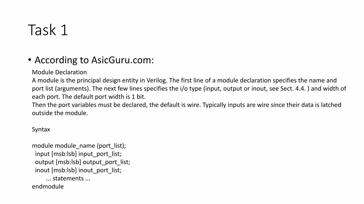
• According to AsicGuru.com:
Module Declaration A module is the principal design entity in Verilog. The first line of a module declaration specifies the name and port list (arguments). The next few lines specifies the i/o type (input, output or inout, see Sect. 4.4. ) and width of each port. The default port width is 1 bit. Then the port variables must be declared, the default is wire. Typically inputs are wire since their data is latched outside the module. Syntax module module_name (port_list); input [msb:lsb] input_port_list; output [msb:lsb] output_port_list; inout [msb:lsb] inout_port_list; ... statements ... endmodule

Task 1
• In our case a module has been defined that has two ports: • The 8 bits wide ld is an output
• The 8 bits wide sw is an input
• Both sw and ld are wires
• Now you have to add statements to the module to define its behavior
• In the first task, we will implement two four-input gates: an AND gate and an OR gate
• The inputs of the AND gate will be the first four switches (from the right). The second 4 switches will be the inputs of the OR gate.

Task 1
• The output of the AND gate will be connected to the rightmost LED, ld[0]. The output of the AND gate will be connected through a NOT gate to ld[1] too.
• The OR gate’s output will be connected to ld[2], and its inverse to ld[3].
• The Boolean equations are the following:
• ld[0] = sw[0]·sw[1]·sw[2]·sw[3], ld[1]=(sw[0]·sw[1] ·sw[2] ·sw[3])’
• ld[2] = sw[4]+sw[5]+sw[6]+sw[7], ld[3]=(sw[4]+sw[5]+sw[6]+sw[7])’

Task 1
• The following operators can be used in Verilog to implement the AND, OR and NOT operations:
Name Verilog operator Example
AND & a&b (2 input AND)
OR | a|b|c (3 input OR)
NOT ~ ~x

Task 1
• Add the following lines to the module
• The above code shows that signals of type wire can be driven continuously using the assign statement.
• You can see that the value assigned to a wire can be a constant or an expression (last line vs lines above).
• We set the upper 4 LEDs to constant 0 otherwise we would receive warning during the implementation

Task 1
• The 4’b0000 expression is a constant. The 4 shows the bit width of the constant, b shows that its given in a binary form, and 0000 is the 4 bit value we want to assign.
• You can also define decimal or hexadecimal constants: • 4’d10: 4-bit decimal constant (1010)
• 5’hB: 5-bit hexadecimal constant (01011)
• The resulting constant is always in binary form, the b, d, h specifiers define the base of the source, not the final result!

Task 1
• Before implementing the design, we are going to test it using the simulator
• Before you do anything, make sure you have saved the modifications
• As a next step, switch to Simulation mode in the top left corner of the ISE:

Task 1
• Right click on the xc3s250e-tq144 label, and select New Source

Task 1
• Select Verilog Test Fixture
• Name: module_1_tf
• Do not modify the Location
• Make sure the “Add to project” checkbox is set
• Press Next

Task 1
• The following windows appears, module_1 should be selected (since we want to test it):
• Press Next, then press Finish

Task 1
• The ISE generates the skeleton for the test fixture file. Go to the initial begin – end part:

Task 1
• Here you can define arbitrary input for the module. The syntax is the following: #T sw = CONSTANT
• T defines the time interval (in nanoseconds) the simulator waits before setting the value defined with CONSTANT on the given variable (sw in this example).
• First, let’s wait 100 nanoseconds, then set the input of the AND gate to 1101 and the input of the OR gate to 1000:
• To do so, add the following line after the Add stimulus here part: #100; sw = 8'b10001101

Task 1
• The input can be interpreted as the following:
• #100; sw = 8'b10001101
• We want to wait 100 ns before setting the value
• The constant is given in binary form, and we want to define an 8-bit value
• The input of the OR gate is 1000, since sw[7], sw[6], sw[5] and sw[4] is the 4 input bits of the OR operation
• The input of the AND gate is 1101, since sw[3], sw[2], sw[1] and sw[0] are connected to the inputs of the AND operation

Task 1
• Add two more lines to the stimulus part:
Before continue, make sure all changes are saved!

Task 1
• Select the module_1_tf file in the top left corner by left clicking on it
• After selecting it, press the + button next to the Isim simulator:

Task 1
• To new options appear: “Behavioral Check Syntax” and “Simulate Behavioral Model”
• Right click on Simulate Behavioral Model, and select “Rerun All”

Task 1
• The simulation output window pops up, you should see something like this:

Task 1
• To see the full result of the simulation, press the “Zoom to full view” button on the bar above the main window.
• To see the output bits one-by-one, click on the triangle next to ld:
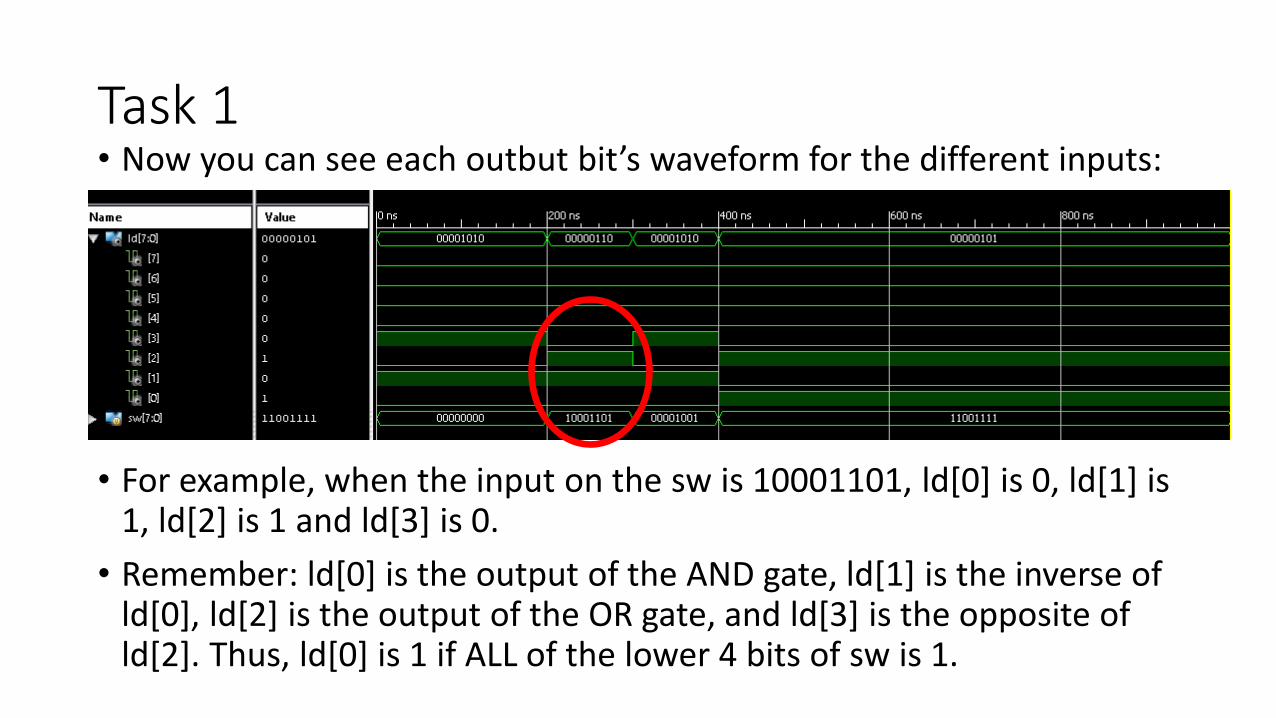
Task 1 • Now you can see each outbut bit’s waveform for the different inputs:
• For example, when the input on the sw is 10001101, ld[0] is 0, ld[1] is 1, ld[2] is 1 and ld[3] is 0.
• Remember: ld[0] is the output of the AND gate, ld[1] is the inverse of ld[0], ld[2] is the output of the OR gate, and ld[3] is the opposite of ld[2]. Thus, ld[0] is 1 if ALL of the lower 4 bits of sw is 1.

Task 1
• Similarly, ld[2] is 1 if ANY of the upper 4 bits of the sw input is 1.
• Check the output for the other input combinations you have set in the test fixture file. Is the result in accordance with your expectations?
Task 1
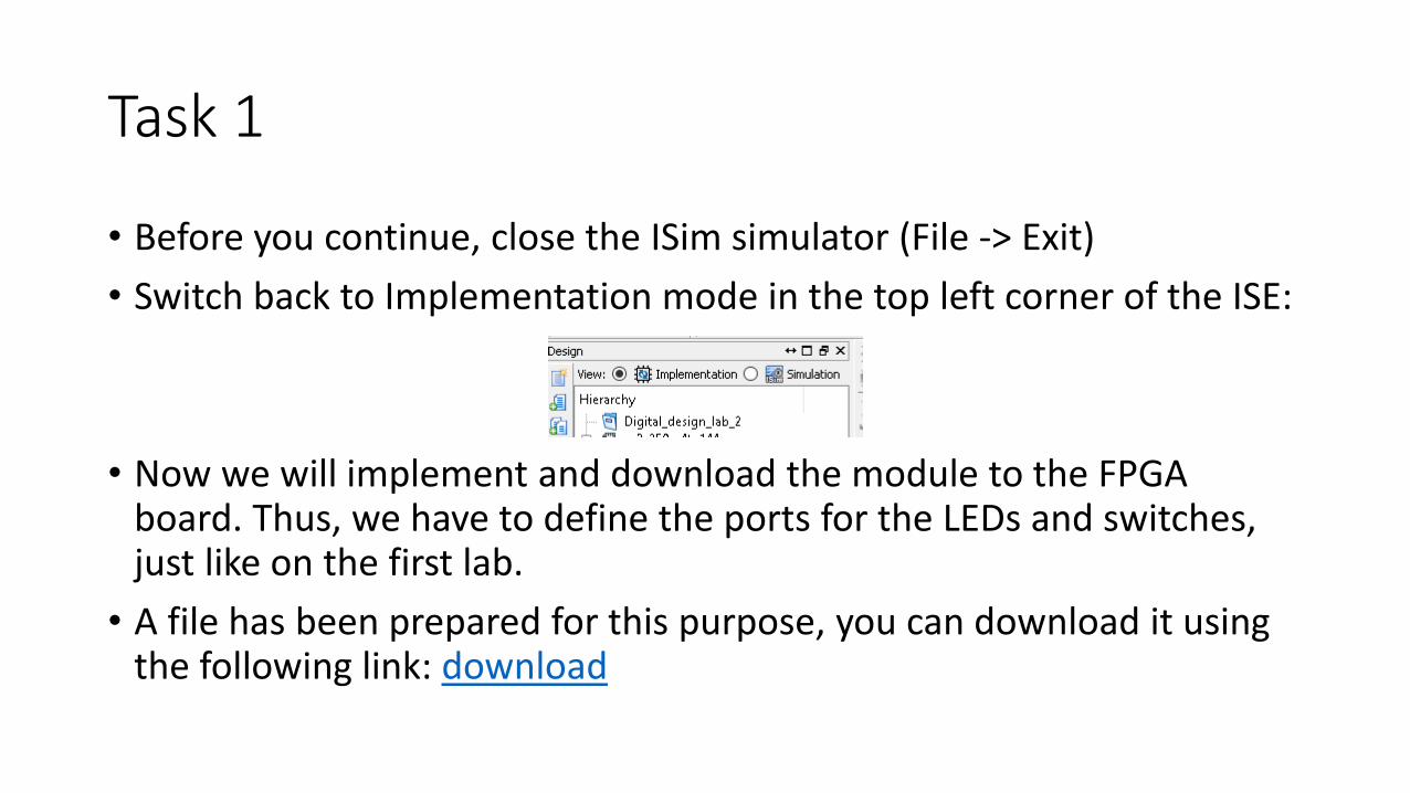
• Before you continue, close the ISim simulator (File -> Exit)
• Switch back to Implementation mode in the top left corner of the ISE:
• Now we will implement and download the module to the FPGA board. Thus, we have to define the ports for the LEDs and switches, just like on the first lab.
• A file has been prepared for this purpose, you can download it using the following link: download
Task 1
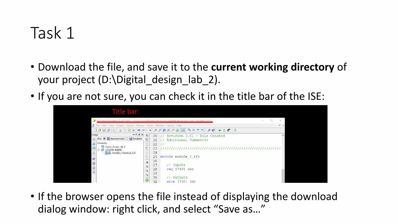
• Download the file, and save it to the current working directory of your project (D:\Digital_design_lab_2).
• If you are not sure, you can check it in the title bar of the ISE:
• If the browser opens the file instead of displaying the download dialog window: right click, and select “Save as…”
Title bar:

Task 1
• After saving the file (with .ucf extension), go back to the ISE, right click on the xc3s250e-4tq144 label, and select “Add Copy of Source…”

Task 1
• Select the downloaded ucf file, and press Open:

Task 1
• The following window appears, press Ok:
Task 1
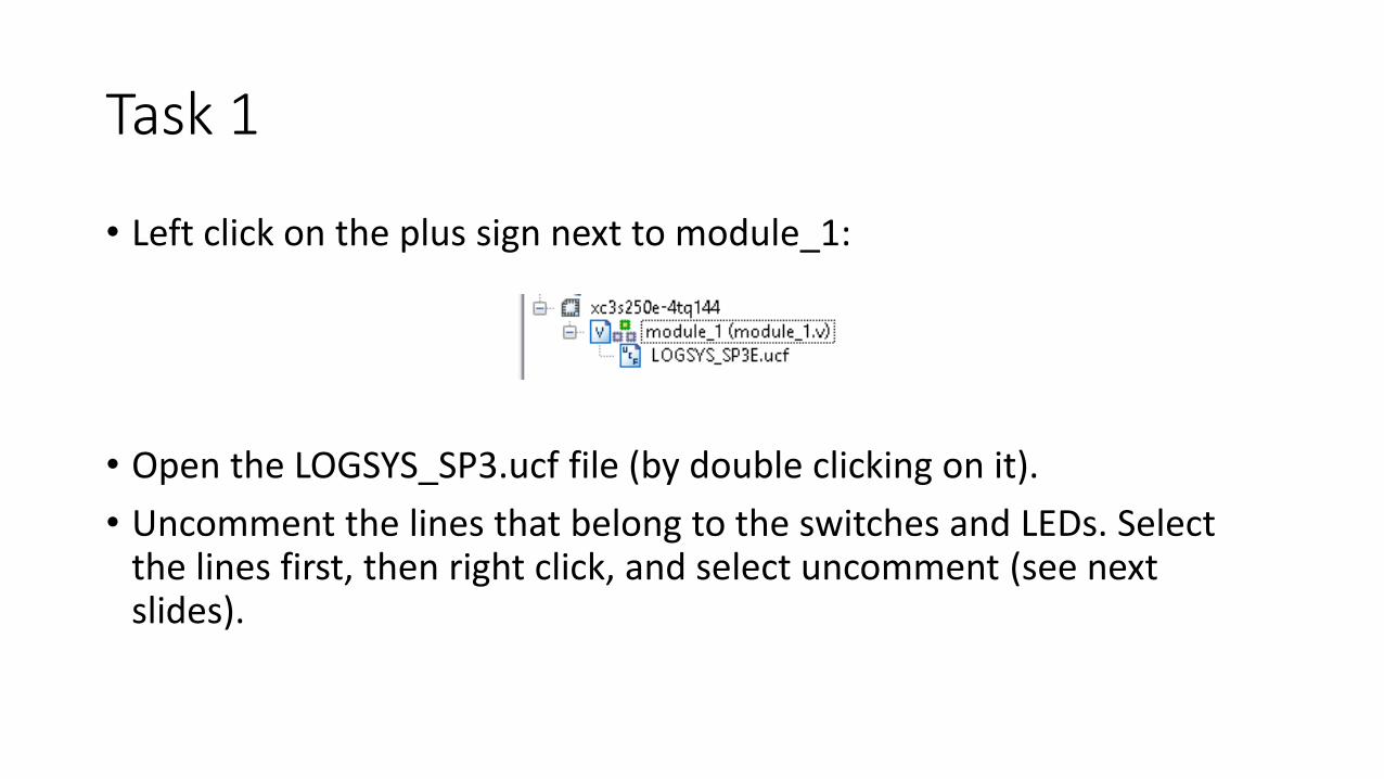
• Left click on the plus sign next to module_1:
• Open the LOGSYS_SP3.ucf file (by double clicking on it).
• Uncomment the lines that belong to the switches and LEDs. Select the lines first, then right click, and select uncomment (see next slides).
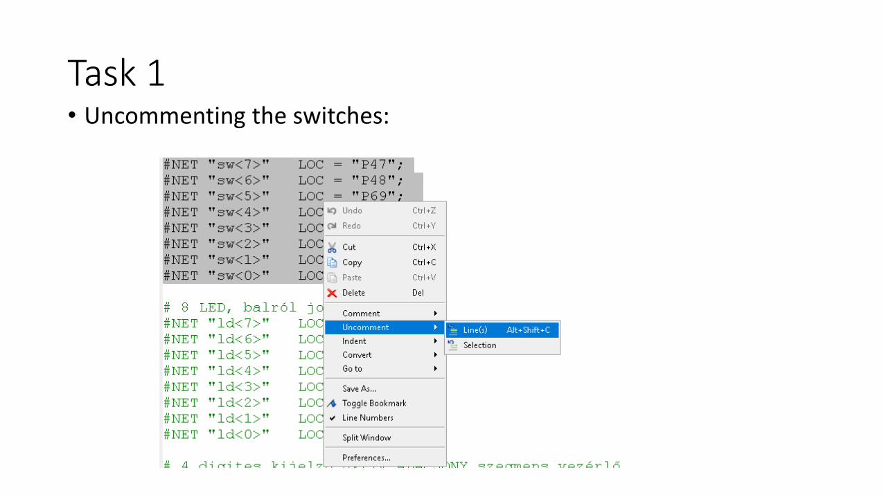
Task 1 • Uncommenting the switches:

Task 1 • Uncommenting the leds:
• Press Save

Task 1
• Select the module_1 file again on the left side:
• On the bottom left side of the screen, double click on “Generate Programming File”
• If everything went fine, you should see this:
Task 1
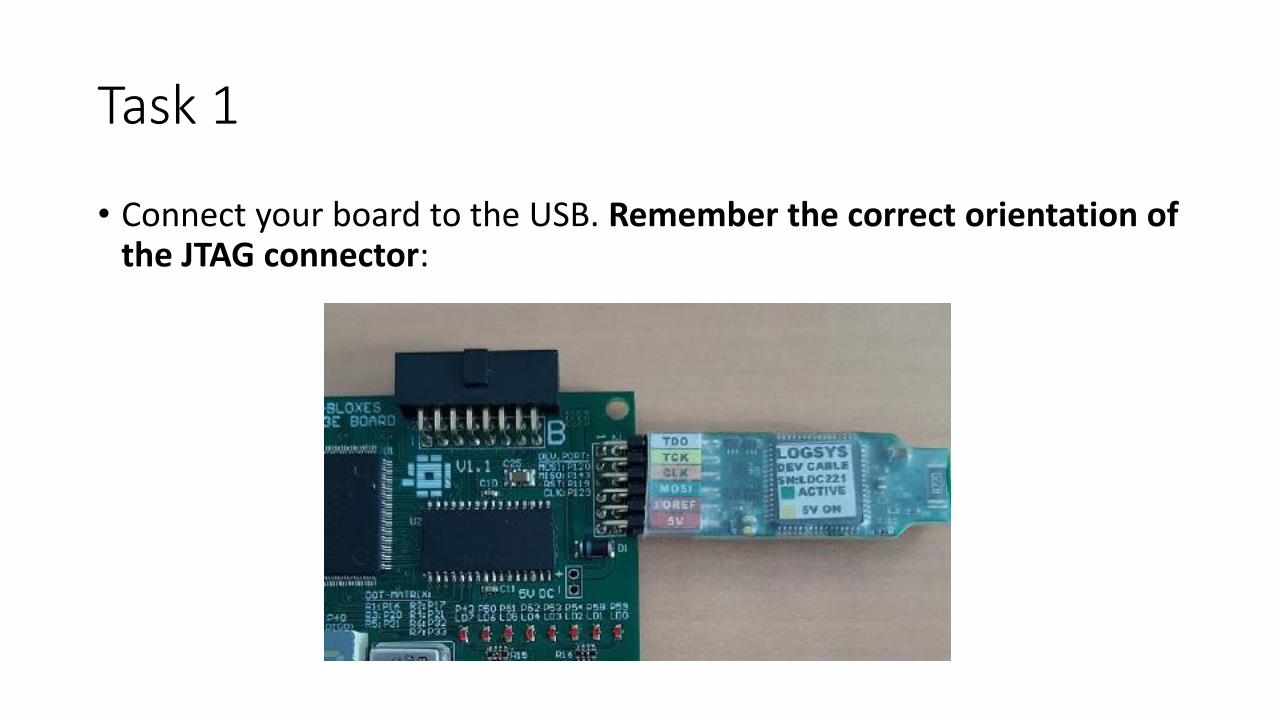
• Connect your board to the USB. Remember the correct orientation of the JTAG connector:

Task 1
• Start the LOGSYS GUI application:
• First, press the Power button:

Task 1
• Press the JTAG Download checkbox:
• Press the Query JTAG chain button:
• Then press the Configure the selected device… button

Task 1
• Browse your working directory and select the generated bitfile, and press Open:

Task 1
• Verify the correct behavior of the network using multiple input combinations. Are the LEDs turning on and off as you expect?

Task 2
• In the next task, we will create a simple combinational circuit that has four inputs: a, b, c, d
• Input a will be driven by sw[3], b by sw[2], c and d by sw[1] and sw[0].
• The four input bits abcd will represent four bit binary numbers from 0 to 15.
• The output of the circuit will indicate whether the input can be divided by 5 or not (the remainder is 0).
• The following numbers fulfills this condition in the 0-15 domain:
• 0, 5, 10, 15
Task 2
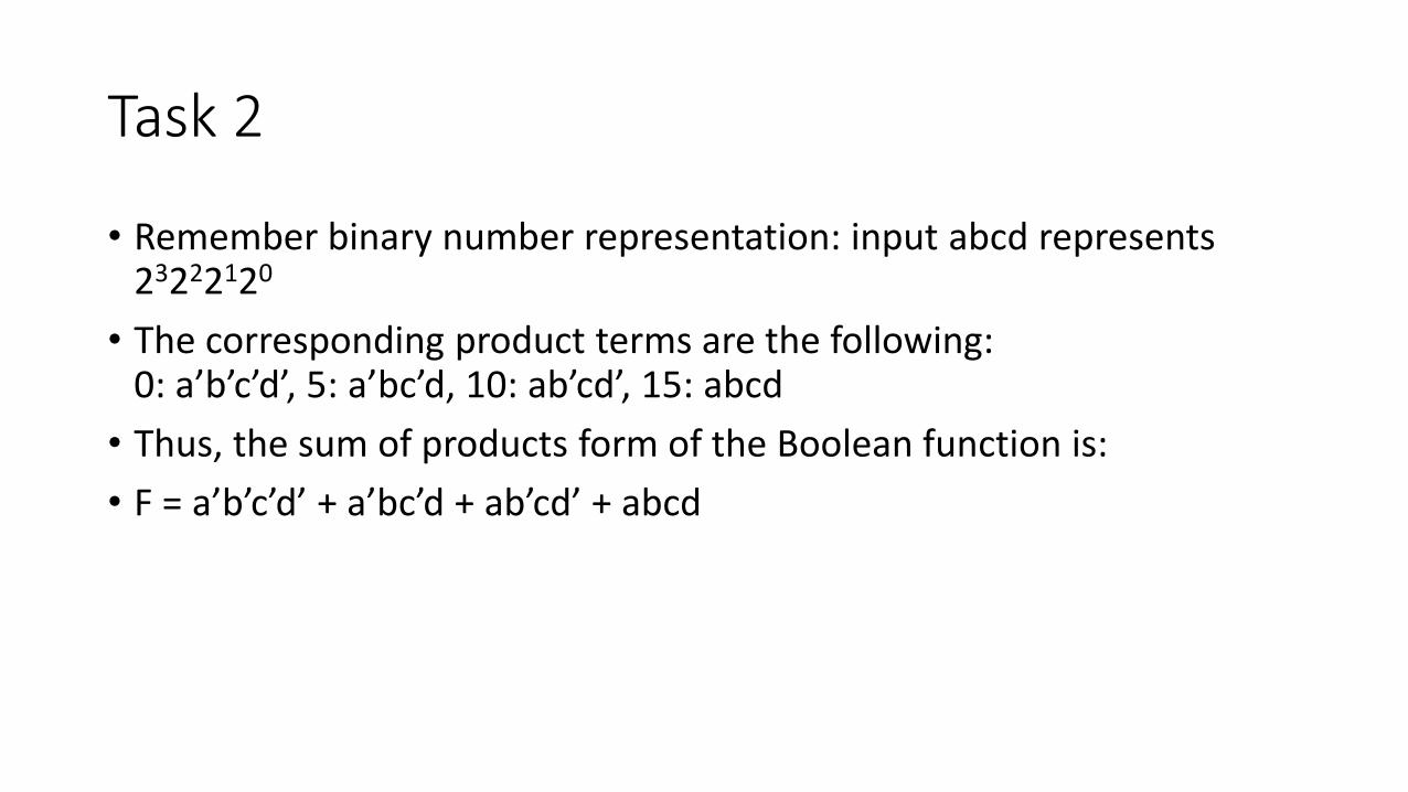
• Remember binary number representation: input abcd represents 23222120
• The corresponding product terms are the following: 0: a’b’c’d’, 5: a’bc’d, 10: ab’cd’, 15: abcd
• Thus, the sum of products form of the Boolean function is:
• F = a’b’c’d’ + a’bc’d + ab’cd’ + abcd

Task 2
• Add a new Verilog module to the project. If you need help, use slides 7-10
• Name: div_5
• Inputs: sw and ld, the same as in Task 1
Task 2
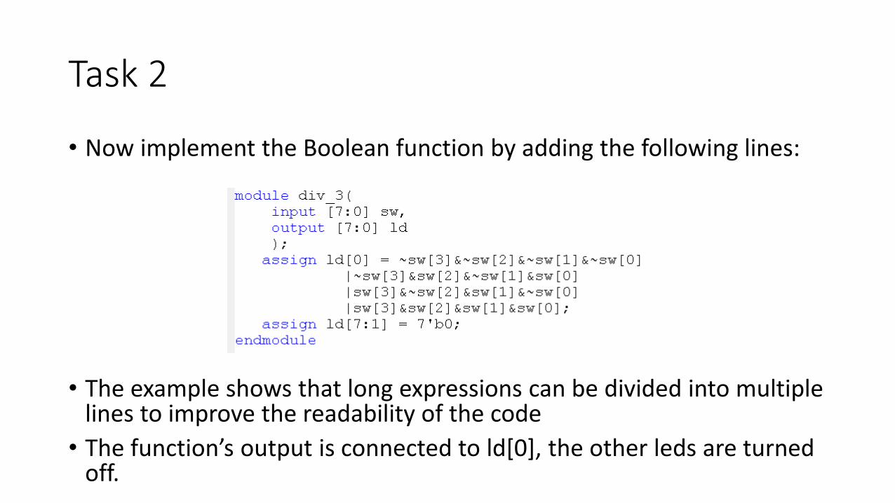
• Now implement the Boolean function by adding the following lines:
• The example shows that long expressions can be divided into multiple lines to improve the readability of the code
• The function’s output is connected to ld[0], the other leds are turned off.

Task 2
• Right click on the div_3 file, and select “Set as Topmodule”

Task 2
• Generate the programming file and upload it to the board. Using the switches, verify the circuit for every input from 0 to 15.
• If you need help, check slides 39-43
• Note: you will get some warnings since sw[7]..sw[4] is not used in this design. You can ignore this right now
• If you still have time: try to implement a function on your own thats output is one if the input can be divided by 3