digital ground bounce reduction by phase modulation … · digital ground bounce reduction by phase...
TRANSCRIPT

Digital Ground Bounce Reduction by Phase Modulation of the Clock
Mustafa Badaroglu1,2, Piet Wambacq1, Geert Van der Plas1, Stéphane Donnay1, Georges Gielen3, and Hugo De Man1,3
1IMEC, Kapeldreef 75, B-3001 Leuven, Belgium, 2Also Ph.D. student at K.U. Leuven, Belgium,
3K.U. Leuven, Belgium
Abstract The digital switching noise that propagates through
the chip substrate to the analog circuitry on the same chip is a major limitation for mixed-signal SoC integration. In synchronous digital systems, digital circuits switch simultaneously on the clock edge, hereby generating a large ground bounce. In order to reduce the spectral peaks in the ground bounce spectrum, we combine the two techniques: (1) phase modulation of the clock and (2) introducing intended clock skews to spread the switching activities. Experimental results show around 16 dB reduction in the spectral peaks of the noise spectrum when these two techniques are combined. These two techniques are believed to be good candidates for the development of methodologies for digital low-noise design techniques in future CMOS technologies.
1. Introduction With the increase of switching speed of digital circuits
and tighter signal-to-noise ratio specifications in analog circuits, ground bounce is a stopper for single-chip integration of mixed-signal systems [1][2]. Even if for a mixed-signal application, the analog part is put on a separate die than the digital part, the data converters are usually put on the same chip as the digital part, where they are subject to noise coupling, which is mainly caused by ground bounce in the digital domain.
A technique called spread spectrum clock generation (SSCG) was introduced in [3] to reduce the spectral peaks of the digital clock as much as 10-20 dB by frequency modulation of the clock with a unique waveform. Through this modulation, the energy at each clock harmonic is distributed over a wider bandwidth. For the case of a 266 MHz clock with a triangular modulation and with a 2.5% frequency deviation, around 13 dB attenuation is measured with this technique [4]. However, the previous work ignores the potential of clock modulation on reducing the ground bounce, which is the subject of this paper. The reduction is not limited to the clock signal only, which is a periodic signal, but it also applies to the supply current, which is not a periodic signal. This non-periodicity, together with the inherent wideband nature of the system supply current makes the analysis
much more difficult on how much reduction can be achieved by the spread spectrum clocking.
This paper presents the two methodologies for ground bounce reduction based on the shaping of the supply current: (1) phase modulation of the system clock in order to reduce the spectral peaks at the discrete harmonics, and (2) introducing intended skews to the synchronous clock network in order to spread the simultaneous switching activities [5]. Previous work has focused more on a single cell with a single-cycle input and ignored the impact of the system-level clocking on the ground bounce [6].
Ground bounce power is proportional to the integral of its spectrum, resulting from the multiplication of the supply current spectrum and its transfer function to the ground node. Since most of the noise power is concentrated around the frequency of the resonance of the package and supply line inductance with the circuit capacitance, reducing the power spectrum in the vicinity of this resonance will also reduce the ground noise [5]. In this paper we derive the system-level clocking conditions in order to achieve a desired level of reduction in the ground noise spectrum at the resonance by choosing the frequency and magnitude of the modulating waveform. The results for a 40 Kgate telecom circuit show a 16 dB reduction in the ground noise spectrum when these supply current shaping techniques are employed.
The paper is organized as follows. Section 2 briefly describes the mechanisms that cause ground bounce. Section 3 presents an analysis to determine the modulating waveform for less ground bounce. Section 4 presents simulation results on the reduction efficiency of the proposed conditions. Finally conclusions are drawn.
2. Supply current and its transfer function to the ground node
Ground bounce can be computed from the product of the spectrum of the supply current source with its transfer function to the ground node (Fig. 1a). This transfer function is derived by using an extracted chip-level ground bounce model [5]. In this model the impedance between Vdd and Vss is represented by a capacitance (Cc) in series with a resistance (Rch) in parallel with a capacitance (Cch) (Fig. 1b). This Vdd-Vss impedance is determined by the junction, channel, well and overlap capacitances. The
1530-1591/04 $20.00 (c) 2004 IEEE

supply line inductance and its series resistance are Lb and Rb, respectively. Additional on-chip decoupling capacitance and its series damping resistance are Cd and Rd, respectively. A designer has the following options to reduce the generated ground bounce:
NNNNfNr
tftr
fr ∈= ,, (3)
Frequency (f)
I(f)
fc
Corner Frequency
Envelope Term
0 Timetr+tftr
Ip
i(t)
OscillatingTerm
(a) (b)
(1) Reducing the supply noise (i(t)) (e.g. by flattening the supply current or reducing the supply voltage),
(2) Changing the transfer function of the supply current source to the ground node (H(s)) (e.g. by increasing the decoupling to reduce the effect of switching capacitance, or by increasing the damping of the oscillations, or by decreasing the supply line inductance).
Fig. 2: Triangular approximation of the supply current in (a) time-domain (b) frequency domain.
-60
-50
-40
-30
-20
-10
0
0 1/T 2/T 3/T
(a) envelope tr = tf = T (b) spectrum tr = tf = T(c) envelope tr = .9T, t f = 1.3T(d) spectrum tr = .9T, t f = 1.3T
Spectrum - [dBA]
Frequency - [Hz]
26.5dBA
(b)
(c)(a)
20log10(E)
(d)
16.7dBA
6.2dBA
.77/T
Supply current I(s)
Supply current transfer function
H(s)
Ground Bounce Vss(s)
Cc
i(t)
Vdd
Lb Lb
Rb RbVdc
Rch
Cd Rd
Vss
(a)
Cch
(b)
Fig. 1: (a) Block level model of ground bounce generation. (b)
Chip-level ground bounce model. Fig. 3: The spectrum of the triangular supply current.
2.1. Supply current spectrum Fig. 3 shows the spectrum and the envelope for a
supply current waveform with tr and tf equal to T. This waveform has a notch point at the frequency 1/T. Since the envelope is given by 2.Ip.(tr+tf)/(ω2.T2), the second lobe has a 26.5 dB smaller amplitude than the DC point. While an incremental change in tr and/or tf can shift the notch point to higher frequencies, a main lobe remains present. In addition to the attenuation due to the fact that the envelope is a decreasing function of frequency, at fc the “oscillating” term provides an extra attenuation with a factor sin(α.π)/(1+α), with α equal to min(tr,tf)/max(tr,tf). As an example (Fig. 3), for tr and tf equal to 0.9T and 1.3T, respectively, fc becomes 0.77/T. At that point, the total attenuation of 22.9 dB consists of an envelope attenuation of 16.7 dBA and an extra attenuation of 6.2 dBA while the notch point occurs at 10/T.
For synchronous CMOS circuits, the total supply current in the time domain can be approximated by a periodic triangular waveform. To better understand the properties of this waveform, we first study a single-cycle triangular waveform (Fig. 2a). In the next section we will extend to the multiple-cycle case. The Fourier transform of this single-cycle waveform is in fact the envelope of the multiple-cycle waveform. The single-cycle waveform can be characterized by Ip, tr, and tf, which are the peak current, rise time, and fall time respectively. The supply current can be written as a function of the four ramp signals:
( )
( )
−−−−
+−−=
)()(.1
)()(.1
.)(trtrtrtftr
tf
trtrtrtrIpti
(1)
where r(t) is the unit ramp function. The Fourier transform of the supply current i(t) is given by (Fig. 2b):
( ) ( )
( )( )2
2
2
......2
)).cos(1.()).cos(1.(
).sin(.).sin(...
)(
.1111)(
)(
tftrtrtf
tftrtrtftftrIpI
eetf
etrj
IpI trjtfwjtrwj
ωω
ωωω
ω
ωω ω
−+−
+−=
−+−= −−
(2)
The power spectrum of the supply current can be reduced by increasing tr, tf, and/or by decreasing Ip. This can be done by introducing different skews to the branches of a clock tree driving a synchronous digital circuit. This skew is realized by splitting the design into several clock regions and introducing skews for each clock region and to finally implement a clock delay line, which generates a separate clock for every clock region [5].
Although the supply current is not a purely periodic signal, it will be shown in Section 2.3 that the spectrum of the supply current closely resembles to the spectrum that results from the periodic repetition of the single-cycle triangular waveform that has been computed as the average over all cycles, further referred to as the ensemble average of the supply current. Decreasing the operating
From Fig. 2b we see that this spectrum shows a first local minimum at a frequency fc. From eqn. (2) we find that fc corresponds to the minimum of 1/tr and 1/tf. Here, fc is the so-called corner frequency of the supply current. The first local minimum can even be a notch (i.e. I(ω)=0) when tr=tf. In fact the notch points satisfy:

frequency of the circuit will increase the number of harmonics and thus the number of envelope points visible. This is demonstrated in Fig. 4, which compares the spectrum of the ensemble average of the supply current to the spectrum of the actual SPICE-simulated supply current of a 100 gates circuit for a period of 3 ns (top) and 30 ns (bottom). This indicates that the spectrum of the ensemble average of the supply current matches that of the actual current transient at the clock harmonics.
-40
-20
0
-40
-20
0
0 500 1000 1500 2000 2500 3000 3500 4000
~
Frequency - [Mhz]
Supply Current Spectrum - [dBA]
Supply Current Profile
T = 3ns
T = 30ns
with padded zeros
Fig. 4: The spectra of the total supply current and the
ensemble averaged supply current of a 100 gates circuit for a period of 3 ns (top) and 30 ns (bottom).
The discrete spectrum is determined entirely by the average behavior of the digital switching current pulses in a synchronous digital system. The cycle-to-cycle variations of the supply current cause a (non-constant) noise floor to the spectrum, as seen in Fig. 4. The next section will explore by how much the energy of the discrete spectrum of the power supply current, that follows the spectrum of the ensemble average, exceeds the energy of this noise floor. The distance in dB between the discrete spectral lines and the noise floor around the spectral line under consideration will correspond to the maximum reduction of the energy in that spectral line by modulation of the clock as will be discussed in Section 3. 2.2. Supply current cycle-to-cycle variations
The comparison of the rms value of the ensemble average of the supply current (iavg(t)) to the variations (n(t)) of the supply current around its average value will give the ratio η between the total energy of the spectral peaks and the total energy of the noise floor [7]:
dffPdffP dm .)(/).(00∫∫∞∞
=η (4)
where Pd(f) and Pm(f) are the power spectral densities (psd) of the cross-covariance function and the ensemble average of the supply current respectively. The cross-covariance component arises from the cycle-to-cycle variations of the supply current. We define kp, kr, and kf as the maximum relative variations of the peak value, rise time, and fall time of the supply current, respectively,
normalized to their mean values. The autocorrelation of the ensemble average is a periodic pulse train consisting of the waveforms with the peak values given by the average power of a single cycle and with a pulsewidth equal to two times the pulsewidth of the supply current. The average signal power of the ensemble average equals Ip2.(tr+tf)/(3.Tclk). For a uniformly distributed variation, which is defined as an additive noise on the average supply current, the average variation power equals kp2.Ip2/3 where kp.Ip is the maximum allowed variation of the additive noise. The comparison of the signal powers of the average current and the additive noise yields η2=(tr+tf)/(kp2.Tclk).
(a)
(b)
0
0.5
1
-0.5, 1.5
0
0.5
1
0 10 20 30 40 50 60 70 80
Supply current i(t)=iavg(t)+n(t)[A]
Time - [ns]
iavg(t)
n(t)
i(t)
-70
-60
-50
-40
-30
-20
-10
0
0 5 10 15 20 25 30
[dBA] Frequency spectrum of i(t)=iavg(t)+n(t)
nth harmonic of the clock
Iavg(f)
N(f)
I(f)
Fig. 5: (a) Supply current waveform i(t)=iavg(t)+n(t) when
kp=0.5, kr=0.2, and kf=0.5 (b) Corresponding spectral power at each harmonic bin of the clock.
In reality the supply current variation is not additive. A more realistic case occurs when the parameters Ip, tr, and tf change randomly. When these change independently and with a uniform distribution then η is given by:
9/.3/3/( 2222 krfkpkrfkp ++=η (5)
where krf is defined as the percentage variation of the pulsewidth of the supply current, which is given by krf=(kr.tr+kf.tf)/(tr+tf).
To illustrate the above analysis we consider a fictitious current waveform with 1 A peak value, 1 ns rise time, 5 ns fall time, and 10 ns clock period. The peak value (Ip), rise time, and fall time of the supply current are changed uniformly with ±0.5 A, ±0.2 ns, and ±2.5 ns, respectively (Fig. 5a). These variations are artificially large just for the sake of illustration. The corresponding spectrum of the average supply current and its variation are shown in Fig. 5b. η is computed as 8.15 dB after computing the total spectral power of iavg(t) and n(t) by using the simulation

data while the estimation for η with eqn. (5) is 8.06 dB. A variation in the rise/fall time makes the notches to disappear, but this is not relevant since these notches occur(red) at higher frequencies where the power spectral density is already very low.
Any reduction technique that uses the periodicity of the average supply current, has a margin of 2η (in dB) to reduce the power spectral density of the supply current. This will be exploited in section 3. However, the energy of the supply current is also decreased due to the fact that this spectrum is multiplied by the transfer function from the supply current to the ground node, which has a bandpass characteristic, as will be explained in section 2.3.
From this section, we conclude that rather than using the actual supply current it is sufficient to use the ensemble average supply current as a periodic pulse for the representation of the supply current with an error bound η (eqn. (5)). 2.3. Supply current transfer function to the
ground node By using the model of Fig. 1b the voltage swing at the
Vss node is computed with the supply current as the input after converting the network to an equivalent parallel RLC-network. The capacitance (CP) and inductance (LP) of this parallel RLC-network are given by:
LbLbRbLP=
)CdRd+(Cd
CchCcRch+CcCchCcCchRchCcCP=
.)..(2
1).(.1)..(..
2
222
222222
22
ωω
ωωω
+
++++
(6)
The resonance frequency (fo) is given by:
CPLPfo ..2
1π
= (7)
In order to solve eqn. (7), an iterative approach can be employed by first finding an initial value of fo for LP=2.Lb and CP=Cc+Cd. This fo is then used in order to update the new values of LP and CP.
Cc [fF]
Rch [Ω]
Cch [fF]
Area [NAND2]
B01 912-1041 6.1038-5.5070 349-512 110 B02 846-961 11.649-10.612 239-369 95 B03 5261-6008 2.1309-1.9485 1455-2306 604 B04 15754-17911 0.74069-0.67836 4459-6947 1776 B05 11431-13000 0.47179-0.42399 4782-6909 1319 B17 279565-320435 0.01732-0.01554 132949-190750 39782 B18 748855-862358 0.00679-0.00610 360566-523212 102326 B20 144732-167026 0.03940-0.03548 69357-102309 18638 B21 71784-82895 0.07980-0.07185 34653-51225 9366 B22 134384-155622 0.04065-0.03659 67923-100129 17839
Table 1: Ground bounce macromodel parameters without/with the local interconnect effects for ITC'99 benchmark circuits (leftmost column) synthesized in a 0.18 µm CMOS process.
Table 1 lists the extracted ground bounce macromodel parameters for ITC’99 benchmark circuits [8] with and without the local interconnect effects (interconnect only within the gate and no signaling interconnect between the
gates). The accuracy of the ground bounce macromodel parameters has been verified with measurements [9]. The data show that ignoring the interconnect overestimates the resonance frequency with about 5-6%. This overestimation increases up to 15% when the signaling between the gates is also taken into account [9]. An accurate estimation of the resonance is important for the efficient implementation of the phase modulation of the system clock as well as of the intended clock skews.
3. Phase modulation of the system clock and its impact on the supply current
Phase modulation of the clock will reduce the harmonics in the discrete spectrum by creating sidelobes around the clock harmonics. This will decrease the energy of the discrete spectrum, which was shown in Section 2.2 to be the dominant component of the supply current. In the time domain this leads to a supply current with a different phase at each cycle. This supply current i(k) is monitored (k represents the discrete time) over a time interval of R clock cycles, and each cycle consists of K time samples:
∑−
=
−−=1
0))(.()(
R
rr rdKrkiki (8)
where the current pulse ir(k) in each period is a stochastic variable and each clock cycle r is a trial whose outcome is ir(k). Further, ir(k) is zero outside the interval 0<k<K. The parameter r selects a clock cycle (r: 0→R-1) and d(r) is the phase introduced in clock cycle r. The discrete-time Fourier transform (DFT) of this supply current is given by:
( )∑∑−
=
−
=
−−−=1
0
1
0
../2.)).(.()(K
k
R
r
lkRKjr erdKrkilI π (9)
After expanding the DFT of eqn. (9) for each cycle r the DFT at point l=p.R (at the p-th harmonic of the system clock) for the single cycle is given by:
Re
eepW
pWpIRplI
pRdKj
pdKjpdKj
r
/....
)(
)().().(
).1()./2.(
).1()./2.().0()./2.(
+
++=
==
−π
ππ
(10)
where Ir(p) is the DFT of the single cycle when the supply current is periodic with the K data points, i.e. ir(k-r.K)= ir(k) at each clock cycle r. In the case when d(r) is zero for all R values, the DFT of the supply current is equal to the DFT of a single cycle. d(r) can be chosen as either a cyclic pseudo random sequence or a periodic triangular waveform. We define m as the number of clock cycles for the modulating waveform d(r) to complete its one period. In order to achieve a significant reduction at the p-th harmonic, the amplitude of the variation in the time-domain should be chosen as:
pKrd /))(max( = (11)

With this choice on the amplitude of the variation W(p) always evaluates to zero for both triangular and pseudo random waveforms. For a significant reduction p is chosen as the harmonic at the circuit resonance fo given by eqn. (7). Then we have:
TclkfKrd
o .))(max( = (12)
where Tclk is the clock period. Fig. 6 shows the frequency spectrum of the different modulating waveforms: triangular, pseudo random, and square for m=16 and max(d(r))=0.2. It is clearly seen that a triangular modulating waveform is among the best when the supply current bandwidth is limited to the first 20 harmonics of the clock. At the 5th harmonic W(p) evaluates to zero as also given by eqn. (11). The reduction at the discrete clock harmonic will be very significant if the resonance is centered at the 5th harmonic of the system clock. On the other hand, this reduced energy at this harmonic is spread onto the sideband harmonics. Other modulation profiles exist, which give more suppression in these sideband harmonics, such as the nonlinear SSCG waveform (Hershey Kiss Profile) [3]. However this profile suffers from its hardware implementation.
-20
-10
0
-30
-20
-10
0
-30-20
-10
0
0 10 20 30 40 50 60 70 80 90 100pth harmonic of the clock
[dB]TriangularWaveform
PseudoWaveform
SquareWaveform
Fig. 6: Frequency spectrum of the different modulating waveforms: Triangular, Pseudo Random, and Square.
An important constraint for a digital system is to have a small cycle-to-cycle jitter in order to avoid setup time violations. The periodic triangular waveform has shown to be the best choice to have a minimum jitter. In this case the cycle-to-cycle jitter ∆kc is limited to:
mpKkc..2
=∆ (13)
m determines the periodicity of the function W(p) in the frequency domain as given by eqn. (10). A minimum value of m should be chosen such that the bandwidth of the supply current, BW(Ir(p)), is less than the spectrum periodic frequency of the modulating waveform W(p).
ppIrBWTclkm ))((..4
> (14)
The bandwidth of the supply current is defined by max(1/tr,1/tf) where the supply current has a notch in the
case when tr and tf are integer multiples of each other. On the other hand m should not be chosen too large since this will result into a too small unit delay ∆kc (eqn. (13)), which cannot be realized in practice.
Phase modulation of the clock can be constructed easily with a multiplexer choosing the multiphase outputs of the clock source.
4. Experimental Results The proposed methodology is illustrated with the two
examples: two maximum-length 10-bit Pseudo-Random-Binary-Sequencers (PRBS) with a correlator, and a large telecom circuit (40 Kgate), both implemented in a 0.18 µm 1.8 V CMOS process.
10-bit PRBS
10-bit PRBS
EnbL
EnbR
ClkP
10-bit XOR logic
Ones Count Logic Ones[3:0]
10
10
10
Macromodel Parameters Lb=1 nH Rb=0.1 Ω Cc=9.55 pF Rch=3.11 Ω Cch=2.93 pF
Clk
MultiplexorTriangle
Waveform Generator
m/2 delay units Incrementer (0 to m/2-1)
Decrementer (0 to m/2-1) Unit delay=2.Tclk/p/m=20 ps
Tclk=10 nsm=100
p=5
TEST CIRCUIT
CLOCK SPREADING CIRCUIT Fig. 7: Pseudo-Random-Noise-Sequencer (PRBS) circuits with
the correlator and the clock modulating circuit.
Fig. 7 depicts the two PRBS circuits and the correlator together with the circuit used to modulate the phase of the clock. The figure also shows the macromodel element values and the parameters of the clock modulating circuit. The design has a 100 MHz clock and supply line parasitics of 1 nH + 0.1 Ω. The supply current transfer function to the ground node has a resonance frequency at 1.15 GHz. An ensemble averaged supply current profile has been constructed using the actual supply current data of 1000 clock cycles, which was obtained from SPICE simulations. Choosing 1000 clock cycles, considering the intrinsic periodicity of the 10-bit PRBS, results in an unbiased estimate. The multiplication of the spectrum of the ensemble averaged supply current with the transfer function to the digital Vss node gives the maximum peaking at 1 GHz. Therefore we choose the 10th harmonic (p=10) as the notch of the modulating waveform. As a result of this notch the harmonic at 1 GHz is completely attenuated. The largest sideband harmonic around 1 GHz after phase modulation is 8 dB below with respect to the harmonic at 1 GHz before the phase simulation (Fig. 8).
We have tested the combined impact of the clock phase modulation and intended clock skew in a large telecom circuit consisting of 40 Kgates. The design has a clock period of 20 ns and supply line parasitics of 250 pH + 0.025 Ω. For this circuit, we compute Cc=278 pF, Rch=0.028 Ω, and Cch=159 pF. The design consists of four clock regions where the skew of each
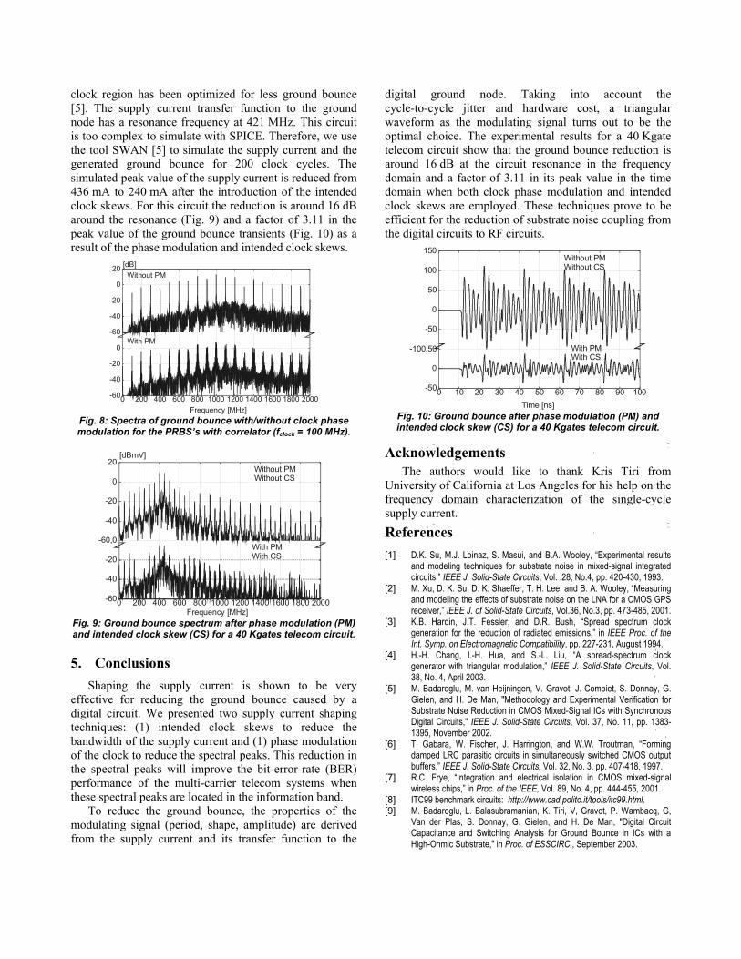
clock region has been optimized for less ground bounce [5]. The supply current transfer function to the ground node has a resonance frequency at 421 MHz. This circuit is too complex to simulate with SPICE. Therefore, we use the tool SWAN [5] to simulate the supply current and the generated ground bounce for 200 clock cycles. The simulated peak value of the supply current is reduced from 436 mA to 240 mA after the introduction of the intended clock skews. For this circuit the reduction is around 16 dB around the resonance (Fig. 9) and a factor of 3.11 in the peak value of the ground bounce transients (Fig. 10) as a result of the phase modulation and intended clock skews.
-60
-40
-20
0
-60
-40
-20
0
20
0 200 400 600 800 1000 1200 1400 1600 1800 2000Frequency [MHz]
[dB]Without PM
With PM
Fig. 8: Spectra of ground bounce with/without clock phase modulation for the PRBS’s with correlator (fclock = 100 MHz).
-60
-40
-20
-60,0
-40
-20
0
20
0 200 400 600 800 1000 1200 1400 1600 1800 2000Frequency [MHz]
Without PMWithout CS
With PMWith CS
[dBmV]
Fig. 9: Ground bounce spectrum after phase modulation (PM) and intended clock skew (CS) for a 40 Kgates telecom circuit.
5. Conclusions Shaping the supply current is shown to be very
effective for reducing the ground bounce caused by a digital circuit. We presented two supply current shaping techniques: (1) intended clock skews to reduce the bandwidth of the supply current and (1) phase modulation of the clock to reduce the spectral peaks. This reduction in the spectral peaks will improve the bit-error-rate (BER) performance of the multi-carrier telecom systems when these spectral peaks are located in the information band.
To reduce the ground bounce, the properties of the modulating signal (period, shape, amplitude) are derived from the supply current and its transfer function to the
digital ground node. Taking into account the cycle-to-cycle jitter and hardware cost, a triangular waveform as the modulating signal turns out to be the optimal choice. The experimental results for a 40 Kgate telecom circuit show that the ground bounce reduction is around 16 dB at the circuit resonance in the frequency domain and a factor of 3.11 in its peak value in the time domain when both clock phase modulation and intended clock skews are employed. These techniques prove to be efficient for the reduction of substrate noise coupling from the digital circuits to RF circuits.
-50
0
-100,50
-50
0
50
100
150
0 10 20 30 40 50 60 70 80 90 100
Without PMWithout CS
With PMWith CS
Time [ns] Fig. 10: Ground bounce after phase modulation (PM) and intended clock skew (CS) for a 40 Kgates telecom circuit.
Acknowledgements The authors would like to thank Kris Tiri from
University of California at Los Angeles for his help on the frequency domain characterization of the single-cycle supply current.
References
[1] D.K. Su, M.J. Loinaz, S. Masui, and B.A. Wooley, “Experimental results and modeling techniques for substrate noise in mixed-signal integrated circuits,” IEEE J. Solid-State Circuits, Vol. .28, No.4, pp. 420-430, 1993.
[2] M. Xu, D. K. Su, D. K. Shaeffer, T. H. Lee, and B. A. Wooley, “Measuring and modeling the effects of substrate noise on the LNA for a CMOS GPS receiver,” IEEE J. of Solid-State Circuits, Vol.36, No.3, pp. 473-485, 2001.
[3] K.B. Hardin, J.T. Fessler, and D.R. Bush, “Spread spectrum clock generation for the reduction of radiated emissions,” in IEEE Proc. of the Int. Symp. on Electromagnetic Compatibility, pp. 227-231, August 1994.
[4] H.-H. Chang, I.-H. Hua, and S.-L. Liu, “A spread-spectrum clock generator with triangular modulation,” IEEE J. Solid-State Circuits, Vol. 38, No. 4, April 2003.
[5] M. Badaroglu, M. van Heijningen, V. Gravot, J. Compiet, S. Donnay, G. Gielen, and H. De Man, "Methodology and Experimental Verification for Substrate Noise Reduction in CMOS Mixed-Signal ICs with Synchronous Digital Circuits," IEEE J. Solid-State Circuits, Vol. 37, No. 11, pp. 1383-1395, November 2002.
[6] T. Gabara, W. Fischer, J. Harrington, and W.W. Troutman, “Forming damped LRC parasitic circuits in simultaneously switched CMOS output buffers,” IEEE J. Solid-State Circuits, Vol. 32, No. 3, pp. 407-418, 1997.
[7] R.C. Frye, “Integration and electrical isolation in CMOS mixed-signal wireless chips,” in Proc. of the IEEE, Vol. 89, No. 4, pp. 444-455, 2001.
[8] ITC99 benchmark circuits: http://www.cad.polito.it/tools/itc99.html. [9] M. Badaroglu, L. Balasubramanian, K. Tiri, V, Gravot, P. Wambacq, G,
Van der Plas, S. Donnay, G. Gielen, and H. De Man, "Digital Circuit Capacitance and Switching Analysis for Ground Bounce in ICs with a High-Ohmic Substrate," in Proc. of ESSCIRC., September 2003.