digital pulse-width modulation control in power electronic
TRANSCRIPT

Digital Pulse-Width Modulation Control in Power Electronic Circuits:Theory and Applications
by
Angel V. Peterchev
A.B. (Harvard University) 1999M.S. (University of California, Berkeley) 2002
A dissertation submitted in partial satisfaction of the
requirements for the degree of
Doctor of Philosophy
in
Engineering-Electrical Engineeringand Computer Sciences
in the
GRADUATE DIVISION
of the
UNIVERSITY OF CALIFORNIA, BERKELEY
Committee in charge:Professor Seth R. Sanders, Chair
Professor Jan M. RabaeyProfessor Kameshwar Poolla
Spring 2005
The dissertation of Angel V. Peterchev is approved:
Chair Date
Date
Date
University of California, Berkeley
Spring 2005

Digital Pulse-Width Modulation Control in Power Electronic Circuits:
Theory and Applications
Copyright 2005
by
Angel V. Peterchev

1
Abstract
Digital Pulse-Width Modulation Control in Power Electronic Circuits: Theory and
Applications
by
Angel V. Peterchev
Doctor of Philosophy in Engineering-Electrical Engineering
and Computer Sciences
University of California, Berkeley
Professor Seth R. Sanders, Chair
This thesis develops digital pulse-width-modulation (DPWM) control of switching
power converters. A target application is microprocessor voltage regulation which requires
high efficiency and tight output load-line control. A general framework for load-line control
is developed, which encompasses different capacitor technologies, such as electrolytics and
ceramics. It is shown that load-current feedforward can overcome the limited bandwidth of
conventional feedback load-line control. The size of the output capacitor is then determined
solely by transient and switching-ripple considerations, which are derived. This work enables
microprocessor voltage-regulator implementations using a small number of ceramic output
capacitors, while running at sub-megahertz switching frequencies.
Efficient DPWM controller implementations are discussed, addressing system sta-

2
bility issues unique to digital control. The existence of limit cycles is analyzed, as well as
conditions for their elimination. Digital dither is introduced as a method to increase the ef-
fective DPWM resolution, thus preventing limit cycling, and enabling low-power, small-area
DPWM implementations.
A method for direct control of synchronous rectifiers as a function of the load
current is developed. The function relating the synchronous-rectifier timing to the load
current is optimized on-line with a perturbation-based power-loss-minimizing algorithm.
This approach provides fast synchronous-rectifier adjustment, robustness to disturbances,
and the capability to simultaneously optimize multiple parameters. It also accomplishes
an automatic, optimal transition to discontinuous-conduction mode at light loads, thus
improving converter efficiency. Efficiency is further enhanced by imposing a minimum
duty-ratio limit to effect pulse-skipping at very light loads.
Three experimental buck converters are developed to illustrate different aspects of
this work. Simulations are used to further corroborate the results.
Professor Seth R. SandersDissertation Committee Chair

i
In memory of my grandparents Bistra and Andrey,
to my mother Antonina,
with love and gratitude.

ii
Acknowledgments
First and foremost, I thank my advisor Professor Seth Sanders for his patient
guidance. Besides his outstanding expertise in both theoretical and practical matter, his
amicable disposition and accessibility have provided for a constructive, yet remarkably
stress-free, collaboration. I believe over these past years I have absorbed some of his no-
nonsense approach to research. He has taught me how to structure my ideas more rigorously,
and I have certainly developed a distaste for ad-hoc solutions in my or other people’s work.
Along with Professor Sanders, I would like to thank Professors Jan Rabaey, Bern-
hard Boser, and Kameshwar Poolla for serving on my qualifying exam committee, and for
asking questions which have periodically resurfaced in my mind and conduced me to sharper
thinking. I also thank Professors Sanders, Rabaey, and Poolla for reading this thesis.
I am greatly indebted to my undergraduate mentors Mr. Winfield Hill, Professor
Jene Golovchenko, and Dr. Steven Saar at Harvard, who have provided continual support.
In addition to teaching me a lot about science and engineering, they have been models of
professional integrity, generosity, and dedication to research. Further, I am grateful to my
high school teachers who, by delivering liberal yet rigorous education, have marshalled my
intellectual maturation and prepared me to compete on the international arena.
My former and present colleagues in the Power Electronics Group deserve a special
acknowledgement for all the miscellaneous chats and sometimes very concrete help: Jinwen
Xiao, Perry Tsao, Matt Senesky, Kenny Zhang, Artin Der Minassians, Gabe Eirea, Jason
Stauth, Mike Seeman, and Yi Zhang. In addition, I thank Jinwen and Kenny for the
successful research collaboration.

iii
Finally, grateful regards go to all my friends in Berkeley and beyond who have
kept me afloat through grad school.
Last but not least, the work toward this thesis was financially supported by the
National Science Foundation, the California Micro Program, Linear Technology, Fairchild
Semiconductor, and National Semiconductor.

iv
Contents
List of Figures vi
List of Tables viii
1 Introduction 11.1 Power Management Challenges of Digital Processing IC’s . . . . . . . . . . 11.2 Potential of Digital Power Management Controllers . . . . . . . . . . . . . . 71.3 Thesis Overview . . . . . . . . . . . . . . . . . . . . . . . . . . . . . . . . . 13
2 Voltage-Regulator Output-Impedance Control with Load-Current Feed-forward 162.1 Introduction . . . . . . . . . . . . . . . . . . . . . . . . . . . . . . . . . . . . 162.2 Output-Impedance Regulation . . . . . . . . . . . . . . . . . . . . . . . . . 202.3 Feedback Control Approaches and Their Limitations . . . . . . . . . . . . . 23
2.3.1 Switching Stability Constraint . . . . . . . . . . . . . . . . . . . . . 232.3.2 Load-Line Feedback . . . . . . . . . . . . . . . . . . . . . . . . . . . 242.3.3 Voltage Feedback with Finite DC Gain . . . . . . . . . . . . . . . . . 26
2.4 Load-Current Feedforward Control . . . . . . . . . . . . . . . . . . . . . . . 292.4.1 Voltage-Mode Control . . . . . . . . . . . . . . . . . . . . . . . . . . 302.4.2 Current-Mode Control . . . . . . . . . . . . . . . . . . . . . . . . . . 32
2.5 Large-Signal Considerations: Critical Capacitance . . . . . . . . . . . . . . 332.5.1 Critical Capacitance Derivation . . . . . . . . . . . . . . . . . . . . . 34
2.6 Switching Ripple Considerations . . . . . . . . . . . . . . . . . . . . . . . . 392.7 Application to Microprocessor Voltage Regulators . . . . . . . . . . . . . . . 40
2.7.1 Design for Low-Conversion Ratio . . . . . . . . . . . . . . . . . . . . 402.7.2 Output Capacitor Size . . . . . . . . . . . . . . . . . . . . . . . . . . 422.7.3 Load-Current Estimation . . . . . . . . . . . . . . . . . . . . . . . . 442.7.4 PWM Modulator . . . . . . . . . . . . . . . . . . . . . . . . . . . . . 462.7.5 Dynamic Reference Voltage . . . . . . . . . . . . . . . . . . . . . . . 47
2.8 Simulations and Experimental Results . . . . . . . . . . . . . . . . . . . . . 472.9 Conclusion . . . . . . . . . . . . . . . . . . . . . . . . . . . . . . . . . . . . 55

v
3 Digital PWM Controller Design: Quantization, Limit Cycling, and Dither 573.1 Introduction . . . . . . . . . . . . . . . . . . . . . . . . . . . . . . . . . . . . 573.2 Overview of ADC Topologies . . . . . . . . . . . . . . . . . . . . . . . . . . 593.3 Overview of Digital PWM Topologies . . . . . . . . . . . . . . . . . . . . . 613.4 Digital Feedback Control Law . . . . . . . . . . . . . . . . . . . . . . . . . . 613.5 Existence and Elimination of Limit Cycles . . . . . . . . . . . . . . . . . . . 623.6 Digital Dither . . . . . . . . . . . . . . . . . . . . . . . . . . . . . . . . . . . 66
3.6.1 Programmed Digital Dither . . . . . . . . . . . . . . . . . . . . . . . 683.6.2 Dither Generation Scheme . . . . . . . . . . . . . . . . . . . . . . . . 713.6.3 Dither Ripple and Bit Limit . . . . . . . . . . . . . . . . . . . . . . . 733.6.4 Multi-phase Dither . . . . . . . . . . . . . . . . . . . . . . . . . . . . 793.6.5 Sigma-Delta Dither . . . . . . . . . . . . . . . . . . . . . . . . . . . . 81
3.7 Simulations and Experimental Results . . . . . . . . . . . . . . . . . . . . . 813.8 Conclusion . . . . . . . . . . . . . . . . . . . . . . . . . . . . . . . . . . . . 83
4 Multi-Mode Buck Control with Adaptive Synchronous Rectifier Schedul-ing 874.1 Introduction . . . . . . . . . . . . . . . . . . . . . . . . . . . . . . . . . . . . 874.2 Multi-Mode Buck Control . . . . . . . . . . . . . . . . . . . . . . . . . . . . 93
4.2.1 Buck Converter Modes . . . . . . . . . . . . . . . . . . . . . . . . . . 934.2.2 Ancillary Issues . . . . . . . . . . . . . . . . . . . . . . . . . . . . . . 97
4.3 Load-Scheduled Loss-Minimizing Synchronous-Rectifier Control . . . . . . . 994.3.1 Other Applications: Duty-Ratio Adaptation . . . . . . . . . . . . . . 105
4.4 Experimental Results . . . . . . . . . . . . . . . . . . . . . . . . . . . . . . . 1064.5 Conclusion . . . . . . . . . . . . . . . . . . . . . . . . . . . . . . . . . . . . 120
5 Contributions of Thesis and Suggestions for Future Research 1235.1 Contributions of Thesis . . . . . . . . . . . . . . . . . . . . . . . . . . . . . 1235.2 Suggestions for Future Research . . . . . . . . . . . . . . . . . . . . . . . . . 126
5.2.1 Load Current Estimators . . . . . . . . . . . . . . . . . . . . . . . . 1265.2.2 Adaptive Load-Current Feedforward . . . . . . . . . . . . . . . . . . 1275.2.3 Multi-Mode Control . . . . . . . . . . . . . . . . . . . . . . . . . . . 1275.2.4 PID Self-Tuning . . . . . . . . . . . . . . . . . . . . . . . . . . . . . 129
Bibliography 131
A PSIM Simulation Schematic 147
B MATLAB Simulation Source Code 150

vi
List of Figures
1.1 Scaling of microprocessor power requirements: past and future. . . . . . . . 31.2 Microprocessor voltage regulator cost breakdown. . . . . . . . . . . . . . . . 51.3 Block diagram of a digitally-controlled microprocessor voltage regulator. . . 81.4 Worldwide revenue forecast for digitally-controlled power supplies. . . . . . 12
2.1 Four-phase buck converter. . . . . . . . . . . . . . . . . . . . . . . . . . . . 212.2 Typical current step transient response with load-line regulation. . . . . . . 222.3 Load-line feedback block diagram with voltage-mode control. . . . . . . . . 242.4 Model of current modulator with current loop closed. . . . . . . . . . . . . . 262.5 Block diagram of current-mode load-line control with finite DC gain com-
pensator. . . . . . . . . . . . . . . . . . . . . . . . . . . . . . . . . . . . . . 272.6 Voltage-mode load-line control block diagram with load-current feedforward. 302.7 Buck converter transient response model for a large unloading current step. 342.8 Minimum output capacitance constraints. . . . . . . . . . . . . . . . . . . . 432.9 Implementation diagram of a two-phase buck converter with load-line regu-
lation and estimated load-current feedforward. . . . . . . . . . . . . . . . . 452.10 Simulated 8 A load transient with and without load-current feedforward. . . 502.11 Simulated 52 A load transient with and without load-current feedforward. . 512.12 Experimental 52 A load transient with and without load-current feedforward. 522.13 Experimental 8 A unloading transient with and without load-current feed-
forward. . . . . . . . . . . . . . . . . . . . . . . . . . . . . . . . . . . . . . . 53
3.1 Basic block diagram of a digitally-controlled PWM buck converter. . . . . . 583.2 Block diagram of a flash window ADC. . . . . . . . . . . . . . . . . . . . . . 603.3 Qualitative behavior of output voltage for different resolution of quantizers. 643.4 Characteristic of a round-off quantizer. . . . . . . . . . . . . . . . . . . . . . 673.5 Switching waveform of 1-bit dither. . . . . . . . . . . . . . . . . . . . . . . . 703.6 Switching waveforms of 2-bit dither. . . . . . . . . . . . . . . . . . . . . . . 713.7 Structure for adding arbitrary dither patterns to the duty ratio. . . . . . . . 723.8 Maximum dither ripple amplitude constraint. . . . . . . . . . . . . . . . . . 743.9 Dither bit limit vs. power train cutoff frequency. . . . . . . . . . . . . . . . 793.10 Four-phase switching waveform dither pattern. . . . . . . . . . . . . . . . . 80

vii
3.11 Simulated steady-state behavior and transient response of prototype buckconverter. . . . . . . . . . . . . . . . . . . . . . . . . . . . . . . . . . . . . . 85
3.12 Experimental steady-state behavior and transient response of prototype buckconverter. . . . . . . . . . . . . . . . . . . . . . . . . . . . . . . . . . . . . . 86
4.1 Buck converter with synchronous rectifier. . . . . . . . . . . . . . . . . . . . 884.2 Timing parameters of the buck-converter switches for different modes. . . . 944.3 Normalized conduction power loss in DCM and CCM. . . . . . . . . . . . . 964.4 Piecewise linear function modeling dead-time. . . . . . . . . . . . . . . . . . 1004.5 Block diagram of synchronous rectifier adaptive control. . . . . . . . . . . . 1024.6 Power loss as a function of on-dead-time parameterized by load current. . . 1094.7 Power loss as a function of off-dead-time parameterized by load current. . . 1104.8 Load current versus time for different optimization experiments. . . . . . . 1134.9 On-dead-time versus load current. . . . . . . . . . . . . . . . . . . . . . . . 1144.10 Off-dead-time versus load current. . . . . . . . . . . . . . . . . . . . . . . . 1144.11 Sample switching waveforms in DCM and CCM. . . . . . . . . . . . . . . . 1164.12 Converter efficiency versus load current. . . . . . . . . . . . . . . . . . . . . 119
A.1 Simulation schematic of phase module subcircuit in Fig. A.2. . . . . . . . . 147A.2 Simulation schematic of 4-phase VR with load-current feedforward. . . . . . 148
B.1 Converter loop gain calculated with the averaged continuous time model. . 152

viii
List of Tables
2.1 Sample Microprocessor VR specifications . . . . . . . . . . . . . . . . . . . 402.2 Prototype 1 MHz buck converter parameters . . . . . . . . . . . . . . . . . 48
3.1 3-bit dither sequences . . . . . . . . . . . . . . . . . . . . . . . . . . . . . . 723.2 4-bit minimum-ripple dither sequence . . . . . . . . . . . . . . . . . . . . . 733.3 Prototype digitally-controlled buck converter parameters . . . . . . . . . . . 82
4.1 100 W prototype buck converter parameters . . . . . . . . . . . . . . . . . . 1084.2 Adaptive synchronous-rectifier controller parameters . . . . . . . . . . . . . 111

1
Chapter 1
Introduction
1.1 Power Management Challenges of Digital Processing IC’s
In the past decades semiconductor technology has followed ”Moore’s law,” dou-
bling the number of transistors in digital integrated circuits (IC’s) approximately every two
years [20]. As a result, IC’s have become cheaper, faster, more sophisticated, and more
power efficient. This, in turn, has triggered the information technology revolution, making
digital processing IC’s, such as microprocessors, microcontrollers, digital signal processors
(DSP’s), graphics processors, and memory chips, ubiquitous in home and professional ap-
plications.
A ”dark side” of Moore’s law is the escalating power consumption and speed of
power-level transitions. Fig. 1.1 depicts the power requirement trends of microprocessors,
including both historical performance and future trends according to the International Tech-
nology Roadmap for Semiconductors (ITRS) [29, 30]. The microprocessor supply voltage
(a) is being scaled down to curb the processor power consumption, which is proportional to

2
the supply voltage squared [16]. Simultaneously, the clock frequency (b) is increasing expo-
nentially, reflecting the increase of processing speed. As a result of the supply voltage and
clock frequency scaling, as well as the exponentially increasing transistor count, the proces-
sor supply current (c) is growing dramatically. Another consequence of the increasing clock
speeds, power, and chip complexity is the growing processor current slew rate [Fig. 1.1(d)].
The decreasing processor voltage also requires tighter voltage tolerances. Smaller regulation
tolerances together with the increasing load currents necessitate very low impedance power
delivery [Fig. 1.1(e)].
These scaling trends of digital processing IC’s present a set of technical challenges
to the power-delivery circuitry, such as conversion efficiency, thermal management, and
static and dynamic regulation accuracy. The conversion efficiency is determined by the
power train components, the converter topology, and the switching operation mode. The
thermal performance is linked to the efficiency, as well as to component packaging, board
layout, and cooling strategies. The static regulation accuracy depends on sensing and
control component tolerances, as well as possible non-equilibrium behaviors due to feedback
non-linearity, as encountered in digital control. The dynamic accuracy depends further on
the small-signal and large-signal behavior of the closed-loop converter system.
An important factor in the above considerations is manufacturing cost, since many
of the end products are sold in very cost competitive mass markets such as consumer
electronics. Fig. 1.2 shows a cost breakdown of a microprocessor voltage regulator (VR),
and its projected makeup in the future, assuming ”business as usual” [113]. Under this
scenario, the number of output capacitors is expected to grow dramatically to handle the

3
1970 1980 1990 2000 2010 20200
1
2
3
4
5
Vdd
(V
)
Intel historicalITRS‘04 high−perform.ITRS‘04 low−power
(a) Microprocessor supply voltage. (Sources: [105, 113, 29, 30])
1970 1980 1990 2000 2010 202010
0
101
102
103
104
Year
fcl
k (M
Hz)
Intel historicalITRS‘04
(b) Microprocessor clock frequency. (Sources: [105, 29, 30])
1970 1980 1990 2000 2010 20200
50
100
150
200
250
300
Idd
(A
)
Intel historicalITRS‘04 high−perform.ITRS‘04 cost−perform.
(c) Microprocessor supply current. (Sources: [50, 90, 29, 30])
Figure 1.1: Scaling of microprocessor power requirements: past and future.

4
2002 2003 2004 2005 2006 2007 2008 2009 20100
50
100
150 S
lew
Rat
e (A
/ns)
(d) Microprocessor current slew rate. (Source: [113])
2002 2003 2004 2005 2006 2007 2008 2009 20100
0.5
1
1.5
2
2.5
Year
Out
put I
mpe
danc
e (m
Ω)
(e) Microprocessor power supply output impedance. (Source: [43])
Figure 1.1 (Continued)

5
0
2
4
6
8
10
12
14
16
Controller
Gate D
rive
Ctrl FET
Synch Rect FET
Input Capacitors
Output B
ulk Cap.
Output H
F Cap.
Inductor
Cos
t (U
.S. D
olla
rs)
20032010
Figure 1.2: Microprocessor voltage regulator cost breakdown, assuming use of present-daymulti-phase buck topology in future. (Source: [113])

6
increasingly violent load transients at low voltages. Further, due to the growing power
and transient requirements, the VR is projected to occupy about 30% of a desktop PC
motherboard by the end of the decade, compared to about 12% toady [113].
Another aspect is the cost and convenience of operation. Battery life is a critical
performance metric for mobile applications, and laptops in particular. PC microprocessors
typically spend more than 80% of the time operating at light load (except for servers which
run at high load most of the time) [17, 13]. It has been demonstrated that by simple power
management techniques at light loads in laptop VR’s, such as appropriate load-line control
and turning off of the synchronous rectifier, the power consumption can be reduced by
some 8% with a corresponding battery life extension [17]. Another, often overlooked, facet
of energy efficiency is the electricity cost and environmental impact of PC’s. For example,
it is estimated that improving the power-supply efficiency of the 205 million PC’s in the
U.S. could decrease nationwide energy use by 1 to 2% and remove $1 billion or more from
yearly electricity bills, while cutting emissions from generating plants [6].
The present thesis develops control architectures and methods to tackle a number
of the challenges outlined above: Chapter 2 discusses methods for dynamic voltage regula-
tion, in view of both small-signal and large-signal constraints. These methods can reduce
the number of output capacitors necessary in a VR. Chapter 3 addresses digital controller
implementations and the associated quantization processes which may induce limit-cycling,
adversely affecting the static regulation performance. This work enables small-die-area,
power-efficient analog-digital interface blocks for integrated digital controllers. Finally,
Chapter 4 develops digital control approaches which optimize the converter efficiency over

7
a wide load range by adaptively adjusting the switches’ timing. This could decrease power
consumption and extend battery life. An expanded summary of the chapters’ contents is
given in Section 1.3.
This thesis concentrates on switching PWM voltage regulators (VR’s) which con-
vert a pre-regulated DC voltage (typically 12 V in desktops, and 9 to 19 V in laptops) to
the microprocessor supply voltage of about 1 V.1 However, most of the material developed
in this work is relevant in a broader power-converter design framework. The discussions fo-
cus on digital controller implementations, with the exception of Chapter 2 which is equally
applicable to the analog domain. The advantages offered by digital control are outlined
below.
1.2 Potential of Digital Power Management Controllers
Digital power controllers could harness the rapid progress of digital technology to
tackle the power management challenges associated with Moore’s Law. Fig. 1.3 gives a block
diagram of a digital controller for a switching-mode power converter delivering power to a
host digital processor. The input power is sourced from the AC power grid, from an AC–DC
power supply connected to the power grid, or from a battery. The power is processed by a
switching converter so that the output has voltage and impedance characteristics regulated
to desired values. The converter uses switches in conjunction with inductors and capacitors
to yield ideally lossless voltage level conversion (see, e.g., [28]). The output power is fed to a1Microprocessor voltage regulators (VR’s) are differentiated into voltage regulator-down (VRD) and
voltage regulator module (VRM), depending on whether they are installed on the PC motherboard (VRD)or on a module that plugs into the motherboard (VRM). For the discussions in the present thesis thisdistinction is not significant.

8
Fast Computation Block ADC’s
DigitalModulator
Embedded Microprocessor or DSP core
switch control
Switching Power Converter
Digital Power Controller
sensing
Digital
Processor
Host
digital path
analog path
power in power out
Figure 1.3: Block diagram of a digitally-controlled voltage regulator delivering power to adigital processor.
host digital system which can be a microprocessor, graphics processor, DSP, etc. The digital
power controller uses analog-to-digital converters (ADC’s) to sample analog power supply
variables, such as voltages, currents, and temperature. These quantities are processed by
control laws implemented in a fast computational block. The control laws calculate control
signals which are converted to switch on/off command sequences by a digital modulator,
such as a digital pulse-width modulator (DPWM). An embedded microprocessor or DSP
core performs ”outer-loop” functions such as control-law adaptation, efficiency optimization,
fault diagnostics, communication with the host system, etc. Some salient features of this
digital-power-controller architecture are listed below:
Advanced Control Strategies Analog controllers permit only a limited set of standard
functions. For example, analog control loops are usually constrained to linear feed-

9
back methodologies (lead, lag, PID, current-mode) and to linear feedforward control
when this is feasible. On the other hand, digital controllers enable the use of ad-
vanced control methods which can improve the converter performance in a number of
ways: The feedback and feedforward control laws can be adaptively tuned to optimize
system performance (see, for example, [8]). In fact, on-line system identification and
control-law tuning can reduce the need for application-specific customization and the
required human designer expertise. Coupling parameter estimation with feedforward
control can provide fast and accurate response to disturbances. Estimators or state
observers can be implemented to simplify sensing requirements [37]. Also, efficient
but inaccurate sensing methods, such as ”lossless current sensing”, can be calibrated
on-line to improve accuracy [120]. Further, adaptive mode control can be used to
maximize efficiency over a wide range of loading conditions and component tolerances
(see Chapter 4). Finally, other performance-enhancing functions, such as switching
frequency modulation to mitigate electro-magnetic interference (EMI) [97], can be
easily programmed in a digital controller. Many of these control methods have been
studied academically, and digital control platforms could allow their broad practical
application in power management.
Communication with Host System A digital power management controller can facili-
tate communication with the digital processing system it is supplying. This can effect
improvements in power efficiency, transient performance, and fault handling. For ex-
ample, dynamic voltage scaling is now commonly used in microprocessor systems to
improve efficiency [12, 19, 78]. The microprocessor estimates its workload and com-

10
mands the voltage regulator to adjust the supply voltage, ensuring high throughput
at heavy load, and low power at light load. In the future, the microprocessor could
also provide a fast, predictive, load-current estimate to the voltage regulator, improv-
ing the converter transient response and thus allowing for reduced power train size
and cost, as discussed in Chapter 2. Finally digital power management can allow
for extensive power-supply fault detection, diagnostics, and recovery functions. The
controller can detect a power train fault, report the problem to the host processor,
and take corrective actions. In some cases an impending component failure can be
predicted from deteriorating power train performance, and preventive steps could be
taken to avoid system damage or downtime. For example, in low-end servers the power
supplies tend to be oversized to provide better reliability and redundancy, resulting
in common operation at only 20 to 30% of the rated load [13]. More intelligent power
management could potentially reduce the need for excessive oversizing and thus cut
cost and size.
Synthesizability and Programmability A large portion of the digital controller cir-
cuitry, except for the analog-digital interface, is synthesizable. Existing computer-
aided design (CAD) tools can be used to reduce design effort, facilitate portability to
new processes, and hence decrease the time-to-market. Factory or field programma-
bility can eliminate the need for external components and tuning, which traditionally
have been used to customize the controller operation, thus reducing cost and footprint,
and improving reliability. For example, the recently released Si8250 digital power con-
troller is in-system programmable, and does not require external components [35].

11
Insensitivity to Component Variation and Noise Analog controllers suffer from com-
ponent tolerance variation and drift due to ambient conditions and aging. In a digital
framework, there is likely to be only one source of tolerance and drift, namely in the
sampling (analog-to-digital conversion) process. It is convenient to segregate all the
tolerance issues into a single subcircuit, as this effects easier to predict performance
and better reliability. A related issue is the sensitivity to noise and disturbances.
Again, a digital system is sensitive only at its front-end, whereas an analog system
suffers potential problems throughout.
Reduced Power and Area As a result of the dramatic scaling of digital technology, dig-
ital power management controllers could offer reduced power and die area in battery-
powered hand-held applications like cellular phones, PDA’s, and MP3 players. For
example, a digital voltage controller for cellular phone applications, occupying only 2
mm2 active area and having 4 µA quiescent power has been demonstrated in [110],
competing strongly with state-of-the-art analog implementations. Although it is gen-
erally difficult to compare analog and digital performance metrics, it has been argued,
in the context of analog-to-digital converters, that the scaling of CMOS technology
will allow for simple analog blocks, backed by sophisticated digital processing, to
replace precision analog circuits at a fraction of the area and power [60].
The attractive salient features of digital control have triggered very strong indus-
trial interest, as witnessed at venues such as the Darnell Digital Power Forum in 2004,
and the Applied Power Electronics Conference and Exposition in 2005. Recently, both es-
tablished companies like Texas Instruments, and newer ones like iWatt and Silicon Labs,

12
2003 2004 2005 2006 20070
100
200
300
400
Year
Rev
enue
(M
illio
ns o
f U
.S. D
olla
rs)
Figure 1.4: Worldwide revenue forecast for digitally-controlled power supplies. Com-pounded annual growth rate is 277%. (Source: [18])
have introduced highly-integrated, flexible digital power controller chips. The revenue from
digitally-controlled power supplies is forecast to increase with an outstanding compounded
annual growth rate of 277% (Fig. 1.4) [18]. It is estimated that about 60% of all exter-
nal AC–DC, telecom DC–DC, and isolated DC–DC supplies will be digitally controlled by
2010 [34]. The emerging practical importance of digital power controllers, and the already
ubiquitous use of digital processing IC’s is a strong motivation for the work presented here.
Certainly, digital controllers also have some technical limitations. Most signifi-
cantly, there is delay associated with the sampling process and discrete-time computation.
There is generally a tradeoff between the sampling and computation frequency, and the
controller power use. Thus, it is beneficial to develop specialized analog-to-digital converter
(ADC) architectures which can meet the voltage regulation requirements without excessive
power consumption, as discussed in Chapter 3. Importantly, applications requiring very
high speed of response (∼ 100 ns) tend to be high-power applications such as servers, where
the power overhead of a fast, high-resolution ADC’s is negligible. Another issue associated

13
with digital controller implementations is the possibility of undesirable non-linear system
behavior, such as limit-cycling, which may result from quantization in the feedback path.
This problem is addressed in Chapter 3 as well.
1.3 Thesis Overview
While all chapters in this thesis address aspects of the design of voltage regulators
for digital processing IC’s, the three core chapters (2–4) are largely self-contained. An
overview of the chapters’ contents is given below:
Chapter 2 presents a consistent framework for output impedance control of switch-
ing converters, applicable to voltage regulators for digital processing IC’s, such as micropro-
cessors. With conventional feedback output-impedance control, the required control-loop
bandwidth is inversely proportional to the output capacitor size. On the other hand, the
loop bandwidth is limited by the switching frequency due to stability constraints, requiring
high switching frequencies when small output capacitance is used. This chapter demon-
strates how load-current feedforward can be used to extend the useful bandwidth beyond
the limits imposed by feedback stability constraints. In this case, the size of the output
capacitor is determined solely by transient and switching-ripple considerations, which are
derived in the text. The ability of estimated load-current feedforward to provide tighter out-
put impedance regulation than pure feedback control is demonstrated with simulations and
an experimental 12-to-1.3 V, 1 MHz, 4-phase, all-ceramic-capacitor buck converter. Load
feedforward is demonstrated to completely eliminate a load-line overshoot of over 50% ob-
served with pure feedback control. This work points to the feasibility of microprocessor VR

14
implementations using only a small number of ceramic output capacitors, while running
at sub-megahertz switching frequencies. The discussion is presented in a continuous-time,
analog framework, but is straightforwardly adaptable to the digital, discrete-time domain.
Appendix A provides schematics for the simulations.
Chapter 3 discusses digital PWM controller implementations for switching convert-
ers, and addresses system stability issues unique to digital control. Suitable architectures
of analog-to-digital converters and digital PWM modules are reviewed. The existence of
limit cycles in digitally-controlled switching converters is discussed, as well as conditions for
their prevention. Digital dither is introduced as a method to increase the effective DPWM
resolution, thus preventing limit cycling, and enabling low-power, small-area DPWM im-
plementations. Simulations and experimental results for a 10-to-2.5 V, 250 kHz, 4-phase
buck converter are presented, demonstrating the conditions for limit-cycle elimination, and
the effectiveness of digital dither to increase the effective DPWM resolution. An order of
magnitude reduction of the steady-state output voltage ripple is achieved by using dither
to prevent limit cycles. Appendix B gives the simulation and modeling code used.
Chapter 4 develops a multi-mode control strategy which allows for efficient oper-
ation of the buck converter over a wide load range. A method for direct control of syn-
chronous rectifiers as a function of the load current is introduced. The function relating the
synchronous-rectifier timing to the load current is optimized on-line with a perturbation-
based power-loss-minimizing algorithm. Only low-bandwidth measurements of the load cur-
rent and a power-loss-related quantity are required, making the technique suitable for dig-
ital controller implementations. Compared to alternative loss-minimizing approaches, this

15
method has superior adjustment speed and robustness to disturbances, and can simultane-
ously optimize multiple parameters (such as the two synchronous-rectifier dead-times). The
proposed synchronous-rectifier control also accomplishes an automatic, optimal transition to
discontinuous-conduction mode at light loads. It is shown how a similar adaptive scheduling
approach can be used to rapidly adjust the duty-ratio in discontinuous-conduction mode,
providing fast load-transient response in multi-mode operation. Further, by imposing a
minimum duty-ratio the converter will automatically enter pulse-skipping mode at very
light loads. Thus, the same controller structure could be used in both fixed-frequency
PWM and variable-frequency pulse-skipping modes. These techniques are demonstrated on
a digitally-controlled 100 W, 12-to-1.3 V, 375 kHz, 4-phase buck converter, resulting in up
to 5% efficiency improvement in fixed-frequency discontinuous-conduction mode. Further,
pulse skipping improves the efficiency by 18% at very light load. Finally, it is observed that
disabling three of the four phases at light load can increase efficiency by some additional
17%.
Chapter 5 summarizes the contributions of this thesis and suggests directions for
future research.
Earlier, partial versions of the technical material in this thesis have been published
in a number of venues: Chapter 2 is based on [74, 75], with some earlier results given in
[108, 77, 72, 70]. The work in Chapter 3 was developed in [86, 108, 71, 70, 77, 73], and
subsequently applied in a low-power IC design in [109, 111, 110]. Chapter 4 is based on
[76]. Material from chapters 3 and 4 was also presented in [87].
16
Chapter 2
Voltage-Regulator
Output-Impedance Control with
Load-Current Feedforward
2.1 Introduction
The specifications for modern microprocessor voltage regulators (VR’s) require
that the microprocessor supply voltage follows a prescribed load line with a slope of about
one milliohm [19]. This necessitates tight regulation of the VR output impedance. A
method for load-line regulation (a.k.a. adaptive voltage positioning), where the closed-loop
output impedance is set equal to the output capacitor effective series resistance (ESR), was
introduced in [82, 81] and widely adopted. This method allows for the output capacitance
to be halved for a given transient regulation window, compared to stiff output regulation.

17
Load-line regulation based on feedback current-mode control [82, 81, 116] and
feedback voltage-mode control with load current injection [77, 119], has been presented,
using power trains with electrolytic output capacitors. Most implementations use fixed-
frequency PWM control which is well-suited for interleaved multi-phase operation. With
this approach, the nominal system closed-loop bandwidth is tightly related to the output
capacitor ESR time constant [82, 116, 115]. With common electrolytic capacitors having
such a time constant on the order of 3 to 10 µs, it is straightforward for this approach to
work with conventional switching frequencies in the range of 200–500 kHz. For modern
VR applications, ceramic capacitors present an attractive alternative to electrolytics due to
their low ESR and low effective series inductance (ESL), better reliability, low profile, and
small footprint. However, ceramic capacitors have ESR time constants between 20 and 200
ns, yielding the conventional load-line design framework unworkable, since it would require
switching frequency on the order of 10 MHz [116].
In an effort to improve the performance of feedback load-line control methods, a
number of alternative strategies have been proposed. A technique sometimes called ”active
transient response” turns all phase switches on or off when a ”large” error signal with
the appropriate sign is detected [65, 72, 59, 15]. This approach increases dramatically the
feedback gain for large load transients. However, if the error threshold is too low this could
lead to instability or a limit cycle. A related non-linear approach increases the feedback gain
when a ”large” load transient is detected [24]. These methods are very easy to implement
with a digital controller, however the stability and closed-loop performance of the converter
are difficult to predict, as is generally the case with strongly non-linear feedback control

18
methods. Significantly, these methods rely on a large error signal magnitude to effect large
control effort, which means that the output voltage has already deviated substantially from
the reference, implying poor regulation.
Multi-phase voltage-mode [1] and current-mode [94] hysteretic control has been
proposed as an alternative to fixed-frequency PWM control. Hysteretic controllers are not
subject to the feedback stability constraints associated with fixed-frequency methods, and
can therefore potentially provide a very fast response. In practice, however, the output
voltage ripple used to trigger switching in voltage-mode hysteretic control tends to be small
in amplitude and noisy, potentially resulting in unpredictable switching frequency variability
and irregularity. The same is true for current-mode hysteretic approaches, since the inductor
current sensing or estimation produces small-amplitude signals. Importantly, in hysteretic
multi-phase converters it is not straightforward to achieve proper phase interleaving, since
there is no internal time reference for the phase shifting. Thus N -phase hysteretic controllers
can typically be implemented only for duty ratios (both steady-state and transient) smaller
than 1/N , by sequencing through the phases.
Load-current feedforward has been used to speed up the transient response in
current-mode converters with stiff voltage regulation [83, 81]. However, in [81] it is suggested
that fast feedback compensation can match the performance of load-current feedforward.
This may be true for particular converter designs but is not the case in general, as will be
argued in this chapter.
In this chapter we present a linear, fixed-frequency, PWM control approach which
uses estimated load-current feedforward to effect fast converter response. We establish a

19
consistent framework for output-impedance regulation design which encompasses the case
of the output capacitor ESR being substantially smaller than the desired output impedance.
In this case, with feedback control, the required loop bandwidth is inversely proportional
to the output capacitor size. Extending the bandwidth can result in cost and board area
savings, since it can reduce the required number of capacitors. However, bandwidth in
a feedback-controlled converter is limited by stability constraints linked to the switching
frequency [116, 115]. We propose and demonstrate the use of load-current feedforward to
extend the useful bandwidth beyond the limits imposed by feedback stability constraints.
With this approach, feedforward is used to handle the bulk of the regulation action, while
feedback is used only to compensate for imperfections of the feedforward and to ensure tight
DC regulation. In this case, the size of the output capacitor is determined by transient
and switching-ripple considerations, and not by the feedback stability constraint. The
load current is estimated with lossless inductor and capacitor current sensing. This work
points to the feasibility of microprocessor VR’s using only a small number of multi-layer
ceramic capacitors (MLCC’s). The electrolytic bulk capacitors can be eliminated, and the
voltage regulation can be fully supported by the ceramic capacitors in and around the
microprocessor socket cavity, at sub-megahertz switching frequencies. Reducing the size
and count of output capacitors can provide a significant economic benefit, since they make
up a substantial fraction of a VR’s cost and board footprint, as discussed in Chapter 1.
In Section 2.2 we generalize the load-line impedance to a dynamic quantity which
is consistent for capacitor technologies with both large (electrolytic) and small (ceramic)
ESR time constants. Section 2.3 reviews feedback load-line control methods, extends them

20
to a generalized output impedance, and identifies their bandwidth limitations. Section
2.4 introduces load-current feedforward to circumvent the bandwidth limitation of pure
feedback control, and derives feedforward control laws for both voltage-mode and current-
mode control. Section 2.5 discusses large signal constraints on the converter load-transient
performance, and identifies a minimum (critical) capacitance value which can support the
load transient. Section 2.6 reviews the inductor current ripple and output voltage ripple in a
multi-phase buck converter. Section 2.7 applies the discussion to microprocessor VR design.
Section 2.8 compares experimentally the feedback and feedforward control approaches on
a 100 W, 12-to-1.3 V, 4-phase buck converter with ceramic output capacitors. Section 2.9
provides a conclusion. The theoretical discussion and experimental results in this chapter are
developed in a continuous-time, analog framework. However, they can be straightforwardly
adapted to discrete-time, digital controller implementations.
2.2 Output-Impedance Regulation
Fig. 2.1 shows the simplified structure of a representative four-phase buck con-
verter, commonly used in microprocessor VR’s (see e.g., [121]). In a multi-phase converter,
multiple buck power trains are connected to a common output capacitor and switched with
the same duty ratio, but out of phase, which decreases the input-current and output-voltage
ripple. For the analysis in this paper, the multi-phase converter is modeled as an equivalent
single-phase converter for simplicity, unless stated otherwise. Conventional load-line con-
trol, as used in microprocessor VR applications, sets the desired closed-loop impedance Rref
equal to the output capacitor ESR rC [82]. While this approach works well with capacitor

21
L3
L4
L2
L1Vin
I
Vref
Controller
C
Vo
Io
L
Figure 2.1: Four-phase buck converter. The phases are interleaved at 90 with respect toeach other in order to reduce the input-current and output-voltage ripple.
technologies with large ESR time constants (τC = rCC), such as electrolytic capacitors, it
is not applicable to small ESR time constant technologies, such as ceramic capacitors, due
to their small capacitance per unit ESR [116, 115]. With ceramic capacitors, the capac-
itance C has to be chosen large enough so that it provides adequate ripple filtering and
load transient support. Due to the small ESR time constant, this results in the ESR being
much less than the desired load-line impedance. Under these circumstances, it is natural
to modify the load line so that the output impedance is
Zref Rref1 + sτC
1 + sRrefC, (2.1)
instead of Rref . Thus, the output voltage has to follow
Vo → Vref − ZrefIo. (2.2)

22
Rref Io∆
Rref Io∆ Io∆rC
Io∆rC
Io∆
t
t
t
Vo
Io
Vo
electrolytic capacitor
ceramic capacitor
Figure 2.2: Typical current step transient response with load-line regulation, with elec-trolytic and ceramic capacitors, assuming no duty ratio saturation occurs.
This behavior is illustrated in Fig. 2.2. With this approach the output impedance is specified
dynamically, as a generalization of the resistive output impedance in conventional load-line
control. In the low-frequency limit, the output impedance is equal to Rref , and in the
high-frequency limit—to rC . Importantly, the controller has to be designed so that the
output impedance is regulated to Zref and not to Rref , since the latter approach will result
in undesirable behavior: During a load transient the controller will initially act to change
the inductor current in direction opposite to the load step, eventually producing additional
output voltage overshoot. Finally, note that this load-line impedance paradigm would be
consistent with an ideal capacitor with zero ESR, where τC = 0.

23
2.3 Feedback Control Approaches and Their Limitations
Traditionally, feedback control approaches have been used to implement load-line
regulation. Here we review these methods, extend them to the generalized impedance
regulation described in Section 2.2, and identify their bandwidth limitations.
2.3.1 Switching Stability Constraint
In fixed-frequency switching converters with feedback control there is a funda-
mental limit on the loop-gain bandwidth which results is stable closed-loop operation. In
particular, feedback bandwidth which approaches or exceeds the switching frequency may
result is non-linear behaviors such as period-doubling or chaos [9]. This stability constraint
can be expressed as
fc < αfsw, (2.3)
where fc is the feedback unity-gain frequency, and α is a constant. According to [25]
the fundamental upper limit for naturally-sampled, triangle carrier PWM is α = 1/3. For
practical designs α = 1/6 is recommended [116]. In an interleaved N -phase buck converter
the stable bandwidth can potentially be extended by N times [80]. However, in the presence
of parameter mismatches among the phase legs, aliasing effects at the switching frequency
may reduce the usable bandwidth [80]. Thus, (2.3) with α = 1/6 stands as a practical
stability guideline, with the understanding that for multi-phase designs it may be on the
conservative side.

24
vo
io
Power Train
Controller
+
−
vc
Zref
G
Cfb
feedback
ve+
+−Wfb
vref
−
Zoo
Figure 2.3: Load-line feedback block diagram with voltage-mode control.
2.3.2 Load-Line Feedback
This approach is based on the understanding that if an error signal, formed by
subtracting the desired load-line trajectory from the output voltage, is fed to a high gain
feedback controller, the output voltage will track the load line. This method was discussed in
[77], and replicated in [119]. Similar approaches have been used in a number of commercial
IC’s. It can be used with both voltage-mode and current-mode control.
A block diagram of the load-line feedback scheme with a voltage-mode controller
is shown in Fig. 2.3. Here,
G(s) =srCC + 1
s2LC + s(r′L + rC)C + 1(2.4)
is the transfer function between the controller command and the output voltage, L = Lφ/N
is the total power train inductance for an N -phase converter, and r′L is the series combination
of the total inductor resistance and the average switch and input source resistance. The

25
open-loop output impedance is
Zoo(s) =r′L(srCC + 1)(sL/r′L + 1)s2LC + s(r′L + rC)C + 1
. (2.5)
The feedback controller uses a standard PID control law, with an extra high-frequency pole
1/τC which ideally cancels the capacitor ESR zero,
Cfb(s) = K
(1 +
1TIs
+ TDs
)1
sτC + 1. (2.6)
The derivative term zero and the 1/τC pole provide a −20 dB/dec rolloff above the LC
cutoff frequency, to ensure a good phase margin. Conventional design procedures can be
used to choose the PID parameters to yield good phase and gain margins [28, Ch. 9]. The
high-frequency dynamics of the feedback loop are modeled by
Wfb(s) = e−std,fb , (2.7)
where td,fb lumps the effective delay of the modulator, the gate drivers, and the power
switches.
From Fig. 2.3 the converter closed-loop output impedance is calculated to be
Zo = ZrefZoo/Zref + GWfbCfb
1 + GWfbCfb. (2.8)
Clearly, Zo → Zref for large values of the loop gain GWfbCfb, as desired. In particular, it
can be shown from (2.8) that
Zo → Zref for fc 1
2πRrefC, (2.9)
where fc is the loop unity-gain bandwidth. To avoid closed-loop instabilities, the loop band-
width should not exceed approximately one-sixth of the switching frequency, as discussed

26
R
L Vo
C
I o
I
Lr’
I c
rC
I L
I L
Figure 2.4: Model of current modulator with current (inner) loop closed.
in Section 2.3.1. For a given switching frequency, the output capacitor should be selected
sufficiently large to meet this constraint. Therefore, with this control approach, there is
a trade-off between the number of output capacitors required and the switching frequency
used.
2.3.3 Voltage Feedback with Finite DC Gain
This approach is based on the observation that a power converter with finite, non-
zero DC feedback gain has a finite, non-zero closed-loop output impedance. Thus, by ap-
propriate selection of the feedback control law, the converter closed-loop output impedance
can be set to a particular value. This approach is readily implementable with current-mode
control, while its use with voltage-mode control is not practical [116]. This method, devel-
oped for the special case of the output impedance equal to the output capacitor ESR, was
introduced in [82]. In the discussion below it is extended to the control of a general output
impedance Zref , as defined in (2.1).

27
+
−
ic
vo
with closed current loopPower Train
Zoo
G
Voltage Controller
vref
Wfb Yfb
−− +
ve
io
Figure 2.5: Block diagram of current-mode load-line control with finite DC gain compen-sator Yfb.
Fig. 2.4 gives the model of a buck converter with a current-mode controller. Pa-
rameter Ic is the current command provided by the voltage (outer) control loop, and RI is
the effective current-loop gain. The current-loop gain is modeled as
RI = FmVin =Vin
McT, (2.10)
where Mc is the compensation ramp slope, and T = 1/fsw is the switching period [95],[28,
Ch. 12]. Without a compensation ramp (Mc = 0), the effective current-loop gain is infinite
(RI → ∞), reflecting the sliding-mode nature of the current loop.
Fig. 2.5 shows a control block diagram of the complete controller. The transfer
function between the current command and the output voltage, with the current-loop closed,
is
G(s) =NRI(srCC + 1)
s2LC + s(RI + r′L + rC)C + 1, (2.11)
where N is the number of phases. The corresponding open-voltage-loop output impedance

28
is
Zoo(s) =(RI + r′L)(srCC + 1)
(s L
RI+r′L+ 1
)s2LC + s(RI + r′L + rC)C + 1
. (2.12)
Note that for high current-loop gain RI , both (2.11) and (2.12) become independent of the
inductor value L, since the current loop provides for this desensitivity [28, Ch. 12]. Finally,
the closed-loop output impedance of the converter is
Zo =Zoo
1 + GWfbYfb, (2.13)
where parameter Wfb(s) models the loop delay, and Yfb is the feedback control law.
Assuming a high value of the current-loop gain (RI → ∞), ignoring the high-
frequency dynamics (Wfb = 1), and requiring Zo = Zref , we obtain the feedback control
law
Yfb =1
NRref (1 + sτC), (2.14)
which is consistent with the derivation for the case of Rref = rC in [82]. Under this control
law, the voltage-loop unity gain bandwidth is
fc =1
2πRrefC. (2.15)
As discussed in Section 2.3.1, the loop bandwidth should be well below the switching fre-
quency to avoid instabilities. Therefore, with this control approach there is a trade-off
between the number of output capacitors required and the switching frequency, as well.
Indeed, for the case Rref = rC , equation (2.15) has been previously identified as a critical
bandwidth which constrains the choice of switching frequency [116, 115].
Finally, it should be pointed out that when used with peak or valley current control
schemes, this method incurs a DC output voltage offset. Since the feedback loop controls

29
the peak or valley inductor current rather than the average current in each phase, the output
voltage is shifted from the reference load line by NRref∆ILφ,p−p/2, where ∆ILφ,p−p is the
peak-to-peak phase current ripple. This problem can be remedied by appropriately adding
a slow integrator to force the average phase inductor current to equal the current command
Ic.
2.4 Load-Current Feedforward Control
In contrast to the feedback control approaches discussed above, load-current feed-
forward can eliminate the stability constraint linking the size of the output capacitor and
the switching frequency. Since, ideally, the load current is an exogenous variable rather
than a state variable, the gain and bandwidth of the feedforward are not limited by stability
considerations [7, Ch. 7]. The problem of Vo following accurately the load line defined by
(2.2) can be approached as a reference tracking problem. An effective approach in tracking
problems is to use feedforward from the reference signal (the load current Io in this case)
to the controller output (the PWM duty ratio) to handle the bulk of the regulation action,
and use the feedback only to damp resonances, and compensate for the imperfections of
the feedforward [89, Ch. II.3],[7, Ch. 7]. Load-current feedforward can be used with both
voltage-mode and current-mode impedance control, and small-signal feedforward laws for
both cases are derived in this chapter.

30
vo
io
Power Train
Cff
Cfb
Controller
feedforward
feedback
ve
+
+
+
+
−
−
−
vc
Wff
Wfb
vref
Zref
Zoo
G
Figure 2.6: Voltage-mode load-line control block diagram with load-current feedforward.
2.4.1 Voltage-Mode Control
Fig. 2.6 shows a block diagram of the buck converter with voltage-mode load-
line control from Fig. 2.3 with an added load-current feedforward path. Here Cff is the
feedforward control law, and
Wff (s) = e−std (2.16)
models the delay of the feedforward path. The closed loop output impedance is
Zo =Zoo + G(ZrefWfbCfb − WffCff )
1 + GWfbCfb. (2.17)
The feedforward control law can be derived by setting the closed-loop output impedance
(2.17) equal to the desired value Zref , yielding
Cff (s) Zoo − Zref
WffG. (2.18)

31
Note that if the ideal feedforward in (2.18) could be implemented, the output impedance
would have the desired value Zo = Zref and no feedback is necessary. In reality, this is
impossible due to parameter uncertainties and the fact that Wff contains delay, thus Cff
would be anticausal. A practical implementation C ′ff can approximate Cff with an error
δCff ,
C ′ff = Cff + δCff . (2.19)
Then the output impedance (2.17) becomes
Zo = Zref
(1 − δCff
Cff· Zoo/Zref − 11 + GWfbCfb
). (2.20)
Thus, the feedforward carries out the bulk of the regulation action, and the feedback acts
only to decrease the feedforward non-ideality. In particular, at low frequencies the uncer-
tainty term in (2.20) approaches zero due to the high feedback gain, while at very high
frequencies it is attenuated by Zoo/Zref approaching unity.
Expanding (2.18) yields the exact expression for the feedforward law,
Cff (s) =
s2LCrC (1 − τCRref/L) +
+ s[L + τC(r′L − 2Rref )
]+ r′L − Rref
//
(sτC + 1)(sRrefC + 1)Wff (s)
.
(2.21)
Noting that typically L/Rref τC and L |τC(r′L − 2Rref )|, and further ignoring the
delay term and the DC term, since DC regulation is handled by the integral feedback, the
feedforward law can be approximated as
Cff (s) ≈ sL
sRrefC + 1. (2.22)

32
Thus, the design of the feedforward law with voltage-mode control requires a reasonable
estimate of the power train inductance and output capacitance. This could be a drawback
of the feedforward technique, however adaptive tuning of the feedforward law could resolve
the issue. The adaptation aspect is not developed here, but it is recommended for future
research in Section 5.2.2.
2.4.2 Current-Mode Control
The same load-current feedforward control approach can be used with current-
mode control. The block diagram of the system, with the current (inner) loop closed, has
the same structure as that in Fig. 2.6, except now the voltage-loop controller generates a
current command which is fed to the current controller. The transfer function between the
current command and the output voltage, with the current-loop closed, is given by (2.11).
The open-loop output impedance is given by (2.12). The feedforward control law is derived
analogously to that in the voltage-mode case,
Cff (s) =
s2LCrC (1 − τCRref/L) +
+ s[L + τC(RI + r′L − 2Rref )
]+ RI + r′L − Rref
//
NRI(sτC + 1)(sRrefC + 1)Wff (s)
.
(2.23)
Assuming high current-loop gain (RI → ∞) and ignoring the delay term (Wff = 1), the
feedforward law can be approximated by
Cff (s) ≈ 1N(sRrefC + 1)
. (2.24)
The feedback control can use a PI law,
Cfb(s) =KN
(1 +
1TIs
)1
sτC + 1, (2.25)

33
since current-mode control provides a −20 dB/dec rolloff up to the current-loop bandwidth,
and hence no derivative term is necessary. The integral term may be necessary to provide
infinite DC loop gain in the cases when the load has finite impedance or a compensation
ramp is used, which limit the voltage loop DC gain. One major advantage of current-mode
control is that, unlike the voltage-mode case, no precise knowledge of L is needed for the
design of Cff and Cfb, thus allowing for more robust controller designs.
2.5 Large-Signal Considerations: Critical Capacitance
During large load current transients the inductor current slew rate is limited by
the supply rails. The maximum voltage which can be imposed across the inductor is
V ∗L =
Vin − Vref , for loading step,
Vref − RrefIo, for unloading step.
(2.26)
Here we are ignoring the inductor and switch resistances, which will decrease V ∗L for the
loading step, and increase it for the unloading step, by a small amount. If tight regulation is
required, the output voltage should not overshoot from the specified load line during large
load transients. This requirement constrains the power filter components. In particular, for
a given total (all phase inductors in parallel) inductance value, there is a minimum output
capacitance value (critical capacitance) for which this requirement is met.
The original derivation of the critical capacitance [82, 81] assumes that the load
line impedance is equal to the output capacitor ESR (Zref = rC). As discussed in Section
2.2, this design choice is typical for converters using electrolytic output capacitors, however,
it is not practical with ceramic output capacitors. Here we derive the critical capacitance

34
LVx
t
t
t
tτI
Rref Io∆
0
Vo(0)
Vx
Io
Io∆
Vo
Vo(0)
0
Vo(0)
I
It = t d
I o
d
LCr
C
Vo
C
Figure 2.7: Buck converter transient response model for a large unloading current step.
for a general output impedance as defined in equation (2.1) of Section 2.2. Further, the
results presented here incorporate the controller delay and the load current slew rate, as
well as permissible load-line overshoot, which have not been previously accounted for.
2.5.1 Critical Capacitance Derivation
Fig. 2.7 shows a model of the buck converter response for a large unloading tran-
sient. The unloading current step can be modeled by a magnitude ∆Io and a time constant

35
τI which characterizes the slew rate,
Io(t) = Io(0) − ∆Io(1 − e−t/τI ), (2.27)
for t ≥ 0.
Following the load step at t = 0, the controller reacts after some delay td inherent
to a physical implementation (Fig. 2.7). Before the controller has reacted, for 0 ≤ t < td,
the inductor current remains approximately at its initial value IL ≈ Io(0), since the output
voltage practically stays constant. Then, the capacitor current is
IC(t) = IL − Io(t), (2.28)
and the capacitor voltage is
VC(t) =1C
∫ t
0IC(t′)dt′ + Vo(0), (2.29)
where
Vo(0) = Vref − RrefIo(0). (2.30)
The output voltage is then
Vo(t) = VC(t) + rCIC(t)
=∆Io
C
[t + (τC − τI)
(1 − e−t/τI
)]+ Vo(0),
(2.31)
for 0 ≤ t < td.
After the delay, the maximum control effort the controller can exert is to saturate

36
the duty ratio to zero. Thus, for t ≥ td, the inductor voltage is
VL(t) = −Vo(t)
≈ −Vref + RrefIo(t)
≈ −Vref + Rref (Io(0) − ∆Io)
−V ∗L ,
(2.32)
ignoring the load current time constant (τI = 0). These approximations are reasonable,
since under duty ratio saturation VL(t) is dominated be the constant Vref . The inductor
current is then
IL(t) = ∆Io − V ∗L (t − td)/L. (2.33)
Thus, the output voltage is
Vo(t) =∆Io
C
[t − 1
2tL(t − td)2 −
τC
tL(t − td) + (τC − τI)
(1 − e−t/τI
)]+ Vo(0), (2.34)
for t ≥ td, where tL = L∆Io/V ∗L .
We require that the output voltage does not exceed the load-line specification,
Vo(t) ≤ Vo(0) + Rref∆Io. (2.35)
Since the maximum voltage value max(Vo) is reached at time tmax ≥ td, the critical capac-
itance can be derived from (2.34), by setting
max(Vo) Vo(0) + Rref∆Io. (2.36)
The time tmax when the maximum voltage value is reached, can be obtained by setting the
first derivative of (2.34) to zero, and solving for t,
dVo(t)dt
=∆Io
C
[1 − 1
tL(t − td + τC) +
(τC
τI− 1
)e−t/τI
] 0. (2.37)

37
The above equation is transcendental, and thus an analytical solution for t cannot be
derived. In the general case, tmax can be obtained by solving (2.37) numerically. However,
for the case of high slew rate load steps (small τI), which are most challenging in practice,
the exponential term in (2.37) has negligible contribution to the solution tmax, and can
therefore be ignored. Further, the maximum voltage cannot physically occur before time
td, thus
tmax ≈
td, for L ≤ Lcrit,
td + tL − τC , for L > Lcrit,
(2.38)
where Lcrit = τCV ∗L/∆Io.
Combining (2.34) and (2.37) to eliminate the exponential term, and substituting
tmax for t, yields an expression for max(Vo). Inserting the result in (2.36) and solving for
C we obtain
Ccrit =1
Rref
[tmax + τC − (tmax − td)2
2tL− (τC + τI)(tmax − td) + τCτI
tL
]. (2.39)
Substituting the approximate value of tmax from (2.38) in the above expression yields
Ccrit ≈
(τC + td − τI)/
Rref , for L ≤ Lcrit,(tL2 + τ2
C2tL
+ td − τI
) /Rref , for L > Lcrit.
(2.40)
Due to the low conversion ratio (≤ 0.1) in modern VR’s, the critical capacitance
for unloading transients is much larger than that for loading transients. Therefore, the
output voltage is allowed to overshoot by some amount ∆Vos above the defined load line
during unloading transients, thus reducing the output capacitor requirement [19]. It can be

38
shown that by introducing ∆Vos, (2.40) becomes
Ccrit ≈
(τC + td − τI)/
(Rref + ∆Vos/∆Io) , for L ≤ Lcrit,(tL2 + τ2
C2tL
+ td − τI
)/(Rref + ∆Vos/∆Io) , for L > Lcrit,
(2.41)
where tL = L∆Io/V ∗L and Lcrit = τCV ∗
L/∆Io. Expression (2.41) yields two values for the
critical capacitance—one for the loading, and one for the unloading transient—which typi-
cally have different V ∗L , as shown in (2.26). The larger critical capacitance value should be
used in design. The quantity Lcrit has been identified as a critical inductance value, below
which the output voltage transient is independent of the inductance value [77, 103, 116].
In [77, 103, 116] it is suggested that the converter total inductance should be designed to
match this critical inductance value. This is readily implementable in designs using elec-
trolytic capacitors, which have a large ESR time constant. However, it is clear that for
capacitor technologies with a small ESR time constant, such as ceramic capacitors, this
design choice implies impractically small inductor values. The result in (2.41) presents a
consistent framework for transient design with inductances above the critical value. It indi-
cates that for designs with a small capacitor ESR time constant, where typically L > Lcrit,
reducing the inductance value is beneficial, from a transient performance perspective, since
this decreases the required output capacitance via parameter tL. These results also show
how the converter delay and the load current slew rate affect the capacitance choice: Larger
controller delay and load slew rate require larger output capacitance to handle the tran-
sient. Finally, this derivation assumes that the inductor current ripple is small compared
to the full load step. A discussion of the effect of large inductor current ripple on transient
performance can be found in [53].

39
2.6 Switching Ripple Considerations
The switching ripple constrains the power train design with regard to both regula-
tion performance and efficiency. The peak-to-peak inductor current ripple of a single phase
is
∆ILφ,p−p =VinTD(1 − D)
Lφ, (2.42)
[28, Ch. 2]. The inductor current ripple incurs conductive and core losses which may
aggravate the conversion efficiency, and limit high-frequency performance [28, Ch. 13]. The
total-inductor-current (sum of all inductor currents) ripple of an N -phase interleaved buck
converter is
∆IL,p−p =VinTD∗(1 − ND∗)
Lφ, (2.43)
where D∗ = mod(D, 1/N). The total-inductor-current ripple frequency is Nfsw. The
resulting output voltage ripple is
∆Vo,r,p−p =∆IL,p−p
C
√(T
8N
)2
+ τ2C . (2.44)
Note that expression (2.44) does not include the ripple contribution due to the output
capacitor effective series inductance (ESL). The ESL depends strongly on the capacitor
packaging and circuit layout, and should be reduced as much as possible [92, 93]. Since
the output voltage ripple affects the regulation performance, it can be yet another factor
constraining the choice of output capacitor. Finally, note that while the interleaved multi-
phase operation reduces the output voltage ripple (2.44), it does not affect the inductor
current ripple in the individual phases (2.42), in a conventional, uncoupled inductor design.

40
Table 2.1: Sample Microprocessor VR specifications
Vin input voltage 12 V
Vref reference output voltage 1.2 V
Io,max max. load current 78 A
∆Io max. dynamic load step 55 A
τI load step time constant 85 ns
Rref closed-loop output impedance 1.4 mΩ
∆Vo output tolerance band ± 25 mV
∆Vos max. extra unloading overshoot 50 mV
∆tos max. extra overshoot duration 25 µs
Source: [19]
2.7 Application to Microprocessor Voltage Regulators
Load line regulation is adopted as a standard control method in microprocessor
VR’s [19]. Hence, the discussion above can be applied directly to the design of VR’s.
2.7.1 Design for Low-Conversion Ratio
The low conversion ratio required in modern VR’s (currently at 1.2 V / 12 V, and
going down) presents a challenge since both fast response and high efficiency are required.
Decreasing the inductor value increases the speed of response, however this also increases
the inductor current ripple and the resulting power loss. On the other hand, if a large
inductor is used, the output capacitor has to be made large, to sustain the load line during
transients, as indicated by (2.41). Increasing the capacitor count drives up the VR cost
and footprint. To alleviate the problems associated with low-conversion ratios, a number
of modifications to the basic multi-phase synchronous buck topology have been introduced.
41
These are briefly discussed below:
• A two-stage approach [84] uses a two-phase buck converter to create an intermediate 5
V bus, followed by a four-phase buck stage which converts this voltage down to 1.2 V.
An improved overall efficiency is reported, at the expense of an increased component
count and control complexity.
• Various tapped-inductor buck topologies have been proposed to improve the low-
conversion ratio performance [112, 114, 102]. However, the leakage inductance as-
sociated with these structures contributes losses, limiting the performance at high
frequencies.
• An approach termed ”body braking” turns off the synchronous rectifier (low-side)
switch when the duty-ratio command goes to zero, forcing conduction through the
body diode [21]. That way, the switching node voltage swings to a diode drop VD
below ground, increasing the voltage drop across the inductor. With this approach,
the unloading V ∗L in (2.26) is increased to V ∗
L + VD, reducing the unloading critical
capacitance. A potential drawback is that part of the unloading energy is dissipated
in the body diode.
• Appropriately coupling the phase inductors in a multi-phase converter allows for the
total inductance to be decreased, without incurring a large inductor current ripple,
thus reducing the critical capacitance [104, 46, 45]. Ideally, the inductor current in
all phases is identical, ∆ILφ,p−p = ∆IL,p−p/N , where ∆IL,p−p is defined in (2.43).
This method has been demonstrated to improve the converter performance even with
asymmetric phase coupling associated with a practical converter layout [45].

42
• An ”active clamp” approach uses a linear regulator in parallel with the switching
converter output to source or sink current during large transients [106, 10, 118]. This
reduces the number of output capacitors required, however it can incur significant
power losses in the presence of a frequently varying load, such as a microprocessor.
• An ”inductive clamp” approach uses an additional small inductor connected to the
output to increase the total inductor current slew rate during large unloading tran-
sients [72]. The inductor is switched to ground when the duty-ratio command goes
below zero, and is subsequently discharged to the input supply rail, ideally handling
the excess transient energy losslessly. This approach requires an extra phase leg, and
its efficiency may be limited in practice.
2.7.2 Output Capacitor Size
Three important design considerations that impose a minimum requirement on
the VR’s output capacitance were discussed in the previous sections: First, the stability
constraint associated with feedback load-line regulation in Section 2.3 exacts
C ≥ 12πRrefαfsw
, (2.45)
where α = 1/6 is typical. Second, the critical capacitance requirement (2.41) has to be
met for both the loading and unloading transients. Third, the output voltage ripple (2.44)
limits the capacitor choice as well. In Fig. 2.8 these constraints are plotted versus switching
frequency for a set of representative specifications, and for a few of the VR architectures dis-
cussed in Section 2.7.1. Plot (a) characterizes a standard 12 V-input VR; plot (b) addresses
a coupled-inductor implementation [45]; plot (c) depicts a converter with ”body braking”
43
102
103
101
102
103
104
(a) Vin
= 12V
Cm
in (
µF)
102
103
101
102
103
104
(b) coupled inductors
102
103
101
102
103
104
(c) synch. rect. off during unload.
Cm
in (
µF)
fsw
(kHz)10
210
310
1
102
103
104
(d) Vin
= 5V
fsw
(kHz)feedback stab.unload. trans.load. trans.output ripple
Figure 2.8: Minimum output capacitance constraints associated with unloading and loadingtransient response, feedback stability, and output ripple. Assumed VR parameters fromTable 2.1, and τC = 24 ns, ∆ILφ,p−p = 8 A, ∆Vo,r,p−p = 16 mV, VD = 1 V, td = 100 ns, andα = 1/6.

44
[21]; and plot (d) characterizes the second stage in a two-stage VR topology [84]. Note that
in all cases the feedback stability requirement dominates the other constraints. This is es-
pecially true for architectures that are specifically tailored for efficient low-conversion-ratio
operation Fig. 2.8(b–d). Importantly, if load-current feedforward is used, as discussed in
Section 2.4, the feedback stability constraint is removed since ideally there are no stability
limitations of the feedforward control path. In such case, Fig. 2.8 suggests that the size of
the output capacitor can be reduced by factors of 2 to 8, depending on the architecture used.
Thus, the regulation specification can be met with a small number of multi-layer ceramic
capacitors (MLCC’s) in the range of hundreds of µF at sub-MHz switching frequencies.
2.7.3 Load-Current Estimation
The load feedforward control strategy discussed in Section 2.4 assumes that the
load current is measured. Sensing the load current with a dedicated sense resistor in the
load current path is not practical since it will increase the output impedance and power loss.
On the other hand, using a lossless Hall-effect current sensor is not cost-effective. Simple,
cost-effective, lossless estimation schemes are hence attractive:
Inductor and Capacitor Sensing
The load current can be reconstructed from estimates of the inductor and capacitor
currents since Io = IL − IC [77, 119, 74]. The inductor current can be estimated with an
RC filter connected in parallel with the inductor, and having time constant equal to this
of the inductor [57, 21]. The capacitor current can be estimated in the same way. A
VR implementation diagram, using this load current estimation approach and passively
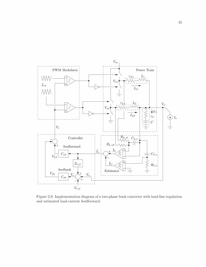
45
IC
Vc
Vin
Power Train
Io
IC
Vo
IL1
L2
L1rL1
rL2
IL2
RL,s1
RL,s2
fsw
PWM Modulator
Vx1
Vx2
C
1rC
1rL
Vfb
Vff
IL
+
−
CL,s
CC,s
RC,s
+
−
+
− +Ve
Cff
Cfb
Vref
−+
Vo
Controller
feedback
feedforwardIo
Estimator
rC
+
−
+
−
Zref
+
−
Figure 2.9: Implementation diagram of a two-phase buck converter with load-line regulationand estimated load-current feedforward.

46
summing the inductor current estimates of the different phases [119, 74], is shown in Fig. 2.9.
In the case of perfect matching of the estimator and power train parameters, the
injection of the load current estimate in the controller does not affect the closed-loop poles
and zeros of the system. In practice, there typically is some mismatch between the estimator
and power train parameters, resulting in the load current estimate becoming a function of
the converter state variables and hence altering the system pole and zero locations. For
small mismatches this effect is small, and can be tolerated in a properly designed controller.
Trace or Package Resistance Sensing
The printed-circuit-board trace resistance connecting the VR to the microproces-
sor, or the package resistance of the microprocessor could be used to sense the load current
as well. The latter approach has been recently developed by Intel for the purposes of on-
chip power management [78]. In [78] the package resistance is calibrated with a precision
on-chip current source. Alternative methods for calibration could be developed using, for
example, the VR input current, since it is relatively easy to measure because of the low
nominal duty ratio.
2.7.4 PWM Modulator
A switch modulation scheme having a very low latency is essential for achieving
a fast controller response with load-current feedforward. Good candidates among fixed-
switching-frequency modulators include unlatched level-sensitive PWM (with some hys-
teresis for noise immunity), leading-edge latched PWM, two-sided latched PWM [56], and
valley current-mode control [85]. All of these have turn-off latency equal to or less than the

47
steady-state on-pulse-width, which is about a tenth of the switching period in 12 V-input
VR’s.
2.7.5 Dynamic Reference Voltage
In this discussion we have assumed that Vref is constant. In modern microprocessor
systems with dynamic voltage scaling, Vref can be adjusted during operation. However, this
happens at slow rates compared to changes in the load current (e.g., reference voltage slew
rate of 2.2 mV/µs, [19]), and hence tracking it does not present a substantial challenge. In
fact, a simple and effective reference voltage feedforward, providing good tracking up to the
LC cutoff frequency, can be accomplished by directly adding Vref to the input of the PWM
modulator.
2.8 Simulations and Experimental Results
To demonstrate the use of load-current feedforward to improve load-line regulation
performance, a 4-phase version of the controller structure in Fig. 2.9 was implemented. A
synchronous buck converter board (International Rectifier IRDCiP2002-C) was modified to
incorporate estimated load-current feedforward. The on-board PWM modulator (Intersil
ISL6558) uses voltage-mode, latched trailing-edge modulation with phase-current balancing.
The converter parameters are summarized in Table 2.2. The feedforward law (2.22) from
Section 2.4.1 was used.
The system was simulated in PSIM (see Appendix A for simulation schematic).
Figures 2.10 and 2.11 show the converter transient response to load steps of different mag-

48
Table 2.2: Prototype 1 MHz buck converter parameters
Power Train
N number of phases 4
Vin input voltage 12 V
Io,max max. load current 120 A
rhφ high-side switch on-resistance 21 mΩ
rlφ low-side switch on-resistance 3 mΩ
Lφ phase inductors 390 nH @ 15 A
rLφ inductor ESR & trace resistance 0.7 mΩ
Cbulk output bulk capacitance 8×100 µF (ceramic)
τCbulk output bulk capacitor ESR time constant 0.2 µs
Chf output high-frequency decoupling capacitance 10 + 0.1 µF (ceramic)
τChf output high-frequency capacitor ESR time constant 24 ns
PID Controller
Vref reference voltage 1.3 V
Rref closed-loop output impedance 1.3 mΩ
fsw switching frequency 1 MHz
K proportional gain 20
TI integral time 17 µs
TD derivative time 3.7 µs
1st high-frequency pole 0.55 MHz
2nd high-frequency pole 1.5 MHz
td control delay before modulator 100 ns
Loop Gain
PM phase margin 47
GM gain margin 10 dB
fc unity gain frequency 200 kHz
nitude, with and without load-current feedforward. In Fig. 2.10 a small 8 A load step is
depicted. With load-current feedforward the output voltage adheres tightly to the pre-
scribed load line [plot (a)]. In plot (b) it can be seen that the feedforward path contributes
the bulk of the duty-ratio command signal, while the feedback signal has a small magni-
tude. In contrast, without load-current feedforward, the control effort is determined solely
by the feedback path, and the output voltage deviates substantially from the desired load

49
line. The feedback unity-gain bandwidth is limited to 200 kHz, which is one-fifth of the
switching frequency, for the stability reasons discussed in Section 2.3.2. However, according
to Section 2.3.2, for the load-line feedback approach to work successfully, the bandwidth has
to be substantially larger than 1/2πRrefC = 153 kHz, which could not be achieved here due
to the stability constraint. Clearly, the load-current feedforward circumvents this limitation
by producing a large, fast, exogenous control signal.
Fig. 2.11 depicts the converter response to a large 52 A load current transient. The
loading transient is a scaled version of the 8 A loading response, since the system has linear
average behavior. The unloading step, however, results in duty-ratio saturation at zero, due
to the low output voltage. The converter behavior under duty-ratio saturation is consistent
with the discussion in Section 2.5. Indeed, solving equation (2.41) for the unloading voltage
overshoot yields ∆Vos = 67 mV which matches the simulation. Notice that, compared to
pure feedback control, the load-current feedforward decreases the output voltage overshoot,
since it drives the duty ratio to saturation faster.
Fig. 2.12 shows the experimental prototype transient response, with and without
estimated load-current feedforward, for 52 A loading and unloading transients, analogously
to Fig. 2.11. Due to hardware constraints of the pulsed load circuit, the loading current step
has a time constant of about 250 ns. The unloading current step is much faster, completing
the step in less than 200 ns.
From the figures it can be seen that the estimated load current follows very well
the measured current with a delay of about 100 ns. The 4 MHz switching noise present
in the load-current estimate results from parasitic coupling to the sense wires which were

50
0 10 20 30 40 501.205
1.21
1.215
1.22
1.225
1.23 (a) Output Voltage
Vo (
V)
w/ feedforwardw/o feedforward
0 10 20 30 40 50−0.8
−0.4
0
0.4
0.8 (b) Duty Ratio Command (AC component)
vol
tage
(V
)
Vff w/ feedforward
Vfb
w/ feedforward V
fb w/o feedforward
0 10 20 30 40 50
60
65
70
(c) Load and Total Inductor Current
cur
rent
(A
)
t (µs)
Io
IL w/ feedforward
IL w/o feedforward
Figure 2.10: Simulated 8 A load transient, from 60 A to 68 A to 60 A, with and withoutload-current feedforward.

51
0 10 20 30 40 501.1
1.15
1.2
1.25
1.3
(a) Output Voltage V
o (V
)
w/ feedforwardw/o feedforward
0 10 20 30 40 50
−4
−2
0
2
4
(b) Duty Ratio Command (AC component)
vol
tage
(V
)
duty−ratio saturation
Vff w/ feedforward
Vfb
w/ feedforward V
fb w/o feedforward
0 10 20 30 40 5040
60
80
100
120
(c) Load and Total Inductor Current
cur
rent
(A
)
t (µs)
Io
IL w/ feedforward
IL w/o feedforward
Figure 2.11: Simulated 52 A load transient, from 60 A to 112 A to 60 A, with and withoutload-current feedforward.

52
w/ feedforwardVo
w/o feedforward
40 A/div
40 A/div
Io
Vo
50 mV/div
1 us/div
^Io
(a) Loading step from 60 A to 112 A
w/o feedforward
Vo50 mV/divw/ feedforward
Vo
40 A/div
40 A/divIo
1 us/div
Io
(b) Unloading step from 112 A to 60 A
Figure 2.12: Experimental 52 A load transient, with corresponding estimated load current,with and without load-current feedforward.

53
Vo
w/o feedforward
8 A/div
w/ feedforward
8 A/div
Vo
10 mV/div
Io
1 us/div
Io
Figure 2.13: Experimental 8 A unloading transient, from 68 A to 60 A, with correspondingestimated load current, with and without load-current feedforward.

54
soldered on top of the converter board. The switching noise does not affect the DC reg-
ulation precision because it is attenuated by the PID controller. Further, in a dedicated
implementation, the sensing can be done through buried PCB traces, thus reducing both
electrostatic and magnetic pickup.
The loading transient in Fig. 2.12(a) resembles closely the simulation in Fig. 2.11.
With pure feedback control the output voltage sags by 35 mV below the load-line, cor-
responding to overshoot of more than 50%. On the other hand, load-current feedforward
effects tight load-line regulation. The unloading transient in Fig. 2.12(b) is similar to the
one in Fig. 2.11 as well. The combined feedback and feedforward control produces a slightly
better voltage response than the feedback alone, implying a faster transition to duty-ratio
saturation. The improvement with feedforward control is not as substantial as that for the
loading transient, since the duty-ratio saturation fundamentally limits the performance. An
overshoot of about 85 mV is observed, which is expected since the duty ratio saturates to
zero about 300 ns after the beginning of the step, and equation (2.41) predicts overshoot
of ∆Vos = 80 mV for these conditions. The transient regulation here can be enhanced if
the synchronous rectifier is turned off, or if a smaller total inductance is used, as discussed
in Section 2.7.1. Finally, Fig. 2.13 shows a smaller, 8 A experimental unloading transient
which parallels the simulation in Fig. 2.10 with some additional sensing and measurement
noise associated with the prototype. Again, it is clear that the combination of feedback and
feedforward provides tighter output impedance regulation than feedback alone.
It should be noted that, while the analysis in the preceding sections assumed that
the load is a variable current source, the load in this experiment is a variable resistor. Thus,

55
the load current is a function of the output voltage, resulting in some positive feedback of
the output voltage through the feedforward control law. The magnitude of this positive
feedback is small compared to the negative feedback gain, and does not result in instability,
as witnessed by the experimental results.
2.9 Conclusion
This chapter presented a consistent framework for output-impedance regulation of
the buck converter using output capacitors with an arbitrary ESR time constant, encompass-
ing electrolytic and ceramic technologies. In both current-mode and voltage-mode control,
load-current feedforward can extend the useful bandwidth beyond that achievable with pure
feedback, since feedforward is not limited by stability constraints. The load-current feed-
forward is used to handle the bulk of the regulation action by providing a fast duty-ratio
control signal. The feedback is used to compensate for imperfections of the feedforward and
to ensure tight DC regulation. With load-current feedforward the output capacitor size is
limited only by large-signal transient and switching-ripple considerations. The load current
can be estimated from the inductor and capacitor voltages with simple RC networks, or
with another lossless sensing method. Different types of PWM modulators can be used as
long as they have low latency. An experimental prototype demonstrated tight load-line reg-
ulation with load-current feedforward, compared to an overshoot of over 50% with feedback
only. These results point to the feasibility of microprocessor VR implementations using
only a small number of ceramic output capacitors. The dynamic load-current feedforward
approach described here for the buck converter can be extended to other converter topolo-

56
gies as well. The discussion was presented in a continuous-time, analog framework, but is
easily convertible to the discrete-time, digital domain. The next chapter discusses some
issues specific to a digital controller implementation.

57
Chapter 3
Digital PWM Controller Design:
Quantization, Limit Cycling, and
Dither
3.1 Introduction
A basic block diagram of a digitally-controlled PWM buck converter is shown
in Fig. 3.1. The controller consists of an analog-to-digital converter (ADC), a discrete-
time control law, and a digital PWM (DPWM) module. The ADC quantizes the regulated
signal (e.g., the output voltage error Ve = Vo − Vref ) into a digital word De. The control law
computes a digital duty-ratio command Dc based on the error De. The DPWM modulator
takes Dc as input, and outputs a PWM waveform with the commanded duty ratio at the
switching frequency fsw. The DPWM waveform has finite time resolution. The sensing and

58
power train
digital controller
Vref
De
Vin
DcADC DPWM
L
C
Vo
lawcontrol
Figure 3.1: Basic block diagram of a digitally-controlled PWM buck converter.
quantization of other variables, such as the load current, can be added depending on the
application and the control law used. Further, interface between the controller and other
digital systems can be included, as indicated in Fig. 1.3 in Chapter 1. The digital controller
can be implemented on an autonomous special-purpose IC [67, 110], integrated in a larger
digital system [101], or programmed on a general-purpose microcontroller or DSP [36].
This chapter discusses implementations of the digital controller blocks, and ad-
dresses system stability issues unique to digital control. Sections 3.2 and 3.3 overview
hardware architectures of ADC and DPWM blocks, respectively. Section 3.4 gives the basic
digital PID control law. Section 3.5 discusses the existence of limit cycles, as well as condi-
tions for their elimination. Section 3.6 introduces digital dither as a method to increase the
effective DPWM resolution, thus preventing limit cycling, and enabling low-power, small-
area DPWM implementations. Section 3.7 provides simulations and experimental results
for a digitally-controlled buck converter, demonstrating the conditions for limit-cycle pre-
vention, and the use of digital dither to increase the effective DPWM resolution. Finally,
Section 3.8 concludes the chapter.

59
3.2 Overview of ADC Topologies
One choice to sample Vo could use an ADC that quantizes the full possible output
range from ground to Vin [107]. An 11-bit ADC will provide 6 mV resolution for Vin = 12 V.
This approach is not well suited for low-power applications, since a high quantization resolu-
tion over a wide voltage range is required. For very low power applications, the ADC can be
implemented with a single comparator [23, 22]. However, this approach has poor transient
performance, since excursions of the output voltage away from the reference voltage cannot
be quantized appropriately. A compromise solution is based on the observation that under
normal operation the output voltage of a regulator should not deviate substantially from
the reference voltage. Thus, the output voltage has to be quantized only over the regulation
window around the reference signal [77]. For example, in microprocessor voltage regulators
the output voltage should be within ±25 mV of the reference signal [19]. Assuming 5 mV
ADC quantization bin size, only 10 bins are required in this case. A block-diagram of a
flash implementation of such a “window” ADC is shown in Fig. 3.2. Note that, since Vo is
compared against Vref , the resulting digital signal (De) is the difference between the two,
which is a digital representation of the error signal Ve. Hence, it has the functionality of
both an ADC and an error amplifier. The window concept has been successfully used in
delay-line [67] and differential-ring-oscillator-counter [110] ADC implementations.
Another consideration for ADC design is sensitivity to noise. A switching con-
verter power train is an inherently noisy environment with high-slew-rate, supply-swing
voltage switching and often substantial inductor ripple currents. Consequently, there is
the possibility of capacitive, inductive, and ground-plane coupling of switching noise to

60
Vadc
Vadc/2
Vadc/2
Vadc
Vref
Vadc
De
Vo
∆
Vadc
comparators
∆
∆
∆
∆
∆
Figure 3.2: Block diagram of a flash window ADC. It implements both an ADC and anerror amplifier.
the ADC input. The switching noise can produce undesirable aliasing effects in the quan-
tization process. For example, typically the ADC is sampled at the converter switching
frequency, and hence switching-frequency noise could be aliased to a DC offset. To prevent
aliasing effects and to provide accurate DC regulation, ADC’s which average the input sig-
nal over each sampling period are desirable. Averaging ADC’s has been implemented with
ring-oscillator-counter [101] and differential-ring-oscillator-counter [110] topologies.
Finally, the converter control strategy may use other system variables besides the
output voltage. For example, the load-current feedforward method discussed in Section 2.4
would require quantization of the load current. In the cases when very fast transient response
is required, the load current may have to be sampled at rates higher than the switching
frequency. Note that with voltage-mode control the feedforward control law (2.22) is AC-
coupled. The AC-coupling can be implemented before the ADC, thus a window architecture

61
could be used for this application as well.
3.3 Overview of Digital PWM Topologies
Two types of structures have been used to implement digital PWM modulators:
counter-comparator [99, 100] and delay-line-mux or ring-oscillator-mux [23]. The counter-
comparator scheme has small area but high power due to high-frequency clocking of the
counter. The ring-oscillator-mux and delay-line-mux schemes have low power, since switch-
ing activity is at the converter switching frequency, however they have large area due to
the large number of delay stages needed. Hybrid systems combining a ring-oscillator-mux
block with a counter-comparator have emerged as a compromise, having acceptable area
and power [22, 101, 67]. A ring-oscillator-mux-dither approach using current-starved dif-
ferential inverters, operating in the sub-threshold regime, has been developed in [108, 110].
Digital cells in the sub-threshold regime have large delay, enabling a small-area ring oscilla-
tor running at the switching frequency. The low DPWM resolution resulting from the long
cell delay is boosted by digital dither [73] (see also Section 3.6).
3.4 Digital Feedback Control Law
A standard choice for the feedback control law is the PID law (2.6) given in Section
2.3.2. Its discrete-time counterpart has the form
Dc[k + 1] = KpDe[k] + Kd (De[k] − De[k − 1]) + KiDi[k], (3.1)

62
where Dc[k] is the duty-ratio command at discrete time k, De[k] is the digitized version of
the error signal Ve, and Di[k] is the state of a digital integrator
Di[k + 1] = Di[k] + De[k]. (3.2)
Parameter Kp is the proportional gain, Kd is the derivative gain, and Ki is the integral
gain. It is often practical to round off the gains to powers of two, allowing for implemen-
tations using simple binary shifts. The design methodologies for digital PID control laws
are discussed in a general framework in [31] and [7], and in a power electronics framework
in [52] and [26], for example. The control law can be implemented with a set of binary
adders and shifts [110]; with a look-up table [67]; or with a microprocessor core (if more
sophisticated computations are required).
Typically, the duty-ratio command is computed once per switching period. How-
ever, if faster response is required, it could be computed more frequently. For example, in
an N -phase converter Dc could be updated at the effective switching frequency Nfsw (this
approach is used in the prototype in Section 4.4).
3.5 Existence and Elimination of Limit Cycles
For the converter of Fig. 3.1, limit cycles refer to steady-state oscillations of Vo
and other system variables at frequencies lower than the converter switching frequency fsw
(subharmonic frequencies). Limit cycles may result from the presence of signal amplitude
quantizers like the ADC and DPWM modules in the feedback loop [107]. Steady-state
limit cycling may be undesirable if it leads to large, unpredicted output voltage variations.
Furthermore, since the limit cycle amplitude and frequency are hard to predict, it is difficult

63
to analyze and compensate for the resulting Vo noise and the electro-magnetic interference
(EMI) produced by the converter.
Let us consider a system with effective ADC resolution of Nadc bits and DPWM
resolution of Ndpwm bits. For a buck converter, this corresponds to voltage quantization of
∆Vadc = Vin/2Nadc steps for the ADC. The DPWM modulator will have a T/2Ndpwm time
resolution, implying ∆Vdpwm = Vin/2Ndpwm output voltage resolution. Fig. 3.3(a) illustrates
qualitatively the behavior of Vo in steady state when the DPWM resolution is less than the
ADC resolution, and there is no DPWM level that maps into the ADC bin corresponding
to the reference voltage Vref (this ADC bin will be referred to as the zero-error bin). In
steady state, the controller will be attempting to drive Vo to the zero-error bin, however due
to the lack of a DPWM level there, it will alternate between the adjacent DPWM levels.
This results in non-equilibrium behavior, such as steady-state limit cycling.
The first step towards eliminating limit cycles is to ensure that under all circum-
stances there is a DPWM level that maps into the zero-error bin. This can be guaranteed
if the resolution of the DPWM module is finer than the resolution of the ADC,
No Limit Cycle Condition # 1
∆Vdpwm < ∆Vadc (3.3)
A one-bit difference in the resolutions, Ndpwm = Nadc + 1, seems sufficient in most applica-
tions since it provides two DPWM levels per one ADC level.
Yet, even if the above condition is met, limit cycling may still occur if the feed-
forward term is not perfect and the control law has no integral term (Ki = 0). In this
case, the controller relies on non-zero error signal De to drive Vo towards the zero-error bin.

64
Vo
−2 LSB error bin
−1 LSB error bin
0 LSB error bin
1 LSB error bin
transient time
Vref
steady state
ADC levelsDPWM levels
voltage
(a)
Vo
−2 LSB error bin
−1 LSB error bin
0 LSB error bin
1 LSB error bin
transient
ADC levels
Vref
steady state
DPWM levels
time
voltage
(b)
Figure 3.3: Qualitative behavior of Vo with (a) DPWM resolution lower than the ADCresolution, and (b) DPWM resolution two times the ADC resolution and with integral termincluded in control law. (The fsw switching ripple is not shown, for clarity.)

65
However, once Vo is in the zero-error bin, the error signal becomes zero, and Vo droops back
below the zero-error bin. This sequence repeats over and over again, resulting in a limit
cycle. This problem can be solved by the inclusion of an integral term in the control law.
After a transient, the integrator will gradually converge to a value that drives Vo into the
zero-error bin, where it will remain as long as De = 0, since a digital integrator is perfect
[Fig. 3.3(b)],
No Limit Cycle Condition # 2
0 < Ki ≤ 1 (3.4)
An upper bound of unity is imposed on the integral gain, since the digital integrator is
intended to fine-tune the output voltage, therefore it has to be able to adjust the duty-ratio
command by steps as small as a least significant bit (LSB).
The two conditions suggested above are not sufficient for the elimination of limit
cycles, since the non-linearity of the quantizers in the feedback loop may still cause limit
cycling for high loop gains. Non-linear system analysis tools, such as describing functions
[32, 31], can be used to determine the maximum allowable loop gain not inducing limit
cycles. The feedback loop includes two quantizers—the ADC and the DPWM—however in
the present analysis we will consider only the ADC non-linearity, since it performs coarser
quantization if the DPWM resolution is made higher than that of the ADC (as recommended
above). The describing function of an ADC (a round-off quantizer) represents its effective
gain as a function of the input signal AC amplitude and DC bias. When the control law
contains an integral term, only limit cycles that have zero DC component can be stable,
because the integrator drives the DC component of the error signal to the zero-error bin.

66
Since in steady state the DC bias is driven to zero, and since the loop gain L(jω) from the
output of the ADC to its input has a low-pass characteristic, the sinusoidal-input describing
function of a round-off quantizer can be used to analyze the stability of the system. The
characteristic of a round-off quantizer is plotted in Fig. 3.4(a), where Vadc is the ADC input
voltage, ∆Vadc is the ADC quantization bin size corresponding to one LSB, and Dout is the
quantized representation of Vadc. The corresponding describing function N (A) is plotted
in Fig. 3.4(b), where A is the AC amplitude of Vadc. From the plot it can be seen that the
describing function has a maximum value of about 1.3, corresponding to maximum effective
ADC gain. The control law (3.1), and hence L(jω), can then be designed to exclude limit
cycles by ensuring that
No Limit Cycle Condition # 3
1 + N (A)L(jω) = 0 (3.5)
(Nyquist Criterion)
holds for all non-zero finite signal amplitudes A and frequencies ω. In practice, conventional
loop design methods (e.g., Bode plots) can be used, keeping in mind that the effective ADC
gain peaks somewhat above unity.
The no-limit-cycle conditions have been further explored in [68] with a more de-
tailed analysis, largely corroborating the considerations discussed above.
3.6 Digital Dither
The precision with which a digital controller regulates the steady-state Vo is de-
termined by the resolution of the ADC. In particular, Vo can be regulated with a tolerance

67
−6 −4 −2 0 2 4 6−6
−4
−2
0
2
4
6
Vadc / ∆Vadc (LSB)
Dou
t (L
SB)
(a)
0 1 2 3 4 5 60
0.2
0.4
0.6
0.8
1
1.2
A / ∆ Vadc (LSB)
N
(A)
(b)
Figure 3.4: Characteristic of a round-off quantizer (a), and the corresponding describingfunction for sinusoidal signals with zero DC bias (b).

68
of one LSB of the ADC. Many present-day applications, such as microprocessor VR’s, de-
mand tight regulation tolerances [19], requiring ADC and DPWM modules with very high
resolution. For example, regulation resolution of 10mV at Vin = 12V corresponds to ADC
resolution of Nadc = log2(12 V/10 mV)≈10 bits, implying DPWM resolution of at least
Ndpwm = 11 bits to avoid limit-cycling. For a converter switching frequency of fsw = 1
MHz, such resolution would require a 211fsw = 2 GHz fast clock in a counter-comparator
DPWM implementation, or 211 = 2048 stages in a ring-oscillator implementation, resulting
in high power dissipation or large area, respectively [101, 22]. Thus, it is beneficial to look
for ways to use low-resolution DPWM modules to achieve the desired high Vo resolution.
One method which can increase the effective resolution of a DPWM module is
dithering. It amounts to adding high-frequency periodic or random signals to a certain
quantized signal, which is later filtered to produce average DC levels with increased resolu-
tion. Analog dither has been used to increase the effective resolution of a DPWM module
[14]. However, analog dither is difficult to generate and control, it is sensitive to analog
component variations, and it can be mixed only with analog signals in the converter, and
not with signals inside a digital controller. On the other hand, digital dither generated
inside the controller is simpler to implement and control, is insensitive to analog component
variations, and can offer more flexibility. Therefore, the use of digital dither to improve the
resolution of DPWM hardware is discussed in the present section.
3.6.1 Programmed Digital Dither
The idea behind programmed digital dither is to vary the duty ratio by an LSB
over a few switching periods, in a pre-determined way, so that the average duty ratio has a

69
value between two adjacent quantized levels. The averaging action is implemented by the
output LC filter. The dither concept is illustrated in Fig. 3.5. Let Dc1 and Dc2 correspond to
two adjacent quantized duty-ratio levels put out by the DPWM module, Dc2 = Dc1 + LSB.
If the duty ratio is made to alternate between Dc1 and Dc2 every next switching period,
the average duty ratio over time will equal (Dc1 + Dc2)/2 = Dc1 + (1/2)LSB. Thus, an
intermediate (1/2)LSB sub-LSB level can be implemented by averaging over two switching
periods, resulting in a one-bit increase of the effective DPWM resolution. Using the same
reasoning, (1/4)LSB and (3/4)LSB levels can be implemented by averaging over four
switching periods (Fig. 3.6), which increases the effective DPWM resolution by two bits.
Finally, it can be seen that by using dither patterns spanning 2Ndith switching periods, the
effective DPWM resolution can be increased by Ndith bits,
Ndpwm,eff = Ndpwm + Ndith, (3.6)
where Ndpwm is the hardware DPWM resolution, and Ndpwm,eff is the effective DPWM
resolution.
Of course, the effective increase in DPWM resolution by dithering does not come
for free. The dithering of the duty ratio creates an additional AC ripple at the output of
the LC filter, which is superimposed on the ripple from the converter switching action. It
is desirable to keep the amplitude of the dither ripple low, in order to avoid poor output
regulation, EMI, and limit cycles which may result from the interaction between the dither
ripple and the ADC. Thus, it is beneficial to select dither patterns that minimize the dither
ripple. For this reason we have restricted the discussion to dither with one LSB amplitude.
For a dither sequence with a particular length (2Ndith switching cycles for Ndith-bit
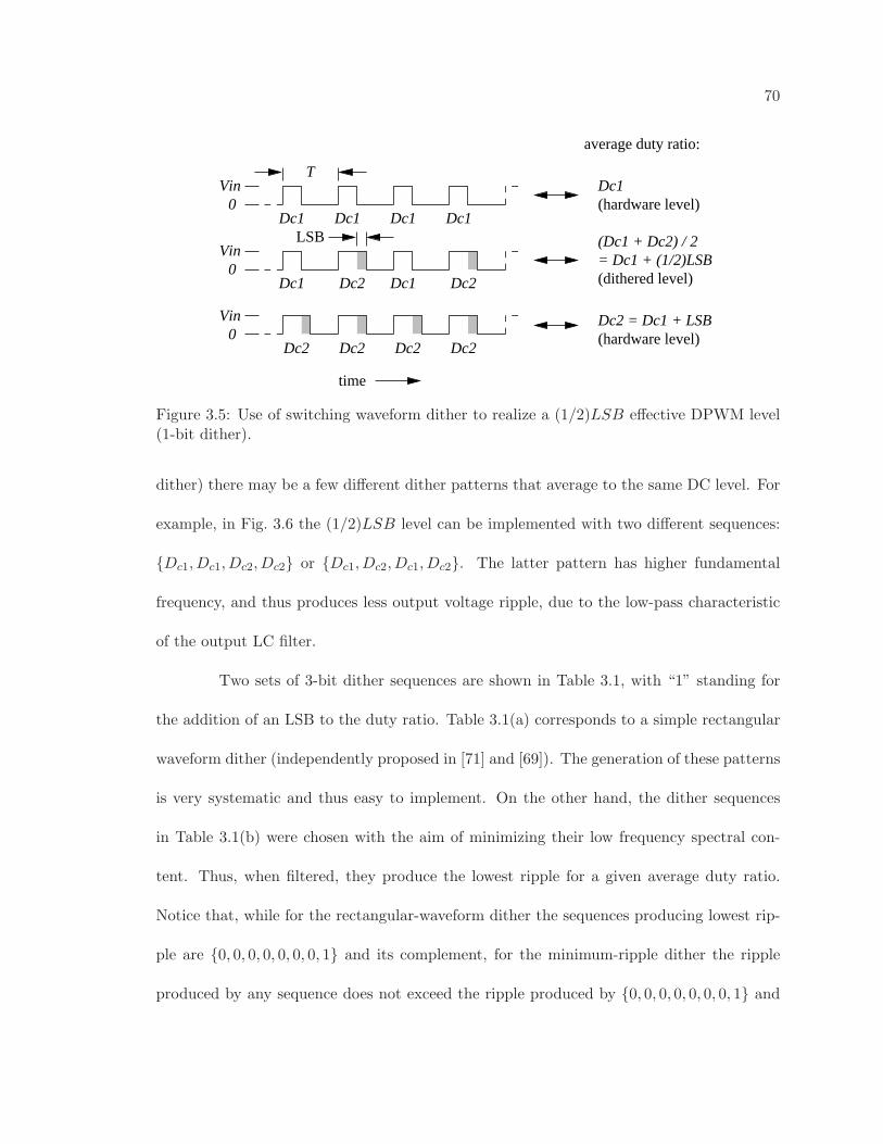
70
time
LSB
0
Vin0
Vin0
Dc1
(hardware level)
(Dc1 + Dc2) / 2= Dc1 + (1/2)LSB
Dc2 = Dc1 + LSB
(hardware level)
(dithered level)
average duty ratio:
Dc1
VinT
Dc1Dc1Dc1
Dc1 Dc2 Dc1 Dc2
Dc2Dc2Dc2Dc2
Figure 3.5: Use of switching waveform dither to realize a (1/2)LSB effective DPWM level(1-bit dither).
dither) there may be a few different dither patterns that average to the same DC level. For
example, in Fig. 3.6 the (1/2)LSB level can be implemented with two different sequences:
Dc1, Dc1, Dc2, Dc2 or Dc1, Dc2, Dc1, Dc2. The latter pattern has higher fundamental
frequency, and thus produces less output voltage ripple, due to the low-pass characteristic
of the output LC filter.
Two sets of 3-bit dither sequences are shown in Table 3.1, with “1” standing for
the addition of an LSB to the duty ratio. Table 3.1(a) corresponds to a simple rectangular
waveform dither (independently proposed in [71] and [69]). The generation of these patterns
is very systematic and thus easy to implement. On the other hand, the dither sequences
in Table 3.1(b) were chosen with the aim of minimizing their low frequency spectral con-
tent. Thus, when filtered, they produce the lowest ripple for a given average duty ratio.
Notice that, while for the rectangular-waveform dither the sequences producing lowest rip-
ple are 0, 0, 0, 0, 0, 0, 0, 1 and its complement, for the minimum-ripple dither the ripple
produced by any sequence does not exceed the ripple produced by 0, 0, 0, 0, 0, 0, 0, 1 and
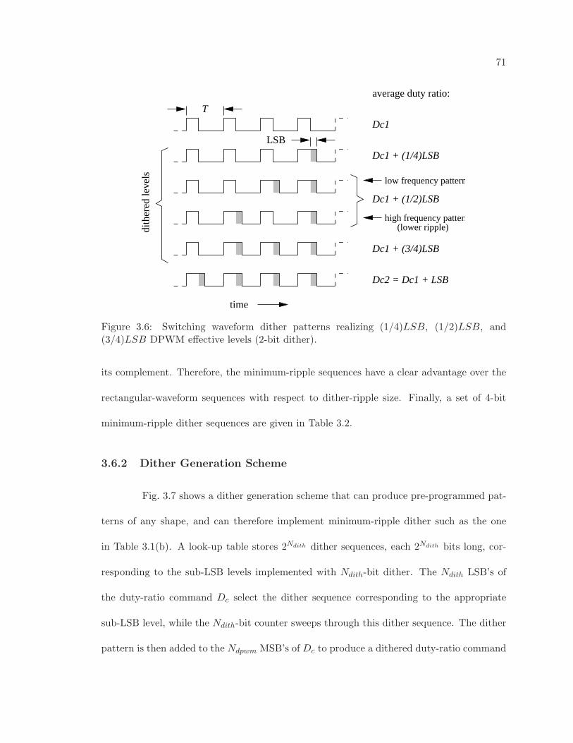
71
T
LSBdi
ther
ed le
vels
(lower ripple)high frequency pattern
low frequency pattern
average duty ratio:
Dc1 + (1/2)LSB
time
Dc2 = Dc1 + LSB
Dc1 + (3/4)LSB
Dc1 + (1/4)LSB
Dc1
Figure 3.6: Switching waveform dither patterns realizing (1/4)LSB, (1/2)LSB, and(3/4)LSB DPWM effective levels (2-bit dither).
its complement. Therefore, the minimum-ripple sequences have a clear advantage over the
rectangular-waveform sequences with respect to dither-ripple size. Finally, a set of 4-bit
minimum-ripple dither sequences are given in Table 3.2.
3.6.2 Dither Generation Scheme
Fig. 3.7 shows a dither generation scheme that can produce pre-programmed pat-
terns of any shape, and can therefore implement minimum-ripple dither such as the one
in Table 3.1(b). A look-up table stores 2Ndith dither sequences, each 2Ndith bits long, cor-
responding to the sub-LSB levels implemented with Ndith-bit dither. The Ndith LSB’s of
the duty-ratio command Dc select the dither sequence corresponding to the appropriate
sub-LSB level, while the Ndith-bit counter sweeps through this dither sequence. The dither
pattern is then added to the Ndpwm MSB’s of Dc to produce a dithered duty-ratio command

72
Table 3.1: 3-bit dither sequences
Sequence Average Rectangular-waveform Sequence Ripple Minimum-ripple Sequence Ripple
0/8 0 0 0 0 0 0 0 0 none 0 0 0 0 0 0 0 0 none
1/8 0 0 0 0 0 0 0 1 lowest 0 0 0 0 0 0 0 1 highest
2/8 0 0 0 0 0 0 1 1 0 0 0 1 0 0 0 1
3/8 0 0 0 0 0 1 1 1 0 0 1 0 0 1 0 1
4/8 0 0 0 0 1 1 1 1 highest 0 1 0 1 0 1 0 1 lowest
5/8 0 0 0 1 1 1 1 1 0 1 0 1 1 0 1 1
6/8 0 0 1 1 1 1 1 1 0 1 1 1 0 1 1 1
7/8 0 1 1 1 1 1 1 1 lowest 0 1 1 1 1 1 1 1 highest
2 x 2Ndith Ndith
f
Ndith(LSB’s)
sw
1(LSB)Ndpwm
from
Ndith
control law
to DPWMmodulator
table
Dc’
Dc
Ndpwm (MSB’s)
Ndpwm + NdithNdpwm−bit
saturated
adderlook−up
counterNdith−bit
Figure 3.7: Structure for adding arbitrary dither patterns to the duty ratio, boosting theeffective DPWM resolution by Ndith bits.
D′c which is sent to the hardware DPWM module.
Note that it is generally true that the dither sequences with averages of 1/2 + 1/2Ndith
to 1 − 1/2Ndith are the inverses of the sequences with averages of 1/2 − 1/2Ndith to 1/2Ndith
(in reverse order). For example, in Table 3.2 the 9/16 to 15/16 dither sequences are the
inverses of the 7/16 to 1/16 sequences. Further, the 0/2Ndith dither level corresponds to a
zero sequence. Thus, only 2Ndith−1 unique dither sequences have to be stored in the look-up

73
Table 3.2: 4-bit minimum-ripple dither sequence
Sequence Average Dither Sequence
0/16 0 0 0 0 0 0 0 0 0 0 0 0 0 0 0 0
1/16 0 0 0 0 0 0 0 0 0 0 0 0 0 0 0 1
2/16 0 0 0 0 0 0 0 1 0 0 0 0 0 0 0 1
3/16 0 0 0 0 0 1 0 0 0 0 1 0 0 0 0 1
4/16 0 0 0 1 0 0 0 1 0 0 0 1 0 0 0 1
5/16 0 0 0 1 0 0 1 0 0 1 0 0 1 0 0 1
6/16 0 0 1 0 0 1 0 1 0 0 1 0 0 1 0 1
7/16 0 0 1 0 1 0 1 0 0 1 0 1 0 1 0 1
8/16 0 1 0 1 0 1 0 1 0 1 0 1 0 1 0 1
9/16 1 1 0 1 0 1 0 1 1 0 1 0 1 0 1 0
10/16 1 1 0 1 1 0 1 0 1 1 0 1 1 0 1 0
11/16 1 1 1 0 1 1 0 1 1 0 1 1 0 1 1 0
12/16 1 1 1 0 1 1 1 0 1 1 1 0 1 1 1 0
13/16 1 1 1 1 1 0 1 1 1 1 0 1 1 1 1 0
14/16 1 1 1 1 1 1 1 0 1 1 1 1 1 1 1 0
15/16 1 1 1 1 1 1 1 1 1 1 1 1 1 1 1 0
table, and the rest can be generated from them via simple logic operations.
3.6.3 Dither Ripple and Bit Limit
In Section 3.6.1 it was shown that the longer the dither patterns used, the larger
the effective DPWM resolution. However, longer dither patterns could cause higher output
ripple, since they contain lower frequency components, receiving less LC-filter attenuation.
This consideration puts a practical limit on the number of bits of dither that can be added

74
∆
∆V dpwm,eff
adcV
ADC level maximum dither ripple amplitude
effective DPWMlevel
center of ADC bin
Figure 3.8: Maximum dither ripple amplitude constraint. Illustrated case is for Ndpwm,eff =Nadc + 2.
to increase the DPWM resolution.
To ensure that the dither does not cause steady-state limit cycling, there should
always be an effective DPWM level that completely fits into one ADC quantization bin,
taking into account the dither ripple. The converter switching ripple is not considered, since
it is synchronous with the ADC sampling, and is thus aliased to a DC offset, which does
not affect the limit cycle. With Ndith-bit dither, the effective DPWM quantization bin size
is
∆Vdpwm,eff = Vin/2Ndpwm,eff = Vin/2Ndpwm+Ndith . (3.7)
Geometric considerations show that the case which allows for the smallest dither ripple
amplitude is when the effective DPWM levels are located at one-half effective DPWM bin
size from the center of the ADC bin (see Fig. 3.8). Then the tolerable peak-to-peak dither
ripple amplitude is bounded by
∆Vo,dith < ∆Vadc − ∆Vdpwm,eff . (3.8)
Assuming that the ADC has resolution ∆N bits coarser than the effective DPWM resolu-

75
tion,
Nadc = Ndpwm,eff − ∆N = Ndpwm + Ndith − ∆N, (3.9)
the ADC bin size is
∆Vadc = Vin/2Nadc = Vin/2Ndpwm+Ndith−∆N . (3.10)
Substituting (3.7) and (3.10) in (3.8), we obtain
∆Vo,dith < Vin
(2∆N − 1
)/2Ndpwm+Ndith . (3.11)
To determine how many bits of dither can be used in a certain converter, without causing
a limit cycle, we now have to calculate ∆Vo,dith as a function of Ndith.
The dither ripple at the output depends on the DPWM resolution, the power
train parameters, and the dither temporal pattern. Since the dither constitutes switching
between two adjacent quantized duty-ratio levels, it can be modeled as a rectangular wave-
form, injected in the converter switching node, with peak-to-peak amplitude of one DPWM
hardware LSB, equal to Vin/2Ndpwm . Further, the fundamental dither frequency component
is
fdith = fsw/2Ndith . (3.12)
We will study the ripple size and the corresponding number of bits of dither that can be
used for the two dither schemes in Table 3.1.
Rectangular Dither
For the rectangular-waveform dither in Table 3.1(a), the dither waveform with the
largest low frequency component is a square wave with 50% duty ratio. This waveform can

76
be used to study the worst-case dither ripple. Since the dither is smoothed by the power
train LC filter, we will consider only its fundamental frequency component, which is a sine
wave with frequency fdith and peak-to-peak amplitude
Ap−p,dith =4π
Vin
2Ndpwm. (3.13)
The peak-to-peak output voltage ripple can then be bounded approximately as
∆Vo,dith ≤ |G(j2πfdith)|Ap−p,dith, (3.14)
where G(s) is the power train control-to-output voltage transfer function (2.4) from Section
2.3.2. Above the power train cutoff frequency fc = 1/2π√
LC, the magnitude of (2.4) is
approximately
|G(j2πfdith)| ≈
(fc
f
)2, fc < f < fz, (−40dB/dec rolloff)
fc2
fzf , fz < f, (−20dB/dec rolloff)(3.15)
where fz = 1/2πτC is the capacitor ESR zero frequency. Substituting back in (3.14), we
derive the worst-case peak-to-peak output voltage ripple due to dither,
∆Vo,dith ≈
(fc
fsw
)222Ndith 4
πVin
2Ndpwm
, fc < fdith < fz,
fc2
fzfsw2Ndith 4
πVin
2Ndpwm
, fz < fdith.
(3.16)
This ripple approximation is a slight underestimate, since the higher order harmonics are
ignored in (3.14), and (3.15) overestimates the attenuation in the vicinity of fc and fz.
However, it enables the derivation of an analytical condition on how many bits of dither,
Ndith, can be used in a certain system. Combining (3.11) with (3.16), and solving for Ndith,
we obtain an upper bound,
Ndith <
13 log2
[π4
(fsw
fc
)2(2∆N − 1)
], fc < fdith < fz,
12 log2
[π4
fzfsw
fc2 (2∆N − 1)
], fz < fdith,
(3.17)

77
The above equation can be used by starting with a guess for Ndith, obtaining the corre-
sponding dither frequency from (3.12), and then using (3.17) to obtain a bound on Ndith. If
the result is not consistent with the initial guess for Ndith, the procedure should be repeated
with a reduced value of Ndith. On the other hand, if the inequalities are satisfied, the value
of Ndith can be increased, and the procedure can be repeated.
Minimum-Ripple Dither
For the minimum-ripple dither in Table 3.1(a), the dither sequences producing
the largest ripple are the one consisting of all ”0”’s and a single ”1” [(1/8) LSB], and its
complement [(7/8) LSB]. Since these dither patterns have an asymmetric duty cycle, they
contain significant spectral energy in harmonics beyond the fundamental. Thus, performing
analysis based solely on the fundamental frequency component will yield inaccurate results.
Therefore, we adopt a time domain analysis approach based on calculating the ripple charge
delivered onto the output capacitor.
First, we calculate the inductor current ripple contributed by the dither. Let the
duty-ratio command without dither be Dc. When one LSB is added by the dither, the
duty ratio becomes Dc1 = Dc + 1/2Ndpwm . For Ndith-bit dither, the sequence consisting of
all ”0”’s and a single ”1” produces average output voltage
Vo = (Dc + 1/2Ndpwm+Ndith)Vin. (3.18)
Thus, the peak-to-peak current ripple contributed by this dither pattern is
∆IL,dith =T
L
(Dc1Vin − Vo
)=
TVin
L2Ndpwm
(1 − 1
2Ndith
). (3.19)

78
The resulting ripple charge delivered onto the output capacitor is
∆QC,dith =T2Ndith∆IL,dith
8, (3.20)
resulting in capacitor voltage ripple
∆VC,dith =∆QC,dith
C=
T2Ndith∆IL,dith
8C. (3.21)
The total dither ripple at the output, taking into account the capacitor ESR is
∆Vo,dith ≈(
T
82Ndith + τC
)∆IL,dith
C
=(
1 +4π
fsw
fz
12Ndith
) (fc
fsw
)2 (2Ndith − 1
) π2
2Vin
2Ndpwm.
(3.22)
This ripple approximation is a slight overestimate, since the capacitor and ESR voltage
ripples are assumed to be in phase. Combining (3.11) with (3.22), and solving for Ndith, we
obtain an upper bound,
Ndith < log2
1 − 4
π
fsw
fz+
√(4π
fsw
fz+ 1
)2
+8(2∆N − 1)
π2
(fsw
fc
)2 − 1. (3.23)
Fig. 3.9 compares the number of bits of dither that can be used with rectangular
(3.17) and minimum-ripple (3.23) dither schemes. The plot shows Ndith as a function of the
ratio of power train cutoff frequency to the switching frequency fc/fsw. It covers the range
of 0.01 to 0.1 for fc/fsw, which is typical for voltage regulators for digital applications.
The capacitor ESR zero frequency is fixed to fz = 0.5fsw, which is consistent with ceramic
capacitor technology at switching frequencies of about one megahertz. It is assumed that the
effective DPWM resolution is one bit higher than the ADC resolution (∆N = 1). The plot
indicates that using the minimum-ripple dither is advantageous, since it generally allows
for the use of more dither bits than does rectangular dither, and hence enables the use of
lower-resolution DPWM hardware.

79
0.01 0.02 0.03 0.04 0.05 0.06 0.08 0.1
2
3
4
5
fc / f
sw
Ndi
th (
bit)
minimum−ripple ditherrectangular dither
Figure 3.9: Dither bit limit vs. power train cutoff frequency, for fz = 0.5fsw and ∆N = 1.
3.6.4 Multi-phase Dither
The concept of programmed dither can be extended to multi-phase (interleaved)
converters like the one given in Fig. 2.1. The programmed-dither technique developed for
single-phase converters can be applied directly to the multi-phase case. For example, to
achieve a Dc1 + (1/2)LSB level, duty ratio Dc1 is applied to all phases for one switching
period, followed by Dc2 = Dc1 + LSB applied to all phases, and so on. However, in a
multi-phase converter we can exploit the additional degrees of freedom associated with the
independent switching of the phases to further reduce the dither ripple. This would allow
for more bits of dither, and consequently less bits of hardware DPWM resolution.
Consider again the case of a Dc1 +(1/2)LSB level. This level can be implemented

80
all phases =
time =averaged over
duty ratio
time
phase 1
phase 2
phase 3
phase 4
Dc1+LSB
averaged overduty ratio
Dc1 + (1/2)LSB
Dc1 + (1/2)LSB
Dc[k+3]Dc[k+2]Dc[k+1]Dc[k]
Dc1
Figure 3.10: Four-phase switching waveform dither patterns implementing a (1/2)LSBeffective DPWM level.
by commanding, in the same switching period, Dc1 to two of the phases and Dc2 to the
other two, so that the average duty ratio over all phases is Dc1 +(1/2)LSB for that period.
The next switching period the duty ratio commands are toggled, so that the average over
all phases is still Dc1 + (1/2)LSB, however the average over time for each phase is Dc1 +
(1/2)LSB as well (Fig. 3.10). The equal averaging over time for each phase is necessary
to avoid DC current mismatch among the phases. This approach can be extended for
other sub-LSB levels as well. In general, for an N -phase converter, log2N bits of dither
can be implemented by averaging over the phases. Multi-phase dither can increase the
dither frequency seen at the output node about N times, thus reducing the resulting ripple,
and allowing approximately log2N more bits of DPWM resolution to be implemented with
dither.

81
3.6.5 Sigma-Delta Dither
An alternative approach to increase the effective resolution of DPWM modulators
uses sigma-delta modulation [48, 66, 49]. For a general discussion of sigma-delta modula-
tion see, for example, [64]. The sigma-delta modulator uses local feedback of the digital
duty-ratio command to generate the dither sequence, and there is no need to store pre-
programmed dither patterns. This approach, however, does not guarantee minimum-ripple
dither, and further the dither spectral content is generally hard to predict.
3.7 Simulations and Experimental Results
A prototype buck converter with parameters given in Table 3.3 was built to verify
the no-limit-cycle conditions outlined in Section 3.5, as well as the use of the programmed
dither from Section 3.6.1. The ADC quantization bin is ∆Vadc = 9.8 mV. Fig. 3.11 shows
the simulated output voltage behavior in steady-state and during a load-current transient.
The results from both a switched simulation and an averaged model are given, both im-
plemented in MATLAB (see Appendix B for MATLAB code). The switched simulation
time step was fixed at one hardware DPWM LSB, T/2Ndpwm = 31.25 ns, which is a natural
choice for a converter with a discrete-time controller. In Fig. 3.11(a) the converter behavior
without an integral feedback term (Ki = 0) is shown. The system exhibits a sub-harmonic
limit cycle since condition (3.4) is not met. Note also that since there is no integral feed-
back, the DC output impedance is non-zero, as predicted by standard linear system theory.
In plot (b) the integrator is enabled, however the 4-bit dither is turned off, resulting in
limit cycling since the resolution of the DPWM (7-bit) is lower than the ADC resolution

82
Table 3.3: Prototype digitally-controlled buck converter parameters
Power Train
N number of phases 4
Vin input voltage 10 V
rs input source impedance 16 mΩ
rhφ high-side switch on-resistance 65 mΩ
rlφ low-side switch on-resistance 12 mΩ
Lφ phase inductors 5.5 µH
rLφ inductor ESR & trace resistance 12 mΩ
Cbulk output bulk capacitance 6×680 µF (tantalum)
τCbulk output bulk capacitor ESR time constant 8.8 µs
Chf output high-frequency decoupling capacitance 6×10 µF (ceramic)
τChf output high-frequency capacitor ESR time constant 0.2 µs
PID Controller
Vref reference voltage 2.5 V
fsw switching frequency 250 kHz
fsamp Vo sampling frequency 250 kHz
Nadc effective ADC resolution 10 bit
Ndpwm DPWM hardware resolution 7 bit
Ndith dither resolution 4 bit (Table 3.2)
Kp proportional gain 25
Ki integral gain 2−1
Kd derivative gain 27
td controller delay 5 µs
fe error amplifier −3 dB bandwidth 135 kHz
Loop Gain
PM phase margin 48
GM gain margin 7 dB
fc unity gain frequency 12 kHz

83
(10-bit), violating condition (3.3). Finally, in plot (c) both the integrator and the dither
are enabled, and all three no-limit-cycle conditions (3.3–3.5) are satisfied (condition (3.5) is
satisfied by design of the loop gain). Consequently, limit cycles are prevented. It should be
noted that in this case the steady-state ripple is only due to the multi-phase switching and
the dither, and it does not exceed a couple of millivolts, compared to about 15 mV without
the dither. Also note that in Fig. 3.11(b) the limit-cycle characteristic changes depending
on the loading, resulting in spectral content that is difficult to predict.
Fig. 3.12 shows the experimental data from the hardware prototype. The experi-
mental data largely corroborates the simulated results. One minor difference is that for the
first 0.8 ms after the load transient in Fig. 3.12(b) the limit cycle has a higher frequency.
This is due to the fact that the power supply providing the input Vin to the experimen-
tal converter has complex output impedance characteristic which was simplified to a real
impedance rs in the model. Further, the experimental setup uses resistive load, while the
simulation uses current source load, which may account for some discrepancy in the results.
Finally, 5-bit programmed dither was successfully used in a low-power digital buck-
converter IC to boost the effective resolution of a ring-oscillator-mux DPWM module from
5-bit to 10-bit [110].
3.8 Conclusion
To avoid limit cycling in digitally-controlled DC-DC converters, the resolution of
the DPWM modulator has to be higher that that of the ADC, and an integral term has to be
used in the feedback control law. The effective resolution of the DPWM modulator can be

84
boosted with digital dither, allowing for low-power, small-area DPWM implementations.
The ripple incurred by the dither limits the number of bits of dither that can be used.
Simulations and experimental results indicate an order of magnitude reduction of the steady-
state output voltage ripple when limit cycling is prevented by the use of dither. This chapter
discussed the digital implementation of the basic voltage regulation loop of a switching
converter. The next chapter demonstrates the use of digital control for more sophisticated
adaptive control tasks.

85
−1 −0.5 0 0.5 1 1.5 2 2.5 3 3.5
2.46
2.48
2.5
2.52 (a) Integrator turned off
Vo (
V)
switched simulationaveraged model
−1 −0.5 0 0.5 1 1.5 2 2.5 3 3.5
2.46
2.48
2.5
2.52 (b) Dither turned off
Vo (
V)
−1 −0.5 0 0.5 1 1.5 2 2.5 3 3.5
2.46
2.48
2.5
2.52 (c) Integrator and dither on
Vo (
V)
t (ms)
Figure 3.11: Simulated steady-state behavior and transient response of the prototype buckconverter with and without integral feedback and dither. Load current steps from 0.5 A to12 A at t = 0.

86
−1 −0.5 0 0.5 1 1.5 2 2.5 3 3.5
2.46
2.48
2.5
2.52 (a) Integrator turned off
Vo (
V)
−1 −0.5 0 0.5 1 1.5 2 2.5 3 3.5
2.46
2.48
2.5
2.52 (b) Dither turned off
Vo (
V)
−1 −0.5 0 0.5 1 1.5 2 2.5 3 3.5
2.46
2.48
2.5
2.52 (c) Integrator and dither on
Vo (
V)
t (ms)
Figure 3.12: Experimental steady-state behavior and transient response of the prototypebuck converter with and without integral feedback and dither. Load current steps from 0.5A to 12 A at t = 0.
87
Chapter 4
Multi-Mode Buck Control with
Adaptive Synchronous Rectifier
Scheduling
4.1 Introduction
As discussed in Chapter 1 improving power-conversion efficiency is of paramount
importance for both battery-operated and line-connected digital applications. The syn-
chronous buck converter (Fig. 4.1) and its multi-phase version (Fig. 2.1 in Chapter 2) are
commonly used to regulate the voltage to digital processors. Under different load condi-
tions there are different optimal gating patterns for the switches. For large load currents
the converter runs in continuous-conduction mode (CCM) characterized by strictly posi-
tive steady-state inductor current. At light load, the converter can run in discontinuous
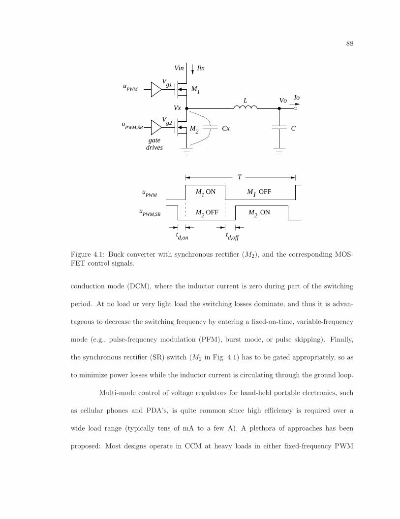
88
1
11 M
2
M
M
VxL Vo Io
M
IinVin
gate
PWM,SRu
PWMu
PWM,SRu
PWMu
C
T
Cx
d,offd,ont t
ON
OFF
OFF
ONM2
2Mg2V
g1V
drives
Figure 4.1: Buck converter with synchronous rectifier (M2), and the corresponding MOS-FET control signals.
conduction mode (DCM), where the inductor current is zero during part of the switching
period. At no load or very light load the switching losses dominate, and thus it is advan-
tageous to decrease the switching frequency by entering a fixed-on-time, variable-frequency
mode (e.g., pulse-frequency modulation (PFM), burst mode, or pulse skipping). Finally,
the synchronous rectifier (SR) switch (M2 in Fig. 4.1) has to be gated appropriately, so as
to minimize power losses while the inductor current is circulating through the ground loop.
Multi-mode control of voltage regulators for hand-held portable electronics, such
as cellular phones and PDA’s, is quite common since high efficiency is required over a
wide load range (typically tens of mA to a few A). A plethora of approaches has been
proposed: Most designs operate in CCM at heavy loads in either fixed-frequency PWM
89
control [79, 63, 110], hysteretic control [4], or fixed-on-time control [98]. At light loads the
converter is typically operated in either PFM [98, 12, 63, 110] or fixed-frequency DCM [79].
Some commercial parts use ”burst-mode” control at light loads, which produces trains of
fixed-frequency pulses followed by off periods [27]. There are also designs that operate in
the same mode at all loads such as variable-frequency DCM [12], and adaptive resonant
fixed-frequency switching [91]. Some approaches gate the SR in DCM [98, 12], while others
turn it off completely [4, 79, 110]. The transition between the low-power and high-power
modes is typically implemented based on some estimate of the load current and possibly
the input voltage [4, 79, 63]. Some controllers use analog implementations [91, 4, 98], while
others are digital [12, 79, 63, 110].
Multi-mode control in higher-power portables such as laptops is less frequent, how-
ever it is becoming increasingly relevant. A method proposed in [17] uses PWM CCM with
SR at heavy loads and can turn off the SR based on a command from the host micro-
processor indicating low-current state. On the other hand, the FAN5093 microprocessor
voltage-regulator IC [88] turns off the SR when negative inductor current is detected, al-
lowing the converter to automatically switch to DCM at light loads. This part also allows
disabling one of its two phases for improved light-load efficiency.
The majority of existing methods for SR control in buck converters rely on high-
bandwidth sensing of the gate and drain voltages of the switch MOSFET’s, using these
signals to adjust the SR timing in order to emulate an ideal diode [39]. For example, an ideal
diode can be emulated by turning on the low-side MOSFET when its drain-source voltage
collapses to zero, and turning off the low-side MOSFET when its drain current decays to

90
zero. The drain current can be sensed via the MOSFET on-state drain-source resistance.
Direct implementations of this approach (e.g., in [39]) could suffer from undesirable body-
diode conduction intervals due to control and MOSFET switching delays.
Adaptive SR methods have been introduced to overcome control and MOSFET
switching delays by predictively setting the SR timing edges based on information from
previous cycles [91, 3, 42]. This technique has been used in a commercial digital implemen-
tation [51]. It still relies on MOSFET gate and drain voltage sensing, which has to be done
on each phase leg in a multi-phase converter, and may require an estimate of the MOSFET
threshold voltage. Further, this method might force the converter in CCM at light loads,
instead of allowing it to enter DCM which is more power efficient.
Since the ultimate objective of SR control is to decrease losses, an alternative
approach is to adjust SR timing so as to directly minimize some measure of the power loss.
This basic idea is behind the method developed in this chapter, and has been pursued in
a number of other works as well. In power electronic systems the perturbation naturally
introduced by the switching action can be used to optimize the system operation on-line
[58, 47], and it has been suggested to use this approach for SR control [38]. However,
this technique cannot successfully adjust parameters which are not directly related to the
switching action, such as the SR dead-times. More recently, a method proposed in [2] steps
the SR dead-time and measures the resulting change in the converter input current which
is related to the efficiency. The dead-time is adjusted in direction of increasing efficiency.
Only turn-on dead-time optimization is demonstrated, with the turn-off dead-time kept
fixed. A similar method proposed in [117] adjusts the SR dead-times so that the duty-ratio

91
command is minimized, corresponding to maximized efficiency. Each dead-time is initially
set to some large value and gradually decreased until the duty-ratio command starts to
increase, at which point the algorithm stops. The algorithm is run subsequently for the
turn-on and turn-off dead-times. It is turned off until a ”large” transient is detected, after
which it is run again. It is suggested that after a transient the algorithm starts from the
point it reached during the previous optimization run. Using the duty-ratio command as a
cost function for the dead-time optimization has the major benefit of not requiring sensing
and analog-to-digital conversion of any additional quantities besides the output voltage.
Unfortunately, the search algorithms in both [2] and [117] have little robustness
to transients and can easily converge to a sub-optimal SR timing pattern in the present
of minor disturbances. Further, the optimization of the turn-on and turn-off dead-times
cannot be done simultaneously. Finally, the speed of convergence to the new optimum after
a load transient is limited by feedback stability constraints of the adaptive loop. These
could be considerable disadvantages in microprocessor voltage regulator applications where
the load current may change rapidly and frequently over a wide range (see Chapter 2).
We present an alternative approach based on controlling (scheduling) the SR tim-
ing as a direct function of load current, since the optimal SR timing depends strongly on
the load current. A load current measurement or estimate is typically available to the con-
troller since it is used for load-line control in VR’s. The function relating the optimal SR
gating to the load current can be determined off-line and programmed in the controller.
Alternatively, it can be obtained on-line by dynamically minimizing the converter power
loss via multi-parameter extremum seeking [41, 40, 96, 5]. The extremum-seeking method

92
introduces perturbations in the parameters which are to be optimized (SR dead-times in
this case) and measures the gradient of a cost function (power loss, or related quantities).
The gradient information is used to adjust the parameters in direction of improving cost
function. Quantities besides the power loss which could be used as cost functions are the
input current, temperature, or the closed-loop duty ratio, as suggested in [117].
This method does not suffer from the sensitivity to transients and the speed lim-
itations of the algorithms in [2] and [117]. The sensitivity to transients is greatly reduced
by demodulating the cost function with the perturbation signal, thus sharply attenuating
disturbances at other frequencies. The load current adjusts the SR dead-times in a direct,
feedforward manner, which is not limited by feedback stability constraints, and can there-
fore provide very fast response to load transients. This capability could be very important
in applications such as modern microprocessor supplies, where the load current can change
with a high frequency and slew rate. Further, this method can optimize multiple variables
(such as the turn-on and turn-off dead-times) simultaneously using orthogonal perturba-
tions. This approach requires only coarse sampling of the scheduling variable (e.g., the
output current) at a rate commensurate with the desired speed of SR timing adjustment.
The inductor current can be used as a scheduling variable instead of the load current. Slow
variations of other converter parameters on which the power loss depends, such as input
(battery) voltage and ambient temperature, are compensated for by the extremum-seeking
algorithm. Only low-bandwidth sensing of the quantity characterizing the converter power
loss is required for the extremum-seeking adaptation. This method is particularly well-
suited for a digital controller implementation, since it uses low-rate computations and data

93
storage, thus not requiring analog-to-digital sampling rates beyond the converter switching
frequency, which is typically in the range of hundreds of kHz to a MHz.
Importantly, with the proposed SR control method, the converter automatically
enters DCM at light loads by virtue of the fact that the power-loss in DCM is lower than in
CCM, and the extremum-seeking algorithm converges there. Further by imposing a mini-
mum duty-ratio, which is straightforward to implement in a digital controller, the converter
will automatically enter pulse-skipping mode at very light loads, effectively decreasing the
switching frequency and the associated switching losses. Thus, the same controller struc-
ture is used in both fixed-frequency PWM and variable-frequency pulse-skipping modes.
In multi-phase converters, some of the phases could be disabled at light loads to further
improve efficiency.
Multi-mode control of buck converters is discussed in Section 4.2. Section 4.3
develops load-current-scheduled SR control with loss-minimizing adaptation, and further
shows how a similar approach could be used for fast duty-ratio adjustment in DCM. Sec-
tion 4.4 demonstrates loss-minimizing scheduled SR control and multi-mode operation on
a digitally-controlled 100 W 4-phase buck converter. Finally, Section 4.5 discusses the
proposed techniques in view of the experimental results.
4.2 Multi-Mode Buck Control
4.2.1 Buck Converter Modes
As discussed in Section 4.1, to ensure high efficiency over a wide load range, the
buck converter could be operated in different modes depending on the load current. A

94
10−1
100
101
102
10−3
10−2
10−1
100
101
Io (A)
td,on*
td,off*
DCM CCM
Fixed Freq.Pulse Skip.
Ton
Teff
Figure 4.2: Timing parameters of the buck-converter control switch and synchronous recti-fier for different modes of operation. All parameters are normalized by the fixed-frequencyswitching period T , and both axes are logarithmic.
representative mode diagram, giving the switches’ timing parameters as a function of load,
is shown in Fig. 4.2. Parameter Teff is the effective switching period, which is equal to
T is fixed-frequency operation (refer to Fig. 4.1). Parameter Ton is the on-time of control
(high-side) switch M1. Parameters t∗d,on and t∗d,off are the optimal turn-on and turn-off
dead-times, respectively, of the SR (low-side) switch M2. The buck modes of operation are
cataloged below:
Fixed-frequency CCM
At heavy load the converter operates in CCM with a fixed switching period T .
The control switch on-time is Ton = DT = MT , where D is the duty ratio, M = Vo/Vin is

95
the conversion ratio, and Vin and Vo are the input and output voltages, respectively. The
optimal turn-off dead time t∗d,off depends on the intrinsic turn-off delay td,off0 of the control
switch M1, and the time it takes to discharge the switching node capacitance Cx,
t∗d,off =VinCx
Io+ td,off0, (4.1)
where Io is the load current. Further, the optimal turn-on dead time t∗d,on is a small constant,
td,on0, preventing conduction overlap between the control switch and the SR.
The power losses in CCM are typically dominated by conduction losses caused by
the load current and the inductor current ripple ∆IL,CCM flowing through the switches and
the inductor [16, Ch. 5], [42],
Ploss,cond,CCM = r′L
(I2o +
112
∆I2L,CCM
), (4.2)
where r′L is the average switch resistance in series with the inductor resistance, and
∆IL,CCM =VinTM(1 − M)
L, (4.3)
where L is the total inductance (all inductors in parallel in a multi-phase converter).
Fixed-frequency DCM
At lighter loads, the converter enters DCM if the SR is gated so that it does not
allow negative inductor currents. This happens below load current
Io,crit =12∆IL,CCM . (4.4)
The duty ratio now depends on the load current,
D =
√2LIoM
VinT (1 − M). (4.5)

96
0 0.2 0.4 0.6 0.8 10
0.2
0.4
0.6
0.8
1
Io / I
o,crit
Plo
ss,c
ond /
Plo
ss,c
ond (
I o,cr
it)
DCMCCM
Figure 4.3: Normalized conduction power loss in discontinuous conduction mode (DCM)and continuous conduction mode (CCM).
The optimal turn-off dead time still follows (4.1). The optimal td,on, on the other hand,
varies substantially as a function of the load current,
t∗d,on = T
(1 − D
M
)+ td,on0. (4.6)
In DCM, this parameter corresponds to the time the inductor current is zero.
It can be shown that the conduction power loss in DCM is
Ploss,cond,DCM =r′L3
(2Io)3/2∆I1/2L,CCM . (4.7)
Fig. 4.3 gives the normalized conduction power loss in CCM (4.2) and DCM (4.7). Clearly,
allowing the converter to enter DCM by appropriately timing the SR at load currents below
Io,crit results in significant power savings.
Variable-Frequency Pulse Skipping
At very light load the converter loss is dominated by switching losses which are
proportional to the switching frequency [16, Ch. 5],
Ploss,sw =[12CxV 2
in + (Cg1 + Cg2)V 2G
]fsw, (4.8)

97
where Cg1 and Cg2 are the high-side and low-side gate capacitances, respectively, and VG is
the gate drive voltage swing. Thus, it is advantageous to allow variable frequency operation
at very light loads. This can be implemented in a straightforward way with a digital
controller by limiting the minimum duty ratio to a value Dmin. (Note that there is an
automatic minimum duty ratio limit of one DPWM hardware LSB.) The duty ratio limit
results in pulse-skipping behavior, effectively varying the switching frequency. The converter
is pulse skipping for
Io <D2
minVinT (1 − M)2LM
, (4.9)
with the average switching period following approximately
Teff ≈ VinT 2on(1 − M)2LIoM
. (4.10)
The pulse width Ton depends on the digital PID parameters and the integrator state. The
integral term forces the average error to zero, thus driving the output voltage periodically
among the −1, 0, and +1 error bins, resulting in a Vo limit cycle centered at the zero-error
bin. Hence, the Vo limit cycle typically has an amplitude of about 2 ADC bins (for examples
see Fig. 4.11(d)–(f) in Section 4.4).
4.2.2 Ancillary Issues
Phase Scaling
In a multi-phase buck converter, which is the architecture typically used in micro-
processor VR’s, additional power savings can be realized at light load by disabling some
of the phases [88]. This approach completely eliminates the switching losses which would
otherwise be contributed by the disabled phase legs.

98
Effectiveness of Synchronous Rectification at Light Load
As discussed in Section 4.1, some low-power converter designs gate the SR in
very-light-load variable-frequency operation, while others turn it off altogether. The choice
depends on the efficiency contribution of the SR. The total energy dissipated in the SR per
pulse with on-time Ton, assuming the SR is on while the inductor current discharges to zero,
is
ESR =rlV
2inT 3
on(1 − M)3
3L2M+ Cg2V
2G + ESR,ctrl, (4.11)
where rl is on-resistance of the SR, and ESR,ctrl is the energy overhead of the SR control
circuit. The first term corresponds to the energy dissipated in the on-resistance of the SR.
The second term corresponds to the gate switching loss. On the other hand, if the SR is
off, the current discharges through the body diode of the low-side switch resulting in energy
loss of
ED =VDVinT 2
on(1 − M)2
2L(M + VD/Vin)+ VinQr, (4.12)
where VD is the body-diode forward voltage, and Qr is the reverse-recovery charge [28, Ch.
4]. For a particular design, it is beneficial to use the SR at light loads if the energy saved
by it is more than the energy dissipated in it, namely, if ED > ESR.
The different modes described in this section are straightforward to implement with
a digital controller. The SR timing can be scheduled as a function of the load current, and
optimized on-line as discussed in the next section. Optimal SR timing ensures appropriate
transition between CCM and DCM. The transition to pulse skipping is automatic, given that
a minimum duty ratio is imposed. Importantly, the PID controller structure does not need
to be modified for the different modes, resulting in a simple implementation. Additional

99
features such as scaling the number of phases and disabling the synchronous rectifier at
light loads can be easily scheduled by the load current as well.
Finally, it should be noted that at light loads there is a design trade-off among the
different possible modes of operation: Pulse skipping and reducing the number of phases
can decrease power loss, at the price of increased output voltage ripple. Fixed-frequency
DCM, on the other hand, has lower ripple, at the expense of higher switching losses. Both
of these alternatives are substantially more efficient than CCM operation.
4.3 Load-Scheduled Loss-Minimizing Synchronous-Rectifier
Control
As discussed above, the SR timing parameters can be scheduled as a function of
the load current. The functions td,on(Io) and td,off (Io) can be derived from theoretical
equations, such as (4.6) and (4.1), or obtained from off-line power-loss measurements, and
programmed into a look-up table. However, these approaches do not compensate for pa-
rameter variability with time and ambient conditions. For example, the optimal SR timing
could change with input (e.g., battery) voltage, temperature, component drift, etc. In this
section we present an adaptive algorithm which resolves these issues by determining the
optimal SR scheduling on-line.
The objective is to adjust the SR timing parameters td,on and td,off so as to
minimize the converter power loss Ploss for each load current value. The algorithm is
identical for td,on and td,off , and therefore, we will present it for a general variable td. We

100
Io3∆Io,lin2∆Io,lin∆Io,lin0
td
θ1
θ2
θ3
θ4
...
w1
w4
w3
w2
01010101
...
Figure 4.4: Piecewise linear function modeling dead-time td(Io) (top), and associated vertexweights (bottom).
parameterize each of the dead-time functions
td = td(Io,Θ) (4.13)
with parameter vector Θ = [θ1, · · · , θm]. In this work we use a piecewise linear function
to implement (4.13), where θ l is the l-th vertex of the function (Fig. 4.4). The m vertices
are positioned at every ∆Io,lin increment of Io. They are weighted by a vector W(Io) =
[w1(Io), · · · , wm(Io)] toward td(Io),
td(Io,Θ) = W(Io)ΘT . (4.14)
101
The w parameters characterize the fractional distance of Io to the two neighboring vertices,
wl = 1 − (Io/∆Io,lin − Io/∆Io,lin),
wl+1 = Io/∆Io,lin − Io/∆Io,lin, (4.15)
wλ = 0, for λ = l, l+1,
(see Fig. 4.4), where the vertex index l is the integer part of Io/∆Io,lin,
l = Io/∆Io,lin, (4.16)
and x is the floor function giving the greatest integer less than or equal to x. Thus the
value of td(Io) is obtained by linear interpolation between the two nearest vertices θl and
θl+1. The increment size ∆Io,lin can be constant or can depend on Io to suit a particular
shape of the fitted function. In the latter case the indexing in (4.16) and (4.15) should be
adjusted appropriately. Other parametrization approaches could be used, such as realizing
(4.13) with a smooth function, and adjusting its parameters (e.g., a polynomial with tunable
coefficients).
To determine the optimal value of the parameter vector, a perturbation-based ex-
tremum seeking algorithm is used. Fig. 4.5 gives a block diagram of the adaptive controller.
The controller introduces small, zero-mean perturbations td in td, at frequency fd, result-
ing in modulation of the converter power loss. This, in turn, produces modulation of the
temperature of the power train, which can be measured with thermal sensors. The transfer
characteristic between the converter power loss and the temperature measurement is mod-
eled by Ft(s). The power loss or temperature measurement is passed through an optional
filter Fp(s) yielding signal p which is to be minimized. Filter Fp can be high-pass, blocking

102
vertex
weighting
power converter
− 1s
w1
θoff,1
...
− 1s
wm
θoff,m
...+
+
...
td,off
+
− 1s
θon,1
...aon
∂p∂td,on
Fp(s)
e−jφd,on
e−jφd,off
t′d,on
t′d,off
td,on
td,on
td,off
td,off
w1
...w1
wm
FI(s) Io
p
Ploss(td,on, td,off , Io)
Γon(s)
− 1s
wm
θon,m
...+
+
...
+
td,on
Io
+
+fd,off
fd,on
Ft(s)
Ploss
t
aoff Γoff (s)∂p
∂td,off
Figure 4.5: Block diagram of synchronous rectifier adaptive control using multi-parameterextremum seeking.

103
the DC level of the signal, since only the AC components of the signal at the perturbation
frequencies are needed for the gradient estimation algorithm [96, 40]. Note that since the
power loss signal p can be AC-coupled, simple window ADC structures could be used to
quantize it [77]. The power loss gradient with respect to the dead-time can be obtained by
demodulating the power loss with a delayed version of the perturbation signal t′d, since
∂p
∂td≈
⟨p · t′d
⟩1/fd
, (4.17)
where 〈•〉1/fdstands for averaging over one perturbation period 1/fd (see [96, 40]). The
delay φd models the lag of the converter and sensor response, and the data acquisition and
processing delay. Optionally, the gradient estimate can be filtered through a low-pass filter
Γ(s) to reduce the 2 × fd ripple resulting from the perturbation signal [96]. Based on the
gradient, the parameter vector is adjusted in a direction which decreases the power loss,
θλ[k + 1] = θλ[k] + α wλ[k] p[k] t′d[k] , for λ = 1, · · · , m. (4.18)
This update law is given in discrete time with index k, which is appropriate for a digital
implementation. Gain α = aTadapt, where Tadapt is the adaptive algorithm time step, is
the discrete-time equivalent of continuous-time parameter a in Fig. 4.5, and determines the
speed of parameter adaptation. Weighting parameter w is given by (4.15), and is hence
non-zero only for λ = l, l + 1. Thus, at each iteration the two vertices of td(Io,Θ) which
bracket the load current are adjusted, according to the vertex distance from Io.1 As a
result, each vertex is adjusted based on gradient information from a 2 × ∆Io,lin current
1Since multiplication by the weighting parameters wλ is applied twice in the adaptive loop, in (4.14)and in (4.18), the adaptive loop gain is varied by a factor of two between the condition when Io is centeredbetween two vertices, and the condition when Io coincides with a vertex. This gain variation does not affectsignificantly the operation of the algorithm, since the adaptation occurs at a slow rate.

104
bracket, resulting in robustness to sensing noise and small undulations of the power loss
characteristic due to parasitic ringing. The load current could be low-pass filtered with FI
before the vertex weighting computation (4.15), thus controlling the speed of response of
the dead-times to load changes. The two perturbation signals td,on and td,off are chosen
to be zero-mean and mutually orthogonal to allow independent estimation of td,on(Io) and
td,off (Io), respectively. The perturbation signals can be sine or square waves at two different
frequencies, for example. Importantly, this algorithm does not need to run fast, since it
computes optimal curves for td,on(Io) and td,off (Io), thus requiring only identification of
the constant or slowly varying parameters describing these functions, and not the rapidly
changing parameters td,on and td,off themselves. The speed of response of the SR timing
parameters is independent of the speed of the perturbation-based adaptation, and is set by
FI which can be made as fast as practical.
In the adaptation problem discussed above there are four time scales: the converter
dynamics, the load current dynamics, the perturbation frequencies, and the parameter
estimator time constant. To ensure parameter convergence to a small neighborhood of their
optimal values, the system has to be designed so that the parameter estimator is slower
than the perturbation signals, which should be slow compared to the converter dynamics
[96]. In some applications, such as microprocessor supplies, the load current can vary at
speeds comparable to the converter dynamics. This variation tends to be rejected by the
adaptive algorithm since it is not correlated with the perturbation signals.
105
4.3.1 Other Applications: Duty-Ratio Adaptation
The SR optimization framework developed above is essentially a type of adaptive
feedforward control. It consists of scheduling a control variable as a feedforward function
of the load current (or any other measured exogenous parameter which varies rapidly over
a wide range), and then adaptively estimating this function. This approach can be applied
to number of other control problems in power converters. For example, from equation (4.5)
in Section 4.2 it is clear that in DCM the steady-state duty-ratio command varies over a
wide range as a function of Io, unlike in CCM where it is ideally constant (D = M). The
duty-ratio control laws discussed in Chapter 2, and transformed to a digital implementation
in Chapter 3, are designed for operation in CCM. Although the closed-loop system is still
stable in DCM, due to the first-order transfer characteristic of the power train in DCM [28,
Ch. 11], the load transient response may be unsatisfactory since the integrator has to slew
over a wide range. This problem can be remedied by an adaptive scheme similar to the one
for synchronous rectifier timing presented above. Instead of a single integrator state Di in
the PID control law (3.1), a vector of m integrators Di = [Di,1, · · · , Di,m] is used, spanning
the converter operating range. The integral contribution to the PID control law is now a
direct function of the load current,
Di(Io) = W(Io)DiT . (4.19)
Weighting vector W(Io) is defined in (4.15). The integrators are updated by a law analogous
to (4.18),
Di,λ[k + 1] = Di,λ[k] + wλ[k] De[k], for λ = 1, · · · , m, (4.20)

106
where De is the digitized error signal. Equations (4.19) and (4.20) now replace the standard
PID integrator (3.2). In general, this techniques could effect fast transient response for
power converter topologies in which the duty ratio varies substantially over different loading
conditions.
4.4 Experimental Results
The multi-mode control strategy with adaptive SR scheduling was tested on a
digitally-controlled 100 W 4-phase buck converter with parameters given in Table 4.1. The
switching controller with a PID feedback law was implemented with an Xilinx FPGA board
clocked at 48 MHz. The adaptive synchronous rectifier controller was implemented with
a DSPACE data-acquisition board to sample the power loss and temperature data and
send the td,on and td,off commands to the FPGA. Figures 4.6 and 4.7 show the static
converter power loss (horizonal curves), measured off-line, as a function of the SR timing
and parameterized by load current. If the SR is kept off, the converter enters DCM for load
currents below 19 A, consistent with (4.4) in Section 4.2. As a result, at light loads the
global power loss minimum shifts to large td,on values [Fig. 4.6(b)], corresponding to the
SR turning on when the inductor is discharging, and turning off when the inductor current
becomes zero. Under these conditions another local minimum is observed for small td,on
values, denoted with ∆’s in Figures 4.6(a,b), corresponding to the converter accomplishing
soft-switching by letting negative inductor current charge up the switching node capacitance
to Vin [28, Ch. 20], [91], [also see Fig. 4.11(b)]. Further note that the abrupt dips in power
loss at the right end of Fig. 4.6(b) correspond to the SR being off all the time and thus

107
not contributing switching losses. In Fig. 4.7 the optimum td,off is approximately constant
at heavy loads show, and decreases by a small amount at light loads, which appears due
to reduced high-side switch turn-off delay. Finally, the minimum duty-ratio command is
limited to two LSB’s, forcing the converter to enter pulse skipping mode for load currents
below about 2 A [consistent with equation (4.9)]. The abrupt drop in power loss for large
td,on at very light loads is due to the transition to pulse-skipping.
The adaptive SR timing control was implemented alternately with direct power-
loss minimization and temperature minimization. The piecewise linear curves for td,on(Io)
and td,off (Io) have 7 vertices each: 6 of them at 4 A steps between 0 and 20 A, and another
vertex at 75 A. The adaptive controller parameters corresponding to the block diagram in
Fig. 4.5 are listed in Table 4.2. The power loss sensing was done by sampling the input
and output voltage and current. The gain of filter Fp(s) lumps the signal conditioning
gain before the gradient estimator. The power loss signal is normalized by the load current
(above 1 A) to reduce the gain variation of the adaptive loop over the full load range,
and to alleviate the interference of load transients with the gradient estimation algorithm.
Following each perturbation edge, Nblank samples of p are discarded to reduce interaction
between the voltage-loop dynamics and the gradient estimator. The bandwidth of filter
FI(s) was set relatively low, since the load switching in the experiments was done manually
at a slow rate (see Fig. 4.8). In applications with fast load switching, the bandwidth of
FI(s) can be increased—a suitable choice could be to make it equal to the closed-loop
voltage-regulation bandwidth (for this setup it is about 18 kHz).
The temperature sensing was done with series-connected thermistors tightly mounted

108
Table 4.1: 100 W prototype buck converter parameters
Power Train
N number of phases 4
Vin input voltage 12 V
rs input source impedance 1 mΩ
rhφ high-side switch on-resistance 12 mΩ
rlφ low-side switch on-resistance 3.6 mΩ
Lφ phase inductors 330 nH
rLφ inductor ESR & trace resistance 1 mΩ
C output capacitance 36×100 µF (ceramic)
τC output capacitor ESR time constant 0.8 µs
PID Controller
Vref reference voltage 1.3 V
fsw switching frequency 375 kHz
fsamp Vo sampling frequency 1.5 MHz
Nadc effective ADC resolution 10 bit
Ndpwm DPWM hardware resolution 7 bit
Ndith dither resolution 4 bit
Kp proportional gain 22
Ki integral gain 2−4
Kd derivative gain 26
tdelay controller delay 0.7 µs
fe error amplifier −3 dB bandwidth 160 kHz
Dc,min minimum duty-ratio command 2 LSB (1 LSB = 20.83 ns)
Loop Gain
PM phase margin 40
GM gain margin 18 dB
fc unity gain frequency 18 kHz

109
0 5 10 15 20 25 30
10
15
20
25
30
35
40
45
50
55
td,on
(LSB = 20.83 ns)
Plo
ss (
W)
0.01 8
20
38
56
Io = 74 A
(a) heavy loads
0 20 40 60 80 100 120
2
4
6
8
10
12
14
td,on
(LSB = 20.83 ns)
Plo
ss (
W)
0.01 0.1
1
2
4
6
8 10
12 14
16 18
Io = 20 A
(b) light loads
Figure 4.6: Power loss as a function of td,on parameterized by load current. The thickerlines depict the corresponding optimal td,on as a function of load current, as determinedby the on-line extremum seeking algorithm with power loss (solid line) and temperature(dashed line) minimization.

110
5 10 15 20 25 300
10
20
30
40
50
60
td,off
(LSB = 20.83 ns)
Plo
ss (
W)
0.01 1
8
20
38
56
Io = 74 A
(a) heavy loads
5 10 15 20 25 300
2
4
6
8
10
12
14
16
td,off
(LSB = 20.83 ns)
Plo
ss (
W)
0.01
0.1
1
2
4 6 8 10 12 14 16 18
Io = 20 A
(b) light loads
Figure 4.7: Power loss as a function of td,off parameterized by load current. The thickerlines depict the corresponding optimal td,off as a function of load current, as determinedby the on-line extremum seeking algorithm with power loss (solid line) and temperature(dashed line) minimization.

111
Table 4.2: Adaptive synchronous-rectifier controller parameters
parameter power optimization temperature optimization
|Ft(s)| @ 0.1 Hz — 0.03 C/W-s
Ft(s) slow pole — 0.001 Hz
Ft(s) fast pole — 0.5 Hz
|Fp(s)| 1/Io LSB/W 0.83 LSB-s/C
Fp(s) low-freq. −3 dB BW — 0.016 Hz
Fp(s) high-freq. −3 dB BW 3.4 kHz 64 Hz
FI(s) high-freq. −3 dB BW 3.4 kHz 100 Hz
fd,on 100 Hz 0.2 Hz (square wave)td,on
1 LSB 1 LSB (1 LSB = 20.83 ns)
φd,on 15 135
Γon(s) high-freq. −3 dB BW 2 Hz 0.004 Hz
αon 4 · 10−2 8 · 10−3
fd,off 200 Hz 0.4 Hz (square wave)td,off
1 LSB 1 LSB (1 LSB = 20.83 ns)
φd,off 31 171
Γoff (s) high-freq. −3 dB BW 2 Hz 0.004 Hz
αoff 4 · 10−2 8 · 10−3
Nblank 10 40
Tadapt 85.3 µs 85.3 µs

112
on the heat-sink tabs of all high-side and low-side power MOSFET’s. For this implemen-
tation, the temperature measurement response time (fast pole of Ft(s)) is at the order of
a few seconds, due to the thermal impedance between the MOSFET dies and the thermis-
tors, requiring slow perturbation signals. (The slow pole of Ft(s) is associated with the
large shared heat sink on which the MOSFET’s are mounted.) The temperature measure-
ment is AC-coupled (Fp(s) is bandpass) for reasons of data acquisition ADC range, as well
as to reduce the impact of load transients on the gradient estimator. To further enhance
the latter, scaling by an appropriately filtered version of the load current, analogous to the
approach used with direct power loss minimization above, could be implemented, but was
not pursued in this setup.
Experimental runs testing the adaptive controller were conducted with the load
current being varied over a period of time, as shown in Fig. 4.8. The temperature minimiza-
tion experiment took a few hours, due to the slow thermal sensor response in this setup.
The direct power loss minimization was much faster, taking a few minutes, mostly limited
by the manual switching of the load. Two optimization runs are reported for each setup,
corresponding to different initial conditions for td,on as given in Fig. 4.9. The resulting op-
timized curves for td,on(Io) and td,off (Io) are plotted in Figures 4.9 and 4.10, respectively.
These curves are also superimposed with thicker vertical lines on the power loss plots in
Figures 4.6 and 4.7. It can be seen that the optimized curves follow closely the power loss
minima over the whole operating range (assuming the SR is gated). Further, the power loss
and temperature minimization experiments converge to very similar curves, with significant
discrepancies occurring only at wide, flat regions of the power loss characteristic.
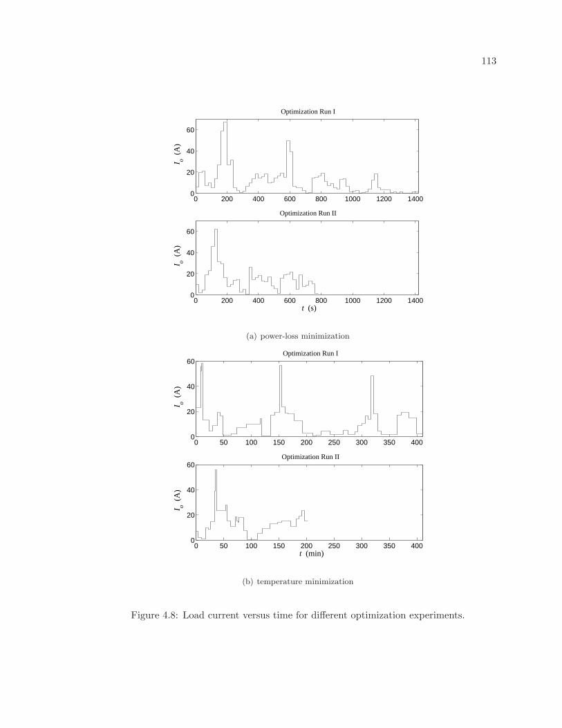
113
0 200 400 600 800 1000 1200 14000
20
40
60
Optimization Run I
Io (
A)
0 200 400 600 800 1000 1200 14000
20
40
60
Optimization Run II
t (s)
Io (
A)
(a) power-loss minimization
0 50 100 150 200 250 300 350 4000
20
40
60 Optimization Run I
Io (
A)
0 50 100 150 200 250 300 350 4000
20
40
60 Optimization Run II
t (min)
Io (
A)
(b) temperature minimization
Figure 4.8: Load current versus time for different optimization experiments.

114
0 10 20 30 40 50 60 70 800
20
40
60
80
100
Io (A)
td,
on (
LSB
= 2
0.83
ns)
0 10 20 30 40 50 60 70 800
5
10
15
Io (A)
td,
on (
LSB
= 2
0.83
ns)
inital conditions Ipower−optimized curve Itemperature−optimized curve Itheoretical DCM curve
inital conditions IIpower−optimized curve IItemperature−optimized curve II
Figure 4.9: Dead-time td,on versus Io curves obtained by power loss and temperature min-imization experiments for different initial conditions. This is a different representation ofthe vertical curves in Fig. 4.6.
0 10 20 30 40 50 60 70 805
10
15
20
Io (A)
td,
off (
LSB
= 2
0.83
ns)
inital conditionspower−optimized curvetemperature−optimized curve
Figure 4.10: Dead-time td,off versus Io curves obtained by power loss and temperatureminimization experiments. This is a different representation of the vertical curves in Fig. 4.7.

115
The td,on curve denoted with ’s, corresponds to optimal DCM operation. Param-
eter td,on is constant for heavy loads, but varies over a wide range for light loads, since
the optimal SR on-time is a strong function of load current in DCM. This is predicted by
equation (4.6) which is also plotted in Fig. 4.9(top), and matches the experimental data
very well. The td,on curve denoted with ∆’s, corresponds to soft-switching behavior.
Fig. 4.11 is a gallery of the switching waveforms of one of the four converter phases,
illustrating behavior at different load currents with optimized SR timing. Oscillogram
(a) shows the converter in CCM at heavy load. Oscillogram (b) illustrates soft-switching
behavior (Io = 10 A, td,on = 7 LSB). Notice the switch-node voltage Vx rising before the
high-side switch Vg1 is turned on, due to negative inductor current charging up the parasitic
switch-node capacitance. It could be the case that for designs with very high switching
frequencies, the soft-switching mode has better performance than DCM, since it reduces
the switching losses. Oscillogram (c) shows DCM operation with gated SR. Oscillograms
(d)–(f) illustrate pulse skipping at very light loads. The converter settles into a limit
cycle consisting of periodic switching bursts, followed by off periods. The average inter-
pulse period is modeled by (4.10). Generally the switching behavior within each burst
is governed by the proportional and derivative terms of the PID control law, while the
alternation between burst and off state is determined by the integral term, which maintains
the output voltage centered at the zero-error ADC bin. Note that the amplitude of the Vo
limit cycle is about two ADC bin sizes (∆Vadc = 11.7 mV), implying switching among the
−1, 0, and +1 LSB error bins, which satisfies the zero average error condition enforced by
the integral PID term.

116
all 5 V/div
Vg1
Vg2
Vx
1 us/div
(a) CCM operation (Io = 35 A).
all 5 V/div
Vg1
Vg2
Vx
1 us/div
(b) Soft-switching (zero-voltage-switching) behavior (Io = 10 A).
1 us/divVg2
Vg1
Vx
all 5 V/div
(c) DCM operation with gated synchronous rectifier (Io = 5 A).
Figure 4.11: Sample switching waveforms in discontinuous and continuous conduction mode.

117
Vo500 us/div20 mV/div
Vx 5 V/div
(d) Pulse skipping (Io = 0.1 A). Periodic behavior at about 560 Hz.
Vo20 mV/div 2 ms/div
5 V/div
Vx
(e) Pulse skipping (Io = 0.01 A); bursts repeat at about 170 Hz.
Vo20 mV/div 50 us/div
Vx
5 V/div
(f) Zoom of single burst in (e); pulse frequency about 94 kHz.
Figure 4.11 (Continued) [Oscilloscope in peak-detect mode to capture narrow pulses.]

118
Fig. 4.12 shows the efficiency of the converter with different number of phases and
operating in different modes. The overall efficiency is not very high, due to the particular
power train used. Informative, however, is the difference in efficiency among the different
modes. The curves corresponding to 4-phase operation in DCM and in soft-switching mode
are the results of the optimization experiment above (using direct power-loss minimization;
the results with temperature minimization are virtually identical). For comparison, the effi-
ciencies associated with forced CCM (td,on = 2 LSB) and with the SR off (td,on = 120 LSB)
for 4-phase operation are plotted as well. These fixed-td,on curves correspond to the two
modes used in controllers which nominally operate in CCM with SR, and turn off the SR
completely at light load (e.g., [17]). By converging into DCM at light-to-medium load
(4 A < Io < 19 A), the SR optimizer improves the efficiency by up to 5% over the better
of the two fixed-td,on alternatives. Below about 3.5A for this configuration it is better to
turn off the SR altogether. In this case, discontinuous-conduction pulse skipping improves
efficiency by 18% compared to nominal CCM operation at 1 A.
Finally, the curves for 2-phase and 1-phase operation in Fig. 4.12 were measured
off-line. Evidently, reducing the number of phases at medium and light loads substantially
decreases the power loss. Below 38 A it is advantageous to run only two phases, and below
17 A single-phase operation is optimal. These transitions among different number of phases
can be straightforwardly scheduled as a function of the load current in a digital controller.
This approach will work well with the adaptive SR control developed above, since the SR
timing is scheduled by the load current as well. Further, to demonstrate the light-load
efficiency improvement with pulse-skipping, an aggressive minimum duty-ratio command
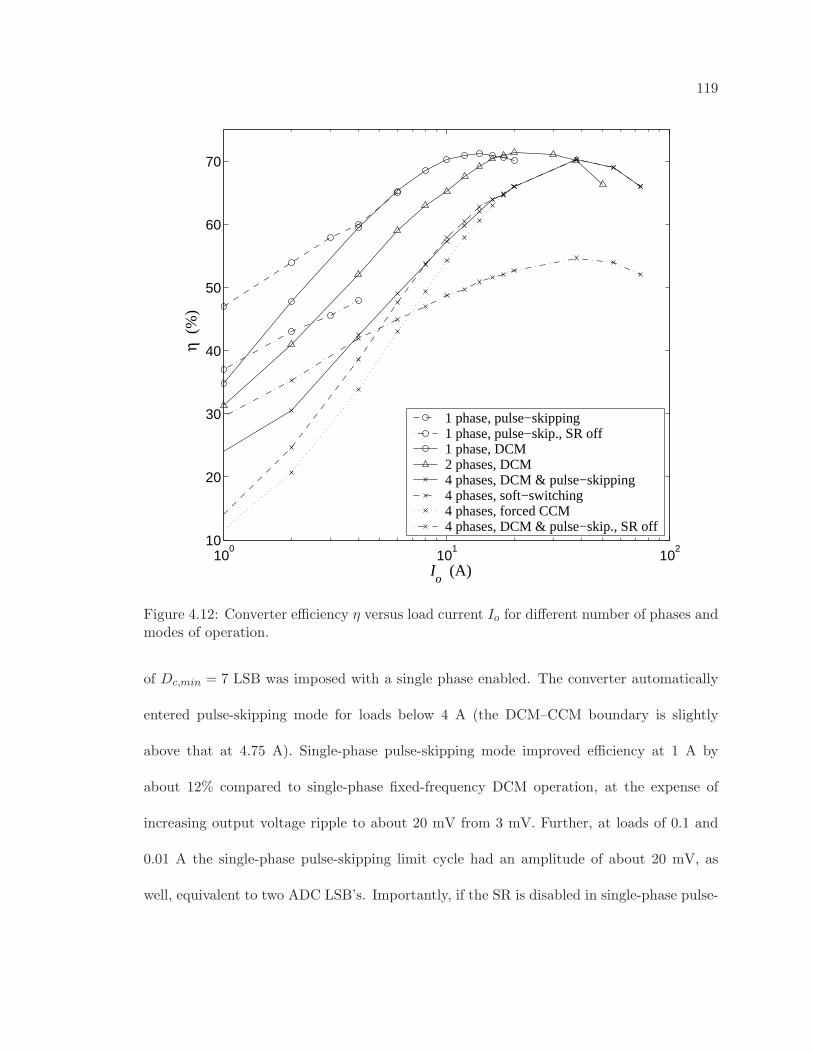
119
100
101
102
10
20
30
40
50
60
70
Io (A)
η (
%)
1 phase, pulse−skipping1 phase, pulse−skip., SR off1 phase, DCM2 phases, DCM4 phases, DCM & pulse−skipping4 phases, soft−switching4 phases, forced CCM4 phases, DCM & pulse−skip., SR off
Figure 4.12: Converter efficiency η versus load current Io for different number of phases andmodes of operation.
of Dc,min = 7 LSB was imposed with a single phase enabled. The converter automatically
entered pulse-skipping mode for loads below 4 A (the DCM–CCM boundary is slightly
above that at 4.75 A). Single-phase pulse-skipping mode improved efficiency at 1 A by
about 12% compared to single-phase fixed-frequency DCM operation, at the expense of
increasing output voltage ripple to about 20 mV from 3 mV. Further, at loads of 0.1 and
0.01 A the single-phase pulse-skipping limit cycle had an amplitude of about 20 mV, as
well, equivalent to two ADC LSB’s. Importantly, if the SR is disabled in single-phase pulse-

120
skipping the efficiency drops by about 10% due to the relatively large on-time resulting in
long SR conduction. Therefore, in this case it is beneficial to gate the SR in pulse-skipping.
4.5 Conclusion
This chapter developed a multi-mode control paradigm which operates the buck
converter in continuous and discontinuous conduction mode, at heavy and light load, re-
spectively, and in variable pulse-skipping mode at very light loads. The transition between
continuous and discontinuous conduction is managed by scheduling the synchronous recti-
fier timing as a function of the load current, and optimizing it on-line so as to minimize
power loss. The transition to pulse skipping is effected with a simple limit on the minimum
duty-ratio command. In an experimental 100 W 4-phase buck converter the adaptive algo-
rithm successfully optimized the synchronous rectifier timing over the full load range, using
alternately direct power loss and temperature minimization. This resulted in up to 5% ef-
ficiency improvement in discontinuous conduction mode. Further, pulse skipping improved
the efficiency by 18% at very light load.
Perturbations at 100 and 200 Hz were used for the direct power loss minimization,
resulting in very fast convergence of the algorithm. Slower perturbations of 0.2 and 0.4
Hz were applied in the temperature minimization experiment, due to the slow response of
the thermal sensors used in the setup. In practical implementations, temperature sensors
could be integrated on the MOSFET switch dies, yielding fast thermal response, in which
case high-frequency perturbations could be used. Integrating temperature sensors in power
MOSFET’s would enable other functionality, such as fault control, and phase-current bal-

121
ancing based on adaptive thermal equalization among the phase legs, which could enhance
the converter reliability [61, 62]. Integrated temperature sensing can be accomplished with
a single diode, which has a temperature coefficient of −2 mV/C [33, Ch. 1], as is done in
some modern high-performance microprocessors (e.g., [78].
In Section 4.4 it was pointed out that the power loss signal was divided by Io before
being used in the gradient estimator. This approach successfully reduced both gradient-
estimator disturbances resulting from load changes, and adaptive-loop gain variation. It
could be further improved by normalizing the power loss (or temperature) by I2o in CCM,
and by I3/2o in DCM, since these terms factor in the corresponding power loss equation
(4.2) and (4.7), respectively. In should be noted that the adaptive nature of the power
optimization algorithm obviates the need for accurate measurement or estimation of the
load current. As long as the scheduling quantity is a monotone increasing function of
the load current, the algorithm can work. In fact, other quantities related to the load
current, such as the inductor current or even the input current could be used for scheduling.
Since the input current depends on the power loss, which is being optimized, using it as a
scheduling variable could somewhat complicate the dynamics of the problem. However, it
seems that with appropriate controller time scale separation this issue would be manageable.
In general, it would be interesting to study more rigorously the convergence properties of the
SR adaptation algorithm with respect to load current dynamics and small, local, power-
loss minima. A good starting point for theoretical stability studies of extremum-seeking
methods is the work in [41, 40, 96, 5, 11].
It was seen in Fig. 4.11(d)–(f) that at very light loads the converter exhibits

122
pulse-skipping behavior characterized by bursts of switching, followed by periods of no
switching. In existing applications, dedicated circuitry is required to implement ”burst-
mode” control, and switch between it and fixed-frequency operation (e.g., [27]). In contrast,
the digital controller presented here automatically enters burst-mode operation at light loads
by imposing a minimum duty ratio limit, without modifications of the controller structure.
This behavior is closely related to the limit cycling described in Section 3.5. By enforcing a
minimum duty-ratio we effectively decrease the DPWM resolution at light loads, violating
no-limit-cycle condition (3.3), and thus effecting a limit cycle. The amplitude of the pulse-
skipping limit cycle depends on the resolution of the output-voltage ADC, and is typically
about two ADC LSB’s. The limit-cycle characteristics can further be controlled by adjusting
the PID parameters at light load.
Finally, in the text it was suggested that scheduling other parameters, besides
the synchronous-rectifier timing, as a function of the load current can result in additional
performance improvements. For example, using an array of feedback integrators spanning
the load range can enhance the transient response, as discussed in Section 4.3.1. Further,
Fig. 4.12 demonstrated that adjusting the number of phases on-line as a function of the load
current could effect substantial efficiency increase. For instance, disabling three of the four
phases and applying aggressive pulse-skipping at light load can increase efficiency by some
17%. These techniques were not implemented in the experimental multi-mode controller,
and present an exciting opportunity for future study.

123
Chapter 5
Contributions of Thesis and
Suggestions for Future Research
5.1 Contributions of Thesis
A summary of the contributions of this thesis contrasted to previous work is given
below:
Generalized Output-Impedance Control of Voltage Regulators Chapter 2 developed
a consistent framework, covering both feedback and feedforward approaches, for load-
line regulation which does not require the closed-loop output impedance to equal the
output capacitor ESR. This framework covers capacitors technologies with a wide
range of ESR times constants, such as electrolytic and ceramic capacitors. Previous
work (e.g., [82, 116, 115]) had concentrated on the case when the output capacitor
ESR is equal to the closed-loop output impedance.
124
Load-Line Control with Load-Current Feedforward In Section 2.4 it was demon-
strated that load-current feedforward can extend the useful converter bandwidth with-
out increasing the switching frequency, since feedforward is not subject to feedback
stability constraints. This approach can effect a reduction of the number of output
capacitors in microprocessor VR’s, for example. In contrast, the bandwidth of feed-
back load-line control is limited to below the switching frequency [116, 115]. Previous
work on microprocessor VR control had mostly focused on feedback approaches (e.g.,
[82, 116, 115]), or suggested that load-current feedforward does not outperform fast
feedback methods [81]. Further, previous work on load-current feedforward [83, 81]
was in the context of current-mode control with stiff voltage regulation. The feedfor-
ward control law, which is unity in this case, was derived from large-signal analysis. In
contrast, Section 2.4 developed dynamic, small-signal load-current feedforward laws
for load-line regulation with both current-mode and voltage-mode control.
Extended Critical Capacitance Analysis In Section 2.5 a large-signal critical capac-
itance constraint was derived, extending the analysis in [82, 81]. The critical ca-
pacitance expression allows the load-line impedance value to differ from that of the
output capacitor ESR, and accounts for controller delay and load-current slew rate.
The critical capacitance result allows for inductor value selection both below and
above the critical inductance value discussed in [77, 103, 116]. The critical capac-
itance framework appears more appropriate since the inductance value is typically
chosen considering inductor current ripple, and the size of the output capacitor is
determined subsequently based on output voltage ripple and transient constraints.

125
Efficient ADC and DPWM Architectures In Chapter 3 novel approaches to high-
resolution, power-efficient, small-area ADC and DPWM blocks were proposed. A
”window” ADC architecture quantizes the output voltage only in a small window
around the reference voltage (Section 3.2), resulting in better implementation area
and efficiency compared to ADC’s which quantize a wide voltage range. Further, digi-
tal dither was introduced to boost the resolution of DPWM modules, without power or
area penalties (Section 3.6). In contrast to sigma-delta dither approaches [48, 66, 49],
the proposed programmed-dither method uses pre-computed dither sequences which
minimize the output-voltage ripple.
Conditions for Limit-Cycle Elimination It had previously been observed that closed-
loop operation of a digitally-controlled power converter could result in limit cycling
behavior due to the quantization in the feedback path [107]. To address this problem,
conditions on the quantizer resolution and the feedback control law for limit-cycle
elimination were developed in Section 3.5.
Load-Scheduled Loss-Minimizing Synchronous-Rectifier Control A method for di-
rect control of synchronous rectifiers as a function of the load current is developed
in Chapter 4. The function relating the synchronous rectifier timing to the load cur-
rent is obtained on-line via loss-minimizing multi-parameter adaptation. Only low-
bandwidth measurements of the load current and a power-loss-related quantity (such
as input current or temperature) are required, in contrast to common synchronous
rectifier control techniques [39, 91, 3, 42, 51]. Further, compared to alternative loss-
minimizing approaches [2, 117], this method has superior adjustment speed and ro-

126
bustness to transients, and can simultaneously optimize multiple parameters. Finally,
as discussed in Section 4.3.1, a similar adaptive scheduling approach can be used
to rapidly adjust the duty ratio in DCM, providing fast load-transient response in
multi-mode operation.
Automatic Multi-Mode Buck Operation The loss-minimizing synchronous-rectifier con-
trol accomplishes an automatic, optimal transition to DCM at light loads. Further, by
imposing a minimum duty-ratio the converter will automatically enter pulse-skipping
mode at very light loads, as shown in Chapter 4. Thus, the same controller structure
could be used in both fixed-frequency PWM and variable-frequency pulse-skipping
modes. This is in contrast to typical multi-mode designs in which a separate control
law is used for light-load variable frequency operation (e.g., [27, 79, 110]). This multi-
mode control strategy allows for efficient operation of the buck converter over a wide
load range.
5.2 Suggestions for Future Research
Some ideas of how the work in this thesis can be extended were already discussed
in the text. Here we attempt to summarize the more important suggestions, and outline
directions for future work:
5.2.1 Load Current Estimators
The load-line control methods described in Chapter 2 rely on accurate estimation of
the load current. Passive estimation methods such as the ones described in Section 2.7.3 rely

127
on matching of the estimator parameters to these of the power train, and are thus sensitive
to component tolerances, temperature, and drift. More robust, adaptive estimators could be
developed. For example, input-current measurements of microprocessor VR’s are relatively
easy to implement due to the low nominal duty ratio. The input-current measurement
could be used to tune a passive load current estimator such as the one in Section 2.7.3, or
an estimator based on trace or package resistance (e.g., [78]). Estimation techniques for
power electronic circuits are discussed in [37], for example.
5.2.2 Adaptive Load-Current Feedforward
The load-line regulation method using load-current feedforward discussed in Sec-
tion 2.4 can provide very fast converter response, however is is sensitive to mismatches
between the power train parameters and the nominal values used in the feedforward control
law. For example, in a voltage-mode controller implementation, which is typical for mi-
croprocessor VR’s, the feedforward control law (2.22) uses the nominal values of the total
inductance and output capacitance, which could differ from the actual values. This problem
can be addressed by adaptively tuning the feedforward law. For example, if the feedforward
is perfect, the feedback error signal will always be zero. Hence, feedforward tuning could
be based on minimizing the error signal over time. Relevant discussion of adaptive control
can be found in [8, 89], for example.
5.2.3 Multi-Mode Control
Over its full load range the switching power converter could span a number of
modes as described in Section 4.2. Due to the different converter behavior, it is generally

128
appropriate to adjust some of the controller parameters in the different modes. A general
framework promoted in this thesis is to schedule these parameters as a function of the load
current, and to estimate an optimal value of this function either off-line or on-line. This
approach was demonstrated with loss-minimizing synchronous rectifier control in Chapter
4. In the same chapter it was shown that a similar approach could provide fast integrator
adjustment in all modes. It was also demonstrated that adjusting the number of active
phases as a function of the load could provide high efficiency over a wide load range. The
integrator scheduling and the phase scaling were not implemented experimentally in this
work, and merit future study.
Further, the load-current feedforward control laws in Section 2.4 were derived for
CCM. In CCM the control-to-output transfer function of the buck converter is second-
order and is independent of the load current. In DCM, however, the control-to-output
transfer function is first-order and is dependent on the load [28, Ch. 11]. Thus, it would be
appropriate to adjust the feedforward law as a function of the load current in DCM.
Similarly, due to the changing control-to-output transfer function between DCM
and CCM, the PID control law coefficients in (3.1) may have to be adjusted to ensure good
closed-loop performance. Further, in the pulse-skipping mode the limit-cycle determining
the pulse sequences depends on the PID coefficients. Thus, it could be appropriate to
adjust the PID law as a function of the load current, as well. This approach is referred to
as gain-scheduling, and is discussed in [8, Ch. 9], for example.
129
5.2.4 PID Self-Tuning
A related issue is that the PID control law is typically designed based on the
nominal power train parameters. Due to component tolerance, ambient conditions, and
aging these parameters may change, possibly resulting in degraded closed-loop performance.
A digital controller can perform on-line PID tuning to overcome this problem. In the
extreme case, the controller may start with little or no a priori knowledge of the power train
parameters, and the controller could carry out experiments to identify these parameters and
assign appropriate PID coefficients. This could eliminate the need for PID customization
and the associated human expertise.
System identification and PID tuning can be carried out during an off-line cali-
bration routine, during the converter power-up sequence, or during normal operation. For
example, when the host system is turned on, the power converter typically underdoes a soft-
start sequence in which the output voltage is gradually ramped up to the reference voltage.
During the start-up transient the host system is not operational yet, and the digital power
controller can carry out both open-loop and closed-loop experiments to characterize the
power train parameters. PID coefficients can be computed based on this parameter esti-
mates and a given PID design method. Under normal, regulated operation, closed-loop
experiments can be carried out to further fine-tune the PID control law. The system can
be driven into a self-oscillation with an acceptable amplitude, or a perturbation can be
injected in the control signal. The latter has been used to estimate on-line the transfer
characteristic of a power converter [54, 55]. Alternatively, natural disturbances such as load
current transients can be used to estimate the converter parameters. Discussion of PID

130
controller self-tuning can be found in [7, 8], for example. An expansive reference review of
modern PID controller design is given in [44].

131
Bibliography
[1] J. Abu-Qahouq, H. Mao, and I. Batarseh. Multiphase voltage-mode hysteretic con-
trolled DC–DC converter with novel current sharing. IEEE Trans. Power Electron.,
19(6):1397–1407, November 2004.
[2] J. A. Abu-Qahouq, H. Mao, H. J. Al-Atrash, and I. Batarseh. Maximum efficiency
point tracking (MEPT) method and dead time control. In Proc. IEEE Power Electron.
Spec. Conf., volume 5, pages 3700–3706, 2004.
[3] B. Acker, C. R. Sullivan, and S. R. Sanders. Synchronous rectification with adaptive
timing control. In Proc. IEEE Power Electron. Spec. Conf., volume 1, pages 88–95,
1995.
[4] B. Arbetter and D. Maksimovic. Control method for low-voltage DC power supply
in battery-powered systems with power management. In Proc. IEEE Power Electron.
Spec. Conf., volume 2, pages 1198–1204, 1997.
[5] K. B. Ariyur and M. Krstic. Analysis and design of multivariable extremum seeking.
In Proc. American Control Conf., pages 2903–2908, May 2002.
[6] S. Ashley. Power–thrifty PCs. Scientific American, 290(6):31–32, June 2004.

132
[7] K. J. Astrom and T. Hagglund. PID Controllers: Theory, Design, and Tuning. Instr.
Soc. of America, Research Triangle Park, North Carolina, second edition, 1995.
[8] K. J. Astrom and B. Wittenmark. Adaptive Control. Addison Wesley Longman,
second edition, 1995.
[9] S. Banerjee and G. C. Verghese (Editors). Nonlinear Phenomena in Power Electronics:
Attractors, Bifurcations, Chaos, and Nonlinear Control. New York: IEEE Press, 2001.
[10] A. Barrado, R. Vazquez, E. Olıas, A. Lazaro, and J. Pleite. Theoretical study and im-
plementation of a fast transient response power supply. IEEE Trans. Power Electron.,
19(4):1003–1009, July 2004.
[11] D. P. Bertsekas. Nonlinear Programming. Belmont, MA: Athena Scientific, second
edition, 1999.
[12] T. D. Burd, T. A. Pering, A. J. Stratakos, and R. W. Brodersen. A dynamic voltage
scaled microprocessor system. IEEE JSSC, 35(11):1571–1580, November 2000.
[13] C. Calwell and A. Mansoor. AC-DC server power supplies: Making the leap to higher
efficiency. In IEEE Appl. Power Electron. Conf., pages 155–158, 2005.
[14] S. Canter and R. Lenk. Stabilized power converter having quantized duty cycle.
United States Patent Number 5,594,324, January 1997.
[15] B. Carroll. Cost-effective digital control for core power. In Darnell Digital Power
Forum, volume CD-ROM, September 2004.
133
[16] A. P. Chandrakasan and R. W. Brodersen. Low Power Digital CMOS Design. Boston,
MA: Kluwer Academic Publishers, 1995.
[17] G. Chinn, S. Desai, E. DiStefano, K. Ravichandran, and S. Thakkar. Mobile PC
platforms enabled with Intel CentrinoTM mobile technology. Intel Tech. J., 7(2), May
2003.
[18] W. D. Collins. Digital technology invades power supply control market (power man-
agement components topical report). [Online]. Available: http://www.isuppli.com,
2003.
[19] Intel Corp. Voltage Regulator–Down (VRD) 10.1. [Online]. Available:
http://developer.intel.com/design/Pentium4/documentation.htm, July 2004.
[20] Intel Corp. Moore’s Law. [Online]. Available:
http://www.intel.com/research/silicon/mooreslaw.htm, 2005.
[21] International Rectifier Corp. IR3081: XPHASETM VR 10.0 control IC. Data Sheet,
September 2003.
[22] A. P. Dancy, R. Amirtharajah, and A. P. Chandrakasan. High-efficiency multiple-
output DC-DC conversion for low-voltage systems. IEEE Trans. VLSI Sys., 8(3):252–
263, June 2000.
[23] A. P. Dancy and A. P. Chandrakasan. Ultra low power control circuits for PWM
converters. In Proc. IEEE Power Electron. Spec. Conf., volume 1, pages 21–27, 1997.
[24] H. Deng, A. Q. Huang, and Y. Ma. Design of a monolithic high frequency fast
134
transient buck for portable application. In Proc. IEEE Power Electron. Spec. Conf.,
pages 4448–4452, 2004.
[25] I. Deslauriers, N. Avdiu, and B. T. Ooi. Naturally sampled triangle carrier PWM
bandwidth limit and output spectrum. IEEE Trans. Power Electron., 20(1):100–106,
January 2005.
[26] Y. Duan and H. Jin. Digital controller design for switching mode power converters.
In Proc. IEEE Applied Power Electron. Conf., volume 2, pages 967–73, 1999.
[27] D. Eagar and S. Pietkiewicz. Applications of the LT1300 and LT1301 micropower
DC/DC converters. Application Note 59, Linear Technology, January 1994.
[28] R. W. Erickson and D. Maksimovic. Fundamentals of Power Electronics. Kluver
Academic Publishers, second edition, 2001.
[29] International Technology Roadmap for Semiconductors. Executive summary. [Online].
Available: http://public.itrs.net, 2003.
[30] International Technology Roadmap for Semiconductors. Update. [Online]. Available:
http://public.itrs.net, 2004.
[31] G. F. Franklin, J. D. Powell, and M. Workman. Digital Control of Dynamic Systems.
Menlo Park: Addison-Wesley, third edition, 1998.
[32] A. Gelb and W. E. Vander Velde. Multiple-Input Describing Functions and Nonlinear
System Design. New York: McGraw-Hill, 1968.

135
[33] P. R. Gray, P. J. Hurst, S. H. Lewis, and R. G. Meyer. Analysis and Design of Analog
Integrated Circuits. New York: Wiley, fourth edition, 2001.
[34] Darnell Group. Emerging markets in digital power electronics: Component,
converter and system level opportunities (industry study). [Online]. Available:
http://www.darnell.com/services/studies.stm, 2005.
[35] Silicon Laboratories Inc. Si8250: Digital power controller. Data Sheet, April 2005.
[36] Texas Instruments Inc. TMDSDPS2000: Digital power solutions development kit.
Data Sheet, December 2002.
[37] L. A. Kamas and S. R. Sanders. Parameter and state estimation in power electronic
circuits. IEEE Trans. Circ. Sys. I: Fund. Theory Appl., 40(12):920–928, December
1993.
[38] J. W. Kimball. Application of nonlinear control techniques in low voltage DC-DC
converters. M.S. thesis, University of Illinois, 1996.
[39] P. T. Krein and R. M. Bass. Autonomous control techniques for high-performance
switches. IEEE Trans. Ind. Electron., 39(3):215–222, June 1992.
[40] M. Krstic. Performance improvement and limitations in extremum seeking control.
Syst. Contr. Lett., 39:313–326, 2000.
[41] M. Krstic and H.-H. Wang. Stability of extremum seeking feedback for general non-
linear dynamic systems. Automatica, 36:595–601, 2000.

136
[42] W. Lau and S. R. Sanders. An integrated controller for a high frequency buck con-
verter. In Proc. IEEE Power Electron. Spec. Conf., volume 1, pages 246–254, 1997.
[43] F. C. Lee. High frequency solutions for 12 V VR. In Intel Tech. Symp., September
2003.
[44] M. Lelic and Z. Gajic. A reference guide to PID controllers in the nineties. In Proc.
IFAC Digital Control: Past, Present and Future, pages 69–78, 2000.
[45] Jieli Li, A. Stratakos, A. Schultz, and C. R. Sullivan. Using coupled inductors to
enhance transient performance of multi-phase buck converters. In Proc. IEEE Applied
Power Electron. Conf., volume 2, pages 1289–1293, 2004.
[46] Jieli Li, C. R. Sullivan, and A. Schultz. Coupled-inductor design optimization for
fast-response low-voltage DC–DC converters. In Proc. IEEE Applied Power Electron.
Conf., volume 2, pages 817–823, 2002.
[47] D. L. Logue and P. T. Krein. Optimization of power electronic systems using rip-
ple correlation control: A dynamic programming approach. In Proc. IEEE Power
Electron. Spec. Conf., volume 2, pages 459–464, 2001.
[48] G. Luckjiff, I. Dobson, and D. Divan. Interpolative sigma delta modulators for high
frequency power electronic applications. In Proc. IEEE Power Electron. Spec. Conf.,
volume 1, pages 444–449, 1995.
[49] Z. Lukic, K. Wang, and A. Prodic. High-frequency digital controller for DC-DC
converter based on multi-bit Σ-∆ pulse-width modulation. In Proc. IEEE Applied
Power Electron. Conf., pages 35–40, 2005.

137
[50] P. Mahajan, R. Nair, V. Wakharkar, J. Swan, J. Tang, and G. Vandentop. Emerging
directions for packaging technologies. Intel Tech. J., 6(2), May 2002.
[51] S. Mappus. Predicitve gate driveTM boosts synchronous DC/DC power converter
efficiency. Application Report SLUA281, Texas Instruments Inc., April 2003.
[52] T. W. Martin and S. S. Ang. Digital control of switching converters. In Proc. IEEE
Internat. Symp. on Indust. Electron., volume 2, pages 480–4, 1995.
[53] G. J. Mehas, K. D. Coonley, and C. R. Sullivan. Converter and inductor design for
fast-response microprocessor power delivery. In Proc. IEEE Power Electron. Spec.
Conf., volume 3, pages 1621–1626, 2000.
[54] B. Miao, R. Zane, and D. Maksimovic. A modified cross-correlation method for system
identification of power converters with digital control. In Proc. IEEE Power Electron.
Spec. Conf., pages 3728–3733, 2004.
[55] B. Miao, R. Zane, and D. Maksimovic. Practical on-line identification of power con-
verter dynamic responses. In Proc. IEEE Appl. Power Electron. Conf., pages 57–62,
2005.
[56] P. Midya and K. Haddad. Two sided latched pulse width modulation control. In Proc.
IEEE Power Electron. Spec. Conf., pages 628–633, 2000.
[57] P. Midya, P. T. Krein, and M. F. Greuel. Sensorless current mode control—an
observer-based technique for DC–DC converters. IEEE Trans. Power Electron.,
16(4):522–526, July 2001.

138
[58] P. Midya, P. T. Krein, R. J. Turnbull, R. Reppa, and J. Kimball. Dynamic maximum
power point tracker for photovoltaic applications. In Proc. IEEE Power Electron.
Spec. Conf., volume 2, pages 1710–1716, 1996.
[59] Z. Moussaoui. Digital vs. analog power control for microprocessor core regulation. In
Darnell Digital Power Forum, volume CD-ROM, September 2004.
[60] B. Murmann and B. E. Boser. Digitally Assisted Pipeline ADCs: Theory and Imple-
mentation. Kluwer Academic Publishers, 2004.
[61] C. Nesgaard and M. A. E. Andersen. Efficiency improvement in redundant power
systems by means of thermal load sharing. In Proc. IEEE Applied Power Electron.
Conf., volume 1, pages 433–439, 2004.
[62] C. Nesgaard and M. A. E. Andersen. Optimized load sharing control by means of
thermal reliability management. In Proc. IEEE Power Electron. Spec. Conf., pages
4901–4906, 2004.
[63] C. Nesgaard, M. A. E. Andersen, and N. Nielsen. Digitally controlled converter with
dynamic change of control law and power throughput. In Proc. IEEE Power Electron.
Spec. Conf., pages 1163–1168, 2003.
[64] S. R. Norsworthy, R. Schreier, and G. C. Temes. Delta-Sigma Data Converters. New
York: IEEE Press, 1996.
[65] Y. Panov and M. Jovanovic. Design considerations for 12-V/1.5-V, 50-A voltage
regulation modules. IEEE Trans. Power Electron., 16(6):776–783, November 2001.

139
[66] C. Pascual, Z. Song, P. T. Krein, D. V. Sarwate, P. Midya, and W. J. Roeckner. High-
fidelity PWM inverter for digital audio amplification: Spectral analysis, real-time DSP
implementation, and results. IEEE Trans. Power Electron., 18(1-II):473–485, January
2003.
[67] B. J. Patella, A. Prodic, A. Zirger, and D. Maksimovic. High-frequency digital PWM
controller IC for DC-DC converters. IEEE Trans. Power Electron., 18(1-II):438–446,
January 2003.
[68] H. Peng, D. Maksimovic, A. Prodic, and E. Alarcon. Modeling of quantization effects
in digitally controlled DC-DC converters. In Proc. IEEE Power Electron. Spec. Conf.,
pages 4312–4318, 2004.
[69] L. Peng, X. Kong, Y. Kang, and J. Chen. A novel PWM technique in digital control
and its application to an improved DC/DC converter. In Proc. IEEE Power Electron.
Spec. Conf., volume 1, pages 254–259, 2001.
[70] A. V. Peterchev. Digital control of PWM converters: Analysis and application to
voltage regulation modules. M.S. thesis, University of California, Berkeley, May 2002.
[71] A. V. Peterchev and S. R. Sanders. Quantization resolution and limit cycling in
digitally controlled PWM converters. In Proc. IEEE Power Electron. Spec. Conf.,
volume 2, pages 465–471, 2001.
[72] A. V. Peterchev and S. R. Sanders. Low conversion ratio VRM design. In Proc. IEEE
Power Electron. Spec. Conf., volume 4, pages 1571–1575, 2002.

140
[73] A. V. Peterchev and S. R. Sanders. Quantization resolution and limit cycling in
digitally controlled PWM converters. IEEE Trans. Power Electron., 18(1-II):301–
308, January 2003.
[74] A. V. Peterchev and S. R. Sanders. Design of ceramic-capacitor VRM’s with estimated
load current feedforward. In Proc. IEEE Power Electron. Spec. Conf., pages 4325–
4332, 2004.
[75] A. V. Peterchev and S. R. Sanders. Design of VRM/VRD with ceramic output capac-
itors with true estimated load current feed forward. In Intel Tech. Symp., September
2004.
[76] A. V. Peterchev and S. R. Sanders. Digital loss-minimizing multi-mode synchronous
buck converter control. In Proc. IEEE Power Electron. Spec. Conf., pages 3694–3699,
2004.
[77] A. V. Peterchev, J. Xiao, and S. R. Sanders. Architecture and IC implementation of
a digital VRM controller. IEEE Trans. Power Electron., 18(1-II):356–364, January
2003.
[78] C. Poirier, R. McGowen, C. Bostak, and S. Naffziger. Power and temperature control
on a 90nm Itanium-family processor. In IEEE Int. Solid-State Circ. Conf. Dig. Tech.
Papers, volume 1, pages 304–305, 2005.
[79] A. Prodic and D. Maksimovic. Control method for low-voltage DC power supply in
battery-powered systems with power management. In IEEE Comput. Power Electron.
Workshop, pages 123–128, 2000.
141
[80] Y. Qiu, M. Xu, K. Yao, J. Sun, and F. C. Lee. The multi-frequency small-signal
model for buck and multiphase interleaving buck converters. In Proc. IEEE Applied
Power Electron. Conf., pages 392–398, 2005.
[81] R. Redl. DC/DC converters for microprocessor core power supplies. In Lecture Notes
for Power Management, December 1999. Seminar organized by MEAD Microelec-
tronics, Inc.
[82] R. Redl, B. P. Erisman, and Z. Zansky. Optimizing the load transient response of
the buck converter. In Proc. IEEE Applied Power Electron. Conf., volume 1, pages
170–176, 1998.
[83] R. Redl and N. O. Sokal. Near-optimum dynamic regulation of DC–DC converters
using feed-forward of output current and input voltage with current-mode control.
IEEE Trans. Power Electron., PE-1(3):181–192, July 1986.
[84] Yuancheng Ren, M. Xu, K. Yao, Y. Meng, and F. C. Lee. Two-stage approach for
12-V VR. IEEE Trans. Power Electron., 19(6):1498–1506, November 2004.
[85] N. Rossetti and S. R. Sanders. Valley design techniques outperform peak current
mode approach for CPU supplies. PCIM Power Electronic Systems, July 2001.
[86] S. R. Sanders, A. V. Peterchev, and J. Xiao. Digital controller for an interleaved
voltage regulator. In Intel Tech. Symp., September 2000.
[87] S. R. Sanders, A. V. Peterchev, J. Xiao, and J. Zhang. Digital PWM IC control
technology and issues. In Darnell Digital Power Forum, volume CD-ROM, September
2004.

142
[88] Fairchild Semiconductor. FAN5093: Two phase interleaved synchronous buck con-
verter for VRM 9.x applications. Data Sheet, March 2003.
[89] J.-J. E. Slotine and W. Li. Applied Nonlinear Control. New Jersey: Prentice-Hall,
1991.
[90] E. Stanford. Power technology roadmap for microprocessor voltage regulators. In
IEEE Applied Power Electron. Conf. (Spec. Present. Session), volume SP1.1, 2004.
[Online]. Available: http://www.apec-conf.org.
[91] A. J. Stratakos, S. R. Sanders, and R. W. Brodersen. A low-voltage CMOS DC-DC
conveter for a portable battery-operated system. In Proc. IEEE Power Electron. Spec.
Conf., volume 1, pages 619–626, 1994.
[92] C. R. Sullivan and A. M. Kern. Capacitors with fast current switching require dis-
tributed models. In Proc. IEEE Power Electron. Spec. Conf., volume 3, pages 1497–
1503, 2001.
[93] C. R. Sullivan, Y. Sun, and A. M. Kern. Improved distributed model for capacitors in
high-performance packages. In Proc. IEEE Applied Power Electron. Conf., volume 2,
pages 969–976, 2002.
[94] C. Varga. Novel controller for next generation portable CPU power. In Intel Tech.
Symp., September 2004.
[95] G. C. Verghese, C. A. Bruzos, and K. N. Mahabir. Averaged and sampled-data
models for current mode control: A reexamination. In Proc. IEEE Power Electron.
Spec. Conf., pages 484–491, 1989.

143
[96] G. C. Walsh. On the application of multi-parameter extremum seeking control. In
Proc. American Control Conference, volume 1, pages 411–415, 2000.
[97] A. C. Wang and S. R. Sanders. Programmed pulsewidth modulated waveforms for
electromagnetic interference mitigation in DC-DC converters. IEEE Trans. Power
Electron., 8(4):596–605, October 1993.
[98] T. G. Wang, X. Zhou, and F. C. Lee. A low voltage high efficiency and high power
density DC/DC converter. In Proc. IEEE Power Electron. Spec. Conf., volume 1,
pages 240–245, 1997.
[99] G.-Y. Wei and M. Horowitz. A low power switching power supply for self-clocked
systems. In IEEE Int. Symp. Low Power Electron. Design Dig. Tech. Papers, pages
313–317, August 1996.
[100] G.-Y. Wei and M. Horowitz. A fully digital, energy-efficient, adaptive power-supply
regulator. IEEE J. Solid-State Circ., 34(4):520–8, April 1999.
[101] G.-Y. Wei, J. Kim, D. Liu, S. Sidiropoulos, and M. Horowitz. A variable-frequency
parallel I/O interface with adaptive power-supply regulation. IEEE J. Solid-State
Circ., 35(11):1600–1610, November 2000.
[102] J. Wei, P. Xu, and F. C. Lee. A high efficiency topology for 12 V VRM push-pull buck
and its integrated magnetics implementation. In Proc. IEEE Appl. Power Electron.
Conf., pages 679–685, 2002.
[103] Pit-Leong Wong, F. C. Lee, P. Xu, and K. Yao. Critical inductance in voltage regulator
modules. IEEE Trans. Power Electron., 17(4):485–492, July 2002.
144
[104] Pit-Leong Wong, P. Xu, P. Yang, and F. C. Lee. Performance improvements of
interleaving vrms with coupling inductors. IEEE Trans. Power Electron., 16(4):499–
507, July 2001.
[105] CPU World. Microprocessors/central processing units (CPU) families. [Online]. Avail-
able: http://www.cpu-world.com/CPUs/CPU.html, 2005.
[106] A. M. Wu and S. R. Sanders. An active clamp circuit for voltage regulation module
(VRM) applications. IEEE Trans. Power Electron., 16(5):623–634, September 2001.
[107] A. M. Wu, J. Xiao, D. Markovic, and S. R. Sanders. Digital PWM control: application
in voltage regulation modules. In Proc. IEEE Power Electron. Spec. Conf., volume 1,
pages 77–83, 1999.
[108] J. Xiao, A. V. Peterchev, and S. R. Sanders. Architecture and IC implementation
of a digital VRM controller. In Proc. IEEE Power Electron. Spec. Conf., volume 1,
pages 38–47, 2001.
[109] J. Xiao, A. V. Peterchev, J. Zhang, and S. R. Sanders. A 4 µa quiescent-current dual-
mode buck converter IC for cellular phone applications. In IEEE Int. Solid-State Circ.
Conf. Dig. Tech. Papers, volume 1, pages 280–281, 2004.
[110] J. Xiao, A. V. Peterchev, J. Zhang, and S. R. Sanders. A 4-µa quiescent-current dual-
mode digitally controlled buck converter IC for cellular phone applications. IEEE J.
Solid-State Circ., 39(12):2342–2348, December 2004.
[111] J. Xiao, A. V. Peterchev, J. Zhang, and S. R. Sanders. An ultra-low-power digitally-

145
controlled buck converter IC for cellular phone applications. In Proc. IEEE Appl.
Power Electron. Conf., volume 1, pages 383–391, 2004.
[112] P. Xu, J. Wei, and F. C. Lee. The active-clamp coupled-buck converter—a novel
high efficiency voltage regulator module. In Proc. IEEE Appl. Power Electron. Conf.,
pages 252–257, 2001.
[113] Kaiwei Yao. High-Frequency and High-Performance VRM Design for the Next Gen-
erations of Processors. PhD thesis, Virg. Polytech. Inst. and State Univ., 2004.
[114] Kaiwei Yao, Y. Meng, and F. C. Lee. A novel winding coupled buck converter for
high step-down DC/DC conversion. In Proc. IEEE Power Electron. Spec. Conf., pages
651–656, 2002.
[115] Kaiwei Yao, Y. Ren, and F. C. Lee. Critical bandwidth for the load transient re-
sponse of voltage regulator modules. IEEE Trans. Power Electron., 19(6):1454–1461,
November 2004.
[116] Kaiwei Yao, M. Xu, Y. Meng, and F. C. Lee. Design considerations for VRM transient
response based on the output impedance. IEEE Trans. Power Electron., 18(6):1270–
1277, November 2003.
[117] V. Yousefzadeh and D. Maksimovic. Sensorless optimization of dead times in DC-DC
converters with synchronous rectification. In Proc. IEEE Applied Power Electron.
Conf., pages 911–917, 2005.
[118] Xin Zhang and A. Q. Huang. Impacts of transient voltage clamp on CPU power
delivery. In Proc. IEEE Power Electron. Spec. Conf., pages 629–632, 2004.

146
[119] Xin Zhang, G. Yao, and A. Q. Huang. A novel VRM control with direct load current
feedback. In Proc. IEEE Applied Power Electron. Conf., volume 1, pages 267–271,
2004.
[120] Y. Zhang, R. Zane, A. Prodic, R. Erickson, and D. Maksimovic. Online calibration of
MOSFET on-state resistance for precise current sensing. IEEE Power Electron. Lett.,
2(3):100–103, September 2004.
[121] Xunwei Zhou, P.-L. Wong, P. Xu, F. C. Lee, and A. Q. Huang. Investigation of
candidate VRM topologies for future microprocessors. IEEE Trans. Power Electron.,
15(6):1172–1182, November 2000.

147
Appendix A
PSIM Simulation Schematic
PSIM 6.0 (Powersim Inc.) schematic and parameter list for the 4-phase VR sim-
ulation in Chapter 2:
Figure A.1: Simulation schematic of phase module subcircuit in Fig. A.2.

148
Figure A.2: Simulation schematic of 4-phase VR with load-current feedforward.

149
Vin=12Vref=1.3N=4C=800u+10u+0.1utc=0.2uLi=390nrL=0.6m+0.1mrhon=21.1mrlon=2.6mVD=0.6
%controllerpi=3.14D=Vref/Vinfsw=1MHzRref=1.3mtdelay=100n
% Cfbb0=1b1=1.68e-5b2=6.26e-11b3=0a0=0a1=1.43e-5a2=5.82e-12a3=4.78e-19K=20
% CffLff = Li/Ntcff=0.2u
% loadIo0=60dIo=8 %52Vo0=Vref-Rref*Io0

150
Appendix B
MATLAB Simulation Source Code
MATLAB 6.5 (The MathWorks, Inc.) source code for the averaged model and
switched simulation of the prototype digitally-controlled buck converter in Chapter 3:
%% avg_model.m%% Averaged model of digitally-controlled 250 kHz 4-phase buck% converter for MATLAB 6.5%% Angel Peterchev% U.C. Berkeley% Power Electronics Group% (c) 1999-2005%
% power trainVin = 10; % input voltageVref = 2.5; % reference voltageN = 4; % number of phasesD = Vref/Vin; % default duty ratiors = 16e-3; % Vin to switch bus resistanceL = 5.5e-6/N; % total inductancerL = 12e-3/N; % inductor + trace resistancerh = 65e-3/N; % high side MOSFET Rds,onrl = 12e-3/N; % low side MOSFET Rds,onrL1 = D*(rh + rs)+(1-D)*rl+rL; % avrg. res. in series with indictor

151
Cb = 6*680e-6; % output bulk captCb = 8.8e-6; % output bulk cap time constrCb = tCb/Cb; % output bulk cap ESRCf = 6*10e-6; % output HF filter captCf = 0.2e-6; % output HF filter cap time constrCf = tCf/Cf; % output HF filter cap ESR
% controllerNadc = 10; % effective ADC resolutionNdpwm = 7; % hardware DPWM resolutionNdith = 4; % dither resolutionNdpwm_eff = Ndpwm + Ndith; % effective DPWM resolutionKp = 2^5; % proportional gainKd = 2^7; % derivative gainKi = 2^(-1); % integral gainfsw = 250e3; % switching frequencyT = 1/fsw; % switching periodfsamp = fsw; % sampling frequencyTsamp = 1/fsamp; % sampling periodTcalc = 5e-6; % sampling + calculation delayte = 1/(2*pi*135e3); % error amp BW (before ADC)
% converter averaged continuous-time modelsyms ss = tf(’s’);
% power train% duty-ratio command-to-output TF% with bulk and HF output capG = Vin*(s*tCb + 1)*(s*tCf + 1) / ...
(s^3*L*Cb*Cf*(rCb+rCf) + ...s^2*(L*(Cb+Cf)+rL1*Cb*Cf*(rCb+rCf)+tCb*tCf) + ...s*(rL1*(Cb+Cf)+tCb+tCf) + 1);
% with only bulk output cap% G = (s*tCb + 1) / (s^2*L*Cb + s*(rL1+rCb)*Cb + 1);
% open-loop output impedance% with bulk and HF output capZoo = (s*L + rL1)*(s*tCb + 1)*(s*tCf + 1) / ...
(s^3*L*Cb*Cf*(rCb+rCf) + ...s^2*(L*(Cb+Cf)+rL1*Cb*Cf*(rCb+rCf)+tCb*tCf) + ...s*(rL1*(Cb+Cf)+tCb+tCf) + 1);
% with only bulk output cap% G = (s*L + rL1)*(s*tCb + 1)/(s^2*L*Cb + s*(rL1+rCb)*Cb + 1);

152
% PID controllerCfbd = 2^(Nadc-Ndpwm_eff)/Vin * ...
(tf(Kd.*[1 -1],[1 0],Tsamp)+tf(Kp,1,Tsamp)+tf(Ki.*[1 0],[1 -1],Tsamp));Cfb = d2c(Cfbd,’tustin’); % cont.-time error-to-command TFTd = Tsamp + Tcalc + D*T + 3/8*T; % worst-case large signal delaytd = Tcalc + D*T + 3/8*T; % small signal delay
% (3/8*T models 4-phase delay)Wfb = pade(tf(1,’OutputDelay’,td),4); % pade approx of delayFe = 1 / (s*te + 1); % error amplifier TF
LG = Fe*Cfb*Wfb*G; % loop gainZo = Zoo*feedback(1,LG); % output impedance
% end avg_model.m
−150
−100
−50
0
50
100
Mag
nitu
de (
dB)
101
102
103
104
105
106
107
108
−180
0
180
360
540
720
Pha
se (
deg)
Bode DiagramGm = 7.09 dB (at 3.75e+004 Hz) , Pm = 48.4 deg (at 1.18e+004 Hz)
Frequency (Hz)
Figure B.1: Converter loop gain calculated with the averaged continuous time model.

153
%% switched_sim.m%% Switched simulation of digitally-controlled 250 kHz 4-phase buck% converter for MATLAB 6.5%% Angel Peterchev% U.C. Berkeley% Power Electronics Group% (c) 1999-2005%
% Power Train%Vin = 10; % input voltagers = 16e-3; % Vin to switch bus impedance.L1 = 5.5e-6; % phase inductorsL2 = L1; L3 = L1; L4 = L1;rh1 = 65e-3; % high side IRF5305 MOSFET resist.rh2 = rh1; rh3 = rh1; rh4 = rh1;rl1 = 12e-3; % low side IRL3103S MOSFET resist.rl2 = rl1; rl3 = rl1; rl4 = rl1;rL1 = 5e-3 + 4e-3 + 3e-3; % sens. + induc. + trace resist.rL2 = rL1; rL3 = rL1; rL4 = rL1;Cb = 6*680e-6; % bulk output capacitortCb = .013*680e-6; % bulk output cap ESR time constrCb = tCb/Cb; % bulk output capacitor ESRCf = 6*10e-6; % HF filter output capacitortCf = 0.2e-6; % HF filter output cap ESR time constrCf = tCf/Cf; % HF filter output capacitor ESRRL = 5; % output load resistorRL_dyn1 = 3*0.33/5 + 19e-3; % dynamic load bank 1RL_dyn2 = (2*0.2+0.5)/3 + 19e-3;% dynamic load bank 2RL_dyn = RL_dyn1; % dynamic load (res. + MOSFET RDS(on))
% Digital Parameters%Nadc = 7; % number of bits of ADCN_adc_eff = 10; % effective ADC res.Ndpwm = 7; % number of bits of DAC (DPWM)Ndith = 4; % output subbit level resolution (bits)dith = 2^Ndith; % number of subbit levelsMAXdpwm = 2^Ndpwm; % number of DPWM quant. binsphase1 = 0; % switch phase offsets

154
phase2 = 2^Ndpwm / 4; %phase3 = 2^Ndpwm / 2; %phase4 = 2^Ndpwm * 3/4; %dith_en = 1; % enable ditherinteg_en = 1; % enable integrator
% Controller clocking%fsw = 250e3; % switching frequencyT = 1/fsw; % " periodfcon = (2^Ndpwm)*fsw;% controller clock frequencyTcon = 1/fcon; % " period
% Control Law%Vref = 2.5; % reference voltageVin_ADC = 4.985; % ADC voltage windowKp = 2^5; % prop. gainKd = 2^7; % deriv. gainKi = 2^(-1); % integ. gainKe = 4; % error amplifier gain, effective Nadc = 9td = 5e-6; % controller delayfe = 135e3; % error amp. BW (AD623)
% error amp. BWte = 1/(2*pi*fe); % LP time const.a_e = 1/(1+Tcon/te); % DT sim. filter coeff.’sb_e = Tcon/te/(1+Tcon/te); % DT sim. filter coeff.’s
% State transition and input matrix (A|B Nstsp x Nstsp)% State and input vector = [Vc1 Vc2 I1 I2 I3 I4 Vin Io]’%% [e(A|B)t] u1 u2 u3 u4Nstsp = 8; % number of stateseAt = zeros( Nstsp, Nstsp, 2, 2, 2, 2); % storage for e^(A|B)t
% output equation matrix C|D, output vector = VoC = [rCf*RL rCb*RL rCb*rCf*RL rCb*rCf*RL rCb*rCf*RL rCb*rCf*RL ...
0 -rCb*rCf*RL]./(rCb*RL+rCf*RL+rCb*rCf);invL = inv(diag([1 1 L1 L2 L3 L4 1 1])); % inductance matrix
for u1 = 0:1, for u2 = 0:1, for u3 = 0:1, for u4 = 0:1,C1 = [ 0 0 -u1*rs -u2*rs -u3*rs -u4*rs 1 0];A1 = diag([-1/tCb -1/tCf -(rL1+u1*rh1+~u1*rl1) -(rL2+u2*rh2+~u2*rl2)...

155
-(rL3+u3*rh3+~u3*rl3) -(rL4+u4*rh4+~u4*rl4) 0 0]);A = invL*(A1 + [0 0 u1 u2 u3 u4 0 0]’*C1 + ...
[1/tCb 1/tCf -1 -1 -1 -1 0 0]’*C);
% exponent of state transition and input matrix e^((A|B)t)eAt( :, :, u1+1, u2+1, u3+1, u4+1) = expm(A*Tcon);end; end; end; end;
% 4-bit dither table%dith_tab = zeros(dith,dith);
% half of dither tabledith_tab1 = [ 0 0 0 0 0 0 0 0 0 0 0 0 0 0 0 0;
0 0 0 0 0 0 0 0 0 0 0 0 0 0 0 1;0 0 0 0 0 0 0 1 0 0 0 0 0 0 0 1;0 0 0 0 0 1 0 0 0 0 1 0 0 0 0 1;0 0 0 1 0 0 0 1 0 0 0 1 0 0 0 1;0 0 0 1 0 0 1 0 0 1 0 0 1 0 0 1;0 0 1 0 0 1 0 1 0 0 1 0 0 1 0 1;0 0 1 0 1 0 1 0 0 1 0 1 0 1 0 1;0 1 0 1 0 1 0 1 0 1 0 1 0 1 0 1;];
% generate complete dither tabledith_tab(1:dith/2+1,:) = dith_tab1;dith_tab(dith/2+2:dith,:) = ~dith_tab1(dith/2:-1:2,:);if sum(dith_tab,2) ~= [0:dith-1]’
display(’Incorrect dither sequence sums! ’);stop;
end;
% Simulation Parameters%Vref_vector = [ Vref Vref Vref]; % Vset stepIo_vector = [ 0 Vref/RL_dyn 0]; % Io stepIo_SR_vector = [ 0 200 -200].*1e6; % Io slew rateNstep = [ 1 625 2000 0]; % time of stepnumcycle = 1500; % # of sim. sw. cyc.U = zeros(4, numcycle * 2^Ndpwm); % switch statesTreal = [0 : T : (numcycle-1)*T] - Nstep(2)*T; % real time vector
% (t=0 @ load step start)Treal_hr = [0 : numcycle*2^Ndpwm-1].*T/2^Ndpwm - Nstep(2)*T; % hi-resqdelay = floor((td-T)/T*MAXdpwm); % Vo sampling time - T
% (since td=5us > T=4us)

156
load_time = floor(76/100*MAXdpwm); % load timing
% State storage variables%Y_mem = zeros(numcycle, Nstsp); % state vectorY_hr_mem = zeros((numcycle-1)*2^Ndpwm, Nstsp); % high-res. "Di_mem = zeros(numcycle, 1); % integrated errorDe_mem = zeros(numcycle, 1); % errorDc_mem = zeros(numcycle, 1); % duty cycleVo_mem = zeros(numcycle, 1); % VoVo_hr_mem = zeros((numcycle-1)*2^Ndpwm, 1); % high-res. "
% Initial Conditions%qcon = 1; % controller clockstep_state = 1; % step command timingDek = 0; % error signal De(k)Dek_1 = 0; % " " De(k-1)Di = -28; % integrator valueIo = (Io_vector(1) + Vref/RL); % initial output currentIo_cmd = Io; % load current commanddIo = 0; % load current stepVe_k = 0; % sampled error signalVe_k_1 = 0; % old sampled error signalVe_filt = 0; % error amplifier signalVo = Vref; % initial VoI1init = Io/4; % initial inductor currentsI2init = I1init; %I3init = I1init; %I4init = I1init; %Y = [Vo Vo I1init I2init I3init I4init Vin Io]’; % initial
% state vectorDf = floor(Vref/(Vin/2^Ndpwm) + 0.5);De_offset = 64; % ADC word offsetstep_state = 1; % step command timing
%----------------------------------------------------------------------% Simulation Loop%----------------------------------------------------------------------
for q = 1 : numcycle,
% Control Law%

157
% control calculationsDe = uadc( Vin_ADC, 0, Nadc, Ke*Ve_k_1+Vin_ADC/2) - De_offset; %
% window ADCDi = integ_en*(Di + De); % integratorDc = floor( Kp*De + Kd*(De-Dek_1) + Ki*Di );% duty cycle cmdDc = usat((Ndpwm+Ndith),(Dc + Df*dith)); % saturationVe_k_1 = Ve_k; % implements part of
% contr. delay (1 T)Dek_1 = De; % store last error
% dither and duty ratio saturationDc = usat(Ndpwm,(floor(Dc/dith) + ...
dith_tab(mod(Dc,dith)+1,dith_en*mod(q,dith)+1)));
% store variables for analysisDe_mem(q) = De;Di_mem(q) = Di;Dc_mem(q) = Dc;Y_mem(q,:) = Y’;
% assign switch statesU( 1, qcon : qcon+Dc) = 1;U( 2, qcon+phase2 : qcon+phase2+Dc) = 1;U( 3, qcon+phase3 : qcon+phase3+Dc) = 1;U( 4, qcon+phase4 : qcon+phase4+Dc) = 1;
% DPWM Loop%for m = 1 : MAXdpwm, % loop 2^Ndpwm times
Vo_hr_mem(qcon) = Vo; % store VoY_hr_mem(qcon,:) = Y’; % store convert. stateVo = C*Y; % compute VoVe = Vref - Vo; % error signalVe_filt = a_e * Ve_filt + b_e * Ve; % error amp. filter
% PWM samplingif m == MAXdpwm-qdelay, % sampling instant
Ve_k = Ve_filt; % sample VeVo_mem(q) = Vo; % store sampled VoVo_mem(q) = Vo; % store sampled filtered Vo
end;% Vref / Io stepif (m == MAXdpwm-load_time) & (q == Nstep(step_state)),

158
Vref = Vref_vector(step_state);Io_cmd = Io_vector(step_state); % change IodIo = Io_SR_vector(step_state)*T/MAXdpwm;step_state = step_state + 1;
end;% calculate new stateY = eAt(:,:,U(1,qcon)+1,U(2,qcon)+1,U(3,qcon)+1,U(4,qcon)+1)*Y;% Io slewY(8) = Y(8) + dIo*(((dIo > 0) & (Y(8) < Io_cmd)) | ...
((dIo < 0) & (Y(8) > Io_cmd)));if (((dIo > 0) & (Y(8) > Io_cmd)) | ...
((dIo < 0) & (Y(8) < Io_cmd))) Y(8) = Io_cmd; end;
qcon = qcon + 1; % increment controller clock
end;
end % switching loop
% end switched_sim.m

159
%----------------------------------------------------------------------%% uadc.m%% Unsigned ADC function%function Dout = f(Vhigh, Vlow, N, Vin);
Vlsb = (Vhigh - Vlow) / (2^N);
if Vin <= 0Dout = 0;
elseif Vin >= VhighDout = 2^N - 1;
elseDout = round(Vin / Vlsb);
end
% end uadc.m
%----------------------------------------------------------------------%% usat.m%% Unsigned saturation function%function Dout = f (N, Din);
if Din >= (2^N-1),Dout = (2^N-1);
elseif Din <= 0,Dout = 0;
else,Dout = Din;
end
% end usat.m