dinesh somasekhar - oregon state...
TRANSCRIPT

Embedded Memories
Dinesh Somasekhar
1

Outline
Embedded Memories
• SRAM
• eDRAM
Metrics
Selected Literature
2

Embedded Memory Metrics
Power
• Power to Read and Write
• Power to retain state
Performance
• Bandwidth - Cycle Time
Area
• Directly translates to Cost
PPA - Power Performance
• Empirically 1/Power(W) x 1/Tcycle(s) x 1/Area(mm2)
3

Static Random Access Memory
SRAM – Embedded Memory of choice for Logic
Processes From: Eric Karl “A 0.6V, 1.5GHz 84Mb SRAM Design in 14nm FinFET CMOS Technology,” ISSCC 2015, Paper 17.1
4

SRAM – Embedded Memory of Choice
Compatibility with Logic Process Technlogy
• Simple integration – Uses existing logic devices of a
technology
• Lowest cost and complexity
Performance is related to Logic Transistor
Performance
• Benefits from transistor performance enhancement
Highest Performance Memory
• Cycle Times compatible with modern digital logic
(GHz capable)
• Unchallenged in speed – read/write performance
5

Embedded Memory - Scaling
Intel – P. Kollar, et al “A 32 nm High-k Metal Gate SRAM With Adaptive Dynamic Stability Enhancement for Low-Voltage Operation,”
IEEE JSCC, Jan 2011
6

Classic SRAM Bit-Cell
6 Transistors
• 2 Pass Device
• 2 Inverters
‒ 2NMOS
‒ 2PMOS
7
1980 SRAM Cell
1700um2
Source: Kelin Kuhn, 2nd Intl.
Variability Conference 2009

Bit-Cell Evolution – 90nm
Physical Topology has
evolved over the years
Classical 6T Topology
• Tight Diffusion breaks
• Bi-Directional devices
‒ Close proximity
• 2 Poly cross-couple
8

Litho Friendly Bitcell
9
INTEL - Presskit
IBM – H. Pilo ISSCC
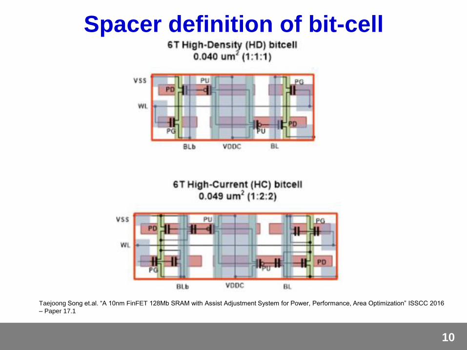
Spacer definition of bit-cell
Taejoong Song et.al. “A 10nm FinFET 128Mb SRAM with Assist Adjustment System for Power, Performance, Area Optimization” ISSCC 2016
– Paper 17.1
10

Bit-Cell Evolution – 22nm
Fully Gridded
• 3D device based
Tight Cuts
• Double poly cut
Eric Karl “A 4.6GHz 162Mb SRAM Design in 22nm Tri-Gate CMOS Technology with Integrated Active VMIN-Enhancing
Assist Circuitry,” ISSCC 2012
1-1-1 Cell (Pu-Pa-Pd) 1-1-2 Cell (Pu-Pa-Pd)
11

eDRAM
Next highest speed class of Memory
Bridges the gap between DRAM and SRAM
• Tcycle of 40nS for DRAM and 1ns for SRAM
• Density midway between SRAM and DRAM
Logic process based
• However needs process optimized for leakage
Best energy/bit (pJ/b) for large arrays
• Measured at equal capacity
12

eDRAM - Cell
Single Transistor – Single Capacitor
13
F. Hamzaoglu et.al. “A 1Gb 2GHz Embedded DRAM in 22nm Tri-Gate CMOS Technology”, ISSCC 2014, Paper 13.1

eDRAM - Cell
Open bit-line structure shown
• At the cross of WL and BL there is a cell
• Needs 2 poly tracks in this cell
14

eDRAM - Cell
Bit-line pickups along with capacitor pickup
• Note: Metal pitch need 1½ metal tracks per cell
15

eDRAM - Cell
Capacitor is vertically integrated
• Multiple levels of metal
• Capacitor over BL (COB)
16

eDRAM - Cell
Capacitors are vertically integrated
• Plate connection is common to multiple capacitors
17
14fF
Plate Connection

Functionality
18

Cell Functionality
SRAM Cells
• State Retention
• Read Stability
• Write Stability
DRAM Cells
• Retention Time
Key Difference:
• SRAM ratios transistor strengths for read and write.
SRAMs are non-destructive in read-out
19

SRAM Cell Retention Stability
Eye opening – metric of stability
• Defined by transistor parameter variations, strength
• Retention Vccmin
20
Vb
Va
ab
WL
BL
BL
_B

SRAM Cell Read Stability
Idsat of access device competes with Idlin of pull-down device • NMOS to NMOS ratio determines stability
Vb
Va
a
b
WL
BL
BL
_B
Vcc Vcc
0 1
21

SRAM Cell Write Stability
Access device Idsat to PMOS Idsat ratio
• NMOS to PMOS ratio
22
Vb
Va
a
b
WL
BL
BL
_B
Vcc 0
0 1

DRAM Cell Functionality
Failure of cell is in loss of state with time
DRO (destructive read out) non-ratioed write and read
Special access transistor with very high Vt
e.g. 15fF capacitor with 0.1msec retention requires pA of leakage per device
Leakage mechanism – subthreshold, junction, adjacent cells, capacitor, gate and defects
WL WL WL
Hold
Vcc/2
Vcc/2
0
1
Write disturb 0 Write disturb 1
Vcc
0
1 0
0 0 0
23

Functionality - Assisted 6T operation
Shigeki Ohbayashi, et al "A 65-nm SoC Embedded 6T-SRAM Designed for Manufacturability
With Read and Write Operation Stabilizing Circuits,” JSSCC April 2007
24
Read Assist
Write Assist
Collapse Array Vdd
Negative BL
Raise WL in steps Under-drive WL
Suppress BL Raise Vss

Adaptive WL Read-Assist
Dynamic WL under-drive
• Skew corner tracking
• Applied to die which are
read-stability limited
Intel – P. Kollar, et al “A 32 nm High-k Metal Gate SRAM With Adaptive Dynamic Stability
Enhancement for Low-Voltage Operation,” IEEE JSCC, Jan 2011
25

Modulating Bit-Line Voltage
IBM: H. Pilo, et al “64Mb SRAM in 32nm High-k Metal-Gate SOI
Technology with 0.7V Operation Enabled by Stability,
Write-Ability and Read-Ability Enhancements” ISSCC 2011
Read-Assist
Precharge of BL to lower than Vdd
Write-Assist
Capacitive negative BL drive
26

Vdd SRAM Based Assist
IBM: PILO et al. “Sram Design in
65nm Featuring Read-Write Assist
Circuits,” JSSC 2007
Per BL Sense Dynamic BL read assist
27

Performance

Frequency relationship
Modern designs span the V-F range
• Circuit optimality – only possible at a single V
Memory arrays designed not to be the Freq limiter
0.25
0.5
1
2
0.2 0.4 0.6 0.8 1 1.2 1.4
Re
lati
ve
Fre
qu
en
cy
Voltage
Gate DelayEquation
Wire Loaded
Ideal
𝑮𝒂𝒕𝒆 𝑫𝒆𝒍𝒂𝒚 = 𝑽𝒅𝒅/𝟐
𝑽𝒅𝒅 − 𝑽𝒕 𝟐
4X
Fre
qu
en
cy
29

Small Signal SRAM I/O Slice
3
3.5
4
4.5
5
5.5
6
6.5
7
7.5
8
1 100 10000 1000000 1E+08
N Memory Size (bits)
sig
ma t
arg
et
Cell target
Ysel Target
SA Target
DPM=10
R=256
M=32
Half of a SRAM I/O Slice
SAO
SAO _ B
S A
E
Do
S A
P C
H
R Y
S E
L [ 7
: 0 ]
W L [ 1
]
W L [ 0
]
W L
[ 2 5
4 ]
W L
[ 2 5
5 ]
P C
H
SAO _ R
W Y S
E L [ 7
:
0 ]
30

SRAM Cycle – 2 Clk Array
CLK
WL
SAPCH SAE
PCHRYSEL
BL/
BL_B
SAODOTsao
Tsa
Tcycle
1 2 Functional Race WL SAE Power Race WL PCH
Performance specification: clock cycles, frequency
31

BitLine Development
Speed dependant on Iread and bit-line cap
Power is not the classical CV2F
• Linear dependence on V, may be independent of F
Voltage
𝑽𝒃𝒍 =𝑰𝒓𝒆𝒂𝒅 × 𝑻
𝑪𝒃𝒍
T
Vbl
𝑷𝒐𝒘𝒆𝒓 = 𝑰𝒓𝒆𝒂𝒅 × 𝑽𝒅𝒅𝑻
𝑻𝒄𝒚𝒄𝒍𝒆
𝑷𝒐𝒘𝒆𝒓 = 𝑪𝒃𝒍 × 𝑽𝒃𝒍 × 𝑽𝒅𝒅 × 𝑭
𝑷𝒐𝒘𝒆𝒓 = 𝑪𝒃𝒍 𝑰𝒓𝒆𝒂𝒅 × 𝑻
𝑪𝒃𝒍𝑽𝒅𝒅 × 𝑭
32
Example:
Assumption - Iread = 10uA
Cbl = 20fF
T = 1/2GHz = 500pS
Vbl = 0.25Volts

Sense-Amplifier Basics
SA
O
SA
O_
B
SAE
Do
SAPCH
YSEL
yselT
puT
pdT
Tsa
Tsa
o BL_B
SAE
Sao
Tsa
Tsao
BL
SAPCH
Pairwise change device by sigma target
Cycle Time Target
33

Array Performance
Performance is in GHz range
• Shorter bit-lines to achieve logic performance
compatibility
2 Cycle Arrays
34

Small Signal DRAM I/O Slice
Folded bit-line architecture
only one of the bit-lines in the pair is activated
Sense-amplifier per bit-line pair
sense-amplifier does a read followed by write-back
Post sense-amp YSEL mux
Write is done by loading the sense-amplifier
Example 256rows X 2sectors X 32 = 2KBytes
S A
N
Di
Y S
E L
[ 3 1
: 0 ]
W r i t
e
Do
BL
W L [ 0
]
BL _ B
W L [ 1
]
W L [ 2
]
W L [ 3
]
W L [ 2
5 5
]
W L [ 2
5 4 ]
W L [ 2
5 3
]
W L [ 2
5 2 ]
V c c / 2
P C
H
S A
P
35

DRAM Cycle
Interleaving is used to approach thoughput of SRAM
CLK
Tcycle
PCH
WL
Cell node
BL/BL_B
SAN SAP
YSEL readwrite
Do
Lower Frequency
Longer cycle time
accommodate write-back
0 1 2 3
3cycle, 4 or higher
36

DRAM Sense operation
Signal does not increase with time
Offset causes functional failure
• Cell and bit-line determines Tsa
SAN
YSEL
PCH
SAP
puT
pdT
WL
SAN
Tsa
Tsao
BL
BL_B
Tsa
Tsa
o
SAP
37

eDRAM – Cycle Time
Paper 13.1 – 6 cycles to complete
38

eDRAM – Array Performance
Slower than SRAM ( ~6X) but clocks in the GHz
• 3X more clock cycles, 2X freq. at same voltage
39

From I/O Slice to SubArray
Xdecoder - Word-Line driver predecode one-hot addresses are used to activate a single word-line
Power saving through sleep devices activating a group of word-line drivers
WL & SAE split at POD
(point of divergence)
(32+1) I/O Slices
SRAM 256 cells per WL
DRAM 1024 cells per WL
16KB SRAM
64KB DRAM
32 dout + 1 redundancy
J x K
I x J x K
SAGate WLGate
PreAddrL [ I ]
PreAddrM [ I ]
PreAddrH [ I ]
POD Timing
S A
E
40

Sub-Array to Unit
Data Chunking
bus runs at full frequency
Redundancy shift-mux structure for column group replacement
row replacement, block replacement for other dimension
ECC multi-cycle operation
SECDED, DECTED, transparent ECC
32 SubArrays
512KB SRAM
2MB DRAM
D0
D1
D28
D2
9D
30
D3
1D
32
D0
D1
D28
D2
9D
30
D3
1
0
0
0
0
1
1
Multi-Level BUS routes
Red
un
dan
cy
Mu
x
EC
C
Glo
bal
Lo
gic
2
Glo
ba
l L
og
ic 1
0 1 2 3 4 5 6 7 8 9 10 11 12 13
chunk chunk WL SA chunk chunk
Ecc Gen 0 1 0 1 Ecc Fix
Bus Transit decode Bus Transit
41

Area

Area – Cell Size
14nm Technology
• Cpp = 70nm, FinPitch = 42
• HDC = 140nm x 357nm, LVC = 140nm x 320nm
Contacted Poly Pitch: Cpp = 70nm
Fin Pitch: FP = 42nm
HDC = 2 Cpp x 8.5 FP
X –
Bit
-Lin
e d
irecti
on
Y – Word-Line direction
LVC = 2 Cpp x 10 FP
Eric Karl “A 0.6V, 1.5GHz 84Mb SRAM Design in 14nm FinFET CMOS Technology,” ISSCC 2015, Paper 17.1
43

Area – Cell Size
2 Cpp x 2x(4/3) FP
22nm Process
Cpp = 90nm
Fp = 60nm
8.5 / 2.667
3.2X denser
F. Hamzaoglu et.al. “A 1Gb 2GHz Embedded DRAM in 22nm Tri-Gate CMOS Technology”, ISSCC 2014, Paper 13.1
44
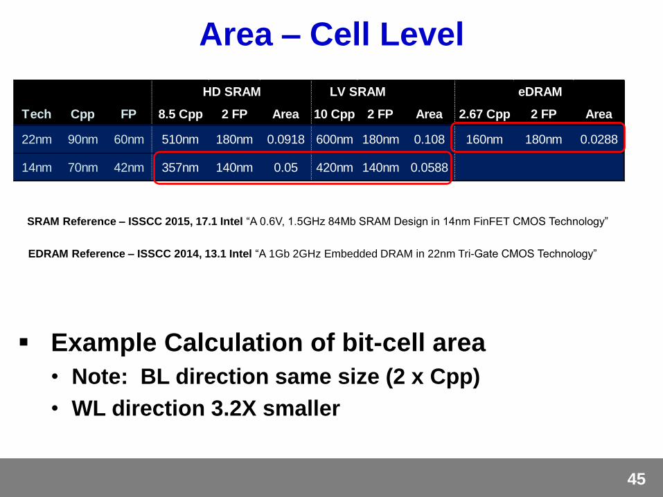
Area – Cell Level
Example Calculation of bit-cell area
• Note: BL direction same size (2 x Cpp)
• WL direction 3.2X smaller
Tech Cpp FP 8.5 Cpp 2 FP Area 10 Cpp 2 FP Area 2.67 Cpp 2 FP Area
22nm 90nm 60nm 510nm 180nm 0.0918 600nm 180nm 0.108 160nm 180nm 0.0288
14nm 70nm 42nm 357nm 140nm 0.05 420nm 140nm 0.0588
HD SRAM LV SRAM eDRAM
EDRAM Reference – ISSCC 2014, 13.1 Intel “A 1Gb 2GHz Embedded DRAM in 22nm Tri-Gate CMOS Technology”
SRAM Reference – ISSCC 2015, 17.1 Intel “A 0.6V, 1.5GHz 84Mb SRAM Design in 14nm FinFET CMOS Technology”
45

Area - LVC SubArray
SubArray efficiency (73%) – Logic is 36% of bit-cell area
bitcells
10 FP x 4 = 1.68um
FP = 42nm
Cpp = 70nm
258 x
2 x
2 C
pp =
72.2
4u
m
+24%
ovhd =
89.6
0u
m
Assume:
+25% in IO Col
+10% in WL
(snap to 2FP, 2Cpp)
89.6
0u
m
Bitcells = 114.24um
+ Row Decoder (+10%) = 125.664um
~16KB
46

Area – eDRAM SubArray
Substantially similar (2X bits with 1 node gap)
• 13.1 mentions 65% sub-array efficiency.
(128+
2)x
2 x
2 C
pp =
46.8
um
+4
0%
ovhd =
65.5
2u
m
Substantially more IO column overhead – per bit sense and write
Example calculation
Bitcells = 165.12um
+ Row Decoder (+10%) = 181.68um
~32KB
47
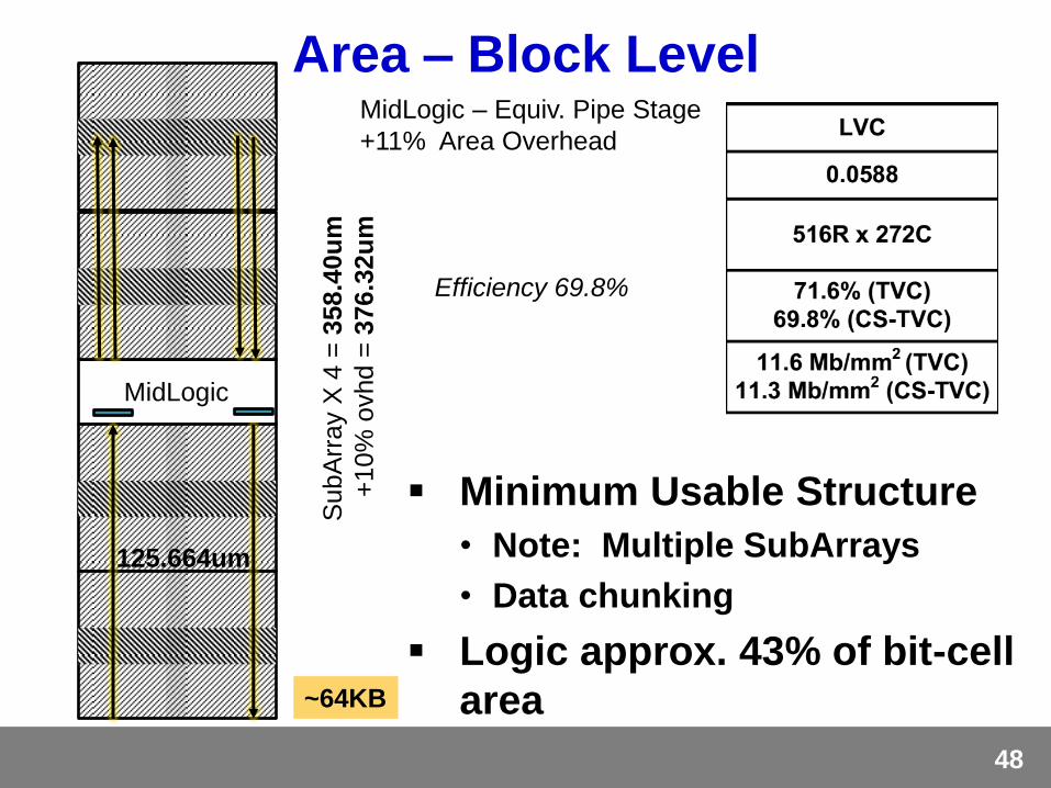
Area – Block Level
Minimum Usable Structure
• Note: Multiple SubArrays
• Data chunking
Logic approx. 43% of bit-cell
area
MidLogic
MidLogic – Equiv. Pipe Stage
+11% Area Overhead
SubA
rray X
4 =
358.4
0u
m
+10%
ovhd =
376.3
2u
m
125.664um
Efficiency 69.8%
~64KB
48

Area - Top
ECC in modern arrays forces line accesses
• Area Efficient Arrays are relatively large
‒ Example 65% logical array efficiency, ~70% physical efficiency
Explains 40%-50% efficiency of caches.
Need 8 Blocks for a cacheline
Data Bits 64 x 8b 512
DECTED 2 x 10b +1 21
Spare/Red ~1 per SubA 11
Total 544
CacheLine
Logical to Physical
Adders:
ECC +4%
Col Red. +2%
Row Red. +.7%
0.5MB
1005.312um
376.3
2u
m
49

Power
50

Cost of Walking Bits
Energy related to cost of switching wires
• Cap per unit mm – roughly invariant (geometry related)
Relative Permittivity ~3.0
Wikipedia is your friend – Lo K Dielectric
W = S = H
Cap per unit mm
Combination of parallel plate
Capacitor and Coaxial Cap
2 x Pi x Eo x Er / ln(2.2)
Cwire ~ 200fF/mm
Modulated by width and spacing
(within limits)
51

Calculating Power
Power = Cdyn x Vswitch x Vsupply x Freq
• For logic circuits Vswitch = Vsupply = Vdd
• Cdyn x Vdd2 x F
𝐂𝐝𝐲𝐧 =𝑷𝒐𝒘𝒆𝒓
𝑽𝒅𝒅𝟐 ×𝑭𝒓𝒆𝒒
Leakage Power
• Physical bit-cell count
• Leakage per bit-cell
• Uplift to account for distribution of bit-cell leakage
‒ Assumes that Logic can be extensively power-gated
52

Cost of Walking Bits
Repeater Segment length depends on wire resistance
Cdyn per unit length is roughly invariant
Wire length: L
No. of segments : N
Cseg Cseg/4
Cseg = Cwire / N
Switched Cap per mm = N x Cwire/N x ( 1 + ¼ )
Roughly Cwire x 1.25
𝐶𝑑𝑦𝑛 = 0.5 × 0.5 × 𝐶𝑤𝑖𝑟𝑒 × 1.25
Average Actvity Factor
(0.38 if encoded)
Clock Wires
𝐶𝑑𝑦𝑛 = 𝐶𝑤𝑖𝑟𝑒 × 1.25 Buses
NRZ effect Clock
DataCdyn = 0.0625pF/mm
53

Wire Cdyn
Repeater placement and sizing are generally
near optimal
75%
80%
85%
90%
95%
100%
80% 100% 120% 140% 160%
Rela
tive W
ire S
ped
vs M
ax
Relative Cdyn/mm
Repeater segment too short R
epeate
r segm
ent
too
lon
g
54

Global Walks
Data Movement Power
accounted in terms of BW
1005um 376u
m
376u
m
376u
m
376u
m
Avg. ~880um
2MB
Recap: 2GHz – 14nm design
0.5MB arrays, 32B din + 32B dout,
2GHz, 2 clock Tcycle
Freq 2GHz
Vdd 0.8V
BW 128GB/s
Global
Avg. Walk 878.5um
Act. Fact.
NRZ
Wire/Leaf Scale 1.04
Cdyn 57.2fF
Edyn 0.8V 36.6fJ
Power 128GB/s 37mW
Data
0.5
0.5
533b/512b
GB/s X 8 X Cdyn x V2
55

Clock, Address, Control
At the global level data movement
dominates
1005um 376u
m
376u
m
376u
m
376u
m
Ctrl, Clk ~2574um
2MB
13 address bits per group
3 control bits, 1 clock
gated in this example
Global Global Global Global
Avg. Walk 878.5um 1381um 2574um 2574um
Act. Fact.
NRZ
Wire/Leaf Scale 1.04 0.03 0.006 1.5
Cdyn 57.2fF 0.96fF 0.9fF 1.0pF
Edyn 0.8V 36.6fJ 0.61fJ 0.6fJ
Power 128GB/s 37mW 1mW 1mW
Clk Power 2GHz 1.2mW
0.5 0.5
0.21875 0.5 1
1
Data Address
0.5
0.5
Control Clock
Addr ~1381um
Clk May not be BW depedent
Address 1-hot
13b/512b
3b/512b
56

Address Encoding
Sparse Encoding – powerful technique to
reduce control and address power
Can be applied to data-buses – DBI drops AF to
38%
3 to 8
1 h
ot
A[2
:0]
101
00001000
3 to 8
1 h
ot
111
00000001
3 to 8
1 h
ot
111
00000001
A[5
:3]
A[8
:6]
0
1
2
3
127
126
125
124
123
Activity factor ~21% -- (7/8 x 2/8)
57

Block Block Block Block
Avg. Walk 98.56um 143.4um 143.4um 1479um
Act. Fact.
NRZ
Wire/Leaf Scale 1.06 0.19 0.047 16
Cdyn 6.5fF 0.74fF 0.42fF 5.9pF
Edyn 0.8V 4.2fJ 0.47fJ 0.27fJ
Power 128GB/s 4mW 0.5mW 0.3mW
Clk Power 2GHz 7.6mW
0.5 0.5
0.21875 0.5 1
1
Data Address
0.5
0.5
Control Clock
Block Walk
Data movement dominates at local level
• Clock power tapers as we go to global level
Active
1 subarray + ½ mid 1.5 subarray + ½
mid
12x8/512
68x8/512
3x8/512
clk
18um x 68 + 126 +
1.5 Subarray
126um
18u
m
58
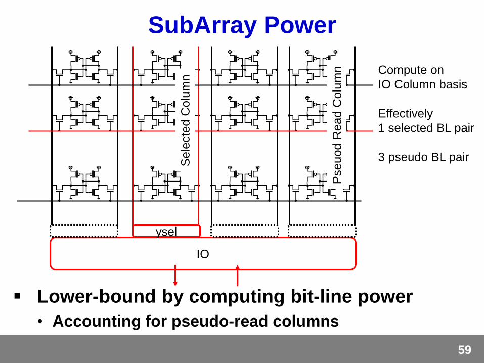
SubArray Power
Lower-bound by computing bit-line power
• Accounting for pseudo-read columns
IO
ysel
Sele
cte
d C
olu
mn
Pseuod R
ead C
olu
mn
Compute on
IO Column basis
Effectively
1 selected BL pair
3 pseudo BL pair
59
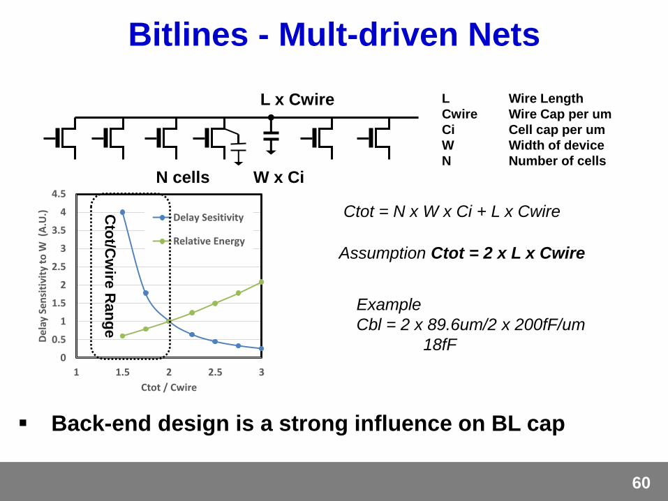
Bitlines - Mult-driven Nets
Back-end design is a strong influence on BL cap
W x Ci
L x Cwire L Wire Length
Cwire Wire Cap per um
Ci Cell cap per um
W Width of device
N Number of cells
0
0.5
1
1.5
2
2.5
3
3.5
4
4.5
1 1.5 2 2.5 3
Del
ay S
ensi
tivi
ty t
o W
(A
.U.)
Ctot / Cwire
Delay Sesitivity
Relative Energy
N cells
Ctot = N x W x Ci + L x Cwire
Assumption Ctot = 2 x L x Cwire
Cto
t/Cw
ire R
an
ge
Example
Cbl = 2 x 89.6um/2 x 200fF/um
18fF
60

SubArray Power
Embedded memories – sub-array power is non-
negligible
Selected Pseudo Selected Pseudo
BL Cap 17.9fF 14.3fF 17.9fF 14.3fF
Avg BL Swing 0.2V 0.25V 0.8V 0.25V
Vsw/Vdd 25% 31% 100% 31%
Wire Scale 1.0625 3.1875 1.0625 3.1875
Effective Cap 4.8fF 14.3fF 19.0fF 14.3fF
Cdyn
Power 128GB/s
19.0fF 33.3fF
34mW19mW
WriteRead
BL Length selected
½ Subarray 45um
Pseudo read length accounts
only for bit-cell dimension 36um
Scale swing based
on cap
1 pair for every di/do
3 pseudo pairs
* Accounts only for bit-line power – actual power higher (upper bound ~2X)
Unaccounted: Word-line, Control, Timer, Write Assist, Read Assist
61

37.5mW, 40%
0.6mW, 1%
0.6mW, 1%
4.3mW, 5%0.5mW, 0%0.3mW, 0%
8.8mW, 9%
26.8mW, 29%
14.4mW, 15%
Global - Data
Global - Address
Global - Control
Local - Data
Local - Address
Local - Control
Clock
Subarray - Rd=Wr
Leakage (1nA)
Power
Energy Efficient Storage ( example 0.1pJ/b)
Leakage at 1nA/b
Clock is
underestimated
SubArray
50% Rd – 50% Wr
62

Literature Survey
63

SRAM array – 22nm example
Lower voltage operation
• Heavily relies on circuits to avoid contention during
write and read processes
Eric Karl, “A 4.6GHz 162Mb SRAM Design in 22nm Tri-Gate CMOS Technology with Integrated Active VMIN-Enhancing Assist Circuitry”
64

SRAM array – 22nm
Classical – 6T assembled into 4 quadrant sub-array
65

22nm SRAM – Write Assist
Satish Dhamaraju, “A 22nm IA CPU GPU on die”
Eric Karl “A 4.6GHz 162Mb SRAM Design in 22nm Tri-Gate CMOS Technology with Integrated Active VMIN-Enhancing
Assist Circuitry,” ISSCC 2012
66

22nm SRAM – Read Assist
Vmin focus – multiple supply rails
• Importance of supply collaterals
67

ISSCC 2016 17.1 10nm FinFet SRAM..
A 10nm FinFET 128Mb SRAM with Assist
Adjustment System for Power, Performance,
Area Optimization
10nm node – 0.040um2 (HD) 0.049um2 (HC)
68

ISSCC 2016 17.1 10nm FinFet SRAM..
A 10nm FinFET 128Mb SRAM with Assist
Adjustment System for Power, Performance,
Area Optimization
10nm node – 0.040um2 (HD) 0.049um2 (HC)
WordLine Under Drive
Suppressed Bit-Line
Negative Bit-Line WordLine Over-Drive
WordLine Collapse
Dual Transient Word-Line
69
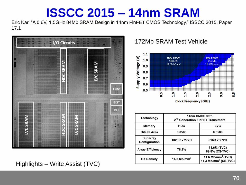
ISSCC 2015 – 14nm SRAM Eric Karl “A 0.6V, 1.5GHz 84Mb SRAM Design in 14nm FinFET CMOS Technology,” ISSCC 2015, Paper
17.1
172Mb SRAM Test Vehicle
Highlights – Write Assist (TVC)
70

ISSCC 2014 – 22nm eDRAM
F. Hamzaoglu et.al. “A 1Gb 2GHz Embedded DRAM in 22nm Tri-Gate CMOS Technology”, ISSCC 2014, Paper 13.1
Notables: Supply collaterals – positive pumps, negative pumps, mid-voltage generators,
Two level sense – local sense followed by global sense, high-voltage word-line drivers.
71

ISSCC 2014 – 22nm eDRAM
evaluate restore precharge
2Mb ½ bank
72

Micro 2016
Questions