direct copper bonding for power interconnects: design
TRANSCRIPT
HAL Id: hal-01207014https://hal.archives-ouvertes.fr/hal-01207014
Submitted on 30 Sep 2015
HAL is a multi-disciplinary open accessarchive for the deposit and dissemination of sci-entific research documents, whether they are pub-lished or not. The documents may come fromteaching and research institutions in France orabroad, or from public or private research centers.
L’archive ouverte pluridisciplinaire HAL, estdestinée au dépôt et à la diffusion de documentsscientifiques de niveau recherche, publiés ou non,émanant des établissements d’enseignement et derecherche français ou étrangers, des laboratoirespublics ou privés.
Direct Copper Bonding for Power Interconnects:Design, Manufacturing, and Test
Bassem Mouawad, Benoit Thollin, Cyril Buttay, Laurent Dupont, VincentBley, D. Fabregue, Maher Soueidan, Benoît Schlegel, Julien Pezard, Jean
Christophe Crebier
To cite this version:Bassem Mouawad, Benoit Thollin, Cyril Buttay, Laurent Dupont, Vincent Bley, et al.. Di-rect Copper Bonding for Power Interconnects: Design, Manufacturing, and Test. IEEE Trans-actions on Components, Packaging and Manufacturing Technology. Part A, ManufacturingTechnology, Institute of Electrical and Electronics Engineers (IEEE), 2015, 5 (1), pp.143-150.10.1109/TCPMT.2014.2376882. hal-01207014

SUBMISSION ON IEEE TRANS ON COMPONENTS, PACKAGING AND MANUFACTURING TECHNOLOGY 1
Direct Copper Bonding for Power Interconnects:Design, Manufacturing and Test
Bassem Mouawad, Benoit Thollin, Cyril Buttay, Member, IEEE, Laurent Dupont, Vincent Bley,Damien Fabregue, Maher Soueidan, Benoıt Schlegel, Julien Pezard, Jean-Christophe Crebier
Abstract—3D power module structures allow for better coolingand lower parasitic inductances compared to the classical planartechnology. In this paper, we present a 3D technology that uses aninnovative assembly method (direct copper-to-copper bonding).The concept and manufacturing process of this technology isdescribed in details. Accurate electrical characterization is thenperformed to compare its performance with that of classicalplanar structures.
Index Terms—Three-dimensional packaging, power electron-ics, Spark Plasma Sintering, semiconductor device packaging
I. INTRODUCTION
THE VAST MAJORITY of the power modules producedtoday have the structure presented in figure 1(a) (planar
structure, [1]): the bottom side of the power semiconductordevices is attached to a ceramic substrate (direct bonded cop-per, DBC), usually using solder, and the top side is connectedusing wirebonds.
Although widely used, this planar structure has some draw-backs. The wirebonds have reliability issues when submittedto thermal cycling [2], and they generate stray inductances inthe order of 10 nH [3], causing switching losses and electro-magnetic interferences (EMI). Other limitations of the planarstructure include its large surface area (because all electricalinterconnects are performed on the same plane, the uppermostcopper layer of the DBC substrate), and its limited thermalperformance. Indeed, with this structure, the heat dissipatedby the power dies is removed through the bottom side only.
As a consequence, many alternative structures have beenpresented in the recent years. These 3-dimensional (3D)structures offer replacement for the wirebond interconnects. Areview of some of the 3D structures is proposed in [4] and [5],but although they present innovative interconnect solutions,most of them still provide cooling through one side of the dieonly.
3D structures with double-side cooling capability are listedin [6]. Most have a “sandwich” configuration, i.e the dies aresandwiched between two DBC substrates. They differ in theway the dies are bonded to the substrates and in the way theyare cooled. Regarding bonding solutions, one can list solderbumps [7], soldered copper cylinders [8], diffusion-bondedcopper posts [9], direct soldering [10], or more recentlypressure contacts [3].
Among these, we will focus on the “copper posts” structure(Fig. 1(b)). Here, copper posts are electrolytically grown onthe surface of the power dies. They are then bonded to themetal layer of a DBC substrate [9]. In this previous study, alayer of tin was used to join the copper elements.
Fig. 1. Power electronics packaging concepts: (a) the planar structure, whichis widely used today and (b) a ”3D” concept that allows cooling of the dieon both sides.
Recently, we presented a simpler solution to bond twocopper parts together: the direct copper-copper bonding pro-cess [11], in which the two parts are simply pressed againsteach other in vacuum and heated to 200 to 300 °C. This resultsin a strong bond, without requiring any additional bonding ma-terial. This technique and its application to power electronicspackaging as a replacement for soldering are presented below.
In this paper, we describe the manufacturing process ofa copper-post-based sandwich structure which is assembledusing direct bonding only (section III). An electrical test set-up, dedicated to the accurate characterization of the assembly,is presented in section IV. The corresponding results are givenin section V, and discussed in section VI.
II. CONCEPT OF THE STRUCTURE
The power module concept developed in the present ar-ticle is shown in Fig. 1(b). A power semiconductor die isinserted between two DBC substrates, allowing cooling fromboth sides. On the top side of the die, some copper postsprovide spacing between the die and the top substrate. Thisspacing prevents the top substrate from short-circuiting theedge protections of the die.
The posts are also useful to accommodate height differencesbetween dies in a multi-chip power module: different types ofdies are commonly used in a single module (such as IGBTand diode, for example), and they do not always have thesame thickness. This is not an issue for a “classical” powermodule (Fig. 1(a)), as it uses wirebonding. In the case of the“sandwich” package (Fig. 1(b)), however, the topside contactsof all the dies must be aligned for proper connection with thetop substrate. The copper posts can then compensate for thethickness differences between the dies.
Depending on the form factor of the copper post, they mightalso offer some mechanical flexibility. This is attractive tomanage the differences in coefficient of thermal expansion

SUBMISSION ON IEEE TRANS ON COMPONENTS, PACKAGING AND MANUFACTURING TECHNOLOGY 2
(CTE) between various elements of the package. For practicalreasons, however, the posts presented in this article have avery low form factor (they are much larger than high), so noflexibility is expected here. Copper posts with a much largerform factor (twice as high as they are large, or more) andwith finer pitch (80 µm) have already been presented by otherresearchers [12].
Another innovative feature of the structure is the solder-free approach: the die (with copper posts) and both DBC sub-strates are bonded together directly, without using any bondingmaterial. The evaluation of the direct bonding technique wasdescribed in [11]. It is shown that this technique (describedbelow) offers a very high bonding strength, about half thetensile strength of copper.
Copper posts could be used for both sides of the die or,as described in Fig. 1(b), for one side only. The structuredescribed in this paper has copper posts on one side of thedies only. The backside of the dies (silver) is directly bondedto the polished copper substrate. Both sides of the die arebonded in one step.
III. MANUFACTURING PROCESS
The main step to manufacture the power module fromFig. 1(b) is to electrolytically grow the copper posts on topof the dies. This must be performed at the wafer-level, beforethe wafer is singulated. In parallel, the copper layer of thesubstrate must be polished, to facilitate the bonding process.Finally, the three elements (two substrate and one die) arebonded together using a press, in vacuum.
These three steps will now be described in details.
A. Preparation of the dies
Fig. 2 presents the process work-flow required to growcopper posts on dies.
The starting point is a pre-processed wafer, with the powerdevices already manufactured. This wafer must be removedfrom the production line just before the dicing step, where itis cut into individual dies.
In our case, the wafer (6 in, 150 mm) was supplied byMicrosemi and consists in 6×6 mm2, 600 V, silicon diodeswith an aluminium layer on top, and a silver layer on theback. As we could not process such a large wafer as a whole,we cut it into squares of 25 diodes each (see Fig. 3). Inthe remaining of this article, the term “wafer” will thereforedescribe this 25-diode fragment. Please note that the processpresented here can be applied to wafers of any size, providingsuitable manufacturing equipment is available.
A “seed” layer (25 nm Ti for adhesion, 300 nm Cu) isdeposited on top of the wafer by sputtering (Fig. 2(b)) to coverthe aluminium layer and the edge terminations of the diodes.This continuous layer is used both to provide a metal surfacecompatible with the copper posts, and to carry the current fortheir electrolytic growth.
The wafer is then placed in a custom-designed carrier, andlaminated (110 °C) with a patterned copper foil and somethick photosensitive dry film (Dupont Riston PM275, 75 µm-thick [13]) (c). This carrier provides an electric connection to
Wafer
Wafer
WaferWafer carrier
Wafer
UV
Wafer
Wafer
Wafer
Wafer
Diode Diode
Wafer carrier
Wafer carrier
Wafer carrier
Diodes wafer with Al top metal
Sputtering of Ti/Cu seed layers
Mounting of the waferon carrier, sealing withphotosensitive film
Exposure to UV tocreate micropost pattern
Development of film
Copper electroplating
Extraction from carrierand polishing of Cu excess
Stripping of photosensitivefilm and etching of Ti/Cu seed layers
Dicing of wafer
(a)
(b)
(c)
(d)
(e)
(f)
(g)
(h)
(i)
Fig. 2. Process flow of the copper posts manufacturing
"Wafer" (actually cut from a 6 in wafer)
30m
m
30mm
wiring for electroplating
PM 275 Dry film
Hot glue
Copper foil
Wafer carrier
Fig. 3. The wafer fragment (designed here as ”Wafer”) at the beginning ofthe process, and at step (e) in fig. 2.
the wafer for the electroplating step, as well as sealing fromthe electroplating bath. In step (d) and (e), the photosensitivelayer is exposed and developed (using a 1 wt% solutionof Na2CO3) to form molds for the growth of the posts. Aphotograph at step (e) is visible in figure 3. Note that the sizeof the posts (900×900 µm2) was chosen for practical reasons.With a proper development system (spraying system), muchsmaller posts are possible, as the nominal resolution of thephotosensitive film is 50 µm.
Some wires are then connected to the copper foil (f), and thewafer carrier is immersed in the electroplating bath (220 g/lCu2SO4, 32 ml/l H2SO4, 0.2 ml/l HCl, 2 ml/l Rubin T200-A,

SUBMISSION ON IEEE TRANS ON COMPONENTS, PACKAGING AND MANUFACTURING TECHNOLOGY 3
0 5 10 15 20 250
5
10
15
20
25
0
30
60
90
120
150
180
210
240
(a)
0 5 10 15 20 250
5
10
15
20
25
0
30
60
90
120
150
180
210
240
(b)
Fig. 4. Topology mapping of the wafer fragment after electroplating (a) andafter polishing (b). The color scale is in micrometers, x- and y-axis are inmillimeters.
8 ml/l Rubin T200-G and 2 ml/l Rubin T200-E). A copperelectrode is placed parallel to the wafer carrier, at 30 mmapproximately. The electroplating current (10 mA/cm2) issupplied by a Keithley 2602A source and measure unit (SMU).The deposition rate at this current level is approximately12 µm/h.
After 7 h, the wafer carrier is removed from the electro-plating set-up, and the wafer is extracted from the carrier. Thetop surface is then polished (Logitech PM5, LAAS, Toulouse)to remove the excess copper and to planarize the copperposts (Fig. 2(g)). A mapping, performed on a wafer beforeand after the polishing using a Dektak 150 profilometer, isvisible figure 4. The large differences in height caused by anin-homogeneous current distribution during the electroplating(Fig. 4a) are removed, resulting in a constant post height acrossthe wafer (Fig. 4b).
The photosensitive film is then dissolved in a 3%wt NaOHsolution. The seed layers are removed by dipping the wafer ina copper etch solution (Transene APS-100, 1 min), followedby a titanium etch solution (5 % BOE, 1 s) (Fig. 2(h)). Finally,the wafer is singulated using a Disco DAD 3220 dicing saw
(i).Note that all the steps of this process (sputtering, mask-
ing, electroplating, polishing etc.) are commonly used in theelectronic industry. It could therefore be integrated to thewafer manufacturing. In particular, this would make it directlypossible to produce dies with a suitable topside metal finish(copper), instead of depositing Ti/Cu on top of the standardaluminium metallization. The electroplating step takes a longtime (7 h), but this does not seem to be incompatible with in-dustrial production, as posts with a comparable height (80 µm)are commonly grown on microelectronic wafers [12].
B. Preparation of the substrates
Direct Bonded Substrates (DBC), from Curamik, are usedfor this study. To reduce the surface roughness of their copperlayers (initial Ra>2 µm) , they are polished, starting with220-grit SiC paper, down to 1 µm diamond paste and 50 nmsilica.
After polishing, the DBC substrates are cleaned in acetoneand ethanol, then de-oxidized using a 5 % HF solution, rinsedin de-ionized water and dried using a nitrogen blow nozzle.Once the substrates cleaned, the assembly process is performedimmediately (within one hour) to avoid re-oxidation of thecopper.
C. Assembly process
The direct bonding process, used here to assemble thesandwich package, is investigated in details in [11]. Basically,it consists in pressing the elements to be bonded together,and to heat them up to a given temperature (here from200 and 300 °C), using a special pressing tool (a so-calledSpark Plasma Sintering –SPS– press). It is comparable to athermo-compression, but the bonding strength was found to bemuch higher than previously reported, with tensile strengthsmeasured at up to 261 MPa (to be compared with 365 MPafor a bulk copper sample).
For the results presented here, due to equipment availability,two bonding tools are used: the same SPS press as usedin [11] (FCT Systems HP D25/1), and a Rapid ThermalAnnealing (RTA) furnace, equipped with a pressing fixture(Jipelec Jetfirst 100). Both systems allow bonding in vacuum,with very fast heat-up ramps. The main difference are theheating system (Joule heating for the SPS, halogen lamps forthe RTA), and the pressing force (5 kN for the SPS, 0.26 kNfor the RTA). In the SPS, a custom graphite jig [14] is used toreduce the actual force applied to the assemblies, and to avoiddamaging the dies with an excessive force. As a consequenceof using this jig, the actual force applied to the assembliesprocessed with the SPS could not be measured.
The bonding is performed using the following parameters:heat-up ramp 100 °C/min, bonding time 5 min, bondingtemperature 200 or 300 °C. The whole bonding process takesplace in vacuum.
1) Preliminary electrical test: prior and after assembly, thediodes are electrically controlled to detect any damage thatcould be caused by the packaging process. In both cases, weuse a Keithley 2410 SMU connected to a probe station (with
SUBMISSION ON IEEE TRANS ON COMPONENTS, PACKAGING AND MANUFACTURING TECHNOLOGY 4
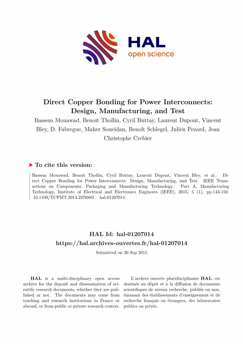
TABLE ISHEAR TEST MEASUREMENTS PERFORMED ON SANDWICH STRUCTURES
BONDED USING SPS AND RTA. F IS THE SHEAR FORCE, S THE TOTALCONTACT SURFACE OF THE CU POSTS/SUBSTRATE INTERFACE, AND τ IS
THE CORRESPONDING SHEAR STRENGTH.
SPS RTAT F S τ T F S τ
(°C) (N) (mm2) (MPa) (°C) (N) (mm2) (MPa)300 113 2.6 43 300 199 11.8 16300 184 8.9 20 300 93 7.3 12300 275 8.4 32 200 133 5.2 25300 275 8.9 30 200 187 4.0 46200 181 7.0 25200 21 1.1 18200 31.5 5.6 5.6200 176.5 8.4 21
Fig. 5. Fracture surface after a shear test: most copper posts were separatedfrom the die (left) and stayed on the substrate (right). In some cases (bottomright post on the die), the fracture occurred in the silicon, indicating a goodbond quality.
a 4-probe configuration). Forward and reverse characteristicare performed, but with limited forward current (1 A, limitedby the SMU and the probes) and reverse voltage (limited to-300 V to prevent arcing in air).
After packaging, all diodes show a small improvementof their forward characteristic (about 60 mV lower forwardvoltage at 1 A current as compared to the diodes with theelectroplated posts), and no change of the reverse current (inthe order of 30 nA at 300 V). The improvement of the forwardcharacteristic can be attributed to the test conditions: prior tothe assembly, the probes are connected to one copper postonly, hence injecting the current in a localized manner. Afterassembly, the probes are connected to the inner copper layerof the DBC substrate, which spreads the current among allcopper posts.
2) Mechanical testing of the assembly: In [11], the bondingtests were performed on bulk copper rods only. In order tomake sure that the direct bonding technique worked on morecomplex systems, 12 sandwich structures are assembled andmechanically tested (shear test). The results are visible intable I, with T being the assembly temperature, F the forcerequired to separate the top substrate from the die, S thesurface of the interface between the copper posts and thetop substrate, and τ = F/S the corresponding shear strength.The surface S was obtained by summing the surface of theposts that remained on the top substrate and the surface of theimprints left by the posts in the top substrate (when the failureoccurred at the post/substrate interface). Although the copper
DieDie
MicropostUpper DBC
Lower DBC
100µm300µm
Fig. 6. Cross-section of a DBC/diode/DBC assembly. The diode has micro-posts on top.
posts and the substrate are polished prior to assembly to ensuregood contact, the surface S is found to be significantly smallerthan expected for all samples: the expected value is 13 mm2
(16 posts with a 900×900 mm2 surface), while the measuredvalues range from 1.1 up to 11.8 mm2.
Several failure modes can be observed after shear test. Asan example, on Fig. 5, only 2 out of 16 posts remain on thedie. The other 14 separated from the die either at the seedlayer interface, or even within the silicon. The bottom leftpost on the substrate in Fig. 5 shows fragments of silicon. Onthe other samples (not shown here), the same failure modescan be observed, albeit in different proportions (more or lessposts remaining on the die, from small cracks in the siliconup to complete destruction of the die).
Given the small sample count, no significant effect can befound regarding the bonding equipment (SPS or RTA) and thebonding temperature (200 and 300 °C). The average shearstrength is 24.5 MPa (with 11.9 MPa standard deviation).In comparison, the MIL-STD 883 requires minimum shearstrength values always smaller than ≈ 6 MPa [15] (exact valuedepends on die size). This standard cannot be applied directlyhere, as it is intended for plain die attaches, not for posts,but it indicates that the values listed in table I are realisticfor the application. Note that some assemblies were attemptedusing a non-polished DBC substrate, but they all showed apoor adhesion (around 20 N), with all assemblies failing atthe post/substrate interface.
The cross-section of another assembly is visible in figure 6.The interface between the copper posts and the upper DBC isbarely visible.
IV. ELECTRICAL CHARACTERIZATION SET-UP
Thanks to its copper posts, the packaging solution presentedin this paper is expected to offer a very low resistance com-pared to aluminium wirebonds. The copper posts are indeedshorter, wider, and copper is a better electrical conductor thanaluminium.
As a consequence, we designed a specific characterizationset-up to perform accurate forward I(V) characterization up to200 A. It is described in this section, while the measurementresults are presented in section V.
SUBMISSION ON IEEE TRANS ON COMPONENTS, PACKAGING AND MANUFACTURING TECHNOLOGY 5
(a) Bottom side (b) Top side
30 mm
30 mm6 mm
6 mm
(c) Cross-section of the assembly
Die
Microposts
Substrates
Access to top Cu layer
protuding Cu pad (polished)
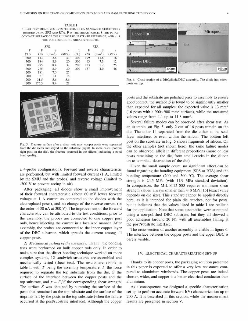
Fig. 7. Layout of the DBC substrates (a) and (b), and cross-section of theassembly (c).
A. Test vehicles
Two different packages are investigated, both containingthe same chip model: TO-247 plastic packages (Microsemi,reference APT60D60BG) and a sandwich package made usingthe process described in section III, with a design describedbelow.
1) TO-247 plastic package: For their characterization, thediodes are attached to a cold plate which is connected to achiller to control the ambient temperature. Kelvin (4-wire)connections are attached to the leads of the package, asclose as possible to the epoxy molding. This configurationminimizes the effect of the leads in the I(V) characterization,but does not cancel-out the resistance caused by the internalelements of the package, especially the wirebonds.
2) Sandwich package with Kelvin contacts: This package(see drawings in Fig. 7 and corresponding photograph inFig. 8) is designed to allow voltage measurement at variousplaces, to detect possible current balancing issues that mightbe caused by improper bonding of the posts. Some holes arelaser-drilled in the ceramic layer (see Fig. 7(c)) for currentinjection. Their location, directly above and below the die, ischosen to homogenize the current distribution.
A two-step copper etching technique is used to form apedestal on the inner surfaces of the substrate. This protrudingpart is used as an alignment feature to position the die duringthe assembly. It also simplifies the polishing step of thesubstrates (section III-B): only the surface directly involvedin the bonding need to be polished, not the entire surface ofthe substrate.
Finally, a graphite jig is used to align both substratesduring the assembly. The bonding is performed using the RTA
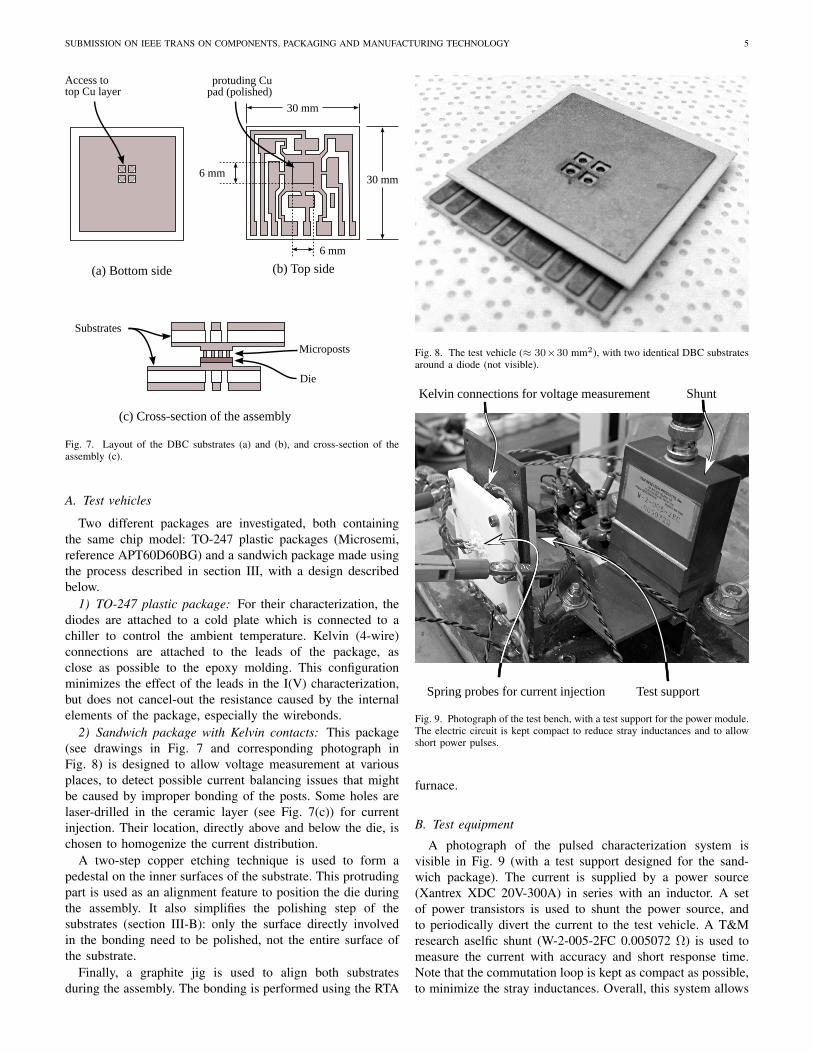
Fig. 8. The test vehicle (≈ 30×30 mm2), with two identical DBC substratesaround a diode (not visible).
Test supportSpring probes for current injection
ShuntKelvin connections for voltage measurement
Fig. 9. Photograph of the test bench, with a test support for the power module.The electric circuit is kept compact to reduce stray inductances and to allowshort power pulses.
furnace.
B. Test equipment
A photograph of the pulsed characterization system isvisible in Fig. 9 (with a test support designed for the sand-wich package). The current is supplied by a power source(Xantrex XDC 20V-300A) in series with an inductor. A setof power transistors is used to shunt the power source, andto periodically divert the current to the test vehicle. A T&Mresearch aselfic shunt (W-2-005-2FC 0.005072 Ω) is used tomeasure the current with accuracy and short response time.Note that the commutation loop is kept as compact as possible,to minimize the stray inductances. Overall, this system allows

SUBMISSION ON IEEE TRANS ON COMPONENTS, PACKAGING AND MANUFACTURING TECHNOLOGY 6
0.6 0.8 1.0 1.2 1.4 1.6 1.8 2.0Forward Voltage [V]
0
50
100
150
200Fo
rwar
dC
urre
nt[A
]
To 247Sandwich package
Fig. 10. Direct I/V characteristic for diodes packaged respectively in a T0-247 plastic package, and in the proposed “sandwich” package. Measurementsperformed at 20°C.
the measurement with pulses shorter than 10 µs and withcurrent levels up to 300 A.
V. EXPERIMENTAL RESULTS
The forward I(V) characterizations performed using the set-up described in section IV is visible in figure 10. Five diodesare used, two in a TO-247 package, and three in a sandwichpackage.
Contrarily to what was expected, the TO-247-packageddiodes offer a lower voltage drop than those in the sandwichpackages (200 mV lower for a 200 A forward current). Al-though all 5 diodes satisfy the specifications in the APT60D60datasheet (typical values: 1.6 V for 60 A, 1.9 V for 120 A),the relatively higher resistance of the sandwich package issurprising. For the bonding study presented in [11], the elec-trical resistance of the bonding interface was so small that wewere not able to measure it with our test setup (limited to aresolution of 100 µΩ.mm2).
VI. DISCUSSION
Part of the difference could be attributed to the diodes diesthemselves: the dies used in the sandwich and the T0-247package were probably not manufactured at the same time,and therefore could exhibit differences in characteristics.
Another explanation is related to the Ti/Cu metallizationthat is deposited to allow the growth of the copper posts(Fig. 2(b)). Surface (square) resistance measurement measuredwith a 4-probe set-up (aligned with a 1-mm pitch) are visiblein Fig. 11. The plain lines correspond to the 25 diodes ofan un-processed wafer fragment, and show little dispersion.The dotted lines correspond to the 25 diodes of a fragmentof the same wafer, after the Ti/Cu metallization. Not only isthe voltage-drop higher, but the dispersion is also much larger.Identical measurements (not presented in Fig. 11) show thatafter chemically removing the Ti/Cu metallization, the surfaceresistance returns to its original value (plain lines in Fig. 11),which proves that the aluminium layer is not affected.
0.00 0.05 0.10 0.15 0.20Voltage [mV]
0
20
40
60
80
100
Cur
rent
[mA
]
Initial condition (Al top)After sputtering of Ti/Cu seed layer
Fig. 11. square resistance measurement performed on the topside metalliza-tion of dies in the initial condition (aluminium) and after sputtering of theseed layer (Ti/Cu on top of the aluminium).
200 300 400 500 600 700 800Sputter time [s]
0
2
4
6
8
10
12
14In
tens
ity(x
1000
)
Cu2
Al2
02
TiAl2AlO2
TiOCuOCu2
Fig. 12. SIMS profiles performed on the same wafer as Fig. 11. Metals areplotted with a plain line (Titanium is barely visible, with a small bump overthe 500 s mark), and the oxides with dotted lines. It appears that there is ahighly oxidized interface between Al and Ti, and that most of the Ti layer isoxidized.
If the consequence of this higher surface resistance isobviously an increase in the series (vertical) resistance ofthe diode, it is difficult to actually calculate it: we do notknow which element of the Ti/Cu actually causes the increasein resistivity (is it at the interface between aluminium andtitanium? in the titanium or copper layer themselves?, atthe Ti/Cu interface?). Furthermore, the equations used tofind out the resistivity of a material from surface resistancemeasurement were developed for a conductive layer on aisolating (or semi-isolating) substrate. In our case, the layerthat needs characterization (Ti/Cu) is attached to a thickerconducting layer (aluminium).
From the process notes, it appears that a pressure change(increase from 3.10−6 mbar to 6.10−5 mbar) was observed inthe chamber during the Ti sputtering (this can be due to a leak

SUBMISSION ON IEEE TRANS ON COMPONENTS, PACKAGING AND MANUFACTURING TECHNOLOGY 7
or the degassing of the chamber). This might have caused theoxidation of the Ti layer, and resulted in a higher resistivity ofthis layer. This is confirmed by SIMS (Secondary Ions MassSpectroscopy, ) measurements performed (“Science et Surface,Ecully, France) on the same wafer as in Fig. 11 (see Fig. 12).It appears that the Ti/Al interface is strongly oxidized. Suchmeasurements were performed for two diodes of the wafer, thebest and the worst diodes from Fig. 11, but the SIMS profilesare identical.
As stated before, the Ti/Cu metallization is required inour process to enable copper electroplating on the standardaluminium finish of the diodes. In an industrial process, thiswould not be necessary as the diodes would be directlymanufactured with a suitable topside metal. Power deviceswith a thick copper metal layer have recently been intro-duced [16], and would probably be well-suited to copper postsinterconnects.
VII. CONCLUSION
A power module sandwich structure, based on copper-to-copper direct bonding has been presented in this article.Compared to existing solutions, no additional bonding material(solder or adhesive) is required.
The whole manufacturing process has been presented in de-tails and demonstrated on a diode wafer. Several modules havebeen assembled and show an acceptable bonding strength. Oneadvantage of this process is that most of the manufacturingsteps take place on the wafer, before singulation (“wafer-scalepackaging”), so many dies can be processed at the same time.
A dedicated characterization set-up has been developed,including specific DBC substrates and a test bench generatingshort current pulses.
Using this set-up, it was found that the resistance introducedby the sandwich packaging is slightly higher than that ofa conventional TO-247 package. An hypothesis is that thisdisappointing result can be attributed to the poor quality ofthe Ti/Cu seed layer used for the electroplating of the copperposts.
If the copper posts were to be implemented in an industrialprocess, it would be part of the diodes manufacturing process,and the Ti/Cu metallization would not be required. Therefore,we consider that the higher resistance of the sandwich packageas compared to the TO-247 is not an intrinsic problem of theproposed packaging solution.
ACKNOWLEDGMENT
The authors would like to thank M. Dupin, from Microsemi,and M. Trinel, from Richardson RFPD France, for supplyingthe diodes used in this study and the Agence Nationale deRecherche (ANR) for its support of this work through the grant“ECLIPSE”. Some of the manufacturing steps were performedon the 3DPHI platform.
REFERENCES
[1] W. W. Sheng and R. P. Colino, Power Electronic Modules: Design andManufacture, 1st ed. CRC, jun 2004.
[2] M. Ciappa, “Selected failure mechanisms of modern power modules,”Microelectronics Reliability, vol. 42, no. 4-5, pp. 653 – 667,2002. [Online]. Available: http://www.sciencedirect.com/science/article/B6V47-45CN6JG-8/2/9bab07a93f785fbcee637106dbe0ff07
[3] E. Vagnon, P.-O. Jeannin, Y. Avenas, J. Crebier, and K. Guepratte,“A Busbar Like Power Module Based On 3D Chip On Chip HybridIntegration,” in Applied Power Electronics Conference and Exposition,2009. APEC 2009. Twenty-Fourth Annual IEEE. IEEE, 2009, pp.2072–2078. [Online]. Available: http://hal.archives-ouvertes.fr/docs/00/39/68/84/PDF/Vagnon APEC.pdf
[4] L. Menager, C. Martin, B. Allard, and V. Bley, “Industrial and lab-scalepower module technologies : A review,” in Proceedings of the 32ndAnnual Conference of the IEEE Industrial Electronics Society (IECON),IEEE, Ed., Paris, France, nov 2006.
[5] J. Calata, J. G. Bai, X. Liu, S. Wen, and G.-Q. Lu, “Three-DimensionalPackaging for Power Semiconductor Devices and Modules,” AdvancedPackaging, IEEE Transactions on, vol. 28, no. 3, pp. 404–412, 2005.
[6] J. Schulz-Harder, “Review on Highly Integrated Solutions for PowerElectronic Devices,” in Proceedings of the Conference on IntegratedPower electronics Systems (CIPS), Nuremberg, mar 2008, p. 7p. [Online]. Available: http://www.electrovac.com/sprache2/n221666/n.html
[7] C. Gillot, C. Schaeffer, C. Massit, and L. Meysenc, “Double-SidedCooling for High Power IGBT Modules Using Flip Chip Technology,”IEEE Transaction on Components and Packaging Technology, vol. 24,no. 4, pp. 698–704, dec 2001.
[8] P. Solomalala, J. Saiz, A. Lafosse, M. Mermet-Guyennet, A. Castellazzi,X. Chauffieur, and J.-P. Fredin, “Multi-domain simulation platform forvirtual prototyping of integrated power systems.” in Power Electronicsand Applications, 2007 European Conference on, sept. 2007, pp. 1 –10.
[9] L. Menager, M. Soueidan, B. Allard, V. Bley, and B. Schlegel, “ALab-Scale Alternative Interconnection Solution of Semiconductor DiceCompatible with Power Modules 3D Integration,” IEEE Transactions onPower Electronics, vol. 25, no. 7, pp. 1667–1670, jul 2010.
[10] C. Buttay, J. Rashid, C. Johnson, F. Udrea, G. Amaratunga, P. Ireland,and R. Malhan, “Compact Inverter Designed for High-TemperatureOperation,” in Proc. IEEE Power Electronics Specialists ConferencePESC 2007, 2007, pp. 2241–2247.
[11] B. Mouawad, M. Soueidan, D. Fabregue, C. Buttay, B. Allard, V. Bley,H. Morel, and C. Martin, “Application of the Spark Plasma SinteringTechnique to Low-Temperature Copper Bonding,” IEEE Transactions onComponents, Packaging and Manufacturing Technology, vol. 2, no. 4,pp. 553–560, apr 2012, early Access.
[12] J. Kloeser and E.-A. Weissbach, “high performance flip-chip packageswith copper pillar bumping,” Global SMT and Packaging, article,may 2006. [Online]. Available: http://www.trafalgar2.com/documents/Technical Articles/6.5-kloeser.pdf
[13] DuPont, “PlateMaster PM200 Series: Data Sheet & Processing Infor-mation,” DuPont, Tech. Rep.
[14] B. Mouawad, C. Buttay, M. Soueidan, H. Morel, and B. Al-lard, “3-Dimensional, Solder-Free Interconnect Technology for High-Performance Power Modules,” in Proceedings of the Conference onIntegrated Power Systems (CIPS), Nuremberg, 2012.
[15] Test Method Standard Microcircuits, MIL-STD-883G Std., feb 2006.[16] K. Guth, D. Siepe, J. Gorlich, H. Torwesten, R. Roth, F. Hille, and
F. Umbach, “New assembly and interconnects beyond sintering meth-ods,” in Proceedings of PCIM, Nuremberg, may 2010, pp. 232–237.
Bassem Mouawad received the Ph.D. degree from”Institut National des Sciences Appliques” (INSA)in Lyon, France, in 2013. He was then a researchfellow in MATEIS Laboratory (INSA Lyon) wherehis research was mainly focused on the elaborationof materials by the means of flash sintering/bondingas well as on the mechanical properties of metallicalloys. In 2014, he joined the Power ElectronicsMachines and Control (PEMC) group at the Univer-sity of Nottingham, in Nottingham, United Kingdomwhere he is currently a research fellow. His current
research interests include packaging technologies for SiC devices.

SUBMISSION ON IEEE TRANS ON COMPONENTS, PACKAGING AND MANUFACTURING TECHNOLOGY 8
Benoit Thollin received the Ph.D. degree in Elec-trical Engineering from the University of Greno-ble, France, in 2013. After post-doctoral researchesin the Grenoble Electrical Engineering Laboratory(G2Elab), focusing on thermal management andthermal characterization of power semiconductordevices, he currently works as a researcher in theFrench Alternative Energies and Atomic EnergyCommission (CEA). His field of research is on hightemperature power components packaging.
Cyril Buttay (M’04) received the Engineer andPh.D. degrees from the “Institut des Sciences Ap-pliquees” (INSA) in Lyon, France, in 2001 and 2004respectively. From 2005 to 2007 he was a researchassociate within the Electrical Machines and Drivesresearch team of the University of Sheffield (UK)and the Power Electronics Machines and Controlgroup of the university of Nottingham. Since 2008,he has been a scientist with the French Centre Na-tional de Recherche Scientifique (CNRS), workingwithin the laboratoire Ampere, Lyon, France on
high-temperature power electronics, with a special focus on packaging-relatedissues.
Laurent dupont received the Electrical Engineerin 2002, and the Ph.D. degree in electrical en-gineering from the Ecole Normale Superieure deCachan, Cachan, France, in 2006. After ten yearsof experiences in industry, he works as researcherscientist in the Laboratory of New Technologies inthe French research institute IFSTTAR, Versailles,France since 2007. His research interests are gearedtowards the evaluation of power semiconductor mod-ules robustness. The research activities are especiallyfocused about parameters which allow estimations of
the temperatures and the ageing indicators of power components in operativeconditions.
Vincent Bley was born in Castelsarrasin, Francein 1971. He obtained his M.Sc. degree in electri-cal engineering from Paul Sabatier University ofToulouse in 1995. He received his PhD in 2000whose subject was about protections integration inpower electronics modules (ZnO varistors, BaTiO3based capacitors...). Since 2001, he is associateProfessor, his research activity is focussed on a setof technological process from materials to functionsand their electrical characteristics with the aim tointegrate passives and actives functions in hybrid
power electronics applications. Currently, he is in charge of the development ofthe CNRS national technological platform 3DPHI (Three-Dimensional PowerHybrid Integration).
Damien Fabregue is an associate professor,MATEIS lab, Materials Science and Engineering de-partment, INSA Lyon. His research activities are fo-cused on elaboration and optimization of metallic al-loys (steels, aluminum, titanium, cobalt, copper,. . . )in terms of microstructure and mechanical propertiesthrough rapid thermo mechanical treatments. Theseactivities are going from flash sintering/bonding ofmetals and architectured materials to the change ofthe microstructure by complex thermo mechanicalprocesses (welding, deformation at high tempera-
ture,. . . )
Maher Soueidan received the Ph.D. Degrees fromthe ”Universite Lyon 1” in Lyon, France in 2006. Hejoined the CNRS, the National Center for ScientificResearch in 2010. He is currently with the AMPERELaboratory, center for Electrical Engineering in the”Institut des sciences Appliquees” (INSA) in Lyon.His reaserch interests include materials science forpower semiconductor devices, power system mod-ules, physico-chemical characterization and powermodule packaging and reliability.
Benoıt Schlegel was born in St Avold, France in1972. After working in the field of microelectronicsindustry, he joined the CNRS in 2002. Attached tothe LAPLACE as engineer assistant, he is in chargeof samples preparations and technological processesoptimization.
Julien Pezard was born in 1987. He received theEngineer degree from the Ecole Normale Superieured’ingenieurs of Caen (ENSICAEN) and the M.Scdegree from the university of Caen (UNICAEN)in 2012. He is now working as a Ph.D student atthe Ecole Centrale of Lyon,in the AMPERE labora-tory. His research interests regroup Material physics,microelectronic devices development on multiplesubstrates,but also chemistry, electrochemistry, andbiology for the elaboration of microbiosensors.
Jean-Christophe Crebier is a CNRS senior scien-tist in the fields of integrated power electronics. Heearned his Bachelor and Masters Degrees in Elec-trical Engineering in 1995. In 1999, he received hisPhD in Power Electronics, EMC for PFC convertersfrom INPG, France. In 2000 he was working as aPost-Doc student in CPES (Center for Power Elec-tronics Systems), USA, doing research in systemintegration. Since 2001, he is with G2ELab-CNRS(National Center for Scientific Research), France, asa full time researcher. His research fields are system
and functional, hybrid and monolithic semiconductor integration for poweractive devices and converters.