distinctive characteristicsnoel.feld.cvut.cz/hw/amd/11560f.pdf · the flash device (a two-cycle...
TRANSCRIPT

Publication# 11560 Rev. F Amendment /0
Issue Date: November 19952-3
AdvancedMicro
Devices
Am28F256256 Kilobit (32,768 x 8-Bit) CMOS 12.0 Volt, Bulk EraseFlash Memory
FINAL
DISTINCTIVE CHARACTERISTICS High performance
— 70 ns maximum access time
CMOS Low power consumption
— 30 mA maximum active current
— 100 µA maximum standby current
— No data retention power consumption
Compatible with JEDEC-standard byte-wide32-Pin EPROM pinouts
— 32-pin PDIP
— 32-pin PLCC
— 32-pin TSOP
— 32-pin LCC
10,000 write/erase cycles minimum
Write and erase voltage 12.0 V ±5%
Latch-up protected to 100 mAfrom –1 V to V CC +1 V
Flasherase Electrical Bulk Chip-Erase
— One second typical chip-erase
Flashrite Programming
— 10 µs typical byte-program
— 0.5 second typical chip program
Command register architecture formicroprocessor/microcontroller compatiblewrite interface
On-chip address and data latches
Advanced CMOS flash memory technology
— Low cost single transistor memory cell
Automatic write/erase pulse stop timer
GENERAL DESCRIPTIONThe Am28F256 is a 256K Flash memory organized as32K bytes of 8 bits each. AMD’s Flash memories offerthe most cost-effective and reliable read/write non-volatile random access memory. The Am28F256 ispackaged in 32-pin PDIP, PLCC, and TSOP versions. Itis designed to be reprogrammed and erased in- systemor in standard EPROM programmers. The Am28F256 iserased when shipped from the factory.
The standard Am28F256 offers access times as fast as70 ns, allowing operation of high-speed microproces-sors without wait states. To eliminate bus contention,the Am28F256 has separate chip enable (CE) andoutput enable (OE) controls.
AMD’s Flash memories augment EPROM functionalitywith in-circuit electrical erasure and programming. TheAm28F256 uses a command register to manage thisfunctionality, while maintaining a standard JEDECFlash Standard 32-pin pinout. The command registerallows for 100% TTL level control inputs and fixed powersupply levels during erase and programming.
AMD’s Flash technology reliably stores memorycontents even after 10,000 erase and program cycles.The AMD cell is designed to optimize the erase andprogramming mechanisms. In addition, the combinationof advanced tunnel oxide processing and low internalelectric fields for erase and programming operations
produces reliable cycling. The Am28F256 uses a12.0 V ± 5% VPP high voltage input to perform theFlasherase and Flashrite algorithms.
The highest degree of latch-up protection is achievedwith AMD’s proprietary non-epi process. Latch-upprotection is provided for stresses up to 100 milliampson address and data pins from –1 V to VCC +1 V.
The Am28F256 is byte programmable using 10 µsprogramming pulses in accordance with AMD’s Flash-rite programming algorithm. The typical room tempera-ture programming time of the Am28F256 is a half asecond. The entire chip is bulk erased using 10 mserase pulses according to AMD’s Flasherase alrogithm.Typical erasure at room temperature is accomplished inless than one second. The windowed package and the15–20 minutes required for EPROM erasure usingultra-violet light are eliminated.
Commands are written to the command register usingstandard microprocessor write timings. Register con-tents serve as inputs to an internal state-machine whichcontrols the erase and programming circuitry. Duringwrite cycles, the command register internally latchesaddress and data needed for the programming anderase operations. For system design simplification,the Am28F256 is designed to support either WE orCE controlled writes. During a system write cycle,

AMD
2-4 Am28F256
addresses are latched on the falling edge of WE or CEwhichever occurs last. Data is latched on the rising edgeof WE or CE whichever occurs first. To simplify thefollowing discussion, the WE pin is used as the writecycle control pin throughout the rest of this text. All setupand hold times are with respect to the WE signal.
AMD’s Flash technology combines years of EPROMand EEPROM experience to produce the highest levelsof quality, reliability, and cost effectiveness. TheAm28F256 electrically erases all bits simultaneouslyusing Fowler-Nordheim tunneling. The bytes areprogrammed one byte at a time using the EPROMprogramming mechanism of hot electron injection.
BLOCK DIAGRAM
EraseVoltageSwitch
CommandRegister
ProgramVoltageSwitch
Chip EnableOutput Enable
Logic
Y-Decoder
X-Decoder
Y-Gating
262,144Bit
Cell Matrix
11560F-1
A0–A14
OECE
WE
VSS
VCC
To Array
DQ0–DQ7
Input/OutputBuffers
DataLatch
VPP
AddressLatch
Low VCCDetector
Program/ErasePulse Timer
StateControl
PRODUCT SELECTOR GUIDE
Family Part No.:Ordering Part No.:
±10% VCC Tolerance — -90 -120 -150 -200 -250
±5% VCC Tolerance -75 -95 — — — —
Max Access Time (ns) 70 90 120 150 200 250
CE (E) Access (ns) 70 90 120 150 200 250
OE (G) Access (ns) 35 35 50 55 55 55
Am28F256

AMD
2-5Am28F256
CONNECTION DIAGRAMS
VPP VCC
DQ0
A5
A12 A14
1
3
5
7
9
11
12
10
2
4
8
6
32
30
28
26
24
14
21
23
31
29
25
27
NC
A7
13
22
20
19
A6
15
16
18
17
A4
A3
A2
A1
A0
DQ1
DQ2
VSS
WE (W)
A13
A8
A9
A11
OE (G)
A10
CE (E)
DQ7
DQ6
DQ5
DQ4
DQ3
11560F-2
PDIP PLCC*
Note : Pin 1 is marked for orientation.*Also available in LCC.
NC
NC
DQ
6
VP
P
DQ
5
DQ
4
DQ
3
1 31 30234
5
6
7
8
9
10
11
12
13
17 18 19 20161514
29
28
27
26
25
24
23
22
21
32
A7
A6
A5
A4
A3
A2
A1
A0
DQ0
A14
A13
A8
A9
A11
OE (G)
A10
CE (E)
DQ7
A12
NC
NC
VC
C
WE
(W
)
NC
DQ
1D
Q2
VS
S
11560F-3

AMD
2-6 Am28F256
CONNECTION DIAGRAMS (continued)
A11 OE
A7
WE
A13 D7
1
3
5
7
9
1112
10
2
4
8
6
32
30
28
26
24
14
21
23
31
29
25
27
A8
A14
13
22
2019
NC
1516
1817
VCCVPPNCNC
A12
A6A5A4
A10CE
D6D5D4D3VSSD2
D0A0A1A2A3
A11
A0
D7 A13
1
3
5
7
9
1112
10
2
4
8
6
32
30
28
26
24
14
21
23
31
29
25
27D6
13
22
2019
D5
1516
1817
VSS
D2D1D0
A1A2A3
A14NC
NC
32-Pin TSOP — Standard Pinout
32-Pin TSOP — Reverse Pinout
D1
OEA10CE
D4D3
A9A8
VCCVPP
NCA12A7A6A5A4
WE
11560F-4
A9
LOGIC SYMBOL
15
8
DQ0
A0–A14
CE (E)
OE (G)
– DQ7
WE (W)
11560F-5

AMD
2-7Am28F256
ORDERING INFORMATIONStandard Products
AMD standard products are available in several packages and operating ranges. The ordering number (Valid Combination)is formed by a combination of:
AM28F256 J-75 C B
DEVICE NUMBER/DESCRIPTIONAM28F256256 Kilobit (32K x 8-Bit) CMOS Flash Memory
SPEEDSee Product Selector Guide andValid Combinations
PACKAGE TYPEP = 32-Pin Plastic DIP (PD 032)J = 32-Pin Rectangular Plastic Leaded
Chip Carrier (PL 032)E = 32-Pin TSOP Standard Pinout (TS 032)F = 32-Pin TSOP Reverse Pinout (TSR 032)
OPTIONAL PROCESSINGBlank = Standard Processing
B = Burn-In
Valid CombinationsValid Combinations list configurations planned tobe supported in volume for this device. Consultthe local AMD sales office to confirm availability ofspecific valid combinations and to check on newlyreleased combinations.
Valid Combinations
AM28F256-120
AM28F256-150
AM28F256-200
AM28F256-250
PC, PI, PE, PEB,JC, JI, JE, JEB,EC, FC, EI, FI, EE, FE, EEB, FEB
AM28F256-75
AM28F 256-90
AM28F256-95
PC, JC, EC, FC
TEMPERATURE RANGEC = Commercial (0°C to +70°C)I = Industrial (–40°C to + 85°C)E = Extended (–55°C to + 125°C)

AMD
2-8 Am28F256
PIN DESCRIPTION
A0–A14Address Inputs for memory locations. Internal latcheshold addresses during write cycles.
CE (E)Chip Enable active low input activates the chip’s controllogic and input buffers. Chip Enable highwill deselect the device and operates the chip instand-by mode.
DQ0–DQ7Data Inputs during memory write cycles. Internal latcheshold data during write cycles. Data Outputs duringmemory read cycles.
NCNo Connect-corresponding pin is not connected inter-nally to the die.
OE (G)Output Enable active low input gates the outputs ofthe device through the data buffers during memory
read cycles. Output Enable is high during commandsequencing and program/erase operations.
VCC
Power supply for device operation. (5.0 V ± 5% or 10%)
VPP
Program voltage input. VPP must be at high voltage inorder to write to the command register. The commandregister controls all functions required to alter thememory array contents. Memory contents cannot bealtered when VPP ≤ VCC +2 V.
VSS
Ground
WE (W)Write Enable active low input controls the write functionof the command register to the memory array. Thetarget address is latched on the falling edge of the WriteEnable pulse and the appropriate data is latched on therising edge of the pulse. Write Enable high inhibitswriting to the device.
AMD
2-9Am28F256
BASIC PRINCIPLESThe Am28F256 uses 100% TTL-level control inputsto manage the command register. Erase andreprogramming operations use a fixed 12.0 V ± 5% highvoltage input.
Read Only MemoryWithout high VPP voltage, the Am28F256 functions as aread only memory and operates like a standardEPROM. The control inputs still manage traditionalread, standby, output disable, and Auto select modes.
Command RegisterThe command register is enabled only when highvoltage is applied to the VPP pin. The erase andreprogramming operations are only accessed via theregister. In addition, two-cycle commands are requiredfor erase and reprogramming operations. The tradi-tional read, standby, output disable, and Auto selectmodes are available via the register.
The Am28F256’s command register is written usingstandard microprocessor write timings. The registercontrols an internal state machine that manages alldevice operations. For system design simplification, theAm28F256 is designed to support either WE or CEcontrolled writes. During a system write cycle, ad-dresses are latched on the falling edge of WE or CEwhichever occurs last. Data is latched on the rising edgeof WE or CE whichever occur first. To simplify thefollowing discussion, the WE pin is used as the writecycle control pin throughout the rest of this text. All setupand hold times are with respect to the WE signal.
Overview of Erase/Program OperationsFlasherase SequenceA multiple step command sequence is required to erasethe Flash device (a two-cycle Erase command andrepeated one cycle verify commands).
Note: The Flash memory array must be completely pro-grammed to 0’s prior to erasure. Refer to the Flashrite
Algorithm.
1. Erase Set-Up: Write the Set-up Erase command tothe command register.
2. Erase: Write the Erase command (same as Set-upErase command) to the command register again.
The second command initiates the erase operation.The system software routines must now time-out theerase pulse width (10 ms) prior to issuing the Erase-verify command. An integrated stop timer preventsany possibility of overerasure.
3. Erase-Verify: Write the Erase-verify command tothe command register. This command terminatesthe erase operation. After the erase operation, eachbyte of the array must be verified. Addressinformation must be supplied with the Erase-verifycommand. This command verifies the margin andoutputs the addressed byte in order to compare thearray data with FFH data (Byte erased). After suc-cessful data verification the Erase-verify commandis written again with new address information.Each byte of the array is sequentially verified inthis manner.
If data of the addressed location is not verified, theErase sequence is repeated until the entire array issuccessfully verified or the sequence is repeated1000 times.
Flashrite Programming Sequence
A three step command sequence (a two-cycle Programcommand and one cycle Verify command) is requiredto program a byte of the Flash array. Refer to theFlashrite Algorithm.
1. Program Set-Up: Write the Set-up Program com-mand to the command register.
2. Program: Write the Program command to the com-mand register with the appropriate Address andData. The system software routines must now time-out the program pulse width (10 µs) prior to issuingthe Program-verify command. An integrated stoptimer prevents any possibility of overprogramming.
3. Program-Verify: Write the Program-verify com-mand to the command register. This command ter-minates the programming operation. In addition, thiscommand verifies the margin and outputs the bytejust programmed in order to compare the array datawith the original data programmed. After successfuldata verification, the programming sequence is initi-ated again for the next byte address to beprogrammed.
If data is not verified successfully, the Program se-quence is repeated until a successful comparison isverified or the sequence is repeated 25 times.

AMD
2-10 Am28F256
Data ProtectionThe Am28F256 is designed to offer protection againstaccidental erasure or programming caused by spurioussystem level signals that may exist during powertransitions. The Am28F256 powers up in its read onlystate. Also, with its control register architecture,alteration of the memory contents only occurs aftersuccessful completion of specific command sequences.
The device also incorporates several features toprevent inadvertent write cycles resulting from VCC
power-up and power-down transitions or system noise.
Low V CC Write InhibitTo avoid initiation of a write cycle during VCC power-upand power-down, the Am28F256 locks out writecycles for VCC < VLKO (see DC characteristics sectionfor voltages). When VCC < VLKO, the command registeris disabled, all internal program/erase circuits are
disabled, and the device resets to the read mode. TheAm28F256 ignores all writes until VCC > VLKO. The usermust ensure that the control pins are in the correct logicstate when VCC > VLKO to prevent unintentional writes.
Write Pulse “Glitch” ProtectionNoise pulses of less than 10 ns (typical) on OE, CE orWE will not initiate a write cycle.
Logical InhibitWriting is inhibited by holding any one of OE = VIL, CE =VIH or WE = VIH. To initiate a write cycle CE and WEmust be a logical zero while OE is a logical one.
Power-Up Write InhibitPower-up of the device with WE = CE = VIL and OE = V IH
will not accept commands on the rising edge of WE. Theinternal state machine is automatically reset to the readmode on power-up.
FUNCTIONAL DESCRIPTIONDescription Of User Modes
Table 1. Am28F256 User Bus Operations (Notes 7 and 8)
CE OE WE VPP
(E) (G) (W) (Note 1) A0 A9 I/O
Read VIL VIL X VPPL A0 A9 DOUT
Standby VIH X X VPPL X X HIGH Z
Output Disable VIL VIH VIH VPPL X X HIGH Z
Auto-select Manufacturer VIL VIL VIH VPPL VIL VID CODECode (Note 2) (Note 3) (01H)
Auto-select Device Code VIL VIL VIH VPPL VIH VID CODE(Note 2) (Note 3) (A1H)
Read VIL VIL VIH VPPH A0 A9 DOUT(Note 4)
Standby (Note 5) VIH X X VPPH X X HIGH Z
Output Disable VIL VIH VIH VPPH X X HIGH Z
Write VIL VIH VIL VPPH A0 A9 DIN(Note 6)
Read-Only
Operation
Read/Write
Legend:
X = Don’t care, where Don’t Care is either VIL or VIH levels. VPPL = VPP < VCC + 2 V. See DC Characteristics for voltagelevels of VPPH. 0 V < An < VCC + 2 V, (normal TTL or CMOS input levels, where n = 0 or 9).
Notes:
1. VPPL may be grounded, connected with a resistor to ground, or < VCC +2.0 V. VPPH is the programming voltage specifiedfor the device. Refer to the DC characteristics. When VPP = VPPL, memory contents can be read but not written or erased.
2. Manufacturer and device codes may also be accessed via a command register write sequence. Refer to Table 2.
3. 11.5 < VID < 13.0 V. Minimum VID rise time and fall time (between 0 and VID voltages) is 500 ns.
4. Read operation with VPP = VPPH may access array data or the Auto select codes.
5. With VPP at high voltage, the standby current is ICC + IPP (standby).
6. Refer to Table 3 for valid DIN during a write operation.
7. All inputs are Don’t Care unless otherwise stated, where Don’t Care is either VIL or VIH levels. In the Auto select mode all addresses except A9 and A0 must be held at VIL.
8. If VCC ≤ 1.0 Volt, the voltage difference between VPP and VCC should not exceed 10.0 Volts. Also, the Am28F256 has a VPP
rise time and fall time specification of 500 ns minimum.

AMD
2-11Am28F256
READ ONLY MODE
VPP < VCC + 2 VCommand Register InactiveRead
The Am28F256 functions as a read only memory whenVPP < VCC + 2 V. The Am28F256 has two controlfunctions. Both must be satisfied in order to output data.CE controls power to the device. This pin should beused for specific device selection. OE controls thedevice outputs and should be used to gate data to theoutput pins if a device is selected.
Address access time tACC is equal to the delay fromstable addresses to valid output data. The chip enableaccess time tCE is the delay from stable addresses andstable CE to valid data at the output pins. The outputenable access time is the delay from the falling edge ofOE to valid data at the output pins (assuming theaddresses have been stable at least tACC–tOE).
Standby Mode
The Am28F256 has two standby modes. The CMOSstandby mode (CE input held at VCC ± 0.5 V), consumesless than 100 µA of current. TTL standby mode (CE isheld at VIH) reduces the current requirements to lessthan 1mA. When in the standby mode the outputs are ina high impedance state, independent of the OE input.
If the device is deselected during erasure, program-ming, or program/erase verification, the device will drawactive current until the operation is terminated.
Output Disable
Output from the device is disabled when OE is at a logichigh level. When disabled, output pins are in a highimpedance state.
Auto Select
Flash memories can be programmed in-system or in astandard PROM programmer. The device may besoldered to the circuit board upon receipt of shipmentand programmed in-system. Alternatively, the devicemay initially be programmed in a PROM programmerprior to soldering the device to the board.
The Auto select mode allows the reading out of a binarycode from the device that will identify its manufacturerand type. This mode is intended for the purpose ofautomatically matching the device to be programmedwith its corresponding programming algorithm. Thismode is functional over the entire temperature range ofthe device.
Programming In A PROM Programmer
To activate this mode, the programming equipmentmust force VID (11.5 V to 13.0 V) on address A9. Twoidentifier bytes may then be sequenced from the deviceoutputs by toggling address A0 from VIL to VIH. All otheraddress lines must be held at VIL, and VPP must be lessthan or equal to VCC + 2.0 V while using this Auto selectmode. Byte 0 (A0 = VIL) represents the manufacturercode and byte 1 (A0 = VIH) the device identifier code. Forthe Am28F256 these two bytes are given in the tablebelow. All identifiers for manufacturer and device codeswill exhibit odd parity with the MSB (DQ7) defined as theparity bit.
(Refer to the AUTO SELECT paragraph in the ERASE,PROGRAM, and READ MODE section for program-ming the Flash memory device in-system).
Table 2. Am28F256 Auto Select Code
CodeType A0 (HEX) DQ7 DQ6 DQ5 DQ4 DQ3 DQ2 DQ1 DQ0
Manufacturer Code VIL 01 0 0 0 0 0 0 0 1
Device Code VIH A1 1 0 1 0 0 0 0 1

AMD
2-12 Am28F256
ERASE, PROGRAM, AND READ MODE
VPP = 12.0 V + 5%Command Register ActiveWrite Operations
High voltage must be applied to the VPP pin in order toactivate the command register. Data written to theregister serves as input to the internal state machine.The output of the state machine determines theoperational function of the device.
The command register does not occupy an addressablememory location. The register is a latch that stores thecommand, along with the address and data informationneeded to execute the command. The register is writtenby bringing WE and CE to VIL, while OE is at VIH.Addresses are latched on the falling edge of WE, whiledata is latched on the rising edge of the WE pulse.Standard microprocessor write timings are used.
The device requires the OE pin to be VIH for writeoperations. This condition eliminates the possibility forbus contention during programming operations. In orderto write, OE must be VIH, and CE and WE must be VIL. Ifany pin is not in the correct state a write command willnot be executed.
Refer to AC Write Characteristics and the Erase/Pro-gramming Waveforms for specific timing parameters.
Command Definitions
The contents of the command register default to 00H(Read Mode) in the absence of high voltage applied tothe VPP pin. The device operates as a read onlymemory. High voltage on the VPP pin enables thecommand register. Device operations are selected bywriting specific data codes into the command register.Table 3 defines these register commands.
Read Command
Memory contents can be accessed via the readcommand when VPP is high. To read from the device,write 00H into the command register. Standard micro-processor read cycles access data from the memory.The device will remain in the read mode until thecommand register contents are altered.
The command register defaults to 00H (read mode)upon VPP power-up. The 00H (Read Mode) registerdefault helps ensure that inadvertent alteration of thememory contents does not occur during the VPP powertransition. Refer to the AC Read Characteristics andWaveforms for the specific timing parameters.
Table 3. Am28F256 Command Definitions
First Bus Cycle Second Bus Cycle
Operation Address Data Operation Address Data Command (Note 1) (Note 2) (Note 3) (Note 1) (Note 2) (Note 3)
Read Memory (Note 6) Write X 00H/FFH Read RA RD
Read Auto select Write X 80H or 90H Read 00H/01H 01H/A1H
Erase Set-up/EraseWrite Write X 20H Write X 20H(Note 4)
Erase-Verify (Note 4) Write EA A0H Read X EVD
Program Set-up/ Write X 40H Write PA PDProgram (Note 5)
Program-Verify (Note 5) Write X C0H Read X PVD
Reset (Note 6) Write X FFH Write X FFH
Notes:1. Bus operations are defined in Table 1.
2. RA = Address of the memory location to be read.EA = Address of the memory location to be read during erase-verify.PA = Address of the memory location to be programmed.X = Don’t care.Addresses are latched on the falling edge of the WE pulse.
3. RD = Data read from location RA during read operation.EVD = Data read from location EA during erase-verify.PD = Data to be programmed at location PA. Data latched on the rising edge of WE.PVD = Data read from location PA during program-verify. PA is latched on the Program command.
4. Figure 1 illustrates the Flasherase Electrical Erase Algorithm.
5. Figure 3 illustrates the Flashrite Programming Algorithm.
6. Please reference Reset Command section.
AMD
2-13Am28F256
FLASH MEMORY PROGRAM/ERASE OPERATIONS
AMD’s Flasherase and FlashriteAlgorithmsFlasherase Erase SequenceErase Set-Up/Erase Commands
Erase Set-Up
Erase Set-up is the first of a two-cycle erase command.It is a command-only operation that stages the devicefor bulk chip erase. The array contents are not alteredwith this command. 20H is written to the commandregister in order to perform the Erase Set-up operation.
Erase
The second two-cycle erase command initiates the bulkerase operation. You must write the Erase command(20H) again to the register. The erase operation beginswith the rising edge of the WE pulse. The eraseoperation must be terminated by writing a new com-mand (Erase-verify) to the register.
This two step sequence of the Set-up and Erasecommands helps to ensure that memory contents arenot accidentally erased. Also, chip erasure can onlyoccur when high voltage is applied to the VPP pin and allcontrol pins are in their proper state. In absence of thishigh voltage, memory contents cannot be altered. Referto AC Erase Characteristics and Waveforms for specifictiming parameters.
Note: The Flash memory device must be fullyprogrammed to 00H data prior to erasure. This equal-izes the charge on all memory cells ensuring reliableerasure.
Erase-Verify Command
The erase operation erases all bytes of the array inparallel. After the erase operation, all bytes must besequentially verified. The Erase-verify operation isinitiated by writing A0H to the register. The byte addressto be verified must be supplied with the command.Addresses are latched on the falling edge of the WEpulse or CE pulse, whichever occurs later. The risingedge of the WE pulse terminates the erase operation.
Margin Verify
During the Erase-verify operation, the Am28F256applies an internally generated margin voltage to theaddressed byte. Reading FFH from the addressed byteindicates that all bits in the byte are properly erased.
Verify Next Address
You must write the Erase-verify command with theappropriate address to the register prior to verification ofeach address. Each new address is latched on thefalling edge of WE or CE pulse, whichever occurs later.The process continues for each byte in the memoryarray until a byte does not return FFH data or all thebytes in the array are accessed and verified.
If an address is not verified to FFH data, the entire chip iserased again (refer to Erase Set-up/Erase). Eraseverification then resumes at the address that failed toverify. Erase is complete when all bytes in the arrayhave been verified. The device is now ready to beprogrammed. At this point, the verification operation isterminated by writing a valid command (e.g. Programset-up) to the command register. Figure 1 and Table 4,the Flasherase electrical erase algorithm, illustrate howcommands and bus operations are combined to performelectrical erasure. Refer to AC Erase Characteristicsand Waveforms for specific timing parameters.

AMD
2-14 Am28F256
Data = 00H
Start
Program All Bytes to 00H
Apply VPPH
Address = 00HPLSCNT = 0
Write Erase Set-up Command
Write Erase Command
Time out 10ms
Write Erase Verify Command
Time out 6µS
Read Data from Device
Data = FFH
Last Address
Write Reset Command
Apply VPPL
Erasure Completed
PLSCNT =1000
Increment AddressApply VPPL
Erase Error
NO
YES
NO
11560F-6
YES
YES YES
NO
NO
IncrementPLSCNT
Figure 1. Flasherase Electrical Erase Algorithm

AMD
2-15Am28F256
Flasherase Electrical Erase AlgorithmThis Flash memory device erases the entire array inparallel. The erase time depends on VPP, temperature,and number of erase/program cycles on the device. Ingeneral, reprogramming time increases as the numberof erase/program cycles increases.
The Flasherase electrical erase algorithm employs aninteractive closed loop flow to simultaneously erase allbits in the array. Erasure begins with a read of thememory contents. The Am28F256 is erased whenshipped from the factory. Reading FFH data from thedevice would immediately be followed by executing theFlashrite programming algorithm with the appropriatedata pattern.
Should the device be currently programmed, data otherthan FFH will be returned from address locations.Follow the Flasherase algorithm. Uniform and reliableerasure is ensured by first programming all bits in the
device to their charged state (Data = 00H). This isaccomplished using the Flashrite Programming algo-rithm. Erasure then continues with an initial eraseoperation. Erase verification (Data = FFH) begins ataddress 0000H and continues through the array to thelast address, or until data other than FFH is encoun-tered. If a byte fails to verify, the device is erased again.With each erase operation, an increasing number ofbytes verify to the erased state. Typically, devices areerased in less than 100 pulses (one second). Eraseefficiency may be improved by storing the address of thelast byte that fails to verify in a register. Following thenext erase operation, verification may start at the storedaddress location. A total of 1000 erase pulses areallowed per reprogram cycle, which corresponds toapproximately 10 seconds of cumulative erase time.The entire sequence of erase and byte verification isperformed with high voltage applied to the VPP pin.Figure 1 illustrates the electrical erase algorithm.
Table 4. Flasherase Electrical Erase Algorithm
Bus Operations Command Comments
Entire memory must = 00H before erasure (Note 3)Note: Use Flashrite programming algorithm (Figure 3) forprogramming.
Standby Wait for VPP ramp to VPPH (Note 1)Initialize:AddressesPLSCNT (Pulse count)
Write Erase Set-Up Data = 20H
Write Erase Data = 20H
Standby Duration of Erase Operation (tWHWH2)
Write Erase-Verify (Note 2) Address = Byte to VerifyData = A0HStops Erase Operation
Standby Write Recovery Time before Read = 6 µs
Read Read byte to verify erasure
Standby Compare output to FFHIncrement pulse count
Write Reset Data = FFH, reset the register for read operations.
Standby Wait for VPP ramp to VPPL (Note 1)
Notes:
1. See AC and DC Characteristics for values of VPP parameters. The VPP power supply can be hard-wired to the device orswitchable. When VPP is switched, VPPL may be ground, no connect with a resistor tied to ground, or less than VCC + 2.0 V.
2. Erase Verify is performed only after chip erasure. A final read compare may be performed (optional) after the register iswritten with the read command.
3. The erase algorithm Must Be Followed to ensure proper and reliable operation of the device.

AMD
2-16 Am28F256
Addresses
CE
OE
WE
Data
VPP
VCC
Bus Cycle Write Write Time-out Write Time-out Read Standby
Command 20H 20H N/A A0H N/A Compare N/AData
Function Erase Erase Erase Erase- Transition Erase Proceed perSet-up (10 ms) Verify (6 µs) Verification Erase
Algorithm
A B D E F
11560F-7
C
20H20H
Section
A B D E FC
G
G
A0HDataOut
Figure 2. AC Waveforms For Erase Operations
Analysis of Erase Timing Waveform
Note: This analysis does not include the requirement toprogram the entire array to 00H data prior to erasure.Refer to the Flashrite algorithm.
Erase Set-Up/Erase
This analysis illustrates the use of two-cycle erasecommands (section A and B). The first erase command(20H) is a set-up command and does not affect the arraydata (section A). The second erase command (20H)initiates the erase operation (section B) on the risingedge of this WE pulse. All bytes of the memory array areerased in parallel. No address information is required.
The erase pulse occurs in section C.
Time-Out
A software timing routine (10 ms duration) must beinitiated on the rising edge of the WE pulse of section B.
Note: An integrated stop timer prevents any possibilityof overerasure by limiting each time-out period of 10 ms.
Erase-Verify
Upon completion of the erase software timing routine,the microprocessor must write the Erase-verify com-mand (A0H). This command terminates the eraseoperation on the rising edge of the WE pulse (section D).The Erase-verify command also stages the device fordata verification (section F).
After each erase operation each byte must be verified.The byte address to be verified must be supplied withthe Erase-verify command (section D). Addresses arelatched on the falling edge of the WE pulse.
Another software timing routine (6 µs duration) must beexecuted to allow for generation of internal voltages formargin checking and read operation (section E).
AMD
2-17Am28F256
During Erase-verification (section F) each address thatreturns FFH data is successfully erased. Each addressof the array is sequentially verified in this manner byrepeating sections D thru F until the entire array isverified or an address fails to verify. Should an addresslocation fail to verify to FFH data, erase the deviceagain. Repeat sections A thru F. Resume verification(section D) with the failed address.
Each data change sequence allows the device to use upto 1,000 erase pulses to completely erase. Typically100 erase pulses are required.
Note: All address locations must be programmed to00H prior to erase. This equalizes the charge on allmemory cells and ensures reliable erasure.
Flashrite Programming SequenceProgram Set-Up/Program Command
Program Set-Up
The Am28F256 is programmed byte by byte. Bytes maybe programmed sequentially or at random. ProgramSet-up is the first of a two-cycle program command. Itstages the device for byte programming. The ProgramSet-up operation is performed by writing 40H to thecommand register.
Program
Only after the program set-up operation is completedwill the next WE pulse initiate the active programmingoperation. The appropriate address and data forprogramming must be available on the second WEpulse. Addresses and data are internally latched on thefalling and rising edge of the WE pulse respectively. Therising edge of WE also begins the programmingoperation. You must write the Program-verify commandto terminate the programming operation. This two stepsequence of the Set-up and Program commands helpsto ensure that memory contents are not accidentallywritten. Also, programming can only occur when highvoltage is applied to the VPP pin and all control pins are intheir proper state. In absence of this high voltage,memory contents cannot be programmed.
Refer to AC Characteristics and Waveforms for specifictiming parameters.
Program Verify Command
Following each programming operation, the byte justprogrammed must be verified.
Write C0H into the command register in order to initiatethe Program-verify operation. The rising edge of thisWE pulse terminates the programming operation. TheProgram-verify operation stages the device for verifica-tion of the last byte programmed. Addresses werepreviously latched. No new information is required.
Margin Verify
During the Program-verify operation, the Am28F256applies an internally generated margin voltage to theaddressed byte. A normal microprocessor read cycleoutputs the data. A successful comparison between theprogrammed byte and the true data indicates that thebyte was successfully programmed. The originalprogrammed data should be stored for comparison.Programming then proceeds to the next desired bytelocation. Should the byte fail to verify, reprogram (referto Program Set-up/Program). Figure 3 and Table 5indicate how instructions are combined with the busoperations to perform byte programming. Refer to ACProgramming Characteristics and Waveforms for spe-cific timing parameters.
Flashrite Programming Algorithm
The Am28F256 Flashrite Programming algorithm em-ploys an interactive closed loop flow to program databyte by byte. Bytes may be programmed sequentially orat random. The Flashrite Programming algorithm uses10 microsecond programming pulses. Each operation isfollowed by a byte verification to determine when theaddressed byte has been successfully programmed.The program algorithm allows for up to 25 programmingoperations per byte per reprogramming cycle. Mostbytes verify after the first or second pulse. The entiresequence of programming and byte verification isperformed with high voltage applied to the VPP pin.Figure 3 and Table 5 illustrate the programmingalgorithm.

AMD
2-18 Am28F256
Apply VPPH
Start
PLSCNT = 0
Write Program Set-up Command
Write Program-Verify Command
Time out 10 µs
Time out 6 µS
Read Data from Device
Verify Byte
Last Address
Write Reset Command
Programming Completed
PLSCNT =25?
Increment Address
Apply VPPL
Device Failed
Write Program Command (A/D)
Increment PLSCNTNO
YES
NO
Apply VPPL
NO
YES
YES
11560F-8
Figure 3. Flashrite Programming Algorithm
Table 5. Flashrite Programming Algorithm
Bus Operations Command Comments
Standby Wait for VPP ramp to VPPH (Note 1)Initialize pulse counter
Write Program Set-Up Data = 40H
Write Program Valid Address/Data
Standby Duration of Programming Operation (tWHWH1)
Write Program-Verify (2) Data = C0H Stops Program Operation
Standby Write Recovery Time before Read = 6 µs
Read Read byte to verify programming
Standby Compare data output to data expected
Write Reset Data = FFH, resets the register for read operations.
Standby Wait for VPP ramp to VPPL (Note 1)
Notes:
1. See AC and DC Characteristics for values of VPP parameters. The VPP power supply can be hard-wired to the device orswitchable. When VPP is switched, VPPL may be ground, no connect with a resistor tied to ground, or less than VCC + 2.0 V.
2. Program Verify is performed only after byte programming. A final read/compare may be performed (optional) after theregister is written with the read command.

AMD
2-19Am28F256
Addresses
CE
OE
WE
Data
VPP
VCC
Bus Cycle Write Write Time-out Write Time-out Read Standby
Command 40H Program N/A C0H N/A Compare N/AAddress, (Stops DataProgram Program)
Data
Function Program Program Program Program Transition Program Proceed perSet-up Command (10 µs) Verify (6 µs) Verification Programming
Latch Address Algorithm& Data
A B D E F
11560F-9
C
C0HDataIn
40H
Section G
A B D E FC G
DataOut
Figure 4. AC Waveforms for Programming Operations
Analysis of Program Timing Waveforms
Program Set-Up/Program
Two-cycle write commands are required for programoperations (section A and B). The first programcommand (40H) is a set-up command and does notaffect the array data (section A). The second programcommand latches address and data required forprogramming on the falling and rising edge of WErespectively (section B). The rising edge of this WEpulse (section B) also initiates the programming pulse.The device is programmed on a byte by byte basis eithersequentially or randomly.
The program pulse occurs in section C.
Time-Out
A software timing routine (10 µs duration) must beinitiated on the rising edge of the WE pulse of section B.
Note: An integrated stop timer prevents any possibilityof overprogramming by limiting each time-out period of10 µs.
Program-Verify
Upon completion of the program timing routine, themicroprocessor must write the program-verify com-mand (C0H). This command terminates the program-ming operation on the rising edge of the WE pulse(section D). The program-verify command also stagesthe device for data verification (section F). Anothersoftware timing routine (6 µs duration) must be exe-cuted to allow for generation of internal voltages formargin checking and read operations (section E).
During program-verification (section F) each byte justprogrammed is read to compare array data with originalprogram data. When successfully verified, the nextdesired address is programmed. Should a byte fail toverify, reprogram the byte (repeat section A thru F).Each data change sequence allows the device to use upto 25 program pulses per byte. Typically, bytes areverified within one or two pulses.

AMD
2-20 Am28F256
Algorithm Timing Delays
There are four different timing delays associated withthe Flasherase and Flashrite algorithms:
1. The first delay is associated with the VPP rise-timewhen VPP first turns on. The capacitors on the VPP
bus cause an RC ramp. After switching on the VPP,the delay required is proportional to the number ofdevices being erased and the 0.1 µF/device. VPP
must reach its final value 100 ns before commandsare executed.
2. The second delay time is the erase time pulse width(10 ms). A software timing routine should be run bythe local microprocessor to time out the delay. Theerase operation must be terminated at the conclu-sion of the timing routine or prior to executing anysystem interrupts that may occur during the eraseoperation. To ensure proper device operation, writethe Erase-verify operation after each pulse.
3. A third delay time is required for each programmingpulse width (10 µs). The programming algorithm isinteractive and verifies each byte after a programpulse. The program operation must be terminated atthe conclusion of the timing routine or prior to execut-ing any system interrupts that may occur during theprogramming operation.
4. A fourth timing delay associated with both theFlasherase and Flashrite algorithms is the write re-covery time (6 µs). During this time internal circuitryis changing voltage levels from the erase/ programlevel to those used for margin verify and readoperations. An attempt to read the device during thisperiod will result in possible false data (it may appearthe device is not properly erased or programmed).
Note:Software timing routines should be written in machinelanguage for each of the delays. Code written in ma-chine language requires knowledge of the appropriatemicroprocessor clock speed in order to accurately timeeach delay. Parallel Device Erasure
Many applications will use more than one Flash memorydevice. Total erase time may be minimized by imple-menting a parallel erase algorithm. Flash memoriesmay erase at different rates. Therefore each devicemust be verified separately. When a device is com-pletely erased and verified use a masking code toprevent further erasure. The other devices will continueto erase until verified. The masking code applied couldbe the read command (00H).
Power-Up/Power-Down Sequence
The Am28F256 powers-up in the Read only mode.Power supply sequencing is not required. Note that ifVCC ≤ 1.0 Volt, the voltage difference between VPP andVCC should not exceed 10.0 Volts. Also, the Am28F256
has a VPP rise time and fall time specification of500 ns minimum.
Reset Command
The Reset command initializes the Flash memorydevice to the Read mode. In addition, it also provides theuser with a safe method to abort any device operation(including program or erase).
The Reset command must be written two consecutivetimes after the set-up Program command (40H). Thiswill reset the device to the Read mode.
Following any other Flash command write the Resetcommand once to the device. This will safely abort anyprevious operation and initialize the device to theRead mode.
The set-up Program command (40H) is the onlycommand that requires a two sequence reset cycle. Thefirst Reset command is interpreted as program data.However, FFH data is considered null data duringprogramming operations (memory cells are only pro-grammed from a logical “1” to “0”). The second Resetcommand safely aborts the programming operation andresets the device to the Read mode.
Memory contents are not altered in any case.
This detailed information is for your reference. It mayprove easier to always issue the Reset command twoconsecutive times. This eliminates the need to deter-mine if you are in the set-up Program state or not.
Programming In-System
Flash memories can be programmed in-system or in astandard PROM programmer. The device may besoldered to the circuit board upon receipt of shipmentand programmed in-system. Alternatively, the devicemay initially be programmed in a PROM programmerprior to soldering the device to the board.
Auto Select Command
AMD’s Flash memories are designed for use inapplications where the local CPU alters memorycontents. Accordingly, manufacturer and device codesmust be accessible while the device resides in the targetsystem. PROM programmers typically access thesignature codes by raising A9 to a high voltage.However, multiplexing high voltage onto address lines isnot a generally desired system design practice.
The Am28F256 contains an Auto Select operation tosupplement traditional PROM programming methodol-ogy. The operation is initiated by writing 80H or 90H intothe command register. Following this command, a readcycle address 0000H retrieves the manufacturer code of01H. A read cycle from address 0001H returns thedevice code A1H (see Table 2). To terminate theoperation, it is necessary to write another valid com-mand, such as Reset (FFH), into the register.
AMD
2-21Am28F256
ABSOLUTE MAXIMUM RATINGSStorage Temperature –65°C to +150°C. . . . . . . . . . . Plastic Packages –65°C to +125°C. . . . . . . . . . . . . . .
Ambient Temperaturewith Power Applied –55°C to + 125°C. . . . . . . . . . . .
Voltage with Respect To GroundAll pins except A9 and VPP (Note 1) –2.0 V to +7.0 V
VCC (Note 1) –2.0 V to +7.0 V. . . . . . . . . . . . . . . . . .
A9 (Note 2) –2.0 V to +14.0 V. . . . . . . . . . . . . . . . . .
VPP (Note 2) –2.0 V to +14.0 V. . . . . . . . . . . . . . . . . .
Output Short Circuit Current (Note 3) 200 mA. . . . . .
Notes:1. Minimum DC voltage on input or I/O pins is –0.5 V. During
voltage transitions, inputs may overshoot VSS to –2.0 Vfor periods of up to 20 ns. Maximum DC voltage on inputand I/O pins is VCC + 0.5 V. During voltage transitions, in-put and I/O pins may overshoot to VCC + 2.0 V for periodsup to 20 ns.
2. Minimum DC input voltage on A9 and VPP pins is –0.5 V.During voltage transitions, A9 and VPP may overshoot VSS
to –2.0 V for periods of up to 20 ns. Maximum DC inputvoltage on A9 and VPP is +13.0 V which may overshoot to14.0 V for periods up to 20 ns.
3. No more than one output shorted to ground at a time. Du-ration of the short circuit should not be greater than onesecond.
Stresses above those listed under “Absolute Maximum Rat-ings” may cause permanent damage to the device. This is astress rating only; functional operation of the device at theseor any other conditions above those indicated in the opera-tional sections of this specification is not implied. Exposure ofthe device to absolute maximum rating conditions for ex-tended periods may affect device reliability.
OPERATING RANGESCommercial (C) DevicesAmbient Temperature (TA) 0°C to +70°C. . . . . . . . . .
Industrial (I) DevicesAmbient Temperature (TA) –40°C to +85°C. . . . . . . .
Extended (E) DevicesAmbient Temperature (TA) –55°C to +125°C. . . . . . .
VCC Supply VoltagesVCC for Am28F256–X5 +4.75 V to +5.25 V. . . . . . . . .
VCC for Am28F256–XX0 +4.50 V to +5.50 V. . . . . . . .
VPP VoltagesRead –0.5 V to +12.6 V. . . . . . . . . . . . . . . . . . . . . . . .
Program, Erase, and Verify +11.4 V to +12.6 V. . . . . Operating ranges define those limits between which thefunctionality of the device is guaranteed.

AMD
2-22 Am28F256
MAXIMUM OVERSHOOTMaximum Negative Input Overshoot
11560F-10
20 ns
20 ns
+0.8 V
–0.5 V
20 ns
–2.0 V
Maximum Positive Input Overshoot
11560F-11
20 ns
VCC + 0.5 V
2.0 V
20 ns 20 ns
VCC + 2.0 V
Maximum V PP Overshoot
11560F-12
20 ns
13.5 V
VCC + 0.5 V
20 ns 20 ns
14.0 V

AMD
2-23Am28F256
DC CHARACTERISTICS over operating range unless otherwise specified (Notes 1–4)
DC CHARACTERISTICS—TTL/NMOS COMPATIBLEParameter Symbol Parameter Description Test Conditions Min Typ Max Unit
ILI Input Leakage Current VCC = VCC Max, ±1.0 µAVIN = VCC or VSS
ILO Output Leakage Current VCC = VCC Max, ±1.0 µAVOUT = VCC or VSS
ICCS VCC Standby Current VCC = VCC Max 0.2 1.0 mACE = VIH
ICC1 VCC Active Read Current VCC = VCC Max,CE = VIL, OE = VIH 20 30 mAIOUT = 0 mA, at 6 MHz
ICC2 VCC Programming Current CE = VIL 20 30 mAProgramming in Progress (Note 4)
ICC3 VCC Erase Current CE = VIL 20 30 mAErasure in Progress (Note 4)
IPPS VPP Standby Current VPP = VPPL ±1.0 µA
IPP1 VPP Read Current VPP = VPPH 70 200
VPP = VPPL ±1.0
IPP2 VPP Programming Current VPP = VPPH 10 30 mAProgramming in Progress (Note 4)
IPP3 VPP Erase Current VPP = VPPH 10 30 mAErasure in Progress (Note 4)
VIL Input Low Voltage –0.5 0.8 V
VIH Input High Voltage 2.0 VCC V+ 0.5
VOL Output Low Voltage IOL = 5.8 mA 0.45 VVCC = VCC Min
VOH1 Output High Voltage IOH = –2.5 mA 2.4 VVCC = VCC Min
VID A9 Auto Select Voltage A9 = VID 11.5 13.0 V
IID A9 Auto Select Current A9 = VID Max 5 50 µAVCC = VCC Max
VPPL VPP during Read-Only Note: Erase/Program are 0.0 VCC VOperations inhibited when VPP = VPPL +2.0
VPPH VPP during Read/Write 11.4 12.6 VOperations
VLKO Low VCC Lock-out Voltage 3.2 3.7 V
µA
Notes:
1. Caution: the Am28F256 must not be removed from (or inserted into) a socket when VCC or VPP is applied. If VCC ≤ 1.0 Volt,the voltage difference between VPP and VCC should not exceed 10.0 Volts. Also, the Am28F256 has a VPP rise time and falltime specification of 500 ns minimum.
2. ICC1 is tested with OE = VIH to simulate open outputs.
3. Maximum active power usage is the sum of ICC and IPP.
4. Not 100% tested.

AMD
2-24 Am28F256
DC CHARACTERISTICS—CMOS COMPATIBLEParameter Symbol Parameter Description Test Conditions Min Typ Max Unit
ILI Input Leakage Current VCC = VCC Max, ± 1.0 µAVIN = VCC or VSS
ILO Output Leakage Current VCC = VCC Max, ± 1.0 µAVOUT = VCC or VSS
ICCS VCC Standby Current VCC = VCC Max 15 100 µACE = VCC + 0.5 V
ICC1 VCC Active Read Current VCC = VCC Max,CE = VIL, OE = VIH 20 30 mAIOUT = 0 mA, at 6 MHz
ICC2 VCC Programming Current CE = VIL 20 30 mAProgramming in Progress (Note 4)
ICC3 VCC Erase Current CE = VIL 20 30 mAErasure in Progress (Note 4)
IPPS VPP Standby Current VPP = VPPL ± 1.0 µA
IPP1 VPP Read Current VPP = VPPH 70 200 µA
IPP2 VPP Programming Current VPP = VPPH 10 30 mAProgramming in Progress (Note 4)
IPP3 VPP Erase Current VPP = VPPH 10 30 mAErasure in Progress (Note 4)
VIL Input Low Voltage –0.5 0.8 V
VIH Input High Voltage 0.7 VCC VCC V+ 0.5
VOL Output Low Voltage IOL = 5.8 mA 0.45 VVCC = VCC Min
VOH1 IOH = –2.5 mA, VCC = VCC Min 0.85VCC
VOH2 IOH = –100 µA, VCC = VCC Min VCC
–0.4
VID A9 Auto Select Voltage A9 = VID 11.5 13.0 V
IID A9 Auto Select Current A9 = VID Max 5 50 µAVCC = VCC Max
VPPL VPP during Read-Only Note: Erase/ Program are 0.0 VCC VOperations inhibited when VPP = VPPL + 2.0
VPPH VPP during Read/Write 11.4 12.6 VOperations
VLKO Low VCC Lock-out Voltage 3.2 3.7 V
Output High Voltage V
Notes:
1. Caution: the Am28F256 must not be removed from (or inserted into) a socket when VCC or VPP is applied. If VCC ≤ 1.0 Volt,the voltage difference between VPP and VCC should not exceed 10.0 Volts. Also, the Am28F256 has a VPP rise time and falltime specification of 500 ns minimum.
2. ICC1 is tested with OE = VIH to simulate open outputs.
3. Maximum active power usage is the sum of ICC and IPP.
4. Not 100% tested.

AMD
2-25Am28F256
ICC Active in mA
25
20
15
10
5
0
0 1 2 3 4 5 6 7 8 9 10 11 12
Frequency in MHz
11560F-13
55°C0°C25°C70°C125°C
Figure 5. Am28F256–Average I CC Active vs. FrequencyVCC = 5.5 V, Addressing Pattern = Minmax
Data Pattern = Checkerboard

AMD
2-26 Am28F256
PIN CAPACITANCEParameter
Symbol Parameter Description Test Conditions Typ Max Unit
CIN Input Capacitance VIN = 0 8 10 pF
COUT Output Capacitance VOUT = 0 8 12 pF
CIN2 VPP Input Capacitance VPP = 0 8 12 pF
Notes:1. Sampled, not 100% tested.
2. Test conditions TA = 25°C, f = 1.0 MHz
SWITCHING CHARACTERISTICS over operating range unless otherwise specified
AC CHARACTERISTICS—Read Only Operation (Notes 1–4)
— -90 -120 -150 -200 -250JEDEC Standard Parameter Description -75 -95 — — — — Unit
tAVAV tRC Read Cycle Time Min 70 90 120 150 200 250 ns(Note 4) Max
tELQV tCE Chip Enable MinAccess Time Max 70 90 120 150 200 250 ns
tAVQV tACC Address MinAccess Time Max 70 90 120 150 200 250 ns
tGLQV tOE Output Enable MinAccess Time Max 35 35 50 55 55 55 ns
tELQX tLZ Chip Enable to Min 0 0 0 0 0 0 nsOutput in Low Z (Note 4) Max
tEHQZ tDF Chip Disable to MinOutput in High Z (Note 3) Max 20 20 30 35 35 35 ns
tGLQX tOLZ Output Enable to Min 0 0 0 0 0 0 nsOutput in Low Z (Note 4) Max
tGHQZ tDF Output Disable to MinOutput in High Z (Note 4) Max 20 20 30 35 35 35 ns
tAXQX tOH Output Hold from first of Min 0 0 0 0 0 0 nsAddress, CE, or OE Change Max(Note 4)
tWHGL Write Recovery Min 6 6 6 6 6 6 µsTime before Read Max
tVCS VCC Set-up Time to Min 50 50 50 50 50 50 µsValid Read (Note 4) Max
Notes:
1. Output Load: 1 TTL gate and CL = 100 pF Input Rise and Fall Times: ≤ 10 ns
Input Pulse levels: 0.45 V to 2.4 VTiming Measurement Reference Level: Inputs: 0.8 V and 2 V
Outputs: 0.8 V and 2 V
2. The Am28F256-75 and Am28F256-95 Output Load: 1 TTL gate and CL = 100 pFInput Rise and Fall Times: ≤ 10 nsInput Pulse levels: 0 V to 3 VTiming Measurement Reference Level: 1.5 V inputs and outputs.
3. Guaranteed by design not tested.
4. Not 100% tested.
ParameterSymbols
Am28F256
AMD
2-27Am28F256
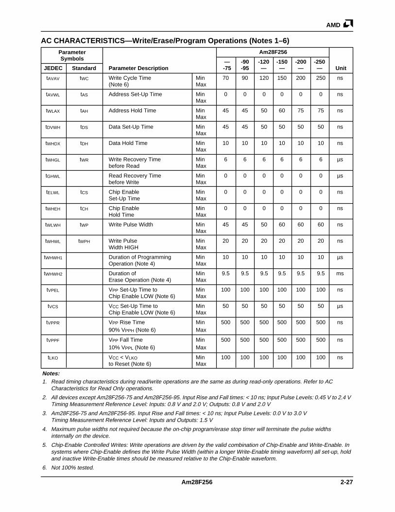
AC CHARACTERISTICS—Write/Erase/Program Operations (Notes 1–6)
— -90 -120 -150 -200 -250JEDEC Standard Parameter Description -75 -95 — — — — Unit
tAVAV tWC Write Cycle Time Min 70 90 120 150 200 250 ns(Note 6) Max
tAVWL tAS Address Set-Up Time Min 0 0 0 0 0 0 nsMax
tWLAX tAH Address Hold Time Min 45 45 50 60 75 75 nsMax
tDVWH tDS Data Set-Up Time Min 45 45 50 50 50 50 nsMax
tWHDX tDH Data Hold Time Min 10 10 10 10 10 10 nsMax
tWHGL tWR Write Recovery Time Min 6 6 6 6 6 6 µsbefore Read Max
tGHWL Read Recovery Time Min 0 0 0 0 0 0 µsbefore Write Max
tELWL tCS Chip Enable Min 0 0 0 0 0 0 nsSet-Up Time Max
tWHEH tCH Chip Enable Min 0 0 0 0 0 0 nsHold Time Max
tWLWH tWP Write Pulse Width Min 45 45 50 60 60 60 nsMax
tWHWL tWPH Write Pulse Min 20 20 20 20 20 20 nsWidth HIGH Max
tWHWH1 Duration of Programming Min 10 10 10 10 10 10 µsOperation (Note 4) Max
tWHWH2 Duration of Min 9.5 9.5 9.5 9.5 9.5 9.5 msErase Operation (Note 4) Max
tVPEL VPP Set-Up Time to Min 100 100 100 100 100 100 nsChip Enable LOW (Note 6) Max
tVCS VCC Set-Up Time to Min 50 50 50 50 50 50 µsChip Enable LOW (Note 6) Max
tVPPR VPP Rise Time Min 500 500 500 500 500 500 ns90% VPPH (Note 6) Max
tVPPF VPP Fall Time Min 500 500 500 500 500 500 ns10% VPPL (Note 6) Max
tLKO VCC < VLKO Min 100 100 100 100 100 100 nsto Reset (Note 6) Max
ParameterSymbols
Am28F256
Notes:1. Read timing characteristics during read/write operations are the same as during read-only operations. Refer to AC
Characteristics for Read Only operations.
2. All devices except Am28F256-75 and Am28F256-95. Input Rise and Fall times: < 10 ns; Input Pulse Levels: 0.45 V to 2.4 VTiming Measurement Reference Level: Inputs: 0.8 V and 2.0 V; Outputs: 0.8 V and 2.0 V
3. Am28F256-75 and Am28F256-95. Input Rise and Fall times: < 10 ns; Input Pulse Levels: 0.0 V to 3.0 VTiming Measurement Reference Level: Inputs and Outputs: 1.5 V
4. Maximum pulse widths not required because the on-chip program/erase stop timer will terminate the pulse widthsinternally on the device.
5. Chip-Enable Controlled Writes: Write operations are driven by the valid combination of Chip-Enable and Write-Enable. Insystems where Chip-Enable defines the Write Pulse Width (within a longer Write-Enable timing waveform) all set-up, holdand inactive Write-Enable times should be measured relative to the Chip-Enable waveform.
6. Not 100% tested.

AMD
2-28 Am28F256
KEY TO SWITCHING WAVEFORMS
Must BeSteady
MayChangefrom H to L
MayChangefrom L to H
Does Not Apply
Don’t Care,Any ChangePermitted
Will BeSteady
Will BeChangingfrom H to L
Will Be Changing from L to H
Changing,StateUnknown
CenterLine is High-Impedance“Off” State
WAVEFORM INPUTS OUTPUTS
KS000010
SWITCHING WAVEFORMS
Addresses
CE (E)
OE (G)
WE (W)
Data (DQ)
5.0 VVCC
0 V11560F-14
Power-Up, StandbyDevice and
Address SelectionOutputsEnabled
DataValid Standby, Power-Down
Addresses Stable
High Z High Z
tWHGL
tAVQV (tACC)
tEHQZ
(tDF)
tGHQZ
(tDF)
tELQX (tLZ)
tGLQX (tOLZ)
tELQV (tCE)
tGLQV (tOE)
tAXQX (tOH)
Output Valid
tAVAV (tRC)
tVCS
Figure 6. AC Waveforms for Read Operations

AMD
2-29Am28F256
SWITCHING WAVEFORMS
DATA IN= 20H
DATA IN= 20H
DATA IN= A0H
VALID DATAOUT
Power-Up &Standby
Set-Up EraseCommand Erase Command Erasure
Erase-VerifyCommand
Erase Verification
Standby/Power-Down
tAVAV(tWC)
tAVWL(tAS) tWLAX(tAH)
tELWL(tCS)tWHEH(tCH)
tEHQZ(tDF)
tGHWL(tOES)
tWHWH2
tWHGL
tGHQZ(tDF)
tWLWH(tWP)tDVWH(tDS)
tGLQX(tOLZ)
tGLQV(tOE)
tVPEL
Addresses
CE (E)
tELQV (tCE)
OE (G)
WE (W)
Data (DQ)
5.0 VVCC
0 V
VPPH
VPP
VPPL
11560F-15
tELQX (tLZ)
HIGH ZtWHDX(tDH)
tAVAV(tRC)
tWHWL(tWPH)
tAXQX(tOH)
tVCS
Figure 7. AC Waveforms for Erase Operations
AMD
2-30 Am28F256
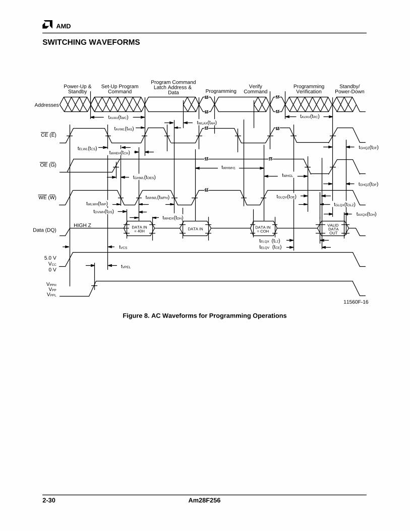
SWITCHING WAVEFORMS
DATA IN= 40H DATA IN DATA IN
= COH
VALID DATAOUT
Power-Up &Standby
Set-Up ProgramCommand
Program CommandLatch Address &
Data ProgrammingVerify
CommandProgrammingVerification
Standby/Power-Down
tAVAV(tWC)
tELWL(tCS)
tGHWL(tOES)
tWHWH1
tWHGL
tGHQZ(tDF)
tWLWH(tWP)
tDVWH(tDS)tWHDX(tDH)
tGLQX(tOLZ)
tGLQV(tOE)
tVPEL
Addresses
CE (E)
tELQV (tCE)
OE (G)
WE (W)
Data (DQ)
5.0 VVCC
0 V
VPPH
VPP
VPPL
11560F-16
tELQX (tLZ)
HIGH Z
tAVWL(tAS)tWLAX(tAH)
tGHQZ(tDF)tWHEH(tCH)
tAVAV(tRC)
tAXQX(tOH)
tWHWL(tWPH)
tVCS
Figure 8. AC Waveforms for Programming Operations
AMD
2-31Am28F256
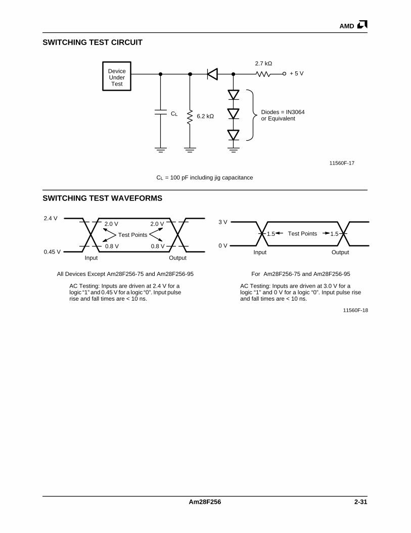
SWITCHING TEST CIRCUIT
DeviceUnderTest
CL
+ 5 V
CL = 100 pF including jig capacitance
6.2 kΩ
2.7 kΩ
Diodes = IN3064or Equivalent
11560F-17
SWITCHING TEST WAVEFORMS
AC Testing: Inputs are driven at 2.4 V for alogic “1” and 0.45 V for a logic “0”. Input pulserise and fall times are < 10 ns.
11560F-18
Test Points1.5 1.5
Input Output
3 V
0 V
AC Testing: Inputs are driven at 3.0 V for alogic “1” and 0 V for a logic “0”. Input pulse riseand fall times are < 10 ns.
All Devices Except Am28F256-75 and Am28F256-95 For Am28F256-75 and Am28F256-95
2.4 V
0.45 V
2.0 V
0.8 V
Test Points
2.0 V
0.8 V
Input Output

AMD
2-32 Am28F256
ERASE AND PROGRAMMING PERFORMANCE
Parameter Max Unit CommentsMin Typ (Note 3)
Chip Erase Time 1 10 sec Excludes 00H programming (Note 1) (Note 2) prior to erasure
Chip Programming Time 0.5 3 sec Excludes system-level overhead (Note 1)
Write/Erase Cycles 10,000 Cycles
Limits
Notes:
1. 25°C, 12 V VPP
2. The Flasherase/Flashrite algorithms allows for 60 second erase time for military temperature range operations.
3. Maximum time specified is lower than worst case. Worst case is derived from the Flasherase/Flashrite pulse count(Flasherase = 1000 max and Flashrite = 25 max). Typical worst case for program and erase operations is significantlyless than the actual device limit.
LATCHUP CHARACTERISTICS
Min Max
Input Voltage with respect to VSS on all pins except I/O pins(Including A9 and VPP) –1.0 V 13.5 V
Input Voltage with respect to VSS on all pins I/O pins –1.0 V VCC + 1.0 V
Current –100 mA +100 mA
Includes all pins except VCC. Test conditions: VCC = 5.0 V, one pin at a time.
DATA RETENTION
Parameter Test Conditions Min Unit
Minimum Pattern Data Retention Time 150°C 10 Years
125°C 20 Years
AMD
2-33Am28F256
DATA SHEET REVISION SUMMARY FORAm28F256Distinctive Characteristics, General Description,Connection Diagrams, and Ordering Information
Deleted references to ceramic packages, these will nolonger be available.
Pin Description
Added Output Enable high and Write Enable highdefinitions.
Basic Principles – Low V CC Write Inhibit
Clarified relationship between VCC and VLKO.
Table 1 – User Bus Operations
Added minimum rise time and fall time specifications toNote 7. Added Note 8.
Power-Up/Power-Down Sequence
Now includes power down requirements.
Table 4 – Flasherase Electrical Erase Algorithm
Note 1 – Changed to include AC characteristics.
Table 5 – Flashrite Programming Algorithm
Note 1 – Changed to include AC characteristics.
Absolute Maximum Ratings
Changed to reflect currently available packages; cor-rected errors in the notes.
DC Characteristics – TTL/NMOS and CMOSCompatible
Changed typical current for ICC1, ICC2, and ICC3 to 20 mA.Added 3.7 Volt typical specification to VLKO.
Note 1 – Added information to cautionary statement.