dmt038q2ntnt0-1a produt speifiation · 5710390642 dmt038q2ntnt0-1a product spe v0.1 ©2019...
TRANSCRIPT
©2019 Densitron Technologies Ltd.
TFT LCD Module
DMT038Q2NTNT0-1A
PRODUCT SPECIFICATION
Version 0.1
Dec 03, 2019 TBD
Customer’s Approval
Signature Date
Prepared by Chi Huang
Approved by Isaac Huang & Eric Wan
©2019 Densitron Technologies Ltd. Page 2 of 33 5710390642 DMT038Q2NTNT0-1A Product SPEC v0.1
TFT LCD Module
Revision History VERSION DATE DESCRIPTION AUTHOR
0.1 Dec 03, 2019 Preliminary Erica Cheng
Legal Notice Copyright ©2019 Densitron Technologies Ltd
All information contained in this document is proprietary and confidential to Densitron Technologies Ltd and is subject to a non-disclosure agreement. Unauthorized use, duplication, modification or disclosure of this information by any means without prior consent of Densitron Technologies Ltd is prohibited.
Every effort has been made to ensure the accuracy of this document; however, Densitron Technologies Ltd accepts no responsibility for any inaccuracies, errors or omissions herein. Densitron Technologies Ltd reserves the right to change specifications without prior notice in its absolute discretion, to supply the best product possible. Where Densitron Technologies Ltd or any of its group companies has (i) made a change to a product to incorporate a specific customer requirement or (ii) has created a design to a customer’s specific requirements, in either case the customer will indemnify and hold the relevant Densitron entity harmless against any claim that delivery against such requirement breaches any intellectual property or other rights of any 3rd party.
All brands and trademarks are the property of their respective owners and are hereby fully acknowledged.
©2019 Densitron Technologies Ltd. Page 3 of 33 5710390642 DMT038Q2NTNT0-1A Product SPEC v0.1
TFT LCD Module
Table of Contents GENERAL DESCRIPTION ......................................................................................................................................... 5
1.1 Introduction .................................................................................................................................................. 5
1.2 Main Features ............................................................................................................................................... 5
MECHANICAL SPECIFICATION ................................................................................................................................ 6
2.1 Mechanical Characteristics ........................................................................................................................... 6
2.2 Mechanical Drawing ...................................................................................................................................... 7
ELECTRICAL SPECIFICATION ................................................................................................................................... 8
3.1 Absolute Maximum Ratings .......................................................................................................................... 8
3.2 Electrical Characteristics ............................................................................................................................... 8
3.3 Interface Pin Assignment .............................................................................................................................. 9
3.4 Block Diagram ............................................................................................................................................. 10
3.5 Timing Characteristics ................................................................................................................................. 11
OPTICAL SPECIFICATION ...................................................................................................................................... 19
4.1 Optical Characteristics ................................................................................................................................ 19
LED BACKLIGHT SPECIFICATION ........................................................................................................................... 22
5.1 LED Backlight Characteristics ...................................................................................................................... 22
5.2 INTERNAL CIRCUIT DIAGRAM ..................................................................................................................... 22
PACKAGING ......................................................................................................................................................... 23
QUALITY ASSURANCE SPECIFICATION .................................................................................................................. 24
7.1 Conformity .................................................................................................................................................. 24
7.2 Environment Required ................................................................................................................................ 24
7.3 Delivery Assurance ...................................................................................................................................... 24
7.4 Dealing with Customer Complaints ............................................................................................................. 29
RELIABILITY SPECIFICATION ................................................................................................................................. 30
8.1 Reliability Tests ............................................................................................................................................ 30
HANDLING PRECAUTIONS.................................................................................................................................... 31
9.1 Handling Precautions .................................................................................................................................. 31
9.2 Storage Precautions .................................................................................................................................... 32
9.3 Designing Precautions ................................................................................................................................. 32
©2019 Densitron Technologies Ltd. Page 4 of 33 5710390642 DMT038Q2NTNT0-1A Product SPEC v0.1
TFT LCD Module
9.4 Operation Precautions ................................................................................................................................ 33
9.5 Other Precautions ....................................................................................................................................... 33
©2019 Densitron Technologies Ltd. Page 5 of 33 5710390642 DMT038Q2NTNT0-1A Product SPEC v0.1
TFT LCD Module
General Description
1.1 Introduction
This is a 3.83” size colour active matrix TFT LCD module with glare polarizer that uses amorphous silicon TFT as a
switching device. The display is normally white mode, transmissive, and featuring high contrast and excellent colour
saturation. The resolution of the TFT-LCD is 480 x 110 and can display up to 16M colours. The display module supports
24-bits RGB interface.
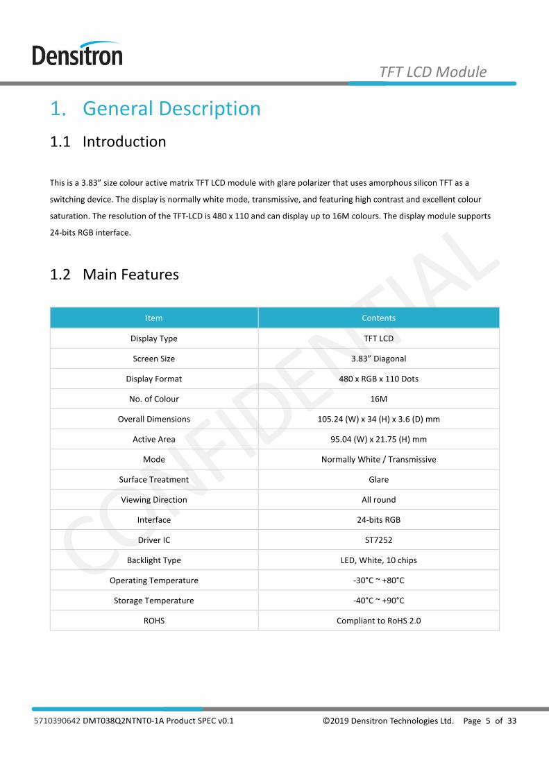
1.2 Main Features
Item Contents
Display Type TFT LCD
Screen Size 3.83” Diagonal
Display Format 480 x RGB x 110 Dots
No. of Colour 16M
Overall Dimensions 105.24 (W) x 34 (H) x 3.6 (D) mm
Active Area 95.04 (W) x 21.75 (H) mm
Mode Normally White / Transmissive
Surface Treatment Glare
Viewing Direction All round
Interface 24-bits RGB
Driver IC ST7252
Backlight Type LED, White, 10 chips
Operating Temperature -30°C ~ +80°C
Storage Temperature -40°C ~ +90°C
ROHS Compliant to RoHS 2.0
©2019 Densitron Technologies Ltd. Page 6 of 33 5710390642 DMT038Q2NTNT0-1A Product SPEC v0.1
TFT LCD Module
Mechanical Specification
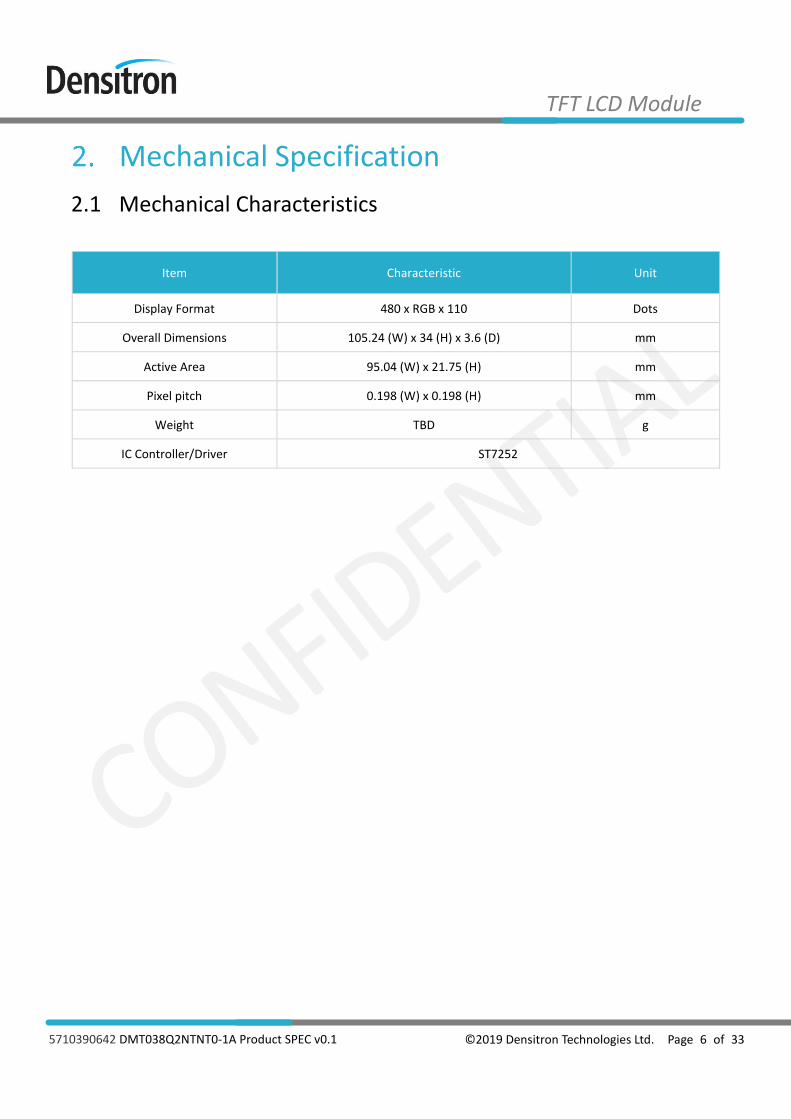
2.1 Mechanical Characteristics
Item Characteristic Unit
Display Format 480 x RGB x 110 Dots
Overall Dimensions 105.24 (W) x 34 (H) x 3.6 (D) mm
Active Area 95.04 (W) x 21.75 (H) mm
Pixel pitch 0.198 (W) x 0.198 (H) mm
Weight TBD g
IC Controller/Driver ST7252
©2019 Densitron Technologies Ltd. Page 7 of 33 5710390642 DMT038Q2NTNT0-1A Product SPEC v0.1
TFT LCD Module
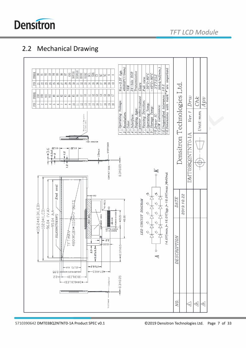
2.2 Mechanical Drawing

©2019 Densitron Technologies Ltd. Page 8 of 33 5710390642 DMT038Q2NTNT0-1A Product SPEC v0.1
TFT LCD Module
Electrical Specification
3.1 Absolute Maximum Ratings
AGND = GND = 0V, Ta = 25°C
Item Symbol Min Max Unit Note
Power Voltage VCC -0.3 4.6 V -
Operating Temperature TOPR -30 80 °C 2, 3
Storage Temperature TSTG -40 90 °C 2, 3
Note 1: When this module is used beyond the above absolute maximum ratings, permanent breakage of the module
may occur. For normal operations, it is desirable to use this module under the conditions according to Section
3.2 “Electrical Characteristics”, to avoid malfunctioning.
Note 2: Background colour changes slightly depending on ambient temperature. This phenomenon is reversible.
Note 3: Please refer to item of RELIABILITY.
3.2 Electrical Characteristics
AGND = GND = 0V, Ta = 25°C
Item Symbol Condition Min Typ Max Unit Note
Power Voltage VCC - 3.0 3.3 3.6 V -
Input Logic High Voltage VIH - 0.7 VCC - VCC V -
Input Logic Low Voltage VIL - 0 - 0.3 VCC V -
©2019 Densitron Technologies Ltd. Page 9 of 33 5710390642 DMT038Q2NTNT0-1A Product SPEC v0.1
TFT LCD Module
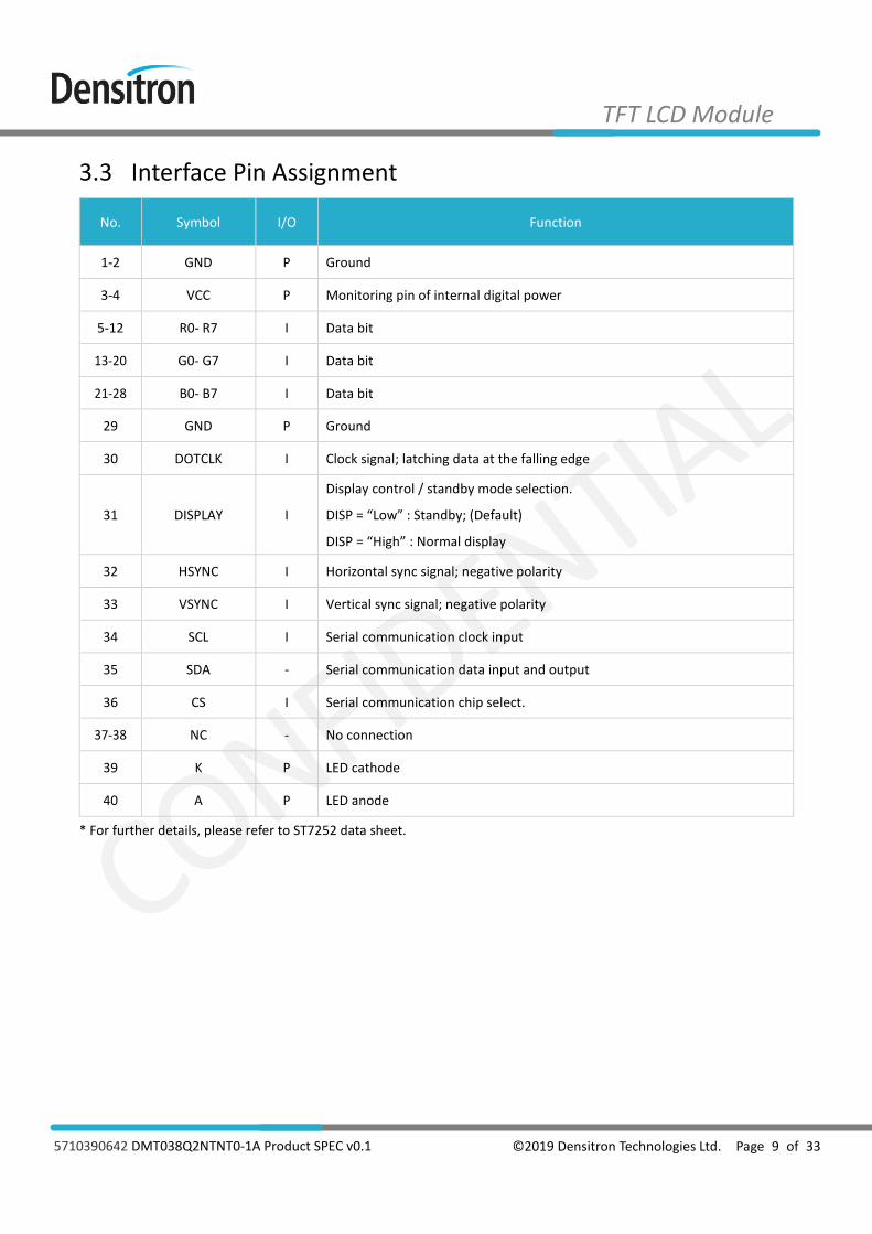
3.3 Interface Pin Assignment
No. Symbol I/O Function
1-2 GND P Ground
3-4 VCC P Monitoring pin of internal digital power
5-12 R0- R7 I Data bit
13-20 G0- G7 I Data bit
21-28 B0- B7 I Data bit
29 GND P Ground
30 DOTCLK I Clock signal; latching data at the falling edge
31 DISPLAY I
Display control / standby mode selection.
DISP = “Low” : Standby; (Default)
DISP = “High” : Normal display
32 HSYNC I Horizontal sync signal; negative polarity
33 VSYNC I Vertical sync signal; negative polarity
34 SCL I Serial communication clock input
35 SDA - Serial communication data input and output
36 CS I Serial communication chip select.
37-38 NC - No connection
39 K P LED cathode
40 A P LED anode
* For further details, please refer to ST7252 data sheet.
©2019 Densitron Technologies Ltd. Page 10 of 33 5710390642 DMT038Q2NTNT0-1A Product SPEC v0.1
TFT LCD Module
3.4 Block Diagram
TBD
©2019 Densitron Technologies Ltd. Page 11 of 33 5710390642 DMT038Q2NTNT0-1A Product SPEC v0.1
TFT LCD Module
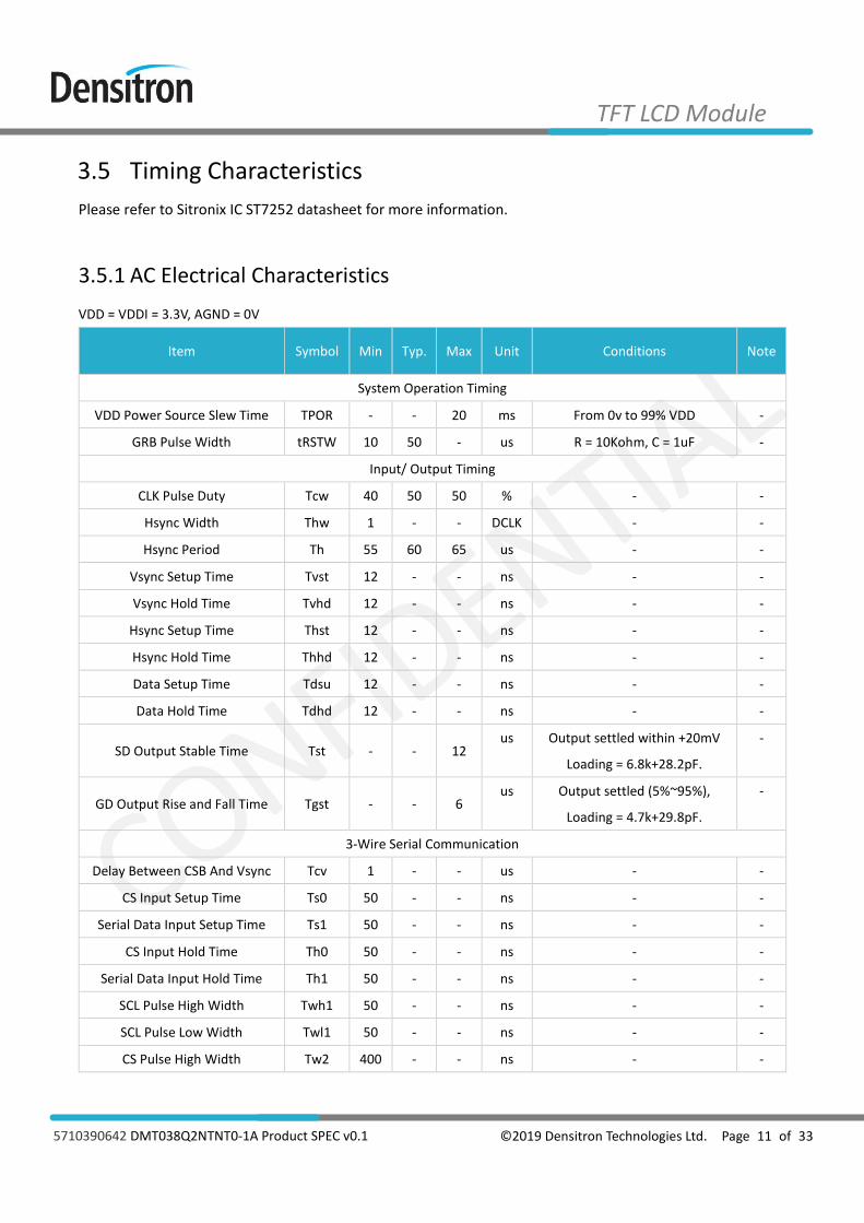
3.5 Timing Characteristics
Please refer to Sitronix IC ST7252 datasheet for more information.
3.5.1 AC Electrical Characteristics
VDD = VDDI = 3.3V, AGND = 0V
Item Symbol Min Typ. Max Unit Conditions Note
System Operation Timing
VDD Power Source Slew Time TPOR - - 20 ms From 0v to 99% VDD -
GRB Pulse Width tRSTW 10 50 - us R = 10Kohm, C = 1uF -
Input/ Output Timing
CLK Pulse Duty Tcw 40 50 50 % - -
Hsync Width Thw 1 - - DCLK - -
Hsync Period Th 55 60 65 us - -
Vsync Setup Time Tvst 12 - - ns - -
Vsync Hold Time Tvhd 12 - - ns - -
Hsync Setup Time Thst 12 - - ns - -
Hsync Hold Time Thhd 12 - - ns - -
Data Setup Time Tdsu 12 - - ns - -
Data Hold Time Tdhd 12 - - ns - -
SD Output Stable Time Tst - - 12 us Output settled within +20mV
Loading = 6.8k+28.2pF.
-
GD Output Rise and Fall Time Tgst - - 6 us Output settled (5%~95%),
Loading = 4.7k+29.8pF.
-
3-Wire Serial Communication
Delay Between CSB And Vsync Tcv 1 - - us - -
CS Input Setup Time Ts0 50 - - ns - -
Serial Data Input Setup Time Ts1 50 - - ns - -
CS Input Hold Time Th0 50 - - ns - -
Serial Data Input Hold Time Th1 50 - - ns - -
SCL Pulse High Width Twh1 50 - - ns - -
SCL Pulse Low Width Twl1 50 - - ns - -
CS Pulse High Width Tw2 400 - - ns - -
©2019 Densitron Technologies Ltd. Page 12 of 33 5710390642 DMT038Q2NTNT0-1A Product SPEC v0.1
TFT LCD Module
3.5.2 DC Electrical Characteristics
Item Symbol Min Typ. Max Unit Conditions Note
Recommended Operating Range
System Voltage VDD 3.0 3.3 3.6 V - -
IO System Voltage VDDI 1.65 - VDD V - -
Charge Pump System Voltage PVDD 3.0 3.3 3.6 V - -
NVM System Voltage VPP 7.4 7.5 7.6 V - -
DC Characteristics for Digital Circuit
Logic-High Input Voltage Vih 0.7 VDDI - VDDI V VDDI = 3.3V -
Logic-Low Input Voltage Vil DGND - 0.3 VDDI V VDDI = 3.3V -
Logic-High Output Voltage Voh VDDI-0.4 - VDDI V VDDI = 3.3V -
Logic-Low Output Voltage Vol DGND - DGND+0.4 V VDDI = 3.3V -
DC Characteristics for Analog Circuit
Positive High-Voltage Power VGH 13 15 16 V PVDD = 3.3V -
Negative High-Voltage Power VGL -10 -10 -7 V PVDD = 3.3V -
Output Voltage Deviation Vod - ±35 ±45 mV - -
Standby Current Isc - - 50 uA VDD = PVDD = 3.3V -
Operation Current Ioc - 20 - mA
No Load,
VDD = PVDD = 3.3V
@ FR=60Hz
-
©2019 Densitron Technologies Ltd. Page 13 of 33 5710390642 DMT038Q2NTNT0-1A Product SPEC v0.1
TFT LCD Module
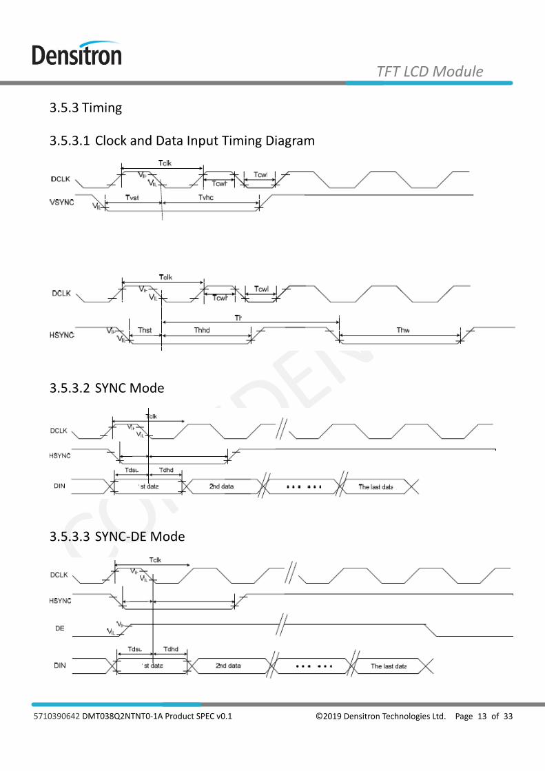
3.5.3 Timing
3.5.3.1 Clock and Data Input Timing Diagram
3.5.3.2 SYNC Mode
3.5.3.3 SYNC-DE Mode
©2019 Densitron Technologies Ltd. Page 14 of 33 5710390642 DMT038Q2NTNT0-1A Product SPEC v0.1
TFT LCD Module
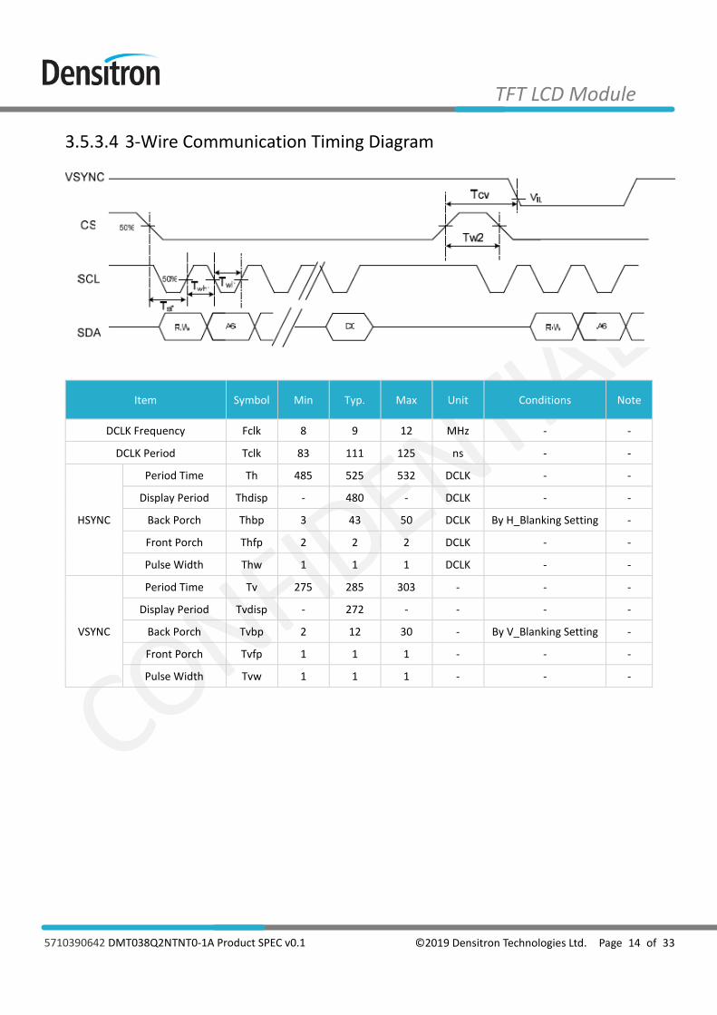
3.5.3.4 3-Wire Communication Timing Diagram
Item Symbol Min Typ. Max Unit Conditions Note
DCLK Frequency Fclk 8 9 12 MHz - -
DCLK Period Tclk 83 111 125 ns - -
HSYNC
Period Time Th 485 525 532 DCLK - -
Display Period Thdisp - 480 - DCLK - -
Back Porch Thbp 3 43 50 DCLK By H_Blanking Setting -
Front Porch Thfp 2 2 2 DCLK - -
Pulse Width Thw 1 1 1 DCLK - -
VSYNC
Period Time Tv 275 285 303 - - -
Display Period Tvdisp - 272 - - - -
Back Porch Tvbp 2 12 30 - By V_Blanking Setting -
Front Porch Tvfp 1 1 1 - - -
Pulse Width Tvw 1 1 1 - - -
©2019 Densitron Technologies Ltd. Page 15 of 33 5710390642 DMT038Q2NTNT0-1A Product SPEC v0.1
TFT LCD Module
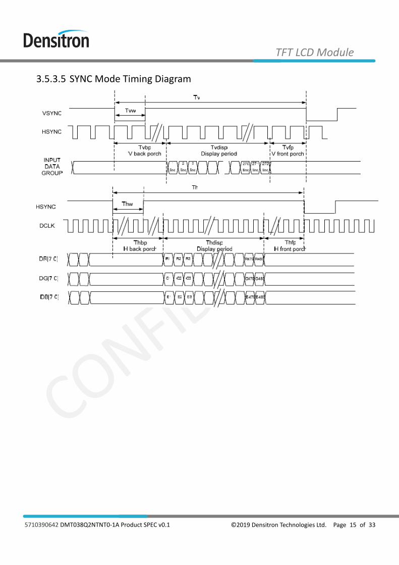
3.5.3.5 SYNC Mode Timing Diagram
©2019 Densitron Technologies Ltd. Page 16 of 33 5710390642 DMT038Q2NTNT0-1A Product SPEC v0.1
TFT LCD Module
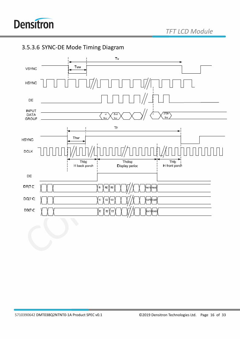
3.5.3.6 SYNC-DE Mode Timing Diagram
©2019 Densitron Technologies Ltd. Page 17 of 33 5710390642 DMT038Q2NTNT0-1A Product SPEC v0.1
TFT LCD Module
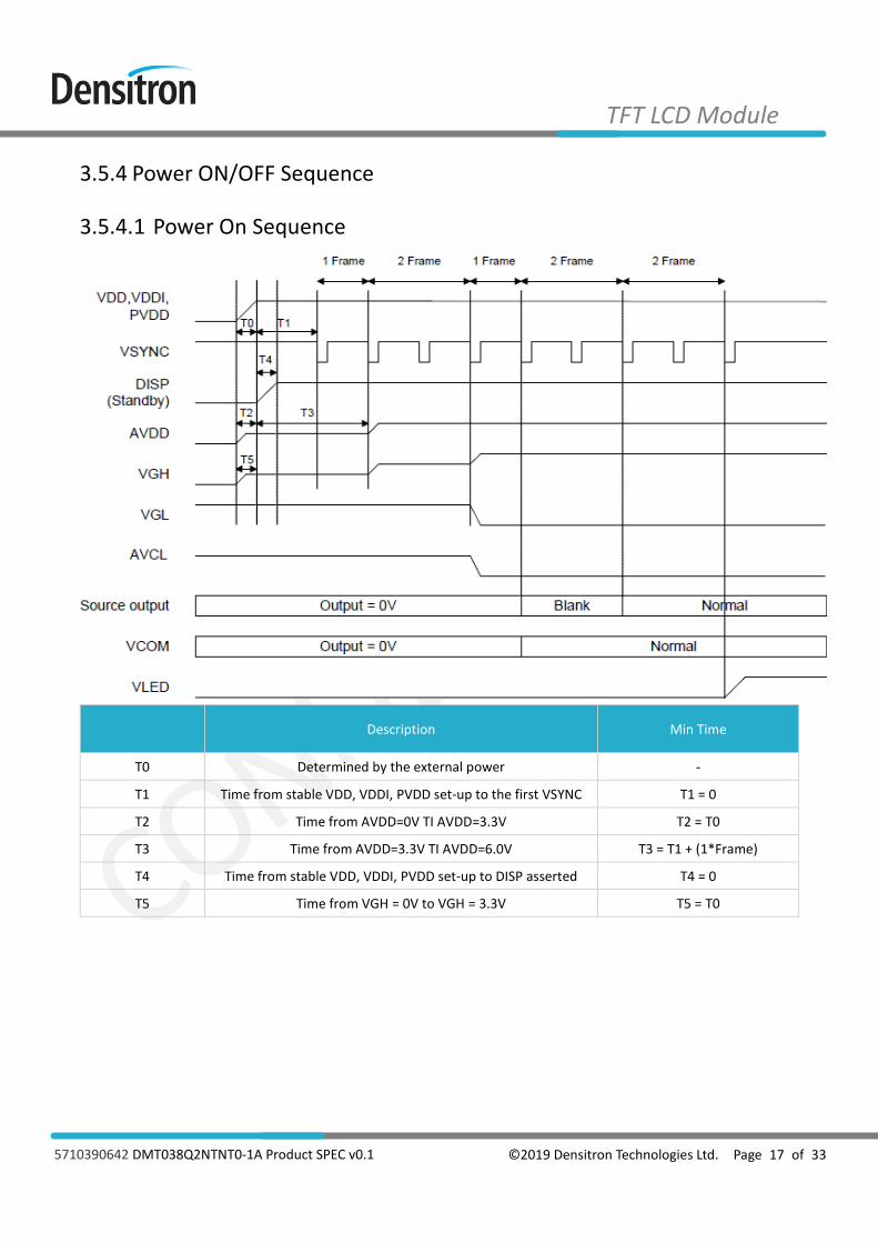
3.5.4 Power ON/OFF Sequence
3.5.4.1 Power On Sequence
Description Min Time
T0 Determined by the external power -
T1 Time from stable VDD, VDDI, PVDD set-up to the first VSYNC T1 = 0
T2 Time from AVDD=0V TI AVDD=3.3V T2 = T0
T3 Time from AVDD=3.3V TI AVDD=6.0V T3 = T1 + (1*Frame)
T4 Time from stable VDD, VDDI, PVDD set-up to DISP asserted T4 = 0
T5 Time from VGH = 0V to VGH = 3.3V T5 = T0
©2019 Densitron Technologies Ltd. Page 18 of 33 5710390642 DMT038Q2NTNT0-1A Product SPEC v0.1
TFT LCD Module
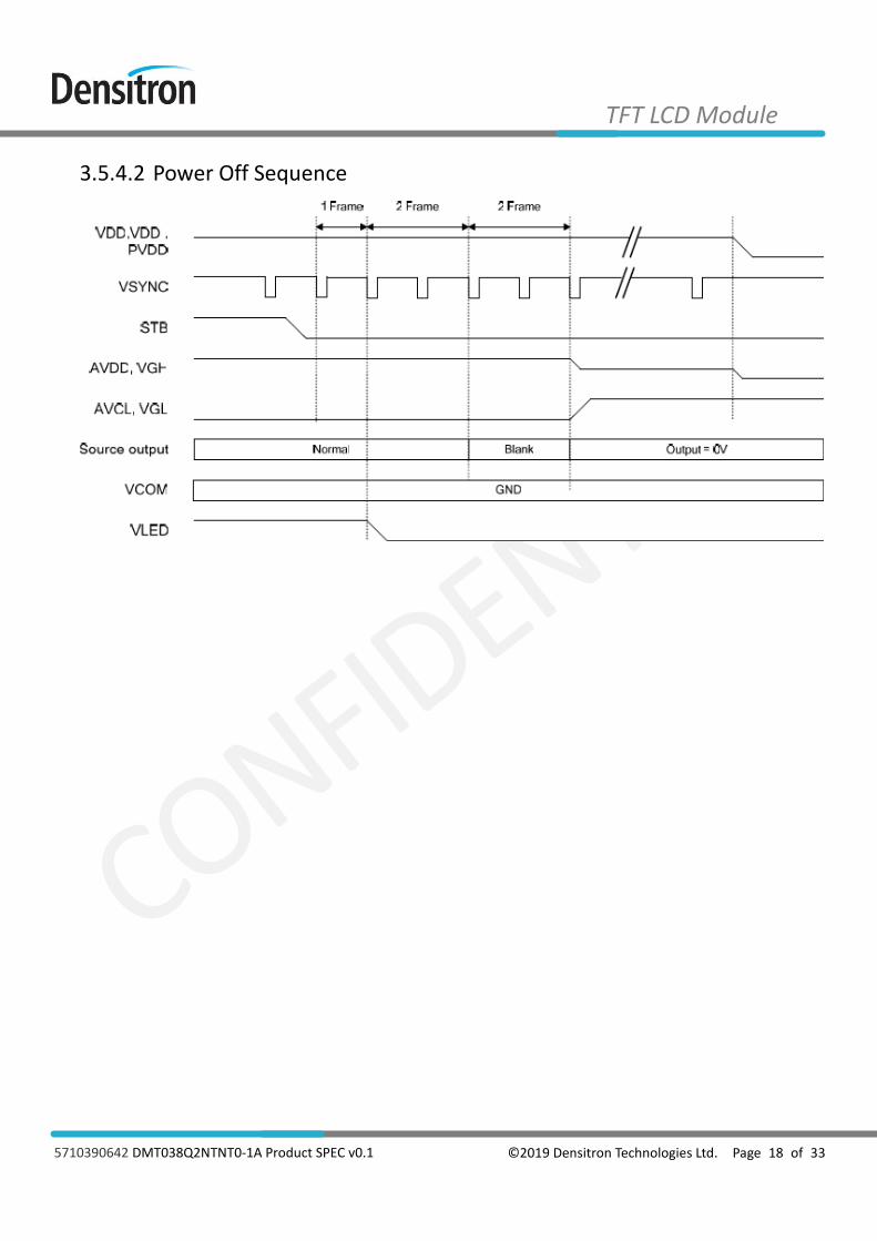
3.5.4.2 Power Off Sequence
©2019 Densitron Technologies Ltd. Page 19 of 33 5710390642 DMT038Q2NTNT0-1A Product SPEC v0.1
TFT LCD Module
Optical Specification
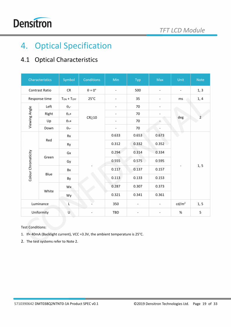
4.1 Optical Characteristics
Characteristics Symbol Conditions Min Typ Max Unit Note
Contrast Ratio CR = 0° - 500 - - 1, 3
Response time TON + TOFF 25°C - 35 - ms 1, 4
Vie
win
g A
ngl
e Left x-
CR≧10
- 70 -
deg 2 Right x+ - 70 -
Up Y+ - 70 -
Down Y- - 70 -
Co
lou
r C
hro
mat
icit
y
Red Rx
-
0.633 0.653 0.673
- 1, 5
Ry 0.312 0.332 0.352
Green Gx 0.294 0.314 0.334
Gy 0.555 0.575 0.595
Blue Bx 0.117 0.137 0.157
By 0.113 0.133 0.153
White Wx 0.287 0.307 0.373
Wy 0.321 0.341 0.361
Luminance L - 350 - - cd/m2 1, 5
Uniformity U - TBD - - % 5
Test Conditions:
1. If= 40mA (Backlight current), VCC =3.3V, the ambient temperature is 25°C.
2. The test systems refer to Note 2.

©2019 Densitron Technologies Ltd. Page 20 of 33 5710390642 DMT038Q2NTNT0-1A Product SPEC v0.1
TFT LCD Module
Note Item Test method
1
Definition of Optical
Measurement
System
The optical characteristics should be measured in dark room. After 5-Minutes
operation, the optical properties are measured at the center point of the LCD
screen. All input terminals LCD panel must be grounded when measuring the center
area of the panel.
2 Definition of Viewing
Angle (x, y)
3 Definition of Contrast
Ratio (CR)
4
Definition of
Response Time
(TON, TOFF)
The response time is defined as the LCD optical switching time interval between “White”state and “Black” state. Rise time (TON)is the time between photo detector output intensity changed from 90% to 10%. and fall time (TOFF)is the time between photo detector output intensity changed from 10% to90%.
©2019 Densitron Technologies Ltd. Page 21 of 33 5710390642 DMT038Q2NTNT0-1A Product SPEC v0.1
TFT LCD Module
Note Item Test method
5
Definition of Color
Chromaticity
(CIE1931)
Color coordinates measured at center point of LCD.
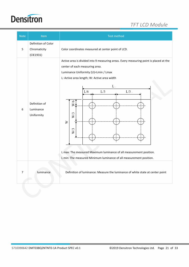
6
Definition of
Luminance
Uniformity
Active area is divided into 9 measuring areas. Every measuring point is placed at the
center of each measuring area.
Luminance Uniformity (U)=Lmin / Lmax
L: Active area length; W: Active area width
L max: The measured Maximum luminance of all measurement position.
L min: The measured Minimum luminance of all measurement position.
7 luminance Definition of luminance: Measure the luminance of white state at center point

©2019 Densitron Technologies Ltd. Page 22 of 33 5710390642 DMT038Q2NTNT0-1A Product SPEC v0.1
TFT LCD Module
LED Backlight Specification
5.1 LED Backlight Characteristics
(Ta = 25°C)
Item Symbol Condition Min Typ Max Unit Note
Forward Voltage Vf - 14 16 18 V -
Forward Current If - - 40 - mA -
Operating Life Time - - 36000 - - Hours -
Note 1: Ta means ambient temperature of TFT-LCD module.
Note 2: IF, VF are defined for one channel LED. There are two LED channel in back light unit.
Note 3: If the module is driven by high current or at high ambient temperature & humidity condition. The operating life
will be reduced.
Note 4: Operating life means brightness goes down to 50% initial brightness. Minimum operating life time is estimated
data.
5.2 INTERNAL CIRCUIT DIAGRAM
©2019 Densitron Technologies Ltd. Page 23 of 33 5710390642 DMT038Q2NTNT0-1A Product SPEC v0.1
TFT LCD Module
Packaging TBD
©2019 Densitron Technologies Ltd. Page 24 of 33 5710390642 DMT038Q2NTNT0-1A Product SPEC v0.1
TFT LCD Module
Quality Assurance Specification
7.1 Conformity
The performance, function and reliability of the shipped products conform to the Product Specification.
7.2 Environment Required
Customer’s test & measurement are required to be conducted under the following conditions:
Temperature: 25 ± 5C
Humidity: 60% ± 10% RH
Illumination: under 40W fluorescent light
Viewing distance: 30 ± 10cm
Finger glove (or finger cover) must be worn by the inspector.
Inspection table or jig must be anti-electrostatic.
7.3 Delivery Assurance
7.3.1 Delivery Inspection Standards
Inspection Level II, GB2828-87
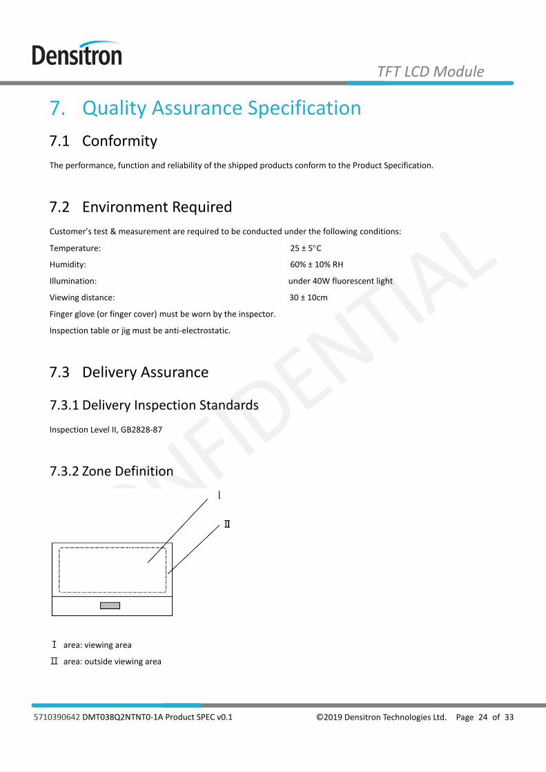
7.3.2 Zone Definition
Ⅰ area: viewing area
Ⅱ area: outside viewing area
©2019 Densitron Technologies Ltd. Page 25 of 33 5710390642 DMT038Q2NTNT0-1A Product SPEC v0.1
TFT LCD Module
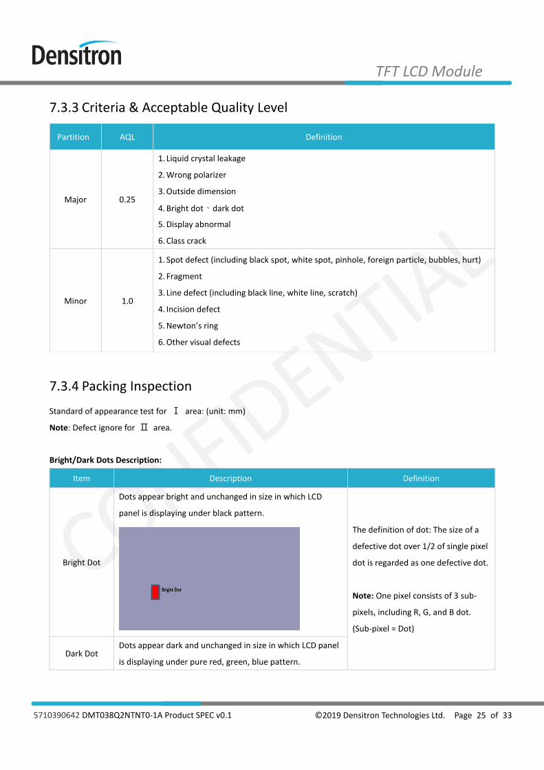
7.3.3 Criteria & Acceptable Quality Level
7.3.4 Packing Inspection
Standard of appearance test for Ⅰ area: (unit: mm)
Note: Defect ignore for Ⅱ area.
Bright/Dark Dots Description:
Item Description Definition
Bright Dot
Dots appear bright and unchanged in size in which LCD
panel is displaying under black pattern.
The definition of dot: The size of a
defective dot over 1/2 of single pixel
dot is regarded as one defective dot.
Note: One pixel consists of 3 sub-
pixels, including R, G, and B dot.
(Sub-pixel = Dot)
Dark Dot Dots appear dark and unchanged in size in which LCD panel
is displaying under pure red, green, blue pattern.
Partition AQL Definition
Major 0.25
1. Liquid crystal leakage
2. Wrong polarizer
3. Outside dimension
4. Bright dot、dark dot
5. Display abnormal
6. Class crack
Minor 1.0
1. Spot defect (including black spot, white spot, pinhole, foreign particle, bubbles, hurt)
2. Fragment
3. Line defect (including black line, white line, scratch)
4. Incision defect
5. Newton’s ring
6. Other visual defects
©2019 Densitron Technologies Ltd. Page 26 of 33 5710390642 DMT038Q2NTNT0-1A Product SPEC v0.1
TFT LCD Module
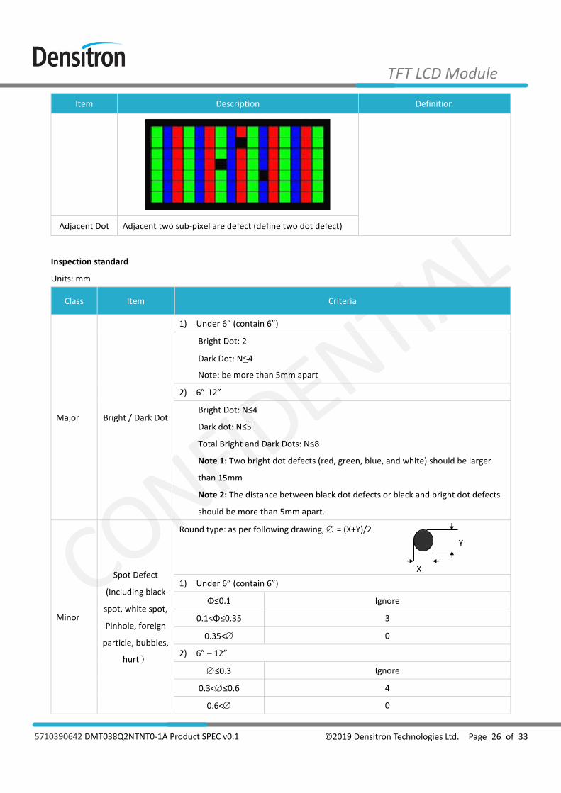
Item Description Definition
Adjacent Dot Adjacent two sub-pixel are defect (define two dot defect)
Inspection standard
Units: mm
Class Item Criteria
Major Bright / Dark Dot
1) Under 6” (contain 6”)
Bright Dot: 2
Dark Dot: N≦4
Note: be more than 5mm apart
2) 6”-12”
Bright Dot: N≤4
Dark dot: N≤5
Total Bright and Dark Dots: N≤8
Note 1: Two bright dot defects (red, green, blue, and white) should be larger
than 15mm
Note 2: The distance between black dot defects or black and bright dot defects
should be more than 5mm apart.
Minor
Spot Defect
(Including black
spot, white spot,
Pinhole, foreign
particle, bubbles,
hurt)
Round type: as per following drawing, = (X+Y)/2
1) Under 6” (contain 6”)
Φ≤0.1 Ignore
0.1<Φ≤0.35 3
0.35< 0
2) 6” – 12”
≤0.3 Ignore
0.3<≤0.6 4
0.6< 0
X
Y
©2019 Densitron Technologies Ltd. Page 27 of 33 5710390642 DMT038Q2NTNT0-1A Product SPEC v0.1
TFT LCD Module
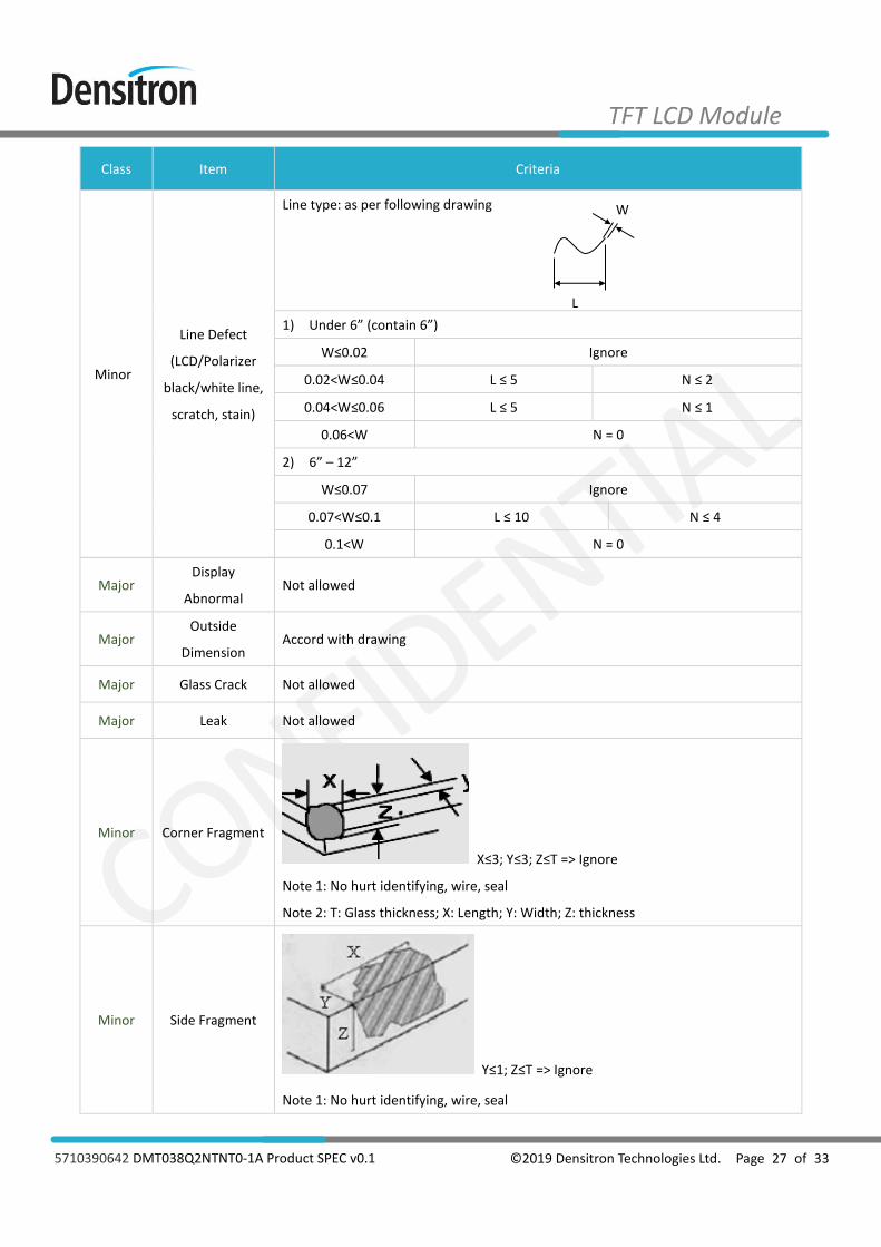
Class Item Criteria
Minor
Line Defect
(LCD/Polarizer
black/white line,
scratch, stain)
Line type: as per following drawing
1) Under 6” (contain 6”)
W≤0.02 Ignore
0.02<W≤0.04 L ≤ 5 N ≤ 2
0.04<W≤0.06 L ≤ 5 N ≤ 1
0.06<W N = 0
2) 6” – 12”
W≤0.07 Ignore
0.07<W≤0.1 L ≤ 10 N ≤ 4
0.1<W N = 0
Major Display
Abnormal Not allowed
Major Outside
Dimension Accord with drawing
Major Glass Crack Not allowed
Major Leak Not allowed
Minor Corner Fragment
X≤3; Y≤3; Z≤T => Ignore
Note 1: No hurt identifying, wire, seal
Note 2: T: Glass thickness; X: Length; Y: Width; Z: thickness
Minor Side Fragment
Y≤1; Z≤T => Ignore
Note 1: No hurt identifying, wire, seal
L
W
©2019 Densitron Technologies Ltd. Page 28 of 33 5710390642 DMT038Q2NTNT0-1A Product SPEC v0.1
TFT LCD Module
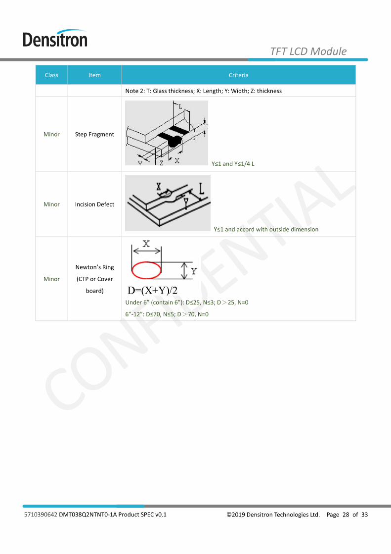
Class Item Criteria
Note 2: T: Glass thickness; X: Length; Y: Width; Z: thickness
Minor Step Fragment
Y≤1 and Y≤1/4 L
Minor Incision Defect
Y≤1 and accord with outside dimension
Minor
Newton’s Ring
(CTP or Cover
board)
Under 6” (contain 6”): D≤25, N≤3; D>25, N=0
6”-12”: D≤70, N≤5; D>70, N=0
©2019 Densitron Technologies Ltd. Page 29 of 33 5710390642 DMT038Q2NTNT0-1A Product SPEC v0.1
TFT LCD Module
7.4 Dealing with Customer Complaints
7.4.1 Non-conforming Analysis
Purchaser should supply Densitron with detailed data of non-conforming sample.
After accepting it, Densitron should complete the analysis in two weeks from receiving the sample.
If the analysis cannot be completed on time, Densitron must inform the purchaser.
7.4.2 Handling of Non-conforming Displays
If any non-conforming displays are found during customer acceptance inspection which Densitron is clearly responsible
for, return them to Densitron.
Both Densitron and customer should analyse the reason and discuss the handling of non-conforming displays when the
reason is not clear.
Equally, both sides should discuss and come to agreement for issues pertaining to modification of Densitron quality
assurance standard.
©2019 Densitron Technologies Ltd. Page 30 of 33 5710390642 DMT038Q2NTNT0-1A Product SPEC v0.1
TFT LCD Module
Reliability Specification
8.1 Reliability Tests
Test Item Test Condition Evaluation and assessment
High Temperature Operation 70 ± 2°C, 240 hrs
Inspection after 2~4hours
storage at room temperature,
the sample shall be free from
defects:
1) Air bubble in the LCD;
2) Sealleak;
3) Non-display;
4) missing segments;
5) Glass crack;
6) Current Idd is twice
higher than initial value.
Low Temperature Operation -20 ± 2°C, 240 hrs
High Temperature Storage 80 ± 2°C, 240 hrs
Low Temperature Storage -30 ± 2°C, 240 hrs
Temperature Cycle -40°C ~ 25°C ~ 90°C × 10 cycles
(30min.) (5min.) (30min.)
Damp Proof Test 40°C ± 5°C × 90%RH, 240 hrs
Vibration Test
Frequency: 10Hz~55Hz~10Hz
Amplitude: 1.5mm,
X, Y, Z direction for total 3 hours
(Packing condition)
Dropping Test Drop to the ground from 1m height, one time,
every side of carton. (Packing condition)
ESD test
Voltage: ±8KV R: 330Ω C: 150pF
Air discharge, 10time
Voltage: ±6KV R: 330Ω C: 150pF
Contact discharge, 10time
Note 1: The test samples should be applied to only one test item.
Note 2: Sample size for each test item is 5~10pcs.
Note 3: For Damp Proof Test, Pure water(Resistance>10MΩ) should be used.
Note 4: In case of malfunction defect caused by ESD damage, if it would be recovered to normal state after resetting, it
would be judge as a good part.
Note 5: Failure Judgment Criterion: Basic Specification, Electrical Characteristic, Mechanical Characteristic, Optical
Characteristic.
Note 6: Please use automatic switch menu (or roll menu) testing mode when test operating mode.
8.1.1 Inspection Check Standard
After the completion of the described reliability test, the samples are to be left at room temperature for 4 hrs prior to
conducting the inspection check at 23±5 °C, 55±15% RH.
©2019 Densitron Technologies Ltd. Page 31 of 33 5710390642 DMT038Q2NTNT0-1A Product SPEC v0.1
TFT LCD Module
Handling Precautions
9.1 Handling Precautions
1) Since the display panel is being made of glass, do not apply mechanical impacts such us dropping from a high
position.
2) If the display panel is broken by some accident and the internal organic substance leaks out, be careful not to
inhale nor lick the organic substance.
3) If the liquid crystal touches your skin or clothes, wash it off immediately using soap and plenty of water
4) If pressure is applied to the display surface or its neighbourhood of the display module, the cell structure may be
damaged and be careful not to apply pressure to these sections.
5) The polarizer covering the surface of the display module is soft and easily scratched. Please be careful when
handling the display module.
6) When the surface of the polarizer of the display module has soil, clean the surface. It takes advantage of by using
following adhesion tape.
a. Scotch Mending Tape No. 810 or an equivalent
b. Never try to breathe upon the soiled surface nor wipe the surface using cloth containing solvent such as ethyl
alcohol, since the surface of the polarizer will become cloudy.
c. Also, pay attention that the following liquid and solvent may spoil the polarizer:
• Water
• Ketone
• Aromatic Solvents
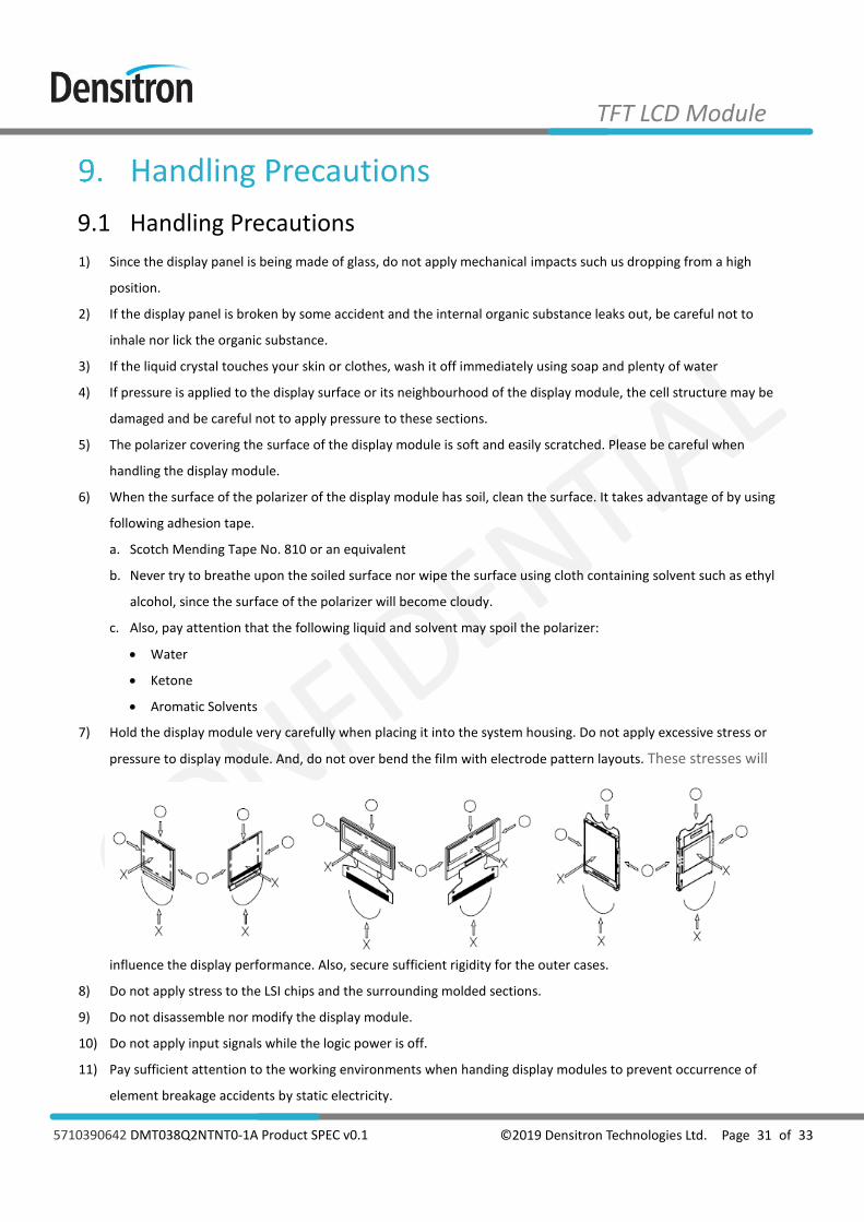
7) Hold the display module very carefully when placing it into the system housing. Do not apply excessive stress or
pressure to display module. And, do not over bend the film with electrode pattern layouts. These stresses will
influence the display performance. Also, secure sufficient rigidity for the outer cases.
8) Do not apply stress to the LSI chips and the surrounding molded sections.
9) Do not disassemble nor modify the display module.
10) Do not apply input signals while the logic power is off.
11) Pay sufficient attention to the working environments when handing display modules to prevent occurrence of
element breakage accidents by static electricity.
©2019 Densitron Technologies Ltd. Page 32 of 33 5710390642 DMT038Q2NTNT0-1A Product SPEC v0.1
TFT LCD Module
a. Be sure to make human body grounding when handling display modules.
b. Be sure to ground tools to use or assembly such as soldering irons.
c. To suppress generation of static electricity, avoid carrying out assembly work under dry environments.
d. Protective film is being applied to the surface of the display panel of the display module. Be careful since static
electricity may be generated when exfoliating the protective film.
12) Protection film is being applied to the surface of the display panel and removes the protection film before
assembling it. If the display module has been stored for a long period of time, residue adhesive material of the
protection film may remain on the surface of the display panel after removed of the film. In such case, remove the
residue material by the method introduced in the above Section 5).
13) If electric current is applied when the display module is being dewed or when it is placed under high humidity
environments, the electrodes may be corroded and be careful to avoid the above.
9.2 Storage Precautions
1) When storing display modules, put them in static electricity preventive bags avoiding exposure to direct sun light
nor to lights of fluorescent lamps, etc. and, also, avoiding high temperature and high humidity environments or
low temperature (less than 0°C) environments. (We recommend you to store these modules in the packaged state
when they were shipped from Densitron) At that time, be careful not to let water drops adhere to the packages or
bags nor let dewing occur with them.
2) If electric current is applied when water drops are adhering to the surface of the display module, when the display
module is being dewed or when it is placed under high humidity environments, the electrodes may be corroded
and be careful about the above.
9.3 Designing Precautions
1) The absolute maximum ratings are the ratings which cannot be exceeded for display module, and if these values
are exceeded, panel damage may be happen.
2) To prevent occurrence of malfunctioning by noise, pay attention to satisfy the VIL and VIH specifications and, at
the same time, to make the signal line cable as short as possible.
3) We recommend you to install excess current preventive unit (fuses, etc.) to the power circuit (VDD). (Recommend
value: 0.5A)
4) Pay sufficient attention to avoid occurrence of mutual noise interference with the neighbouring devices.
5) As for EMI, take necessary measures on the equipment side basically.
6) When fastening the display module, fasten the external plastic housing section.
7) If power supply to the display module is forcibly shut down by such errors as taking out the main battery while the
display panel is in operation, we cannot guarantee the quality of this display module.
©2019 Densitron Technologies Ltd. Page 33 of 33 5710390642 DMT038Q2NTNT0-1A Product SPEC v0.1
TFT LCD Module
9.4 Operation Precautions
1) It is indispensable to drive the display within the specified voltage limit since excessive voltage shortens its life.
2) Direct current causes an electrochemical reaction with remarkable deterioration of the display quality. Give
careful consideration to prevent direct current during ON/OFF timing and during operation.
3) Response time is extremely delayed at temperatures lower than the operating temperature range while, at high
temperatures, displays become dark. However, this phenomenon is reversible and does not mean a malfunction
or a display that has been permanently damaged.
4) To protect display modules from performance drops by static electricity rapture, etc., do not touch the following
sections whenever possible while handling the display modules.
a. Pins and electrodes
b. Pattern layouts such as the FPC
5) When the driver is being exposed (COG), semiconductor elements change their characteristics when light is
radiated according to the principle of the solar battery. Consequently, if the driver is exposed to light,
malfunctioning may occur.
a. Design the product and installation method so that the driver may be shielded from light in actual usage.
b. Design the product and installation method so that the driver may be shielded from light during the inspection
processes.
6) Although the display module stores the operation state data by the commands and the indication data, when
excessive external noise, etc. enters into the module, the internal status may be changed. It therefore is necessary
to take appropriate measures to suppress noise generation or to protect from influences of noise on the system
design.
7) We recommend you to construct its software to make periodical refreshment of the operation statuses (re-setting
of the commands and re-transference of the display data) to cope with catastrophic noise.
9.5 Other Precautions
1) Request the qualified companies to handle industrial wastes when disposing of the display modules. Or, when
burning them, be sure to observe the environmental and hygienic laws and regulations.