dmt050hdnhmu-1a produt speifiation · 5740000343 dmt050hdnh mu-1a product spe v0.1 ©2019 densitron...
TRANSCRIPT

©2019 Densitron Technologies Ltd.
TFT LCD Module
DMT050HDNHCMU-1A
PRODUCT SPECIFICATION
Version 0.1
Dec 12, 2019
TBD
Customer’s Approval
Signature Date
Prepared by Chi Huang
Approved by Ryan Lin & Evan Huang

©2019 Densitron Technologies Ltd. Page 2 of 42 5740000343 DMT050HDNHCMU-1A Product SPEC v0.1
TFT LCD Module
Revision History VERSION DATE DESCRIPTION AUTHOR
0.1 Dec 12, 2019 Preliminary Chi Huang
Legal Notice
Copyright ©2019 Densitron Technologies Ltd All information contained in this document is proprietary and confidential to Densitron Technologies Ltd and is subject to a non-disclosure agreement. Unauthorized use, duplication, modification or disclosure of this information by any means without prior consent of Densitron Technologies Ltd is prohibited. Every effort has been made to ensure the accuracy of this document; however, Densitron Technologies Ltd accepts no responsibility for any inaccuracies, errors or omissions herein. Densitron Technologies Ltd reserves the right to change specifications without prior notice in its absolute discretion, to supply the best product possible. Where Densitron Technologies Ltd or any of its group companies has (i) made a change to a product to incorporate a specific customer requirement or (ii) has created a design to a customer’s specific requirements, in either case the customer will indemnify and hold the relevant Densitron entity harmless against any claim that delivery against such requirement breaches any intellectual property or other rights of any 3rd party. All brands and trademarks are the property of their respective owners and are hereby fully acknowledged.

©2019 Densitron Technologies Ltd. Page 3 of 42 5740000343 DMT050HDNHCMU-1A Product SPEC v0.1
TFT LCD Module
Table of Contents GENERAL DESCRIPTION ......................................................................................................................................... 5
1.1 Introduction .................................................................................................................................................. 5
1.2 Main Features ............................................................................................................................................... 5
MECHANICAL SPECIFICATION ................................................................................................................................ 6
2.1 Mechanical Characteristics ........................................................................................................................... 6
2.2 Mechanical Drawing ...................................................................................................................................... 7
ELECTRICAL SPECIFICATION ................................................................................................................................... 8
3.1 Absolute Maximum Ratings .......................................................................................................................... 8
3.2 Electrical Characteristics ............................................................................................................................... 8
3.3 Interface Pin Assignment .............................................................................................................................. 9
3.4 Operating Instructions: ............................................................................................................................... 15
3.5 Block Diagram ............................................................................................................................................. 15
3.6 Timing Characteristics ................................................................................................................................. 16
ELECTRICAL SPECIFICATION TOUCH ..................................................................................................................... 26
4.1 Electrical Characteristics ............................................................................................................................. 26
OPTICAL SPECIFICATION ...................................................................................................................................... 27
5.1 Optical Characteristics ................................................................................................................................ 27
LED BACKLIGHT SPECIFICATION ........................................................................................................................... 29
6.1 LED Backlight Characteristics ...................................................................................................................... 29
6.2 INTERNAL CIRCUIT DIAGRAM ..................................................................................................................... 29
PACKAGING ......................................................................................................................................................... 30
QUALITY ASSURANCE SPECIFICATION .................................................................................................................. 31
8.1 Conformity .................................................................................................................................................. 31
8.2 Environment Required ................................................................................................................................ 31
8.3 Delivery Assurance ...................................................................................................................................... 31
8.4 Dealing with Customer Complaints ............................................................................................................. 38
RELIABILITY SPECIFICATION ................................................................................................................................. 39
9.1 Reliability Tests ............................................................................................................................................ 39
HANDLING PRECAUTIONS.................................................................................................................................... 40

©2019 Densitron Technologies Ltd. Page 4 of 42 5740000343 DMT050HDNHCMU-1A Product SPEC v0.1
TFT LCD Module
10.1 Handling Precautions .................................................................................................................................. 40
10.2 Storage Precautions .................................................................................................................................... 41
10.3 Designing Precautions ................................................................................................................................. 41
10.4 Operation Precautions ................................................................................................................................ 42
10.5 Other Precautions ....................................................................................................................................... 42

©2019 Densitron Technologies Ltd. Page 5 of 42 5740000343 DMT050HDNHCMU-1A Product SPEC v0.1
TFT LCD Module
General Description
1.1 Introduction
This is a 5” size colour active matrix TFT LCD module that uses amorphous silicon TFT as a switching device. The display
is normally black mode, transmissive, and featuring high contrast and excellent colour saturation. The resolution of the
TFT-LCD is 720x 1280 and can display up to 65K / 262K / 16.7M colours. The display module supports HDMI interface
and optical bonding touch panel.
1.2 Main Features
Item Contents
Display Type TFT LCD
Screen Size 5” Diagonal
Display Format 720 x RGB x 1280 Dots
No. of Colour 65K / 262K / 16.7M
Overall Dimensions 78.56 (W) x 135.65 (H) x 4.2 (D) mm
Active Area 62.10 (W) x 110.40 (H) mm
Mode Normally Black / Transmissive
Surface Treatment -
Viewing Direction All round
Interface HDMI
Driver IC ILI9881C
Backlight Type LED, White, 12 chips
Touch Panel PCT
Touch Interface Micro USB
Bonding Type Optical bonding
Operating Temperature -20°C ~ +70°C
Storage Temperature -30°C ~ +80°C
ROHS Compliant to RoHS 2.0

©2019 Densitron Technologies Ltd. Page 6 of 42 5740000343 DMT050HDNHCMU-1A Product SPEC v0.1
TFT LCD Module
Mechanical Specification
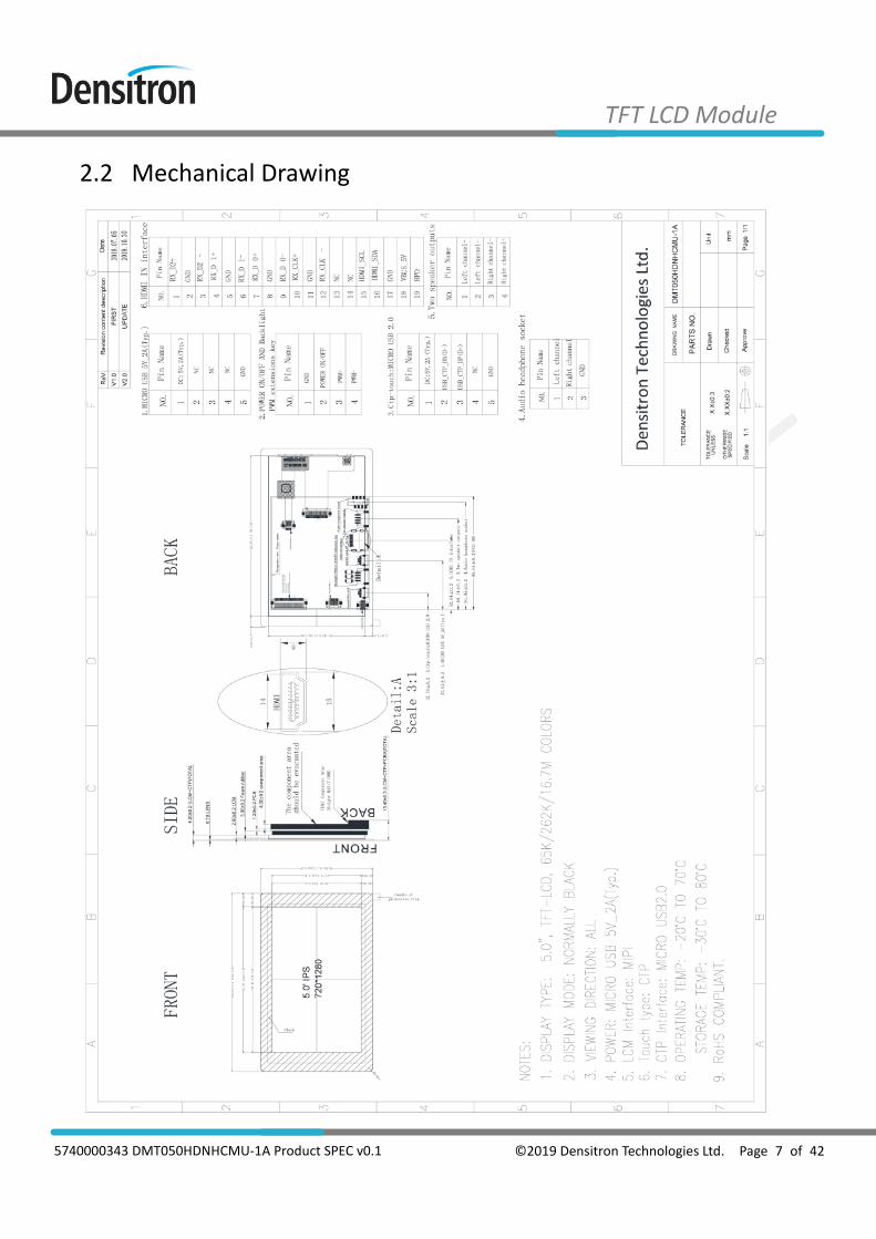
2.1 Mechanical Characteristics
Item Characteristic Unit
Display Format 720 x RGB x 1280 Dots
Overall Dimensions 78.56 (W) x 135.65 (H) x 4.2 (D) mm
Active Area 62.10 (W) x 110.40 (H) mm
Dot Pitch 0.08625 (W) x 0.08625 (H) mm
Weight 98 g
IC Controller/Driver ILI9881C
©2019 Densitron Technologies Ltd. Page 7 of 42 5740000343 DMT050HDNHCMU-1A Product SPEC v0.1
TFT LCD Module
2.2 Mechanical Drawing
©2019 Densitron Technologies Ltd. Page 8 of 42 5740000343 DMT050HDNHCMU-1A Product SPEC v0.1
TFT LCD Module
Electrical Specification
3.1 Absolute Maximum Ratings
Item Symbol Min Max Unit Note
Power Supply Voltage (Analog) VDD-GND -0.3 6.0 V -
VDDp.GND -0.3 6.0 V -
Input Signal Voltage (LED) V(LED) -0.3 6.0 V LED_EN
Input Signal Voltage (PWR) V(PWR) -0.3 5.5 V DCDC EN
Operating Temperature TOP -20 +70 °C 2, 3
Storage Temperature TST -30 +80 °C 2, 3
Note 1: When this module is used beyond the above absolute maximum ratings, permanent breakage of the module
may occur. For normal operations, it is desirable to use this module under the conditions according to Section
3.2 “Electrical Characteristics”, to avoid malfunctioning.
Note 2: Background colour changes slightly depending on ambient temperature. This phenomenon is reversible.
Note 3: Please refer to item of RELIABILITY.
3.2 Electrical Characteristics
Item Symbol Condition Min Typ Max Unit Note
Digital Supply Voltage VCC - 2.5 3.3 6.0 V -
Digital interface supple Voltage IOVCC - 1.65 1.8 3.3 V -
Normal mode Current consumption IDD - -- 40 -- mA -
Level Input Voltage VIH - 0.7*IOVDD - IOVDD V -
VIL - -0.3 - 0.3*IOVDD V -
Level output voltage VOH - 0.8*IOVCC - IOVCC V -

©2019 Densitron Technologies Ltd. Page 9 of 42 5740000343 DMT050HDNHCMU-1A Product SPEC v0.1
TFT LCD Module
3.3 Interface Pin Assignment
MICRO USB 5V_2A(Typ.) PIN Definition & Signal Connector
No. Symbol I/O Function
1 DC:5V,2A(Typ.) P Supply voltage(5.0V,2A Typ.).
2 NC - No Connection.
3 NC - No Connection.
4 NC - No Connection.
5 GND P Ground.
Note: Mirco-USB Connector Dimension:

©2019 Densitron Technologies Ltd. Page 10 of 42 5740000343 DMT050HDNHCMU-1A Product SPEC v0.1
TFT LCD Module
POWER ON/OFF AND Backlight PWM extensions key PIN Definition &
Signal Connector
No. Symbol I/O Function
1 GND - Ground
2 POWER ON/OFF - ON/OFF KEY
3 PWM+ - The backlight brightness of each button is increased by one level until the
maximum brightness reaches (9 level).
4 PWM- - The backlight brightness of each button is reduced by one level until the
lowest brightness reaches (level 9).

©2019 Densitron Technologies Ltd. Page 11 of 42 5740000343 DMT050HDNHCMU-1A Product SPEC v0.1
TFT LCD Module
CTP: MICRO USB PIN Definition & Signal Connector
No. Symbol I/O Function
1 DC:5V,2A(Typ.) P Supply voltage (5.0V,2A Typ.).
2 USB_CTP_DN(D-) I/O USB data negative analog input.
3 USB_CTP_DP(D+) I/O USB data positive analog input.
4 NC I No Connection.
5 GND P Ground.
Note: Mirco-USB Connector Dimension:

©2019 Densitron Technologies Ltd. Page 12 of 42 5740000343 DMT050HDNHCMU-1A Product SPEC v0.1
TFT LCD Module
Audio headphone socket PIN Define & Input Signal Connector
NO. SYMBOL I/O DISCRIPTION
1 Left channel - Audio output left channel
2 Right channel - Audio output right channel
3 GND - Ground
4 GND - Ground

©2019 Densitron Technologies Ltd. Page 13 of 42 5740000343 DMT050HDNHCMU-1A Product SPEC v0.1
TFT LCD Module
Two speaker outputs PIN Define & Input Signal Connector
NO. SYMBOL I/O DISCRIPTION
1 Left channel+ - Audio output left channel
2 Left channel- -
3 Right channel- - Audio output right channel
4 Right channel+ -

©2019 Densitron Technologies Ltd. Page 14 of 42 5740000343 DMT050HDNHCMU-1A Product SPEC v0.1
TFT LCD Module
HDMI PIN Definition & Signal Connector
NO. SYMBOL I/O DISCRIPTION
1 RX_D2+ I HDMI Receiver channel 2 positive analog input.
2 GND P Ground.
3 RX_D2- I HDMI Receiver channel 2 negative analog input.
4 RX_D1+ I HDMI Receiver channel 1 positive analog input.
5 GND P Ground.
6 RX_D1- I HDMI Receiver channel 1 negative analog input.
7 RX_D0+ I HDMI Receiver channel 0 positive analog input.
8 GND P Ground.
9 RX_D0- I HDMI Receiver channel 0 negative analog input.
10 RX_CLK+ I HDMI Receiver clock positive analog input.
11 GND P Ground.
12 RX_CLK- I HDMI Receiver clock negative analog input.
13 NC - No connect
14 NC - No connect
15 HDMI_SCL I/O HDMI Receiver DDC data channel.
16 HDMI_SDA I HDMI Receiver DDC clock channel.
17 GND P Ground.
18 HDMI_5V P HDMI Supply voltage (5.0V).
19 HPD O HDMI Receiver hot plug detect output
Note: HDMI Connector Dimension

©2019 Densitron Technologies Ltd. Page 15 of 42 5740000343 DMT050HDNHCMU-1A Product SPEC v0.1
TFT LCD Module
3.4 Operating Instructions:
- This product supports the following operating systems: Windows 7/8/10, Raspberry Pi, Ubuntu, Andriod.
- Connect the HDMI cable to Windows 7/8/10 or Raspberry Pi or Ubuntu or Andriod.
- Connect the CTP to micro USB.
- Connect the micro USB DC POWER.
3.5 Block Diagram

©2019 Densitron Technologies Ltd. Page 16 of 42 5740000343 DMT050HDNHCMU-1A Product SPEC v0.1
TFT LCD Module
3.6 Timing Characteristics
Please refer to ILITEK IC ILI9881C datasheet for more information.
High Speed Mode – Clock Channel Timing
DSI Clock Channel Timing
DSI Clock Channel Timing Table
Parameter Symbol Signal Min Max Unit
Double UI instantaneous 2 x UIINST CLKP/N 4 25 ns
UI instantaneous Half UIINSTA, UIINSTB
(Note 1) CLKP/N
2
(Note 2) 12.5 ns
Note 1: UI = UIINSTA = UIINSTB
Note 2: Define the minimum value of 24 UI per Pixel, see as below as table.
Limited Clock Channel Speed Table
Data type Two Lanes
speed
Three Lanes
speed
Four Lanes
speed
Data Type = 00 1110 (0Eh), RGB 565, 16 UI per Pixel 566 Mbps 433 Mbps 366 Mbps
Data Type = 01 1110 (1Eh), RGB 666, 18 UI per Pixel 637 Mbps 487 Mbps 412 Mbps
Data Type = 10 1110 (2Eh), RGB 666 Loosely, 24 UI per Pixel 850 Mbps 650 Mbps 550 Mbps
Data Type = 11 1110 (3Eh), RGB 888, 24 UI per Pixel 850 Mbps 650 Mbps 550 Mbps

©2019 Densitron Technologies Ltd. Page 17 of 42 5740000343 DMT050HDNHCMU-1A Product SPEC v0.1
TFT LCD Module
High Speed Mode – Data Clock Channel Timing
DSI Data to Clock Channel Timings
DSI Data to Clock Channel Timings Table
Parameter Signal Symbol Min Max
Data to Clock Setup time DnP/N, n=0 and 1
tDS 0.15 x UI -
Clock to Data Hold Time tDH 0.15 x UI -

©2019 Densitron Technologies Ltd. Page 18 of 42 5740000343 DMT050HDNHCMU-1A Product SPEC v0.1
TFT LCD Module
High Speed Mode – Rising and Fall Timings
Rising and Falling Timings on Clock and Data Channels
Rise and Fall Timings on Clock and Data Channels Table
Parameter Symbol Condition Min Typ Max
Differential Rise Time for Clock tDRTCLK CLKP/N 150 ps - 0.3UI
(Note)
Differential Rise Time for Data tDRTDATA DnP/N n=0 and 1 150 ps - 0.3UI
(Note)
Differential Fall Time for Clock tDFTCLK CLKP/N 150 ps - 0.3UI
(Note)
Differential Fall Time for Data tDFTDATA DnP/N n=0 and 1 150 ps - 0.3UI
(Note)
Note: The display module has to meet timing requirements, which are defined for the transmitter (MCU) on MIPI D-Phy
standard.

©2019 Densitron Technologies Ltd. Page 19 of 42 5740000343 DMT050HDNHCMU-1A Product SPEC v0.1
TFT LCD Module
Low Speed Mode – Bus Turn Around
Lower Power Mode and its State Periods on the Bus Turnaround (BTA) from the MCU to the Display Module (ILI9881C)
are illustrated for reference purposes below.
BTA from the MCU to the Display Module
Lower Power Mode and its State Periods on the Bus Turnaround (BTA) from the Display Module (ILI9881C) to the MCU
are illustrated for reference purposes below.
BTA from the Display Module to the MCU
Low Power State Period Timings – A Table
Description Signal Symbol Min Max Unit
Length of LP-00, LP-01, LP-10 or LP-11 periods
MCU ➔ Display Module (ILI9881C) D0P/N TLPXM 50 75 ns
Length of LP-00, LP-01, LP-10 or LP-11 periods
Display Module (ILI9881C) ➔ MCU D0P/N TLPXD 50 75 ns
Time-out before the Display Module (ILI9881C) starts driving D0P/N TTA-SURED TLPXD 2 x TLPXD ns
Low Power State Period Timings – B Table
Description Signal Symbol Time Unit
Time to drive LP-00 by Display Module (ILI9881C) D0P/N TTA-GETD 5 x TLPXD ns
Time to drive LP-00 after turnaround request - MCU D0P/N TTA-GOD 4 x TLPXD ns

©2019 Densitron Technologies Ltd. Page 20 of 42 5740000343 DMT050HDNHCMU-1A Product SPEC v0.1
TFT LCD Module
Data Lanes from Low Power Mode to High Speed Mode
Data Lanes - Low Power Mode to High Speed Mode Timings
Data Lanes - Low Power Mode to High Speed Mode Timings Table
Description Signal Symbol Min Max Unit
Length of any Low Power State Period DnP/N,
n = 0 and 1 TLPX 50 - ns
Time to drive LP-00 to prepare for HS
Transmission
DnP/N,
n = 0 and 1 THS-PREPARE 40 + 4 x UI 85 + 6 x UI ns
Time to enable Data Lane Receiver line
termination measured from when Dn crosses
VILMAX
DnP/N,
n = 0 and 1 THS-TERM-EN - 35 + 4 x UI ns

©2019 Densitron Technologies Ltd. Page 21 of 42 5740000343 DMT050HDNHCMU-1A Product SPEC v0.1
TFT LCD Module
Data Lanes from High Power Mode to High Speed Mode
Data Lanes - High Speed Mode to Low Power Mode Timings
Data Lanes - High Speed Mode to Low Power Mode Timings Table
Description Signal Symbol Min Max Unit
Time-Out at Display Module (ILI9881C) to
ignore transition period of EoT
DnP/N,
n = 0 and 1 THS-SKIP 40 55 + 4 x UI ns
Time to driver LP-11 after HS burst DnP/N,
n = 0 and 1 THS-EXIT 100 - ns

©2019 Densitron Technologies Ltd. Page 22 of 42 5740000343 DMT050HDNHCMU-1A Product SPEC v0.1
TFT LCD Module
DSI Clock Burst – High Speed Mode to/from Low Power Mode
Clock Lanes - High Speed Mode to/from Low Power Mode Timings
Clock Lanes - High Speed Mode to/from Low Power Mode Timings Table
Description Signal Symbol Min Max Unit
Time that the MCU shall continue sending HS
clock after the last associated Data Lanes has
transitioned to LP mode
CLKP/N TCLK-POST 60 + 52 x UI - ns
Time to drive HS differential state after last
payload clock bit of a HS transmission burst
CLKP/N TCLK-TRAIL 60 - ns
Time to drive LP-11 after HS burst CLKP/N THS-EXIT 100 - ns
Time to drive LP-00 to prepare for HS
transmission CLKP/N TCLK-PREPARE 38 95 ns
Time-out at Clock Lane to enable HS
termination CLKP/N TCLK-TERM-EN - 38 ns
Minimum lead HS-0 drive period before
starting Clock CLKP/N TCLK-PREPARE + TCLK-ZERO 300 - ns
Time that the HS clock shall be driven prior to
any associated Data Lane beginning the
transition from LP to HS mode
CLKP/N TCLK-PRE 8 x UI - ns

©2019 Densitron Technologies Ltd. Page 23 of 42 5740000343 DMT050HDNHCMU-1A Product SPEC v0.1
TFT LCD Module
Timing for DSI video mode
Parameters Symbols Min. Typ. Max. Units
Vertical sync. active VSA TBD TBD - Line
Vertical Back Porch VBP TBD TBD - Line
Vertical Front Porch VFP TBD TBD - Line
Active lines per frame VACT - 1280 - Line
Horizontal sync. active HSA TBD TBD - Pixel
Horizontal Back Porch HBP TBD TBD - Pixel
Horizontal Front Porch HFP TBD TBD - Pixel
Active pixels per line HACT - 800 - Pixel
Line time tline TBD - bps/lane
Bit rate BRbps 200 Note 5 Line
1 UI=1/Bit rate
HAS(pixel)= (tHSA*lane number ) / (UI* pixel format )
HBP(pixel)= (tHBP*lane number ) / (UI* pixel format )
HFP(pixel)= (tHFP*lane number ) / (UI* pixel format )
Example: BRbps = 457Mbps/lane, 1UI=2.1883ns, Frame rate=60Hz, VACT=1280, VSA=2, VBP=30, VFP=20, HACT=720,
HSA=33, HBP=100, HFP=100, Lanenum=4(lane), Pixel Format=24(bit).

©2019 Densitron Technologies Ltd. Page 24 of 42 5740000343 DMT050HDNHCMU-1A Product SPEC v0.1
TFT LCD Module
Note 1: Lanenum: Date lane of MIPI-DSI.
Note 2: Pixel Format: Please reference to “4.1DSI System Interface”.
Note 3: The formula exists slightly error because of the host-transmission way.
Note 4: The best frame rate setting: 2 data lanes:50~60 Hz / 3 data lanes:50~70 Hz / 4 data lanes:50~70 Hz.
Note 5: Please reference to table of “Limited Clock Channel Speed” in 3.6.1
Reset input timing
Reset Timing
Reset Timing Table
Parameter Signal Symbol Min Max Unit
Reset pulse duration
RESX
tRW 10 - uS
Reset cancel tRT
- 5
(note 1,5) mS
- 120
(note 1,6,7) mS
Note 1: The reset cancel also includes required time for loading ID bytes, VCOM setting and other settings from
EEPROM to registers. This loading is done every time when there is H/W reset cancel time (tRT) within 5 ms
after a rising edge of RESX.
Note 2: Spike due to an electrostatic discharge on RESX line does not cause irregular system reset according to as
below as table.
Reset Descript Table
RESX Pulse Action
Shorter than 5us Reset Rejected
Longer than 10us Reset
Between 5us and 10us Reset starts
©2019 Densitron Technologies Ltd. Page 25 of 42 5740000343 DMT050HDNHCMU-1A Product SPEC v0.1
TFT LCD Module
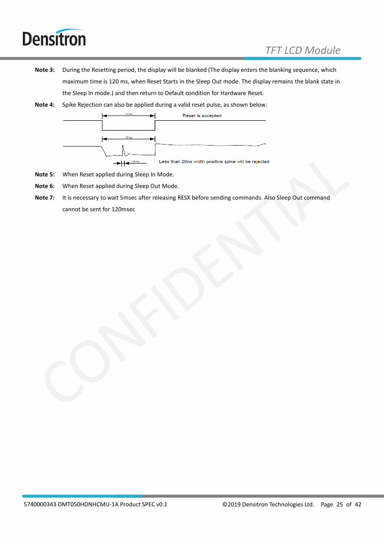
Note 3: During the Resetting period, the display will be blanked (The display enters the blanking sequence, which
maximum time is 120 ms, when Reset Starts in the Sleep Out mode. The display remains the blank state in
the Sleep In mode.) and then return to Default condition for Hardware Reset.
Note 4: Spike Rejection can also be applied during a valid reset pulse, as shown below:
Note 5: When Reset applied during Sleep In Mode.
Note 6: When Reset applied during Sleep Out Mode.
Note 7: It is necessary to wait 5msec after releasing RESX before sending commands. Also Sleep Out command
cannot be sent for 120msec
©2019 Densitron Technologies Ltd. Page 26 of 42 5740000343 DMT050HDNHCMU-1A Product SPEC v0.1
TFT LCD Module
Electrical Specification Touch
4.1 Electrical Characteristics
Absolute Maximum Ratings
Item Symbol Min. Max. Unit Note
Power Supply Voltage VCC 2.66 3.47 V -
Operating temperature TOP -20 +70 ℃ -
Storage temperature TST -30 +80 ℃ -
DC Electrical Characteristics (Ta=25°C)
(Ambient temperature:25℃, AVDD=2.8V, VDDIO=1.8V or VDDIO=AVDD)
Item Symbol Min. Typ. Max. Unit Note
Normal Mode Operating Current - - 8 14.5 mA -
Green Mode Operating Current - - 3.3 - mA -
Sleep Mode Operating Current - 70 - 120 uA -
Doze Mode Operating Current - - 0.78 - mA -
Digital Input Low Voltage VIL -0.3 - 0.25*VDD V -
Digital Input High Voltage VIH 0.75*VDD - VDD+0.3 V -
Digital Output Low Voltage VOL - - 0.15*VDD V -
Digital Output High Voltage VOH 0.85*VDD - - V -
AC Electrical Characteristics (Ta=25°C)
(Ambient temperature:25℃, AVDD=2.8V, VDDIO=1.8V)
Item Symbol Min. Typ. Max. Unit Note
OSC Oscillation Frequency - 59 60 61 MHZ -
I/O Output Rise Time, Low to High - - 14 - ns -
I/O Output Fall Time, High to Low - - 14 - ns -

©2019 Densitron Technologies Ltd. Page 27 of 42 5740000343 DMT050HDNHCMU-1A Product SPEC v0.1
TFT LCD Module
Optical Specification
5.1 Optical Characteristics
Characteristics Symbol Conditions Min Typ Max Unit Note
Contrast Ratio CR = 0°
Normal
viewing angle
640 800 - - 2
Response time TR + TF - 30 40 ms 3
Vie
win
g A
ngl
e Left x-
CR>10
- 80 -
deg 1 Right x+ - 80 -
Up Y+ - 80 -
Down Y- - 80 -
Co
lou
r C
hro
mat
icit
y
Red Rx
= 0°
Normal
viewing angle
0.5639 0.6039 0.6439
- CF
glass
Ry 0.3143 0.3543 0.3943
Green Gx 0.324 0.364 0.404
Gy 0.5494 0.5894 0.6294
Blue Bx 0.1107 0.1507 0.1907
By 0.0639 0.1039 0.1439
White Wx 0.293 0.333 0.373
Wy 0.330 0.370 0.410
Luminance Lv IF = 40mA 380 420 - cd/m2 4
Uniformity Avg - 80 - - % 4
Note Item Test method
1 Definition of Viewing
Angle (x, y)
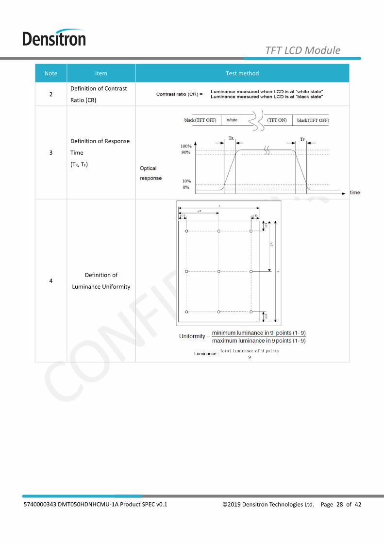
©2019 Densitron Technologies Ltd. Page 28 of 42 5740000343 DMT050HDNHCMU-1A Product SPEC v0.1
TFT LCD Module
Note Item Test method
2 Definition of Contrast
Ratio (CR)
3
Definition of Response
Time
(TR, TF)
4 Definition of
Luminance Uniformity

©2019 Densitron Technologies Ltd. Page 29 of 42 5740000343 DMT050HDNHCMU-1A Product SPEC v0.1
TFT LCD Module
LED Backlight Specification
6.1 LED Backlight Characteristics
Item Symbol Condition Min Typ Max Unit Note
Forward Current IF - 30 40 - mA -
Forward Voltage VF - - 19.2 - V -
LED Life Time Hr - - 50000 - Hour 1, 2
Note 1: LED life time (Hr) can be defined as the time in which it continues to operate under the condition:
Ta=25±3℃, typical IL (IF) value indicated in the above table until the brightness becomes less than 50%.
Note 2: The “LED life time” is defined as the module brightness decreases to 50% original brightness
at Ta=25℃ and IL=40mA. The LED lifetime could be decreased if operating IL is larger than 40mA. The
constant current driving method is suggested.
6.2 INTERNAL CIRCUIT DIAGRAM
©2019 Densitron Technologies Ltd. Page 30 of 42 5740000343 DMT050HDNHCMU-1A Product SPEC v0.1
TFT LCD Module
Packaging TBD

©2019 Densitron Technologies Ltd. Page 31 of 42 5740000343 DMT050HDNHCMU-1A Product SPEC v0.1
TFT LCD Module
Quality Assurance Specification
8.1 Conformity
The performance, function and reliability of the shipped products conform to the Product Specification.
8.2 Environment Required
Customer’s test & measurement are required to be conducted under the following conditions:
Temperature: 25 ± 5C
Humidity: 65% ± 10% RH
Viewing Angle: Normal Viewing Angle
Illumination: Single fluorescent lamp (300 to 700 Lux)
Viewing distance: 30 - 50cm
Finger glove (or finger cover) must be worn by the inspector.
Inspection table or jig must be anti-electrostatic.
8.3 Delivery Assurance
Delivery Inspection Standards
Class II, Normal Inspection, MIL-STD-105E

©2019 Densitron Technologies Ltd. Page 32 of 42 5740000343 DMT050HDNHCMU-1A Product SPEC v0.1
TFT LCD Module
Zone Definition
Zone A: Effective Viewing Area (Character or Digit can be seen)
Zone B: Viewing Area except Zone A
Zone C: Outside (Zone A + Zone B) Area which cannot be seen after assembly by customer.
Zone D: IC Bonding Area
Note: Generally, visual defects in Zone C can be ignored when it doesn’t affect product function or appearance after
assembly by customer

©2019 Densitron Technologies Ltd. Page 33 of 42 5740000343 DMT050HDNHCMU-1A Product SPEC v0.1
TFT LCD Module
Criteria & Acceptable Quality Level
LCD: Liquid Crystal Display, TP: Touch Panel, LCM: Liquid Crystal Module
Partition AQL Definition
Major 0.65 Defects in Pattern Check (Display On)
Minor 1.5 Defects in Cosmetic Check (Display Off)
No. Items Criteria Classification of defects
1 Functional defects
1) No display, open or miss line
2) Display abnormally
3) Backlight no lighting, abnormal lighting.
4) TP no function Major
2 Missing Missing component
3 Outline dimension Overall outline dimension beyond the drawing is not
allowed
4 Color tone Color unevenness, refer to limited sample
Minor
5 Spot Line defect Light dot, Dim spot, Polarizer Bubble; Polarizer
accidented spot.
6 Soldering Appearance Good soldering, Peeling off is not
allowed.
7 LCD/Polarizer/TP Black/White spot/line, scratch, crack, etc.

©2019 Densitron Technologies Ltd. Page 34 of 42 5740000343 DMT050HDNHCMU-1A Product SPEC v0.1
TFT LCD Module
Criteria & Classification
Units: mm
Class Item Criteria
Minor Spot Defect
Round type: as per following drawing, = (X+Y)/2
1) Light Dot (LCD/TP/Polarizer black/white spot, light dot, pinhole, dent, stain)
Size\Zone Acceptable Quantity
A B C
≤0.10 Ignore
Ignore 0.10<≤0.25 4 (distance ≧ 10mm)
0.25<≤0.35 3
0.4< 0
2) Dim Spot (LCD/TP/Polarizer dim dot, light leakage, dark spot)
Size\Zone Acceptable Quantity
A B C
≤0.10 Ignore
Ignore 0.10<≤0.25 4 (distance ≧ 10mm)
0.25<≤0.35 3
0.4< 0
3) Polarizer Accidented Spot
Size\Zone Acceptable Quantity
A B C
≤0.2 Ignore
Ignore 0.3<≤0.5 3 (distance ≧ 10mm)
0.5< TBD
4) Pixel Bad Points (light dot, dim dot, colour dot)
Size\Zone Acceptable Quantity
A B C
≤0.15 Ignore
Ignore 0.2<≤0.3 2 (distance ≧ 10mm)
0.4< TBD
X
Y

©2019 Densitron Technologies Ltd. Page 35 of 42 5740000343 DMT050HDNHCMU-1A Product SPEC v0.1
TFT LCD Module
Class Item Criteria
5) Polarizer Bubble
Size\Zone Acceptable Quantity
A B C
≤0.20 Ignore
Ignore 0.3<≤0.4 4 (distance ≧ 10mm)
0.4<≤0.5 3
0.5< TBD
Minor
Line Defect
(LCD/TP/
Polarizer
backlight
black/white line,
scratch, stain)
Line type: as per following drawing
Width Length Acceptable quantity
A B C
W≤0.05 Ignore Ignore
Ignore 0.05<W≤0.06 L ≤ 4.0 N ≤ 3
0.07<W≤0.08 L ≤ 3.0 N ≤ 2
0.08<W Define as spot defect
Minor LCD
Crack/Broken
Symbols:
X: Length, Y: Width, Z: Height, L: Length of ITO, T: Height of LCD
1) The edge of LCD broken: X≦3.0mm; Y<Inner border line of the seal; Z≦T
2) LCD corner broken: X≦3.0mm; Y≦L; Z≦T
L
W
©2019 Densitron Technologies Ltd. Page 36 of 42 5740000343 DMT050HDNHCMU-1A Product SPEC v0.1
TFT LCD Module
Class Item Criteria
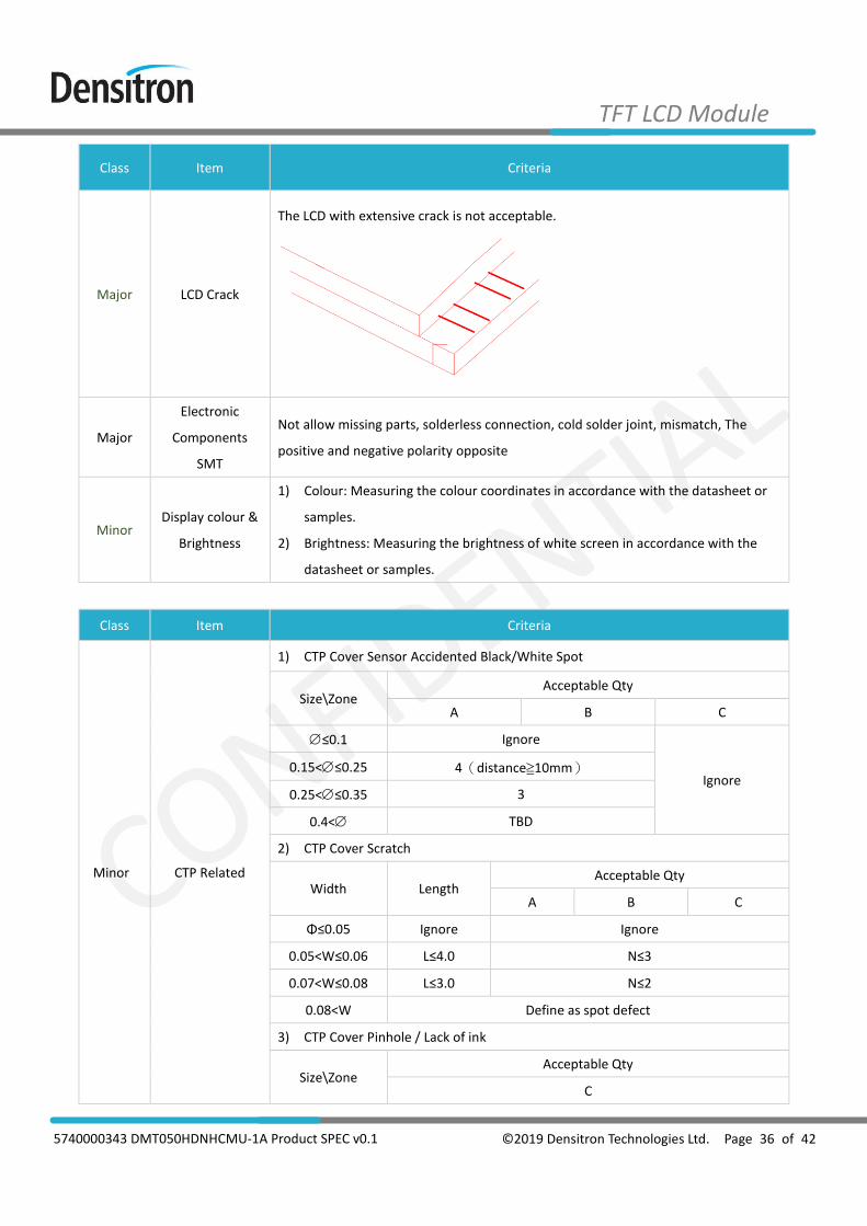
Major LCD Crack
The LCD with extensive crack is not acceptable.
Major
Electronic
Components
SMT
Not allow missing parts, solderless connection, cold solder joint, mismatch, The
positive and negative polarity opposite
Minor Display colour &
Brightness
1) Colour: Measuring the colour coordinates in accordance with the datasheet or
samples.
2) Brightness: Measuring the brightness of white screen in accordance with the
datasheet or samples.
Class Item Criteria
Minor CTP Related
1) CTP Cover Sensor Accidented Black/White Spot
Size\Zone Acceptable Qty
A B C
≤0.1 Ignore
Ignore 0.15<≤0.25 4(distance≧10mm)
0.25<≤0.35 3
0.4< TBD
2) CTP Cover Scratch
Width Length Acceptable Qty
A B C
Φ≤0.05 Ignore Ignore
0.05<W≤0.06 L≤4.0 N≤3
0.07<W≤0.08 L≤3.0 N≤2
0.08<W Define as spot defect
3) CTP Cover Pinhole / Lack of ink
Size\Zone Acceptable Qty
C

©2019 Densitron Technologies Ltd. Page 37 of 42 5740000343 DMT050HDNHCMU-1A Product SPEC v0.1
TFT LCD Module
Class Item Criteria
≤0.2 Ignore
0.2<≤0.3 4 (distance ≧ 10mm)
0.3<≤0.4 3
0.4< 0
4) CTP Bonding Bubble / Accidented Spot
Size\Zone Acceptable Qty
A B
≤0.1 Ignore
0.15<≤0.2 3 (distance≧10mm)
0.2<≤0.25 2
0.25< 0
Assembly Deflection: beyond the edge of backlight ≤0.2mm
Minor CTP Related
TP cover broken X: length, Y: width, Z: height
X≤0.5mm; Y≤0.5mm; Z<Cover thickness
*Circuitry broken is not allowed.
TP cover broken X: length, Y: width, Z: height
X≤0.3mm; Y≤0.3mm; Z<LCD thickness
*Circuitry broken is not allowed.
Criteria (functional items)
No. Item Criteria
1 No display
Not allowed
2 Missing segment
3 Short
4 Backlight no lighting
5 TP no function

©2019 Densitron Technologies Ltd. Page 38 of 42 5740000343 DMT050HDNHCMU-1A Product SPEC v0.1
TFT LCD Module
8.4 Dealing with Customer Complaints
Non-conforming Analysis
Purchaser should supply Densitron with detailed data of non-conforming sample.
After accepting it, Densitron should complete the analysis in two weeks from receiving the sample.
If the analysis cannot be completed on time, Densitron must inform the purchaser.
Handling of Non-conforming Displays
If any non-conforming displays are found during customer acceptance inspection which Densitron is clearly responsible
for, return them to Densitron.
Both Densitron and customer should analyse the reason and discuss the handling of non-conforming displays when the
reason is not clear.
Equally, both sides should discuss and come to agreement for issues pertaining to modification of Densitron quality
assurance standard.

©2019 Densitron Technologies Ltd. Page 39 of 42 5740000343 DMT050HDNHCMU-1A Product SPEC v0.1
TFT LCD Module
Reliability Specification
9.1 Reliability Tests
Test Item Test Condition Sample
Size
Test
Result Note
Low Temperature Operation -20°C, 96 hrs 3ea Pass -
High Temperature Storage 80°C, 96 hrs 3ea Pass -
Low Temperature Storage -30°C, 96 hrs 3ea Pass -
Thermal Humidity
Operating Life test 70℃, 90%RH, 96HR 3ea Pass -
Temperature Cycle
ON/OFF test -20℃ ↔ 70℃, ON/OFF, 20CYC 3ea Pass 1
Thermal Shock
Resistance
The sample should be allowed to stand the
following 5 cycles of operation: TSTL for 30 minutes -> normal
temperature for 5 minutes -> TSTH for 30 minutes -> normal
temperature for 5 minutes, as one cycle, then taking it out and
drying it at normal temperature, and allowing it stand for 24 hours
3ea Pass -
ESD test 150pF, 330Ω , ±6KV(Contact)/± 8KV(Air),
5 points/panel, 10 times/point 3ea Pass -
Box Drop Test 1 Corner 3 Edges 6 faces, 66 cm (MEDIUM BOX) 1box Pass -
Note 1: ON Time over 10 seconds, OFF Time under 10 seconds
Inspection Check Standard
After the completion of the described reliability test, the samples are to be left at room temperature for 4 hrs prior to
conducting the inspection check at 23±5 °C, 55±15% RH.

©2019 Densitron Technologies Ltd. Page 40 of 42 5740000343 DMT050HDNHCMU-1A Product SPEC v0.1
TFT LCD Module
Handling Precautions
10.1 Handling Precautions
1) Since the display panel is being made of glass, do not apply mechanical impacts such us dropping from a high
position.
2) If the display panel is broken by some accident and the internal organic substance leaks out, be careful not to
inhale nor lick the organic substance.
3) If the liquid crystal touches your skin or clothes, wash it off immediately using soap and plenty of water
4) If pressure is applied to the display surface or its neighbourhood of the display module, the cell structure may be
damaged and be careful not to apply pressure to these sections.
5) The polarizer covering the surface of the display module is soft and easily scratched. Please be careful when
handling the display module.
6) When the surface of the polarizer of the display module has soil, clean the surface. It takes advantage of by using
following adhesion tape.
a. Scotch Mending Tape No. 810 or an equivalent
b. Never try to breathe upon the soiled surface nor wipe the surface using cloth containing solvent such as ethyl
alcohol, since the surface of the polarizer will become cloudy.
c. Also, pay attention that the following liquid and solvent may spoil the polarizer:
• Water
• Ketone
• Aromatic Solvents
7) Hold the display module very carefully when placing it into the system housing. Do not apply excessive stress or
pressure to display module. And, do not over bend the film with electrode pattern layouts. These stresses will
influence the display performance. Also, secure sufficient rigidity for the outer cases.
8) Do not apply stress to the LSI chips and the surrounding molded sections.
9) Do not disassemble nor modify the display module.
10) Do not apply input signals while the logic power is off.
11) Pay sufficient attention to the working environments when handing display modules to prevent occurrence of
element breakage accidents by static electricity.

©2019 Densitron Technologies Ltd. Page 41 of 42 5740000343 DMT050HDNHCMU-1A Product SPEC v0.1
TFT LCD Module
a. Be sure to make human body grounding when handling display modules.
b. Be sure to ground tools to use or assembly such as soldering irons.
c. To suppress generation of static electricity, avoid carrying out assembly work under dry environments.
d. Protective film is being applied to the surface of the display panel of the display module. Be careful since static
electricity may be generated when exfoliating the protective film.
12) Protection film is being applied to the surface of the display panel and removes the protection film before
assembling it. If the display module has been stored for a long period of time, residue adhesive material of the
protection film may remain on the surface of the display panel after removed of the film. In such case, remove the
residue material by the method introduced in the above Section 5).
13) If electric current is applied when the display module is being dewed or when it is placed under high humidity
environments, the electrodes may be corroded and be careful to avoid the above.
10.2 Storage Precautions
1) When storing display modules, put them in static electricity preventive bags avoiding exposure to direct sun light
nor to lights of fluorescent lamps, etc. and, also, avoiding high temperature and high humidity environments or
low temperature (less than 0°C) environments. (We recommend you to store these modules in the packaged state
when they were shipped from Densitron) At that time, be careful not to let water drops adhere to the packages or
bags nor let dewing occur with them.
2) If electric current is applied when water drops are adhering to the surface of the display module, when the display
module is being dewed or when it is placed under high humidity environments, the electrodes may be corroded
and be careful about the above.
10.3 Designing Precautions
1) The absolute maximum ratings are the ratings which cannot be exceeded for display module, and if these values
are exceeded, panel damage may be happen.
2) To prevent occurrence of malfunctioning by noise, pay attention to satisfy the VIL and VIH specifications and, at
the same time, to make the signal line cable as short as possible.
3) We recommend you to install excess current preventive unit (fuses, etc.) to the power circuit (VDD). (Recommend
value: 0.5A)
4) Pay sufficient attention to avoid occurrence of mutual noise interference with the neighbouring devices.
5) As for EMI, take necessary measures on the equipment side basically.
6) When fastening the display module, fasten the external plastic housing section.
7) If power supply to the display module is forcibly shut down by such errors as taking out the main battery while the
display panel is in operation, we cannot guarantee the quality of this display module.

©2019 Densitron Technologies Ltd. Page 42 of 42 5740000343 DMT050HDNHCMU-1A Product SPEC v0.1
TFT LCD Module
10.4 Operation Precautions
1) It is indispensable to drive the display within the specified voltage limit since excessive voltage shortens its life.
2) Direct current causes an electrochemical reaction with remarkable deterioration of the display quality. Give
careful consideration to prevent direct current during ON/OFF timing and during operation.
3) Response time is extremely delayed at temperatures lower than the operating temperature range while, at high
temperatures, displays become dark. However, this phenomenon is reversible and does not mean a malfunction
or a display that has been permanently damaged.
4) To protect display modules from performance drops by static electricity rapture, etc., do not touch the following
sections whenever possible while handling the display modules.
a. Pins and electrodes
b. Pattern layouts such as the FPC
5) When the driver is being exposed (COG), semiconductor elements change their characteristics when light is
radiated according to the principle of the solar battery. Consequently, if the driver is exposed to light,
malfunctioning may occur.
a. Design the product and installation method so that the driver may be shielded from light in actual usage.
b. Design the product and installation method so that the driver may be shielded from light during the inspection
processes.
6) Although the display module stores the operation state data by the commands and the indication data, when
excessive external noise, etc. enters into the module, the internal status may be changed. It therefore is necessary
to take appropriate measures to suppress noise generation or to protect from influences of noise on the system
design.
7) We recommend you to construct its software to make periodical refreshment of the operation statuses (re-setting
of the commands and re-transference of the display data) to cope with catastrophic noise.
10.5 Other Precautions
1) Request the qualified companies to handle industrial wastes when disposing of the display modules. Or, when
burning them, be sure to observe the environmental and hygienic laws and regulations.