double driver for econopack+© modules scale …3p_en_v3.pdfthe arcal e+3p module enables to drive...
TRANSCRIPT

PRODUCT SHEET PROTECTIONS & ACCESSORIES
FOR POWER ELECTRONICS ASSEMBLIES
ARCAL E+3P EN V3
All information included in this document is Arcel's or its respective authors' property. Therefore, any reproduction, use, adaptation, modification, integration, translation, commercial use, in whole or in part, by any means or any form (electronic, written or verbal) is forbidden, without prior written permission of Arcel or its respective authors.
ARCEL - ZI du Tronchon - 2, rue des Aulnes - 69544 CHAMPAGNE AU MONT D’OR Cedex - France Tél. 33 (0)4 78 35 02 21 - Fax 33 (0)4 78 35 69 54 – www.arcel.fr
1 de 18
ARCAL E+3P
Double Driver for ECONOPACK+© modules "SCALE TECHNOLOGY"
The ARCAL E+3P module enables to drive an inverter or a chopper arm.
All the functionalities needed for the design of power converters are gathered on two electronic
boards which have the same mechanical dimensions as the ECONOPACK+© module.
The control module ARCAL E+3P includes 3 complementary boards:
ARCAL E+ TOP
ARCAL E+ SCREEN
ARCAL E+ BOT
High isolation and dv/dt
immunity
3W / ±15A per output
Short-circuit protection
Detection of supply default
Default signal in positive logic
Compatible CMOS inputs
Adjustable dead times
±15V grid input
‘Active Clamping’ protection
Measure of temperature through CTN

PRODUCT SHEET PROTECTIONS & ACCESSORIES
FOR POWER ELECTRONICS ASSEMBLIES
ARCAL E+3P EN V3
All information included in this document is Arcel's or its respective authors' property. Therefore, any reproduction, use, adaptation, modification, integration, translation, commercial use, in whole or in part, by any means or any form (electronic, written or verbal) is forbidden, without prior written permission of Arcel or its respective authors.
ARCEL - ZI du Tronchon - 2, rue des Aulnes - 69544 CHAMPAGNE AU MONT D’OR Cedex - France Tél. 33 (0)4 78 35 02 21 - Fax 33 (0)4 78 35 69 54 – www.arcel.fr
2 de 18
CONTENTS
1. Maximum Electrical specifications ............................................................................................ 3
2. Electrical Specifications ........................................................................................................... 3
2.1. Supplies ............................................................................................................................ 3
2.2. Input Stage ....................................................................................................................... 4
2.3. Output stage ..................................................................................................................... 4
3. Functional Diagram .................................................................................................................. 5
4. Mechanical specifications ........................................................................................................ 6
5. General Presentation ............................................................................................................... 7
5.1. Main Specifications ........................................................................................................... 7
6. Detailed Technical Description ................................................................................................. 8
6.1. Driver supply ..................................................................................................................... 8
6.2. Operating Modes (K6) ....................................................................................................... 9
6.3. Default Signal ................................................................................................................. 12
6.4. Control grid (Rg) ............................................................................................................. 13
6.5. ‘Active clamping’ protection............................................................................................. 13
6.6. Monitoring of Short circuits (K9, K10, K11, K12) .............................................................. 15
6.7. Measure of temperature .................................................................................................. 16
6.8. Measure of current .......................................................................................................... 17
6.9. Monitoring of Auxiliary Supplies ...................................................................................... 17
7. Standard Configuration .......................................................................................................... 17
8. Notes ..................................................................................................................................... 18

PRODUCT SHEET PROTECTIONS & ACCESSORIES
FOR POWER ELECTRONICS ASSEMBLIES
ARCAL E+3P EN V3
All information included in this document is Arcel's or its respective authors' property. Therefore, any reproduction, use, adaptation, modification, integration, translation, commercial use, in whole or in part, by any means or any form (electronic, written or verbal) is forbidden, without prior written permission of Arcel or its respective authors.
ARCEL - ZI du Tronchon - 2, rue des Aulnes - 69544 CHAMPAGNE AU MONT D’OR Cedex - France Tél. 33 (0)4 78 35 02 21 - Fax 33 (0)4 78 35 69 54 – www.arcel.fr
3 de 18
1. MAXIMUM ELECTRICAL SPECIFICATIONS
Unless otherwise specified all data are given for 25°C.
Symbol Parameter Min. Max. Unit
VDD Power supply voltage (with reference to the exposed conductive part)i
0 16 VDC
VI Control input 0 VDD VDC
IG Peak grid current -15 +15 A PG Average power per outputii 3 W VISO Isolation test voltage (AC / 50Hz /1min) 4000 Veff VOP Permanent operating voltageiii 1200 VDC dv/dt Immunity in dv/dt at V=1000V 100 KV/µs
TA Operating temperature -40 +85 °C TS Storage temperature -40 +90 °C
VOC Max. voltage of default open collector 40 V IOC Max. current of default open collector 10 mA
2. ELECTRICAL SPECIFICATIONS
Unless otherwise specified all data are given for 25°C.
2.1. Supplies
Symbol Parameter Min. Typ. Max. Unit
VDD Rated power supply 14.5 15 15.5 VDC IDD0 Total off-load supply currentiv 90 mA IDC0 Input current of off-load DC/DC converters 30 mA IDD Total current of maximum supply v 531 mA
Efficiency of the DC/DC converter 85 %
VTH0 Trigger threshold of default vi 11.5 V H Hysteresis of supply defaultvi 0.7 V
PRODUCT SHEET PROTECTIONS & ACCESSORIES
FOR POWER ELECTRONICS ASSEMBLIES
ARCAL E+3P EN V3
All information included in this document is Arcel's or its respective authors' property. Therefore, any reproduction, use, adaptation, modification, integration, translation, commercial use, in whole or in part, by any means or any form (electronic, written or verbal) is forbidden, without prior written permission of Arcel or its respective authors.
ARCEL - ZI du Tronchon - 2, rue des Aulnes - 69544 CHAMPAGNE AU MONT D’OR Cedex - France Tél. 33 (0)4 78 35 02 21 - Fax 33 (0)4 78 35 69 54 – www.arcel.fr
4 de 18
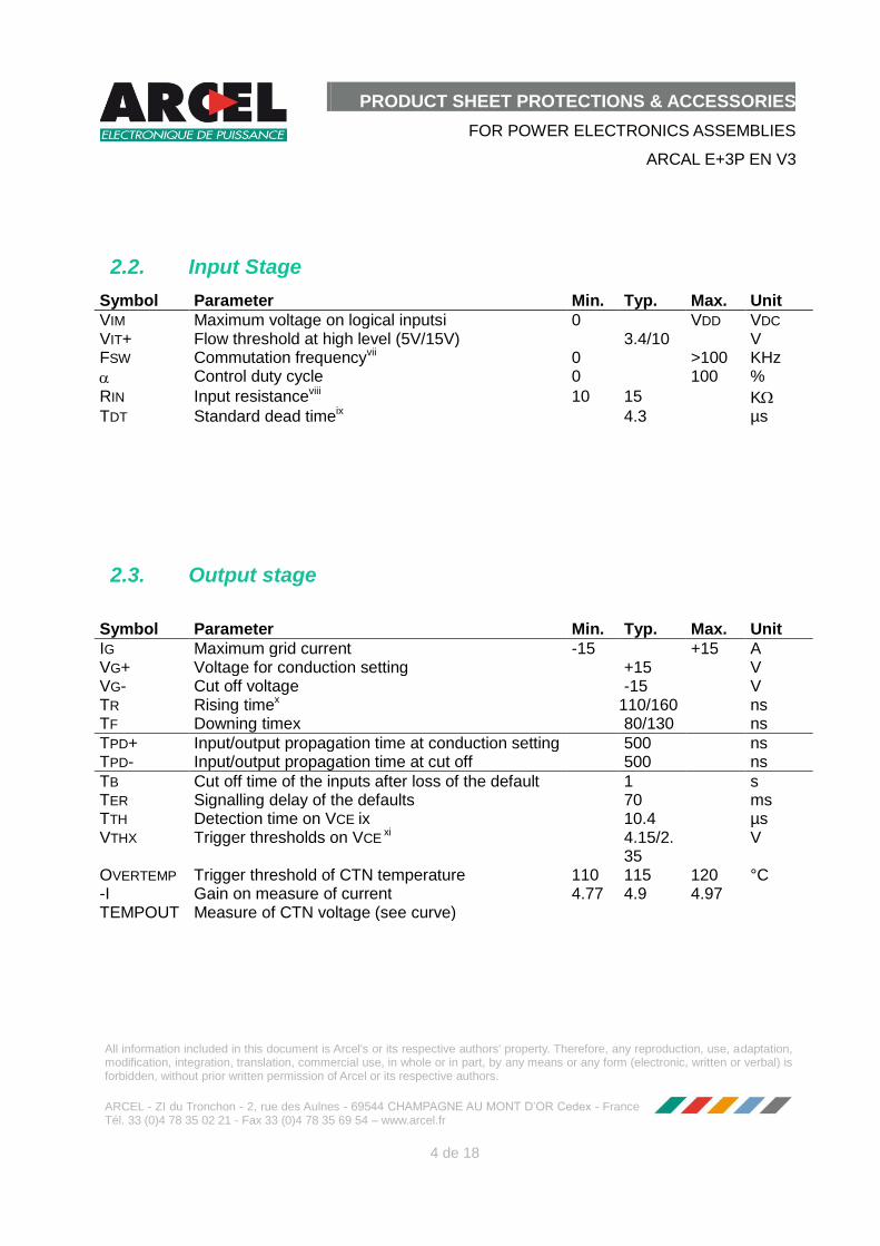
2.2. Input Stage
Symbol Parameter Min. Typ. Max. Unit
VIM Maximum voltage on logical inputsi 0 VDD VDC VIT+ Flow threshold at high level (5V/15V) 3.4/10 V FSW Commutation frequencyvii 0 >100 KHz
Control duty cycle 0 100 %
RIN Input resistanceviii 10 15 K TDT Standard dead timeix 4.3 µs
2.3. Output stage
Symbol Parameter Min. Typ. Max. Unit
IG Maximum grid current -15 +15 A VG+ Voltage for conduction setting +15 V VG- Cut off voltage -15 V TR Rising timex 110/160 ns TF Downing timex 80/130 ns
TPD+ Input/output propagation time at conduction setting 500 ns TPD- Input/output propagation time at cut off 500 ns
TB Cut off time of the inputs after loss of the default 1 s TER Signalling delay of the defaults 70 ms TTH Detection time on VCE ix 10.4 µs VTHX Trigger thresholds on VCE
xi 4.15/2.35
V
OVERTEMP Trigger threshold of CTN temperature 110 115 120 °C -I Gain on measure of current 4.77 4.9 4.97 TEMPOUT Measure of CTN voltage (see curve)

PRODUCT SHEET PROTECTIONS & ACCESSORIES
FOR POWER ELECTRONICS ASSEMBLIES
ARCAL E+3P EN V3
All information included in this document is Arcel's or its respective authors' property. Therefore, any reproduction, use, adaptation, modification, integration, translation, commercial use, in whole or in part, by any means or any form (electronic, written or verbal) is forbidden, without prior written permission of Arcel or its respective authors.
ARCEL - ZI du Tronchon - 2, rue des Aulnes - 69544 CHAMPAGNE AU MONT D’OR Cedex - France Tél. 33 (0)4 78 35 02 21 - Fax 33 (0)4 78 35 69 54 – www.arcel.fr
5 de 18
3. FUNCTIONAL DIAGRAM
GESTION
DEFAUTS / RESET
InA
InB
Shield
JP5 NTC
X3
4
2
Carte inférieureCarte écran Module Econopack
8,9+15 V
VDD
Carte supérieure
AC : Active clamping
VCE SAT : détection du court-circuit
Rgx : résistance de grille
RRC1 CRC1
RRC2 CRC2
51.1K 150 pF
51.1K 150 pF
K1 K2
K3 K4
10,11GND
Temps mort Voie 1Temps mort Voie 2
RESET
Erreur Interne
SELECTIONDU MODEDirect HB
GESTION
DEFAUTS / RESET
Erreur externe
3ERR
K6
1 2 3
TOP TOP TOP
G1
E1
C1
G1
E1
C1
G1
E1
C1
G2
E2
C2
G2
E2
C2
G2
E2
C2
BOT BOT BOT
Viso1
K11Ca
1.5nF
VCE SAT C
Rg2 G
E
AC
51.1K
SORTIE 1
COMMANDE
Viso2
K12Ca
1.5nF
VCE SAT C
Rg2 G
E
AC
51.1K
SORTIE 2
COMMANDE
RTH2
K10
RTH 1
K9
CONTROLE
PRIMAIRE
1
Viso1
Viso2
VDD
Av
-Av
1-15V -15V
12TEMP OUT
Tmax5
14
OVER TEMP
-I
1
2
3
415V
-15V
I
K0
Capteur courant

PRODUCT SHEET PROTECTIONS & ACCESSORIES
FOR POWER ELECTRONICS ASSEMBLIES
ARCAL E+3P EN V3
All information included in this document is Arcel's or its respective authors' property. Therefore, any reproduction, use, adaptation, modification, integration, translation, commercial use, in whole or in part, by any means or any form (electronic, written or verbal) is forbidden, without prior written permission of Arcel or its respective authors.
ARCEL - ZI du Tronchon - 2, rue des Aulnes - 69544 CHAMPAGNE AU MONT D’OR Cedex - France Tél. 33 (0)4 78 35 02 21 - Fax 33 (0)4 78 35 69 54 – www.arcel.fr
6 de 18
4. MECHANICAL SPECIFICATIONS
J4
TOP U
J5
TOP V
J17
TOP W
J18
BOT U
J19
BOT V
J20
BOT WJ21
1 2
13 14
K0
1
2
3
K5123
K6
K2 K1 K4 K3
K7
K9
K8
K10 K0 = Rcurrent
K1 = RRC1
K2 = CRC1/J16
K3 = RRC2
K4 = CRC2/J15
K5 = MODE
TOP/BOT
INA/INB
K6 = MODE
HB (2-3)
DIRECT (1-2)
K7 = Rth1
K8 = Rth2
K9 = CCE1
K10 = CCE2
J15J16
X1
JP
2
1
K0

PRODUCT SHEET PROTECTIONS & ACCESSORIES
FOR POWER ELECTRONICS ASSEMBLIES
ARCAL E+3P EN V3
All information included in this document is Arcel's or its respective authors' property. Therefore, any reproduction, use, adaptation, modification, integration, translation, commercial use, in whole or in part, by any means or any form (electronic, written or verbal) is forbidden, without prior written permission of Arcel or its respective authors.
ARCEL - ZI du Tronchon - 2, rue des Aulnes - 69544 CHAMPAGNE AU MONT D’OR Cedex - France Tél. 33 (0)4 78 35 02 21 - Fax 33 (0)4 78 35 69 54 – www.arcel.fr
7 de 18
1 2
U V W
3 4 5 6
12 11 10 9 8 7
17
15
16
2
TOP
13
14
1
BOT
22
20
21
4
TOP
18
19
3
BOT
27
25
26
6
TOP
23
24
5
BOT
11
12
9
10
7
8
NTC
28
29
Internal layout of the ECONOPACK+© module
5. GENERAL PRESENTATION
The ARCAL E+ driver is based on a SCALE module (Scaleable, Compact, All purpose, Low
cost and Easy to use), the latest generation of drivers which has been acknowledged as "the
best project in power electronics" by ABB Switzerland in 1998.
All the functionalities required for driving power switches (IGBTs) in full safety are gathered
on one single board. Each parameter which could depend on the application can be very easily
configured.
5.1. Main Specifications
The ARCAL E+3P driver enables to drive an ECONOPACK+© module in a half bridge
structure or in an independent way. This driver enables to convert an ECONOPACK+© module
in an independent arm, which can be used in a high power inverter or chopper. This driver is
suitable for IGBTs up to 1800V in its standard version.
The IGBTs are controlled in ±15V.
The IGBTs protection is ensured by monitoring of the VCEsat and of power supplies.

PRODUCT SHEET PROTECTIONS & ACCESSORIES
FOR POWER ELECTRONICS ASSEMBLIES
ARCAL E+3P EN V3
All information included in this document is Arcel's or its respective authors' property. Therefore, any reproduction, use, adaptation, modification, integration, translation, commercial use, in whole or in part, by any means or any form (electronic, written or verbal) is forbidden, without prior written permission of Arcel or its respective authors.
ARCEL - ZI du Tronchon - 2, rue des Aulnes - 69544 CHAMPAGNE AU MONT D’OR Cedex - France Tél. 33 (0)4 78 35 02 21 - Fax 33 (0)4 78 35 69 54 – www.arcel.fr
8 de 18
An ‘Active Clamping’ voltage protection is ensured by monitoring of the collector
voltage.
Only one VDD direct supply of 15V ±0.5V is required. The isolated supplies which are
required on the power side are internally generated.
The logical inputs are equipped with Schmitt triggers.
The logical level of these inputs is selected at 15V (CMOS compatibility).
The dead time value of each channel can be adjusted by the user.
The default signal, which is of type open collector, is activated by the driver (short
circuit or supply default).
The connectors have been selected according to their reliability and in order to
rationalize the implementation of the driver in existing applications.
An intermediary board (ARCAL E+3P SCREEN) enables to realize a chip layout which
will afford a high CEM immunity, as well as an efficient mechanical protection of the
module.
Output of the CTN temperature information and output of open collector at on-state
when the CTN temperature exceeds 115°C.
It is possible to measure the current by means of a power collector.
6. DETAILED TECHNICAL DESCRIPTION
6.1. Driver supply
The ARCAL E+3P driver requires a regulated supply of +15V ±0.5V. The maximum power
used under normal operating conditions is about 8W.
The current used at the input can be calculated according to the following formula:
060.01585.0
WP
AI GT
DD
In which, PGT = total power provided by the driver to the IGBTs.

PRODUCT SHEET PROTECTIONS & ACCESSORIES
FOR POWER ELECTRONICS ASSEMBLIES
ARCAL E+3P EN V3
All information included in this document is Arcel's or its respective authors' property. Therefore, any reproduction, use, adaptation, modification, integration, translation, commercial use, in whole or in part, by any means or any form (electronic, written or verbal) is forbidden, without prior written permission of Arcel or its respective authors.
ARCEL - ZI du Tronchon - 2, rue des Aulnes - 69544 CHAMPAGNE AU MONT D’OR Cedex - France Tél. 33 (0)4 78 35 02 21 - Fax 33 (0)4 78 35 69 54 – www.arcel.fr
9 de 18
INB
INA Output 1
Output 2 ARCALE+3P
Configuration: 1
2
3 K6 J15 J16
Remark:
This product is dedicated to highly impulsive applications and as such there can’t be any
efficient protection of the DC/DC converter against overloads. The board feeder however is
equipped with a fuse which aims to control long-lasting overload risks. These overloads could
possibly damage upstream systems.
6.2. Operating Modes (K6)
The ARCAL E+3P driver can operate according to 2 different modes:
The "DIRECT" mode which enables to drive the two outputs independently.
The "HB" (half-bridge) mode is dedicated to "half-bridge" systems.
Direct Mode
In this mode, the outputs are driven independently
one from the other by the InA and InB inputs. The
different security systems however stop the two
outputs and activate the unique default signal. A
high logical level on one of the InX inputs maps to
the conductive setting of the corresponding IGBT.
The two channels being independent, the driver
won’t generate any dead time. It is therefore
possible to activate the two outputs at the same
time.
The configuration of the driver in DIRECT mode can
be done by connecting the terminals 1 and 2 of K6
and by short-circuiting J15 and J16.
Caution:
A bad operating condition could occur if J15 and J16
are not short-circuited in DIRECT mode!
Outline 1 : Direct Mode
PRODUCT SHEET PROTECTIONS & ACCESSORIES
FOR POWER ELECTRONICS ASSEMBLIES
ARCAL E+3P EN V3
All information included in this document is Arcel's or its respective authors' property. Therefore, any reproduction, use, adaptation, modification, integration, translation, commercial use, in whole or in part, by any means or any form (electronic, written or verbal) is forbidden, without prior written permission of Arcel or its respective authors.
ARCEL - ZI du Tronchon - 2, rue des Aulnes - 69544 CHAMPAGNE AU MONT D’OR Cedex - France Tél. 33 (0)4 78 35 02 21 - Fax 33 (0)4 78 35 69 54 – www.arcel.fr
10 de 18
INB
INA
Output 2
Output 1
ARCAL E+3P
Configuration: 1
2
3 K6 K4 K2
TOP
BOT
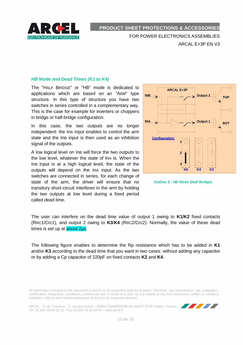
HB Mode and Dead Times (K1 to K4)
The "HALF BRIDGE" or "HB" mode is dedicated to
applications which are based on an "ARM" type
structure. In this type of structure you have two
switches in series controlled in a complementary way.
This is the case for example for inverters or choppers
in bridge or half-bridge configuration.
In this case, the two outputs are no longer
independent: the InA input enables to control the arm
state and the InB input is then used as an inhibition
signal of the outputs.
A low logical level on InB will force the two outputs to
the low level, whatever the state of InA is. When the
InB input is at a high logical level, the state of the
outputs will depend on the InA input. As the two
switches are connected in series, for each change of
state of the arm, the driver will ensure that no
transitory short-circuit interferes in the arm by holding
the two outputs at low level during a fixed period
called dead time.
The user can interfere on the dead time value of output 1 owing to K1/K2 fixed contacts
(RRC1/Crc1), and output 2 owing to K3/K4 (RRC2/Crc2). Normally, the value of these dead
times is set up at about 2µs.
The following figure enables to determine the Rp resistance which has to be added in K1
and/or K3 according to the dead time that you want in two cases: without adding any capacitor
or by adding a Cp capacitor of 220pF on fixed contacts K2 and K4.
Outline 2 : HB Mode (Half Bridge)

PRODUCT SHEET PROTECTIONS & ACCESSORIES
FOR POWER ELECTRONICS ASSEMBLIES
ARCAL E+3P EN V3
All information included in this document is Arcel's or its respective authors' property. Therefore, any reproduction, use, adaptation, modification, integration, translation, commercial use, in whole or in part, by any means or any form (electronic, written or verbal) is forbidden, without prior written permission of Arcel or its respective authors.
ARCEL - ZI du Tronchon - 2, rue des Aulnes - 69544 CHAMPAGNE AU MONT D’OR Cedex - France Tél. 33 (0)4 78 35 02 21 - Fax 33 (0)4 78 35 69 54 – www.arcel.fr
11 de 18
Outline 3 : Value of dead time according to Rrc and Crc
Caution:
The Rp resistance must in no way be lower than 8K.
Logical Inputs
The InA and InB inputs are equipped with Schmitt triggers whose tilting thresholds are about
1/3 and 2/3 of the selected logical level (CMOS). A high logical level fits with an active input
(positive logic).
The input stage of the driver includes protection diodes against negative voltages or against
voltages higher than VDD. If the voltages exceed these limits, an abnormal temperature rise
0,00
1,00
2,00
3,00
4,00
5,00
6,00
7,00
8,00
9,00
10,00
11,00
1 10 100 1000Rp (k)
Value of dead times (µs)
K2/K4 : Cp=220pF
K2/K4 : Défault
Without Rp : 9.9µs
Without Rp : 4.3µs
6

PRODUCT SHEET PROTECTIONS & ACCESSORIES
FOR POWER ELECTRONICS ASSEMBLIES
ARCAL E+3P EN V3
All information included in this document is Arcel's or its respective authors' property. Therefore, any reproduction, use, adaptation, modification, integration, translation, commercial use, in whole or in part, by any means or any form (electronic, written or verbal) is forbidden, without prior written permission of Arcel or its respective authors.
ARCEL - ZI du Tronchon - 2, rue des Aulnes - 69544 CHAMPAGNE AU MONT D’OR Cedex - France Tél. 33 (0)4 78 35 02 21 - Fax 33 (0)4 78 35 69 54 – www.arcel.fr
12 de 18
and/or over-consumption could occur. Safe practice should be taken in case of use of the
driver with large lengths of cable.
Under normal operating conditions the impedance of these outputs is about 15K.
6.3. Default Signal
The "DEFAULT" output is of type open collector. It can resist to a 40V voltage and drain a 10mA
current. An external draught loss must be provided.
The default signal is active at high level : in case of a default, the output transistor is
stopped (high impedance). This is the standard operating mode as a failure of the control cable
will be interpreted as a default by the upstream control system.
In case of internal error
In case of an internal error, the default will be shown during an interval of about 70ms. The
driver will be automatically restarted and the outputs will stay inactive for a minimum time of
1s. The upstream control system is supposed to stop the control pulses as soon as the default
appears. Should the opposite happen, and after the default signalling delay, low-rate
commutations (about 10µs) can occur on the non-default channel. The default will then be
shown again by a 70ms pulse, etc… until the cause of the default has been found out and has
disappeared or until the control pulses have stopped.
Remark
The management of internal defaults is directly done at each output. Thus the default channel
is immediately stopped for a minimum time of 1s. The information feedback towards the input
however only takes place when there is a change of state of the Inx (or InA in HB mode)
inputs. After the blocking period of pulses the system will only start again on a pulse rise of the
concerned InX (or InA in HB mode) input.
Driver powering up
A default pulse (about 70ms) is automatically generated when powering up the driver in order
to enable the auxiliary supplies to settle.
PRODUCT SHEET PROTECTIONS & ACCESSORIES
FOR POWER ELECTRONICS ASSEMBLIES
ARCAL E+3P EN V3
All information included in this document is Arcel's or its respective authors' property. Therefore, any reproduction, use, adaptation, modification, integration, translation, commercial use, in whole or in part, by any means or any form (electronic, written or verbal) is forbidden, without prior written permission of Arcel or its respective authors.
ARCEL - ZI du Tronchon - 2, rue des Aulnes - 69544 CHAMPAGNE AU MONT D’OR Cedex - France Tél. 33 (0)4 78 35 02 21 - Fax 33 (0)4 78 35 69 54 – www.arcel.fr
13 de 18
6.4. Control grid (Rg)
IGBTs are controlled in ±15V. For each output, the conduction setting and the IGBT fade-out
are controlled by a grid resistor: RG.
Peak current
The peak current provided by the driver depends on the total resistance of the Grid/Emitter
loop. Its value can be estimated according to the following formula:
G
GE
GpR
VVAI
In which, VGE represents the variation of the grid voltage (in this case, 30V or 15V) and
RG the grid resistor.
As the IGp current must not exceed 15A, the theoretical low limit for RGON and RGOFF is 2
(for a control of ±15V) or 1 (for a control of 0/15V).
Average power
The average power, PG, provided by a driver output depends on the gate charge, QG, of the
component which is used, on the variation of the grid voltage, VGE, and on the commutation
frequency, FSW (SI units):
SWGEGG FVQP
This power must in no way exceed 3W.
6.5. ‘Active clamping’ protection
This protection aims to limit the emitter collector overvoltage at the opening of the
semiconductor. This overvoltage is the product of the interfering inductance of the loop by the
di/dt imposed by the component.

PRODUCT SHEET PROTECTIONS & ACCESSORIES
FOR POWER ELECTRONICS ASSEMBLIES
ARCAL E+3P EN V3
All information included in this document is Arcel's or its respective authors' property. Therefore, any reproduction, use, adaptation, modification, integration, translation, commercial use, in whole or in part, by any means or any form (electronic, written or verbal) is forbidden, without prior written permission of Arcel or its respective authors.
ARCEL - ZI du Tronchon - 2, rue des Aulnes - 69544 CHAMPAGNE AU MONT D’OR Cedex - France Tél. 33 (0)4 78 35 02 21 - Fax 33 (0)4 78 35 69 54 – www.arcel.fr
14 de 18
The functional diagram is as follows:
As soon as the Vce voltage exceeds a value determined by the transils, a current is injected in
the base of the IGBT thus generating a short renewal phase and enabling to limit de the
tension at the terminals. This device mustn’t be used at continuous rating (i.e. at each
commutation), as it introduces additional losses which can be damaging for the IGBT.
The two above oscillograms (the first one with the device and the second one without it) show
the influence of the device. You can clearly see the limitation of the overvoltage which results
in a clipping.
In the standard version, the voltage protection is set for a 1200V IGBT module. Upon request it
is possible to get a protection for a different voltage (1700V for example).
Control windows 1
2
R2 RE 1 2
D1
TRANSIL
1 2
D3 DIODE
1
2 Q1
IGBT
1 2
3
Vce
D2
TRANSIL
1 2
R1 RG 1 2

PRODUCT SHEET PROTECTIONS & ACCESSORIES
FOR POWER ELECTRONICS ASSEMBLIES
ARCAL E+3P EN V3
All information included in this document is Arcel's or its respective authors' property. Therefore, any reproduction, use, adaptation, modification, integration, translation, commercial use, in whole or in part, by any means or any form (electronic, written or verbal) is forbidden, without prior written permission of Arcel or its respective authors.
ARCEL - ZI du Tronchon - 2, rue des Aulnes - 69544 CHAMPAGNE AU MONT D’OR Cedex - France Tél. 33 (0)4 78 35 02 21 - Fax 33 (0)4 78 35 69 54 – www.arcel.fr
15 de 18
This device enables to limit the overvoltage at the opening to a value close to 1100 volts
(according to the dispersion of the components and the energy that has to be dissipated, the
clipping voltage varies from 1020 to 1100 volts).
6.6. Monitoring of Short circuits (K9, K10, K11, K12)
The detection of short circuits is done by comparing the VCEsat voltage of the device with a
reference voltage. If this threshold level is exceeded, the concerned channel is stopped and
the default signal is activated.
In order to better fit with the IGBT commutation profile, the reference voltage varies according
to the elapsed time since the conduction setting.
First of all the detection has to be
deactivated during a fixed TCE period.
Once this period is over, the detection
threshold is equal to VTH1 and will
progressively decrease (in about 15µs)
until it reaches the VTH2 value. For
each channel, the Tce and VTH
parameters can be modified by a
resistor on K9 terminal (channel 1)
and/or K10 terminal (channel 2) and/or
a CA capacitor on K11 terminal
(channel 1) and K12 terminal (channel
2).
The following diagram gives you an indication of some values of VCEsat detection in relation to
the RTH resistance in use. The Tce value varies in proportion to the overall value of CA,
whereas VTH1 and VTH2 remain nearly the same. This diagram is given for the default value of
CA, i.e. 1.5nF. The useful data is Vth2 and is indicated with two diodes in series, for the
measure of the collector voltage.
Outline 4 : Profile of the reference voltage VTH
Tce
Operating OK
Détection of short-circuit
V T H 1
V T H 2
V T H
t 15 µs
no détection

PRODUCT SHEET PROTECTIONS & ACCESSORIES
FOR POWER ELECTRONICS ASSEMBLIES
ARCAL E+3P EN V3
All information included in this document is Arcel's or its respective authors' property. Therefore, any reproduction, use, adaptation, modification, integration, translation, commercial use, in whole or in part, by any means or any form (electronic, written or verbal) is forbidden, without prior written permission of Arcel or its respective authors.
ARCEL - ZI du Tronchon - 2, rue des Aulnes - 69544 CHAMPAGNE AU MONT D’OR Cedex - France Tél. 33 (0)4 78 35 02 21 - Fax 33 (0)4 78 35 69 54 – www.arcel.fr
16 de 18
RTH TCE VTH2
défaut 7.6 µs 4.15 V
180 K 6.8 µs 3.25 V
82 K 5.7 µs 3 V
51 K 4.9 µs 2.35 V
Diagram 1 : Choice of RTH for VCEsat detection parameters
6.7. Measure of temperature
A CTN is included in the econopack+ housing. The board includes a linearization of this CTN
in the useful operating area. The temperature information is available on pin 12 of the HE14
connector.
Outline 5 : Voltage on pin 12 according to the CTN temperature
1
2
3
4
5
6
7
8
9
10
25 35 45 55 65 75 85 95 105 115 125 135 145
OU
TP
UT
VO
LT
AG
E (
V)
CTN TEMPERATURE (°C)
TEMP OUT

PRODUCT SHEET PROTECTIONS & ACCESSORIES
FOR POWER ELECTRONICS ASSEMBLIES
ARCAL E+3P EN V3
All information included in this document is Arcel's or its respective authors' property. Therefore, any reproduction, use, adaptation, modification, integration, translation, commercial use, in whole or in part, by any means or any form (electronic, written or verbal) is forbidden, without prior written permission of Arcel or its respective authors.
ARCEL - ZI du Tronchon - 2, rue des Aulnes - 69544 CHAMPAGNE AU MONT D’OR Cedex - France Tél. 33 (0)4 78 35 02 21 - Fax 33 (0)4 78 35 69 54 – www.arcel.fr
17 de 18
When the CTN temperature exceeds a 115°C threshold, the potential on output 5 of the HE14
connector is brought to 0V, through the collector of the output transistor.
6.8. Measure of current
It is possible to connect a current sensor on the JP2 connector. In order to operate it, it is
absolutely necessary to supply the HE14 input connector with a -15V voltage on pin 1. On a
standard basis K0 load resistor is 10 Ohms + 1%. The voltage gain on the output stage is -4.9.
The output voltage on pin 14 will thus be equal to:
V (pin 14) = - I sensor x 10 x 4.9
6.9. Monitoring of Auxiliary Supplies
A monitoring of the supply values is directly realised on each output channel. If one of the two
secondary supplies doesn’t exceed 11.5V, the concerned channel is stopped and the default
signal is activated. As the hysteresis of the detection system is 0.7V, the re-start will only occur
once the voltage has gone up again of about 12.2V.
7. STANDARD CONFIGURATION
The standard configuration is as follows:
HB Mode CC between 2 and 3 of K6
Top/Bot Mode CC between 2 and 3 of K5
Delay of 4.3µs
Beginning of active clipping around 1020V for a 1200V module
K0 = 10 Ohms 1%
In which : CC = Short Circuit 1-2 = link terminals 1 and 2
CO = Open Circuit 2-3 = link terminals 2 and 3

PRODUCT SHEET PROTECTIONS & ACCESSORIES
FOR POWER ELECTRONICS ASSEMBLIES
ARCAL E+3P EN V3
All information included in this document is Arcel's or its respective authors' property. Therefore, any reproduction, use, adaptation, modification, integration, translation, commercial use, in whole or in part, by any means or any form (electronic, written or verbal) is forbidden, without prior written permission of Arcel or its respective authors.
ARCEL - ZI du Tronchon - 2, rue des Aulnes - 69544 CHAMPAGNE AU MONT D’OR Cedex - France Tél. 33 (0)4 78 35 02 21 - Fax 33 (0)4 78 35 69 54 – www.arcel.fr
18 de 18
8. NOTES
Before printing think about environment and costs ! N'imprimez ce document que si nécessaire.
CAUTION : ARCEL reserves the right to modify all its technical documentation without prior notice. These documents have no contractual
value.
i The system is protected by zener and bipolar diodes. Exceeding these values can therefore lead to
over heating and/or over consumption. Safe practice should be taken in case of use with large
lengths of cable.
ii Available power at the output of DC/DC converters.
iii Direct voltage or peak value of the alternating voltage executed in a permanent way between the
secondaries or between the secondaries and the primary. Higher values can be guaranteed owing to
a partial loss of load test (which is not done in standard).
iv This value is given for 25KHz control signals.
v If the output power is exceeded, the DC/DC converter will be in an overload state.
vi This security aims at protecting the semi-conductors. Each secondary voltage is individually
monitored. vii
Within the limit of maximum output power. viii
Under normal operating conditions. ix Can be adjusted by the user.
x First value : with a load made up with a 5.6 resistor in series with a 39nF capacitor.
Second value : with a load made up with a 1.8 resistor in series with a 250nF capacitor.
xi Can be adjusted by the user. The two values fit with the detection threshold at Tce and at continuous
rating (about 15µs later).