
Altera Corporation AN-333 - 1.0
March 2004 - ver 1.0
Developing Peripherals forSOPC Builder
Application Note 333
Introduction The SOPC Builder system development tool provides a powerful platform for composing memory-mapped systems based on processors, peripherals, and memories that may be internal or external to the FPGA. A wide variety of components for use with SOPC Builder are available from Altera and third-party vendors. In addition to these off-the-shelf SOPC Builder-ready components, you may want to create your own custom peripheral and connect it to a system using SOPC Builder. By importing a custom peripheral into SOPC Builder, you can easily connect it to an SOPC Builder-generated system in the same manner as commercially available SOPC Builder components.
This document demonstrates how to develop peripherals and import them to be SOPC Builder-ready components. The document has two sections:
■ A brief overview of SOPC Builder and the Avalon™ interface■ Real-world design examples providing a detailed explanation of
developing and importing user-designed components into SOPC Builder.
About the Example Designs
This document and the associated design files are available from the Altera® SOPC Builder literature web page at www.altera.com/literature/ lit-sop.jsp. Two examples design examples are provided:
■ A pulse width modulator (PWM) design implemented as a simple Avalon slave peripheral
■ A VGA video controller implemented as a streaming Avalon slave peripheral
To use the design example, you should be familiar with:
■ The Quartus® II software and SOPC Builder by Altera – For details, refer to the Quartus II Handbook.
■ The Avalon interface – For details, refer to the Avalon Interface Specification Reference Manual.
■ ModelSim® Altera Edition simulation tool by Mentor Graphics®
1Preliminary

Developing Peripherals for SOPC Builder
The example designs were developed using the Nios development kit available from Altera. You can practice importing the design files into SOPC Builder without owning a Nios development kit. However, in order to regenerate the hardware systems or download the systems to hardware, one of the following kits is required:
■ Nios Development Kit, Cyclone™ Edition■ Nios Development Kit, Stratix™ Edition■ Nios Development Kit, Stratix Professional Edition
Overview SOPC Builder automates the task of connecting the address-based read/write interfaces on hardware modules. By automatically integrating modules into a complete system, SOPC Builder dramatically simplifies your task of integrating logic to create a high-performance system-on-a-programmable-chip (SOPC) design. Using SOPC Builder, you only need to specify the components; SOPC Builder automatically generates the interconnect logic, including address decoding, data-path multiplexing, wait-state generation, interrupt controller, and data-width matching. SOPC Builder also generates simulation projects files, testbenches, and execution scripts for simulation on the ModelSim simulator. For the software engineer, SOPC Builder emits header files and driver routines for use by any processor(s) that access peripherals in the system.
SOPC Builder hardware components are comprised of two fundamental pieces:
■ Hardware design files that describe the component hardware■ A component descriptor file called class.ptf for use by SOPC Builder
The class.ptf file contains a database of information about the component, defining how SOPC Builder should integrate the component into a larger system. The process of converting a user-defined block of logic into an SOPC Builder component is creating a class.ptf file and then populating the file with appropriate information.
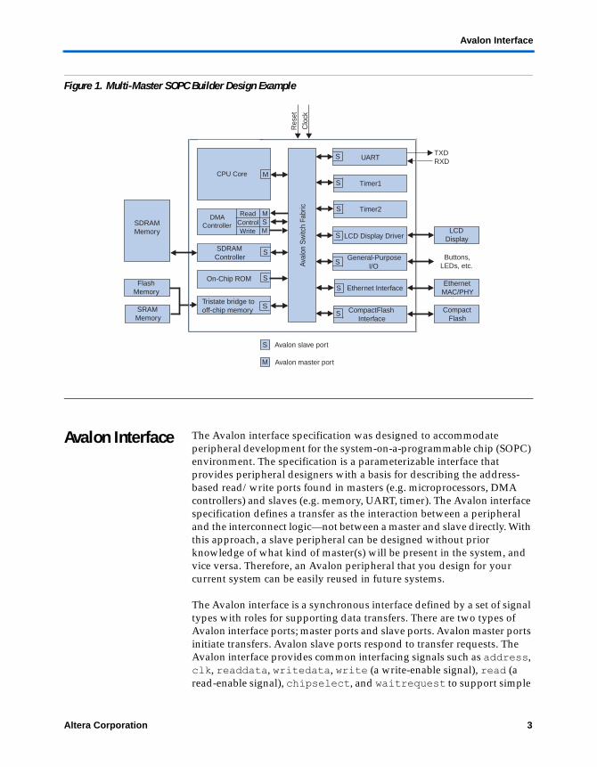
The hardware output of SOPC Builder is a top-level hardware description language (HDL) design file, called the system module. The system module includes the HDL design files that define each of the system components, and the Avalon switch fabric that connects all the components together. SOPC Builder generates the Avalon switch fabric automatically, so designers can focus on designing peripherals rather than creating glue logic to connect the peripheral modules together. Figure 1 on page 3 shows an example of a multi-master system module connecting multiple master and slave peripherals.
2 Altera CorporationPreliminary
Avalon Interface
Figure 1. Multi-Master SOPC Builder Design Example
Avalon Interface The Avalon interface specification was designed to accommodate peripheral development for the system-on-a-programmable chip (SOPC) environment. The specification is a parameterizable interface that provides peripheral designers with a basis for describing the address-based read/write ports found in masters (e.g. microprocessors, DMA controllers) and slaves (e.g. memory, UART, timer). The Avalon interface specification defines a transfer as the interaction between a peripheral and the interconnect logic—not between a master and slave directly. With this approach, a slave peripheral can be designed without prior knowledge of what kind of master(s) will be present in the system, and vice versa. Therefore, an Avalon peripheral that you design for your current system can be easily reused in future systems.
The Avalon interface is a synchronous interface defined by a set of signal types with roles for supporting data transfers. There are two types of Avalon interface ports; master ports and slave ports. Avalon master ports initiate transfers. Avalon slave ports respond to transfer requests. The Avalon interface provides common interfacing signals such as address, clk, readdata, writedata, write (a write-enable signal), read (a read-enable signal), chipselect, and waitrequest to support simple
SDRAMController
Tristate bridge tooff-chip memory
Aval
on S
witc
h Fa
bric
FlashMemory
SRAMMemory
UART
Timer1
Timer2
LCD Display Driver
General-Purpose I/O
Ethernet Interface
CompactFlash Interface
LCD Display
EthernetMAC/PHY
Compact Flash
Buttons, LEDs, etc.
TXDRXD
Clo
ck
Res
et
S
M
Avalon slave port
Avalon master port
S
SDRAMMemory
S
S
S
S
S
S
S
On-Chip ROM S
S
SM
M
ReadControlWrite
DMAController
CPU Core M
Altera Corporation 3Preliminary

Developing Peripherals for SOPC Builder
transfers. Avalon also supports signals for more complex transfers such as latent transfers (also known as posted-read transfers) and streaming transfers.
The Avalon specification allows you to limit the number of interface signals to exactly the signals you need to support the transfer types required for the application. For example, if a peripheral by design can never return data, the Avalon interface does not require any ports related to reading data. This unique feature of the Avalon interface conserves on-chip resources, and makes it particularly well-adapted to malleable SOPC designs.
The Avalon switch fabric defines an interconnect structure that allows any Avalon master port to interact with any Avalon slave port, without prior knowledge of the exact signals present on any peripheral. The Avalon switch fabric supports single-master and multi-master systems. It also allows seamless data transfers between master and slave ports of mismatched data widths.
It is worth repeating that SOPC Builder automatically generates the Avalon switch fabric. As a designer of Avalon peripherals, you only have to design an Avalon interface specifically for your design; you do not have to create the interconnect logic. Your peripherals can employ any subset of the Avalon signal types, regardless of the final system structure.
f For more information on the Avalon interface and Avalon transfers, refer to the Avalon Interface Specification Reference Manual.
SOPC Builder Design Flow
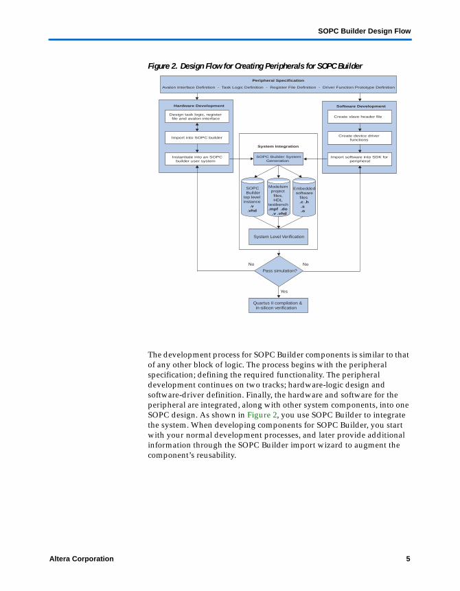
The SOPC Builder system-integration tool facilitates both hardware and software design. The following section provides an overview of the development process for SOPC Builder components. This discussion covers both the hardware and software aspects of component design. By following the procedures described in this document, any Avalon peripheral you create can be integrated in any other SOPC Builder-created system without modifying your peripheral design files. Figure 2 on page 5 shows the design flow for creating peripherals for use with SOPC Builder.
4 Altera CorporationPreliminary
SOPC Builder Design Flow
Figure 2. Design Flow for Creating Peripherals for SOPC Builder
The development process for SOPC Builder components is similar to that of any other block of logic. The process begins with the peripheral specification; defining the required functionality. The peripheral development continues on two tracks; hardware-logic design and software-driver definition. Finally, the hardware and software for the peripheral are integrated, along with other system components, into one SOPC design. As shown in Figure 2, you use SOPC Builder to integrate the system. When developing components for SOPC Builder, you start with your normal development processes, and later provide additional information through the SOPC Builder import wizard to augment the component’s reusability.
Avalon Interface Definition - Task Logic Definition - Register File Definition - Driver Function Prototype Definition
Peripheral Specification
Hardware Development
Design task logic, register file and avalon interface
Import into SOPC builder
Instantiate into an SOPC builder user system
Software Development
Create slave header file
Create device driver functions
Import software into SDK for peripheral
System Integration
SOPC Builder System Generation
System Level Verification
Pass simulation?
No No
Quartus II compilation & in-silicon verification
Yes
Modelsim project files, HDLtestbench.mpf .do .v .vhd
SOPC Buildertop levelinstance .v .vhd
Embedded software files .c .h .s .o
Altera Corporation 5Preliminary

Developing Peripherals for SOPC Builder
Example Design: Avalon Slave Peripheral
This section describes in detail the design process for creating a simple Avalon slave peripheral. For demonstration purposes, we will create a PWM component with an Avalon slave port. The design files are available for you to view, modify, and experiment with. For more information on the design files, see “Using the PWM Component Reference Design” on page 18.
Peripheral Specification
The architecture of a typical Avalon slave peripheral consists of the following functional blocks:
■ Peripheral Task Logic - The peripheral task logic performs the functional operation of the peripheral.
■ Register File - The register file provides a memory element for input to and output from the peripheral task logic.
■ Avalon Interface - The Avalon interface provides a standard address-mapped interface to the register file. The interface provides all the signal types necessary to access the register file and support the transfer types implemented by the task logic.
■ Software Driver Functions - The software driver functions provide the software application interface to the peripheral. The software requirements vary according to the needs of the peripheral. The most common routines initialize the peripheral, read data from the peripheral, or write to the peripheral.
The primarily focus of the peripheral specification is to define the peripheral task logic and the software requirements. With these requirements in place, the register file and Avalon interface are then specified as needed.
A PWM component outputs a square wave with modulated duty-cycle. The basic pulse width waveform is shown in Figure 3.
Figure 3. Basic Pulse-Width Modulation (PWM) Waveform
clk
pwm_out
pwm_duty_cycle = 7
pwm_clock_divide = 10 (+1)
6 Altera CorporationPreliminary

Example Design: Avalon Slave Peripheral
The PWM component was specified and created as follows:
■ The peripheral task logic operates synchronously to a single master clock.
■ To provide a suitable range of PWM periods and duty cycles, 32-bit values are used.
■ A host processor is responsible for setting the PWM period value and duty cycle value. This implies the need for a read/write interface to control logic.
■ Register elements are defined to hold the PWM period value and duty-cycle value.
■ The host processor can halt the PWM output by using an enable control bit.
■ For design reusability, the PWM peripheral must be compatible with any data-width (e.g., 8, 16, 32-bit). Therefore, the interface to the registers supports reading/writing individual bytes.
Hardware Development
As shown in Figure 2 on page 5, hardware development of a SOPC Builder component consists of:
■ Designing the task logic, register file, and Avalon interface■ Importing the design files into SOPC Builder■ Instantiating the component into an SOPC Builder system
As with any logic design process, the development of an SOPC Builder component begins after the specification phase. The coding process is an iterative process involving writing and verifying the HDL logic against the specification. SOPC Builder provides facilities to streamline the development process. Alternately, it is possible to develop and verify peripherals entirely outside of the SOPC Builder development flow.
PWM Task Logic
The PWM task logic consists of an input clock (clk), an output signal (pwm_out), an enable bit, a 32-bit modulo-n counter, and a 32-bit comparator circuit. clk drives the 32-bit modulo-n counter to establish the period of the pwm_out signal. The comparator compares the current value of the modulo-n counter to the duty-cycle value and determines the output of the pwm_out signal. When the current count value is less than or equal to the duty-cycle value, the pwm_out signal drives logic value 0. Otherwise, the pwm_out signal drives logic value 1.The basic task-logic structure is shown in Figure 4 on page 8.
Altera Corporation 7Preliminary

Developing Peripherals for SOPC Builder
Figure 4. Basic PWM Peripheral Structure
Register File
The register file provides access to the enable bit, the modulo-n value and the duty cycle value. For convenience, each of these registers are given read and write access, which means that software can read back the values previously written into the registers. This was done by choice of the designer; we could have equally designed the registers to be write-only, which would conserve on-chip logic resources, yet make it impossible for software to read back the current register values. The designer maps each register to a unique address.
The register file and address mapping is shown in Table 1. Note that to support three registers, two bits of address encoding are necessary. This gives rise to the fourth “reserved” register.
Table 1. Register File & Address Mapping
Register Name Offset Access Description
clock_divide 00 Read /Write The number of clock cycles counted during one cycle of the PWM output.
duty_cycle 01 Read / Write The number of clock cycles in which the PWM output will be low.
enable 10 Read / Write Enables/disables the PWM output. Setting bit 0 to 1 enables the PWM.
Reserved 11 N/A N/A
Up CounterEnableControl Register
Clock Enable
Master Clock
Modulo-n Counter
Modulo-nValue Register
Duty CycleValue Register
=
< =
Reset AvalonSlave Port Signals
PWMOutput
8 Altera CorporationPreliminary

Example Design: Avalon Slave Peripheral
To read or write the registers requires one clock cycle. This affects how wait-states for the Avalon interface are specified as discussed in “Timing Tab” on page 13. Avalon slave ports can be specified to use any number of fixed wait-state cycles, or they can use a variable number of clock cycles. In any case, SOPC Builder will generate the appropriate interconnect logic to assure proper operation between master and slave ports.
Avalon Slave Port
The Avalon slave port is the interface between the switch fabric and the peripheral. The Avalon slave port is a configurable interface and gives designers tremendous flexibility in structuring their peripheral logic. Rather than designing the interface to a strict bus standard with a fixed set of inputs and outputs, the Avalon interface allows designers to include just the inputs and outputs required for the specific Avalon transfer types that the peripheral supports.
SOPC Builder recognizes all of the Avalon interface signal types and their roles. The Avalon switch fabric generated by SOPC Builder matches the transfer capabilities between each master–slave pair.
The Avalon interface for our PWM peripheral requires only a limited set of signals to handle the simple read and write accesses to the registers. Inspection of the Avalon interface specification reveals that support for two basic transfer types are required:
■ Avalon slave read transfer with fixed wait states■ Avalon slave write transfers with fixed wait states
Altera Corporation 9Preliminary

Developing Peripherals for SOPC Builder
Table 2 lists the Avalon signals types required to implement these transfer types, as well as the names of each signal as defined in the HDL design file.
With these signal types and widths, any Avalon master port is capable of transferring data to the PWM component. The PWM peripheral supports the optional byte-enables signals so it can be addressed by master ports with data paths of less then 32-bits. The Avalon interface does not define the naming conventions for signals. As part of the importation process, SOPC Builder maps each signal names to an Avalon signal type. This information is added to the class.ptf component descriptor file for the component.
Verifying the Peripheral
The verification of the peripheral is typically completed in stages. The peripheral task block can be verified using standard behavioral and RTL simulation tools and test benches. The addition of the register file and Avalon signal types of this simple peripheral can often be verified with only minor changes to the test bench. After you import the peripheral into SOPC Builder, you may wish to use Altera’s Nios embedded processor, or another master peripheral, to perform read/write transfers with the peripheral in simulation or in hardware. The Nios processor provides a robust simulation environment that makes verifying custom peripherals a matter of writing C code to initiate transfers to your custom peripheral.
f For more information on simulating Nios processor-based systems, refer to AN 189: Simulating Nios Embedded Processor Designs.
Table 2. PWM Peripheral Port Names & Avalon Signal Types
Signal Name in HDL Avalon Signal Type Bit-Width Direction Notes
clk clk 1 input Primary clock for data transfers and peripheral task logic
write_n write 1 input Write enable signal; active low
write_data writedata 32 input 32-bit write-data value
byte_en_n byteenable 4 input Signals to enable specific byte-lanes.
chip_sel chipselect 1 input Chip-select signal
addr address 2 input 2-bit address; only three encodings are used.
reset_n reset 1 input Reset signal; active low.
read_data readdata 32 output 32-bit read- data value
10 Altera CorporationPreliminary
Example Design: Avalon Slave Peripheral
Importing Design Files into SOPC Builder
Importing a peripheral into SOPC Builder involves the creation of the class.ptf component descriptor file that describes the type and behavior of the ports. SOPC Builder provides an easy–to–use import wizard called Interface to User Logic that automatically generates the class.ptf file for you. The Interface to User Logic wizard provides a graphical user interface (GUI) for importing design files and connecting them to the system. The class.ptf file can be edited with any text editor, but using the Interface to User Logic wizard is recommended.
The Interface to User Logic wizard allows you to:
■ Define the type of interface port on the component, e.g., Avalon master or Avalon slave
■ Import the component design files listing■ Automatically scan design files for input/output signal names■ Map the signal names to Avalon signal types■ Specify timing requirements, such as setup and hold time, or wait
states■ Optionally publish the peripheral to the SOPC Builder pool of
available modules
To see the PWM peripheral integrated into a complete system, you can inspect the provided design files. The remainder of this section discusses the actions taken to integrate the PWM into the over-all design.
Altera Corporation 11Preliminary

Developing Peripherals for SOPC Builder
Ports Tab
Figure 5 shows the Ports tab of the Interface to User Logic wizard used to connect the PWM peripheral.
Figure 5. Ports Tab for the PWM Peripheral
To import the PWM peripheral using the Interface to User Logic wizard, the first step is to select the Bus Interface Type. For the PWM peripheral, we selected the Avalon Register Slave. The Avalon Register Slave selection is used to connect register-mapped peripherals to the system. A register-mapped slave peripheral implies that SOPC Builder should connect the Avalon slave port using native address alignment. In other words, the Avalon switch fabric does not implement dynamic bus sizing for the slave port; one master transfer to the slave port generates exactly one slave transfer. For more information on native address alignment and dynamic bus sizing, refer to the Avalon Interface Specification Reference Manual.
12 Altera CorporationPreliminary
Example Design: Avalon Slave Peripheral
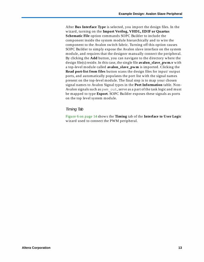
After Bus Interface Type is selected, you import the design files. In the wizard, turning on the Import Verilog, VHDL, EDIF or Quartus Schematic File option commands SOPC Builder to include the component inside the system module hierarchically and to wire the component to the Avalon switch fabric. Turning off this option causes SOPC Builder to simply expose the Avalon slave interface on the system module, and requires that the designer manually connect the peripheral. By clicking the Add button, you can navigate to the directory where the design file(s) reside. In this case, the single file avalon_slave_pwm.v with a top-level module called avalon_slave_pwm is imported. Clicking the Read port-list from files button scans the design files for input/output ports, and automatically populates the port list with the signal names present on the top-level module. The final step is to map your chosen signal names to Avalon Signal types in the Port Information table. Non-Avalon signals such as pwm_out, serve as a part of the task logic and must be mapped to type Export. SOPC Builder exposes these signals as ports on the top level system module.
Timing Tab
Figure 6 on page 14 shows the Timing tab of the Interface to User Logic wizard used to connect the PWM peripheral.
Altera Corporation 13Preliminary

Developing Peripherals for SOPC Builder
Figure 6. Timing Tab for the PWM Peripheral
The Timing tab allows you to set timing parameters that SOPC Builder will use in the generation of the Avalon switch fabric. For the PWM peripheral, the read and write transfers to the registers files were designed as synchronous interfaces that require no setup time, hold time, or wait states. The Read Waveforms and Write Waveforms diagrams change based on the settings to illustrate the Avalon transfers. The Timing tab is disabled for Avalon master peripherals.
At this point, clicking Add to System will add the peripheral to the system. If you need to change parameters later, you can reopen the wizard, modify the values, and then click Add to System to save the changes.
After the component is added to the system, you can make base address and IRQ settings for the component in the SOPC Builder System Contents page. After a master component is added to the system, system generation can take place. SOPC Builder cannot generate systems without at least one master and one slave port. During the generation
14 Altera CorporationPreliminary

Example Design: Avalon Slave Peripheral
process, SOPC Builder copies the HDL for the peripheral to the project directory and generates the appropriate Avalon switch fabric to connect this peripheral to the system.
Publishing a Peripheral as an SOPC Builder Component
The Interface to User Logic function provides you with the option to publish the peripheral so that it appears in the pool of available modules in SOPC Builder. The publishing process locks the parameter values and packages the design files into one directory. This allows you to distribute the component as a single unit that can be reused in other systems. All the settings are locked in, so you do not need to explain to other users how to configure the Avalon interface. After publishing, the parameters cannot be changed. Therefore, you should not publish without first successfully adding the peripheral to a system and testing that the system works.
Publishing the peripheral records information in the class.ptf file for this component, and creates a generation script in a subfolder with the same name of the peripheral. Table 3 shows the directory structure for a published component, using the example PWM component.
Software Development
SOPC Builder allows peripherals designers to associate software files with their peripherals. These files become part of the software development kit (SDK) directory for the overall SOPC Builder-generated system. The associated software files consists of:
■ Header files that declare peripheral-related software structures and constants
■ Peripheral-driver functions to access the peripheral
Table 3. Directory Structure for Published Components
File Name Description
...\user_logic_altera_avalon_pwm Component directory
altera_avalon_pwm.v HDL design file for the peripheral
class.ptf Component descriptor file
mk_user_logic_altera_pwm.pl Generation script SOPC Builder uses at system generation time to integrate the peripheral into the system
Altera Corporation 15Preliminary
Developing Peripherals for SOPC Builder
As with most peripherals used in an embedded system, SOPC Builder components should include a header file (or files) that defines the software view of the hardware. The header file(s) contains register declarations relative to the base address of the peripheral, prototype function declarations, constants, and other configuration information.
The method for providing software files is simple. Each SOPC Builder component directory can contain an SDK directory. This directory reflects the structure of the SDK for a complete SOPC Builder-generated system. At system generation time, SOPC Builder copies files from the component’s SDK directory to the corresponding SDK location for the overall system. In addition, SOPC Builder copies declarations from the component header file(s) into the overall system header file (excalibur.h).
At the present time, you must manually create the SDK directory and it’s subdirectories to add software support for your peripheral.
SDK for the PWM Component
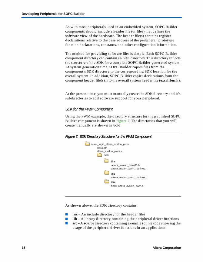
Using the PWM example, the directory structure for the published SOPC Builder component is shown in Figure 7. The directories that you will create manually are shown in bold.
Figure 7. SDK Directory Structure for the PWM Component
As shown above, the SDK directory contains:
■ inc – An include directory for the header files■ lib – A library directory containing the peripheral driver functions■ src – A source directory containing example source code showing the
usage of the peripheral driver functions in an applications
/user_logic_altera_avalon_pwm
/sdk
altera_avalon_pwm.vclass.ptf
altera_avalon_pwm00.haltera_avalon_pwm_routines.h
/inc
/libaltera_avalon_pwm_routines.c
hello_altera_avalon_pwm.c
/src
16 Altera CorporationPreliminary
Example Design: Avalon Slave Peripheral
For our example, the header files in the inc directory contain register map information and function prototypes for the PWM driver functions.
The file in the lib directory contain the low-level peripheral functions to; initialize, enable and disable the PWM output, and change the duty-cycle and period of the PWM output.
The file in the src directory contains an example application demonstrating the PWM driving a LED.
For the PWM peripheral, we provide the following functions:
■ int init_Altera_Avalon_PWM(unsigned int address, unsigned int clock_divider, unsigned int duty_cycle);
■ int enable_Altera_Avalon_PWM(unsigned int address);
■ int disable_Altera_Avalon_PWM(unsigned int address);
■ int change_Altera_Avalon_PWM_Duty_Cycle(unsigned int address, unsigned int duty_cycle);
Each function takes a parameter address, which is the base address of a specific instance of the PWM component.
System Integration
After publishing the PWM component, multiple PWM components can be added to an SOPC Builder system. During system generation, SOPC Builder reads the class.ptf system descriptor files for all components in the system and constructs the Avalon switch fabric to match the interconnect needs of the components. In addition, SOPC Builder builds an SDK directory, as well as ModelSim project files with a testbench for system-level verification.
System-Level Verification
SOPC Builder has integrated support for system-level verification using ModelSim. While, SOPC Builder produces a testbench for system verification, the capability of the simulation environment is dependent on the peripherals included in the system. When a Nios processor is in the system, it is easy to simulate applications software that drives your peripheral.
f See AN189: Simulating Nios Embedded Processor Designs for more information.
Altera Corporation 17Preliminary

Developing Peripherals for SOPC Builder
Using the PWM Component Reference Design
The PWM component reference design files were created using the following software and hardware:
■ Quartus II version 4.0■ Nios Development Kit, version 3.1
This reference design works ”as-is” on the Nios development board, Stratix Edition, Stratix Professional Edition, and Cyclone Edition, and can be used on your own development board with some modification to the design files. The Avalon PWM reference design uses a Nios processor to drive the Avalon PWM component. The PWM output is tied to a LED on the Nios development board. The modulation of the signal driving the LED causes the brightness of the LED to change.
The following steps will not work if you do not have a Nios development kit installed. To download the example design to a Nios development board and run the sample code, follow these steps.
1. Unzip the provided zip file appropriate for your Nios development board, as indicated below:
● Cyclone Edition - Avalon_PWM_1C20● Stratix Edition - Avalon_PWM_1S10 ● Professional Edition - Avalon_PWM_1S40
The zip files contain a Quartus II project directory of a ready-made system containing the PWM peripheral.
2. Use the Quartus II Programmer tool to configure the Altera FPGA with the SOF file in the top-level Quartus II project directory.
3. Open the Nios SDK Shell and type the following to access to the sdk/src directory:
cd <example install directory>/cpu_sdk/src
4. Type the following at the prompt to compile the example software code:
nios-build hello_avalon_slave_pwm.c
5. Type the following at the prompt to download and run the example software code:
nios run hello_avalon_slave_pwm.srec
18 Altera CorporationPreliminary

Example Design: Avalon Slave Port with Streaming Transfer Support
By using the Quartus II software and SOPC Builder, you can also rebuild the project hardware, add additional peripherals, and change the application.
Example Design: Avalon Slave Port with Streaming Transfer Support
This section provides another design example that demonstrates a different configuration of an Avalon slave port. The design for this section is a VGA display controller that uses an Avalon slave port supporting the Avalon streaming transfer mode. The design files are available for you to view, modify, and experiment with. For more information on the design files, see ““Using the Reference Design” on page 26.
Avalon Streaming Transfers
The Avalon interface specification includes advance transfer capabilities that bandwidth performance and/or simplify the design of peripherals. Avalon streaming transfers are defined as an open channel between a master-slave pair which allows successive data transfers using flow-control signals. The streaming transfer mode simplifies the design of systems with a simple master peripheral (e.g. as a DMA controller) that manages bulk data transfers between memories and peripherals. This open channel between the master-slave pair allows data to flow as it becomes available; without requiring the master to continuously poll status registers in the slave peripheral to determine whether it can send or receive data. Streaming transfers maximize throughput between a master-slave pair, while avoiding data overflow or underflow on the slave peripheral.
The Avalon interface specification supports design reuse, even for streaming Avalon peripherals in systems that do not support streaming transfers. For streaming transfers to occur, both the master and the slave ports must support streaming transfers. If either the master or slave port does not support streaming transfers, data transfers simply revert to fundamental Avalon read and write transfers. SOPC Builder automatically generates the appropriate Avalon switch fabric logic for any combination of master and slave ports with and without streaming support.
Peripheral Specification
The architecture of a typical Avalon slave peripheral with streaming support consists of the following functional blocks:
■ Peripheral task logic ■ Register file■ Avalon interface ■ Software driver functions
Altera Corporation 19Preliminary
Developing Peripherals for SOPC Builder
The primarily focus of the peripheral specification is to define the peripheral task logic and the software requirements. With these requirements in place, the register file and Avalon interface are then specified.
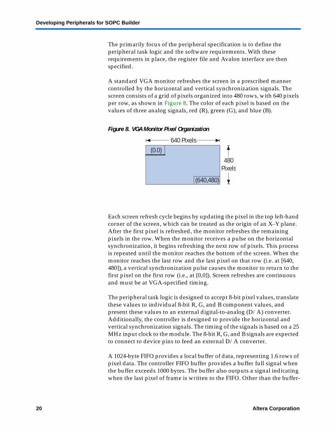
A standard VGA monitor refreshes the screen in a prescribed manner controlled by the horizontal and vertical synchronization signals. The screen consists of a grid of pixels organized into 480 rows, with 640 pixels per row, as shown in Figure 8. The color of each pixel is based on the values of three analog signals, red (R), green (G), and blue (B).
Figure 8. VGA Monitor Pixel Organization
Each screen refresh cycle begins by updating the pixel in the top left-hand corner of the screen, which can be treated as the origin of an X–Y plane. After the first pixel is refreshed, the monitor refreshes the remaining pixels in the row. When the monitor receives a pulse on the horizontal synchronization, it begins refreshing the next row of pixels. This process is repeated until the monitor reaches the bottom of the screen. When the monitor reaches the last row and the last pixel on that row (i.e. at [640, 480]), a vertical synchronization pulse causes the monitor to return to the first pixel on the first row (i.e., at [0,0]). Screen refreshes are continuous and must be at VGA-specified timing.
The peripheral task logic is designed to accept 8-bit pixel values, translate these values to individual 8-bit R, G, and B component values, and present these values to an external digital-to-analog (D/A) converter. Additionally, the controller is designed to provide the horizontal and vertical synchronization signals. The timing of the signals is based on a 25 MHz input clock to the module. The 8-bit R, G, and B signals are expected to connect to device pins to feed an external D/A converter.
A 1024-byte FIFO provides a local buffer of data, representing 1.6 rows of pixel data. The controller FIFO buffer provides a buffer full signal when the buffer exceeds 1000 bytes. The buffer also outputs a signal indicating when the last pixel of frame is written to the FIFO. Other than the buffer-
640 Pixels
(0.0)
480 Pixels
(640,480)
20 Altera CorporationPreliminary
Example Design: Avalon Slave Port with Streaming Transfer Support
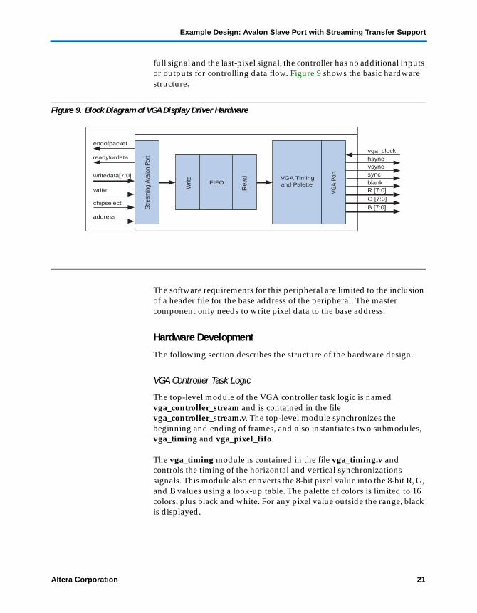
full signal and the last-pixel signal, the controller has no additional inputs or outputs for controlling data flow. Figure 9 shows the basic hardware structure.
Figure 9. Block Diagram of VGA Display Driver Hardware
The software requirements for this peripheral are limited to the inclusion of a header file for the base address of the peripheral. The master component only needs to write pixel data to the base address.
Hardware Development
The following section describes the structure of the hardware design.
VGA Controller Task Logic
The top-level module of the VGA controller task logic is named vga_controller_stream and is contained in the file vga_controller_stream.v. The top-level module synchronizes the beginning and ending of frames, and also instantiates two submodules, vga_timing and vga_pixel_fifo.
The vga_timing module is contained in the file vga_timing.v and controls the timing of the horizontal and vertical synchronizations signals. This module also converts the 8-bit pixel value into the 8-bit R, G, and B values using a look-up table. The palette of colors is limited to 16 colors, plus black and white. For any pixel value outside the range, black is displayed.
Rea
d
Writ
eFIFO
VGA Timingand Palette
VGA
Port
Stre
amin
g Av
alon
Por
tendofpacket
readyfordata
write
chipselect
address
writedata[7:0]
vga_clockhsyncvsyncsyncblankR [7:0]
G [7:0]B [7:0]
Altera Corporation 21Preliminary

Developing Peripherals for SOPC Builder
The vga_pixel_fifo module is contained in the vga_pixel_fifo.v file and is an instantiation of the Altera dual-clock FIFO megafunction, also known as dcfifo. The dcfifo megafunction takes advantage of the dual-port memory structures available in Altera devices to provide independent clock domains for writing and reading the FIFO. The wrusedw[] signal represents the number of words stored in the FIFO, which is used to generate the buffer-full signal specified above.
Register File
The peripheral behaves as if it were a single, 8-bit memory location. The write port to the 8-bit FIFO is mapped to the peripheral’s base address. This peripheral requires only a single write-only address because the 8-bit data stream is input only. There are no configuration options that would require registers. The singular status signal from the peripheral (i.e. buffer-full) is handled by the flow-control signals of the Avalon streaming interface. Therefore, the peripheral behaves as if it were a single 8-bit memory location. Table 4 shows the simple register map.
Avalon Slave Port with Streaming Support
To increase the throughput and minimize the overhead associated with supplying pixel data, we have chosen to use the Avalon streaming- transfer mode. The Avalon signal readyfordata controls the flow of data, and endofpacket signals that the VGA controller has received a complete frame. In this system, the Avalon DMA controller (included with SOPC Builder) performs bulk data transfers from memory to the VGA peripheral. The DMA controller supports streaming transfers and therefore recognizes the readyfordata and endofpacket signals. The handshaking provided by these signals eliminates the need for an intelligent host to check the status of the VGA peripheral prior to sending new data.
Because there is only one location to write to in the VGA controller, address lines are unnecessary. The chipselect signal is sufficient to qualify that an Avalon transfer is occurring. Non-Avalon signals that serve as a part of the task logic (such as the R, G, B, and synchronization outputs), must be mapped to the Export port type. SOPC Builder exposes these signals as ports in the top level system module.
Table 4. Register File & Address Mapping
Register Name Offset Access Descriptionvga_data 0x0 write-only Writing to this register stores the 8-bit value into the
FIFO line-buffer
22 Altera CorporationPreliminary

Example Design: Avalon Slave Port with Streaming Transfer Support
Table 5 shows the complete mapping of the peripheral’s port names to Avalon signal types.
Importing Design Files into SOPC Builder
The following section describes the settings made in the Interface to User Logic wizard.
Ports Tab
We imported the VGA controller design files into SOPC Builder as an Avalon memory slave component using the Interface to User Logic wizard found on the Systems Contents Page of SOPC Builder. The Interface to User Logic wizard shows the result of importing the files. See Figure 10 on page 24. Specifying a peripheral as an Avalon memory slave causes SOPC Builder to build the Avalon switch fabric with addressing appropriate for memory devices. Specifically, SOPC Builder generates dynamic bus-sizing logic. Using dynamic bus sizing allows an Avalon master port to send data wider than the peripheral data width in a single Avalon transfer. The Avalon switch fabric automatically breaks the
Table 5. Avalon Signals for VGA Controller Peripheral
Port Name Avalon Signal Type Bit-Width Direction Description
clock clk 1 input Input clock for writing to the FIFOreset reset 1 input Peripheral resetcs chipselect 1 input Chip selectwrite write 1 input Write-enable signalfifo_data writedata 8 input 8-bit write datafifo_not_full readyfordat
a1 output Streaming transfer signal indicating
that new data is acceptedlastpixel endofpacket 1 output Streaming transfer signal indicating
that the last pixel of a frame was received
vga_clock Export input Input clock for VGA timing and reading data from FIFO
hsync Export 1 output Horizontal synchronization signal (output)
vsync Export 1 output Vertical synchronization signal (output)
sync Export 1 output Logical AND of hsync and vsync (output)
blank Export 1 output Blanking signal during horizontal and vertical synchronization (output)
R Export 8 output Red color (output)G Export 8 output Green color (output)B Export 8 output Blue color (output)
Altera Corporation 23Preliminary
Developing Peripherals for SOPC Builder
transfer into the appropriate number of separate transfers to send all the data to the slave port. For more information on dynamic bus sizing, refer to the Avalon Interface Specification Reference Manual.
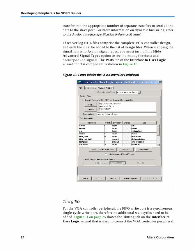
Three verilog HDL files comprise the complete VGA controller design, and each file must be added to the list of design files. When mapping the signal names to Avalon signal types, you must turn off the Hide Advanced Signal Types option to see the readyfordata and endofpacket signals. The Ports tab of the Interface to User Logic wizard for this component is shown in Figure 10.
Figure 10. Ports Tab for the VGA Controller Peripheral
Timing Tab
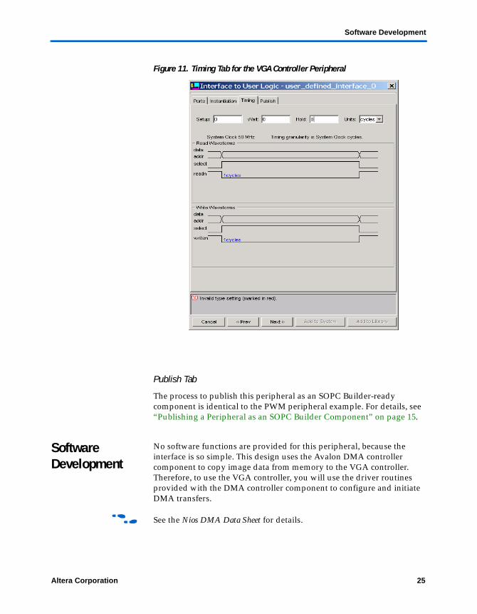
For the VGA controller peripheral, the FIFO write port is a synchronous, single-cycle write port, therefore no additional wait cycles need to be added. Figure 11 on page 25 shows the Timing tab on the Interface to User Logic wizard that is used to connect the VGA controller peripheral.
24 Altera CorporationPreliminary
Software Development
Figure 11. Timing Tab for the VGA Controller Peripheral
Publish Tab
The process to publish this peripheral as an SOPC Builder-ready component is identical to the PWM peripheral example. For details, see “Publishing a Peripheral as an SOPC Builder Component” on page 15.
Software Development
No software functions are provided for this peripheral, because the interface is so simple. This design uses the Avalon DMA controller component to copy image data from memory to the VGA controller. Therefore, to use the VGA controller, you will use the driver routines provided with the DMA controller component to configure and initiate DMA transfers.
f See the Nios DMA Data Sheet for details.
Altera Corporation 25Preliminary
Developing Peripherals for SOPC Builder
Using the Reference Design
The following section describes how to use the VGA reference design.
Overview
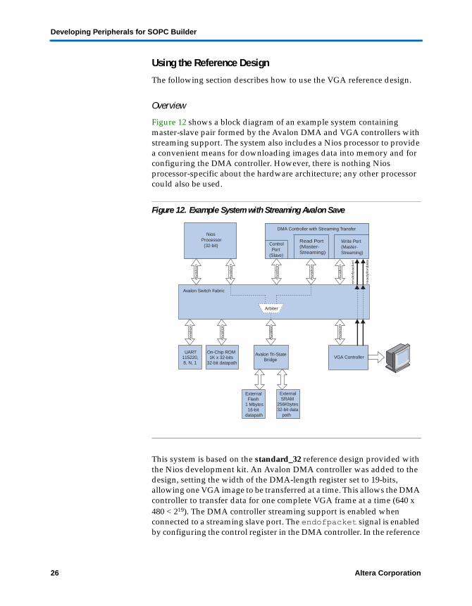
Figure 12 shows a block diagram of an example system containing master-slave pair formed by the Avalon DMA and VGA controllers with streaming support. The system also includes a Nios processor to provide a convenient means for downloading images data into memory and for configuring the DMA controller. However, there is nothing Nios processor-specific about the hardware architecture; any other processor could also be used.
Figure 12. Example System with Streaming Avalon Save
This system is based on the standard_32 reference design provided with the Nios development kit. An Avalon DMA controller was added to the design, setting the width of the DMA-length register set to 19-bits, allowing one VGA image to be transferred at a time. This allows the DMA controller to transfer data for one complete VGA frame at a time (640 x 480 < 219). The DMA controller streaming support is enabled when connected to a streaming slave port. The endofpacket signal is enabled by configuring the control register in the DMA controller. In the reference
Nios Processor (32-bit) Control
Port(Slave)
Write Port(Master-Streaming)
DMA Controller with Streaming TransferA
va
lon
Ava
lon
Avalo
n
Avalo
n
Ava
lon
Avalo
n
Avalo
n
Avalon Switch Fabric
Arbiter
Ava
lon
endofp
acket
readyfo
rdata
Avalo
n
UART115220, 8, N, 1
On-Chip ROM 1K x 32-bits32-bit datapath
Avalon Tri-State Bridge
External Flash1 Mbytes 16-bitdatapath
External SRAM256Kbytes32-bit data path
VGA Controller
Read Port(Master-Streaming)
26 Altera CorporationPreliminary

Software Development
design, when the VGA controller asserts its endofpacket signal, the DMA controller generates an interrupt to the processor. Upon IRQ, the Nios processor’s interrupt service routine takes the following actions:
■ Clears the interrupt ■ Updates the pixel data source■ Configures another DMA transfer by setting the DMA controller
registers■ Starts the DMA transfer
Using the Design Files
The VGA controller peripheral has been hardware tested using the Lancelot VGA development kit daughter-board. A standard VGA monitor plugs into the Lancelot daughter-board, which connects to a Nios development board. For this example design, the Lancelot daughter-board connects to J8, J9 and J10 on the Nios development board. Ordering information for the Lancelot VGA development kit is provided on the Altera website (www.altera.com) in the development kits section.
To run the example design on your Nios development board with the Lancelot VGA daughter card follow these steps.
1. Unzip the provided zip file appropriate for your Nios development board, as shown below:
● Cyclone Edition - streaming_slave_1C20● Stratix Edition - streaming_slave_1S10 ● Professional Edition - streaming_slave_1S40
The zip file contains a Quartus II project directory of a ready-made system containing the VGA controller.
2. Use the Quartus II Programmer to configure the Altera FPGA with the SOF file in the top-level Quartus project directory.
3. Open the Nios SDK Shell and change directories by typing the following:
cd <example install directory>/cpu_sdk/src/image
4. Type the following at the prompt to load the 256 color (8-bit) 640x480 picture into SRAM at address 0x810400
nios-run car_256color.srec
Altera Corporation 27Preliminary

Developing Peripherals for SOPC Builder
You can also use the nios-run command to download any Intel-Hex file or srec file containing the contents of your own image. The Lancelot VGA development kit includes a software application for converting a bitmap (.bmp) image to an S-record format.
5. Type the following at the prompt to rebuild the application software at the .../cpu_sdk/src directory:
cd..
nios-build streaming.c
6. Type the following at the prompt to download and run the example software code:
nios-run streaming.srec
Beyond these steps, you can experiment with the design files by adding additional peripherals, rebuilding the SOPC Builder project, rebuilding the Quartus II project, and/or editing and rebuilding the application software.
28 Altera CorporationPreliminary
101 Innovation DriveSan Jose, CA 95134(408) 544-7000www.altera.comApplications Hotline:(800) 800-EPLDLiterature Services:[email protected]
Copyright © 2004 Altera Corporation. All rights reserved. Altera, The Programmable Solutions Company,the stylized Altera logo, specific device designations, and all other words and logos that are identified astrademarks and/or service marks are, unless noted otherwise, the trademarks and service marks of AlteraCorporation in the U.S. and other countries. All other product or service names are the property of their re-spective holders. Altera products are protected under numerous U.S. and foreign patents and pendingapplications, maskwork rights, and copyrights. Altera warrants performance of its semiconductor productsto current specifications in accordance with Altera's standard warranty, but reserves the right to make chang-es to any products and services at any time without notice. Altera assumes no responsibility or liabilityarising out of the application or use of any information, product, or service describedherein except as expressly agreed to in writing by Altera Corporation. Altera customersare advised to obtain the latest version of device specifications before relying on any pub-lished information and before placing orders for products or services.
Printed on recycled paper


