Download - Ebeam Deposition
7/31/2019 Ebeam Deposition
http://slidepdf.com/reader/full/ebeam-deposition 1/16
An Overview: Electron Beam-Physical Vapor Deposition Technology- Present and FutureApplications
Jogender Singh, Farhat Quli, Douglas E. Wolfe, J. T. Schriempf and Jason Singh
The Applied Research Laboratory,
The Pennsylvania State University,
University Park, PA 16804.
Abstract:
Metallic and ceramic coatings including chromium, molybdenum, titanium carbide (TIC),
and yttria partially stabilized zirconia (YSZ) coatings deposited by electron beam-physical vapor
deposition (EB-PVD) will be presented along with their potential applications. Coatings are oftenapplied on a variety of materials to extend the life of components under severe thermal, corrosion,
wear, and oxidation environments. Interest in replacing chromium electroplating has sparked the
use of EB-PVD technology for the repair of navy landing gear due to the high deposition rates of
the EB-PVD process. The surface morphology, microstructure, and texturing of TiC films
produced by reactive ion beam-assisted, EB-PVD will also be discussed for wear resistant
applications in the cutting tool industry. YSZ has also been grown by EB-PVD resulting in a
columnar microstructure for thermal barrier applications (TBC). Significant improvements in thelife of turbine components are obtained over plasma sprayed YSZ due to the quality and
microstructure of EB-PVD coatings. Scanning electron microscopy, X-ray diffraction, and electron
probe microanalysis (EPMA) was used to characterize the films. In summary, this paper gives a
broad overview of the various ceramic-metallic coatings deposited by EB-PVD at the Applied
Research Laboratory, The Pennsylvania State University.
IntroductionElectron beam-physical vapor deposition (EB-PVD) is a derivative of the electron beam melting
technique. [Records reveal the first U.S. patent was issued to M. Von Pirani in EB melting and
refining of materials in March 1907.] Perhaps the most consequential growth phase in EB
technology began in the early 80s and is still in progress. This significant progress was driven by
three factors: (1) much improved vacuum generation technology, (2) significant advances in
computers, and (3) availability of high-quality EB guns. Since then, EB coating technology isconstantly gaining reputation and confidence in a wide range of applications including thermalbarrier ceramic coatings and wear-resistant hard coatings.
The role of coatings is significant in the advancement of technologies for applications in the optics,
auto, and aerospace industries. A high percentage (75%) of aircraft engine components is coated
by metallic or ceramic coatings for the purpose of enhancing performance and reliability. Thus,
there is a continuous effort to engineer surface properties to enhance the life of componentsunder severe environmental conditions where corrosion, high-temperature oxidation, and wear are
concerns. Similarly, multilayered ceramic and metallic films are used in the fabrication of
microelectronic components. Processes to control thin film properties are also extremely importantin the microelectronic industry.
Before proceeding, three questions need to be answered:1. What are coating processes?2. What is the uniqueness of the EB-PVD process?
3. What are ideal applications for EB-PVD coatings?
7/31/2019 Ebeam Deposition
http://slidepdf.com/reader/full/ebeam-deposition 2/16
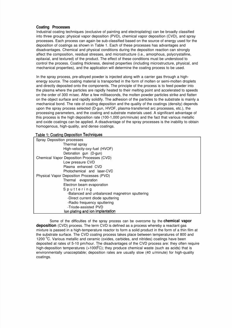
Coating ProcessesIndustrial coating techniques (exclusive of painting and electroplating) can be broadly classified
into three groups: physical vapor deposition (PVD), chemical vapor deposition (CVD), and spray
processes. Each process can again be sub-classified based on the source of energy used for the
deposition of coatings as shown in Table 1. Each of these processes has advantages and
disadvantages. Chemical and physical conditions during the deposition reaction can strongly
affect the composition, residual stresses, and microstructure (i.e., amorphous, polycrystalline,
epitaxial, and textured) of the product. The effect of these conditions must be understood tocontrol the process. Coating thickness, desired properties (including microstructure, physical, and
mechanical properties), and the application will determine the coating process to be used.
In the spray process, pre-alloyed powder is injected along with a carrier gas through a high-
energy source. The coating material is transported in the form of molten or semi-molten droplets
and directly deposited onto the components. The principle of the process is to feed powder into
the plasma where the particles are rapidly heated to their melting point and accelerated to speeds
on the order of 300 m/sec. After a few milliseconds, the molten powder particles strike and flatten
on the object surface and rapidly solidify. The adhesion of the particles to the substrate is mainly a
mechanical bond. The rate of coating deposition and the quality of the coatings (density) depends
upon the spray process selected (D-gun, HVOF, plasma-transferred arc processes, etc.), the
processing parameters, and the coating and substrate materials used. A significant advantage of
this process is the high deposition rate (100-1,000 pm/minute) and the fact that various metallic
and oxide coatings can be applied. A disadvantage of the spray processes is the inability to obtainhomogenous, high-quality, and dense coatings.
Spray Deposition processes
Thermal sprayHigh-velocity-oxy-fuel (HVOF)
Detonation gun (D-gun)
Chemical Vapor Deposition Processes (CVD)Low pressure CVD
Plasma enhanced CVD
Photochemical and laser-CVDPhysical Vapor Deposition Processes (PVD)Thermal evaporation
Electron beam evaporation
S p u t t e r i n g-Balanced and unbalanced magnetron sputtering
-Direct current diode sputtering
-Radio frequency sputtering
-Triode-assisted PVD
Some of the difficulties of the spray process can be overcome by the chemical vapordeposition (CVD) process. The term CVD is defined as a process whereby a reactant gas
mixture is passed in a high-temperature reactor to form a solid product in the form of a thin film atthe substrate surface. The CVD coating process takes place between temperatures of 800 and1200
0C. Various metallic and ceramic (oxides, carbides, and nitrides) coatings have been
deposited at rates of 5-10 pm/hour. The disadvantages of the CVD process are: they often require
high-deposition temperatures (>10000C); they produce chemical waste (such as acids) that is
environmentally unacceptable; deposition rates are usually slow (40 u/minute) for high-quality
coatings.
7/31/2019 Ebeam Deposition
http://slidepdf.com/reader/full/ebeam-deposition 3/16
Some of the shortcomings of the CVD process can be addressed by the physical vapordeposition (PVD) process. The term PVD denotes those vacuum deposition processes where the
coating material is evaporated by various mechanisms (resistance heating, high-energy ionized
gas bombardment, or electron gun) under vacuum, and the vapor phase is transported to the
substrate, forming a coating. PVD is a line-of-sight process in which atoms travel from the source
material to the substrate in a straight path. The PVD coating process takes place between
temperatures of 100-600 C. Sputtering is one of the most versatile PVD processes available for
thin film preparation. Various metallic and ceramic (carbides and nitrides) coatings can be appliedby this process typically at a rate of a few um or less per hour. Unlike the CVD process, PVD
processes are clean and pollution free. The main disadvantages of PVD processes (with
exception of EB-PVD) are the low deposition rates (1-5 pm per hour) and the difficulty in applying
oxide coatings efficiently.
In spite of significant advancements in the various PVD processes (such as cathodic-arc
and DC and RF unbalanced-magnetron sputtering), there are still drawbacks in coating quality.
For example, the cathodic-arc PVD process produces liquid droplets or macro-particles of metals,
1 um to 15 um in size, during the evaporation of the target material. These molten particles can be
entrapped in the growing film, resulting in nonhomogeneity in the microstructure and detrimental
physical properties. In sputtering processes, an applied electric field produces plasma of inert-gasions, which strike the cathode composed of the source material, and ejects atoms from it. Atoms
from the source material are deposited on the surface of the substrate, where they can alsocombine with reactive gases to form ceramic coatings (e.g., TIN, NbN, etc.).
Ion implantation is not a deposition process, but rather a surface modification process inwhich appropriate atoms are embedded in a material through high-energy beams. High-energy
ions are produced in an accelerator and directed on the surface of the substrate. A high-energy
ion implanter (1-10 MeV) is required for deep penetration (-5 pm). Ionized particles enter into the
substrate with kinetic energies four to five orders of magnitude greater than the binding energy of
the solid by a collision mechanism. The principal application of ion implantation has been in theelectronic industries. The disadvantage of the ion implantation process is the limited depth of
penetration into the substrate (< 5um).
Ion plating is a derivative of ion implantation in which the substrate is made the cathodeand the source material is thermally evaporated before being partially ionized and accelerated to
the substrate (cathode). By the proper selection of materials and gas, carbides, nitrides, and
oxides can be deposited. Potential applications of ion plating are in tool industries and certain
aircraft components. Disadvantages of the above mentioned PVD processes can be addressedby the EB-PVD.
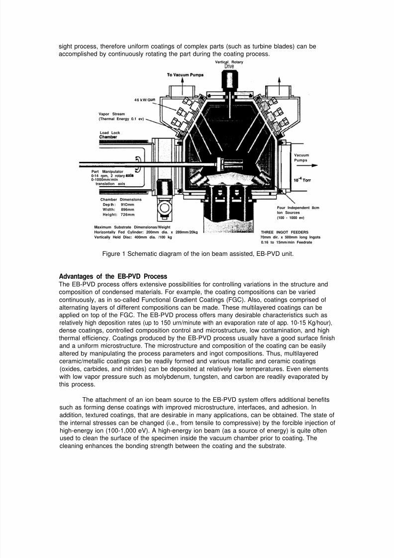
The EB-PVD ProcessThe electron beam-physical vapor deposition (EB-PVD) process has overcome some of thedifficulties associated with the CVD, PVD, and metal spray processes. In the EB-PVD process,
focused high-energy electron beams generated from electron guns are directed to melt and
evaporate ingots, as well as to preheat the substrate inside the vacuum chamber (Figure 1).
Penn State’s industrial pilot Sciaky EB-PVD unit has six electron beam guns, four of which areused to evaporate the coating materials and two of which are used to preheat the substrate to
facilitate coating adhesion. Each gun has a 45-kW capacity. The chamber will accommodate up to
three ingots ranging in size from 49-68 mm in diameter and 450 mm long. The overall dimension
of the production unit is about 1 cubic meter. [The maximum diameter of the substrate (with
vertical rotation) that can be accommodated is about 400 mm; and can be rotated at a speed of
5.5 to 110 rpm with a maximum load of about 100-Kg.] The unit also has a horizontal sample
holder with a three-axis part manipulator: two rotary axes of 0-14 rpm and a 0-4,000 mm/min
translation axis. It can carry samples weighing up to 20 kg. Since, EB-PVD is primarily a line-of-
7/31/2019 Ebeam Deposition
http://slidepdf.com/reader/full/ebeam-deposition 4/16
sight process, therefore uniform coatings of complex parts (such as turbine blades) can beaccomplished by continuously rotating the part during the coating process.
Vertical Rotary
Drive
46 kW/G
Vapor Stream
(Thermal Energy 0.1 ev)
Load Lock
Part Manipulator0-14 rpm, 2 rotary0-1000mm/mln
translatlon axis
Vacuum
Pumps
Chamber Dimenslons
Dep th : 91Omm
Width: 896mm
Height: 726mm
Four Independent 8cm
Ion Sources
(100 - 1000 ev)
Maximum Substrate Dimenslonas/Weight
Horizontally Fed Cylinder: 200mm dia. x 289mm/20kg THREE INGOT FEEDERS
Vertically Held Disc: 400mm dia. /100 kg 70mm dir. x 500mm long Ingots
0.16 to 15mm/min Feedrate
Figure 1 Schematic diagram of the ion beam assisted, EB-PVD unit.
Advantages of the EB-PVD ProcessThe EB-PVD process offers extensive possibilities for controlling variations in the structure and
composition of condensed materials. For example, the coating compositions can be variedcontinuously, as in so-called Functional Gradient Coatings (FGC). Also, coatings comprised of
alternating layers of different compositions can be made. These multilayered coatings can beapplied on top of the FGC. The EB-PVD process offers many desirable characteristics such as
relatively high deposition rates (up to 150 urn/minute with an evaporation rate of app. 10-15 Kg/hour),
dense coatings, controlled composition control and microstructure, low contamination, and high
thermal efficiency. Coatings produced by the EB-PVD process usually have a good surface finish
and a uniform microstructure. The microstructure and composition of the coating can be easily
altered by manipulating the process parameters and ingot compositions. Thus, multilayered
ceramic/metallic coatings can be readily formed and various metallic and ceramic coatings
(oxides, carbides, and nitrides) can be deposited at relatively low temperatures. Even elements
with low vapor pressure such as molybdenum, tungsten, and carbon are readily evaporated by
this process.
The attachment of an ion beam source to the EB-PVD system offers additional benefits
such as forming dense coatings with improved microstructure, interfaces, and adhesion. In
addition, textured coatings, that are desirable in many applications, can be obtained. The state of
the internal stresses can be changed (i.e., from tensile to compressive) by the forcible injection of
high-energy ion (100-1,000 eV). A high-energy ion beam (as a source of energy) is quite oftenused to clean the surface of the specimen inside the vacuum chamber prior to coating. The
cleaning enhances the bonding strength between the coating and the substrate.
7/31/2019 Ebeam Deposition
http://slidepdf.com/reader/full/ebeam-deposition 5/16
Many coating materials are used both in the microelectronics and heavy manufacturingindustries. For example, metal oxides and nitrides are used in microelectronic industries as an
insulator, buffer layer, or diffusion barrier layer. The thickness of coatings for such applications is
<1um. On the other hand, in the aerospace and auto industries, oxide coatings are used forenhancing the performance of components under severe environmental conditions such as
corrosion, oxidation, and wear. The coating thickness for such applications is typically > 10 um.
Such coatings are often called thermal barrier coatings (TBCs).
Multilayered metallic or ceramic coatings are often applied on the components to achieve
desired properties. Properties and performance of the coating also depends upon the coatingthickness. It has been well established that multilayered coatings with layer thickness cl pm offer
superior structural and physical properties due to refined microstructure in the coating.
In summary, the choice of deposition technique is determined by the application for the
coating, the desired coating properties, cost or production rate available from the process,
temperature limitation of the substrate, uniformity or consistency of the process, and its
compatibility with subsequent processing steps. Chemical and physical conditions during thedeposition reaction can strongly affect the resultant microstructure of the coating (i.e., single-
crystalline, polycrystalline, amorphous, epitaxial).
Applications of the EB-PVD ProcessThe versatility of the EB-PVD process is very wide and new varieties of coatings and materials
continue to be developed. Some successful applications of the EB-PVD and ion beam-assistedEB-PVD processes are given below.
Local repair and alternative to hard chromium electroplating:Chromium (Cr) electroplating is well known to be an environmentally hazardous process. The Cr
plating process is normally used in areas where wear, corrosion, and oxidation (<6000C) are
factors in equipment performance. An environmentally friendly process, which provides the same
or improved wear, corrosion, and oxidation protection, is required. To achieve this goal, two
challenges must be met: (1) identify potential candidate materials for the replacement of Cr and
(2) develop/identify a process for applying the candidate coating materials. The selection of the
alternative coating processes will depend upon the application and requirements including surfacefinish, wear resistance properties, fatigue and thermal properties. Three coating processes
(thermal spray processes, laser cladding, and physical vapor deposition) have been considered
as a replacement for the electroplating process. Dini [1], Oberlander and E. Lugscheider [2] andSchroeder and R. Unger [3] have given comprehensive reviews about various coating processes
along with their shortcomings and advantages.
Among the spray coating processes, HVOF has been considered as a potential candidatereplacing the electroplating process. The HVOF is a cost-effective process. The WC-Co alloy has
been identified as an alternative coating material replacing the hard chrome. There are mainly
three shortcomings in the HVOF applied WC-Co coatings on large components such as aircraft or
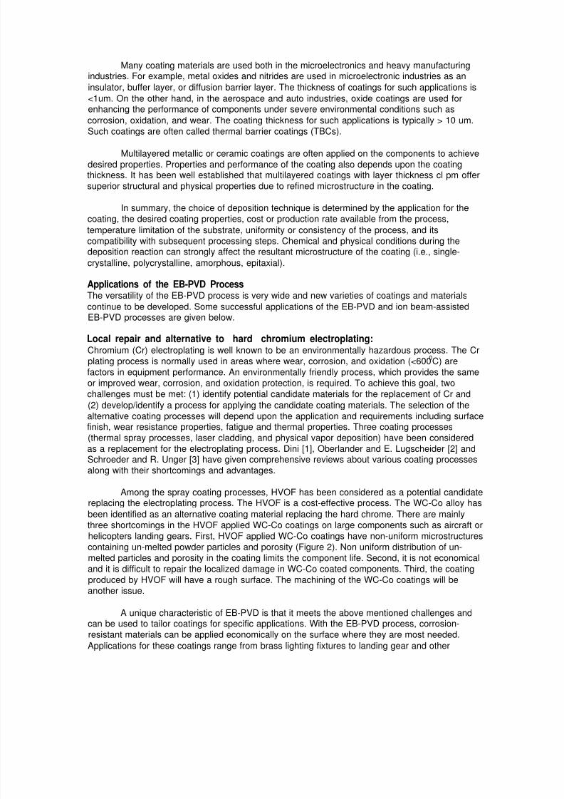
helicopters landing gears. First, HVOF applied WC-Co coatings have non-uniform microstructures
containing un-melted powder particles and porosity (Figure 2). Non uniform distribution of un-
melted particles and porosity in the coating limits the component life. Second, it is not economicaland it is difficult to repair the localized damage in WC-Co coated components. Third, the coating
produced by HVOF will have a rough surface. The machining of the WC-Co coatings will be
another issue.
A unique characteristic of EB-PVD is that it meets the above mentioned challenges andcan be used to tailor coatings for specific applications. With the EB-PVD process, corrosion-
resistant materials can be applied economically on the surface where they are most needed.
Applications for these coatings range from brass lighting fixtures to landing gear and other
7/31/2019 Ebeam Deposition
http://slidepdf.com/reader/full/ebeam-deposition 6/16
components of aircraft and helicopters. IBAD, EB-PVD process offers additional flexibility in
repairing localized damage in landing gears which cannot be done by any other processes
Figure 2. Low (a) high (b) magnification SEM micrographs of WC-Co coatings deposited by HVOFshowing non-uniform microstructure and porosity.
without affecting the physical and mechanical properties of the base material. The significant
advantage of using IBAD along with EB-PVD is enhancing metallurgical bonding of the coating
with the substrate at a relatively low temperature. For instance, EB-PVD chromium coatings were
flaking or debonding from the landing gear when deposited below 280 0C (<550 OF). This was
perhaps due to poor metallurgical bonding and high residual stresses in the deposit. When, the
same Cr coating was applied on the landing gear along with argon ion bombardment (Table 2),
the resulting coating had a dense microstructure with good metallurgical bonding between the
base material as well as the electroplated chromium (region b of Figure 38).
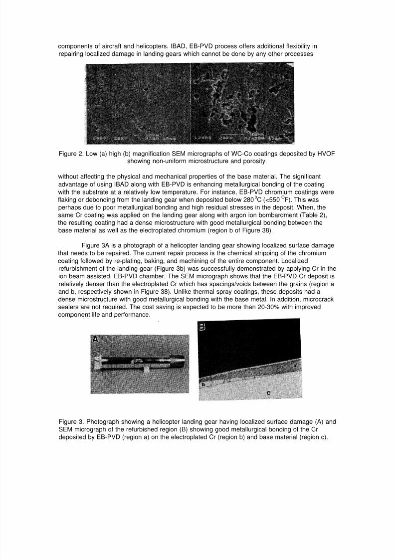
Figure 3A is a photograph of a helicopter landing gear showing localized surface damage
that needs to be repaired. The current repair process is the chemical stripping of the chromium
coating followed by re-plating, baking, and machining of the entire component. Localized
refurbishment of the landing gear (Figure 3b) was successfully demonstrated by applying Cr in the
ion beam assisted, EB-PVD chamber. The SEM micrograph shows that the EB-PVD Cr deposit is
relatively denser than the electroplated Cr which has spacings/voids between the grains (region a
and b, respectively shown in Figure 38). Unlike thermal spray coatings, these deposits had adense microstructure with good metallurgical bonding with the base metal. In addition, microcrack
sealers are not required. The cost saving is expected to be more than 20-30% with improved
component life and performance.
Figure 3. Photograph showing a helicopter landing gear having localized surface damage (A) and
SEM micrograph of the refurbished region (B) showing good metallurgical bonding of the Cr
deposited by EB-PVD (region a) on the electroplated Cr (region b) and base material (region c).
7/31/2019 Ebeam Deposition
http://slidepdf.com/reader/full/ebeam-deposition 7/16
Table 2. Process parameters used in depositing Cr by Sciaky IBAD, EB-PVD.
EB-voltage (kV) 17
EB-Current (mAmp) 900
Deposition rate (um/hour) 15
Substrate temperature (0C) <280
Deposition time (hours) 2
Ion gun parameters: 250 volts, 75 mAmp, 10 sccm Argon gas
Thermal barrier Coatings (TBCs) for the turbine industryThere is a continuous thrust in improving the life and performance of turbine components under
severe environmental conditions including erosion, oxidation, and corrosion [4, 51. The life of
components has been increased by applying TBCs either by plasma spray or EB-PVD processes.
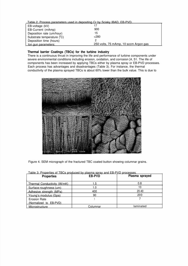
Each process has advantages and disadvantages (Table 3). For instance, the thermal
conductivity of the plasma sprayed TBCs is about 60% lower than the bulk value. This is due to
Figure 4. SEM micrograph of the fractured TBC coated button showing columnar grains.
Table 3: Properties of TBCs produced by plasma spray and EB-PVD processes.
Properties EB-PVD Plasma sprayed
Thermal Conductivity (W/mK) 1.5 0.8
Surface roughness (um) 1.0 10
Adhesive strength (MPa) 400 20-40
Young’s modulus (Gpa) 90 200
Erosion Rate 1 7
(Normalized to EB-PVD)
Microstructure Columnar laminated
7/31/2019 Ebeam Deposition
http://slidepdf.com/reader/full/ebeam-deposition 8/16
presence of porosity between the laminated grains. In contrast, the thermal conductivity of TBCs
applied by EB-PVD is higher than the plasma spray coatings. The higher thermal conductivity in
the EB-PVD TBCs is due to limited porosity present in the individual columnar grains. The porosity
in TBCs is mainly present between the columnar grains (Figure 4). In spite of higher thermal
conductivity, TBCs applied by EB-PVD is preferred over the plasma spray process due to smooth
surface finish, better strain tolerance, better erosion-resistance properties, and improved
metallurgical bonding with the substrate. The typical process parameters used in producing TBCs
are listed in Table 4.
Table 4. Process parameters used in depositing TBCs by Sciaky EB-PVD
EB-voltage (kV) 18
EB-Current (Amp) 1.7
Deposition rate (um/min) 3.4
Substrate temperature (0C) <1000
Deposition time (hours) 1
In spite of significant advancement in the EB-PVD coating technology, there are still challenges in
producing low thermal conductivity EB-PVD TBCs. Future thrusts are in producing a low-
conductivity EB-PVD TBC by altering the microstructure and creating micro-porosity within the
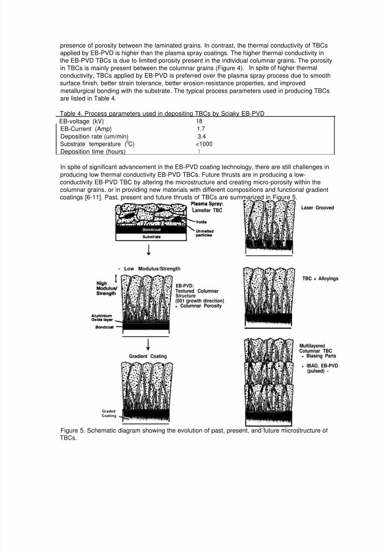
columnar grains. or in providing new materials with different compositions and functional gradientcoatings [6-11]. Past, present and future thrusts of TBCs are summarized in Figure 5.
Lamellar TBC
- Low Modulus/Strength
EB-PVD:
Textured ColumnarStructure
(001 growth direction)l Columnar Porosity
Laser Grooved
TBC + Alloyings
Gradient Coating
Graded
Coating
Figure 5. Schematic diagram showing the evolution of past, present, and future microstructure ofTBCs.
MultilayeredColumnar TBCl Biasing Parts
l IBAD, EB-PVD(pulsed) -
7/31/2019 Ebeam Deposition
http://slidepdf.com/reader/full/ebeam-deposition 9/16
Coatings for machining tools and forging die industriesMetallic borides, carbides, nitrides, and oxides have long been known to be very hard, wear-resistant materials. Applying these hard coatings to tool steels and tungsten carbide-cobalt
cutting inserts can increase the tool life by several hundred percent (400-600%), reducing costs
associated tool procurement, set-up time, and machine down time. Wear-resistant coatings are
often characterized as having high melting temperatures as well as high hardness values.
However, it is important to mention here that the coating performance depends on several factorsincluding: coating material, the deposition process and machining conditions. The deposition
process and parameters often dictate the coating’s microstructure features (i.e., grain size, degree
of texture, density, etc) and thus its properties [12-16].
Nitride coatings are commercially applied by the PVD process (Table 1) whereas carbide
coatings (such as Tic, HfC, and ZrC) are applied by CVD. Since CVD is a high-temperatureprocess (800-1200
0C), many temperature-sensitive substrates cannot be coated by this method.
EB-PVD has overcome some of the problems associated with CVD, including environmentalissues (waste of hazardous chemical gases), undesirable high-temperature reactions, and low
deposition rate. Hard coatings such as TiN, TiC, HfC, ZrC, TiN, and TiB2 have been economically
produced by ion beam-assisted EB-PVD at relatively low temperatures.
The machining of titanium and nickel-based alloys is very difficult and challenging. Toimprove the efficiency and life of cutting tools, titanium nitride and titanium carbide coatings have
been deposited by reactive ion beam assisted, electron beam physical vapor deposition (RIBA,
EB-PVD). By evaporating titanium metal and mixing the vapor with an ionized argon and nitrogen(nitride) or acetylene (carbide) mixture, near stochiometric compounds with high Vickers’
hardness values (TIN: 2500 VH 0.050 Tic: 3500 VH 0.050) were produced. These high hardness
values are attributed to the high degree of texturing. Tailoring the processing conditions in order
to achieve a specific orientation of the grains (and crystal structure), will increase the hardness aswell as the wear-resistance of the coating.
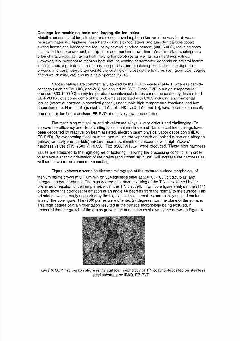
Figure 6 shows a scanning electron micrograph of the textured surface morphology of
titanium nitride grown at 0.1 um/min on 304 stainless steel at 650°C, -100 volt d.c. bias, and
nitrogen ion bombardment. The high degree of surface texturing of the TIN is explained by thepreferred orientation of certain planes within the TIN unit cell. From pole figure analysis, the (111)
planes show the strongest orientation at an angle 44 degrees from the normal to the surface. Thisorientation was strongly supported by the highly localized intensities and closely spaced contour
lines of the pole figure. The (200) planes were oriented 27 degrees from the plane of the surface.
This high degree of grain orientation resulted in the surface morphology being textured. It
appeared that the growth of the grains grew in the orientation as shown by the arrows in Figure 6.
Figure 6: SEM micrograph showing the surface morphology of TiN coating deposited on stainless
steel substrate by IBAD, EB-PVD.
7/31/2019 Ebeam Deposition
http://slidepdf.com/reader/full/ebeam-deposition 10/16
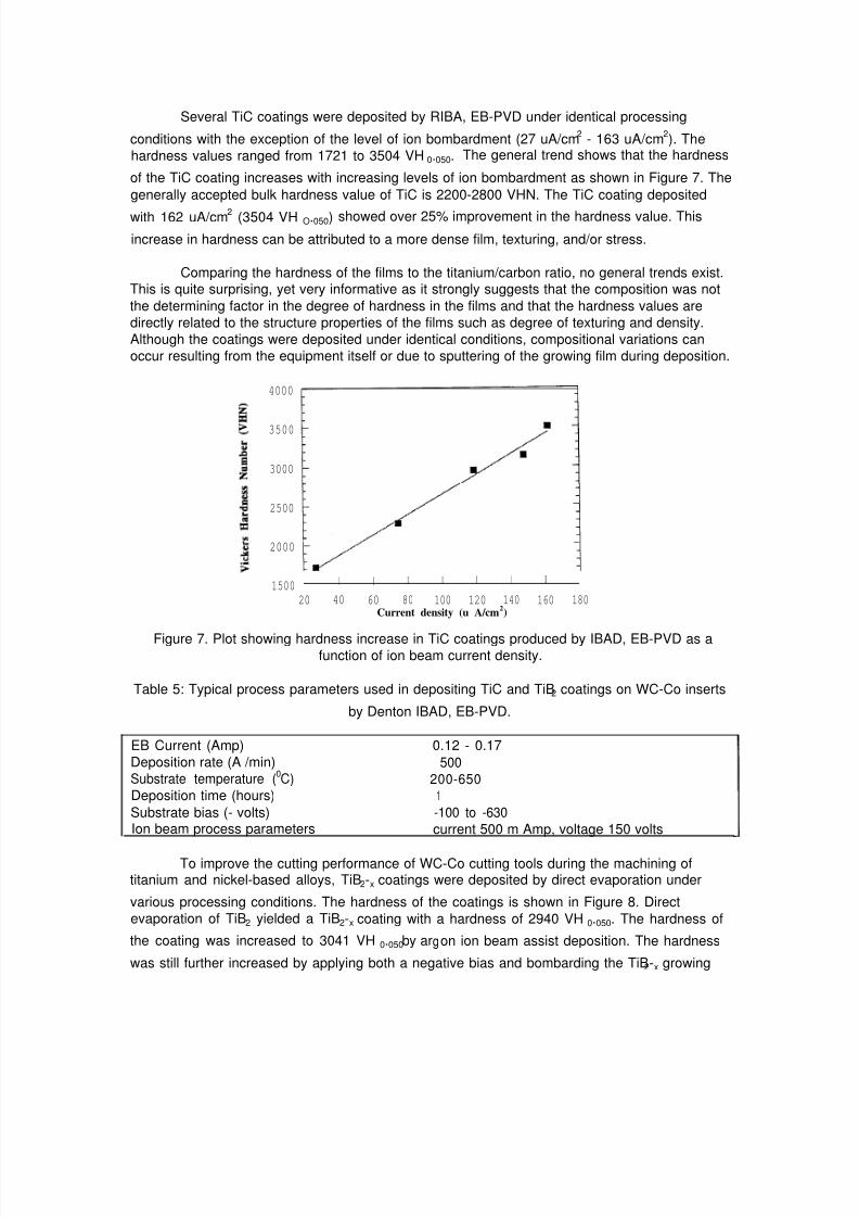
Several TiC coatings were deposited by RIBA, EB-PVD under identical processing
conditions with the exception of the level of ion bombardment (27 uA/cm2
- 163 uA/cm2). The
hardness values ranged from 1721 to 3504 VH 0.050. The general trend shows that the hardness
of the TiC coating increases with increasing levels of ion bombardment as shown in Figure 7. The
generally accepted bulk hardness value of TiC is 2200-2800 VHN. The TiC coating deposited
with 162 uA/cm2 (3504 VH O.050) showed over 25% improvement in the hardness value. This
increase in hardness can be attributed to a more dense film, texturing, and/or stress.
Comparing the hardness of the films to the titanium/carbon ratio, no general trends exist.This is quite surprising, yet very informative as it strongly suggests that the composition was not
the determining factor in the degree of hardness in the films and that the hardness values are
directly related to the structure properties of the films such as degree of texturing and density.
Although the coatings were deposited under identical conditions, compositional variations can
occur resulting from the equipment itself or due to sputtering of the growing film during deposition.
4000
3500
3000
2500
2000
1500I I I I I I I
20 40 60 80 100 120 140 160 180
Current density (u A/cm2)
Figure 7. Plot showing hardness increase in TiC coatings produced by IBAD, EB-PVD as afunction of ion beam current density.
Table 5: Typical process parameters used in depositing TiC and TiB2 coatings on WC-Co inserts
by Denton IBAD, EB-PVD.
EB Current (Amp) 0.12 - 0.17
Deposition rate (A /min) 500Substrate temperature (0C) 200-650Deposition time (hours) 1
Substrate bias (- volts) -100 to -630Ion beam process parameters current 500 m Amp, voltage 150 volts
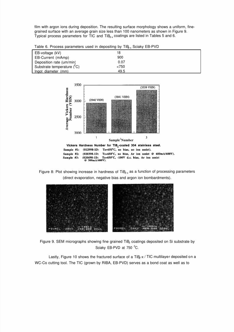
To improve the cutting performance of WC-Co cutting tools during the machining oftitanium and nickel-based alloys, TiB2-x coatings were deposited by direct evaporation under
various processing conditions. The hardness of the coatings is shown in Figure 8. Direct
evaporation of TiB2 yielded a TiB2-x coating with a hardness of 2940 VH 0.050. The hardness of
the coating was increased to 3041 VH 0.050 yb argon ion beam assist deposition. The hardness
was still further increased by applying both a negative bias and bombarding the TiB2-x growing
7/31/2019 Ebeam Deposition
http://slidepdf.com/reader/full/ebeam-deposition 11/16
film with argon ions during deposition. The resulting surface morphology shows a uniform, fine-
grained surface with an average grain size less than 100 nanometers as shown in Figure 9.
Typical process parameters for TIC and TiB2-x coatings are listed in Tables 5 and 6.
Table 6. Process parameters used in depositing by TiB2-x Sciaky EB-PVD
EB-voltage (kV) 18
EB-Current (mAmp) 900Deposition rate (um/min) 0.07
Substrate temperature (0C) <750
Ingot diameter (mm) 49.5
1
Sample2Number
3
Figure 8: Plot showing increase in hardness of TiB2-x as a function of processing parameters
(direct evaporation, negative bias and argon ion bombardments).
Figure 9. SEM micrographs showing fine grained TiB2 coatings deposited on Si substrate by
Sciaky EB-PVD at 7500C.
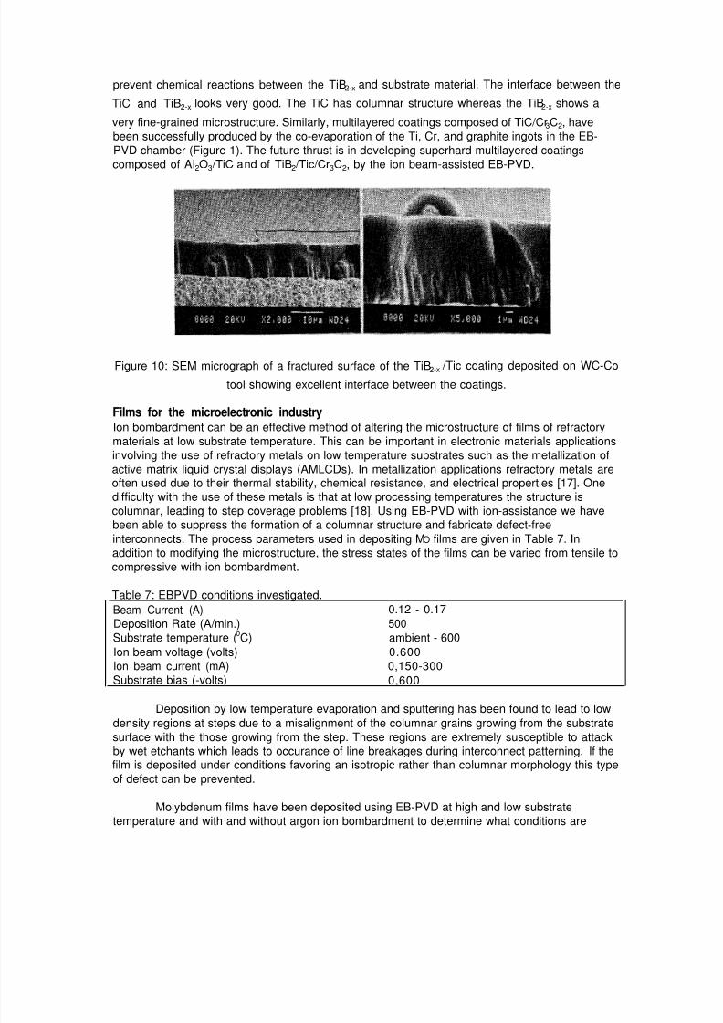
Lastly, Figure 10 shows the fractured surface of a TiB2-x / TIC multilayer deposited on a
WC-Co cutting tool. The TIC (grown by RIBA, EB-PVD) serves as a bond coat as well as to
7/31/2019 Ebeam Deposition
http://slidepdf.com/reader/full/ebeam-deposition 12/16
prevent chemical reactions between the TiB2-x and substrate material. The interface between the
TiC and TiB2-x looks very good. The TiC has columnar structure whereas the TiB2-x shows a
very fine-grained microstructure. Similarly, multilayered coatings composed of TiC/Cr3C2, have
been successfully produced by the co-evaporation of the Ti, Cr, and graphite ingots in the EB-
PVD chamber (Figure 1). The future thrust is in developing superhard multilayered coatings
composed of AI2O3 /TiC and of TiB2 /Tic/Cr3C2, by the ion beam-assisted EB-PVD.
Figure 10: SEM micrograph of a fractured surface of the TiB2-x /Tic coating deposited on WC-Co
tool showing excellent interface between the coatings.
Films for the microelectronic industryIon bombardment can be an effective method of altering the microstructure of films of refractory
materials at low substrate temperature. This can be important in electronic materials applications
involving the use of refractory metals on low temperature substrates such as the metallization of
active matrix liquid crystal displays (AMLCDs). In metallization applications refractory metals areoften used due to their thermal stability, chemical resistance, and electrical properties [17]. Onedifficulty with the use of these metals is that at low processing temperatures the structure is
columnar, leading to step coverage problems [18]. Using EB-PVD with ion-assistance we have
been able to suppress the formation of a columnar structure and fabricate defect-free
interconnects. The process parameters used in depositing MO films are given in Table 7. Inaddition to modifying the microstructure, the stress states of the films can be varied from tensile to
compressive with ion bombardment.
Table 7: EBPVD conditions investigated.
Beam Current (A)Deposition Rate (A/min.)
Substrate temperature (0C)
Ion beam voltage (volts)
Ion beam current (mA)
Substrate bias (-volts)
0.12 - 0.17
500
ambient - 600
0.600
0,150-300
0,600
Deposition by low temperature evaporation and sputtering has been found to lead to low
density regions at steps due to a misalignment of the columnar grains growing from the substrate
surface with the those growing from the step. These regions are extremely susceptible to attack
by wet etchants which leads to occurance of line breakages during interconnect patterning. If thefilm is deposited under conditions favoring an isotropic rather than columnar morphology this type
of defect can be prevented.
Molybdenum films have been deposited using EB-PVD at high and low substrate
temperature and with and without argon ion bombardment to determine what conditions are
7/31/2019 Ebeam Deposition
http://slidepdf.com/reader/full/ebeam-deposition 13/16
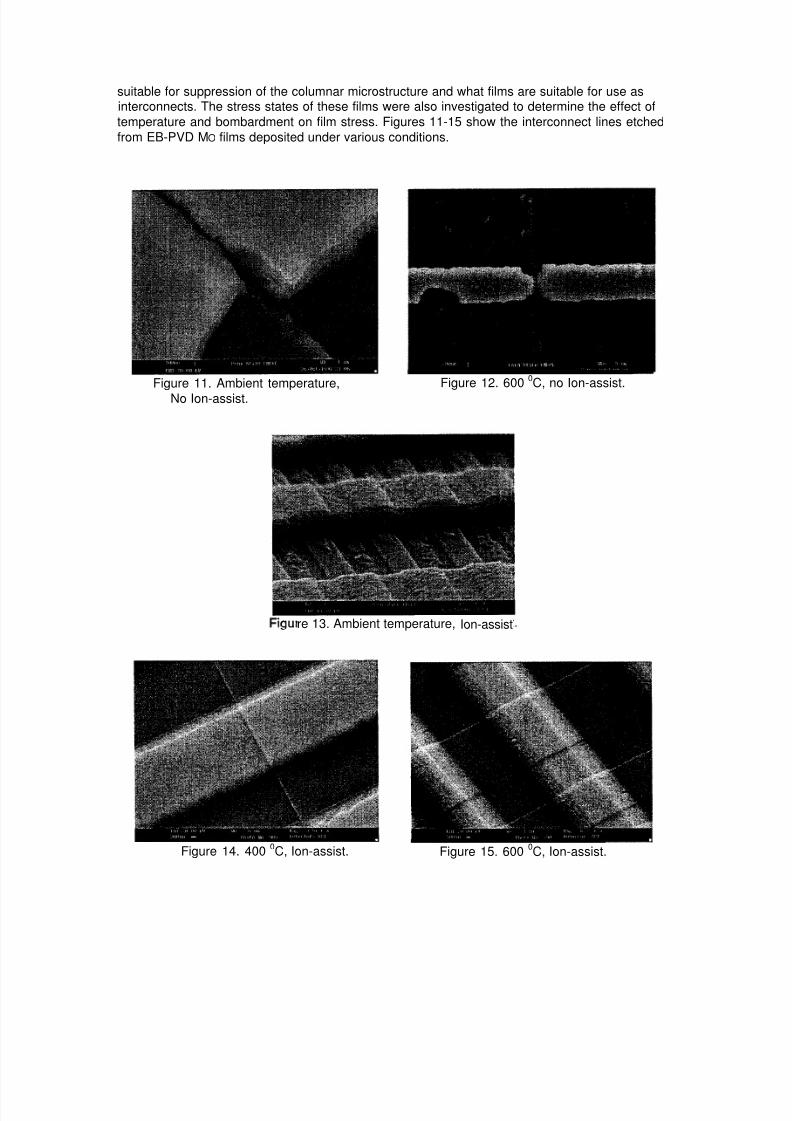
suitable for suppression of the columnar microstructure and what films are suitable for use asinterconnects. The stress states of these films were also investigated to determine the effect of
temperature and bombardment on film stress. Figures 11-15 show the interconnect lines etched
from EB-PVD MO films deposited under various conditions.
Figure 11. Ambient temperature,
No Ion-assist.
Figure 12. 600 0C, no Ion-assist.
re 13. Ambient temperature, Ion-assist
Figure 14. 400 0C, Ion-assist. Figure 15. 6000C, Ion-assist.
7/31/2019 Ebeam Deposition
http://slidepdf.com/reader/full/ebeam-deposition 14/16
Of these films, the ones showing the least amount of preferential etching were those deposited
under high bombardment and concurrent substrate heating as shown in Figures 14 and 15. The
film evaporated with no substrate heating or bombardment is particularly poor due to weak
adhesion of the film to the substrate (Figure. 11). It appears that bombardment or temperature
alone is unable to sufficiently alter the microstructure of the MO film as shown by Figs. 12 and 13;however, the combination of the two is sufficient to suppress the formation of the columnar
microstructure leading to step induced defects.
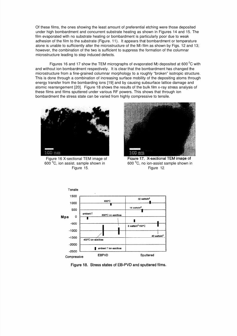
Figures 16 and 17 show the TEM micrographs of evaporated MO deposited at 6000C with
and without ion bombardment respectively. It is clear that the bombardment has changed the
microstructure from a fine-grained columnar morphology to a roughly “broken” isotropic structure.
This is done through a combination of increasing surface mobility of the depositing atoms through
energy transfer from the bombarding ions [19] and by causing subsurface lattice damage and
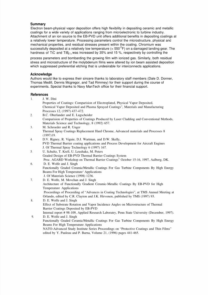
atomic rearrangement [20]. Figure 18 shows the results of the bulk film x-ray stress analysis of
these films and films sputtered under various RF powers. This shows that through ionbombardment the stress state can be varied from highly compressive to tensile.
Figure 16 X-sectional TEM image of
600 0C, ion assist. sample shown in
Figure 15.
600 0C, no ion-assist sample shown in
Figure 12.
7/31/2019 Ebeam Deposition
http://slidepdf.com/reader/full/ebeam-deposition 15/16
SummaryElectron beam-physical vapor deposition offers high flexibility in depositing ceramic and metallic
coatings for a wide variety of applications ranging from microelectronic to turbine industry.
Attachment of an ion source to the EB-PVD unit offers additional benefits in depositing coatings at
a relatively lower temperature. Processing parameters control the microstructure, physical and
mechanical properties, and residual stresses present within the coating. Chromium was
successfully deposited at a relatively low temperature (< 550OF) on a damaged landing gear. The
hardness of TiC and TiB2-x was increased by 35% and 15 %, respectively by controlling the
process parameters and bombarding the growing film with ionized gas. Similarly, both residual
stress and microstructure of the molybdenum films were altered by ion beam assisted depositionwhich suppressed preferential etching that is undesirable for interconnects applications.
AcknowledgeAuthors would like to express their sincere thanks to laboratory staff members (Dale D. Donner,Thomas Medill, Dennis Mcgregor, and Tad Rimmey) for their support during the course of
experiments. Special thanks to Navy ManTech office for their financial support.
References1. J. W. Dini
2.
3.
4.
5.
6.
7.
8.
9.
Properties of Coatings: Comparision of Electroplated, Physical Vapor Deposited,Chemical Vapor Deposited and Plasma Sprayed Coatings”, Materials and Manufacturing
Processes 12, (1997) 437-472.
B.C. Oberlander and E. Lugscheider
Comparision of Properties of Coatings Produced by Laser Cladding and Conventional Methods,
Materials Science and Technology, 8 (1992) 657.
M. Schroeder and R. Unger
Thermal Spray Coatings Replacement Hard Chrome, Advanced materials and Processes 8
(1997)19.
D.V. Rigney, R. Viguie, D.J. Wartman, and D.W. Skelly,
PVD Thermal Barrier coating applications and Process Development for Aircraft Engines
J. Of Thermal Spray Technology 6 (1997) 167.
U. Schultz, T. Krell, U. Leushake, M. Peters
Graded Design of EB-PVD Thermal Barrier Coatings SystemProc. AGARD Workshop on Thermal Barrier Coatings” October 15-16, 1997, Aalborg, DK.
D. E. Wolfe and J. Singh
Functionally Graded Ceramic/Metallic Coatings For Gas Turbine Components By High Energy
Beams For High Temperature‘ Applications
J. Of Materials Science (1998) 1236.
D. E. Wolfe, M. Movchan and J. Singh
Architecture of Functionally Gradient Ceramic-Metallic Coatings By EB-PVD for High
Temperature Applications
Proceedings of Proceeding of “Advances in Coating Technologies”, at TMS Annual Meeting at
Orlando, edited by C.R. Clayton and J.K. Hirvonen, published by TMS (1997) 93.
D. E. Wolfe and J. Singh
Effect of Substrate Rotation and Vapor Incidence Angles on Microstructure of Thermal
Barrier Coatings Deposited by EB-PVD
Internal report # 98-109, Applied Research Laboratry, Penn State University (December, 1997).
D. E. Wolfe and J. Singh
Functionally Graded Ceramic/Metallic Coatings For Gas Turbine Components By High Energy
Beams For High Temperature Applications
NATO-Advanced Study Institute Series Proceedings on “Protective Coatings and Thin Films”
edited by Y. Pauleau and P. Barna, Volume 21, (1996) pages 441-465.
7/31/2019 Ebeam Deposition
http://slidepdf.com/reader/full/ebeam-deposition 16/16
10.
11.
12.
13.
14.
15.
17.
Structure and Properties of TiN Coatings
Thin Solid Films, 128 (1985) 45-55.
D. E. Wolfe and J. Singh
Microstructural Evoluation of Titanium Nitride (TiN) Coatings Produced by by Reactive Ion
Beam-Assisted, Electron Beam-Physical Vapor Deposition (RIBA, EB-PVD)
J. of Materials Science (1998-in press)
18. P. L. Shah, IEEE Trans. Electron. Dev., ED-26,631 (1979).
19. K. Kato and T. Wada, Mat. Res. Soc. Symp. Proc. 18 1,27 (1990).
20 R. Messier, J. Vat. Sci Technol. A4,490 (1986).
21 C. W. Allen and E. A. Ryan, Mat. Res. Soc. Symp. Proc. 439,277 (1997).
J. Singh
Ion Beam Assisted, Electron Beam Physical Vapor Deposition, Advanced Materials and Process
11 (1996) 32.
M. Movchan and J. Singh
Development of Multi-component Coatings by EB-PVD Functionally Graded Ceramic Coatings,
Proceedings of the EB-PVD Workshop at Penn State University, edited by J. Singh and Boris
Movchan (September, 1996).
D. E. Wolfe
Growth of TiN coatings by Reactive Ion Beam-Assisted, Electron Beam-Physical Vapor
Deposition (RIBA, EB-PVD) and hard Coatings Evaluation
MS Thesis, Penn state University, University Park, PA (1996).
R. Hatschek, Coatings: Revolution in HSS Tools
American Machinist, (1983) 129-144.
J. Sundgren et al.,
Mechanisms of Reactive Sputtering of Titanium Nitride and Titanium Carbide,
Thin Solid Films, 105 (1983) 353-366.
J. Sundgren,


