
EE194-EE290C28nmSoCforIoT
Ref:Communica:onSystemsbyA.BruceCarlson,PaulB.CrillyandJanetC.RutledgeCMOSVLSIDesignbyNeilH.WesteandDavidMoneyHarrisTimingLibraryFormatReference,CadenceDesignSystemhSps://www.csee.umbc.edu/~cpatel2/links/641/slides/lect05_LIB.pdfSynopsysDesignCompilerUserGuide

Synchroniza:onBitSynchroniza:onCarrierFrequencyandPhaseFrameSynchroniza:on

Synchroniza:onPNsequencegenerator.
m1 m2 m3 m4 m51 1 1 1 1
+
Output sequence
111010...

Synchroniza:onAutocorrela:onofaPNsequence.
τNTc
Tc
Rs(τ)1
-Tc(N-1)Tc (N+1)Tc
1/N
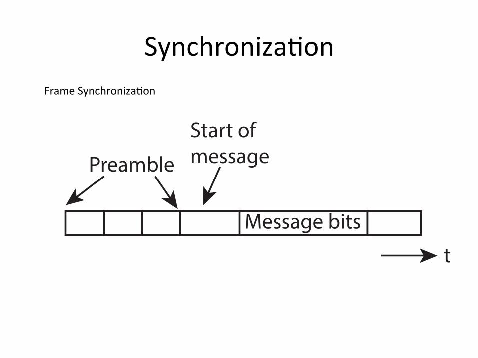
Synchroniza:onFrameSynchroniza:on
Preamble
Start ofmessage
Message bitst
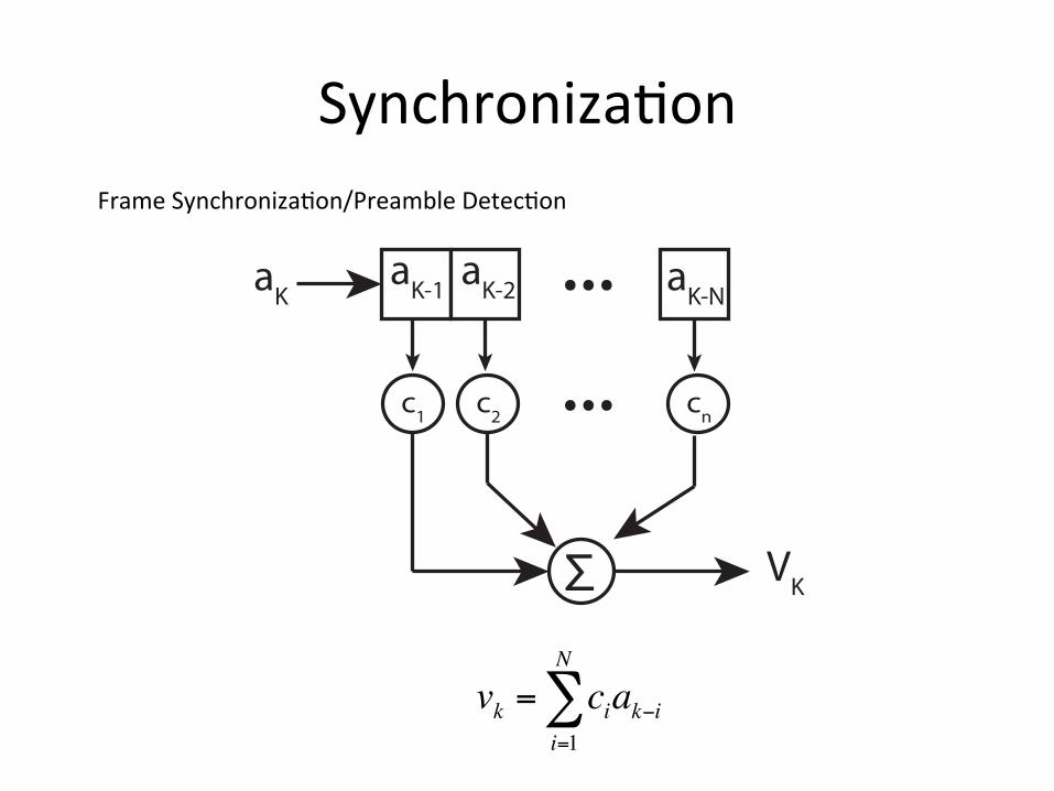
Synchroniza:onFrameSynchroniza:on/PreambleDetec:on
aK aK-1 aK-2 aK-N...c1 c2 cn...
Σ VK
vk = cii=1
N
∑ ak−i

MatlabExample
openExample('comm/MSKSignalRecoveryExample')MSKSignalRecoveryExample

TransmissionGateMuxq Nonrestoring mux uses two transmission gates
- Only 4 transistors
S
S
D0
D1YS

DLatchq When CLK = 1, latch is transparent
- D flows through to Q like a buffer q When CLK = 0, the latch is opaque
- Q holds its old value independent of D q a.k.a. transparent latch or level-sensitive latch
CLK
D Q
Latch D
CLK
Q

DLatchDesignq Multiplexer chooses D or old Q
1
0
D
CLK
QCLK
CLKCLK
CLK
DQ Q
Q

DLatchOpera:on
CLK = 1
D Q
Q
CLK = 0
D Q
Q
D
CLK
Q
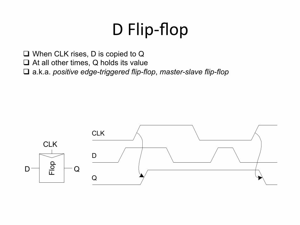
DFlip-flopFlop
CLK
D Q
D
CLK
Q
q When CLK rises, D is copied to Q q At all other times, Q holds its value q a.k.a. positive edge-triggered flip-flop, master-slave flip-flop

DFlip-flopDesignq Built from master and slave D latches
QMCLK
CLKCLK
CLK
Q
CLK
CLK
CLK
CLK
D
Latch
Latch
D QQM
CLK
CLK
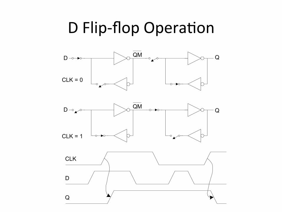
DFlip-flopOpera:on
CLK = 1
D
CLK = 0
Q
D
QM
QMQ
D
CLK
Q

RaceCondi:on
CLK1
D Q1
Flop
Flop
CLK2
Q2
CLK1
CLK2
Q1
Q2
q Back-to-back flops can malfunction from clock skew - Second flip-flop fires late - Sees first flip-flop change and captures its result - Called hold-time failure or race condition

SetupandHoldTime
Time
Volta
ge
Clock Setup Time
Hold Time

Non-overlappingClocksq Non-overlapping clocks can prevent races
- As long as non-overlap exceeds clock skew q We will use them in this class for safe design
- Industry manages skew more carefully instead
φ1
φ1φ1
φ1
φ2
φ2φ2
φ2
φ2
φ1
QMQD
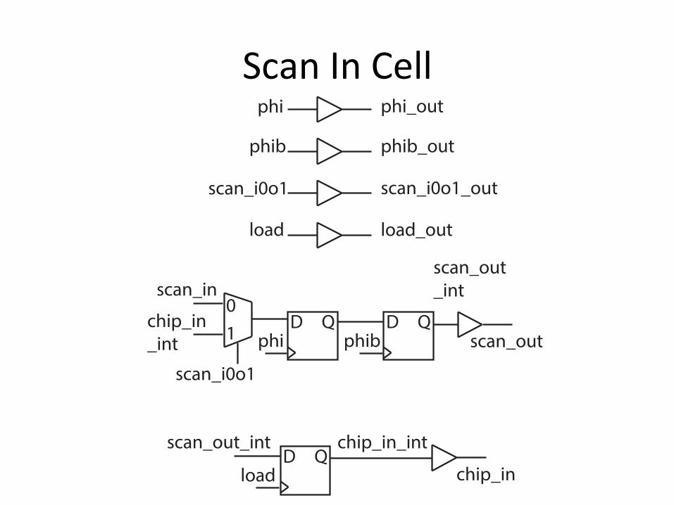
ScanInCell
D Q D Q
phi
phib
scan_i0o1
load
phi_out
phib_out
scan_i0o1_out
load_out
scan_in
chip_in_int
scan_i0o1
phi phib
01 scan_out
scan_out_int
D Qload chip_in
scan_out_int chip_in_int

ScanOutCell
D Q D Q
phi
phib
scan_i0o1
load
phi_out
phib_out
scan_i0o1_out
load_out
scan_in
chip_out
scan_i0o1
phi phib
01 scan_out

ScanIn-OutCell
D Q D Q
phi
phib
scan_i0o1
load
phi_out
phib_out
scan_i0o1_out
load_out
scan_in
chip_out
scan_i0o1
phi phib
01 scan_out
scan_out_int
D Qload chip_in
scan_out_int chip_in_int

GateLayoutq Layout can be very time consuming
- Design gates to fit together nicely - Build a library of standard cells
q Standard cell design methodology - VDD and GND should abut (standard height) - Adjacent gates should satisfy design rules - nMOS at bottom and pMOS at top - All gates include well and substrate contacts

StandardCellsq Uniform cell height q Uniform well height q M1 VDD and GND rails q M2 Access to I/Os q Well / substrate taps q Exploits regularity

CopingWithComplexityq How to design System-on-Chip?
- Many millions (even billions!) of transistors - Tens to hundreds of engineers
q Structured Design q Design Partitioning

StructuredDesignq Hierarchy: Divide and Conquer
- Recursively system into modules q Regularity
- Reuse modules wherever possible - Ex: Standard cell library
q Modularity: well-formed interfaces - Allows modules to be treated as black boxes
q Locality - Physical and temporal

DesignPar::oningq Architecture: User’s perspective, what does it do?
- Instruction set, registers - MIPS, x86, Alpha, PIC, ARM, …
q Microarchitecture - Single cycle, multi-cycle, pipelined, superscalar?
q Logic: how are functional blocks constructed - Ripple carry, carry look-ahead, carry select adders
q Circuit: how are transistors used - Complementary CMOS, pass transistors, domino
q Physical: chip layout - Datapaths, memories, random logic

HDLq Hardware Description Languages
- Widely used in logic design - Verilog and VHDL
q Describe hardware using code - Document logic functions - Simulate logic before building - Synthesize code into gates and layout
• Requires a library of standard cells

VerilogExamplemodule fulladder(input a, b, c, output s, cout); sum s1(a, b, c, s); carry c1(a, b, c, cout); endmodule module carry(input a, b, c, output cout) assign cout = (a&b) | (a&c) | (b&c); endmodule
a b
c
s
cout carrysum
s
a b c
cout
fulladder
CircuitDesignq How should logic be implemented?
- NANDs and NORs vs. ANDs and ORs? - Fan-in and fan-out? - How wide should transistors be?
q These choices affect speed, area, power q Logic synthesis makes these choices for you
- Good enough for many applications - Hand-crafted circuits are still better

Example:CarryLogic
ab
ac
bc
cout
x
y
z
g1
g2
g3
g4
a b
c
c
a b
b
a
a
b
coutcn
n1 n2
n3
n4
n5 n6
p6p5
p4
p3
p2p1
i1
i3
i2
i4
q assign cout = (a&b) | (a&c) | (b&c);
Transistors? Gate Delays?

GateLevelNetlist
ab
ac
bc
cout
x
y
z
g1
g2
g3
g4
module carry(input a, b, c, output cout) wire x, y, z; and g1(x, a, b); and g2(y, a, c); and g3(z, b, c); or g4(cout, x, y, z);endmodule

TransistorLevelNetlist
a b
c
c
a b
b
a
a
b
coutcn
n1 n2
n3
n4
n5 n6
p6p5
p4
p3
p2p1
i1
i3
i2
i4
module carry(input a, b, c, output cout) wire i1, i2, i3, i4, cn; tranif1 n1(i1, 0, a); tranif1 n2(i1, 0, b); tranif1 n3(cn, i1, c); tranif1 n4(i2, 0, b); tranif1 n5(cn, i2, a); tranif0 p1(i3, 1, a); tranif0 p2(i3, 1, b); tranif0 p3(cn, i3, c); tranif0 p4(i4, 1, b); tranif0 p5(cn, i4, a); tranif1 n6(cout, 0, cn); tranif0 p6(cout, 1, cn);endmodule

SPICENetlist.SUBCKT CARRY A B C COUT VDD GND MN1 I1 A GND GND NMOS W=1U L=0.18U AD=0.3P AS=0.5P MN2 I1 B GND GND NMOS W=1U L=0.18U AD=0.3P AS=0.5P MN3 CN C I1 GND NMOS W=1U L=0.18U AD=0.5P AS=0.5P MN4 I2 B GND GND NMOS W=1U L=0.18U AD=0.15P AS=0.5P MN5 CN A I2 GND NMOS W=1U L=0.18U AD=0.5P AS=0.15P MP1 I3 A VDD VDD PMOS W=2U L=0.18U AD=0.6P AS=1 P MP2 I3 B VDD VDD PMOS W=2U L=0.18U AD=0.6P AS=1P MP3 CN C I3 VDD PMOS W=2U L=0.18U AD=1P AS=1P MP4 I4 B VDD VDD PMOS W=2U L=0.18U AD=0.3P AS=1P MP5 CN A I4 VDD PMOS W=2U L=0.18U AD=1P AS=0.3P MN6 COUT CN GND GND NMOS W=2U L=0.18U AD=1P AS=1P MP6 COUT CN VDD VDD PMOS W=4U L=0.18U AD=2P AS=2P CI1 I1 GND 2FF CI3 I3 GND 3FF CA A GND 4FF CB B GND 4FF CC C GND 2FF CCN CN GND 4FF CCOUT COUT GND 2FF .ENDS

PhysicalDesignq Floorplan q Standard cells
- Place & route q Datapaths
- Slice planning q Area estimation

MIPSFloorplan

MIPSLayout

SynthesizedControllerq Synthesize HDL into gate-level netlist q Place & Route using standard cell library

DesignVerifica:onq Fabrication is slow & expensive q Debugging chips is very hard
- Limited visibility into operation q Prove design is right before building!
- Logic simulation - Ckt. simulation / formal verification - Layout vs. schematic comparison - Design & electrical rule checks
q Verification is > 50% of effort on most chips!
Specification
ArchitectureDesign
LogicDesign
CircuitDesign
PhysicalDesign
=
=
=
=
Function
Function
Function
FunctionTimingPower

VLSIFlowq Design Compiler (DC) Synopsys tool
DesignCompilerop:mizesdesignstoprovidethesmallestandfastestlogicalrepresenta:onofagivenfunc:on.ItcomprisestoolsthatsynthesizeyourHDLdescrip:onsintoop:mized,technology-dependent,gate-leveldesigns.
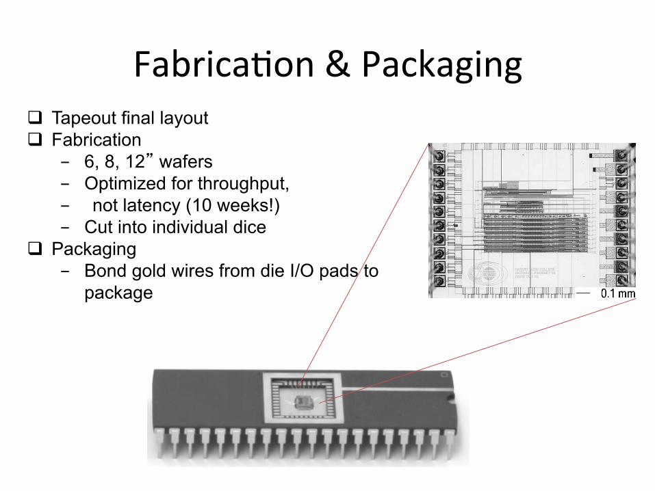
Fabrica:on&Packagingq Tapeout final layout q Fabrication
- 6, 8, 12” wafers - Optimized for throughput, - not latency (10 weeks!) - Cut into individual dice
q Packaging - Bond gold wires from die I/O pads to
package
Tes:ngq Test that chip operates
- Design errors - Manufacturing errors
q A single dust particle or wafer defect kills a die - Yields from 90% to < 10% - Depends on die size, maturity of process - Test each part before shipping to customer

MIPSR3000Processorq 32-bit 2nd generation commercial processor (1988) q Led by John Hennessy (Stanford, MIPS Founder) q 32-64 KB Caches q 1.2 µm process q 111K Transistors q Up to 12-40 MHz q 66 mm2 die q 145 I/O Pins q VDD = 5 V q 4 Watts q SGI Workstations
http://gecko54000.free.fr/?documentations=1988_MIPS_R3000

TransistorasSwitches
gs
d
g = 0
s
d
g = 1
s
d
gs
d
s
d
s
d
nMOS
pMOS
OFF ON
ON OFF
q We can view MOS transistors as electrically controlled switches q Voltage at gate controls path from source to drain

CMOSInverter
VDD
A Y
GND
A Y
0 1
1 0
A Y

CMOSNANDGate
A B Y
0 0 1
0 1 1
1 0 1
1 1 0 A
B
Y

CMOSNORGate
A B Y
0 0 1
0 1 0
1 0 0
1 1 0
A
BY

ComplementaryCMOSq Complementary CMOS logic gates
- nMOS pull-down network - pMOS pull-up network - a.k.a. static CMOS pMOS
pull-upnetwork
outputinputs
nMOSpull-downnetworkPull-up OFF Pull-up ON
Pull-down OFF Z (float) 1
Pull-down ON 0 X (crowbar)

SeriesandParallelq nMOS: 1 = ON q pMOS: 0 = ON q Series: both must be ON q Parallel: either can be ON (a)
a
b
a
b
g1
g2
0
0
a
b
0
1
a
b
1
0
a
b
1
1
OFF OFF OFF ON
(b)
a
b
a
b
g1
g2
0
0
a
b
0
1
a
b
1
0
a
b
1
1
ON OFF OFF OFF
(c)
a
b
a
b
g1 g2 0 0
OFF ON ON ON
(d) ON ON ON OFF
a
b
0
a
b
1
a
b
11 0 1
a
b
0 0
a
b
0
a
b
1
a
b
11 0 1
a
b
g1 g2

Conduc:onComplementq Complementary CMOS gates always produce 0 or 1 q Ex: NAND gate
- Series nMOS: Y=0 when both inputs are 1 - Thus Y=1 when either input is 0 - Requires parallel pMOS
q Rule of Conduction Complements - Pull-up network is complement of pull-down - Parallel -> series, series -> parallel
A
B
Y

SignalStrengthq Strength of signal
- How close it approximates ideal voltage source q VDD and GND rails are strongest 1 and 0 q nMOS pass strong 0
- But degraded or weak 1 q pMOS pass strong 1
- But degraded or weak 0 q Thus nMOS are best for pull-down network

PassTransistorsq Transistors can be used as switches
g = 0s d
g = 1s d
0 strong 0Input Output
1 degraded 1
g = 0s d
g = 1s d
0 degraded 0Input Output
strong 1
g = 1
g = 1
g = 0
g = 01
g
s d
g
s d

TransmissionGatesq Pass transistors produce degraded outputs q Transmission gates pass both 0 and 1 well
g = 0, gb = 1a b
g = 1, gb = 0a b
0 strong 0
Input Output
1 strong 1
g
gb
a b
a bg
gb
a bg
gb
a bg
gb
g = 1, gb = 0
g = 1, gb = 0
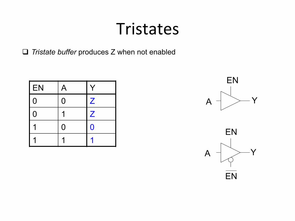
Tristatesq Tristate buffer produces Z when not enabled
EN A Y 0 0 Z 0 1 Z 1 0 0 1 1 1
A Y
EN
A Y
EN
EN
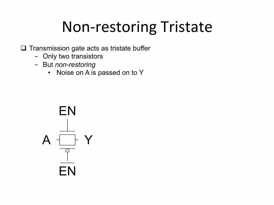
Non-restoringTristateq Transmission gate acts as tristate buffer
- Only two transistors - But non-restoring
• Noise on A is passed on to Y
A Y
EN
EN

TristateInverterq Tristate inverter produces restored output
- Violates conduction complement rule - Because we want a Z output
A
YEN
A
Y
EN = 0Y = 'Z'
Y
EN = 1Y = A
A
EN

Mul:plexersq 2:1 multiplexer chooses between two inputs
S D1 D0 Y
0 X 0 0
0 X 1 1
1 0 X 0
1 1 X 1
0
1
S
D0
D1Y

Gate-LevelMuxDesignq How many transistors are needed? 20
1 0 (too many transistors)Y SD SD= +


![Core System Package [Low Energy Controller volume]ee290c/sp18/note/BLE_Vol6.pdf · or business interruption, or for special, indirect, consequential, incidental or punitive damages,](https://cdn.vdocument.in/doc/165x107/5e8f24e2ff9cc62c5d5d853c/core-system-package-low-energy-controller-volume-ee290csp18noteblevol6pdf.jpg)