
Purdue University
NSF/DOE Thermoelectrics Partnership: Thermoelectrics for Automotive Waste Heat Recovery
Xianfan Xu (ME), Timothy Fisher (ME), Stephen Heister (AAE), Timothy Sands (MSE), Yue Wu (ChemE)
Purdue UniversityIn Partnership with General Motors Global R&D
and Oak Ridge National Laboratory

Purdue University
NSF/DOE Targeted Areas
Focused areas of this proposal: • TE Materials• Heat sink - high temperature side heat exchanger• Thermal interface materials• Metrology

Purdue University
TE Materials• Skutterudite (GM) ~ 500oC – advanced characterization on
thermal conductivity reduction (Xu)• Nanowires - room-mid temperature PbTe, Bi2Te3; and high
temperature oxide nanowires (Wu)• Metal-semiconductor superlattice (Sands)
Purdue University
Advanced Characterization of TE Materials
- Commonly used approach to increase ZT of TE materials is to the reduce the lattice thermal conductivity
- We conduct femtosecond (10-15 s) time-resolved studies of phonon scattering in thermoelectric materials to understand the fundamentals of thermal conductivity reduction
Xianfan Xu
Purdue University
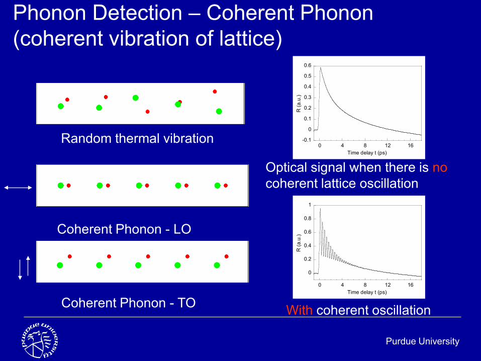
Phonon Detection – Coherent Phonon (coherent vibration of lattice)
-0.1
0
0.1
0.2
0.3
0.4
0.5
0.6
0 4 8 12 16
R (a
.u.)
Time delay t (ps)
Random thermal vibration
Optical signal when there is nocoherent lattice oscillation
0
0.2
0.4
0.6
0.8
1
0 4 8 12 16
R (a
.u.)
Time delay t (ps)
With coherent oscillation
Coherent Phonon - LO
Coherent Phonon - TO

Purdue University
Coherent Phonon Dynamics in Bi
0
1
2
3
4
5
0 4 8 12 16
∆R/R
(%)
time delay t (ps)
0
1
2
3
4
5
-0.8 0 0.8 1.6 2.4 3.2 4 4.8 5.6
ExperimentFitting
0 1 2 3 4 5 6
Am
plitu
de o
f FT
Frequency (THz)
2.88 THz
- Rise of the signal: Photon – electron/exciton (charge) coupling- Decay of the envelope of the signal: electron/exciton (charge) – phonon
coupling - heating- Phonon oscillation and dephasing: Phonon interactions with charges,
other phonon modes, impurities, physical boundaries, etc. – all important for energy transport and conversion processes
Fouriertransform
50 100 150 200
Ram
an S
igna
l (a.
u.)
Raman Shift (cm-1)
98 cm-1 (2.94 THz)
Raman

Purdue University
Filled Antimony Skutterudites
Oscillation due to filling of guest materials
Co
Purdue University
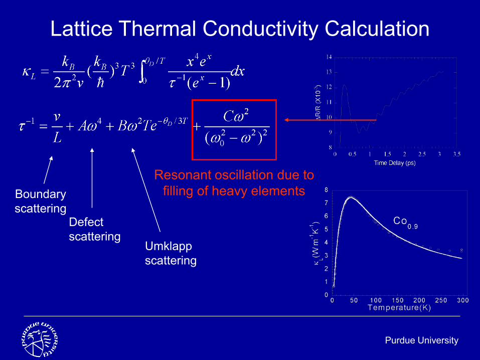
Lattice Thermal Conductivity Calculation
Boundary scattering
Defect scattering
Umklappscattering
Resonant oscillation due to filling of heavy elements

Purdue University
Misch-metal Filled Antimony Skutterudites
Nominal representation
Composition
Co0.9 (unfilled) Co0.9Fe0.1Sb3
Mm0.55 Mm0.55Fe2.44Co1.56Sb11.96
Mm0.65 Mm0.65Fe2.92Co1.08Sb11.98
Mm0.72 Mm0.72Fe3.43Co0.57Sb11.97
Mm0.82 Mm0.82Fe4Sb11.96
Mm: Ce:La:Nd:Pr:Si:Fe:Al:O = 50.75:22.75:16.22:5.72:3.35:0.72:0.50
0
1
2
3
4
1 2 3 4 5∆R
/R (X
10-3
)
Mm0.82
(b)
Mm0.72
Mm0.65
Mm0.55Co
0.9
Delay (ps)

Purdue University
- Computation of κ based on resonant oscillation model and ultrafast measurement results agree well with k value measured from ~ 0 to 300 K.
- Role of filled material: resonant vibration vs. defect generation
(Phys. Rev. Lett, 2009)

Purdue University
Phonon Scattering in Bi2Te3, Sb2Te3 and Bi2Te3/Sb2Te3 Superlattice
(in collaboration with RTI)

Purdue University
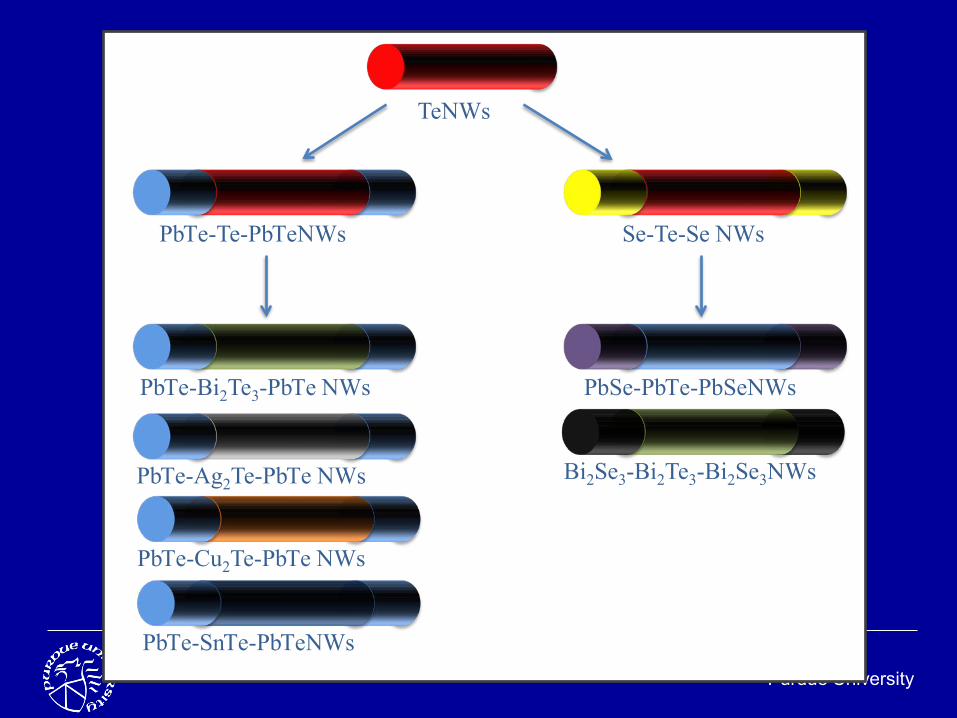
Nanowire TE Materials
Yue Wu, School of Chemical Engineering

Purdue University
Synthesis of Molecular-scale Chalcogenide Nanowires
Scalable and high yield (93%)
Purdue University
TeNWs
PbTe-Te-PbTeNWs
PbTe-Bi2Te3-PbTe NWs
Se-Te-Se NWs
PbSe-PbTe-PbSeNWs
Bi2Se3-Bi2Te3-Bi2Se3NWsPbTe-Ag2Te-PbTe NWs
PbTe-Cu2Te-PbTe NWs
PbTe-SnTe-PbTeNWs

Purdue University
Bulk-like Thermionic Energy Conversion Device Fabricated from Laminated Nanostructured Metal/Semiconductor Superlattices
100 nm100-Si
HfN/ScN
Co-PI: Tim SandsResearch Associate: Jeremy SchroederGraduate Student: Bivas Saha
100 µm2 nm
Purdue University
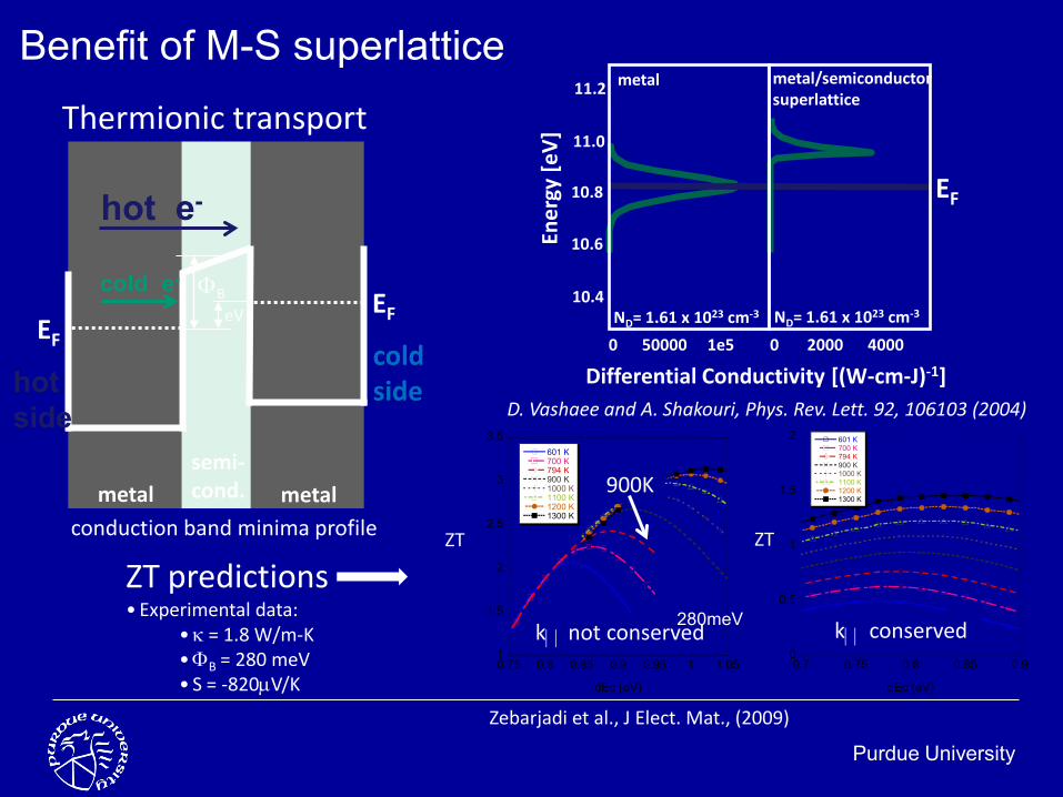
Benefit of M-S superlattice
Differential Conductivity [(W-cm-J)-1]0 2000 4000
EF
ND= 1.61 x 1023 cm-3
11.2
10.8
10.6
11.0
10.4
0 50000 1e5
ND= 1.61 x 1023 cm-3
metal metal/semiconductorsuperlattice
D. Vashaee and A. Shakouri, Phys. Rev. Lett. 92, 106103 (2004)
hot e-
cold e-
EF
EF
metal metalsemi-cond.
eV
ΦB
hotside
conduction band minima profile
coldside
Thermionic transport
Ener
gy [e
V]
Zebarjadi et al., J Elect. Mat., (2009)
1
1.5
2
2.5
3
3.5
0.75 0.8 0.85 0.9 0.95 1 1.05
601 K700 K794 K900 K1000 K1100 K1200 K1300 K
ZT
dEc (eV)
ZT
knot conserved0
0.5
1
1.5
2
0.7 0.75 0.8 0.85 0.9
601 K700 K794 K900 K1000 K1100 K1200 K1300 K
ZT
dEc (eV)
ZT
k conserved
ZT predictions• Experimental data:
•κ = 1.8 W/m-K•ΦB = 280 meV• S = -820µV/K
280meV
900K

Purdue University
Laminates
Thermal propertiesκTE = 3 W/m-K κ Au = 300 W/m-KRc,thermal ≈ 7 x 10⁻⁸ K-m2/W
Electrical propertiesρc = 1 x 10⁻⁸ Ω-cm2
ρ TE = 1 mΩ -cm ρ Au = 25 µΩ -cm
Total thickness
TE layers 50µm
Au bonding layers 20µm
93% of total thermal impedance96% of total electrical impedance
Laminate bilayers
substrate
substrate
5µm polySL
5µm polySL
Bond Etch substrateDeposit metal
1µm bonding metal
70µm
TE layers
Process requires low metal-nitride/metal-bond contact resistance

Purdue University
Bulk-like laminate
1 mm
sewingpin
• 40 thermoelectric layers (5 µm each)• 80 gold layers (1 µm each)•~300 µm x 300 µm x 280 µm• diced and polished (3 µm diamond lapping disc)
FESEM
100 µm
100 µm
100 µm
100 µm
SEM of four sides of polished cube

Purdue University
Professor Steve Heister School of Aeronautics & Astronautics
Heat Exchangers for Automotive Exhaust Applications

Purdue University
Background• Rolls-Royce established a University Technology Center
(UTC) at Purdue in 2003 to study High Mach Propulsion for aerospace applications
• A key technology to enable high Mach flight is a heat exchanger that cools some compressor exhaust gases for use in turbine blade cooling- Air temps 1000-1200F (550-650 C) pressures to 40 bar- Fuel temps to 1000F (550 C) at pressures to 90 bar
• UTC has graduated roughly 10 students working in technologies to enable a fuel/air heat exchanger for operation in difficult environments• fuel coking/thermal stability• tube/shell HEX design• plate/fin HEX design• heat transfer augmentation

Purdue University
Foil Laminate Construction
21
Chemical etching produces microscale flow passages on individual foils. The foils are then stacked, aligned, and diffusion bonded under heat and pressure.
From “Compact Superalloy Heat Exchangers for Cooled Cooling Air Applications”, G. Campbell, J Fryer, Saddleback Aerspace, Turbine Symposium Presentation ca. 2002

Purdue University
Heat Exchanger for Waste Heat Recovery
Inflow Exhaust
Fin, or Integrated Fin/TE Assembly (IFTEA)
A A’B
B’
Inflow Exhaust
Fin, or Integrated Fin/TE Assembly (IFTEA)
A A’B
B’
Coolant
TE material
Hot gas
Hot gas
Coolant
TE material
Hot gas
Hot gas
Coolant
TE material
Hot gas
Hot gasInflow
Fins
: high-T TE material: low-T TE material
CoolantThermal interface materials
Hot side heatexchangerInflow
Fins
: high-T TE material: low-T TE material
CoolantThermal interface materials
Hot side heatexchanger
And many other possible topologies (cylindrical etc.)

Purdue University
CNT Array Thermal Interfaces Materials
Timothy S. Fisher, Mechanical Engineering

Purdue University
CNT Array Thermal and Electrical Interfaces
Solid 1
Solid 2
Solid 1
Solid 2
One-sided interface Two-sided interface
Solid 1
Solid 2
Cu foil
CNT/foil interface
One-sided (post test)
5 µm
copper
silicon5 µm 100 µm

Purdue University
1
10
100
1000
0.1 0.15 0.2 0.25 0.3 0.35 0.4
Pressure (MPa)
Inte
rfac
e R
esis
tan
ce (
mm
2 K/W
) Bare Interface (1-D ref. bar)
1-Sided Interface
CNT/foil Interface
2-Sided Interface
Thermal Interface Results: Summary
References:
B.A. Cola, J. Xu, T.S. Fisher,Int J Heat Mass Transfer, 52, 3490-3503 (2009).
B.A. Cola, J. Xu, C. Cheng, H. Hu, X. Xu, and T.S. Fisher, J. Appl. Phys. 101, 054313 (2007).
B.A. Cola, X. Xu, and T.S. Fisher, Appl. Phys. Lett. 90, 093513 (2007).
J. Xu and T.S. Fisher, Int. J. Heat Mass Trans. 49, 1658 (2006).
J. Xu, T.S. Fisher, IEEE Trans. CPT, 29, 261 (2006).
silicon/copper substrates at room temperature
State-of-the-art commercial materials(non-bonded interfaces)
Target performance range

Purdue University
CNT Interfaces to Thermoelectrics
0
5
10
15
20
25
30
35
0 5 10 15 20 25
Res
ista
nce
(Ω)
Bi2Te3 film thickness (µm)
Ni - Bi2Te3structure
Ni - CNT - Bi2Te3 structure30 µm
TE film
MWCNT array
Ni - CNT - Bi2Te3 structure
Motivation• Parasitic electrical contact resistance can strongly degrade the efficiency of thermoelectric devices• Direct electrodeposited thermoelectric (Bi2Te3) on CNTs shows reduced interface resistance
Mishra et al., Adv Mat 21 4280, 2009
With Sands group

Purdue University
Improving Thermal Stability
Raidongia et al. (J. Mater. Chem. 2008, 18, 83-90) demonstrated large improvements in thermal stability of nanotubes by conversion to BC4N
Our recent work:
1 μm 1 μm
(a) (b)
MWCNT array B, N modified array

Purdue University
Thermal Property Characterization: Laser Thermal Reflectance Measurement
• To determine contact resistance and thermal conductivity
• Temperature up to 700oC• Use either a femtosecond
laser pulse or nanosecond laser pulse for different range of contact resistance- femtosecond laser for measuring Rct < 10-6 m2W/K - nanosecond laser for measuring Rct > 10-7 m2W/K
-0.2
0
0.2
0.4
0.6
0.8
1
1.2
4.5 10-6 5 10-6 5.5 10-6 6 10-6 6.5 10-6 7 10-6 7.5 10-6 8 10-6
Exp Data
Model Data
4.5 10-6 5 10-6 5.5 10-6 6 10-6 6.5 10-6 7 10-6 7.5 10-6 8 10-6
Nor
mal
ized
Tem
p
Time (s)
Rct=2 x 10⁻⁶ m2W/K
Purdue University
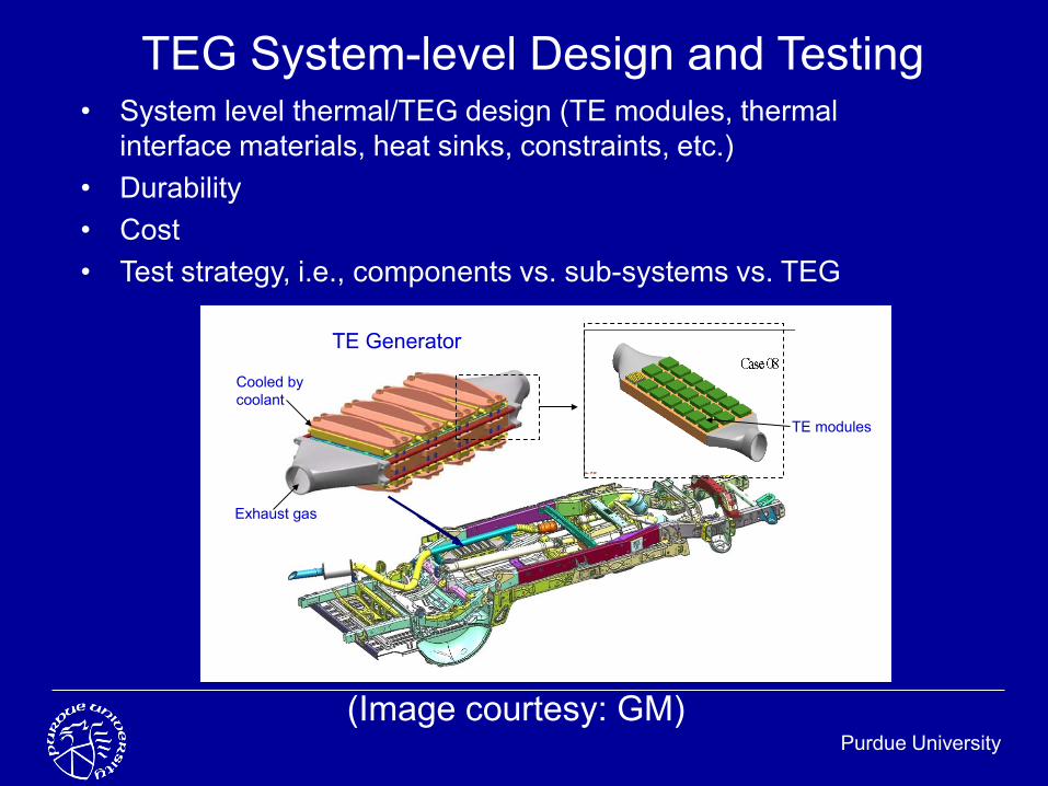
TEG System-level Design and Testing• System level thermal/TEG design (TE modules, thermal
interface materials, heat sinks, constraints, etc.)• Durability• Cost• Test strategy, i.e., components vs. sub-systems vs. TEG
TE modules
Exhaust gas
Cooled by coolant
TE Generator
(Image courtesy: GM)

Purdue University
• Project started from Jan. 1st, 2011• Purdue/GM project kick-off meeting on Dec.
13, 2010, at Purdue
Purdue University
We thank the support from:NSF, PM: Dr. Ted BergmanDOE, PM: Dr. John Fairbanks, Dr. Tom Avedisian

Purdue University

Purdue University
Purdue University
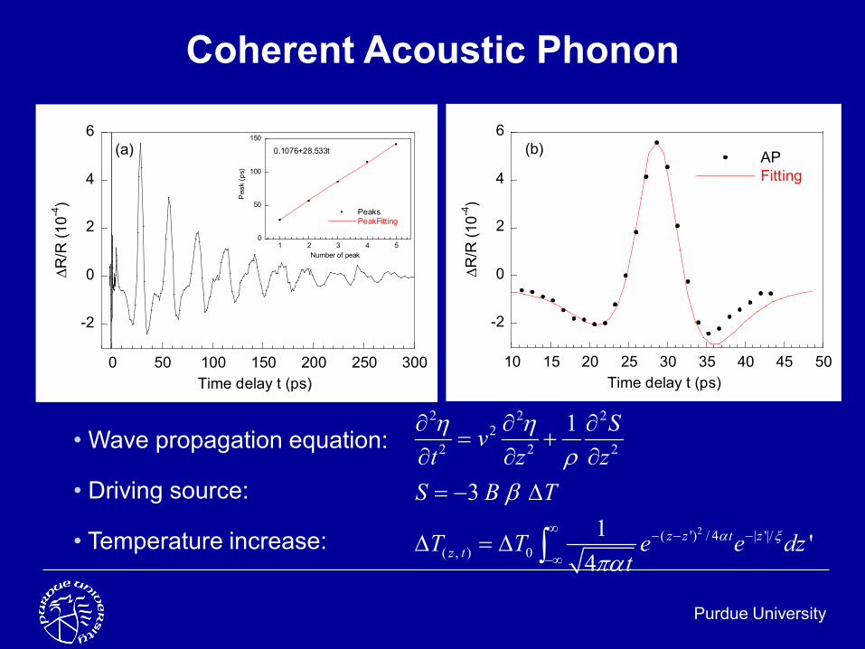
Coherent Acoustic Phonon
-2
0
2
4
6
0 50 100 150 200 250 300
∆R/R
(10-4
)
Time delay t (ps)
(a)
0
50
100
150
1 2 3 4 5
PeaksPeakFitting
Pea
k (p
s)
Number of peak
0.1076+28.533t
-2
0
2
4
6
10 15 20 25 30 35 40 45 50
APFitting
∆R/R
(10-4
)
Time delay t (ps)
(b)
2
2 2 22
2 2 2
( ') / 4 | '|/( , ) 0
1
31 '
4z z t z
z t
Svt z z
S B T
T T e e dzt
α ξ
η ηρ
β
πα∞ − − −
−∞
∂ ∂ ∂= +
∂ ∂ ∂= − ∆
∆ = ∆ ∫
• Wave propagation equation:
• Driving source:
• Temperature increase:

Purdue University
Experimental Setup for Pump-and-probe Measurements
Pump-and-probe set-upPulse shaping apparatus

Purdue University
Bi2Te3, Sb2Te3 and Bi2Te3/Sb2Te3 Superlattice
Bi2Te3 Sb2Te3 Superlattice

Purdue University
Phonon Scattering in Bi2Te3/Sb2Te3 Superlattice• Scattering of phonon is due to phonon-charge, phonon-phonon, and
phonon-boundary/interface interactions.• Scattering rate of coherent phonon increases linearly with pump
fluence.• Phonon scattering in bulk Bi2Te3, bulk Sb2Te3 and Bi2Te3/Sb2Te3
superlattice is measured and compared.
Purdue University
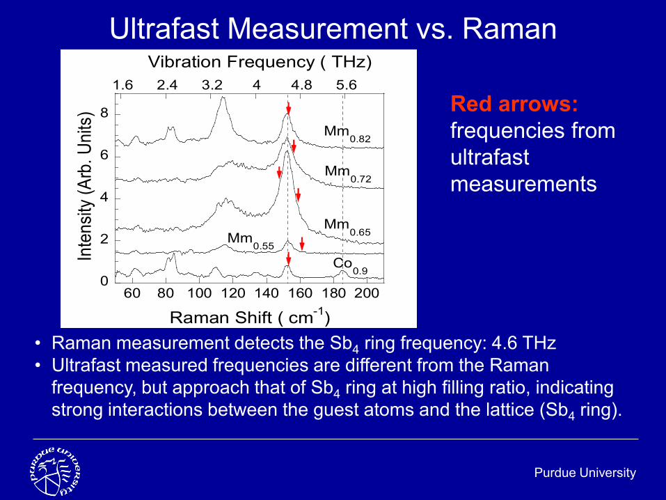
Ultrafast Measurement vs. Raman
0
2
4
6
8
60 80 100 120 140 160 180 200
1.6 2.4 3.2 4 4.8 5.6In
tens
ity (A
rb. U
nits
)
Raman Shift ( cm-1)
Mm0.82
Mm0.72
Mm0.65Mm
0.55
Co0.9
Vibration Frequency ( THz)
• Raman measurement detects the Sb4 ring frequency: 4.6 THz• Ultrafast measured frequencies are different from the Raman
frequency, but approach that of Sb4 ring at high filling ratio, indicating strong interactions between the guest atoms and the lattice (Sb4 ring).
Red arrows:frequencies from ultrafast measurements

Purdue University
ZT ~ 1 in typical bulk thermal electric materials.
A good thermoelectric material means low electric resistivity ρ and low thermal conductivity κ (phonon glass electron crystal – PGEC)
Figure of merit:
• Carnot efficiency:
• ZT = 1 corresponds to η =10% • ZT = 4 corresponds to η = 30% • Home refrigerator: η ~ 30% • Bi2Te3/Sb2Te3 Superlattice: ZT = 2.4
cold
hot cold
TT T
η =−
Rowe, Thermoelectrics Handbook: Macro to Nano, CRC Press (2006).

Purdue University
- A systematic study of the effect of phonon scattering in TE materials, and the resulting thermal conductivity reduction.
- Effect of filling ratio of misch metal in different family of skutterudites.
- A theoretical understanding on the effect of the rattling behavior of the filled elements.

![Design of a Solar Thermoelectric Generator Undergraduate ......solar thermal applications, thermoelectrics are more efficient 2]. This research proposes [to design, build, and test](https://cdn.vdocument.in/doc/165x107/5ec9e892910d163d675d4c5e/design-of-a-solar-thermoelectric-generator-undergraduate-solar-thermal-applications.jpg)


