1
Photovoltaic Devices
N. Wyrsch
EPFL – IMT - PVLab
Highlights in Microtechnology, 2014
HIM 2014 : Photovoltaic devices N. Wyrsch
Content
• Applications overviews
• Brief history
• Basics of photovoltaics (PV)
• Physical principle and performance limits
• Multi-junction devices
• PV technologies
• Si thin-film technologies
• Module technology
• Photodiodes and microsystems
2

2
Applications, History and Motivation
HIM 2014 : Photovoltaic devices N. Wyrsch
Photovoltaic effect
Edmund Becquerel, the French experimental physicist, discovered (in 1839, at the age of 19) the photovoltaic effect while experimenting (in his father’s laboratory - Antoine-César Becquerel’s laboratory) with an electrolytic cell made up of two metal electrodes placed in an electricity-conducting solution--generation increased when exposed to light.
E. Becquerel, 'On electron effects under the influence of solar radiation.' Comptes Rendus 9, 561.
4

3
HIM 2014 : Photovoltaic devices N. Wyrsch
Brief history
1839 : Discovery of photovoltaic effect by Becquerel1877 : Observation of the photovoltaic effect in solid selenium by W.G. Adams and R.E. Day1883 : Description of the first solar cells made from selenium wafers by Charles Fritts (with
efficiency < 1%)1888 : Edward Weston receives first US patent for "solar cell" 1905 : Albert Einstein’s paper on the photoelectric effect1916 : Experimental proof of Einstein’s theory on photoelectric effect by Robert Millikan1922 : Einstein wins Nobel prize for 1904 paper on photoelectric effect1941 : First silicon photovoltaic cell developed by Ohl1954 : First high-power silicon PV cell (achieving 6%) by Bell Labs.
The New York Times forecasts that solar cells will eventuallylead to a source of "limitless energy of the sun".
1958 : US Vanguard I space satellite powered by a PV array1963 : Viable photovoltaic module of silicon solar cells produced
by Sharp Japan installs a 242-watt PV array on a lighthouse, the world's largest array at that time.
1970s : PV costs driven down by 80%, allowing for applications such as offshore navigation warning lights and horns lighthouses, railroad crossings, and remote use where utility-grid connections are too costly; start of mass production.
2013 : World-wide PV production > 30 GW/year– Approx. surface : 200 km2 (1/3 of lake of Geneva surface)– Equivalent annual energy production of 4 nuclear power plants
5
HIM 2014 : Photovoltaic devices N. Wyrsch
Devices and Applications
• Solar cells
• Photodiodes– Flat panel imagers (a-Si:H)
– Particle detectors (X, a, b, g)
– Light sensors
– Position detectors
– Spatial modulators (optical valves)
– Bio-chips
– Smart windows
– …..
6

4
HIM 2014 : Photovoltaic devices N. Wyrsch
Building integration of photovoltaics
7
HIM 2014 : Photovoltaic devices N. Wyrsch
Building integration of photovoltaics
Integration with partial shadowing
8

5
HIM 2014 : Photovoltaic devices N. Wyrsch
PV fields
9
HIM 2014 : Photovoltaic devices N. Wyrsch
Solar energy potential
• Yearly solar energy irradiation on Earth 10’000 x World energy consumption
• One hour of solar irradiation on Earth surface Yearly World energy consumption
• Irradiation (sea level, full sun): 1 kWh/m2
• World primary energy consumption :– Energy: >11 GToe
– Power > 13 TW
Toe : Ton oil equivalent 10 MWh
10
6
HIM 2014 : Photovoltaic devices N. Wyrsch
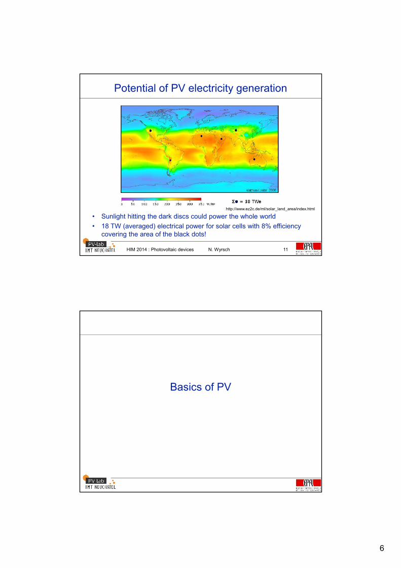
Potential of PV electricity generation
• Sunlight hitting the dark discs could power the whole world
• 18 TW (averaged) electrical power for solar cells with 8% efficiency covering the area of the black dots!
http://www.ez2c.de/ml/solar_land_area/index.html
11
Basics of PV
7
HIM 2014 : Photovoltaic devices N. Wyrsch
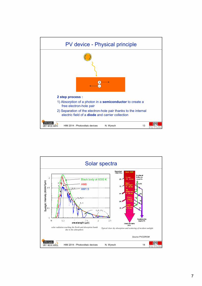
PV device - Physical principle
2 step process :
1) Absorption of a photon in a semiconductor to create a free electron-hole pair
2) Separation of the electron-hole pair thanks to the internal electric field of a diode and carrier collection
+-
13
HIM 2014 : Photovoltaic devices N. Wyrsch
Solar spectra
solar radiation reaching the Earth and absorption bands due to the atmosphere.
Typical clear sky absorption and scattering of incident sunlight.
Source PVCDROM
AM0
AM1.5
Black body at 6000 K
14

8
HIM 2014 : Photovoltaic devices N. Wyrsch
Air mass
• Air Mass : Attenuation (through the atmosphere)
where a is the angle between the sun beam and the vertical direction.– AM0: solar spectrum
(outside of the atmosphere)– AM1: solar spectrum on earth
surface when the sun is at the vertical direction
– AM1.5: angle of 45° of the sun with respect to the vertical direction.
– AMx defines both the spectrum and the radiation intensity.
– AM1.5 100 mW/cm2
– AM1.5G (Global), AM1.5D (Direct)
• Efficiencies of PV systems are usually calibrated at this intensity.
acos1AM
a
15
HIM 2014 : Photovoltaic devices N. Wyrsch
Spectral change of illumination
Daily (and seasonal) changes of spectral irradiation density
AM0: spaceAM1: equatorAM1.5 (central Europe, equinox, noon, 48° above horizon)
30° above horizon20° above horizon400 600 800 1000
0.0
0.5
1.0
1.5
2.0 AM0 (data)
AM1
AM1.5 (data)
AM2
AM3
Sp
ect
ral i
rra
dia
ton d
en
sity
[W
/m2nm
Wavelength [nm]
• Differences mostly in the visible part of the spectrum• Maximum irradiation (normal surface): 1 kW/m2
• Yearly irradiation (Switzerland): 800-1200 kWh/m2/year(dependent on the local climatic conditions)
16
9
HIM 2014 : Photovoltaic devices N. Wyrsch
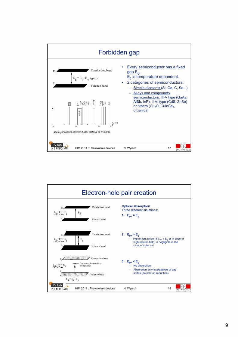
Forbidden gap
1.0 2.0 2.5
E [eV]
0
g
Ge
Si
Cu
SIn
PG
aAs
CdT
e
AlS
b
a-S
i:H
Cu
O
Se GaP
CdS
2 2
a-G
e:H
• Every semiconductor has a fixed gap Eg,Eg is temperature dependent.
• 2 categories of semiconductors:
– Simple elements (Si, Ge, C, Se...).
– Alloys and compounds semiconductors: III-V type (GaAs, AlSb, InP), II-VI type (CdS, ZnSe) or others (Cu2O, CuInSe2, organics)
Conduction band E c
Valence band
E v
E = E - E c v
( gap ) g
gap Eg of various semiconductor material at T=300 K
17
HIM 2014 : Photovoltaic devices N. Wyrsch
Electron-hole pair creation
Optical absorptionThree different situations:
1. Eph = Eg
2. Eph > Eg
- Impact ionization (if Eph » Eg or in case of high electric field) is negligible in the case of solar cell
3. Eph < Eg
– No absorption
– Absorption only in presence of gap states (defects or impurities);
Conduction band E c
Valence band E v
hv = E E ph
= g
E g
Conduction band E c
Valence band E v
hv > E E ph
= g E g
Conduction band
Valence bandEv
Ec
hv < E Eph
= Gap states due to defects or impurities
E = E - Ec v g
g
18

10
HIM 2014 : Photovoltaic devices N. Wyrsch
Absorption process
High band gap (e.g. a-Si) Low band gap (e.g. mc-Si)
Photons with energy less than the band gap are not absorbedPhoton energy in excess of band gap is lost to thermalization
-
+ +
-
19
HIM 2014 : Photovoltaic devices N. Wyrsch
Bandgaps
• Direct bandgap semiconductors:GaAs, InP, …
• High absorption coefficient
• “Non direct” bandgap:Disordered semiconductors
• Indirect bandgap semiconductors: Si, Ge, AlSb, GaP…
• Phonon must be absorbed or emitted
• Lower probability than direct excitation (without phonon interaction) lower absorption coefficient
20

11
HIM 2014 : Photovoltaic devices N. Wyrsch
Spectral conversion efficiency
Spectral conversion efficiency S
(physical limit of the conversion
efficiency)
or
where is the photon flux
Remarks:• (·q) corresponds to an electrical current
• (Eg/ q) corresponds to an electric potential
Ge
Incident photons Almost all photon are
absorbed
40% s
Si
Incident photons Une big part of the photons are
Absorbed; IR photons are not.
48% s
Incident photons
Cu2O
Une small part of the photons are absorbed
28% s
c-Ge (crystalline Germanium), Eg = 0.66 eV (small gap)
c-Si (crystalline Silicon), Eg = 1.12 eV (medium gap)
Cu2O (Cupper oxide), Eg = 2.1 eV (big gap)
timeofunitperspectrumsolartheofcontentEnergy
E g
S
timeofunitperspectrumsolartheofcontentEnergy
)q/E)(q( g
S
21
HIM 2014 : Photovoltaic devices N. Wyrsch
Spectral conversion efficiency
• S depends on
– light spectrum
– semiconductor gap
• Optimum bandgap for each spectrum
• Combination of semiconductors with different gaps may increase S
0
20
40
60
80
100
0 0.5 1 1.5 2 2.5 3
Se
a-S
i:H
GaA
s / C
dT
e
c-S
i
CIS
Ge
E [eV]g
Spe
ctra
l co
nver
sion
eff
icie
ncy
s
Incident photons
Cu2O (large Eg)
Si (small Eg)
1. High energy photons are absorbed
2. Low energy photons are absorbed
spectral conversion efficiency s as a function of gap Eg under AM1.5 illumination
Combination of 2 semiconductors with different gaps:With these 2 materials: s>60%.
22
12
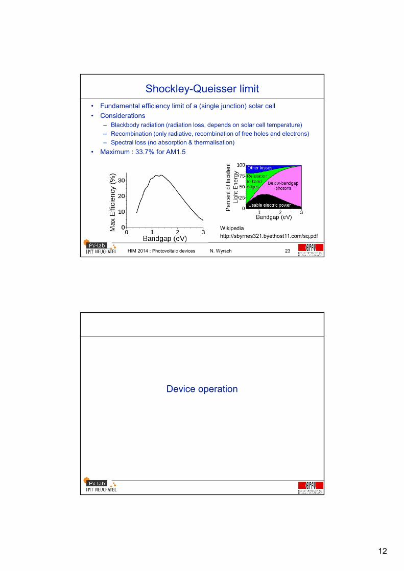
HIM 2014 : Photovoltaic devices N. Wyrsch
Shockley-Queisser limit
• Fundamental efficiency limit of a (single junction) solar cell
• Considerations
– Blackbody radiation (radiation loss, depends on solar cell temperature)
– Recombination (only radiative, recombination of free holes and electrons)
– Spectral loss (no absorption & thermalisation)
• Maximum : 33.7% for AM1.5
Wikipedia
http://sbyrnes321.byethost11.com/sq.pdf
23
Device operation

13
HIM 2014 : Photovoltaic devices N. Wyrsch
Electron-hole pair separation
• p-n diode:
– carriers’ collection by diffusion process
– crystalline solar cells
• p-i-n structure
– carriers’ collection by drift
– amorphous solar cells
– photodetectors (crystalline or amorphous)
a-Si:H p-i-n solar cell
+-
intrinsic a-Si:H
p-type a-SiC:H
n-type a-Si:H
SnO2
Glass
Al or Ag
0.3-0.5 µm
drift
a-Si:H p-i-n solar cell
+-
intrinsic a-Si:H
p-type a-SiC:H
n-type a-Si:H
SnO2
Glass
Al or Ag
0.3-0.5 µm
drift
Crystalline Si solar cell
+-
p-typesc Si
Al
p++
Ag Ag
SiO2 n+
p++ 300-500 µm
diffusion
Crystalline Si solar cell
+-
p-typesc Si
Al
p++
Ag Ag
SiO2 n+
p++ 300-500 µm
diffusion
+-
p-typesc Si
Al
+-
p-typesc Si
Al
p++
Ag Ag
SiO2 n+
p++ p++
Ag Ag
SiO2 n+
p++ 300-500 µm
diffusion
M. Zeman,Delft University
25
HIM 2014 : Photovoltaic devices N. Wyrsch
Band diagram
p
EF
p+n+
EV
EC
En
erg
y [
eV
]
0 300Depth [μm]
Crystalline Si solar cell
i
EV
EF
np
EC
Depth [nm]
En
erg
y [
eV
]
0 300
a-Si:H p-i-n solar cell
M. Zeman,Delft University
26

14
HIM 2014 : Photovoltaic devices N. Wyrsch
What is a solar cell: First approximation
In darkness:Solar cell = diode
V
I
1)exp(0
kT
qVII
Under illumination =A diode + a current source in parallel with current IL
1)exp(0
kT
qVIIIII LDL
I
IL ID
I
V
Basic equivalent circuit Ideal diode equation
I
V
-IL
I-V (current voltage) curve
Power can be delivered to a load !
V
R
27
HIM 2014 : Photovoltaic devices N. Wyrsch
Solar cell I-V curve
I
-Isc
Analyses of I-V curve
Voc V
Pmax
-Imax
-Vmax
Power
V
I
IL ID
I
IL ID
I
IL ID
Short-circuitConditionsI = -Isc, V=0
Open-circuitConditionsI=0, V = Voc,
RMPmax
Ideal power dissipation on
RM=Vmax/Imax
V
28
15
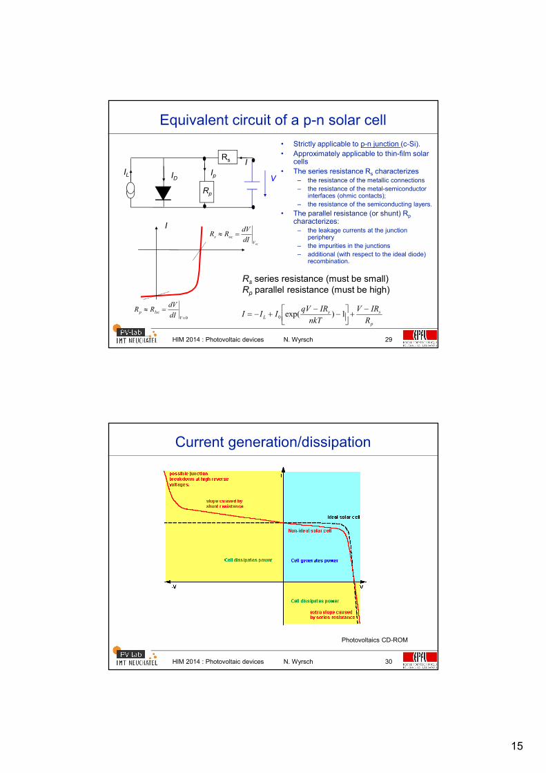
HIM 2014 : Photovoltaic devices N. Wyrsch
Equivalent circuit of a p-n solar cell
• Strictly applicable to p-n junction (c-Si).
• Approximately applicable to thin-film solar cells
• The series resistance Rs characterizes– the resistance of the metallic connections
– the resistance of the metal-semiconductor interfaces (ohmic contacts);
– the resistance of the semiconducting layers.
• The parallel resistance (or shunt) Rp
characterizes:– the leakage currents at the junction
periphery
– the impurities in the junctions
– additional (with respect to the ideal diode) recombination.
29
IL ID V
Rp
I
Ip
Rs
I
ocV
ocsdI
dVRR
0
V
IscpdI
dVRR
Rs series resistance (must be small)Rp parallel resistance (must be high)
p
ssL
R
IRV
nkT
IRqVIII
1)exp(0
HIM 2014 : Photovoltaic devices N. Wyrsch
Current generation/dissipation
Photovoltaics CD-ROM
30
16
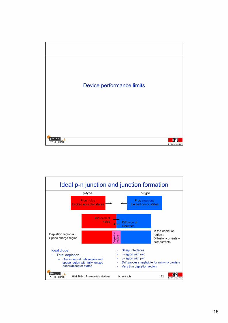
Device performance limits
HIM 2014 : Photovoltaic devices N. Wyrsch
Ideal p-n junction and junction formation
Ideal diode
• Total depletion– Quasi neutral bulk region and
space region with fully ionized donor/acceptor states
• Sharp interfaces
• n-region with n»p
• p-region with p»n
• Drift process negligible for minority carriers
• Very thin depletion region
p-type n-type
Diffusion ofelectrons
Diffusion ofholes
Deple
tion
regio
n
Free holesExcited acceptor states
Free electronsExcited donor states
Depletion region =Space charge region
In the depletion region : Diffusion currents = drift currents
32

17
HIM 2014 : Photovoltaic devices N. Wyrsch
Thermal equilibrium diagram
Depletion/space-charge region
p-bulk region n-bulk region
E
EF
x
qi
0-xp
-xn
Ei
Ev
Ec
p-type
n-type
Drift
Drift
Diffusion
Diffusion
33
In thermal equilibrium: drift current = diffusion current
HIM 2014 : Photovoltaic devices N. Wyrsch
Diode equation (Shockley)
Ideal I(V) characteristics in the dark (diffusion model)
• Solving the transport, continuity and Poisson equations (for an ideal p-n diode):
with
where
k : the Boltzmann constant q: the elementary charge
T: the absolute temperature A: the junction area
nA, nD : the dopant densities ni : intrinsic carrier density
Dp, Dn: diffusion constants of the minority carriers in the p, resp, n region
Lp , Ln: diffusion length of the minority carriers in the p, resp, n region
1exp0
Tk
qVII
B
dark
Dp
ip
An
in
nL
nqD
nL
nqDAI
22
0
34
18
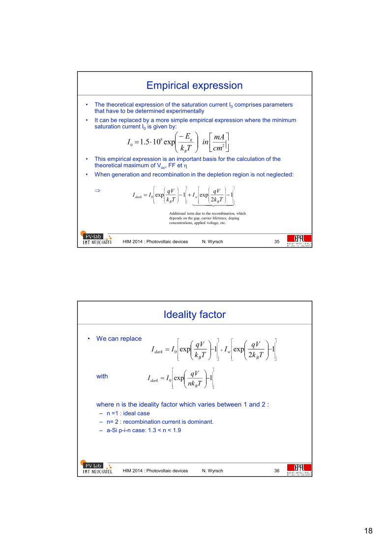
HIM 2014 : Photovoltaic devices N. Wyrsch
Empirical expression
• The theoretical expression of the saturation current I0 comprises parameters that have to be determined experimentally
• It can be replaced by a more simple empirical expression where the minimum saturation current I0 is given by:
• This empirical expression is an important basis for the calculation of the theoretical maximum of Voc, FF et
• When generation and recombination in the depletion region is not neglected:
12
exp1exp0Tk
qVI
Tk
qVII
B
w
B
dark
Additional term due to the recombination, which depends on the gap, carrier lifetimes, doping concentrations, applied voltage, etc.
2
8
0exp105.1
cm
mAin
Tk
EI
B
g
35
HIM 2014 : Photovoltaic devices N. Wyrsch
Ideality factor
• We can replace
with
where n is the ideality factor which varies between 1 and 2 :
– n =1 : ideal case
– n= 2 : recombination current is dominant.
– a-Si p-i-n case: 1.3 < n < 1.9
1exp0
Tnk
qVII
B
dark
1
2exp1exp0
Tk
qVI
Tk
qVII
B
w
B
dark
36

19
HIM 2014 : Photovoltaic devices N. Wyrsch
Superposition principle
"Superposition" principle of the
photogenerated current IL
I(V) = Idark(V) - IL
• Principle valid for a p-n diode in ideal conditions(in general not valid for thin film diodes)
I
-Isc
Voc V
Maximum power-Imax
-Vmax
IL
Dark
Illuminated
37
HIM 2014 : Photovoltaic devices N. Wyrsch
Short-circuit current Isc
• Assuming – Rs = 0 et Rp = ∞
– cell thickness sufficient for absorbing all useful light
– total collection of the carriers
– no recombination.
• Ideal illuminated diode in short-circuit condition
Isc=IL
• Theoretical maximum of Isc given by :– solar spectrum
– semiconductor gap: Isc= q, with • : number of photogenerated "electron-
hole" pairs per unit time
• q: elementary charge
• Effect of the temperature:– Isc only very weakly temperature
dependent (Eg decreases when the temperature increases).
Theoretical maximum short-circuit current under AM1.5 illumination
Experimental data
38

20
HIM 2014 : Photovoltaic devices N. Wyrsch
Open-circuit voltage Voc
• The voltage supplied by a cell directly depends on gap Eg
• From the empirical expression of the ideal p-n diode
Voc is a quasi linear function of the gap
• Limits– Eg/q is an upper bound for Voc:
– Voc increases if IL increases advantage of cells working with light concentration (higher efficiencies).
• Temperature effect– Voc decreases almost linearly when the
temperature increases (0,4% per degree Celsius for c-Si).
Voc kBT
qln
1
1, 5
IL
108mA/cm 2
Eg
q
Open-circuit voltage Voc as a function of the gap for a AM1.5 illumination with the approximations: (1)
(2)
where the values IL are obtained from the Fig. 7.26, (3) theoretical limit of Kiess [Kiess, 1995]
Voc 2
3
Eg
q
Voc kBT
qln
1
1, 5
IL
108mA/cm 2
Eg
q
q
EV
g
oc3
2
Experimental data
39
HIM 2014 : Photovoltaic devices N. Wyrsch
Fill-factor and cell power
• Fill- factor FF defined as
where Im, Vm are the current and voltage when the cell output power is maximum (maximum power point)
ocsc
mm
VI
VIFF
I
-Isc
Voc V
Maximum powerPmax=FF Isc Voc
-Imax
-Vmax
40
21
HIM 2014 : Photovoltaic devices N. Wyrsch
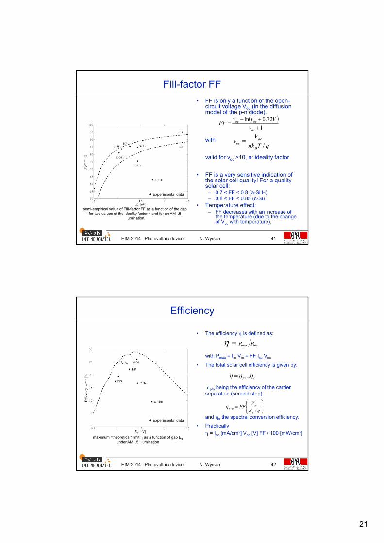
Fill-factor FF
• FF is only a function of the open-circuit voltage Voc (in the diffusion model of the p-n diode).
with
valid for voc >10, n: ideality factor
• FF is a very sensitive indication of the solar cell quality! For a quality solar cell:– 0.7 < FF < 0.8 (a-Si:H)– 0.8 < FF < 0.85 (c-Si)
• Temperature effect:– FF decreases with an increase of
the temperature (due to the change of Voc with temperature).
1
72.0ln
oc
ococ
v
VvvFF
qTnk
Vv
B
ococ
/
semi-empirical value of Fill-factor FF as a function of the gap for two values of the ideality factor n and for an AM1.5
illumination.
Experimental data
41
HIM 2014 : Photovoltaic devices N. Wyrsch
Efficiency
• The efficiency is defined as:
with Pmax = Im Vm = FF Isc Voc
• The total solar cell efficiency is given by:
p/n being the efficiency of the carrier separation (second step)
and s the spectral conversion efficiency.
• Practically
= Isc [mA/cm2] Voc [V] FF / 100 [mW/cm2]
incPPmax
snp ./
qE
VFF
g
ocnp
//
maximum "theoretical" limit as a function of gap Eg
under AM1.5 illumination
Experimental data
42
22
HIM 2014 : Photovoltaic devices N. Wyrsch
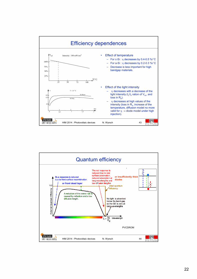
Efficiency dependences
• Effect of temperature
– For c-Si : decreases by 0.4-0.5 %/˚C
– For a-Si : decreases by 0.2-0.3 %/˚C
– Decrease is less important for high bandgap materials.
• Effect of the light intensity
– decreases with a decrease of the light intensity (IL/I0 ration of Voc, and loss in Rp).
– decreases at high values of the intensity (loss in Rs, increase of the temperature, diffusion model no more valid for diode model under high injection).
100%
50%
25%
75%
25 50 75 100
T[°C]
rel Intensity : 100 mW/cm
2
12%
6%
14%
0 0,5 1 1,5
Sun
T = 25 ° C
Si-Mono
Si-Poly
2
43
HIM 2014 : Photovoltaic devices N. Wyrsch
Quantum efficiency
PVCDROM
or front dead layer
or insufficiently thick diodes
-
+
--
++
44
23
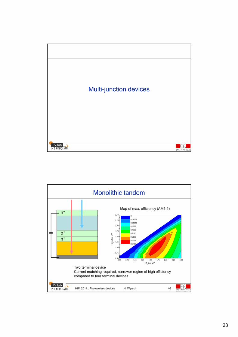
Multi-junction devices
HIM 2014 : Photovoltaic devices N. Wyrsch
n+
Monolithic tandem
p+
n+
Two terminal deviceCurrent matching required, narrower region of high efficiencycompared to four terminal devices
0,50 0,75 1,00 1,25 1,50 1,75 2,00 2,25 2,500,50
0,75
1,00
1,25
1,50
1,75
2,00
2,25
2,50
Eg top [eV]
Egbottom
[e
V]
0
0,04325
0,08650
0,1298
0,1730
0,2163
0,2595
0,3028
0,3460
Map of max. efficiency (AM1.5)
46
24
HIM 2014 : Photovoltaic devices N. Wyrsch
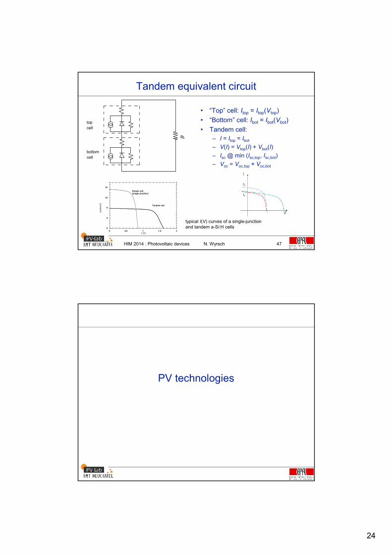
Tandem equivalent circuit
• “Top” cell: Itop = Itop(Vtop)
• “Bottom” cell: Ibot = Ibot(Vbot)
• Tandem cell:
– I = Itop = Ibot
– V(I) = Vtop(I) + Vbot(I)
– Isc @ min (Isc,top, Isc,bot)
– Voc = Voc,top + Voc,bot
top
cell
bottom
cell
RL
0
4
8
12
16
0 0.5 1 1.5 2
I [m
A/c
m2]
Simple cell (single junction)
Tandem cell
V [V]
typical I(V) curves of a single-junction and tandem a-Si:H cells
47
PV technologies

25
HIM 2014 : Photovoltaic devices N. Wyrsch
PV technologies
• Bulk technologies:
– Monocrystalline silicon
– Polycrystalline silicon
– Ribbon silicon
– GaAs (space application, concentrators), InP (space application)
• Thin-film technologies:
– Amorphous silicon
– Micro-/nano-crystalline silicon. micromorph
– CdTe (Cadmium telluride)
– CIGS (Cupper Indium Gallium Diselenide)
– CIS (Cupper Indium Diselenide, Cupper Indium Sulfide)
• Others:
– Dye cells, “Graetzel”
– Organic cells, polymers
49
HIM 2014 : Photovoltaic devices N. Wyrsch
Conversion efficiency vs. time
http://www.nrel.gov/ncpv/images/efficiency_chart.jpgCommercial cells exhibit efficiencies reduced by 20-60%
50

26
HIM 2014 : Photovoltaic devices N. Wyrsch 51
PV Development – Installed capacity (2013)
EIA PVPS Report
PV installed: > 134 GW, 2013 : +36.9 GW (fastest growth in Asia)
• World share of PV in electricity production : 0.85%
HIM 2014 : Photovoltaic devices N. Wyrsch
c-Si standard technology
Buried Contact Solar Cells Screen printed solar cells
PVCDROM
52
27
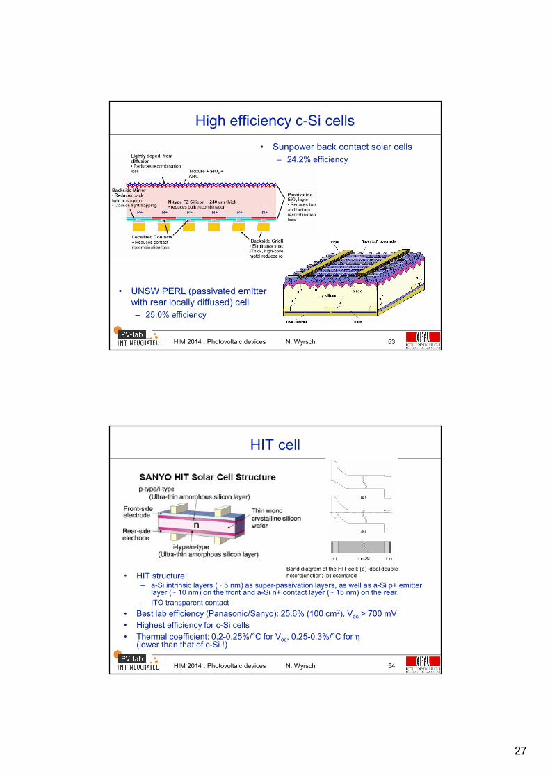
HIM 2014 : Photovoltaic devices N. Wyrsch
High efficiency c-Si cells
• UNSW PERL (passivated emitter with rear locally diffused) cell
– 25.0% efficiency
• Sunpower back contact solar cells
– 24.2% efficiency
53
HIM 2014 : Photovoltaic devices N. Wyrsch
HIT cell
• HIT structure: – a-Si intrinsic layers (~ 5 nm) as super-passivation layers, as well as a-Si p+ emitter
layer (~ 10 nm) on the front and a-Si n+ contact layer (~ 15 nm) on the rear.
– ITO transparent contact
• Best lab efficiency (Panasonic/Sanyo): 25.6% (100 cm2), Voc > 700 mV
• Highest efficiency for c-Si cells
• Thermal coefficient: 0.2-0.25%/°C for Voc, 0.25-0.3%/°C for (lower than that of c-Si !)
Band diagram of the HIT cell: (a) ideal double heterojunction; (b) estimated
54

28
Si thin-film technologies
HIM 2014 : Photovoltaic devices N. Wyrsch
Thin-film silicon characteristics
a-Si:H
• Medium gap (1.75 eV)
• Short-range order
• High hydrogen content , alloywith H (10-20%)
• Low defect density (H passivation)
• Very high resistivity, semi-isolating (>1010 cm)
• Deposited mainly by PE-CVD
• Various substrates possible
• Large area deposition
µc-Si:H (for PV applications)
• Low gap material (1.1 eV)
• few nm grain size (nano-crystalline silicon)
• Short-medium range order
• Medium hydrogen content (few %)
• Low defect density (H passivation)
• Presence of a-Si:H incubation layer, a-Si:H inter-grain tissue
• High resistivity (107-105 cm)
• Deposited mainly by PE-CVD
• Various substrates possible
• Large area deposition
56

29
HIM 2014 : Photovoltaic devices N. Wyrsch
a-Si:H optical absorption
0.5 1.0 1.5 2.0 2.5 3.0Photon energy [eV]
Absorp
tion c
oeff
icie
nt
[1/c
m]
2.48 1.24 0.83 0.62 0.50 0.41
Wavelength [micrometers]
a-SiGe:H
a-Si:H
p-type
a-SiC:H
c Si
105
104
102
101
10-1
106
103
100
Absorption coefficient
• « non-direct semiconductor »
• In visible part of spectrum 70 x higher than c-Si
• Thin film (about 1 micron) absorbs 90% of usable solar energy
Optical band gap
• Tunable
• Depends on H content
• a-Si:H based materials alloys
– C increases Eg
– Ge decreases Eg
Subbandgap defects
57
HIM 2014 : Photovoltaic devices N. Wyrsch
p-i-n solar cell
• p-i-n structure necessary for disordered semiconductors– Doped layer are very defective (dead layers)
Doped layers only serve for electric field build-up through the intrinsic layer
– The intrinsic layer is the only active layer.
• Light enters the cell through the p-layer (“window layer”)
– Minimization of hole collection path (low holemobility)
– Higher bandgap for p-layer (low optical loss)
• Electrically thin diode
High electrical field
minimal recombination in i-layer
• Optically thick diode
maximum absorption of light
Minimal thickness (processing time)
Light trapping scheme
100 Å
0.2-0.4 µm
200 Å
+
-
Glass superstrate
Transparent Conductive Oxide
p-type
Intrinsic a-Si:H
n-type
Back contact
Anti-reflection coating
58
30
HIM 2014 : Photovoltaic devices N. Wyrsch
Light trapping for thin film silicon cells
• Rough transparent conductive oxides (TCO)
• Back reflector
Back reflector
Glass
p-i-n
Front ZnO
ZnO
Tin Oxide (SnO2) deposited by AP-CVD
Roughness depends on deposition process
Zinc Oxide (ZnO) deposited by LP-CVD
Roughness depends on film thickness and temperature
59
HIM 2014 : Photovoltaic devices N. Wyrsch
Multi-junction device for higher efficiency
• Tandems
– a-Si:H / a-SiGe:H
– a-Si:H / mc-Si:H (mircomorph)
– a-Si:H / a-Si:H
• Triples
– a-SiC:H / a-Si:H / a-SiGe:H
– a-Si:H / a-SiGe:H / a-SiGe:H
– a-Si:H / mc-Si:H / mc-Si:H
– a-Si:H / a-Si:H / mc-Si:H
– a-Si:H / a-SiGe:H / mc-Si:H
– a-Si:H / mc-Si:H / mc-Ge:H
• Issues
– a-SiGe:H stability
– mc-Si:H processing
– a-SiC:H & a-SiGe:H stability
– a-SiGe:H stability
– Current matching (thick bottom)
– Current matching, very thin top
– a-SiGe:H stability
– mc-Ge:H processing
(commercially available devices in red)
60
31
HIM 2014 : Photovoltaic devices N. Wyrsch
Examples
• Micromorph Tandem devices comprising
• Introduced by IMT (EPFL)
• Advantages:– Better usage of solar spectrum
– Higher efficiency and stability
Light
Glass TCO
µc-Si:H Bottom cell
a-Si:H Top cell
Back contact
(1.1 eV gap)
(1.75 eV gap)
Light
Glass TCO
µc-Si:H Bottom cell
a-Si:H Top cell
Back contact
(1.1 eV gap)
(1.75 eV gap)
400 600 800 1000 1200 14000
0.5
1
1.5
2
2.5
Inte
nsit
y[k
W/m
2/µ
m]
Wavelength [nm]
µc-Si:H
a-Si:H
400 600 800 1000 1200 14000
0.5
1
1.5
2
2.5
Inte
nsit
y[k
W/m
2/µ
m]
Wavelength [nm]
µc-Si:H
a-Si:H
400 600 800 1000 1200 14000
0.5
1
1.5
2
2.5
400 600 800 1000 1200 1400400 600 800 1000 1200 14000
0.5
1
1.5
2
2.5
0
0.5
1
1.5
2
2.5
Inte
nsit
y[k
W/m
2/µ
m]
Wavelength [nm]
µc-Si:H
a-Si:H
61
~1.8 eV
~1.6 eV
~1.4 eV
• UniSolar monolithic triple junction, flexible modules on steel:– -stable cell efficiency: 13.1%
– -module efficiency ~8%
PV modules

32
HIM 2014 : Photovoltaic devices N. Wyrsch
Module serial connection
+ - 0.6 V 0.6 V 0.6 V 0.6 V
Bulk technologies
Monolithic interconnectionfor thin-film cells
Thin-filmtechnologies p-i-n
Metall
TCO
Substrate (glass, polymer or isolated metal)
+ -
63
HIM 2014 : Photovoltaic devices N. Wyrsch
Monolithic interconnection
Deposition of TCO on glass
Laser scribing of TCO
Deposition of a-Si diode
Laser scribing of a-Si:H diode
Deposition of back contact
Laser scribing of back contact
Testing of finished module
Dead areaActive area
64
33
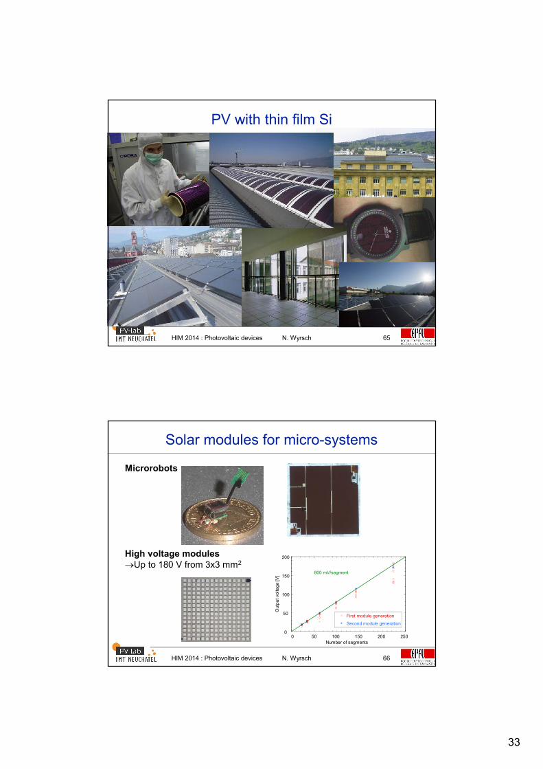
HIM 2014 : Photovoltaic devices N. Wyrsch
PV with thin film Si
65
HIM 2014 : Photovoltaic devices N. Wyrsch
Solar modules for micro-systems
0
50
100
150
200
0 50 100 150 200 250
First module generation
Second module generation
Ou
tput
voltage [V
]
Number of segments
800 mV/segment
Microrobots
High voltage modulesUp to 180 V from 3x3 mm2
66

34
a-Si photodiodes
HIM 2014 : Photovoltaic devices N. Wyrsch
Thin-film Solar cells vs Photodiodes
• Using primary photoconductivity (device with blocking contacts) given by the collection of photo-generated carriers
• Iph=Gewith : quantum efficiency, 1 (a-Si:H cells)
+
hn
A
-+
nip
Voltage
Curr
ent
densi
ty
blocking contact:
diode characteristic
Iphdark
illuminated
Operation conditions for a solar cell
Operation conditions for a photodiode
68

35
HIM 2014 : Photovoltaic devices N. Wyrsch
Fluorescence detector, microfluidic
B Optical micrograph of the top view of the integrated fluorescence detector.
A Schematic crosssectional view of a microlens and an integrated a-Si:H fluorescence detector, forming a compact platform where microfluidic CE device is mounted. Kamei, MRS 2010
69
HIM 2014 : Photovoltaic devices N. Wyrsch
Vertical Integration of Detector Arrays
• Technology known as– Thin-Film on ASIC (TFA)
– Thin-Film on CMOS (TFC)
– Above IC technology
– Elevated diode
• Benefits
– High fill-factor, high sensitivity
– No trade off between sensitivity and circuit complexity
– No dead area
CMOS circuit
Front electrode
Back electrode
Insulation layer
a-Si:H photodiode layer
70
36
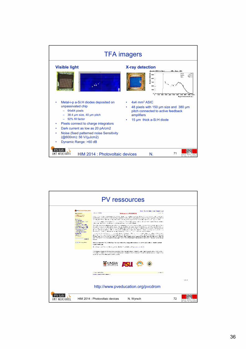
Visible light
• Metal-i-p a-Si:H diodes deposited on unpassivated chip
– 64x64 pixels
– 38.4 µm size, 40 µm pitch
– 92% fill factor
• Pixels connect to charge integrators
• Dark current as low as 20 pA/cm2
• Noise (fixed patterned noise Sensitivity (@600nm): 56 V/(µJcm2)
• Dynamic Range: >60 dB
TFA imagers
X-ray detection
• 4x4 mm2 ASIC
• 48 pixels with 150 µm size and 380 µm pitch connected to active feedback amplifiers
• 15 µm thick a-Si:H diode
HIM 2014 : Photovoltaic devices N. Wyrsch
71
HIM 2014 : Photovoltaic devices N. Wyrsch
PV ressources
http://www.pveducation.org/pvcdrom
72
37
HIM 2014 : Photovoltaic devices N. Wyrsch
Bibliography
• Books– S.M. Sze, Semiconductor Devices
– Solar Cells: Operating Principles, Technology and System Applications, M. Green, University of New South Wales
– Silicon Solar Cells: Advanced Principles and Practice, M.A. Green, University of New South Wales
– A. Shah, Thin-film silicon solar cells, EPFL Press, 2010.
– J. Kanicki, Amorphous and Microcrystalline Semiconductor Devices, 1991, Artech House
– R.A. Street, Hydrogenated Amorphous Silicon, Cambridge University Press, 1991.
– A. Ricaud, Photopiles solaires, PPUR, 1997
– A. Goetzberger, Sonnenergie: Photovoltaik, Teubner, 1997.
• Other– Photovoltaics: Devices, Systems and Applications CD-ROM by C.
Honsberg and S. Bowden, University of New South Wales,2nd edition online at : http://www.pveducation.org/pvcdrom
73


