
Cat.No.C85E-4
Safety Standard Certified Ceramic Capacitors/High Voltage Ceramic Capacitors
C85E.pdfApr.7,2014
!Note • Please read rating and !CAUTION (for storage, operating, rating, soldering, mounting and handling) in this catalog to prevent smoking and/or burning, etc.• This catalog has only typical specifi cations. Therefore, please approve our product specifi cations or transact the approval sheet for product specifi cations before ordering.

EU RoHS Compliant All the products in this catalog comply with EU RoHS. EU RoHS is "the European Directive 2011/65/EU on the Restriction of the Use
of Certain Hazardous Substances in Electrical and Electronic Equipment." For more details, please refer to our website 'Murata's Approach for EU RoHS'
(http://www.murata.com/info/rohs.html).
C85E.pdfApr.7,2014
!Note • Please read rating and !CAUTION (for storage, operating, rating, soldering, mounting and handling) in this catalog to prevent smoking and/or burning, etc.• This catalog has only typical specifi cations. Therefore, please approve our product specifi cations or transact the approval sheet for product specifi cations before ordering.
CONTENTS
Part Numbering 2
Type KY (Basic Insulation) -Class X1, Y2- (Recommend) 5
Type KH (Basic Insulation) -Class X1, Y2- 8
Type KX New Small Size (Reinforced Insulation) -Class X1, Y1- (Recommend) 10
Type KX (Reinforced Insulation) -Class X1, Y1- 13
Type KY/KH/KX Specifications and Test Methods 15
DEJ Series -Based on the Electrical Appliance and Material Safety Law of Japan- 19
DEJ Series Specifications and Test Methods 20
Safety Certified Ceramic Capacitors Characteristics Data (Typical Example) 23
Safety Certified Ceramic Capacitors Packaging 26
Safety Certified Ceramic Capacitors !Caution 28
Safety Certified Ceramic Capacitors Notice 31
DES Series (125°C Guaranteed/Low-dissipation Factor/DC500V-1kV) 32
DES Series Specifications and Test Methods 34
DEH Series (125°C Guaranteed/Low-dissipation Factor/DC500V-3.15kV) 36
DEH Series Specifications and Test Methods 39
DEA Series (125°C Guaranteed/Class 1/DC1k-3.15kV) 41
DEA Series Specifications and Test Methods 44
DEB Series (Class 2/DC1k-3.15kV) 46
DEB Series Specifications and Test Methods 49
DEC Series (Class 1, 2/DC6.3kV) 51
DEC Series Specifications and Test Methods 53
DEF Series (Only for LCD Backlight Inverter Circuit/6.3kVp-p) 55
DEF Series Specifications and Test Methods 57
High Voltage Ceramic Capacitors Characteristics Data (Typical Example) 59
High Voltage Ceramic Capacitors Packaging 60
High Voltage Ceramic Capacitors !Caution 62
High Voltage Ceramic Capacitors Notice 69
Type KJ -Class X1, Y2- (For Automotive Use/AC Line Filter of PHEV/EV Charger) 70
Type KJ Specifications and Test Methods 71
Safety Certified Ceramic Capacitors for Automotive Characteristics Data (Typical Example) 75
Safety Certified Ceramic Capacitors for Automotive Packaging 76
Safety Certified Ceramic Capacitors for Automotive !Caution 77
Safety Certified Ceramic Capacitors for Automotive Notice 80
Safety Certified Ceramic Capacitors/High Voltage Ceramic Capacitors ISO9000 Certifications 81
1
2
3
4
5
6
7
8
9
10
11
12
1
2
3
4
5
6
7
8
9
10
11
12

C85E.pdfApr.7,2014
!Note • Please read rating and !CAUTION (for storage, operating, rating, soldering, mounting and handling) in this catalog to prevent smoking and/or burning, etc.• This catalog has only typical specifi cations. Therefore, please approve our product specifi cations or transact the approval sheet for product specifi cations before ordering.
2
o Part Numbering
(Part Number)
Safety Standard Certified Ceramic Capacitors
tCapacitance
Expressed by three figures. The unit is pico-farad (pF). The first and second figures are significant digits, and the third figure expresses the number of zeros that follow the two numbers.
oIndividual Specification Code
For part number that cannot be identified without "Individual Specification," it is added at the end of part number, expressed by three-digit alphanumerics.
!0Halogen-free Compatible Product
For Electrical Appliance and Material Safety Law of Japan, the first three digits (qProduct ID and wSeries Category) express "Series Name."For Safety Certified Capacitors, the first three digits express product code. The fourth figure expresses certified type shown in rSafety Standard Certified Type column.
VerticalCrimpLong
VerticalCrimpLong
VerticalCrimpShort
Straight Long
Straight Short
VerticalCrimpTaping
Straight Taping
t
102
y
M
q
DE
u
N3
r
KY
e
E3
w
2
i
A
o
qProduct ID
wSeries Category
eTemperature Characteristics
rRated Voltage/Safety Standard Certified Type
Code
E2
KH
KY
KX
yCapacitance Tolerance
Capacitance ToleranceCode
J
K
M
Z
T5%
T10%
T20%
W80%, Y20%
ContentsOutlineCode
1
2
J
Cap. Changeor Temp. Coeff.
TemperatureRange
TemperatureCharacteristics
Rated Voltage
Code
B3
E3
F3
1X
T10%
W20%,Y55%
W30%,Y80%
W350 to Y1000ppm/D
Y25 to W85D
W20 to W85D
B
E
F
SL
Safety StandardCertified
250Vac (r.m.s.)
Class X1, Y1
Class X1, Y2
-Products based on theElectrical Appliance and
Material Safety Law of Japan-
250Vac (r.m.s.)
X1, Y2; 250Vac (r.m.s.)(Safety Standard Certified Type KH)
X1, Y2; 250Vac (r.m.s.), 300Vac (r.m.s.)(Safety Standard Certified Type KY)
X1, Y1; 250Vac (r.m.s.), 300Vac (r.m.s.)(Safety Standard Certified Type KX)
Product ID
DESafety Standard Certified Ceramic Capacitors/
High Voltage Ceramic Capacitors
uLead Style
LeadStyleCode
A2
A3
A4
A5
B2
B3
B4
B5
C3
D3
N2
N3
N4
N5
N7
P3
LeadSpacing
Pitch ofComponents
Lead Diameter
Dimensions (mm)
5
7.5
10
10
5
7.5
10
10
7.5
7.5
5
7.5
10
10
7.5
7.5
ø0.6T0.05
ø0.6W0.1,Y0.05
ø0.6T0.05
ø0.6W0.1, Y0.05
ø0.6T0.05
ø0.6T0.05
ø0.6T0.05
ø0.6W0.1, Y0.05
ø0.6T0.05
ø0.6T0.05
Y
Y
Y
Y
12.7
15
25.4
25.4
30
15
iPackaging
PackagingCode
A
B
Ammo Pack Taping
Bulk
!0
F
C85E.pdfApr.7,2014
!Note • Please read rating and !CAUTION (for storage, operating, rating, soldering, mounting and handling) in this catalog to prevent smoking and/or burning, etc.• This catalog has only typical specifi cations. Therefore, please approve our product specifi cations or transact the approval sheet for product specifi cations before ordering.
3
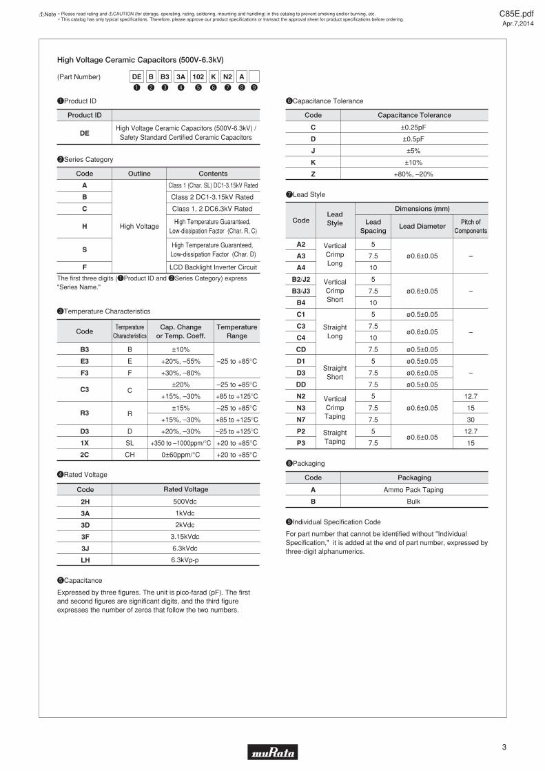
(Part Number)
High Voltage Ceramic Capacitors (500V-6.3kV)
tCapacitance
Expressed by three figures. The unit is pico-farad (pF). The first and second figures are significant digits, and the third figure expresses the number of zeros that follow the two numbers.
oIndividual Specification Code
For part number that cannot be identified without "Individual Specification," it is added at the end of part number, expressed by three-digit alphanumerics.
The first three digits (qProduct ID and wSeries Category) express "Series Name."
VerticalCrimpLong
VerticalCrimpShort
StraightLong
StraightShort
VerticalCrimpTaping
StraightTaping
t
102
y
K
q
DE
u
N2
r
3A
e
B3
w
B
i
A
o
qProduct ID
wSeries Category
eTemperature Characteristics
rRated Voltage
Code
2H
3A
3D
3F
3J
LH
yCapacitance Tolerance
Capacitance ToleranceCode
C
D
J
K
Z
±0.25pF
±0.5pF
±5%
±10%
+80%, –20%ContentsOutlineCode
A
B
C
H
S
F
Cap. Changeor Temp. Coeff.
TemperatureRange
TemperatureCharacteristics
Rated Voltage
Code
B3
E3
F3
C3
R3
D3
1X
2C
±10%
+20%, –55%
+30%, –80%
±20%
+15%, –30%
±15%
+15%, –30%
+20%, –30%
+350 to –1000ppm/°C
0±60ppm/°C
–25 to +85°C
–25 to +85°C
+85 to +125°C
–25 to +85°C
+85 to +125°C
–25 to +125°C
+20 to +85°C
+20 to +85°C
B
E
F
C
R
D
SL
CH
High Voltage
Class 1 (Char. SL) DC1-3.15kV Rated
Class 2 DC1-3.15kV Rated
Class 1, 2 DC6.3kV Rated
High Temperature Guaranteed, Low-dissipation Factor (Char. R, C)
High Temperature Guaranteed, Low-dissipation Factor (Char. D)
LCD Backlight Inverter Circuit
500Vdc
1kVdc
2kVdc
3.15kVdc
6.3kVdc
6.3kVp-p
Product ID
DEHigh Voltage Ceramic Capacitors (500V-6.3kV) /
Safety Standard Certified Ceramic Capacitors
uLead Style
LeadStyleCode
A2
A3
A4
B2/J2
B3/J3
B4
C1
C3
C4
CD
D1
D3
DD
N2
N3
N7
P2
P3
LeadSpacing
Pitch ofComponents
Lead Diameter
Dimensions (mm)
5
7.5
10
5
7.5
10
5
7.5
10
7.5
5
7.5
7.5
5
7.5
7.5
5
7.5
ø0.6±0.05
ø0.6±0.05
ø0.5±0.05
ø0.6±0.05
ø0.5±0.05
ø0.5±0.05
ø0.6±0.05
ø0.5±0.05
ø0.6±0.05
ø0.6±0.05
–
–
–
–
12.7
15
30
12.7
15
iPackaging
PackagingCode
A
B
Ammo Pack Taping
Bulk
C85E.pdfApr.7,2014
!Note • Please read rating and !CAUTION (for storage, operating, rating, soldering, mounting and handling) in this catalog to prevent smoking and/or burning, etc.• This catalog has only typical specifi cations. Therefore, please approve our product specifi cations or transact the approval sheet for product specifi cations before ordering.
4
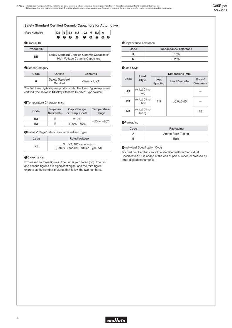
(Part Number)
Safety Standard Certified Ceramic Capacitors for Automotive
tCapacitance
Expressed by three figures. The unit is pico-farad (pF). The first and second figures are significant digits, and the third figure expresses the number of zeros that follow the two numbers.
oIndividual Specification Code
For part number that cannot be identified without "Individual Specification," it is added at the end of part number, expressed by three-digit alphanumerics.
The first three digits express product code. The fourth figure expresses certified type shown in rSafety Standard Certified Type column.
Vertical CrimpLong
Vertical CrimpShort
Vertical CrimpTaping
t
102
y
M
q
DE
u
N3
r
KJ
e
E3
w
6
i
A
o
qProduct ID
wSeries Category
eTemperature Characteristics
rRated Voltage/Safety Standard Certified Type
Code
KJ
yCapacitance Tolerance
Capacitance ToleranceCode
K
M
T10%
T20%
ContentsOutlineCode
6
Cap. Changeor Temp. Coeff.
TemperatureRange
TemperatureCharacteristics
Rated Voltage
Code
B3
E3
T10%
W20%,Y55%Y25 to W85D
B
E
Safety StandardCertified
Class X1, Y2
X1, Y2; 300Vac (r.m.s.),(Safety Standard Certified Type KJ)
Product ID
DESafety Standard Certified Ceramic Capacitors/
High Voltage Ceramic Capacitors
uLead Style
LeadStyleCode
A3
B3
N3
LeadSpacing
Pitch ofComponents
Lead Diameter
Dimensions (mm)
7.5 ø0.6T0.05
Y
Y
15
iPackaging
PackagingCode
A
B
Ammo Pack Taping
Bulk

Safety Standard Certifi ed Ceramic CapacitorsType KY (Basic Insulation) -Class X1, Y2- (Recommend)
ød
F±1.0
(in mm)
D max.
25.0
min
.
e
T max.
3.0
max
.
Lead Code Coating Extension e
A2, A3 Up to the end of crimp
ød
0.6±0.05
ød
F±0.8
D max.
e
T max.
3.0
max
.
5.0±
1.0
(in mm)
Lead Code Coating Extension e
B2, B3 Up to the end of crimp
ød
0.6±0.05
Standard No. Rated VoltageCertified No.
ULCSA
VDE
BSI
SEMKODEMKOFIMKONEMKOESTI
NSW
E379211283280
40006273
KM 37901
1207848D0100224197
P1221509412.0102
6824
250Vac (r.m.s.)
UL60384-14CSA E60384-14IEC 60384-14EN 60384-14EN 60065 (8.8, 14.2)IEC 60384-14 EN 60384-14
IEC 60384-14EN 60384-14
IEC 60384-14AS3250
CQCCQC06001017446CQC06001017447
GB/T14472
c Standard Certifi cation
Standard No. Rated VoltageCertified No.
ULCSA
VDE
BSI
SEMKODEMKOFIMKONEMKOESTI
NSW
E379211283280
40006273
KM 37901
1207848D0100224197
P1221509412.0102
6824
300Vac (r.m.s.)
UL60384-14CSA E60384-14IEC 60384-14EN 60384-14EN 60065 (8.8, 14.2)IEC 60384-14 EN 60384-14
IEC 60384-14EN 60384-14
IEC 60384-14AS3250
CQCCQC12001079706CQC12001079940
IEC 60384-14
c Features1. Compact size; diameter 25% less than Type KH.2. Operating temperature range guaranteed up to 125 degrees C.3. Dielectric strength: AC2000V (for lead spacing F=5mm) AC2600V (for lead spacing F=7.5mm)4. Class X1/Y2 capacitors certifi ed by UL/CSA/VDE/BSI/SEMKO/DEMKO/FIMKO/NEMKO/ ESTI/NSW/CQC.5. Coated with fl ame-retardant epoxy resin (conforming to UL94V-0 standard). We recommend a halogen-free product* as our standard item. * Cl=900ppm max., Br=900ppm max. and Cl+Br=1500ppm max.6. Taping available for automatic insertion.7. AC300V Rated Voltage item are newly added.
c Applications1. Ideal for use as X/Y capacitors for AC line fi lters and primary-secondary coupling on switching power supplies and AC adapters.2. Ideal for use on D-A isolation and noise absorption for DAA modems without transformers. Do not use these products in any automotive power train or safety equipment including battery chargers for electric vehicles and plug-in hybrids.Only Murata products clearly stipulated as "for Automotive use" on its catalog can be used for automobile applications such as power train and safety equipment.
C85E.pdfApr.7,2014
5
!Note • Please read rating and !CAUTION (for storage, operating, rating, soldering, mounting and handling) in this catalog to prevent smoking and/or burning, etc.• This catalog has only typical specifi cations. Therefore, please approve our product specifi cations or transact the approval sheet for product specifi cations before ordering.
1
[Bulk]Vertical Crimp Long (A2, A3)
[Bulk]Vertical Crimp Short (B2, B3)

Example Item
t Manufactured Date Code
Class Code X1Y2
Rated Voltage Mark 250~, 300~
Halogen Free Mark HF
e Capacitance Tolerance
w Nominal Capacitance(Under 100pF: Actual value, 100pF and over: 3 digit system)
q Type Designation KY
472MKY250~X1Y2 HF
80D
q
w e
rt
r Company Name Code
: Made in Taiwan : Made in Thailand8 15
c Marking
Part NumberAC RatedVoltage
Temp.Char.
CapacitanceBodyDia. D
LeadSpacing F
(mm)
BodyThickness T
LeadPackage
Long Bulk
LeadPackage
Short Bulk
LeadPackageTaping
DE21XKY100JpppM02F 250Vac(r.m.s.) SL 10pF±5% 8.0mm max. 7.5 5.0mm max. A3B B3B N3A
DE21XKY150JpppM02F 250Vac(r.m.s.) SL 15pF±5% 8.0mm max. 7.5 5.0mm max. A3B B3B N3A
DE21XKY220JpppM02F 250Vac(r.m.s.) SL 22pF±5% 8.0mm max. 7.5 5.0mm max. A3B B3B N3A
DE21XKY330JpppM02F 250Vac(r.m.s.) SL 33pF±5% 8.0mm max. 7.5 5.0mm max. A3B B3B N3A
DE21XKY470JpppM02F 250Vac(r.m.s.) SL 47pF±5% 8.0mm max. 7.5 5.0mm max. A3B B3B N3A
DE21XKY680JpppM02F 250Vac(r.m.s.) SL 68pF±5% 8.0mm max. 7.5 5.0mm max. A3B B3B N3A
DE2B3KY101KpppM02F 250Vac(r.m.s.) B 100pF±10% 7.0mm max. 7.5 5.0mm max. A3B B3B N3A
DE2B3KY151KpppM02F 250Vac(r.m.s.) B 150pF±10% 7.0mm max. 7.5 5.0mm max. A3B B3B N3A
DE2B3KY221KpppM02F 250Vac(r.m.s.) B 220pF±10% 7.0mm max. 7.5 5.0mm max. A3B B3B N3A
DE2B3KY331KpppM02F 250Vac(r.m.s.) B 330pF±10% 7.0mm max. 7.5 5.0mm max. A3B B3B N3A
DE2B3KY471KpppM02F 250Vac(r.m.s.) B 470pF±10% 7.0mm max. 7.5 5.0mm max. A3B B3B N3A
DE2B3KY681KpppM02F 250Vac(r.m.s.) B 680pF±10% 8.0mm max. 7.5 5.0mm max. A3B B3B N3A
DE2E3KY102MpppM02F 250Vac(r.m.s.) E 1000pF±20% 7.0mm max. 7.5 5.0mm max. A3B B3B N3A
DE2E3KY152MpppM02F 250Vac(r.m.s.) E 1500pF±20% 7.0mm max. 7.5 5.0mm max. A3B B3B N3A
DE2E3KY222MpppM02F 250Vac(r.m.s.) E 2200pF±20% 8.0mm max. 7.5 5.0mm max. A3B B3B N3A
DE2E3KY332MpppM02F 250Vac(r.m.s.) E 3300pF±20% 9.0mm max. 7.5 5.0mm max. A3B B3B N3A
DE2E3KY472MpppM02F 250Vac(r.m.s.) E 4700pF±20% 10.0mm max. 7.5 5.0mm max. A3B B3B N3A
DE2F3KY103MpppM02F 250Vac(r.m.s.) F 10000pF±20% 14.0mm max. 7.5 5.0mm max. A3B B3B N3A
Three blank columns are fi lled with the lead and packaging codes. Please refer to the 3 columns on the right for the appropriate code.
Individual specifi cation code "M02" expresses "simplicity marking and guarantee of dielectric strength between lead wires: AC2600V."
Murata part numbers might be changed depending on lead code or any other changes. Therefore, please specify only the type name (KY) and capacitance of products
in the parts list when it is required for applying safety standard of electric equipment.
Part NumberAC RatedVoltage
Temp.Char.
CapacitanceBodyDia. D
LeadSpacing F
(mm)
BodyThickness T
LeadPackage
Long Bulk
LeadPackage
Short Bulk
LeadPackageTaping
DE21XKY100JpppM01F 250Vac(r.m.s.) SL 10pF±5% 8.0mm max. 5.0 5.0mm max. A2B B2B N2A
DE21XKY150JpppM01F 250Vac(r.m.s.) SL 15pF±5% 8.0mm max. 5.0 5.0mm max. A2B B2B N2A
DE21XKY220JpppM01F 250Vac(r.m.s.) SL 22pF±5% 8.0mm max. 5.0 5.0mm max. A2B B2B N2A
DE21XKY330JpppM01F 250Vac(r.m.s.) SL 33pF±5% 8.0mm max. 5.0 5.0mm max. A2B B2B N2A
DE21XKY470JpppM01F 250Vac(r.m.s.) SL 47pF±5% 8.0mm max. 5.0 5.0mm max. A2B B2B N2A
DE21XKY680JpppM01F 250Vac(r.m.s.) SL 68pF±5% 8.0mm max. 5.0 5.0mm max. A2B B2B N2A
DE2B3KY101KpppM01F 250Vac(r.m.s.) B 100pF±10% 7.0mm max. 5.0 5.0mm max. A2B B2B N2A
DE2B3KY151KpppM01F 250Vac(r.m.s.) B 150pF±10% 7.0mm max. 5.0 5.0mm max. A2B B2B N2A
DE2B3KY221KpppM01F 250Vac(r.m.s.) B 220pF±10% 7.0mm max. 5.0 5.0mm max. A2B B2B N2A
DE2B3KY331KpppM01F 250Vac(r.m.s.) B 330pF±10% 7.0mm max. 5.0 5.0mm max. A2B B2B N2A
DE2B3KY471KpppM01F 250Vac(r.m.s.) B 470pF±10% 7.0mm max. 5.0 5.0mm max. A2B B2B N2A
DE2B3KY681KpppM01F 250Vac(r.m.s.) B 680pF±10% 8.0mm max. 5.0 5.0mm max. A2B B2B N2A
DE2E3KY102MpppM01F 250Vac(r.m.s.) E 1000pF±20% 7.0mm max. 5.0 5.0mm max. A2B B2B N2A
Continued on the following page.
C85E.pdfApr.7,2014
6
!Note • Please read rating and !CAUTION (for storage, operating, rating, soldering, mounting and handling) in this catalog to prevent smoking and/or burning, etc.• This catalog has only typical specifi cations. Therefore, please approve our product specifi cations or transact the approval sheet for product specifi cations before ordering.
1
o Lead Spacing F=7.5mm
o Lead Spacing F=5mm
Rated Voltage 250Vac

Continued from the preceding page.
Part NumberAC RatedVoltage
Temp.Char.
CapacitanceBodyDia. D
LeadSpacing F
(mm)
BodyThickness T
LeadPackage
Long Bulk
LeadPackage
Short Bulk
LeadPackageTaping
DE2E3KY152MpppM01F 250Vac(r.m.s.) E 1500pF±20% 7.0mm max. 5.0 5.0mm max. A2B B2B N2A
DE2E3KY222MpppM01F 250Vac(r.m.s.) E 2200pF±20% 8.0mm max. 5.0 5.0mm max. A2B B2B N2A
DE2E3KY332MpppM01F 250Vac(r.m.s.) E 3300pF±20% 9.0mm max. 5.0 5.0mm max. A2B B2B N2A
DE2E3KY472MpppM01F 250Vac(r.m.s.) E 4700pF±20% 10.0mm max. 5.0 5.0mm max. A2B B2B N2A
Three blank columns are fi lled with the lead and packaging codes. Please refer to the 3 columns on the right for the appropriate code.
Individual specifi cation code "M01" expresses "simplicity marking and guarantee of dielectric strength between lead wires: AC2000V."
Murata part numbers might be changed depending on lead code or any other changes. Therefore, please specify only the type name (KY) and capacitance of products
in the parts list when it is required for applying safety standard of electric equipment.
Part NumberAC RatedVoltage
Temp.Char.
CapacitanceBodyDia. D
LeadSpacing F
(mm)
BodyThickness T
LeadPackage
Long Bulk
LeadPackage
Short Bulk
LeadPackageTaping
DE2B3KY101KpppU02F 300Vac(r.m.s.) B 100pF±10% 7.0mm max. 7.5 5.0mm max. A3B B3B N3A
DE2B3KY151KpppU02F 300Vac(r.m.s.) B 150pF±10% 7.0mm max. 7.5 5.0mm max. A3B B3B N3A
DE2B3KY221KpppU02F 300Vac(r.m.s.) B 220pF±10% 7.0mm max. 7.5 5.0mm max. A3B B3B N3A
DE2B3KY331KpppU02F 300Vac(r.m.s.) B 330pF±10% 7.0mm max. 7.5 5.0mm max. A3B B3B N3A
DE2B3KY471KpppU02F 300Vac(r.m.s.) B 470pF±10% 7.0mm max. 7.5 5.0mm max. A3B B3B N3A
DE2B3KY681KpppU02F 300Vac(r.m.s.) B 680pF±10% 8.0mm max. 7.5 5.0mm max. A3B B3B N3A
DE2E3KY102MpppU02F 300Vac(r.m.s.) E 1000pF±20% 7.0mm max. 7.5 5.0mm max. A3B B3B N3A
DE2E3KY152MpppU02F 300Vac(r.m.s.) E 1500pF±20% 7.0mm max. 7.5 5.0mm max. A3B B3B N3A
DE2E3KY222MpppU02F 300Vac(r.m.s.) E 2200pF±20% 8.0mm max. 7.5 5.0mm max. A3B B3B N3A
DE2E3KY332MpppU02F 300Vac(r.m.s.) E 3300pF±20% 9.0mm max. 7.5 5.0mm max. A3B B3B N3A
DE2E3KY472MpppU02F 300Vac(r.m.s.) E 4700pF±20% 10.0mm max. 7.5 5.0mm max. A3B B3B N3A
DE2F3KY103MpppU02F 300Vac(r.m.s.) F 10000pF±20% 14.0mm max. 7.5 5.0mm max. A3B B3B N3A
Three blank columns are fi lled with the lead and packaging codes. Please refer to the 3 columns on the right for the appropriate code.
Individual specifi cation code "U02" expresses "simplicity marking and guarantee of dielectric strength between lead wires: AC2600V."
Murata part numbers might be changed depending on lead code or any other changes. Therefore, please specify only the type name (KY) and capacitance of products
in the parts list when it is required for applying safety standard of electric equipment.
C85E.pdfApr.7,2014
7
!Note • Please read rating and !CAUTION (for storage, operating, rating, soldering, mounting and handling) in this catalog to prevent smoking and/or burning, etc.• This catalog has only typical specifi cations. Therefore, please approve our product specifi cations or transact the approval sheet for product specifi cations before ordering.
1
o Lead Spacing F=7.5mm
Rated Voltage 300Vac

Safety Standard Certifi ed Ceramic CapacitorsType KH (Basic Insulation) -Class X1, Y2-
ød
F±1.0
(in mm)
D max.
25.0
min
.
e
T max.
3.0
max
.
Lead Code Coating Extension e
A3 Up to the end of crimp
ød
0.6±0.05
[Bulk]Vertical Crimp Long (A3)
ød
F±0.8
D max.
e
T max.
3.0
max
.
5.0±
1.0
(in mm)
Lead Code Coating Extension e
B3 Up to the end of crimp
ød
0.6±0.05
[Bulk]Vertical Crimp Short (B3)
Standard No. Rated VoltageCertified No.
ULCSA
VDE
BSI
SEMKO
DEMKOFIMKONEMKOESTI
NSW
E379211343805
40002796
KM 37901
1200285D0100624195
P1221509512.0104
6529
250Vac (r.m.s.)
UL60384-14CSA E60384-14IEC 60384-14 EN 60384-14EN 60065 (8.8, 14.2)IEC 60384-14 EN 60384-14
IEC 60384-14EN 60384-14
IEC 60384-14AS3250
c Standard Certifi cation
q Type Designation
w Nominal Capacitance(Marked with 3 figures)
e Capacitance Tolerance
r Company Name Code : Made in Taiwan : Made in Thailand
t Manufactured Date Code
UL Approval Mark
CSA Approval Mark
VDE Approval Mark
BSI Approval Mark
SEMKO Approval Mark
DEMKO Approval Mark
FIMKO Approval Mark
NEMKO Approval Mark
ESTI Approval Mark
Class Code
Rated Voltage Mark
KH
BSI
X1Y2
250~
FI
N
D
KH472MX1Y2BSI
q
w
e
r
t
8
65MJ502
250~
Example Item
FI
N
MJ502
8 15
D
c Marking
c Features1. Operating temperature range guaranteed up to 125 degrees C.2. Dielectric strength: AC2600V3. Class X1/Y2 capacitors certifi ed by UL/CSA/VDE/BSI/SEMKO/DEMKO/FIMKO/NEMKO/ ESTI/NSW.4. Coated with fl ame-retardant epoxy resin (conforming to UL94V-0 standard). Please contact us when a halogen-free product* is necessary. * Cl=900ppm max., Br=900ppm max. and Cl+Br=1500ppm max.5. Taping available for automatic insertion.
c ApplicationsIdeal for use as X/Y capacitors for AC line fi lters and primary-secondary coupling on switching power supplies and AC adapters. Do not use these products in any automotive power train or safety equipment including battery chargers for electric vehicles and plug-in hybrids.Only Murata products clearly stipulated as "for Automotive use" on its catalog can be used for automobile applications such as power train and safety equipment.
C85E.pdfApr.7,2014
8
!Note • Please read rating and !CAUTION (for storage, operating, rating, soldering, mounting and handling) in this catalog to prevent smoking and/or burning, etc.• This catalog has only typical specifi cations. Therefore, please approve our product specifi cations or transact the approval sheet for product specifi cations before ordering.
2

Part NumberAC RatedVoltage
Temp.Char.
CapacitanceBodyDia. D
LeadSpacing F
(mm)
BodyThickness T
LeadPackage
Long Bulk
LeadPackage
Short Bulk
LeadPackageTaping
DE2B3KH101Kppp 250Vac(r.m.s.) B 100pF±10% 8.0mm max. 7.5 7.0mm max. A3B B3B N3A
DE2B3KH151Kppp 250Vac(r.m.s.) B 150pF±10% 8.0mm max. 7.5 7.0mm max. A3B B3B N3A
DE2B3KH221Kppp 250Vac(r.m.s.) B 220pF±10% 8.0mm max. 7.5 7.0mm max. A3B B3B N3A
DE2B3KH331Kppp 250Vac(r.m.s.) B 330pF±10% 8.0mm max. 7.5 7.0mm max. A3B B3B N3A
DE2B3KH471Kppp 250Vac(r.m.s.) B 470pF±10% 8.0mm max. 7.5 7.0mm max. A3B B3B N3A
DE2B3KH681Kppp 250Vac(r.m.s.) B 680pF±10% 9.0mm max. 7.5 7.0mm max. A3B B3B N3A
DE2E3KH102Mppp 250Vac(r.m.s.) E 1000pF±20% 8.0mm max. 7.5 7.0mm max. A3B B3B N3A
DE2E3KH152Mppp 250Vac(r.m.s.) E 1500pF±20% 9.0mm max. 7.5 7.0mm max. A3B B3B N3A
DE2E3KH222Mppp 250Vac(r.m.s.) E 2200pF±20% 10.0mm max. 7.5 7.0mm max. A3B B3B N3A
DE2E3KH332Mppp 250Vac(r.m.s.) E 3300pF±20% 12.0mm max. 7.5 7.0mm max. A3B B3B N3A
DE2E3KH472Mppp 250Vac(r.m.s.) E 4700pF±20% 13.0mm max. 7.5 7.0mm max. A3B B3B N3A
DE2F3KH103Mppp 250Vac(r.m.s.) F 10000pF±20% 16.0mm max. 7.5 7.0mm max. A3B B3B N7A
Three blank columns are fi lled with the lead and packaging codes. Please refer to the 3 columns on the right for the appropriate code.
Murata part numbers might be changed depending on lead code or any other changes. Therefore, please specify only the type name (KH) and capacitance of products
in the parts list when it is required for applying safety standard of electric equipment.
C85E.pdfApr.7,2014
9
!Note • Please read rating and !CAUTION (for storage, operating, rating, soldering, mounting and handling) in this catalog to prevent smoking and/or burning, etc.• This catalog has only typical specifi cations. Therefore, please approve our product specifi cations or transact the approval sheet for product specifi cations before ordering.
2

Safety Standard Certifi ed Ceramic CapacitorsType KX New Small Size (Reinforced Insulation) -Class X1, Y1- (Recommend)
ød
F±1.0
(in mm)
D max.
25.0
min
.
e
T max.
3.0
max
.
Lead Code Coating Extension e
A4 Up to the end of crimp
ød
0.6±0.05
[Bulk]Vertical Crimp Long (A4)
ød
F±0.8
D max.
e
T max.
3.0
max
.
5.0±
1.0
(in mm)
Lead Code Coating Extension e
B4 Up to the end of crimp
ød
0.6±0.05
[Bulk]Vertical Crimp Short (B4)
c Features1. We design capacitors much more compact in size than current Type KX, having reduced the diameter by 20% max.2. Operating temperature range guaranteed up to 125 degrees C.3. Dielectric strength: AC4000V4. Class X1/Y1 capacitors certifi ed by UL/CSA/VDE/BSI/SEMKO/DEMKO/FIMKO/NEMKO/ ESTI/IMQ/CQC.5. Can be use with a component in appliances requiring reinforced insulation and double insulation based on UL1492, IEC60065 and IEC60950.6. Coated with fl ame-retardant epoxy resin (conforming to UL94V-0 standard). We recommend a halogen-free product* as our standard item. * Cl=900ppm max., Br=900ppm max. and Cl+Br=1500ppm max.7. Taping available for automatic insertion.8. AC300V Rated Voltage item are newly added.
c Applications1. Ideal for use as X/Y capacitors for AC line fi lters and primary-secondary coupling on switching power supplies and AC adapters.2. Ideal for use on D-A isolation and noise absorption for DAA modems without transformers. Do not use these products in any automotive power train or safety equipment including battery chargers for electric vehicles and plug-in hybrids.Only Murata products clearly stipulated as "for Automotive use" on its catalog can be used for automobile applications such as power train and safety equipment. *: Small sized Type KX differs from current Type KX in electrical characteristics, such as the voltage dependency, capacitance temperature dependency, and Dielectric strength. Therefore, before replacing current Type KX, please make a performance check by equipment. Please also refer to Notice (Rating) item 2, "Performance Check by Equipment," below.
C85E.pdfApr.7,2014
10
!Note • Please read rating and !CAUTION (for storage, operating, rating, soldering, mounting and handling) in this catalog to prevent smoking and/or burning, etc.• This catalog has only typical specifi cations. Therefore, please approve our product specifi cations or transact the approval sheet for product specifi cations before ordering.
3

Standard No. Certified No.
ULCSA
VDE
BSI
SEMKODEMKOFIMKONEMKOESTIIMQ
E379211343810
40002831
KM 37901
1200074D0100424191
P1221509612.0094V4069
UL60384-14CSA E60384-14IEC 60384-14EN 60384-14EN 60065 (8.8, 14.2)IEC 60384-14 EN 60384-14
IEC 60384-14EN 60384-14
EN 60384-14
CQCCQC02001001556CQC04001011643
GB/T14472
Example Item
t Manufactured Date Code
Class Code X1Y1
Rated Voltage Mark 250~
Halogen Free Mark HF
e Capacitance Tolerance
w Nominal Capacitance (3 digit system)
q Type Designation KX
472MKX250~X1Y1 HF
80D
q
w e
rt
r Company Name Code
: Made in Taiwan : Made in Thailand8 15
c Marking Rated Voltage (AC250V) B, E Char.
C85E.pdfApr.7,2014
11
!Note • Please read rating and !CAUTION (for storage, operating, rating, soldering, mounting and handling) in this catalog to prevent smoking and/or burning, etc.• This catalog has only typical specifi cations. Therefore, please approve our product specifi cations or transact the approval sheet for product specifi cations before ordering.
3
c Standard Certifi cation Rated Voltage (AC250V) B, E Char.
Standard No. Certified No.
ULCSA
VDE
BSI
SEMKODEMKOFIMKONEMKOESTIIMQ
E379211343810
40002831
KM 37901
1200074D0100424191
P1221509612.0094V4069
UL60384-14CSA E60384-14IEC 60384-14EN 60384-14EN 60065 (8.8, 14.2)IEC 60384-14 EN 60384-14
IEC 60384-14EN 60384-14
EN 60384-14
CQCCQC12001079735CQC12001079941
IEC 60384-14
c Standard Certifi cation Rated Voltage (AC300V) B, E Char.Example Item
t Manufactured Date Code
Class Code X1Y1
Rated Voltage Mark 300~
Halogen Free Mark HF
e Capacitance Tolerance
w Nominal Capacitance (3 digit system)
q Type Designation KX
472MKX300~X1Y1 HF
80D
q
w e
rt
r Company Name Code
: Made in Taiwan : Made in Thailand8 15
c Marking Rated Voltage (AC300V) B, E Char.
Part NumberAC RatedVoltage
Temp.Char.
CapacitanceBodyDia. D
LeadSpacing F
(mm)
BodyThickness T
LeadPackage
Long Bulk
LeadPackage
Short Bulk
LeadPackageTaping
DE1B3KX101KpppN01F 250Vac(r.m.s.) B 100pF±10% 7.0mm max. 10.0 7.0mm max. A4B B4B N4A
DE1B3KX151KpppN01F 250Vac(r.m.s.) B 150pF±10% 7.0mm max. 10.0 7.0mm max. A4B B4B N4A
DE1B3KX221KpppN01F 250Vac(r.m.s.) B 220pF±10% 8.0mm max. 10.0 7.0mm max. A4B B4B N4A
DE1B3KX331KpppN01F 250Vac(r.m.s.) B 330pF±10% 7.0mm max. 10.0 7.0mm max. A4B B4B N4A
DE1B3KX471KpppN01F 250Vac(r.m.s.) B 470pF±10% 7.0mm max. 10.0 7.0mm max. A4B B4B N4A
DE1B3KX681KpppN01F 250Vac(r.m.s.) B 680pF±10% 8.0mm max. 10.0 7.0mm max. A4B B4B N4A
DE1E3KX102MpppN01F 250Vac(r.m.s.) E 1000pF±20% 7.0mm max. 10.0 7.0mm max. A4B B4B N4A
DE1E3KX152MpppN01F 250Vac(r.m.s.) E 1500pF±20% 8.0mm max. 10.0 7.0mm max. A4B B4B N4A
DE1E3KX222MpppN01F 250Vac(r.m.s.) E 2200pF±20% 9.0mm max. 10.0 7.0mm max. A4B B4B N4A
DE1E3KX332MpppN01F 250Vac(r.m.s.) E 3300pF±20% 10.0mm max. 10.0 7.0mm max. A4B B4B N4A
DE1E3KX472MpppN01F 250Vac(r.m.s.) E 4700pF±20% 12.0mm max. 10.0 7.0mm max. A4B B4B N4A
Three blank columns are fi lled with the lead and packaging codes. Please refer to the 3 columns on the right for the appropriate code.
Murata part numbers might be changed depending on lead code or any other changes. Therefore, please specify only the type name (KX) and capacitance of products
in the parts list when it is required for applying safety standard of electric equipment.
Please contact us when less than 100pF capacitance product is necessary.
Rated Voltage 250Vac

Part NumberAC RatedVoltage
Temp.Char.
CapacitanceBodyDia. D
LeadSpacing F
(mm)
BodyThickness T
LeadPackage
Long Bulk
LeadPackage
Short Bulk
LeadPackageTaping
DE1B3KX101KpppP01F 300Vac(r.m.s.) B 100pF±10% 7.0mm max. 10.0 7.0mm max. A4B B4B N4A
DE1B3KX151KpppP01F 300Vac(r.m.s.) B 150pF±10% 7.0mm max. 10.0 7.0mm max. A4B B4B N4A
DE1B3KX221KpppP01F 300Vac(r.m.s.) B 220pF±10% 8.0mm max. 10.0 7.0mm max. A4B B4B N4A
DE1B3KX331KpppP01F 300Vac(r.m.s.) B 330pF±10% 7.0mm max. 10.0 7.0mm max. A4B B4B N4A
DE1B3KX471KpppP01F 300Vac(r.m.s.) B 470pF±10% 7.0mm max. 10.0 7.0mm max. A4B B4B N4A
DE1B3KX681KpppP01F 300Vac(r.m.s.) B 680pF±10% 8.0mm max. 10.0 7.0mm max. A4B B4B N4A
DE1E3KX102MpppP01F 300Vac(r.m.s.) E 1000pF±20% 7.0mm max. 10.0 7.0mm max. A4B B4B N4A
DE1E3KX152MpppP01F 300Vac(r.m.s.) E 1500pF±20% 8.0mm max. 10.0 7.0mm max. A4B B4B N4A
DE1E3KX222MpppP01F 300Vac(r.m.s.) E 2200pF±20% 9.0mm max. 10.0 7.0mm max. A4B B4B N4A
DE1E3KX332MpppP01F 300Vac(r.m.s.) E 3300pF±20% 10.0mm max. 10.0 7.0mm max. A4B B4B N4A
DE1E3KX472MpppP01F 300Vac(r.m.s.) E 4700pF±20% 12.0mm max. 10.0 7.0mm max. A4B B4B N4A
Three blank columns are fi lled with the lead and packaging codes. Please refer to the 3 columns on the right for the appropriate code.
Murata part numbers might be changed depending on lead code or any other changes. Therefore, please specify only the type name (KX) and capacitance of products
in the parts list when it is required for applying safety standard of electric equipment.
Rated Voltage 300Vac
C85E.pdfApr.7,2014
12
!Note • Please read rating and !CAUTION (for storage, operating, rating, soldering, mounting and handling) in this catalog to prevent smoking and/or burning, etc.• This catalog has only typical specifi cations. Therefore, please approve our product specifi cations or transact the approval sheet for product specifi cations before ordering.
3

Safety Standard Certifi ed Ceramic CapacitorsType KX (Reinforced Insulation) -Class X1, Y1-
ød
F±1.0
(in mm)
D max.
25.0
min
.
e
T max.
4.0
max
.
Lead Code Coating Extension e
A5 Up to the end of crimp
ød
0.6±0.1 0.05
[Bulk]Vertical Crimp Long (A5)
ød
F±0.8
D max.
e
T max.
4.0
max
.
5.0±
1.0
(in mm)
Lead Code Coating Extension e
B5 Up to the end of crimp
ød
0.6±0.1 0.05
[Bulk]Vertical Crimp Short (B5)
Standard No. Rated VoltageCertified No.
ULCSA
VDE
BSI
SEMKODEMKOFIMKONEMKOESTIIMQ
E379211343810
40002831
KM 37901
1200074D0100424191
P1221509612.0094V4069
250Vac (r.m.s.)
UL60384-14CSA E60384-14IEC 60384-14EN 60384-14EN 60065 (8.8, 14.2)IEC 60384-14EN 60384-14
IEC 60384-14EN 60384-14
EN 60384-14
c Standard Certifi cation
FI
N
D
FI
N
D
KX222MX1Y1BSI
q
w
e
r
t
865
MJ502
250~
Example Item
MJ502
q Type Designationw Nominal Capacitance
(Under 100pF: Actual value, 100pF and over: Marked with 3 figures)e Capacitance Tolerancer Company Name Code
: Made in Taiwan : Made in Thailandt Manufactured Date Code
UL Approval MarkCSA Approval MarkVDE Approval MarkBSI Approval Mark SEMKO Approval MarkDEMKO Approval MarkFIMKO Approval MarkNEMKO Approval MarkESTI Approval MarkIMQ Approval MarkClass CodeRated Voltage Mark
KX
BSI
X1Y1250~
8 15
c Marking
c Features1. Operating temperature range guaranteed up to 125 degrees C.2. Dielectric strength: AC4000V3. Class X1/Y1 capacitors certifi ed by UL/CSA/VDE/BSI/SEMKO/DEMKO/FIMKO/NEMKO/ ESTI/IMQ.4. Can be use with a component in appliances requiring reinforced insulation and double insulation based on UL1492, IEC60065 and IEC60950.5. Coated with fl ame-retardant epoxy resin (conforming to UL94V-0 standard). Please contact us when a halogen-free product* is necessary. * Cl=900ppm max., Br=900ppm max. and Cl+Br=1500ppm max.6. Taping available for automatic insertion.
c ApplicationsIdeal for use as X/Y capacitors for AC line fi lters and primary-secondary coupling on switching power supplies and AC adapters. Do not use these products in any automotive power train or safety equipment including battery chargers for electric vehicles and plug-in hybrids.Only Murata products clearly stipulated as "for Automotive use" on its catalog can be used for automobile applications such as power train and safety equipment.
C85E.pdfApr.7,2014
13
!Note • Please read rating and !CAUTION (for storage, operating, rating, soldering, mounting and handling) in this catalog to prevent smoking and/or burning, etc.• This catalog has only typical specifi cations. Therefore, please approve our product specifi cations or transact the approval sheet for product specifi cations before ordering.
4

Part NumberAC RatedVoltage
Temp.Char.
CapacitanceBodyDia. D
LeadSpacing F
(mm)
BodyThickness T
LeadPackage
Long Bulk
LeadPackage
Short Bulk
LeadPackageTaping
DE1B3KX101Kppp 250Vac(r.m.s.) B 100pF±10% 9.0mm max. 10.0 8.0mm max. A5B B5B N5A
DE1B3KX151Kppp 250Vac(r.m.s.) B 150pF±10% 9.0mm max. 10.0 8.0mm max. A5B B5B N5A
DE1B3KX221Kppp 250Vac(r.m.s.) B 220pF±10% 9.0mm max. 10.0 8.0mm max. A5B B5B N5A
DE1B3KX331Kppp 250Vac(r.m.s.) B 330pF±10% 9.0mm max. 10.0 8.0mm max. A5B B5B N5A
DE1B3KX471Kppp 250Vac(r.m.s.) B 470pF±10% 9.0mm max. 10.0 8.0mm max. A5B B5B N5A
DE1B3KX681Kppp 250Vac(r.m.s.) B 680pF±10% 10.0mm max. 10.0 8.0mm max. A5B B5B N5A
DE1E3KX102MpppA01 250Vac(r.m.s.) E 1000pF±20% 8.0mm max. 10.0 8.0mm max. A5B B5B N5A
DE1E3KX152MpppA01 250Vac(r.m.s.) E 1500pF±20% 9.0mm max. 10.0 8.0mm max. A5B B5B N5A
DE1E3KX222MpppA01 250Vac(r.m.s.) E 2200pF±20% 10.0mm max. 10.0 8.0mm max. A5B B5B N5A
DE1E3KX332MpppA01 250Vac(r.m.s.) E 3300pF±20% 12.0mm max. 10.0 8.0mm max. A5B B5B N5A
DE1E3KX392MpppA01 250Vac(r.m.s.) E 3900pF±20% 13.0mm max. 10.0 8.0mm max. A5B B5B N5A
DE1E3KX472MpppA01 250Vac(r.m.s.) E 4700pF±20% 15.0mm max. 10.0 8.0mm max. A5B B5B N5A
Three blank columns are fi lled with the lead and packaging codes. Please refer to the 3 columns on the right for the appropriate code.
Murata part numbers might be changed depending on lead code or any other changes. Therefore, please specify only the type name (KX) and capacitance of products
in the parts list when it is required for applying safety standard of electric equipment.
C85E.pdfApr.7,2014
14
!Note • Please read rating and !CAUTION (for storage, operating, rating, soldering, mounting and handling) in this catalog to prevent smoking and/or burning, etc.• This catalog has only typical specifi cations. Therefore, please approve our product specifi cations or transact the approval sheet for product specifi cations before ordering.
4

Type KY/KH/KX Specifi cations and Test Methods
Continued on the following page.
Char. SpecificationsD.F.V2.5%D.F.V5.0%
QU400+20C*1(CF30pF)QU1000 (CU30pF)
B, EF
SL
Char. Capacitance ChangeWithin ±10%
Within +20 –55% Within +30 –80%
BEF
Char. Temperature Coefficient+350 to -1000ppm/°CSL
Type Test VoltageAC2600V(r.m.s.)AC2600V(r.m.s.)AC4000V(r.m.s.)
KYKHKX
Step Temperature (ºC)20±2-25±220±285±220±2
12345
Type Test VoltageFor lead spacing F=5mm AC2000V(r.m.s.)
For lead spacing F=7.5mm AC2600V(r.m.s.)AC2600V(r.m.s.)AC4000V(r.m.s.)
KY
KHKX
*1 "C" expresses nominal capacitance value (pF).
The lead wire of a capacitor should be dipped into molten solder for 2±0.5 sec.The depth of immersion is up to about 1.5 to 2.0mm from the root of lead wires.Temp. of solder: Lead Free Solder (Sn-3Ag-0.5Cu) 245±5°C H63 Eutectic Solder 235±5°C
8 Solderability of LeadsLead wire should be soldered with uniform coating on the axial direction over 3/4 of the circumferential direction.
The capacitance measurement should be made at each step specified in Table 3.
<Table 3>
7 Temperature Characteristics (Temp. range: -25 to +85°C)
(Temp. range: +20 to +85°C)
The capacitor should not be damaged when the test voltages from Table 1 are applied between the lead wires for 60 sec.
<Table 1>
6Dielectric Strength
Between Lead Wires
No failure
BodyInsulation
No failure
First, the terminals of the capacitor should be connected together. Then, as shown in the figure at right, a metal foil should be closely wrapped around the body of the capacitor to the distance of about 3 to 6mm from each terminal.Then, the capacitor should be inserted into a container filled with metal balls of about 1mm diameter. Finally, AC voltage from Table 2 is applied for 60 sec. between the capacitor lead wires and metal balls.
<Table 2>
The insulation resistance should be measured with DC500±50V within 60±5 sec. of charging.The voltage should be applied to the capacitor through a resistor of 1MΩ.
5 Insulation Resistance (I.R.) 10000MΩ min.
4Dissipation Factor (D.F.)Q
The capacitance, dissipation factor and Q should be measured at 20˚C with 1±0.1kHz (char. SL: 1±0.1MHz) and AC5V(r.m.s.) max.
3 Capacitance Within specified tolerance
The capacitor should be visually inspected.2 Marking To be easily legible
The capacitor should be visually inspected for evidence of defect.Dimensions should be measured with slide calipers.
1 Appearance and DimensionsNo visible defect, and dimensions are within specified range.
No. Test MethodSpecificationsItem
Operating Temperature Range: -40 to +125°C (Except for UL/VDE, -25 to +125°C)
MetalFoil about
3 to 6mm
MetalBalls
C85E.pdfApr.7,2014
15
!Note • Please read rating and !CAUTION (for storage, operating, rating, soldering, mounting and handling) in this catalog to prevent smoking and/or burning, etc.• This catalog has only typical specifi cations. Therefore, please approve our product specifi cations or transact the approval sheet for product specifi cations before ordering.

Type KY/KH/KX Specifi cations and Test Methods
Continued from the preceding page.
Continued on the following page.
Apply the rated voltage for 500±12 hrs. at 40±2°C in 90 to 95% relative humidity.Post-treatment:
Capacitor should be stored for 1 to 2 hrs. at room condition.*2
13HumidityLoading
Appearance No marked defect
I.R. 3000MΩ min.
D.F.Q
CapacitanceChange
DielectricStrength
Per Item 6
Set the capacitor for 500±12 hrs. at 40±2°C in 90 to 95% relative humidity.Post-treatment:
Capacitor should be stored for 1 to 2 hrs. at room condition.*2
12
Humidity(Under Steady State)
Appearance No marked defect
I.R. 3000MΩ min.
D.F.Q
CapacitanceChange
DielectricStrength
Per Item 6
The capacitor should be firmly soldered to the supporting lead wire and vibrated at a frequency range of 10 to 55Hz, 1.5mm in total amplitude, with about a 1-minute rate of vibration change from 10Hz to 55Hz and back to 10Hz.Apply for a total of 6 hrs., 2 hrs. each in 3 mutually perpendicular directions.
11Vibration Resistance
Appearance No marked defect
Capacitance Within the specified tolerance
D.F.Q
First the capacitor should be stored at 120+0/-5°C for 60+0/-5 sec. Then, as in the figure, the lead wires should be immersed in solder of 260+0/-5°C up to 1.5 to 2.0mm from the root of terminal for 7.5+0/-1 sec.Pre-treatment:
Capacitor should be stored at 85±2°C for 1 hr., then placed at room condition*2 for 24±2 hrs. before initial measurements.
Post-treatment:Capacitor should be stored for 1 to 2 hrs. at room condition.*2
10Soldering Effect(On-Preheat)
Appearance No marked defect
I.R. 1000MΩ min.
CapacitanceChange
Within ±10%
DielectricStrength
Per Item 6
As shown in the figure, the lead wires should be immersed in solder of 350±10°C or 260±5°C up to 1.5 to 2.0mm from the root of terminal for 3.5±0.5 sec. (10±1 sec. for 260±5°C).Pre-treatment:
Capacitor should be stored at 85±2°C for 1 hr., then placed at room condition*2 for 24±2 hrs. before initial measurements.
Post-treatment:Capacitor should be stored for 1 to 2 hrs. at room condition.*2
9Soldering Effect(Non-Preheat)
Appearance No marked defect
I.R. 1000MΩ min.
CapacitanceChange
Within ±10%
DielectricStrength
Per Item 6
Char. SpecificationsD.F.V2.5%D.F.V5.0%
QU400+20C*1(CF30pF)QU1000 (CU30pF)
B, EF
SL
Char. Capacitance ChangeWithin ±10%Within ±15%Within ± 5%
BE, FSL
Char. Capacitance ChangeWithin ±10%Within ±15%Within ± 5%
BE, FSL
Char. SpecificationsD.F.V5.0%D.F.V7.5%
QU275+5/2C*1(CF30pF)QU350 (CU30pF)
B, EF
SL
Char. SpecificationsD.F.V5.0%D.F.V7.5%
QU275+5/2C*1(CF30pF)QU350 (CU30pF)
B, EF
SL
*1 "C" expresses nominal capacitance value (pF).*2 "Room condition" Temperature: 15 to 35°C, Relative humidity: 45 to 75%, Atmospheric pressure: 86 to 106kPa
No. Test MethodSpecificationsItem
ThermalScreen
Capacitor
1.5to 2.0mm
MoltenSolder
ThermalScreen
Capacitor
1.5to 2.0mm
MoltenSolder
C85E.pdfApr.7,2014
16
!Note • Please read rating and !CAUTION (for storage, operating, rating, soldering, mounting and handling) in this catalog to prevent smoking and/or burning, etc.• This catalog has only typical specifi cations. Therefore, please approve our product specifi cations or transact the approval sheet for product specifi cations before ordering.

Type KY/KH/KX Specifi cations and Test Methods
Continued from the preceding page.
Applied Voltage170% of Rated Voltage except that once each hour the voltage is increased to AC1000V(r.m.s.) for 0.1 sec.
Continued on the following page.
*2 "Room condition" Temperature: 15 to 35°C, Relative humidity: 45 to 75%, Atmospheric pressure: 86 to 106kPa
The capacitor should be individually wrapped in at least one but not more than two complete layers of cheesecloth. The capacitor should be subjected to 20 discharges. The interval between successive discharges should be 5 sec. The UAC should be maintained for 2 min. after the last discharge.
C1,2 : 1μF±10% C3 : 0.033μF±5% 10kVL1 to 4 : 1.5mH±20% 16A Rod core chokeCt : 3μF±5% 10kV R : 100Ω±2%Cx : Capacitor under test UAC : UR±5%F : Fuse, Rated 10A UR : Rated Voltage Ut : Voltage applied to Ct
16 Active Flammability The cheesecloth should not be on fire.
As shown in the figure at right, fix the body of the capacitor and apply a tensile weight gradually to each lead wire in the radial direction of the capacitor up to 10N and keep it for 10±1 sec.15
Robustness of Terminations
Tensile
Lead wire should not be cut off. Capacitor should not be broken.
Bending
Each lead wire should be subjected to 5N of weight and bent 90° at the point of egress, in one direction, then returned to its original position and bent 90° in the opposite direction at the rate of one bend in 2 to 3 sec.
Impulse VoltageEach individual capacitor should be subjected to a 5kV (Type KX: 8kV) impulses for three times. Then the capacitors are applied to life test.
Front time (T1) =1.2μs=1.67TTime to half-value (T2) =50μs
Apply a voltage from Table 4 for 1000 hrs. at 125+2/-0°C, and relative humidity of 50% max.
<Table 4>
Post-treatment:Capacitor should be stored for 1 to 2 hrs. at room condition.*2
14 Life
Appearance No marked defect
I.R. 3000MΩ min.
CapacitanceChange
Within ±20%
DielectricStrength
Per Item 6
No. Test MethodSpecificationsItem
Ux
5kV
time
W
300
T
50
90100 (%)
t
T2
T1
UtCtCxC3C2
L1
L3
L2 R
L4
C1
S2Tr
S1
UAC
F
Oscilloscope
C85E.pdfApr.7,2014
17
!Note • Please read rating and !CAUTION (for storage, operating, rating, soldering, mounting and handling) in this catalog to prevent smoking and/or burning, etc.• This catalog has only typical specifi cations. Therefore, please approve our product specifi cations or transact the approval sheet for product specifi cations before ordering.

Type KY/KH/KX Specifi cations and Test Methods
Continued from the preceding page.
Char. Capacitance ChangeWithin ±10%Within ±20%Within ± 5%
BE, FSL
Char. SpecificationsD.F.V5.0%D.F.V7.5%
QU275+5/2C*1(CF30pF)QU350 (CU30pF)
B, EF
SL
Step Temperature (ºC)-40+0/-3
Room temp.125+3/-0
Room temp.
Time (min)303
303
1234
Step Temperature (ºC)
65+5/-0
0±3
Time(min)
15
15
Immersion WaterCleanwaterSalt
water
1
2
*1 "C" expresses nominal capacitance value (pF).*2 "Room condition" Temperature: 15 to 35°C, Relative humidity: 45 to 75%, Atmospheric pressure: 86 to 106kPa
The capacitor should be subjected to 5 temperature cycles, then consecutively to 2 immersion cycles.
<Temperature Cycle>
Cycle time: 5 cycles
<Immersion Cycle>
Cycle time: 2 cycles
Pre-treatment: Capacitor should be stored at 85±2˚C for 1 hr., then placed at room condition*2 for 24±2 hrs.
Post-treatment: Capacitor should be stored for 24±2 hrs. at room condition.*2
18
TemperatureandImmersionCycle
Appearance No marked defect
I.R. 3000MΩ min.
D.F.Q
CapacitanceChange
DielectricStrength
Per Item 6
The capacitor under test should be held in the flame in the position that best promotes burning. Each specimen should only be exposed once to the flame. Time of exposure to flame: 30 sec.
Length of flame : 12±1mmGas burner : Length 35mm min. Inside Dia. 0.5±0.1mm Outside Dia. 0.9mm max.Gas : Butane gas Purity 95% min.
17 Passive FlammabilityThe burning time should not exceed 30 sec.The tissue paper should not ignite.
No. Test MethodSpecificationsItem
Abo
ut 8
mm
200T
5mm
Test Specimen
TissueAbout 10mm Thick Board
45°
C85E.pdfApr.7,2014
18
!Note • Please read rating and !CAUTION (for storage, operating, rating, soldering, mounting and handling) in this catalog to prevent smoking and/or burning, etc.• This catalog has only typical specifi cations. Therefore, please approve our product specifi cations or transact the approval sheet for product specifi cations before ordering.

AC250V Ceramic Capacitor Non Safety Certifi ed TypeDEJ Series Based on the Electrical Appliance and Material Safety Law of Japan
c Features1. This type is based on the electrical appliance and material safety law of Japan (separated table 4).2. Coated with fl ame-retardant epoxy resin (conforming to UL94V-0 standard). Please contact us when a halogen-free product* is necessary. * Cl=900ppm max., Br=900ppm max. and Cl+Br=1500ppm max.3. Taping available for automatic insertion.
c ApplicationsIdeal for use on AC line fi lters and primary-secondary coupling for switching power supplies and AC adapters. Do not use these products in any automotive power train or safety equipment including battery chargers for electric vehicles and plug-in hybrids.Only Murata products clearly stipulated as "for Automotive use" on its catalog can be used for automobile applications such as power train and safety equipment.
Lead Code Coating Extension e
A3
C3
Up to the end of crimp
3.0 max.
(in mm)
ø d
0.6±0.05
0.6±0.05
Style
Fig. 1
Fig. 2
D max. T max.T max.
<Fig. 1> <Fig. 2>
3.0
max
.
25.0
min
.
e
ø d
25.0
min
.
F±1.0
[Bulk]Vertical Crimp Long (A3)
Straight Long (C3)
D max. T max.T max.
<Fig. 1> <Fig. 2>
3.0
max
.
5.0±
1.0
F±0.8
e
ø d 5.0±
1.0
Lead Code Coating Extension e
B3
D3
Up to the end of crimp
3.0 max.
(in mm)
ø d
0.6±0.05
0.6±0.05
Style
Fig. 1
Fig. 2
[Bulk]Vertical Crimp Short (B3)
Straight Short (D3)
C85E.pdfApr.7,2014
19
!Note • Please read rating and !CAUTION (for storage, operating, rating, soldering, mounting and handling) in this catalog to prevent smoking and/or burning, etc.• This catalog has only typical specifi cations. Therefore, please approve our product specifi cations or transact the approval sheet for product specifi cations before ordering.
5
Temp. Char.
No
min
alB
od
y D
iam
eter
Manufactured Date Code Abbreviation
E, F
Manufacturer'sIdentification
Rated Voltage Marked with code
Capacitance Tolerance Marked with code
Nominal Capacitance
ø9-11mm
ø7-8mm
Marked with 3 figures
102Z250~
16
Marked with (omitted for nominal body diameter ø8mm and under)
332Z250~ 16
c Marking
Part NumberAC RatedVoltage
Temp.Char.
CapacitanceBodyDia. D
LeadSpacing F
(mm)
BodyThickness T
LeadPackage
Long Bulk
LeadPackage
Short Bulk
LeadPackageTaping (1)
LeadPackageTaping (2)
DEJE3E2102Zppp 250Vac(r.m.s.) E 1000pF+80/-20% 7.0mm max. 7.5 4.0mm max. C3B D3B N2A P3A
DEJE3E2222Zppp 250Vac(r.m.s.) E 2200pF+80/-20% 8.0mm max. 7.5 4.0mm max. A3B B3B N2A N3A
DEJE3E2332Zppp 250Vac(r.m.s.) E 3300pF+80/-20% 9.0mm max. 7.5 4.0mm max. A3B B3B N2A N3A
DEJE3E2472Zppp 250Vac(r.m.s.) E 4700pF+80/-20% 11.0mm max. 7.5 4.0mm max. A3B B3B N2A N3A
DEJF3E2472Zppp 250Vac(r.m.s.) F 4700pF+80/-20% 8.0mm max. 7.5 4.0mm max. A3B B3B N2A N3A
DEJF3E2103Zppp 250Vac(r.m.s.) F 10000pF+80/-20% 11.0mm max. 7.5 4.0mm max. A3B B3B N2A N3A
Three blank columns are fi lled with the lead and packaging codes. Please refer to the 3 columns on the right for the appropriate code.
Taping (1): Lead spacing F=5.0mm, Taping (2): Lead spacing F=7.5mm.

DEJ Series Specifi cations and Test Methods
Char. SpecificationsD.F.V2.5%D.F.V5.0%
EF
Char. Capacitance Change Within +20
–55% Within +30
–80%EF
Step Temperature (ºC)20±2-25±220±285±220±2
12345
CdVs
0.001μFDC10kV
Continued on the following page.
The lead wire of a capacitor should be dipped into molten solder for 2±0.5 sec.The depth of immersion is up to about 1.5 to 2.0mm from the root of lead wires.Temp. of solder: Lead Free Solder (Sn-3Ag-0.5Cu) 245±5°C H63 Eutectic Solder 235±5°C
9 Solderability of LeadsLead wire should be soldered with uniform coating on the axial direction over 3/4 of the circumferential direction.
As in Figure 1, discharge is made 50 times at 5 sec. intervals from the capacitor (Cd) charged at DC voltage of specified.
Fig.1
Ct: Capacitor under test R2: 100MΩS: High-voltage switch R3: Surge resistanceR1: 1000Ω
8Discharge Test
Appearance No marked defect
I.R. 1000MΩ min.
DielectricStrength
Per Item 6
The capacitance measurement should be made at each step specified in Table 1.
<Table 1>
7 Temperature Characteristics
The capacitor should not be damaged when AC1500V(r.m.s.) are applied between the lead wires for 60 sec.
6Dielectric Strength
Between Lead Wires
No failure
BodyInsulation
No failure
First, the terminals of the capacitor should be connected together. Then, as shown in the figure at right, the capacitor should be immersed into 10% salt solution up to a position of about 3 to 4mm apart from the terminals.Finally, AC1500V(r.m.s.) is applied for 60 sec. between the capacitor lead wires and electrode plate.
The insulation resistance should be measured with DC500±50V within 60±5 sec. of charging.
5 Insulation Resistance (I.R.) 10000MΩ min.
The dissipation factor should be measured at 20°C with 1±0.1kHz and AC5V(r.m.s.) max.
4Dissipation Factor(D.F.)
The capacitance should be measured at 20°C with 1±0.1kHz and AC5V(r.m.s.) max.
3 Capacitance Within specified tolerance
The capacitor should be visually inspected.2 Marking To be easily legible
The capacitor should be visually inspected for evidence of defect.Dimensions should be measured with slide calipers.
1 Appearance and DimensionsNo visible defect, and dimensions are within specified range.
No. Test MethodSpecificationsItem
Operating Temperature Range: -25 to +85°C
Vs
R3 R1
R2
S
CdCt
About3 to 4mm
ElectrodePlate
10% Salt Solution
C85E.pdfApr.7,2014
20
!Note • Please read rating and !CAUTION (for storage, operating, rating, soldering, mounting and handling) in this catalog to prevent smoking and/or burning, etc.• This catalog has only typical specifi cations. Therefore, please approve our product specifi cations or transact the approval sheet for product specifi cations before ordering.
5

DEJ Series Specifi cations and Test Methods
Continued from the preceding page.
Char. SpecificationsD.F.V5.0%D.F.V7.5%
EF
Char. Capacitance ChangeWithin ±20%Within ±30%
EF
Continued on the following page.
*1 "Room condition" Temperature: 15 to 35°C, Relative humidity: 45 to 75%, Atmospheric pressure: 86 to 106kPa
The capacitor should be subjected to 40±2°C, relative humidity of 90 to 98% for 8 hrs., and then removed in room temperature for 16 hrs. until 5 cycles are completed.Pre-treatment:
Capacitor should be stored at 85±2°C for 1 hr., then placed at room condition*1 for 24±2 hrs. before initial measurements.
Post-treatment: Capacitor should be stored for 1 to 2 hrs. at room condition.*1
15HumidityInsulation
Appearance No marked defect
I.R. 1000MΩ min.
D.F.
CapacitanceChange
DielectricStrength
Per Item 6
Char. SpecificationsD.F.V5.0%D.F.V7.5%
EF
Char. Capacitance ChangeWithin ±20%Within ±30%
EF
Char. SpecificationsD.F.V2.5%D.F.V5.0%
EF
Set the capacitor for 500±12 hrs. at 40±2°C in 90 to 95% relative humidity.Pre-treatment:
Capacitor should be stored at 85±2°C for 1 hr., then placed at room condition*1 for 24±2 hrs. before initial measurements.
Post-treatment: Capacitor should be stored for 1 to 2 hrs. at room condition.*1
14
Humidity(Under Steady State)
Appearance No marked defect
I.R. 1000MΩ min.
D.F.
CapacitanceChange
DielectricStrength
Per Item 6
The capacitor should be immersed into a isopropyl alcohol for 30±5 sec.
13Solvent Resistance
Appearance No marked defect
The capacitor should be firmly soldered to the supporting lead wire and vibrated at a frequency range of 10 to 55Hz, 1.5mm in total amplitude, with about a 1-minute rate of vibration change from 10Hz to 55Hz and back to 10Hz.Apply for a total of 6 hrs., 2 hrs. each in 3 mutually perpendicular directions.
12Vibration Resistance
Appearance No marked defect
Capacitance Within the specified tolerance
D.F.
First the capacitor should be stored at 120+0/-5°C for 60+0/-5 sec. Then, as in the figure, the lead wires should be immersed in solder of 260+0/-5°C up to 1.5 to 2.0mm from the root of terminal for 7.5+0/-1 sec.Pre-treatment:
Capacitor should be stored at 85±2°C for 1 hr., then placed at room condition*1 for 24±2 hrs. before initial measurements.
Post-treatment:Capacitor should be stored for 4 to 24 hrs. at room condition.*1
11SolderingEffect(On-Preheat)
Appearance No marked defect
I.R. 1000MΩ min.
DielectricStrength
Per Item 6
As shown in the figure, the lead wires should be immersed in solder of 350±10°C up to 1.5 to 2.0mm from the root of terminal for 3.5±0.5 sec.Pre-treatment:
Capacitor should be stored at 85±2°C for 1 hr., then placed at room condition*1 for 24±2 hrs. before initial measurements.
Post-treatment:Capacitor should be stored for 4 to 24 hrs. at room condition.*1
10SolderingEffect(Non-Preheat)
Appearance No marked defect
I.R. 1000MΩ min.
DielectricStrength
Per Item 6
No. Test MethodSpecificationsItem
ThermalScreen
Capacitor
1.5to 2.0mm
MoltenSolder
ThermalScreen
Capacitor
1.5to 2.0mm
MoltenSolder
C85E.pdfApr.7,2014
21
!Note • Please read rating and !CAUTION (for storage, operating, rating, soldering, mounting and handling) in this catalog to prevent smoking and/or burning, etc.• This catalog has only typical specifi cations. Therefore, please approve our product specifi cations or transact the approval sheet for product specifi cations before ordering.
5

DEJ Series Specifi cations and Test Methods
Char. SpecificationsD.F.V5.0%D.F.V7.5%
EF
Cycle Time (sec.)15 max.60 max.
1 to 23
Char. Capacitance ChangeWithin ±20%Within ±30%
EF
Char. SpecificationsD.F.V5.0%D.F.V7.5%
EF
Char. Capacitance ChangeWithin ±20%Within ±30%
EF
Step Temperature (ºC)-25+0/-3
Room temp.85+3/-0
Room temp.
Time (min)303
303
1234
Step Temperature (ºC)
65+5/-0
0±3
Time(min)
15
15
Immersion WaterCleanwaterSalt
water
1
2
Applied VoltageAC500V(r.m.s.), except that once each hour the voltage is increased to AC1000V(r.m.s.) for 0.1 sec.
*1 "Room condition" Temperature: 15 to 35°C, Relative humidity: 45 to 75%, Atmospheric pressure: 86 to 106kPa
The capacitor should be subjected to 5 temperature cycles, then consecutively to 2 immersion cycles.
<Temperature Cycle>
Cycle time: 5 cycles
<Immersion Cycle>
Cycle time: 2 cycles
Pre-treatment: Capacitor should be stored at 85±2˚C for 1 hr., then placed at room condition*1 for 24±2 hrs.
Post-treatment: Capacitor should be stored for 4 to 24 hrs. at room condition.*1
20
TemperatureandImmersionCycle
Appearance No marked defect
I.R. 1000MΩ min.
D.F.
CapacitanceChange
DielectricStrength
Per Item 6
As shown in the figure at right, fix the body of the capacitor, apply a tensile weight gradually to each lead wire in the radial direction of the capacitor up to 10N and keep it for 10±1 sec.
19Robustness of Terminations
Tensile
Lead wire should not be cut off. Capacitor should not be broken.
Bending
Each lead wire should be subjected to 5N of weight and bent 90° at the point of egress, in one direction, then returned to its original position and bent 90° in the opposite direction at the rate of one bend in 2 to 3 sec.
The capacitor should be subjected to applied flame for 15 sec. and then removed for 15 sec. until 3 cycles are completed.
18 Flame Test
The capacitor flame discontinued as follows.
Apply a voltage from Table 2 for 1500 hrs. at 85±2°C, relative humidity 50% max.
<Table 2>
Pre-treatment:Capacitor should be stored at 85±2°C for 1 hr., then placed at room condition*1 for 24±2 hrs. before initial measurements.
Post-treatment:Capacitor should be stored for 4 to 24 hrs. at room condition.*1
17 Life
Appearance No marked defect
DielectricStrength
Per Item 6
Apply the rated voltage for 500±12 hrs. at 40±2°C in 90 to 95% relative humidity.Pre-treatment:
Capacitor should be stored at 85±2°C for 1 hr., then placed at room condition*1 for 24±2 hrs. before initial measurements.
Post-treatment: Capacitor should be stored for 1 to 2 hrs. at room condition.*1
16HumidityLoading
Appearance No marked defect
I.R. 1000MΩ min.
D.F.
CapacitanceChange
DielectricStrength
Per Item 6
No. Test MethodSpecificationsItem
Continued from the preceding page.
Capacitor
Gas Burner: Inside Dia. 9.5 (in mm)
Flame76
20° 38
127
W
I.R. 1000MΩ min.
CapacitanceChange
Char. Capacitance ChangeWithin ±20%Within ±30%
EF
C85E.pdfApr.7,2014
22
!Note • Please read rating and !CAUTION (for storage, operating, rating, soldering, mounting and handling) in this catalog to prevent smoking and/or burning, etc.• This catalog has only typical specifi cations. Therefore, please approve our product specifi cations or transact the approval sheet for product specifi cations before ordering.
5

Safety Certifi ed Ceramic Capacitors Characteristics Data (Typical Example)
BB
E
Temperature (°C)
-40
40
20
0
-20
-40
-60
-80
-100-20 0 20 40 60 80 100 120 140
Cap
. Cha
nge
(%)
E
F
F
SL
SL
c Capacitance - Temperature Characteristics
0
10
20
30
40
501 10 100 1000
Frequency (MHz)
Inse
rtio
n Lo
ss (
dB)
Type KY
Signal power: 1mWAC240V(r.m.s.) / 60Hz isapplied on the capacitor.
(1) DE2B3KY101KA2B∗∗∗∗(2) DE2B3KY221KA2B∗∗∗∗(3) DE2B3KY471KA2B∗∗∗∗(4) DE2E3KY102MA2B∗∗∗∗(5) DE2E3KY222MA2B∗∗∗∗(6) DE2E3KY472MA2B∗∗∗∗(7) DE2F3KY103MA3B∗∗∗∗
(6)
(7)
(5) (4) (3)(2)
(1)
c Insertion Loss - Frequency Characteristics Type KY
0
10
20
30
40
501 10 100 1000
Frequency (MHz)
Inse
rtio
n Lo
ss (
dB)
Type KH
Signal power: 1mWAC240V(r.m.s.) / 60Hz isapplied on the capacitor.
(1) DE2B3KH101KA3B(2) DE2B3KH221KA3B(3) DE2B3KH471KA3B(4) DE2E3KH102MA3B(5) DE2E3KH222MA3B(6) DE2E3KH472MA3B(7) DE2F3KH103MA3B
(7)
(6)(5)
(4)(3)
(2)
(1)
Type KH
0
10
20
30
40
501 10 100 1000
Frequency (MHz)
Inse
rtio
n Lo
ss (
dB)
Type KX New Small Size
Signal power: 1mWAC240V(r.m.s.) / 60Hz isapplied on the capacitor.
(1) DE1B3KX101KA4BN01F(2) DE1B3KX221KA4BN01F(3) DE1B3KX471KA4BN01F(4) DE1E3KX102MA4BN01F(5) DE1E3KX222MA4BN01F(6) DE1E3KX472MA4BN01F
(6)(5)
(4)
(3)
(1)(2)
Type KX New Small Size
0
10
20
30
401 10 100 1000
Frequency (MHz)
Inse
rtio
n Lo
ss (
dB)
Type KX
Signal power: 1mWAC240V(r.m.s.) / 60Hz isapplied on the capacitor.
(1) DE1B3KX101KA5B(2) DE1B3KX221KA5B(3) DE1B3KX471KA5B(4) DE1E3KX102MA5BA01(5) DE1E3KX222MA5BA01(6) DE1E3KX472MA5BA01
(6)(5)
(4)(3)
(2)(1)
Type KX
C85E.pdfApr.7,2014
23
!Note • Please read rating and !CAUTION (for storage, operating, rating, soldering, mounting and handling) in this catalog to prevent smoking and/or burning, etc.• This catalog has only typical specifi cations. Therefore, please approve our product specifi cations or transact the approval sheet for product specifi cations before ordering.

Safety Certifi ed Ceramic Capacitors Characteristics Data (Typical Example)
1.0
AC voltage : 60HzTemperature : 25°C
Type KY (B char.)
0.8
0.6
0.4
0.2
0.00 1000 2000 3000
AC voltage [V(r.m.s.)]
Leak
age
curr
ent [
mA
(r.m
.s.)
]
DE2B3KY471KA2B∗∗∗∗
DE2B3KY221KA2B∗∗∗∗
DE2B3KY101KA2B∗∗∗∗
Type KY (E,F char.)
0.0
1.0
2.0
3.0
4.0
5.0
6.0
0 1000 2000 3000
AC voltage [V(r.m.s.)]
AC voltage : 60HzTemperature : 25°C
DE2F3KY103MA3B∗∗∗∗
DE2E3KY472MA2B∗∗∗∗
DE2E3KY222MA2B∗∗∗∗
DE2E3KY102MA2B∗∗∗∗
Leak
age
curr
ent [
mA
(r.m
.s.)
]
c Leakage Current Characteristics
1.0 6.0
5.0
4.0
3.0
2.0
1.0
0.0
AC voltage : 60HzTemperature : 25°C
AC voltage : 60HzTemperature : 25°C
Type KH (B char.) Type KH (E, F char.)
0.8
0.6
0.4
0.2
0.00 1000 2000 3000 0 1000 2000 3000
AC voltage [V(r.m.s.)] AC voltage [V(r.m.s.)]
Leak
age
curr
ent [
mA
(r.m
.s.)
]
Leak
age
curr
ent [
mA
(r.m
.s.)
]
DE2B3KH471KA3B
DE2B3KH221KA3B
DE2B3KH101KA3B
DE2F3KH103MA3B
DE2E3KH472MA3B
DE2E3KH222MA3B
DE2E3KH102MA3B
0 1000 2000 3000 4000
1.0
0.8
0.6
0.4
0.2
0.00 1000 2000 3000 4000
AC voltage : 60HzTemperature : 25°C
AC voltage : 60HzTemperature : 25°C
Type KX New Small Size (B char.) Type KX New Small Size (E char.)
AC voltage [V(r.m.s.)] AC voltage [V(r.m.s.)]
Leak
age
curr
ent [
mA
(r.m
.s.)
]
Leak
age
curr
ent [
mA
(r.m
.s.)
]
4.0
3.0
2.0
1.0
0.0
DE1B3KX101KA4BN01F
DE1B3KX221KA4BN01F
DE1B3KX471KA4BN01F
DE1E3KX102MA4BN01F
DE1E3KX222MA4BN01F
DE1E3KX472MA4BN01F
Continued on the following page.
C85E.pdfApr.7,2014
24
!Note • Please read rating and !CAUTION (for storage, operating, rating, soldering, mounting and handling) in this catalog to prevent smoking and/or burning, etc.• This catalog has only typical specifi cations. Therefore, please approve our product specifi cations or transact the approval sheet for product specifi cations before ordering.

Safety Certifi ed Ceramic Capacitors Characteristics Data (Typical Example)
Continued from the preceding page.
6.0
5.0
4.0
3.0
2.0
1.0
0.0
0 1000 2000 3000 4000
1.2
1.0
0.8
0.6
0.4
0.2
0.0
0 1000 2000 3000 4000
AC voltage : 60HzTemperature : 25°C
AC voltage : 60HzTemperature : 25°C
Type KX (B char.) Type KX (E char.)
AC voltage [V(r.m.s.)] AC voltage [V(r.m.s.)]
Leak
age
curr
ent [
mA
(r.m
.s.)
]
Leak
age
curr
ent [
mA
(r.m
.s.)
]
DE1B3KX471KA5B
DE1B3KX221KA5B
DE1B3KX101KA5B
DE1E3KX472MA5BA01
DE1E3KX222MA5BA01
DE1E3KX102MA5BA01
C85E.pdfApr.7,2014
25
!Note • Please read rating and !CAUTION (for storage, operating, rating, soldering, mounting and handling) in this catalog to prevent smoking and/or burning, etc.• This catalog has only typical specifi cations. Therefore, please approve our product specifi cations or transact the approval sheet for product specifi cations before ordering.

Safety Certifi ed Ceramic Capacitors Packaging
Item
Pitch of component
Pitch of sprocket hole
Lead spacing
Length from hole center to component center
Length from hole center to lead
Body diameter
Deviation along tape, left or right
Carrier tape width
Position of sprocket hole
Lead distance between reference
and bottom planes
Protrusion length
Diameter of sprocket hole
Lead diameter
Total tape thickness
Total thickness, tape and lead wire
Body thickness
Portion to cut in case of defect
Hold down tape width
Hold down tape position
Coating extension on lead
Deviation across tape, front
Deviation across tape, rear
P
P0
F
P2
P1
D
ΔS
W
W1
H0
H
r
øD0
ød
t1
t2
T
L
W0
W2
e
Δh1
Δh2
12.7±1.0
12.7±0.3
5.0
6.35±1.3
3.85±0.7
15.0±2.0
15.0±0.3
7.5±1.0
7.5±1.5
3.75±1.0
0±2.00±1.0
30.0±2.0
See the individual product specifications.
18.0±0.5
9.0±0.5
+0.5 to -1.0
4.0±0.1
0.6±0.3
1.5 max.
See the individual product specifications.
11.0
11.5 min.
1.5±1.5
20.0
25.4±2.0
12.7±0.3
10.0±1.0
—
7.7±1.5
2.0 max.1.0 max.
(in mm)
N2 N3 P3 N7 N4 N5Code
+0.8–0.2
+1.5–1.0
18.0
–
–+2.0–0 18.0
–
+2.0–0
+0–1.0
12.7mm pitch / lead spacing 5mm taping Vertical crimp type (Lead Code: N2)
15mm pitch / lead spacing 7.5mm taping Vertical crimp type (Lead Code: N3)
0.6±0.05
30mm pitch / lead spacing 7.5mm taping Vertical crimp type (Lead Code: N7)
25.4mm pitch / lead spacing 10.0mm taping Vertical crimp type (Lead Code: N4, N5)
L
P1
P0
PD
ΔS
F ød
øD0R
W0 W
1
W
eW
2
H0
L
P1
P2
P0
P D ΔS
F ød
øD0RW
0 W1
W H
0
e
W2
L
P1
P2
P0
P D ΔS
F ød
øD0R
W0
W2
W1
W
e
H0
15mm pitch / lead spacing 7.5mm taping Straight type (Lead Code: P3)
L
P1
P2
P0
P D ΔS
F ød
øD0R
W0
W2
W1
W
e
H
L
P1
P2
P0
PD
ΔS
F ød
øD0R
W0 W
1
W
eW
2
H0
T max.
Δh1 Δh2O∗
∗
Marked side
t2 t1
0.6 +0.1–0.05
Continued on the following page.
Up to the end of crimp Up to the end of crimp
∗
3.0 max.
Lead CodeN2, N3, N4, N7
∗
4.0 max.
Lead CodeN5
Lead CodeP3
H0 H0
c Taping Specifications
3.0 max.
C85E.pdfApr.7,2014
26
!Note • Please read rating and !CAUTION (for storage, operating, rating, soldering, mounting and handling) in this catalog to prevent smoking and/or burning, etc.• This catalog has only typical specifi cations. Therefore, please approve our product specifi cations or transact the approval sheet for product specifi cations before ordering.

Safety Certifi ed Ceramic Capacitors Packaging
TapingBulk
Polyethylene Bag Ammo Pack
Continued from the preceding page.
c Packaging Styles
c Minimum Quantity (Order in Sets Only)
* Lead Spacing F=5.0mm (Code: A2): 500pcs.
Type KY
Type KH
Type KX (New Small Size)
DEJ Series
Type KX
7
8 to 11
12 to 14
15, 16
8, 9
10
12 to 15
Body Dia. D(mm)
250 *
250
200
100
250
100
100
Lead CodeAp, Cp
500
500
250
200
500
250
200
Lead CodeBp, Dp
Long Short
[Bulk] (pcs./Bag)
Type KY
Type KH
Type KX (New Small Size)
Type KX
DEJ Series
1,000
–
–
–
1,500
900
900
–
–
1,000
Lead Code N2 N3, P3 N4, N5, N7
–
400
500
500
–
[Taping] (pcs./Ammo Pack)
C85E.pdfApr.7,2014
27
!Note • Please read rating and !CAUTION (for storage, operating, rating, soldering, mounting and handling) in this catalog to prevent smoking and/or burning, etc.• This catalog has only typical specifi cations. Therefore, please approve our product specifi cations or transact the approval sheet for product specifi cations before ordering.

Safety Certifi ed Ceramic Capacitors !Caution
When DC-rated capacitors are to be used in AC or ripple current circuits, be sure to maintain the Vp-p value of the applied voltage or the Vo-p that contains DC bias within the rated voltage range. When the voltage is applied to the circuit, starting or stopping may generate irregular voltage for a transit period because of resonance or switching. Be sure to use a capacitor with a rated voltage range that includes these irregular voltages.
Voltage
Positional Measurement
DC Voltage DC+AC Voltage AC Voltage Pulse Voltage (1) Pulse Voltage (2)
V0-p V0-p Vp-p Vp-p Vp-p
1. Operating Voltage
Keep the surface temperature of a capacitor below the upper limit of its rated operating temperature range. Be sure to take into account the heat generated by the capacitor itself. When the capacitor is used in a high- frequency current, pulse current or similar current, it may have self-generated heat due to dielectric loss. Applied voltage load should be such that self-generated heat is within 20°C under the condition where the capacitor is subjected to an atmospheric temperature of 25°C. When measuring, use a thermocouple of small thermal capacity-K of ø0.1mm under conditions where the capacitor is not affected by radiant heat from other components or wind from surroundings. Excessive heat may lead to deterioration of the capacitor's characteristics and reliability. (Never attempt to perform measurement with the cooling fan running. Otherwise, accurate measurement cannot be ensured.)
2. Operating Temperature and Self-generated Heat (Apply to B/E/F Char.)
Test equipment for AC withstanding voltage should be used with the performance of the wave similar to 50/60Hz sine wave.If the distorted sine wave or overload exceeding the specified voltage value is applied, a defect may be caused.
3. Test Condition for Withstanding Voltage(1) Test Equipment
Continued on the following page.
c !Caution (Rating)
C85E.pdfApr.7,2014
28
!Note • Please read rating and !CAUTION (for storage, operating, rating, soldering, mounting and handling) in this catalog to prevent smoking and/or burning, etc.• This catalog has only typical specifi cations. Therefore, please approve our product specifi cations or transact the approval sheet for product specifi cations before ordering.

Safety Certifi ed Ceramic Capacitors !Caution
Continued from the preceding page.
When the withstanding voltage is applied, the capacitor's lead or terminal should be firmly connected to the output of the withstanding voltage test equipment, and then the voltage should be raised from near zero to the test voltage.If the test voltage without the raise from near zero voltage would be applied directly to capacitor, test voltage should be applied with the zero cross.* At the end of the test time, the test voltage should be reduced to near zero, and then capacitor's lead or terminal should be taken off the output of the withstanding voltage test equipment.If the test voltage without the raise from near zero voltage would be applied directly to capacitor, the surge voltage may rise, and therefore, a defect may be caused.
*ZERO CROSS is the point where voltage sine wave passes 0V. See the figure at right.
(2) Voltage Applied Method
0V
zero cross
Voltage sine wave
When the capacitor is broken, failure may result in a short circuit. Be sure to provide an appropriate fail-safe function like a fuse on your product if failure could result in an electric shock, fire or fuming.
FAILURE TO FOLLOW THE ABOVE CAUTIONS MAY RESULT, WORST CASE, IN A SHORT CIRCUIT AND CAUSE FUMING OR PARTIAL DISPERSION WHEN THE PRODUCT IS USED.
4. Fail-Safe
C85E.pdfApr.7,2014
29
!Note • Please read rating and !CAUTION (for storage, operating, rating, soldering, mounting and handling) in this catalog to prevent smoking and/or burning, etc.• This catalog has only typical specifi cations. Therefore, please approve our product specifi cations or transact the approval sheet for product specifi cations before ordering.

Safety Certifi ed Ceramic Capacitors !Caution
c !Caution (Storage and Operating Condition)
c !Caution (Soldering and Mounting)
c !Caution (Handling)
C85E.pdfApr.7,2014
30
!Note • Please read rating and !CAUTION (for storage, operating, rating, soldering, mounting and handling) in this catalog to prevent smoking and/or burning, etc.• This catalog has only typical specifi cations. Therefore, please approve our product specifi cations or transact the approval sheet for product specifi cations before ordering.
Operating and Storage Environment The insulating coating of capacitors does not form a perfect seal; therefore, do not use or store capacitors in a corrosive atmosphere, especially where chloride gas, sulfi de gas, acid, alkali, salt or the like are present. Also, avoid exposure to moisture. Before cleaning, bonding, or molding this product, verify that these processes do not affect product quality by testing the performance of a cleaned, bonded or molded product in the intended equipment. Store the capacitors where the temperature and relative humidity do not exceed -10 to 40 degrees centigrade and 15 to 85%.
Use capacitors within 6 months after delivery. Check the solderability after 6 months or more. FAILURE TO FOLLOW THE ABOVE CAUTIONS MAY RESULT, WORST CASE, IN A SHORT CIRCUIT AND CAUSE FUMING OR PARTIAL DISPERSION WHEN THE PRODUCT IS USED.
1. Vibration and Impact Do not expose a capacitor or its lead wires to excessive shock or vibration during use. Excessive shock or vibration may cause fatigue destruction of lead wires mounted on the circuit board. Please take measures to hold a capacitor on the circuit boards by adhesive, molding resin or another coating. Please confi rm there is no infl uence of holding measures on the product with the intended equipment.2. Soldering When soldering this product to a PCB/PWB, do not exceed the solder heat resistance specifi cations of the capacitor. Subjecting this product to excessive heating could melt the internal junction solder and may result in thermal shocks that can crack the ceramic element. Soldering the capacitor with a soldering iron should be performed in the following conditions. Temperature of iron-tip: 400 degrees C. max. Soldering iron wattage: 50W max. Soldering time: 3.5 sec. max.
3. Bonding, Resin Molding and Coating For bonding, molding or coating this product, verify that these processes do not affect the quality of the capacitor by testing the performance of the bonded, molded or coated product in the intended equipment. When the amount of applications, dryness/hardening conditions of adhesives and molding resins containing organic solvents (ethyl acetate, methyl ethyl ketone, toluene, etc). are unsuitable, the outer coating resin of a capacitor is damaged by the organic solvents and it may result, worst case, in a short circuit. The variation in thickness of adhesive, molding resin or coating may cause outer coating resin cracking and/or ceramic element cracking of a capacitor in a temperature cycling.4. Treatment after Bonding, Resin Molding and Coating When the outer coating is hot (over 100 degrees C.) after soldering, it becomes soft and fragile. Therefore, please be careful not to give it mechanical stress. FAILURE TO FOLLOW THE ABOVE CAUTIONS MAY RESULT, WORST CASE, IN A SHORT CIRCUIT AND CAUSE FUMING OR PARTIAL DISPERSION WHEN THE PRODUCT IS USED.
Vibration and Impact Do not expose a capacitor or its lead wires to excessive shock or vibration during use. Excessive shock or vibration may cause fatigue destruction of lead wires mounted on the circuit board. Please take measures to hold a capacitor on the circuit boards by adhesive, molding resin or another coating.
Please confi rm there is no infl uence of holding measures on the product with the intended equipment. FAILURE TO FOLLOW THE ABOVE CAUTIONS MAY RESULT, WORST CASE, IN A SHORT CIRCUIT AND CAUSE FUMING OR PARTIAL DISPERSION WHEN THE PRODUCT IS USED.

Safety Certifi ed Ceramic Capacitors Notice
c Notice (Soldering and Mounting)Cleaning (ultrasonic cleaning) To perform ultrasonic cleaning, observe the following conditions. Rinse bath capacity: Output of 20 watts per liter or less. Rinsing time: 5 min. maximum. Do not vibrate the PCB/PWB directly. Excessive ultrasonic cleaning may lead to fatigue destruction of the lead wires.
c Notice (Rating)
C85E.pdfApr.7,2014
31
!Note • Please read rating and !CAUTION (for storage, operating, rating, soldering, mounting and handling) in this catalog to prevent smoking and/or burning, etc.• This catalog has only typical specifi cations. Therefore, please approve our product specifi cations or transact the approval sheet for product specifi cations before ordering.
1. Capacitance Change of Capacitors (1) For SL char. Capacitance might change a little depending on a surrounding temperature or an applied voltage. Please contact us if you use a strict constant time circuit. (2) For B/E/F char. Capacitors have an aging characteristic, whereby the capacitor continually decreases its capacitance slightly if the capacitor is left on for a long time. Moreover, capacitance might change greatly depending on the surrounding temperature or an applied voltage. Therefore, it is not likely to be suitable for use in a constant time circuit. Please contact us if you need detailed information.
2. Performance Check by Equipment Before using a capacitor, check that there is no problem in the equipment's performance and the specifi cations. Generally speaking, CLASS 2 (B/E/F char.) ceramic capacitors have voltage dependence characteristics and temperature dependence characteristics in capacitance, so the capacitance value may change depending on the operating condition in the equipment. Therefore, be sure to confi rm the apparatus performance of receiving infl uence in the capacitance value change of a capacitor, such as leakage current and noise suppression characteristic. Moreover, check the surge-proof ability of a capacitor in the equipment, if needed, because the surge voltage may exceed specifi c value by the inductance of the circuit.

High Voltage Ceramic CapacitorsDES Series (125°C Guaranteed/Low-dissipation Factor/DC500V-1kV)
c Features1. Low dissipation factor series that can be used for power supplies with an increased switching frequency. 2. The allowable power in the 100 to 300kHz band is improved to approximately one and a half times that of the DEH series while remaining the same size.3. Operating temperature range is guaranteed up to 125 degrees C.4. Coated with fl ame-retardant epoxy resin (equivalent to UL94V-0 standard). Please contact us when a halogen-free product* is necessary. * Cl=900ppm max., Br=900ppm max. and Cl+Br=1500ppm max.5. Taping available for automatic insertion.
c ApplicationsIdeal for use on high-frequency pulse circuits such as snubber circuits for switching power supplies. Do not use these products in any automotive power train or safety equipment including battery chargers for electric vehicles and plug-in hybrids.Only Murata products clearly stipulated as "for Automotive use" on its catalog can be used for automobile applications such as power train and safety equipment.
Lead Code Coating Extension e
A2, A3 Up to the end of crimp
(in mm)
ø d
0.6±0.05
D max. T max.
3.0
max
.
25.0
min
.
e
ø dF±1.0
D max. T max.
3.0
max
.
3.5±
0.5
F±0.8
e
ø d
1.0
(in mm)
Lead Code Coating Extension e
J2, J3 Up to the end of crimp
ø d
0.6±0.05
Nominal Body DiameterDC1kVDC500V
ø6mm
ø7-9mm
ø10-17mm
Series Code
Temperature Characteristic
Nominal Capacitance
Capacitance Tolerance
Rated Voltage
Manufacturer's Identification
Manufactured Date Code
Abbreviation (S)
Marked with code
Marked with 3 figures
Marked with code (omitted for nominal body diameter ø6mm)
Marked with code (omitted for DC500V)
Marked with (omitted for nominal body diameter ø9mm and under)
Abbreviation
Rated Voltage
S D10166
S D102K
66
S D222K 66
S D101
1KV 66
S D471K
1KV 66
S D152K1KV 66
c Marking
C85E.pdfApr.7,2014
32
!Note • Please read rating and !CAUTION (for storage, operating, rating, soldering, mounting and handling) in this catalog to prevent smoking and/or burning, etc.• This catalog has only typical specifi cations. Therefore, please approve our product specifi cations or transact the approval sheet for product specifi cations before ordering.
6
[Bulk]Vertical Crimp Long (A2,A3)
[Bulk]Vertical Crimp Short (J2,J3)

D Characteristics
Part NumberDC RatedVoltage
CapacitanceBodyDia. D
LeadSpacing F
(mm)
BodyThickness T
LeadPackage
Long Bulk
LeadPackage
Short Bulk
LeadPackageTaping
DESD32H101Kppp 500Vdc 100pF±10% 6.0mm max. 5.0 4.0mm max. A2B J2B N2A
DESD32H151Kppp 500Vdc 150pF±10% 6.0mm max. 5.0 4.0mm max. A2B J2B N2A
DESD32H221Kppp 500Vdc 220pF±10% 6.0mm max. 5.0 4.0mm max. A2B J2B N2A
DESD32H331Kppp 500Vdc 330pF±10% 6.0mm max. 5.0 4.0mm max. A2B J2B N2A
DESD32H471Kppp 500Vdc 470pF±10% 6.0mm max. 5.0 4.0mm max. A2B J2B N2A
DESD32H681Kppp 500Vdc 680pF±10% 6.0mm max. 5.0 4.0mm max. A2B J2B N2A
DESD32H102Kppp 500Vdc 1000pF±10% 8.0mm max. 5.0 4.0mm max. A2B J2B N2A
DESD32H152Kppp 500Vdc 1500pF±10% 9.0mm max. 5.0 4.0mm max. A2B J2B N2A
DESD32H222Kppp 500Vdc 2200pF±10% 10.0mm max. 5.0 4.0mm max. A2B J2B N2A
DESD32H332Kppp 500Vdc 3300pF±10% 12.0mm max. 7.5 4.0mm max. A3B J3B N3A
DESD32H472Kppp 500Vdc 4700pF±10% 14.0mm max. 7.5 4.0mm max. A3B J3B N7A
DESD33A101Kppp 1000Vdc 100pF±10% 6.0mm max. 5.0 4.5mm max. A2B J2B N2A
DESD33A151Kppp 1000Vdc 150pF±10% 6.0mm max. 5.0 4.5mm max. A2B J2B N2A
DESD33A221Kppp 1000Vdc 220pF±10% 6.0mm max. 5.0 4.5mm max. A2B J2B N2A
DESD33A331Kppp 1000Vdc 330pF±10% 6.0mm max. 5.0 4.5mm max. A2B J2B N2A
DESD33A471Kppp 1000Vdc 470pF±10% 7.0mm max. 5.0 4.5mm max. A2B J2B N2A
DESD33A681Kppp 1000Vdc 680pF±10% 8.0mm max. 5.0 4.5mm max. A2B J2B N2A
DESD33A102Kppp 1000Vdc 1000pF±10% 9.0mm max. 5.0 4.5mm max. A2B J2B N2A
DESD33A152Kppp 1000Vdc 1500pF±10% 10.0mm max. 5.0 4.5mm max. A2B J2B N2A
DESD33A222Kppp 1000Vdc 2200pF±10% 12.0mm max. 7.5 4.5mm max. A3B J3B N3A
DESD33A332Kppp 1000Vdc 3300pF±10% 14.0mm max. 7.5 4.5mm max. A3B J3B N7A
DESD33A472Kppp 1000Vdc 4700pF±10% 17.0mm max. 7.5 4.5mm max. A3B J3B N7A
Three blank columns are fi lled with the lead and packaging codes. Please refer to the three columns on the right for the appropriate code.
C85E.pdfApr.7,2014
33
!Note • Please read rating and !CAUTION (for storage, operating, rating, soldering, mounting and handling) in this catalog to prevent smoking and/or burning, etc.• This catalog has only typical specifi cations. Therefore, please approve our product specifi cations or transact the approval sheet for product specifi cations before ordering.
6

DES Series Specifi cations and Test Methods
Continued on the following page.
StepTemp. (°C)
120±2
2-25±3
320±2
4125±2
520±2
* "Room condition" Temperature: 15 to 35°C, Relative humidity: 45 to 75%, Atmospheric pressure: 86 to 106kPa
The lead wire should be immersed into the melted solder of 350±10°C up to about 1.5 to 2mm from the main body for 3.5±0.5 sec.Pre-treatment:
Capacitor should be stored at 125±3°C for 1 hr., then placed at room condition* for 24±2 hrs. before initial measurements.
Post-treatment:Capacitor should be stored for 24±2 hrs. at room condition.*
12Soldering Effect(Non-Preheat)
Appearance No marked defect
Capacitance Change
Within ±10%
Dielectric Strength (Between Lead Wires)
Per item 4.
The lead wire of a capacitor should be dipped into a ethanol solution of 25wt% rosin and then into molten solder for 2±0.5 sec. In both cases the depth of dipping is up to about 1.5 to 2mm from the root of lead wires.Temp. of solder: Lead Free Solder (Sn-3Ag-0.5Cu) 245±5°C H63 Eutectic Solder 235±5°C
11 Solderability of LeadsLead wire should be soldered with uniform coating on the axial direction over 3/4 of the circumferential direction.
The capacitor should be firmly soldered to the supporting lead wire and vibrated at a frequency range of 10 to 55Hz, 1.5mm in total amplitude, with about a 1-minute rate of vibration change from 10Hz to 55Hz and back to 10Hz. Apply for a total of 6 hrs., 2 hrs. each in 3 mutually perpendicular directions.
10Vibration Resistance
Appearance No marked defect
Capacitance Within specified tolerance
D.F. 0.3% max.
As shown in the figure at right, fix the body of the capacitor and apply a tensile weight gradually to each lead wire in the radial direction of the capacitor up to 10N and keep it for 10±1 sec.9 Strength of Lead
Pull
Lead wire should not be cut off.Capacitor should not be broken.
Bending
Each lead wire should be subjected to 5N of weight and bent 90° at the point of egress, in one direction, then returned to its original position and bent 90° in the opposite direction at the rate of one bend in 2 to 3 sec.
The capacitance measurement should be made at each step specified in the Table.
Pre-treatment: Capacitor should be stored at 125±3°C for 1 hr., then placed at room condition* for 24±2 hrs. before measurements.
8 Temperature Characteristics
Within +20/-30%(Temp. range: -25 to +125°C)
The dissipation factor should be measured at 20°C with 1±0.2kHz and AC5V(r.m.s.) max.
7 Dissipation Factor (D.F.) 0.3% max.
The capacitance should be measured at 20°C with 1±0.2kHz and AC5V(r.m.s.) max.
6 Capacitance Within specified tolerance
The insulation resistance should be measured with DC500±50V within 60±5 sec. of charging.
5Insulation Resistance (I.R.)
Between Lead Wires
10000MΩ min.
The capacitor should not be damaged when DC voltage of 200% of the rated voltage (DC1kV) or DC voltage of 250% of the rated voltage (DC500V) is applied between the lead wires for 1 to 5 sec.(Charge/Discharge currentV50mA)
4Dielectric Strength
Between Lead Wires
No failure
Body Insulation No failure
The capacitor is placed in the container with metal balls of diameter 1mm so that each lead wire, short circuited, is kept about 2mm off the metal balls as shown in the figure at right, and AC1250V(r.m.s.) <50/60Hz> is applied for 1 to 5 sec. between capacitor lead wires and metal balls.(Charge/Discharge currentV50mA)
The capacitor should be visually inspected.3 Marking To be easily legible
The capacitor should be visually inspected for evidence of defect.Dimensions should be measured with slide calipers.
2 Appearance and DimensionsNo visible defect, and dimensions are within specified range.
1 Operating Temperature Range -25 to +125°C
No. Test MethodSpecificationsItem
W
About 2mm
Metal balls
C85E.pdfApr.7,2014
34
!Note • Please read rating and !CAUTION (for storage, operating, rating, soldering, mounting and handling) in this catalog to prevent smoking and/or burning, etc.• This catalog has only typical specifi cations. Therefore, please approve our product specifi cations or transact the approval sheet for product specifi cations before ordering.
6

DES Series Specifi cations and Test Methods
Continued from the preceding page.
Step Temperature (°C)-25±3
Room Temp.125±3
Room Temp.
Time (min)303
303
1234
* "Room condition" Temperature: 15 to 35°C, Relative humidity: 45 to 75%, Atmospheric pressure: 86 to 106kPa
ThermalScreen
Capacitor
1.5to 2.0mm
MoltenSolder
Apply a DC voltage of 200% of the rated voltage (DC500V) or DC voltage of 150% of the rated voltage (DC1kV) for 1000 +48/-0 hrs. at 125±2°C with a relative humidity of 50% max.(Charge/Discharge currentV50mA)Pre-treatment:
Capacitor should be stored at 125±3°C for 1 hr., then placed at room condition* for 24±2 hrs. before initial measurements.
Post-treatment:Capacitor should be stored at 125±3°C for 1 hr., then placed at room condition* for 24±2 hrs.
17 Life
Appearance No marked defect
D.F. 0.4% max.
Capacitance Change
Within ±10%
I.R. 2000MΩ min.
Apply the rated voltage for 500+24/-0 hrs. at 40±2°C in 90 to 95% relative humidity. (Charge/Discharge currentV50mA)Pre-treatment:
Capacitor should be stored at 125±3°C for 1 hr., then placed at room condition* for 24±2 hrs. before initial measurements.
Post-treatment:Capacitor should be stored for 1 to 2 hrs. at room condition.*
16Humidity Loading
Appearance No marked defect
D.F. 0.6% max.
Capacitance Change
Within ±10%
I.R. 1000MΩ min.
Set the capacitor for 500+24/-0 hrs. at 40±2°C in 90 to 95% relative humidity.Pre-treatment:
Capacitor should be stored at 125±3°C for 1 hr., then placed at room condition* for 24±2 hrs. before initial measurements.
Post-treatment:Capacitor should be stored for 1 to 2 hrs. at room condition.*
15Humidity (Under Steady State)
Appearance No marked defect
D.F. 0.4% max.
Capacitance Change
Within ±10%
I.R. 1000MΩ min.
The capacitor should be subjected to 5 temperature cycles.<Temperature Cycle>
Pre-treatment:Capacitor should be stored at 125±3°C for 1 hr., then placed at room condition* for 24±2 hrs. before initial measurements.
Post-treatment:Capacitor should be stored for 24±2 hrs. at room condition.*
14Temperature Cycle
Appearance No marked defect
Cycle time: 5 cycles
I.R. 1000MΩ min.
D.F. 0.4% max.
Capacitance Change
Within ±10%
Dielectric Strength (Between Lead Wires)
Per item 4.
First the capacitor should be stored at 120+0/-5°C for 60+0/-5 sec. Then, as in the figure, the lead wires should be immersed in solder of 260+0/-5°C up to 1.5 to 2.0mm from the root of terminal for 7.5+0/-1 sec.Pre-treatment:
Capacitor should be stored at 125±3°C for 1 hr., then placed at room condition* for 24±2 hrs. before initial measurements.
Post-treatment:Capacitor should be stored for 24±2 hrs. at room condition.*
13Soldering Effect(On-Preheat)
Appearance No marked defect
Capacitance Change
Within ±10%
Dielectric Strength (Between Lead Wires)
Per item 4.
No. Test MethodSpecificationsItem
C85E.pdfApr.7,2014
35
!Note • Please read rating and !CAUTION (for storage, operating, rating, soldering, mounting and handling) in this catalog to prevent smoking and/or burning, etc.• This catalog has only typical specifi cations. Therefore, please approve our product specifi cations or transact the approval sheet for product specifi cations before ordering.
6

High Voltage Ceramic CapacitorsDEH Series (125°C Guaranteed/Low-dissipation Factor/DC500V-3.15kV)
c Features1. Reduced heat dissipation permitted due to small dielectric loss of the ceramic material.2. Operating temperature range is guaranteed up to 125 degrees C.3. Coated with fl ame-retardant epoxy resin (equivalent to UL94V-0 standard). Please contact us when a halogen-free product* is necessary. * Cl=900ppm max., Br=900ppm max. and Cl+Br=1500ppm max.4. Taping available for automatic insertion.
c ApplicationsIdeal for use on high-frequency pulse circuits such as a horizontal resonance circuit for CTV and snubber circuits for switching power supplies. Do not use these products in any automotive power train or safety equipment including battery chargers for electric vehicles and plug-in hybrids.Only Murata products clearly stipulated as "for Automotive use" on its catalog can be used for automobile applications such as power train and safety equipment.
Lead Code Coating Extension e
A2, A3, A4
C3
Up to the end of crimp
3.0 max.
(in mm)
ø d
0.6±0.05
0.6±0.05
Style
Fig. 1
Fig. 2
D max. T max.T max.
<Fig. 1> <Fig. 2>
3.0
max
.
25.0
min
.
e
ø d
25.0
min
.
F±1.0
D max. T max.T max.
<Fig. 1> <Fig. 2>
3.0
max
.
5.0±
1.0
F±0.8
e
ø d 5.0±
1.0
Lead Code Coating Extension e
B2, B3, B4
D3
Up to the end of crimp
3.0 max.
(in mm)
ø d
0.6±0.05
0.6±0.05
Style
Fig. 1
Fig. 2
Nominal Body Diameter
DC1-3.15kVDC500V
RC
ø6mm
ø7-9mm
ø10-21mm
High Temperature Guaranteed Code
Temperature Characteristics
Nominal Capacitance
Capacitance Tolerance
Manufacturer's Identification
Manufactured Date Code
DC500V
DC1-3.15kVRated Voltage
HR
Marked with code (omitted for nominal body diameter ø6mm)
Marked with 3 figures
Marked with code (omitted for nominal body diameter ø6mm)
Omitted
Marked with code (for DC3.15kV, marked with 3KV)
Marked with (omitted for nominal body diameter ø9mm and under)
Abbreviation
HR C472K 66
HR R272K3KV 66
HR47166
HR C152K
66
HR R102K
1KV 66
Rated Voltage
Temp. Char.
c Marking
C85E.pdfApr.7,2014
36
!Note • Please read rating and !CAUTION (for storage, operating, rating, soldering, mounting and handling) in this catalog to prevent smoking and/or burning, etc.• This catalog has only typical specifi cations. Therefore, please approve our product specifi cations or transact the approval sheet for product specifi cations before ordering.
7
[Bulk]Vertical Crimp Long (Fig. 1)
Straight Long (Fig. 2)
[Bulk]Vertical Crimp Short (Fig. 1)
Straight Short (Fig. 2)

DC500V, C Characteristics
Part NumberDC RatedVoltage
CapacitanceBodyDia. D
LeadSpacing F
(mm)
BodyThickness T
LeadPackage
Long Bulk
LeadPackage
Short Bulk
LeadPackageTaping
DEHC32H331Kppp 500Vdc 330pF±10% 6.0mm max. 5.0 4.0mm max. A2B B2B N2A
DEHC32H471Kppp 500Vdc 470pF±10% 6.0mm max. 5.0 4.0mm max. A2B B2B N2A
DEHC32H681Kppp 500Vdc 680pF±10% 7.0mm max. 5.0 4.0mm max. A2B B2B N2A
DEHC32H102Kppp 500Vdc 1000pF±10% 8.0mm max. 5.0 4.0mm max. A2B B2B N2A
DEHC32H152Kppp 500Vdc 1500pF±10% 9.0mm max. 5.0 4.0mm max. A2B B2B N2A
DEHC32H222Kppp 500Vdc 2200pF±10% 10.0mm max. 5.0 4.0mm max. A2B B2B N2A
DEHC32H332Kppp 500Vdc 3300pF±10% 12.0mm max. 5.0 4.0mm max. A2B B2B N2A
DEHC32H472Kppp 500Vdc 4700pF±10% 14.0mm max. 10.0 4.0mm max. A4B B4B -
Three blank columns are fi lled with the lead and packaging codes. Please refer to the three columns on the right for the appropriate code.
DC1-3.15kV, R Characteristics
Part NumberDC RatedVoltage
CapacitanceBodyDia. D
LeadSpacing F
(mm)
BodyThickness T
LeadPackage
Long Bulk
LeadPackage
Short Bulk
LeadPackageTaping
DEHR33A221Kppp 1000Vdc 220pF±10% 7.0mm max. 5.0 4.5mm max. A2B B2B N2A
DEHR33A331Kppp 1000Vdc 330pF±10% 7.0mm max. 5.0 4.5mm max. A2B B2B N2A
DEHR33A471Kppp 1000Vdc 470pF±10% 7.0mm max. 5.0 4.5mm max. A2B B2B N2A
DEHR33A681Kppp 1000Vdc 680pF±10% 8.0mm max. 5.0 4.5mm max. A2B B2B N2A
DEHR33A102Kppp 1000Vdc 1000pF±10% 9.0mm max. 5.0 4.5mm max. A2B B2B N2A
DEHR33A152Kppp 1000Vdc 1500pF±10% 11.0mm max. 5.0 4.5mm max. A2B B2B N2A
DEHR33A222Kppp 1000Vdc 2200pF±10% 13.0mm max. 7.5 4.5mm max. A3B B3B N3A
DEHR33A332Kppp 1000Vdc 3300pF±10% 15.0mm max. 7.5 4.5mm max. A3B B3B N7A
DEHR33A472Kppp 1000Vdc 4700pF±10% 17.0mm max. 7.5 4.5mm max. A3B B3B N7A
DEHR33D221Kppp 2000Vdc 220pF±10% 7.0mm max. 7.5 5.0mm max. C3B D3B P3A
DEHR33D271Kppp 2000Vdc 270pF±10% 7.0mm max. 7.5 5.0mm max. C3B D3B P3A
DEHR33D331Kppp 2000Vdc 330pF±10% 8.0mm max. 7.5 5.0mm max. A3B B3B N3A
DEHR33D391Kppp 2000Vdc 390pF±10% 8.0mm max. 7.5 5.0mm max. A3B B3B N3A
DEHR33D471Kppp 2000Vdc 470pF±10% 9.0mm max. 7.5 5.0mm max. A3B B3B N3A
DEHR33D561Kppp 2000Vdc 560pF±10% 9.0mm max. 7.5 5.0mm max. A3B B3B N3A
DEHR33D681Kppp 2000Vdc 680pF±10% 10.0mm max. 7.5 5.0mm max. A3B B3B N3A
DEHR33D821Kppp 2000Vdc 820pF±10% 11.0mm max. 7.5 5.0mm max. A3B B3B N3A
DEHR33D102Kppp 2000Vdc 1000pF±10% 12.0mm max. 7.5 5.0mm max. A3B B3B N3A
DEHR33D122Kppp 2000Vdc 1200pF±10% 12.0mm max. 7.5 5.0mm max. A3B B3B N3A
DEHR33D152Kppp 2000Vdc 1500pF±10% 12.0mm max. 7.5 5.0mm max. A3B B3B N3A
DEHR33D182Kppp 2000Vdc 1800pF±10% 14.0mm max. 7.5 5.0mm max. A3B B3B N7A
DEHR33D222Kppp 2000Vdc 2200pF±10% 15.0mm max. 7.5 5.0mm max. A3B B3B N7A
DEHR33D272Kppp 2000Vdc 2700pF±10% 17.0mm max. 7.5 5.0mm max. A3B B3B N7A
DEHR33D332Kppp 2000Vdc 3300pF±10% 19.0mm max. 10.0 5.0mm max. A4B B4B -
DEHR33D392Kppp 2000Vdc 3900pF±10% 20.0mm max. 10.0 5.0mm max. A4B B4B -
DEHR33D472Kppp 2000Vdc 4700pF±10% 21.0mm max. 10.0 5.0mm max. A4B B4B -
DEHR33F151Kppp 3150Vdc 150pF±10% 7.0mm max. 7.5 6.0mm max. C3B D3B P3A
DEHR33F181Kppp 3150Vdc 180pF±10% 7.0mm max. 7.5 6.0mm max. C3B D3B P3A
DEHR33F221Kppp 3150Vdc 220pF±10% 7.0mm max. 7.5 6.0mm max. C3B D3B P3A
DEHR33F271Kppp 3150Vdc 270pF±10% 7.0mm max. 7.5 6.0mm max. C3B D3B P3A
DEHR33F331Kppp 3150Vdc 330pF±10% 8.0mm max. 7.5 6.0mm max. A3B B3B N3A
DEHR33F391Kppp 3150Vdc 390pF±10% 9.0mm max. 7.5 6.0mm max. A3B B3B N3A
DEHR33F471Kppp 3150Vdc 470pF±10% 10.0mm max. 7.5 6.0mm max. A3B B3B N3A
DEHR33F561Kppp 3150Vdc 560pF±10% 10.0mm max. 7.5 6.0mm max. A3B B3B N3A
DEHR33F681Kppp 3150Vdc 680pF±10% 11.0mm max. 7.5 6.0mm max. A3B B3B N3A
DEHR33F821Kppp 3150Vdc 820pF±10% 12.0mm max. 7.5 6.0mm max. A3B B3B N3A
DEHR33F102Kppp 3150Vdc 1000pF±10% 13.0mm max. 7.5 6.0mm max. A3B B3B N3A
DEHR33F122Kppp 3150Vdc 1200pF±10% 14.0mm max. 7.5 6.0mm max. A3B B3B N7A
DEHR33F152Kppp 3150Vdc 1500pF±10% 15.0mm max. 7.5 6.0mm max. A3B B3B N7A
DEHR33F182Kppp 3150Vdc 1800pF±10% 16.0mm max. 7.5 6.0mm max. A3B B3B N7A
Continued on the following page.
C85E.pdfApr.7,2014
37
!Note • Please read rating and !CAUTION (for storage, operating, rating, soldering, mounting and handling) in this catalog to prevent smoking and/or burning, etc.• This catalog has only typical specifi cations. Therefore, please approve our product specifi cations or transact the approval sheet for product specifi cations before ordering.
7

Continued from the preceding page.
Part NumberDC RatedVoltage
CapacitanceBodyDia. D
LeadSpacing F
(mm)
BodyThickness T
LeadPackage
Long Bulk
LeadPackage
Short Bulk
LeadPackageTaping
DEHR33F222Kppp 3150Vdc 2200pF±10% 17.0mm max. 7.5 6.0mm max. A3B B3B N7A
DEHR33F272Kppp 3150Vdc 2700pF±10% 19.0mm max. 10.0 6.0mm max. A4B B4B -
Three blank columns are fi lled with the lead and packaging codes. Please refer to the three columns on the right for the appropriate code.
C85E.pdfApr.7,2014
38
!Note • Please read rating and !CAUTION (for storage, operating, rating, soldering, mounting and handling) in this catalog to prevent smoking and/or burning, etc.• This catalog has only typical specifi cations. Therefore, please approve our product specifi cations or transact the approval sheet for product specifi cations before ordering.
7

DEH Series Specifi cations and Test Methods
The lead wire should be immersed into the melted solder of 350±10°C up to about 1.5 to 2mm from the main body for 3.5±0.5 sec. Pre-treatment:
Capacitor should be stored at 125±3°C for 1 hr., then placed at room condition* for 24±2 hrs. before initial measurements.
Post-treatment:Capacitor should be stored for 24±2 hrs. at room condition.*
12Soldering Effect(Non-Preheat)
Appearance No marked defect
Capacitance Change
Within ±10%
Dielectric Strength (Between Lead Wires)
Per item 4.
Continued on the following page.
*1 "Room condition" Temperature: 15 to 35°C, Relative humidity: 45 to 75%, Atmospheric pressure: 86 to 106kPa
T. C.-25 to +85°C
Temp. Char.
Within ±15%Within ±20%
+85 to +125°C
Within +15/-30%RC
StepTemp. (°C)
120±2
2-25±3
320±2
4125±2
520±2
The lead wire of a capacitor should be dipped into a ethanol solution of 25wt% rosin and then into molten solder for 2±0.5 sec. In both cases the depth of dipping is up to about 1.5 to 2mm from the root of lead wires.Temp. of solder: Lead Free Solder (Sn-3Ag-0.5Cu) 245±5°C H63 Eutectic Solder 235±5°C
11 Solderability of LeadsLead wire should be soldered with uniform coating on the axial direction over 3/4 of the circumferential direction.
The capacitor should be firmly soldered to the supporting lead wire and vibrated at a frequency range of 10 to 55Hz, 1.5mm in total amplitude, with about a 1-minute rate of vibration change from 10Hz to 55Hz and back to 10Hz. Apply for a total of 6 hrs., 2 hrs. each in 3 mutually perpendicular directions.
10Vibration Resistance
Appearance No marked defect
Capacitance Within specified tolerance
D.F.Char. R: 0.2% max. Char. C: 0.3% max.
As shown in the figure at right, fix the body of the capacitor and apply a tensile weight gradually to each lead wire in the radial direction of the capacitor up to 10N (5N for lead diameter 0.5mm), and keep it for 10±1 sec.9 Strength of Lead
Pull
Lead wire should not be cut off.Capacitor should not be broken.
Bending
Each lead wire should be subjected to 5N (2.5N for lead diameter 0.5mm) of weight and bent 90° at the point of egress, in one direction, then returned to its original position and bent 90° in the opposite direction at the rate of one bend in 2 to 3 sec.
The capacitance measurement should be made at each step specified in the Table.
Pre-treatment: Capacitor should be stored at 125±3°C for 1 hr., then placed at room condition* for 24±2 hrs. before measurements.
8 Temperature Characteristics
The dissipation factor should be measured at 20°C with 1±0.2kHz and AC5V(r.m.s.) max.
7 Dissipation Factor (D.F.)Char. R: 0.2% max.Char. C: 0.3% max.
The capacitance should be measured at 20°C with 1±0.2kHz and AC5V(r.m.s.) max.
6 Capacitance Within specified tolerance
The insulation resistance should be measured with DC500±50V within 60±5 sec. of charging.
5Insulation Resistance (I.R.)
Between Lead Wires
10000MΩ min.
The capacitor should not be damaged when DC voltage of 200% of the rated voltage (DC1 to 3.15kV) or DC voltage of 250% of the rated voltage (DC500V) is applied between the lead wires for 1 to 5 sec.(Charge/Discharge currentV50mA)
4Dielectric Strength
Between Lead Wires
No failure
Body Insulation No failure
The capacitor is placed in the container with metal balls of diameter 1mm so that each lead wire, short circuited, is kept about 2mm off the metal balls as shown in the figure at right, and AC1250V(r.m.s.) <50/60Hz> is applied for 1 to 5 sec. between capacitor lead wires and metal balls.(Charge/Discharge currentV50mA)
The capacitor should be visually inspected.3 Marking To be easily legible
The capacitor should be visually inspected for evidence of defect. Dimensions should be measured with slide calipers.
2 Appearance and DimensionsNo visible defect, and dimensions are within specified range.
1 Operating Temperature Range -25 to +125°C
No. Test MethodSpecificationsItem
W
About 2mm
Metal balls
C85E.pdfApr.7,2014
39
!Note • Please read rating and !CAUTION (for storage, operating, rating, soldering, mounting and handling) in this catalog to prevent smoking and/or burning, etc.• This catalog has only typical specifi cations. Therefore, please approve our product specifi cations or transact the approval sheet for product specifi cations before ordering.
7

DEH Series Specifi cations and Test Methods
* "Room condition" Temperature: 15 to 35°C, Relative humidity: 45 to 75%, Atmospheric pressure: 86 to 106kPa
Apply a DC voltage of 200% of the rated voltage (DC500V) or DC voltage of 150% of the rated voltage (DC1 to 3.15kV) for 1000 +48/-0 hrs. at 125±2°C with a relative humidity of 50% max.(Charge/Discharge currentV50mA)Pre-treatment:
Capacitor should be stored at 125±3°C for 1 hr., then placed at room condition* for 24±2 hrs. before initial measurements.
Post-treatment:Capacitor should be stored at 125±3°C for 1 hr., then placed at room condition* for 24±2 hrs.
17 Life
Appearance No marked defect
Capacitance Change
Within ±10%
D.F. 0.4% max.
I.R. 2000MΩ min.
Apply the rated voltage for 500+24/-0 hrs. at 40±2°C in 90 to 95% relative humidity. (Charge/Discharge currentV50mA)Pre-treatment:
Capacitor should be stored at 125±3°C for 1 hr., then placed at room condition* for 24±2 hrs. before initial measurements.
Post-treatment:Capacitor should be stored for 1 to 2 hrs. at room condition.*
16Humidity Loading
Appearance No marked defect
Capacitance Change
Within ±10%
D.F. 0.6% max.
I.R. 1000MΩ min.
Continued from the preceding page.
Step Temperature (°C)-25±3
Room Temp.125±3
Room Temp.
Time (min)303
303
1234
Set the capacitor for 500 +24/-0 hrs. at 40±2°C in 90 to 95% relative humidity.Pre-treatment:
Capacitor should be stored at 125±3°C for 1 hr., then placed at room condition* for 24±2 hrs. before initial measurements.
Post-treatment:Capacitor should be stored for 1 to 2 hrs. at room condition.*
15Humidity (Under Steady State)
Appearance No marked defect
Capacitance Change
Within ±10%
D.F. 0.4% max.
I.R. 1000MΩ min.
The capacitor should be subjected to 5 temperature cycles.<Temperature Cycle>
Cycle time: 5 cyclesPre-treatment:
Capacitor should be stored at 125±3°C for 1 hr., then placed at room condition* for 24±2 hrs. before initial measurements.
Post-treatment:Capacitor should be stored for 24±2 hrs. at room condition.*
14Temperature Cycle
Appearance No marked defect
D.F. 0.4% max.
Capacitance Change
Within ±10%
I.R. 1000MΩ min.
Dielectric Strength (Between Lead Wires)
Per item 4.
First the capacitor should be stored at 120+0/-5°C for 60+0/-5 sec. Then, as in the figure, the lead wires should be immersed in solder of 260+0/-5°C up to 1.5 to 2.0mm from the root of terminal for 7.5+0/-1 sec.Pre-treatment:
Capacitor should be stored at 125±3°C for 1 hr., then placed at room condition* for 24±2 hrs. before initial measurements.
Post-treatment:Capacitor should be stored for 24±2 hrs. at room condition.*
13Soldering Effect(On-Preheat)
Appearance No marked defect
Capacitance Change
Within ±10%
Dielectric Strength (Between Lead Wires)
Per item 4.
No. Test MethodSpecificationsItem
ThermalScreen
Capacitor
1.5to 2.0mm
MoltenSolder
C85E.pdfApr.7,2014
40
!Note • Please read rating and !CAUTION (for storage, operating, rating, soldering, mounting and handling) in this catalog to prevent smoking and/or burning, etc.• This catalog has only typical specifi cations. Therefore, please approve our product specifi cations or transact the approval sheet for product specifi cations before ordering.
7

High Voltage Ceramic CapacitorsDEA Series (125°C Guaranteed/Class 1/DC1k-3.15kV)
c Features1. Temperature compensating type ceramics realize lower heat dissipation than DEH/DES series.2. Operating temperature range is guaranteed up to 125 degrees C.3. Coated with fl ame-retardant epoxy resin (equivalent to UL94V-0 standard). Please contact us when a halogen-free product* is necessary. * Cl=900ppm max., Br=900ppm max. and Cl+Br=1500ppm max.4. Taping available for automatic insertion.
c Applications1. Ideal for use as the ballast in backlighting inverters for liquid crystal display.2. Ideal for use on high-frequency pulse circuits such as a horizontal resonance circuit for CTV and snubber circuits for switching power supplies. Do not use these products in any automotive power train or safety equipment including battery chargers for electric vehicles and plug-in hybrids.Only Murata products clearly stipulated as "for Automotive use" on its catalog can be used for automobile applications such as power train and safety equipment.
Lead Code Coating Extension e
A2, A3
C1, CD
C3
Up to the end of crimp
3.0 max.
3.0 max.
(in mm)
ø d
0.6±0.05
0.5±0.05
0.6±0.05
Style
Fig. 1
Fig. 2
Fig. 2
D max. T max.T max.
<Fig. 1> <Fig. 2>
3.0
max
.
25.0
min
.
e
ø d
25.0
min
.
F±1.0
D max. T max.T max.
<Fig. 1> <Fig. 2>
3.0
max
.
5.0±
1.0
F±0.8
e
ø d 5.0±
1.0
Lead Code Coating Extension e
B2, B3
D1, DD
D3
Up to the end of crimp
3.0 max.
3.0 max.
(in mm)
ø d
0.6±0.05
0.5±0.05
0.6±0.05
Style
Fig. 1
Fig. 2
Fig. 2
SL
ø4.5-5mm
ø6mm
ø7-9mm
ø10-16mm
Nominal Capacitance
Capacitance Tolerance
Rated Voltage
Manufacturer's Identification
Manufactured Date Code
Under 100pF: Actual value, 100pF and over: Marked with 3 figures
Marked with code (omitted for nominal body diameter ø6mm and under)
Marked with code (for DC3.15kV, marked with 3KV)
Marked with (omitted for nominal body diameter ø9mm and under)
Abbreviation (omitted for nominal body diameter ø5mm and under)
Temp. Char.
Nominal Body Diameter
391J3KV
66
393KV66
681KV
181J2KV66
c Marking
C85E.pdfApr.7,2014
41
!Note • Please read rating and !CAUTION (for storage, operating, rating, soldering, mounting and handling) in this catalog to prevent smoking and/or burning, etc.• This catalog has only typical specifi cations. Therefore, please approve our product specifi cations or transact the approval sheet for product specifi cations before ordering.
8
[Bulk]Vertical Crimp Long (Fig. 1)
Straight Long (Fig. 2)
[Bulk]Vertical Crimp Short (Fig. 1)
Straight Short (Fig. 2)
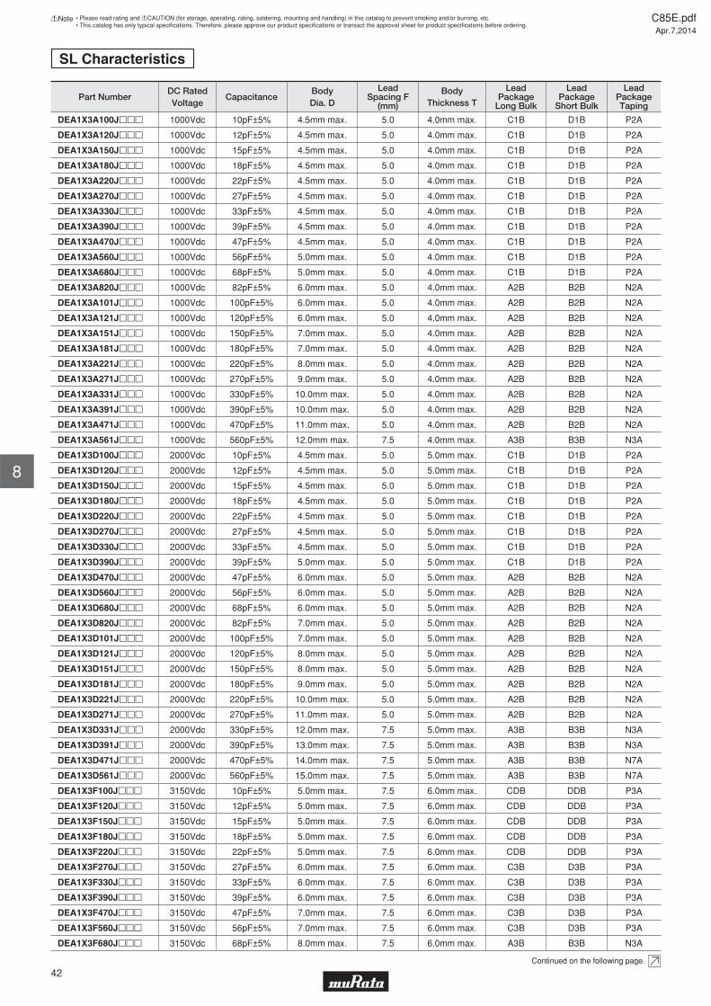
SL Characteristics
Part NumberDC RatedVoltage
CapacitanceBodyDia. D
LeadSpacing F
(mm)
BodyThickness T
LeadPackage
Long Bulk
LeadPackage
Short Bulk
LeadPackageTaping
DEA1X3A100Jppp 1000Vdc 10pF±5% 4.5mm max. 5.0 4.0mm max. C1B D1B P2A
DEA1X3A120Jppp 1000Vdc 12pF±5% 4.5mm max. 5.0 4.0mm max. C1B D1B P2A
DEA1X3A150Jppp 1000Vdc 15pF±5% 4.5mm max. 5.0 4.0mm max. C1B D1B P2A
DEA1X3A180Jppp 1000Vdc 18pF±5% 4.5mm max. 5.0 4.0mm max. C1B D1B P2A
DEA1X3A220Jppp 1000Vdc 22pF±5% 4.5mm max. 5.0 4.0mm max. C1B D1B P2A
DEA1X3A270Jppp 1000Vdc 27pF±5% 4.5mm max. 5.0 4.0mm max. C1B D1B P2A
DEA1X3A330Jppp 1000Vdc 33pF±5% 4.5mm max. 5.0 4.0mm max. C1B D1B P2A
DEA1X3A390Jppp 1000Vdc 39pF±5% 4.5mm max. 5.0 4.0mm max. C1B D1B P2A
DEA1X3A470Jppp 1000Vdc 47pF±5% 4.5mm max. 5.0 4.0mm max. C1B D1B P2A
DEA1X3A560Jppp 1000Vdc 56pF±5% 5.0mm max. 5.0 4.0mm max. C1B D1B P2A
DEA1X3A680Jppp 1000Vdc 68pF±5% 5.0mm max. 5.0 4.0mm max. C1B D1B P2A
DEA1X3A820Jppp 1000Vdc 82pF±5% 6.0mm max. 5.0 4.0mm max. A2B B2B N2A
DEA1X3A101Jppp 1000Vdc 100pF±5% 6.0mm max. 5.0 4.0mm max. A2B B2B N2A
DEA1X3A121Jppp 1000Vdc 120pF±5% 6.0mm max. 5.0 4.0mm max. A2B B2B N2A
DEA1X3A151Jppp 1000Vdc 150pF±5% 7.0mm max. 5.0 4.0mm max. A2B B2B N2A
DEA1X3A181Jppp 1000Vdc 180pF±5% 7.0mm max. 5.0 4.0mm max. A2B B2B N2A
DEA1X3A221Jppp 1000Vdc 220pF±5% 8.0mm max. 5.0 4.0mm max. A2B B2B N2A
DEA1X3A271Jppp 1000Vdc 270pF±5% 9.0mm max. 5.0 4.0mm max. A2B B2B N2A
DEA1X3A331Jppp 1000Vdc 330pF±5% 10.0mm max. 5.0 4.0mm max. A2B B2B N2A
DEA1X3A391Jppp 1000Vdc 390pF±5% 10.0mm max. 5.0 4.0mm max. A2B B2B N2A
DEA1X3A471Jppp 1000Vdc 470pF±5% 11.0mm max. 5.0 4.0mm max. A2B B2B N2A
DEA1X3A561Jppp 1000Vdc 560pF±5% 12.0mm max. 7.5 4.0mm max. A3B B3B N3A
DEA1X3D100Jppp 2000Vdc 10pF±5% 4.5mm max. 5.0 5.0mm max. C1B D1B P2A
DEA1X3D120Jppp 2000Vdc 12pF±5% 4.5mm max. 5.0 5.0mm max. C1B D1B P2A
DEA1X3D150Jppp 2000Vdc 15pF±5% 4.5mm max. 5.0 5.0mm max. C1B D1B P2A
DEA1X3D180Jppp 2000Vdc 18pF±5% 4.5mm max. 5.0 5.0mm max. C1B D1B P2A
DEA1X3D220Jppp 2000Vdc 22pF±5% 4.5mm max. 5.0 5.0mm max. C1B D1B P2A
DEA1X3D270Jppp 2000Vdc 27pF±5% 4.5mm max. 5.0 5.0mm max. C1B D1B P2A
DEA1X3D330Jppp 2000Vdc 33pF±5% 4.5mm max. 5.0 5.0mm max. C1B D1B P2A
DEA1X3D390Jppp 2000Vdc 39pF±5% 5.0mm max. 5.0 5.0mm max. C1B D1B P2A
DEA1X3D470Jppp 2000Vdc 47pF±5% 6.0mm max. 5.0 5.0mm max. A2B B2B N2A
DEA1X3D560Jppp 2000Vdc 56pF±5% 6.0mm max. 5.0 5.0mm max. A2B B2B N2A
DEA1X3D680Jppp 2000Vdc 68pF±5% 6.0mm max. 5.0 5.0mm max. A2B B2B N2A
DEA1X3D820Jppp 2000Vdc 82pF±5% 7.0mm max. 5.0 5.0mm max. A2B B2B N2A
DEA1X3D101Jppp 2000Vdc 100pF±5% 7.0mm max. 5.0 5.0mm max. A2B B2B N2A
DEA1X3D121Jppp 2000Vdc 120pF±5% 8.0mm max. 5.0 5.0mm max. A2B B2B N2A
DEA1X3D151Jppp 2000Vdc 150pF±5% 8.0mm max. 5.0 5.0mm max. A2B B2B N2A
DEA1X3D181Jppp 2000Vdc 180pF±5% 9.0mm max. 5.0 5.0mm max. A2B B2B N2A
DEA1X3D221Jppp 2000Vdc 220pF±5% 10.0mm max. 5.0 5.0mm max. A2B B2B N2A
DEA1X3D271Jppp 2000Vdc 270pF±5% 11.0mm max. 5.0 5.0mm max. A2B B2B N2A
DEA1X3D331Jppp 2000Vdc 330pF±5% 12.0mm max. 7.5 5.0mm max. A3B B3B N3A
DEA1X3D391Jppp 2000Vdc 390pF±5% 13.0mm max. 7.5 5.0mm max. A3B B3B N3A
DEA1X3D471Jppp 2000Vdc 470pF±5% 14.0mm max. 7.5 5.0mm max. A3B B3B N7A
DEA1X3D561Jppp 2000Vdc 560pF±5% 15.0mm max. 7.5 5.0mm max. A3B B3B N7A
DEA1X3F100Jppp 3150Vdc 10pF±5% 5.0mm max. 7.5 6.0mm max. CDB DDB P3A
DEA1X3F120Jppp 3150Vdc 12pF±5% 5.0mm max. 7.5 6.0mm max. CDB DDB P3A
DEA1X3F150Jppp 3150Vdc 15pF±5% 5.0mm max. 7.5 6.0mm max. CDB DDB P3A
DEA1X3F180Jppp 3150Vdc 18pF±5% 5.0mm max. 7.5 6.0mm max. CDB DDB P3A
DEA1X3F220Jppp 3150Vdc 22pF±5% 5.0mm max. 7.5 6.0mm max. CDB DDB P3A
DEA1X3F270Jppp 3150Vdc 27pF±5% 6.0mm max. 7.5 6.0mm max. C3B D3B P3A
DEA1X3F330Jppp 3150Vdc 33pF±5% 6.0mm max. 7.5 6.0mm max. C3B D3B P3A
DEA1X3F390Jppp 3150Vdc 39pF±5% 6.0mm max. 7.5 6.0mm max. C3B D3B P3A
DEA1X3F470Jppp 3150Vdc 47pF±5% 7.0mm max. 7.5 6.0mm max. C3B D3B P3A
DEA1X3F560Jppp 3150Vdc 56pF±5% 7.0mm max. 7.5 6.0mm max. C3B D3B P3A
DEA1X3F680Jppp 3150Vdc 68pF±5% 8.0mm max. 7.5 6.0mm max. A3B B3B N3A
Continued on the following page.
C85E.pdfApr.7,2014
42
!Note • Please read rating and !CAUTION (for storage, operating, rating, soldering, mounting and handling) in this catalog to prevent smoking and/or burning, etc.• This catalog has only typical specifi cations. Therefore, please approve our product specifi cations or transact the approval sheet for product specifi cations before ordering.
8

Continued from the preceding page.
Part NumberDC RatedVoltage
CapacitanceBodyDia. D
LeadSpacing F
(mm)
BodyThickness T
LeadPackage
Long Bulk
LeadPackage
Short Bulk
LeadPackageTaping
DEA1X3F820Jppp 3150Vdc 82pF±5% 8.0mm max. 7.5 6.0mm max. A3B B3B N3A
DEA1X3F101Jppp 3150Vdc 100pF±5% 9.0mm max. 7.5 6.0mm max. A3B B3B N3A
DEA1X3F121Jppp 3150Vdc 120pF±5% 10.0mm max. 7.5 6.0mm max. A3B B3B N3A
DEA1X3F151Jppp 3150Vdc 150pF±5% 11.0mm max. 7.5 6.0mm max. A3B B3B N3A
DEA1X3F181Jppp 3150Vdc 180pF±5% 11.0mm max. 7.5 6.0mm max. A3B B3B N3A
DEA1X3F221Jppp 3150Vdc 220pF±5% 12.0mm max. 7.5 6.0mm max. A3B B3B N3A
DEA1X3F271Jppp 3150Vdc 270pF±5% 14.0mm max. 7.5 6.0mm max. A3B B3B N7A
DEA1X3F331Jppp 3150Vdc 330pF±5% 15.0mm max. 7.5 6.0mm max. A3B B3B N7A
DEA1X3F391Jppp 3150Vdc 390pF±5% 16.0mm max. 7.5 6.0mm max. A3B B3B N7A
Three blank columns are fi lled with the lead and packaging codes. Please refer to the three columns on the right for the appropriate code.
C85E.pdfApr.7,2014
43
!Note • Please read rating and !CAUTION (for storage, operating, rating, soldering, mounting and handling) in this catalog to prevent smoking and/or burning, etc.• This catalog has only typical specifi cations. Therefore, please approve our product specifi cations or transact the approval sheet for product specifi cations before ordering.
8

DEA Series Specifi cations and Test Methods
Continued on the following page.
StepTemp. (°C) 20±2
1-25±3
220±2
385±2
420±2
5
*1 "Room condition" Temperature: 15 to 35°C, Relative humidity: 45 to 75%, Atmospheric pressure: 86 to 106kPa *2 "C" expresses nominal capacitance value (pF).
The lead wire should be immersed into the melted solder of 350±10°C (Body of ø5mm and under: 270±5°C) up to about 1.5 to 2mm from the main body for 3.5±0.5 sec. (Body of ø5mm and under: 5±0.5 sec.)Post-treatment:
Capacitor should be stored for 1 to 2 hrs. at room condition.*1
12Soldering Effect(Non-Preheat)
Appearance No marked defect
Capacitance Change
Within ±2.5%
Dielectric Strength (Between Lead Wires)
Per item 4.
The lead wire of a capacitor should be dipped into a ethanol solution of 25wt% rosin and then into molten solder for 2±0.5 sec. In both cases the depth of dipping is up to about 1.5 to 2mm from the root of lead wires.Temp. of solder: Lead Free Solder (Sn-3Ag-0.5Cu) 245±5°C H63 Eutectic Solder 235±5°C
11 Solderability of LeadsLead wire should be soldered with uniform coating on the axial direction over 3/4 of the circumferential direction.
The capacitor should be firmly soldered to the supporting lead wire and vibrated at a frequency range of 10 to 55Hz, 1.5mm in total amplitude, with about a 1-minute rate of vibration change from 10Hz to 55Hz and back to 10Hz. Apply for a total of 6 hrs., 2 hrs. each in 3 mutually perpendicular directions.
10Vibration Resistance
Appearance No marked defect
Capacitance Within specified tolerance
Q400+20C*2min. (30pF under) 1000 min. (30pF min.)
As shown in the figure at right, fix the body of the capacitor and apply a tensile weight gradually to each lead wire in the radial direction of the capacitor up to 10N (5N for lead diameter 0.5mm), and keep it for 10±1 sec.9 Strength of Lead
Pull
Lead wire should not be cut off.Capacitor should not be broken.
Bending
Each lead wire should be subjected to 5N (2.5N for lead diameter 0.5mm) of weight and bent 90° at the point of egress, in one direction, then returned to its original position and bent 90° in the opposite direction at the rate of one bend in 2 to 3 sec.
The capacitance measurement should be made at each step specified in the Table.
8 Temperature Characteristics
+350 to -1000ppm/°C(Temp. range: +20 to +85°C)
The Q should be measured at 20°C with 1±0.2MHz and AC5V(r.m.s.) max.
7 Q 400+20C*2min. (30pF under)1000 min. (30pF min.)
The capacitance should be measured at 20°C with 1±0.2MHz and AC5V(r.m.s.) max.
6 Capacitance Within specified tolerance
The insulation resistance should be measured with DC500±50V within 60±5 sec. of charging.
5Insulation Resistance (I.R.)
Between Lead Wires
10000MΩ min.
The capacitor should not be damaged when DC voltage of 200% of the rated voltage is applied between the lead wires for 1 to 5 sec. (Charge/Discharge currentV50mA)
4Dielectric Strength
Between Lead Wires
No failure
Body Insulation No failure
The capacitor is placed in the container with metal balls of diameter 1mm so that each lead wire, short circuited, is kept about 2mm off the metal balls as shown in the figure at right, and AC1250V(r.m.s.) <50/60Hz> is applied for 1 to 5 sec. between capacitor lead wires and metal balls.(Charge/Discharge currentV50mA)
The capacitor should be visually inspected.3 Marking To be easily legible
The capacitor should be visually inspected for evidence of defect. Dimensions should be measured with slide calipers.
2 Appearance and DimensionsNo visible defect, and dimensions are within specified range.
1 Operating Temperature Range -25 to +125°C
No. Test MethodSpecificationsItem
W
About 2mm
Metal balls
C85E.pdfApr.7,2014
44
!Note • Please read rating and !CAUTION (for storage, operating, rating, soldering, mounting and handling) in this catalog to prevent smoking and/or burning, etc.• This catalog has only typical specifi cations. Therefore, please approve our product specifi cations or transact the approval sheet for product specifi cations before ordering.
8

DEA Series Specifi cations and Test Methods
Continued from the preceding page.
Apply a DC voltage of 150% of the rated voltage for 1000+48/-0 hrs. at 125±2°C with a relative humidity of 50% max. (Charge/Discharge currentV50mA)Post-treatment:
Capacitor should be stored for 1 to 2 hrs. at room condition.*1
17 Life
Appearance No marked defect
Q275+5/2C*2min. (30pF under)350 min. (30pF min.)
Capacitance Change
Within ±3%
I.R. 2000MΩ min.
Apply the rated voltage for 500+24/-0 hrs. at 40±2°C in 90 to 95% relative humidity. (Charge/Discharge currentV50mA)Post-treatment:
Capacitor should be stored for 1 to 2 hrs. at room condition.*1
16Humidity Loading
Appearance No marked defect
Q275+5/2C*2min. (30pF under)350 min. (30pF min.)
Capacitance Change
Within ±5%
I.R. 1000MΩ min.
Set the capacitor for 500+24/-0 hrs. at 40±2°C in 90 to 95% relative humidity.
Post-treatment:Capacitor should be stored for 1 to 2 hrs. at room condition.*1
15Humidity (Under Steady State)
Appearance No marked defect
Q275+5/2C*2min. (30pF under)350 min. (30pF min.)
Capacitance Change
Within ±5%
I.R. 1000MΩ min.
The capacitor should be subjected to 5 temperature cycles.<Temperature Cycle>
Post-treatment:Capacitor should be stored for 1 to 2 hrs. at room condition.*1
14Temperature Cycle
Appearance No marked defect
I.R. 1000MΩ min.
Q275+5/2C*2min. (30pF under)350 min. (30pF min.)
Capacitance Change
Within ±5%
Dielectric Strength (Between Lead Wires)
Per item 4.
First the capacitor should be stored at 120+0/-5°C for 60+0/-5 sec. Then, as in the figure, the lead wires should be immersed in solder of 260+0/-5°C up to 1.5 to 2.0mm from the root of terminal for 7.5+0/-1 sec.Post-treatment:
Capacitor should be stored for 1 to 2 hrs. at room condition.*1
13Soldering Effect(On-Preheat)
Appearance No marked defect
Capacitance Change
Within ±2.5%
Dielectric Strength (Between Lead Wires)
Per item 4.
Step Temperature (°C)-25±3
Room Temp.125±3
Room Temp.
Time (min)303
303
Cycle time: 5 cycles
1234
No. Test MethodSpecificationsItem
*1 "Room condition" Temperature: 15 to 35°C, Relative humidity: 45 to 75%, Atmospheric pressure: 86 to 106kPa *2 "C" expresses nominal capacitance value (pF).
ThermalScreen
Capacitor
1.5to 2.0mm
MoltenSolder
C85E.pdfApr.7,2014
45
!Note • Please read rating and !CAUTION (for storage, operating, rating, soldering, mounting and handling) in this catalog to prevent smoking and/or burning, etc.• This catalog has only typical specifi cations. Therefore, please approve our product specifi cations or transact the approval sheet for product specifi cations before ordering.
8

High Voltage Ceramic CapacitorsDEB Series (Class 2/DC1k-3.15kV)
c Features1. Small size and high capacitance2. Coated with fl ame-retardant epoxy resin (equivalent to UL94V-0 standard). Please contact us when a halogen-free product* is necessary. * Cl=900ppm max., Br=900ppm max. and Cl+Br=1500ppm max.3. Taping available for automatic insertion.
c ApplicationsIdeal for use on decoupling circuits for power supplies. Do not use these products in any automotive power train or safety equipment including battery chargers for electric vehicles and plug-in hybrids.Only Murata products clearly stipulated as "for Automotive use" on its catalog can be used for automobile applications such as power train and safety equipment.
Lead Code Coating Extension e
A2, A3
C1, CD
C3
Up to the end of crimp
3.0 max.
3.0 max.
(in mm)
ø d
0.6±0.05
0.5±0.05
0.6±0.05
Style
Fig. 1
Fig. 2
Fig. 2
D max. T max.T max.
<Fig. 1> <Fig. 2>
3.0
max
.
25.0
min
.
e
ø d
25.0
min
.
F±1.0
D max. T max.T max.
<Fig. 1> <Fig. 2>
3.0
max
.
5.0±
1.0
F±0.8
e
ø d 5.0±
1.0
Lead Code Coating Extension e
B2, B3
D1, DD
D3
Up to the end of crimp
3.0 max.
3.0 max.
(in mm)
ø d
0.6±0.05
0.5±0.05
0.6±0.05
Style
Fig. 1
Fig. 2
Fig. 2
EB F
ø4.5-5mm
ø6mm
ø7-9mm
ø10-16mm
Temperature Characteristics
Nominal Capacitance
Capacitance Tolerance
Rated Voltage
Manufacturer's Identification
Manufactured Date Code
Marked with code for char. B and E (omitted for nominal body diameter ø9mm and under)
Marked with 3 figures
Marked with code (omitted for nominal body diameter ø6mm and under)
Marked with code (for DC3.15kV, marked with 3KV)
Marked with (omitted for nominal body diameter ø9mm and under)
Abbreviation (omitted for nominal body diameter ø5mm and under)
Temp. Char.
Nominal Body Diameter
1022KV66
1021KV
102Z3KV66
B332K3KV
66
E472Z3KV
66
103Z2KV
66
3313KV66
2213KV
102K3KV66
2221KV66
1022KV
472Z2KV66
c Marking
C85E.pdfApr.7,2014
46
!Note • Please read rating and !CAUTION (for storage, operating, rating, soldering, mounting and handling) in this catalog to prevent smoking and/or burning, etc.• This catalog has only typical specifi cations. Therefore, please approve our product specifi cations or transact the approval sheet for product specifi cations before ordering.
9
[Bulk]Vertical Crimp Long (Fig. 1)
Straight Long (Fig. 2)
[Bulk]Vertical Crimp Short (Fig. 1)
Straight Short (Fig. 2)

B Characteristics
Part NumberDC RatedVoltage
CapacitanceBodyDia. D
LeadSpacing F
(mm)
BodyThickness T
LeadPackage
Long Bulk
LeadPackage
Short Bulk
LeadPackageTaping
DEBB33A101Kppp 1000Vdc 100pF±10% 4.5mm max. 5.0 4.0mm max. C1B D1B P2A
DEBB33A151Kppp 1000Vdc 150pF±10% 4.5mm max. 5.0 4.0mm max. C1B D1B P2A
DEBB33A221Kppp 1000Vdc 220pF±10% 4.5mm max. 5.0 4.0mm max. C1B D1B P2A
DEBB33A331Kppp 1000Vdc 330pF±10% 4.5mm max. 5.0 4.0mm max. C1B D1B P2A
DEBB33A471Kppp 1000Vdc 470pF±10% 5.0mm max. 5.0 4.0mm max. C1B D1B P2A
DEBB33A681Kppp 1000Vdc 680pF±10% 6.0mm max. 5.0 4.0mm max. A2B B2B N2A
DEBB33A102Kppp 1000Vdc 1000pF±10% 6.0mm max. 5.0 4.0mm max. A2B B2B N2A
DEBB33A152Kppp 1000Vdc 1500pF±10% 8.0mm max. 5.0 4.0mm max. A2B B2B N2A
DEBB33A222Kppp 1000Vdc 2200pF±10% 9.0mm max. 5.0 4.0mm max. A2B B2B N2A
DEBB33A332Kppp 1000Vdc 3300pF±10% 10.0mm max. 5.0 4.0mm max. A2B B2B N2A
DEBB33A472Kppp 1000Vdc 4700pF±10% 12.0mm max. 7.5 4.0mm max. A3B B3B N3A
DEBB33A682Kppp 1000Vdc 6800pF±10% 15.0mm max. 7.5 4.0mm max. A3B B3B N7A
DEBB33D101Kppp 2000Vdc 100pF±10% 4.5mm max. 5.0 5.0mm max. C1B D1B P2A
DEBB33D151Kppp 2000Vdc 150pF±10% 4.5mm max. 5.0 5.0mm max. C1B D1B P2A
DEBB33D221Kppp 2000Vdc 220pF±10% 4.5mm max. 5.0 5.0mm max. C1B D1B P2A
DEBB33D331Kppp 2000Vdc 330pF±10% 5.0mm max. 5.0 5.0mm max. C1B D1B P2A
DEBB33D471Kppp 2000Vdc 470pF±10% 6.0mm max. 5.0 5.0mm max. A2B B2B N2A
DEBB33D681Kppp 2000Vdc 680pF±10% 7.0mm max. 5.0 5.0mm max. A2B B2B N2A
DEBB33D102Kppp 2000Vdc 1000pF±10% 8.0mm max. 5.0 5.0mm max. A2B B2B N2A
DEBB33D152Kppp 2000Vdc 1500pF±10% 9.0mm max. 5.0 5.0mm max. A2B B2B N2A
DEBB33D222Kppp 2000Vdc 2200pF±10% 10.0mm max. 5.0 5.0mm max. A2B B2B N2A
DEBB33D332Kppp 2000Vdc 3300pF±10% 12.0mm max. 7.5 5.0mm max. A3B B3B N3A
DEBB33D472Kppp 2000Vdc 4700pF±10% 15.0mm max. 7.5 5.0mm max. A3B B3B N7A
DEBB33F101Kppp 3150Vdc 100pF±10% 5.0mm max. 7.5 6.0mm max. CDB DDB P3A
DEBB33F151Kppp 3150Vdc 150pF±10% 5.0mm max. 7.5 6.0mm max. CDB DDB P3A
DEBB33F221Kppp 3150Vdc 220pF±10% 5.0mm max. 7.5 6.0mm max. CDB DDB P3A
DEBB33F331Kppp 3150Vdc 330pF±10% 6.0mm max. 7.5 6.0mm max. C3B D3B P3A
DEBB33F471Kppp 3150Vdc 470pF±10% 7.0mm max. 7.5 6.0mm max. C3B D3B P3A
DEBB33F681Kppp 3150Vdc 680pF±10% 8.0mm max. 7.5 6.0mm max. A3B B3B N3A
DEBB33F102Kppp 3150Vdc 1000pF±10% 9.0mm max. 7.5 6.0mm max. A3B B3B N3A
DEBB33F152Kppp 3150Vdc 1500pF±10% 11.0mm max. 7.5 6.0mm max. A3B B3B N3A
DEBB33F222Kppp 3150Vdc 2200pF±10% 13.0mm max. 7.5 6.0mm max. A3B B3B N3A
DEBB33F332Kppp 3150Vdc 3300pF±10% 15.0mm max. 7.5 6.0mm max. A3B B3B N7A
Three blank columns are fi lled with the lead and packaging codes. Please refer to the three columns on the right for the appropriate code.
E Characteristics
Part NumberDC RatedVoltage
CapacitanceBodyDia. D
LeadSpacing F
(mm)
BodyThickness T
LeadPackage
Long Bulk
LeadPackage
Short Bulk
LeadPackageTaping
DEBE33A102Zppp 1000Vdc 1000pF+80/-20% 5.0mm max. 5.0 4.0mm max. C1B D1B P2A
DEBE33A222Zppp 1000Vdc 2200pF+80/-20% 7.0mm max. 5.0 4.0mm max. A2B B2B N2A
DEBE33A472Zppp 1000Vdc 4700pF+80/-20% 9.0mm max. 5.0 4.0mm max. A2B B2B N2A
DEBE33A103Zppp 1000Vdc 10000pF+80/-20% 13.0mm max. 7.5 4.0mm max. A3B B3B N3A
DEBE33D102Zppp 2000Vdc 1000pF+80/-20% 6.0mm max. 5.0 5.0mm max. A2B B2B N2A
DEBE33D222Zppp 2000Vdc 2200pF+80/-20% 8.0mm max. 5.0 5.0mm max. A2B B2B N2A
DEBE33D472Zppp 2000Vdc 4700pF+80/-20% 11.0mm max. 5.0 5.0mm max. A2B B2B N2A
DEBE33D103Zppp 2000Vdc 10000pF+80/-20% 16.0mm max. 7.5 5.0mm max. A3B B3B N7A
DEBE33F102Zppp 3150Vdc 1000pF+80/-20% 7.0mm max. 7.5 6.0mm max. C3B D3B P3A
DEBE33F222Zppp 3150Vdc 2200pF+80/-20% 10.0mm max. 7.5 6.0mm max. A3B B3B N3A
DEBE33F472Zppp 3150Vdc 4700pF+80/-20% 13.0mm max. 7.5 6.0mm max. A3B B3B N3A
Three blank columns are fi lled with the lead and packaging codes. Please refer to the three columns on the right for the appropriate code.
C85E.pdfApr.7,2014
47
!Note • Please read rating and !CAUTION (for storage, operating, rating, soldering, mounting and handling) in this catalog to prevent smoking and/or burning, etc.• This catalog has only typical specifi cations. Therefore, please approve our product specifi cations or transact the approval sheet for product specifi cations before ordering.
9

F Characteristics
Part NumberDC RatedVoltage
CapacitanceBodyDia. D
LeadSpacing F
(mm)
BodyThickness T
LeadPackage
Long Bulk
LeadPackage
Short Bulk
LeadPackageTaping
DEBF33A222Zppp 1000Vdc 2200pF+80/-20% 6.0mm max. 5.0 4.0mm max. A2B B2B N2A
DEBF33A472Zppp 1000Vdc 4700pF+80/-20% 7.0mm max. 5.0 4.0mm max. A2B B2B N2A
DEBF33A103Zppp 1000Vdc 10000pF+80/-20% 10.0mm max. 5.0 4.0mm max. A2B B2B N2A
DEBF33D102Zppp 2000Vdc 1000pF+80/-20% 5.0mm max. 5.0 5.0mm max. C1B D1B P2A
DEBF33D222Zppp 2000Vdc 2200pF+80/-20% 7.0mm max. 5.0 5.0mm max. A2B B2B N2A
DEBF33D472Zppp 2000Vdc 4700pF+80/-20% 9.0mm max. 5.0 5.0mm max. A2B B2B N2A
DEBF33D103Zppp 2000Vdc 10000pF+80/-20% 12.0mm max. 7.5 5.0mm max. A3B B3B N3A
Three blank columns are fi lled with the lead and packaging codes. Please refer to the three columns on the right for the appropriate code.
C85E.pdfApr.7,2014
48
!Note • Please read rating and !CAUTION (for storage, operating, rating, soldering, mounting and handling) in this catalog to prevent smoking and/or burning, etc.• This catalog has only typical specifi cations. Therefore, please approve our product specifi cations or transact the approval sheet for product specifi cations before ordering.
9

DEB Series Specifi cations and Test Methods
Continued on the following page.
StepTemp. (°C)
120±2
2-25±3
320±2
485±2
520±2
* "Room condition" Temperature: 15 to 35°C, Relative humidity: 45 to 75%, Atmospheric pressure: 86 to 106kPa
About 2mm
Metal balls
W
The lead wire should be immersed into the melted solder of 350±10°C (Body of ø5mm and under: 270±5°C) up to about 1.5 to 2mm from the main body for 3.5±0.5 sec. (Body of ø5mm and under: 5±0.5 sec.)Pre-treatment: Capacitor should be stored at 85±2°C for 1 hr.,
then placed at room condition* for 24±2 hrs. before initial measurements.
Post-treatment: Capacitor should be stored for 4 to 24 hrs. at room condition.*
12Soldering Effect(Non-Preheat)
Appearance No marked defect
Capacitance Change
Char. B: Within ±5%Char. E: Within ±15%Char. F: Within ±20%
Dielectric Strength (Between Lead Wires)
Per item 4.
The lead wire of a capacitor should be dipped into a ethanol solution of 25wt% rosin and then into molten solder for 2±0.5 sec. In both cases the depth of dipping is up to about 1.5 to 2mm from the root of lead wires. Temp. of solder: Lead Free Solder (Sn-3Ag-0.5Cu) 245±5°C H63 Eutectic Solder 235±5°C
11 Solderability of LeadsLead wire should be soldered with uniform coating on the axial direction over 3/4 of the circumferential direction.
The capacitor should be firmly soldered to the supporting lead wire and vibrated at a frequency range of 10 to 55Hz, 1.5mm in total amplitude, with about a 1-minute rate of vibration change from 10Hz to 55Hz and back to 10Hz. Apply for a total of 6 hrs., 2 hrs. each in 3 mutually perpendicular directions.
10Vibration Resistance
Appearance No marked defect
Capacitance Within specified tolerance
D.F.Char. B, E: 2.5% max.Char. F: 5.0% max.
As shown in the figure at right, fix the body of the capacitor and apply a tensile weight gradually to each lead wire in the radial direction of the capacitor up to 10N (5N for lead diameter 0.5mm), and keep it for 10±1 sec.9 Strength of Lead
Pull
Lead wire should not be cut off.Capacitor should not be broken.
Bending
Each lead wire should be subjected to 5N (2.5N for lead diameter 0.5mm) of weight and bent 90° at the point of egress, in one direction, then returned to its original position and bent 90° in the opposite direction at the rate of one bend in 2 to 3 sec.
The capacitance measurement should be made at each step specified in the Table.
Pre-treatment: Capacitor should be stored at 85±2°C for 1 hr., then placed at room condition* for 24±2 hrs. before measurements.
8 Temperature Characteristics
Char. B: Within ±10%Char. E: Within +20/-55%Char. F: Within +30/-80%
The dissipation factor should be measured at 20°C with 1±0.2kHz and AC5V(r.m.s.) max.
7 Dissipation Factor (D.F.)Char. B, E: 2.5% max.Char. F: 5.0% max.
The capacitance should be measured at 20°C with 1±0.2kHz and AC5V(r.m.s.) max.
6 Capacitance Within specified tolerance
The insulation resistance should be measured with DC500±50V within 60±5 sec. of charging.
5Insulation Resistance (I.R.)
Between Lead Wires
10000MΩ min.
The capacitor should not be damaged when DC voltage of 200% of the rated voltage is applied between the lead wires for 1 to 5 sec. (Charge/Discharge currentV50mA)
4Dielectric Strength
Between Lead Wires
No failure
Body Insulation No failure
The capacitor is placed in the container with metal balls of diameter 1mm so that each lead wire, short circuited, is kept about 2mm off the metal balls as shown in the figure at right, and DC voltage of 1.3kV is applied for 1 to 5 sec. between capacitor lead wires and metal balls.(Charge/Discharge currentV50mA)
The capacitor should be visually inspected.3 Marking To be easily legible
The capacitor should be visually inspected for evidence of defect. Dimensions should be measured with slide calipers.
2 Appearance and DimensionsNo visible defect, and dimensions are within specified range.
1 Operating Temperature Range -25 to +85°C
No. Test MethodSpecificationsItem
C85E.pdfApr.7,2014
49
!Note • Please read rating and !CAUTION (for storage, operating, rating, soldering, mounting and handling) in this catalog to prevent smoking and/or burning, etc.• This catalog has only typical specifi cations. Therefore, please approve our product specifi cations or transact the approval sheet for product specifi cations before ordering.
9
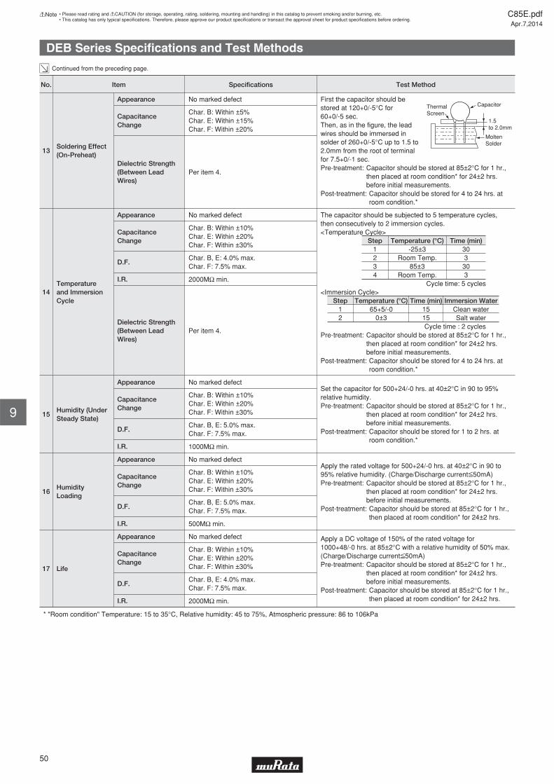
DEB Series Specifi cations and Test Methods
Continued from the preceding page.
Step Temperature (°C)-25±3
Room Temp.85±3
Room Temp.
Time (min)303
303
1234
Step Temperature (°C)65+5/-0
0±3
Time (min)1515
Immersion WaterClean waterSalt water
12
* "Room condition" Temperature: 15 to 35°C, Relative humidity: 45 to 75%, Atmospheric pressure: 86 to 106kPa
ThermalScreen
Capacitor
1.5to 2.0mm
MoltenSolder
Apply a DC voltage of 150% of the rated voltage for 1000+48/-0 hrs. at 85±2°C with a relative humidity of 50% max. (Charge/Discharge currentV50mA)Pre-treatment: Capacitor should be stored at 85±2°C for 1 hr.,
then placed at room condition* for 24±2 hrs. before initial measurements.
Post-treatment: Capacitor should be stored at 85±2°C for 1 hr., then placed at room condition* for 24±2 hrs.
17 Life
Appearance No marked defect
D.F.Char. B, E: 4.0% max.Char. F: 7.5% max.
Capacitance Change
Char. B: Within ±10%Char. E: Within ±20%Char. F: Within ±30%
I.R. 2000MΩ min.
Apply the rated voltage for 500+24/-0 hrs. at 40±2°C in 90 to 95% relative humidity. (Charge/Discharge currentV50mA)Pre-treatment: Capacitor should be stored at 85±2°C for 1 hr.,
then placed at room condition* for 24±2 hrs. before initial measurements.
Post-treatment: Capacitor should be stored at 85±2°C for 1 hr., then placed at room condition* for 24±2 hrs.
16Humidity Loading
Appearance No marked defect
D.F.Char. B, E: 5.0% max.Char. F: 7.5% max.
Capacitance Change
Char. B: Within ±10%Char. E: Within ±20%Char. F: Within ±30%
I.R. 500MΩ min.
Set the capacitor for 500+24/-0 hrs. at 40±2°C in 90 to 95% relative humidity.Pre-treatment: Capacitor should be stored at 85±2°C for 1 hr.,
then placed at room condition* for 24±2 hrs. before initial measurements.
Post-treatment: Capacitor should be stored for 1 to 2 hrs. at room condition.*
15Humidity (Under Steady State)
Appearance No marked defect
D.F.Char. B, E: 5.0% max.Char. F: 7.5% max.
Capacitance Change
Char. B: Within ±10%Char. E: Within ±20%Char. F: Within ±30%
I.R. 1000MΩ min.
The capacitor should be subjected to 5 temperature cycles, then consecutively to 2 immersion cycles. <Temperature Cycle>
Cycle time: 5 cycles<Immersion Cycle>
Cycle time : 2 cyclesPre-treatment: Capacitor should be stored at 85±2°C for 1 hr.,
then placed at room condition* for 24±2 hrs. before initial measurements.
Post-treatment: Capacitor should be stored for 4 to 24 hrs. at room condition.*
14Temperature and Immersion Cycle
Appearance No marked defect
I.R. 2000MΩ min.
D.F.Char. B, E: 4.0% max.Char. F: 7.5% max.
Capacitance Change
Char. B: Within ±10%Char. E: Within ±20%Char. F: Within ±30%
Dielectric Strength (Between Lead Wires)
Per item 4.
First the capacitor should be stored at 120+0/-5°C for 60+0/-5 sec. Then, as in the figure, the lead wires should be immersed in solder of 260+0/-5°C up to 1.5 to 2.0mm from the root of terminal for 7.5+0/-1 sec.Pre-treatment: Capacitor should be stored at 85±2°C for 1 hr.,
then placed at room condition* for 24±2 hrs. before initial measurements.
Post-treatment: Capacitor should be stored for 4 to 24 hrs. at room condition.*
13Soldering Effect(On-Preheat)
Appearance No marked defect
Capacitance Change
Char. B: Within ±5%Char. E: Within ±15%Char. F: Within ±20%
Dielectric Strength (Between Lead Wires)
Per item 4.
No. Test MethodSpecificationsItem
C85E.pdfApr.7,2014
50
!Note • Please read rating and !CAUTION (for storage, operating, rating, soldering, mounting and handling) in this catalog to prevent smoking and/or burning, etc.• This catalog has only typical specifi cations. Therefore, please approve our product specifi cations or transact the approval sheet for product specifi cations before ordering.
9
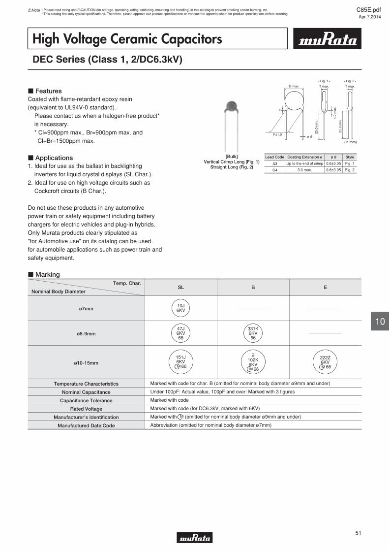
High Voltage Ceramic CapacitorsDEC Series (Class 1, 2/DC6.3kV)
c FeaturesCoated with fl ame-retardant epoxy resin(equivalent to UL94V-0 standard). Please contact us when a halogen-free product* is necessary. * Cl=900ppm max., Br=900ppm max. and Cl+Br=1500ppm max.
c Applications1. Ideal for use as the ballast in backlighting inverters for liquid crystal displays (SL Char.).2. Ideal for use on high voltage circuits such as Cockcroft circuits (B Char.). Do not use these products in any automotive power train or safety equipment including battery chargers for electric vehicles and plug-in hybrids.Only Murata products clearly stipulated as "for Automotive use" on its catalog can be used for automobile applications such as power train and safety equipment.
D max. T max.
e
ø d
25.0
min
.
F±1.0
T max.
<Fig. 1>
4.0
max
.
25.0
min
.
<Fig. 2>
Lead Code Coating Extension e
A3
C4
Up to the end of crimp
3.0 max.
ø d
0.6±0.05
0.6±0.05
Style
Fig. 1
Fig. 2
(in mm)
[Bulk]Vertical Crimp Long (Fig. 1)
Straight Long (Fig. 2)
BSL E
ø7mm
ø8-9mm
ø10-15mm
Temperature Characteristics
Nominal Capacitance
Capacitance Tolerance
Rated Voltage
Manufacturer's Identification
Manufactured Date Code
Marked with code for char. B (omitted for nominal body diameter ø9mm and under)
Under 100pF: Actual value, 100pF and over: Marked with 3 figures
Marked with code
Marked with code (for DC6.3kV, marked with 6KV)
Marked with (omitted for nominal body diameter ø9mm and under)
Abbreviation (omitted for nominal body diameter ø7mm)
Temp. Char.
Nominal Body Diameter
151J6KV
66
B102K6KV
66
222Z6KV
66
47J6KV66
331K6KV66
10J6KV
c Marking
C85E.pdfApr.7,2014
51
!Note • Please read rating and !CAUTION (for storage, operating, rating, soldering, mounting and handling) in this catalog to prevent smoking and/or burning, etc.• This catalog has only typical specifi cations. Therefore, please approve our product specifi cations or transact the approval sheet for product specifi cations before ordering.
10

SL Characteristics
Part NumberDC RatedVoltage
CapacitanceBodyDia. D
LeadSpacing F
(mm)
BodyThickness T
DEC1X3J100JA3BMS1 6300Vdc 10pF±5% 7.0mm max. 7.5 7.0mm max.
DEC1X3J100JC4BMS1 6300Vdc 10pF±5% 7.0mm max. 10.0 7.0mm max.
DEC1X3J120JA3B 6300Vdc 12pF±5% 8.0mm max. 7.5 7.0mm max.
DEC1X3J120JC4B 6300Vdc 12pF±5% 8.0mm max. 10.0 7.0mm max.
DEC1X3J150JA3B 6300Vdc 15pF±5% 8.0mm max. 7.5 7.0mm max.
DEC1X3J150JC4B 6300Vdc 15pF±5% 8.0mm max. 10.0 7.0mm max.
DEC1X3J180JA3B 6300Vdc 18pF±5% 9.0mm max. 7.5 7.0mm max.
DEC1X3J180JC4B 6300Vdc 18pF±5% 9.0mm max. 10.0 7.0mm max.
DEC1X3J220JA3B 6300Vdc 22pF±5% 9.0mm max. 7.5 7.0mm max.
DEC1X3J220JC4B 6300Vdc 22pF±5% 9.0mm max. 10.0 7.0mm max.
DEC1X3J270JA3B 6300Vdc 27pF±5% 9.0mm max. 7.5 7.0mm max.
DEC1X3J270JC4B 6300Vdc 27pF±5% 9.0mm max. 10.0 7.0mm max.
DEC1X3J330JA3B 6300Vdc 33pF±5% 9.0mm max. 7.5 7.0mm max.
DEC1X3J330JC4B 6300Vdc 33pF±5% 9.0mm max. 10.0 7.0mm max.
DEC1X3J390JA3B 6300Vdc 39pF±5% 9.0mm max. 7.5 7.0mm max.
DEC1X3J390JC4B 6300Vdc 39pF±5% 9.0mm max. 10.0 7.0mm max.
DEC1X3J470JA3B 6300Vdc 47pF±5% 9.0mm max. 7.5 7.0mm max.
DEC1X3J470JC4B 6300Vdc 47pF±5% 9.0mm max. 10.0 7.0mm max.
DEC1X3J560JC4B 6300Vdc 56pF±5% 10.0mm max. 10.0 7.0mm max.
DEC1X3J680JC4B 6300Vdc 68pF±5% 12.0mm max. 10.0 7.0mm max.
DEC1X3J820JC4B 6300Vdc 82pF±5% 12.0mm max. 10.0 7.0mm max.
DEC1X3J101JC4B 6300Vdc 100pF±5% 13.0mm max. 10.0 7.0mm max.
DEC1X3J121JC4B 6300Vdc 120pF±5% 14.0mm max. 10.0 7.0mm max.
DEC1X3J151JC4B 6300Vdc 150pF±5% 15.0mm max. 10.0 7.0mm max.
B Characteristics
Part NumberDC RatedVoltage
CapacitanceBodyDia. D
LeadSpacing F
(mm)
BodyThickness T
DECB33J101KC4B 6300Vdc 100pF±10% 9.0mm max. 10.0 7.0mm max.
DECB33J151KC4B 6300Vdc 150pF±10% 9.0mm max. 10.0 7.0mm max.
DECB33J221KC4B 6300Vdc 220pF±10% 9.0mm max. 10.0 7.0mm max.
DECB33J331KC4B 6300Vdc 330pF±10% 9.0mm max. 10.0 7.0mm max.
DECB33J471KC4B 6300Vdc 470pF±10% 10.0mm max. 10.0 7.0mm max.
DECB33J681KC4B 6300Vdc 680pF±10% 11.0mm max. 10.0 7.0mm max.
DECB33J102KC4B 6300Vdc 1000pF±10% 13.0mm max. 10.0 7.0mm max.
E Characteristics
Part NumberDC RatedVoltage
CapacitanceBodyDia. D
LeadSpacing F
(mm)
BodyThickness T
DECE33J102ZC4B 6300Vdc 1000pF+80/-20% 11.0mm max. 10.0 7.0mm max.
DECE33J222ZC4B 6300Vdc 2200pF+80/-20% 15.0mm max. 10.0 7.0mm max.
C85E.pdfApr.7,2014
52
!Note • Please read rating and !CAUTION (for storage, operating, rating, soldering, mounting and handling) in this catalog to prevent smoking and/or burning, etc.• This catalog has only typical specifi cations. Therefore, please approve our product specifi cations or transact the approval sheet for product specifi cations before ordering.
10

DEC Series Specifi cations and Test Methods
StepTemp. (°C)
120±2
2-25±3
320±2
485±2
520±2
*1 "Room condition" Temperature: 15 to 35°C, Relative humidity: 45 to 75%, Atmospheric pressure: 86 to 106kPa *2 "C" expresses nominal capacitance value (pF).
The lead wire should be immersed into the melted solder of 350±10°C up to about 1.5 to 2mm from the main body for 3.5±0.5 sec. Pre-treatment: Capacitor should be stored at 85±2°C for 1 hr.,
then placed at room condition*1 for 24±2 hrs. before initial measurements. (Char. B, E)
Post-treatment: Capacitor should be stored for 1 to 2 hrs. at room condition.*1 (Char. SL)
Post-treatment: Capacitor should be stored for 4 to 24 hrs. at room condition.*1 (Char. B, E)
12Soldering Effect(Non-Preheat)
Appearance No marked defect
Capacitance Change
Char. SL: Within ±2.5%Char. B: Within ±5%Char. E: Within ±15%
Dielectric Strength (Between Lead Wires)
Per item 4.
The lead wire of a capacitor should be dipped into a ethanol solution of 25wt% rosin and then into molten solder for 2±0.5 sec. In both cases the depth of dipping is up to about 1.5 to 2mm from the root of lead wires. Temp. of solder: Lead Free Solder (Sn-3Ag-0.5Cu) 245±5°C H63 Eutectic Solder 235±5°C
11 Solderability of LeadsLead wire should be soldered with uniform coating on the axial direction over 3/4 of the circumferential direction.
The capacitor should be firmly soldered to the supporting lead wire and vibrated at a frequency range of 10 to 55Hz, 1.5mm in total amplitude, with about a 1-minute rate of vibration change from 10Hz to 55Hz and back to 10Hz. Apply for a total of 6 hrs., 2 hrs. each in 3 mutually perpendicular directions.
10Vibration Resistance
Appearance No marked defect
QChar. SL: 400+20C*2min. (30pF under) 1000 min. (30pF min.)
Capacitance Within specified tolerance
D.F. Char. B, E: 2.5% max.
As shown in the figure at right, fix the body of the capacitor and apply a tensile weight gradually to each lead wire in the radial direction of the capacitor up to 10N and keep it for 10±1 sec.9 Strength of Lead
Pull
Lead wire should not be cut off.Capacitor should not be broken.
Bending
Each lead wire should be subjected to 5N of weight and bent 90° at the point of egress, in one direction, then returned to its original position and bent 90° in the opposite direction at the rate of one bend in 2 to 3 sec.
The capacitance measurement should be made at each step specified in the Table.
Pre-treatment: Capacitor should be stored at 85±2°C for 1 hr., then placed at room condition*1 for 24±2 hrs. before measurements. (Char. B, E)
8 Temperature Characteristics
Char. SL: +350 to -1000ppm/°C(Temp. range: +20 to +85°C)
Char. B: Within ±10%Char. E: Within +20/-55%
The dissipation factor and Q should be measured at 20°C with 1±0.2kHz (Char. SL: 1±0.2MHz) and AC5V(r.m.s.) max.
7Q
Char. SL: 400+20C*2min. (30pF under) 1000 min. (30pF min.)
The capacitance should be measured at 20°C with 1±0.2kHz (Char. SL: 1±0.2MHz) and AC5V(r.m.s.) max.
6 Capacitance Within specified tolerance
The insulation resistance should be measured with DC500±50V within 60±5 sec. of charging.
5Insulation Resistance (I.R.)
Between Lead Wires
10000MΩ min.
The capacitor should not be damaged when DC voltage of 200% of the rated voltage is applied between the lead wires for 1 to 5 sec. (Charge/Discharge currentV50mA)
4Dielectric Strength
Between Lead Wires
No failure
Body Insulation No failure
The capacitor is placed in the container with metal balls of diameter 1mm so that each lead wire, short circuited, is kept about 2mm off the metal balls as shown in the figure at right, and DC voltage of 1.3kV is applied for 1 to 5 sec. between capacitor lead wires and metal balls.(Charge/Discharge currentV50mA)
The capacitor should be visually inspected.3 Marking To be easily legible
The capacitor should be visually inspected for evidence of defect. Dimensions should be measured with slide calipers.
2 Appearance and DimensionsNo visible defect, and dimensions are within specified range.
1 Operating Temperature Range -25 to +85°C
No. Test MethodSpecificationsItem
Dissipation Factor (D.F.) Char. B, E: 2.5% max.
W
About 2mm
Metal balls
Continued on the following page.
C85E.pdfApr.7,2014
53
!Note • Please read rating and !CAUTION (for storage, operating, rating, soldering, mounting and handling) in this catalog to prevent smoking and/or burning, etc.• This catalog has only typical specifi cations. Therefore, please approve our product specifi cations or transact the approval sheet for product specifi cations before ordering.
10

DEC Series Specifi cations and Test Methods
Continued from the preceding page.
Apply a DC voltage of 150% of the rated voltage for 1000+48/-0 hrs. at 85±2°C with a relative humidity of 50% max. (Charge/Discharge currentV50mA.)Pre-treatment: Capacitor should be stored at 85±2°C for 1 hr.,
then placed at room condition*1 for 24±2 hrs. before initial measurements. (Char. B, E)
Post-treatment: Capacitor should be stored for 1 to 2 hrs. at room condition.*1 (Char. SL)
Post-treatment: Capacitor should be stored at 85±2°C for 1 hr., then placed at room condition*1 for 24±2 hrs. (Char. B, E)
17 Life
Appearance No marked defect
D.F. Char. B, E: 4.0% max.
QChar. SL: 275+5/2C*2min. (30pF under) 350 min. (30pF min.)
Capacitance Change
Char. SL: Within ±3%Char. B: Within ±10%Char. E: Within ±20%
I.R. 2000MΩ min.
Apply the rated voltage for 500+24/-0 hrs. at 40±2°C in 90 to 95% relative humidity. (Charge/Discharge currentV50mA.)Pre-treatment: Capacitor should be stored at 85±2°C for 1 hr.,
then placed at room condition*1 for 24±2 hrs. before initial measurements. (Char. B, E)
Post-treatment: Capacitor should be stored for 1 to 2 hrs. at room condition.*1 (Char. SL)
Post-treatment: Capacitor should be stored at 85±2°C for 1 hr., then placed at room condition*1 for 24±2 hrs. (Char. B, E)
16Humidity Loading
Appearance No marked defect
D.F. Char. B, E: 5.0% max.
QChar. SL: 100+10/3C*2min. (30pF under) 200 min. (30pF min.)
Capacitance Change
Char. SL: Within ±7.5%Char. B: Within ±10%Char. E: Within ±20%
I.R. 500MΩ min.
Set the capacitor for 500+24/-0 hrs. at 40±2°C in 90 to 95% relative humidity.Pre-treatment: Capacitor should be stored at 85±2°C for 1 hr.,
then placed at room condition*1 for 24±2 hrs. before initial measurements. (Char. B, E)
Post-treatment: Capacitor should be stored for 1 to 2 hrs. at room condition.*1
15Humidity (Under Steady State)
Appearance No marked defect
D.F. Char. B, E: 5.0% max.
QChar. SL: 275+5/2C*2min. (30pF under) 350 min. (30pF min.)
Capacitance Change
Char. SL: Within ±5%Char. B: Within ±10%Char. E: Within ±20%
I.R. 1000MΩ min.
The capacitor should be subjected to 5 temperature cycles, then consecutively to 2 immersion cycles.
<Temperature Cycle>
Cycle time: 5 cycles<Immersion Cycle>
Cycle time: 2 cycles
Pre-treatment: Capacitor should be stored at 85±2°C for 1 hr., then placed at room condition*1 for 24±2 hrs. before initial measurements. (Char. B, E)
Post-treatment: Capacitor should be stored for 4 to 24 hrs. at room condition.*1
14Temperature and Immersion Cycle
Appearance No marked defect
I.R. 2000MΩ min.
D.F. Char. B, E: 4.0% max.
QChar. SL: 275+5/2C*2min. (30pF under) 350 min. (30pF min.)
Capacitance Change
Char. SL: Within ±3%Char. B: Within ±10%Char. E: Within ±20%
Dielectric Strength (Between Lead Wires)
Per item 4.
First the capacitor should be stored at 120+0/-5°C for 60+0/-5 sec. Then, as in the figure, the lead wires should be immersed in solder of 260+0/-5°C up to 1.5 to 2.0mm from the root of terminal for 7.5+0/-1 sec.Pre-treatment: Capacitor should be stored at 85±2°C for 1 hr.,
then placed at room condition*1 for 24±2 hrs. before initial measurements. (Char. B, E)
Post-treatment: Capacitor should be stored for 1 to 2 hrs. at room condition.*1 (Char. SL)
Post-treatment: Capacitor should be stored for 4 to 24 hrs. at room condition.*1 (Char. B, E)
13Soldering Effect(On-Preheat)
Appearance No marked defect
Capacitance Change
Char. SL: Within ±2.5%Char. B: Within ±5%Char. E: Within ±15%
Dielectric Strength (Between Lead Wires)
Per item 4.
Step Temperature (°C)-25±3
Room Temp.85±3
Room Temp.
Time (min)303
303
1234
Step Temperature (°C)65+5/-0
0±3
Time (min)1515
Immersion WaterClean waterSalt water
12
*1 "Room condition" Temperature: 15 to 35°C, Relative humidity: 45 to 75%, Atmospheric pressure: 86 to 106kPa *2 "C" expresses nominal capacitance value (pF).
ThermalScreen
Capacitor
1.5to 2.0mm
MoltenSolder
No. Test MethodSpecificationsItem
C85E.pdfApr.7,2014
54
!Note • Please read rating and !CAUTION (for storage, operating, rating, soldering, mounting and handling) in this catalog to prevent smoking and/or burning, etc.• This catalog has only typical specifi cations. Therefore, please approve our product specifi cations or transact the approval sheet for product specifi cations before ordering.
10

High Voltage Ceramic CapacitorsDEF Series (Only for LCD Backlight Inverter Circuit/6.3kVp-p)
c Features1. Compact size: Diameter is 20% less than DEC series.2. Low self-heating at high frequency and high voltage due to low dielectric loss of the ceramic material.3. Operating temperature range is guaranteed up to 105 degrees C.4. Coated with fl ame-retardant epoxy resin (equivalent to UL94V-0 standard). Please contact us when a halogen-free product* is necessary. * Cl=900ppm max., Br=900ppm max. and Cl+Br=1500ppm max.5. Taping available for automatic insertion.
c ApplicationsIdeal for use in LCD backlight inverters. Do not use these products in any automotive power train or safety equipment including battery chargers for electric vehicles and plug-in hybrids.Only Murata products clearly stipulated as "for Automotive use" on its catalog can be used for automobile applications such as power train and safety equipment.
Lead Code Coating Extension e
A3 Up to the end of crimp
(in mm)
ø d
0.6±0.05
D max. T max.
4.0
max
.
25.0
min
.
e
ø dF±1.0
[Bulk]Vertical Crimp Long (A3)
D max. T max.
4.0
max
.
3.5±
0.5
F±0.8
e
ø d
1.0
(in mm)
Lead Code Coating Extension e
J3 Up to the end of crimp
ø d
0.6±0.05
[Bulk]Vertical Crimp Short (J3)
SL
ø7-9mm
Temperature Characteristics
Nominal Capacitance
Capacitance Tolerance
Rated Voltage
Manufactured Date Code
Actual value
Marked with code
Marked with code (Marked with 6K~)
Abbreviation
Upper horizontal line –
Temp. Char.
Nominal Body Diameter
33J6K~66
CH
10J6K~66
c Marking
SL Characteristics
Part NumberRated
VoltageCapacitance
BodyDia. D
LeadSpacing F
(mm)
BodyThickness T
LeadPackage
Long Bulk
LeadPackage
Short Bulk
LeadPackageTaping
DEF1XLH100Jppp 6300Vdc(p-p) 10pF±5% 7.0mm max. 7.5 6.0mm max. A3B J3B N3A
DEF1XLH120Jppp 6300Vdc(p-p) 12pF±5% 7.0mm max. 7.5 6.0mm max. A3B J3B N3A
DEF1XLH150Jppp 6300Vdc(p-p) 15pF±5% 7.0mm max. 7.5 6.0mm max. A3B J3B N3A
DEF1XLH180Jppp 6300Vdc(p-p) 18pF±5% 7.0mm max. 7.5 6.0mm max. A3B J3B N3A
DEF1XLH220Jppp 6300Vdc(p-p) 22pF±5% 7.0mm max. 7.5 6.0mm max. A3B J3B N3A
DEF1XLH270Jppp 6300Vdc(p-p) 27pF±5% 8.0mm max. 7.5 6.0mm max. A3B J3B N3A
DEF1XLH330Jppp 6300Vdc(p-p) 33pF±5% 9.0mm max. 7.5 6.0mm max. A3B J3B N3A
DEF1XLH390Jppp 6300Vdc(p-p) 39pF±5% 9.0mm max. 7.5 6.0mm max. A3B J3B N3A
DEF1XLH470Jppp 6300Vdc(p-p) 47pF±5% 9.0mm max. 7.5 6.0mm max. A3B J3B N3A
Three blank columns are fi lled with the lead and packaging codes. Please refer to the three columns on the right for the appropriate code.
C85E.pdfApr.7,2014
55
!Note • Please read rating and !CAUTION (for storage, operating, rating, soldering, mounting and handling) in this catalog to prevent smoking and/or burning, etc.• This catalog has only typical specifi cations. Therefore, please approve our product specifi cations or transact the approval sheet for product specifi cations before ordering.
11

CH Characteristics
Part NumberRated
VoltageCapacitance
BodyDia. D
LeadSpacing F
(mm)
BodyThickness T
LeadPackage
Long Bulk
LeadPackage
Short Bulk
LeadPackageTaping
DEF2CLH020Cppp 6300Vdc(p-p) 2.0pF±0.25pF 7.0mm max. 7.5 6.0mm max. A3B J3B N3A
DEF2CLH030Cppp 6300Vdc(p-p) 3.0pF±0.25pF 7.0mm max. 7.5 6.0mm max. A3B J3B N3A
DEF2CLH040Cppp 6300Vdc(p-p) 4.0pF±0.25pF 7.0mm max. 7.5 6.0mm max. A3B J3B N3A
DEF2CLH050Dppp 6300Vdc(p-p) 5.0pF±0.5pF 7.0mm max. 7.5 6.0mm max. A3B J3B N3A
DEF2CLH060Dppp 6300Vdc(p-p) 6.0pF±0.5pF 7.0mm max. 7.5 6.0mm max. A3B J3B N3A
DEF2CLH070Dppp 6300Vdc(p-p) 7.0pF±0.5pF 8.0mm max. 7.5 6.0mm max. A3B J3B N3A
DEF2CLH080Dppp 6300Vdc(p-p) 8.0pF±0.5pF 8.0mm max. 7.5 6.0mm max. A3B J3B N3A
DEF2CLH090Dppp 6300Vdc(p-p) 9.0pF±0.5pF 8.0mm max. 7.5 6.0mm max. A3B J3B N3A
DEF2CLH100Jppp 6300Vdc(p-p) 10pF±5% 8.0mm max. 7.5 6.0mm max. A3B J3B N3A
Three blank columns are fi lled with the lead and packaging codes. Please refer to the three columns on the right for the appropriate code.
C85E.pdfApr.7,2014
56
!Note • Please read rating and !CAUTION (for storage, operating, rating, soldering, mounting and handling) in this catalog to prevent smoking and/or burning, etc.• This catalog has only typical specifi cations. Therefore, please approve our product specifi cations or transact the approval sheet for product specifi cations before ordering.
11

DEF Series Specifi cations and Test Methods
Continued on the following page.
StepTemp. (°C)
120±2
2-25±3
320±2
485±2
520±2
*1 "Room condition" Temperature: 15 to 35°C, Relative humidity: 45 to 75%, Atmospheric pressure: 86 to 106kPa *2 "C" expresses nominal capacitance value (pF).
The lead wire should be immersed into the melted solder of 350±10°C up to about 1.5 to 2.0mm from the main body for 3.5±0.5 sec. Post-treatment: Capacitor should be stored for 1 to 2 hrs. at
room condition.*1
12Soldering Effect(Non-Preheat)
Appearance No marked defect
Capacitance Change
Within ±2.5%
Dielectric Strength (Between Lead Wires)
Per item 4.
The lead wire of a capacitor should be dipped into a ethanol solution of 25wt% rosin and then into molten solder for 2±0.5 sec. In both cases the depth of dipping is up to about 1.5 to 2.0mm from the root of lead wires. Temp. of solder: Lead Free Solder (Sn-3Ag-0.5Cu) 245±5°C H63 Eutectic Solder 235±5°C
11 Solderability of LeadsLead wire should be soldered with uniform coating on the axial direction over 3/4 of the circumferential direction.
The capacitor should be firmly soldered to the supporting lead wire and vibrated at a frequency range of 10 to 55Hz, 1.5mm in total amplitude, with about a 1-minute rate of vibration change from 10Hz to 55Hz and back to 10Hz. Apply for a total of 6 hrs., 2 hrs. each in 3 mutually perpendicular directions.
10Vibration Resistance
Appearance No marked defect
Capacitance Within specified tolerance
Q400+20C*2min. (30pF under)1000 min. (30pF min.)
As shown in the figure at right, fix the body of the capacitor and apply a tensile weight gradually to each lead wire in the radial direction of the capacitor up to 10N and keep it for 10±1 sec.9 Strength of Lead
Pull
Lead wire should not be cut off.Capacitor should not be broken.
Bending
Each lead wire should be subjected to 5N of weight and bent 90° at the point of egress, in one direction, then returned to its original position and bent 90° in the opposite direction at the rate of one bend in 2 to 3 sec.
The capacitance measurement should be made at each step specified in the Table.
8 Temperature Characteristics
Char. CH: 0±60ppm/°CChar. SL: +350 to -1000ppm/°C(Temp. range: +20 to +85°C)
The Q should be measured at 20°C with 1±0.2MHz and AC5V(r.m.s.) max.
7 Q400+20C*2min. (30pF under)1000 min. (30pF min.)
The capacitance should be measured at 20°C with 1±0.2MHz and AC5V(r.m.s.) max.
6 Capacitance Within specified tolerance
The insulation resistance should be measured with DC500±50V within 60±5 sec. of charging.
5Insulation Resistance (I.R.)
Between Lead Wires
10000MΩ min.
The capacitor should not be damaged when DC12.6kV is applied between the lead wires for 1 to 5 sec. (Charge/Discharge currentV50mA)
4Dielectric Strength
Between Lead Wires
No failure
Body Insulation No failure
The capacitor is placed in the container with metal balls of diameter 1mm so that each lead wire, short circuited, is kept about 2.0mm off the metal balls as shown in the figure at right, and DC voltage of 1.3kV is applied for 1 to 5 sec. between capacitor lead wires and metal balls.(Charge/Discharge currentV50mA)
The capacitor should be visually inspected.3 Marking To be easily legible
The capacitor should be visually inspected for evidence of defect. Dimensions should be measured with slide calipers.
2 Appearance and DimensionsNo visible defect, and dimensions are within specified range.
1 Operating Temperature Range -25 to +105°C
No. Test MethodSpecificationsItem
About2.0mm
Metal balls
W
C85E.pdfApr.7,2014
57
!Note • Please read rating and !CAUTION (for storage, operating, rating, soldering, mounting and handling) in this catalog to prevent smoking and/or burning, etc.• This catalog has only typical specifi cations. Therefore, please approve our product specifi cations or transact the approval sheet for product specifi cations before ordering.
11

DEF Series Specifi cations and Test Methods
*1 "Room condition" Temperature: 15 to 35°C, Relative humidity: 45 to 75%, Atmospheric pressure: 86 to 106kPa *2 "C" expresses nominal capacitance value (pF).
Apply 6.3kVp-p at the frequency in the Table for 1000+48/-0 hrs. at 105±2°C with a relative humidity of 50% max. (Charge/Discharge currentV50mA.)<Frequency>
Post-treatment: Capacitor should be stored for 1 to 2 hrs. at room condition.*1
16 Life
Appearance No marked defect
Q200+10C*2min. (10pF under)275+5/2C*2min. (10pF min. and 30pF under)350 min. (30pF min.)
Capacitance Change
Within ±3%
I.R. 2000MΩ min.
Set the capacitor for 500 +24/-0 hrs. at 40±2°C in 90 to 95% relative humidity.Post-treatment: Capacitor should be stored for 1 to 2 hrs. at
room condition.*1
15Humidity (Under Steady State)
Appearance No marked defect
Q200+10C*2min. (10pF under)275+5/2C*2min. (10pF min. and 30pF under)350 min. (30pF min.)
Capacitance Change
Within ±5%
I.R. 1000MΩ min.
The capacitor should be subjected to 5 temperature cycles, then consecutively to 2 immersion cycles.
<Temperature Cycle>
Cycle time: 5 cycles<Immersion Cycle>
Cycle time: 2 cycles
Post-treatment: Capacitor should be stored for 4 to 24 hrs. at room condition.*1
14Temperature and Immersion Cycle
Appearance No marked defect
I.R. 2000MΩ min.
Q200+10C*2min. (10pF under)275+5/2C*2min. (10pF min. and 30pF under)350 min. (30pF min.)
Capacitance Change
Within ±3%
Dielectric Strength (Between Lead Wires)
Per item 4.
First the capacitor should be stored at 120+0/-5°C for 60+0/-5 sec. Then, as in the figure, the lead wires should be immersed in solder of 260+0/-5°C up to 1.5 to 2.0mm from the root of terminal for 7.5+0/-1 sec.Post-treatment: Capacitor should be stored for 1 to 2 hrs. at
room condition.*1
13Soldering Effect(On-Preheat)
Appearance No marked defect
Capacitance Change
Within ±2.5%
Dielectric Strength (Between Lead Wires)
Per item 4.
Capacitance (pF) Frequency (kHz)1004533
to 1012 to 2227 to 47
Step Temperature (°C)-25±3
Room Temp.105±3
Room Temp.
Time (min)303
303
1234
Step Temperature (°C)65+5/-0
0±3
Time (min)1515
Immersion WaterClean waterSalt water
12
ThermalScreen
Capacitor
1.5to 2.0mm
MoltenSolder
Continued from the preceding page.
No. Test MethodSpecificationsItem
C85E.pdfApr.7,2014
58
!Note • Please read rating and !CAUTION (for storage, operating, rating, soldering, mounting and handling) in this catalog to prevent smoking and/or burning, etc.• This catalog has only typical specifi cations. Therefore, please approve our product specifi cations or transact the approval sheet for product specifi cations before ordering.
11

High Voltage Ceramic Capacitors Characteristics Data (Typical Example)
-30
-20
-10
0
10
20
-40 -20 0 20 40 60 80 100 120 140Temperature (°C)
Cap
. Cha
nge
(%)
D C
R
R
C D
CH, SL, B, E, F char. C, D, R char.
-100
-90
-80
-70
-60
-50
-40
-30
-20
-10
0
10
20
-40 -20 0 20 40 60 80 100 120Temp. (°C)
B
E
FF
SL
SL
Cap
. Cha
nge
(%)
CH
E
B
CH
c Capacitance - Temperature Characteristics
0 500 1000 1500 2000
20
0
-20
-40
-60
-80
-100
DEA1X3D221JA2B
DEHR33D102KA3B
DEBB33D102KA2B
DEBE33D222ZA2B
DC Bias (V)
Cap
. Cha
nge
(%)
DESD33A471KA2B
c Capacitance - DC Bias Characteristics
C85E.pdfApr.7,2014
59
!Note • Please read rating and !CAUTION (for storage, operating, rating, soldering, mounting and handling) in this catalog to prevent smoking and/or burning, etc.• This catalog has only typical specifi cations. Therefore, please approve our product specifi cations or transact the approval sheet for product specifi cations before ordering.

High Voltage Ceramic Capacitors Packaging
Item
Pitch of component
Pitch of sprocket hole
Lead spacing
Length from hole center to component center
Length from hole center to lead
Body diameter
Deviation along tape, left or right
Carrier tape width
Position of sprocket hole
Lead distance between reference
and bottom planes
Protrusion length
Diameter of sprocket hole
Lead diameter
Total tape thickness
Total thickness, tape and lead wire
Body thickness
Portion to cut in case of defect
Hold down tape width
Hold down tape position
Coating extension on lead
Deviation across tape, front
Deviation across tape, rear
P
P0
F
P2
P1
D
ΔS
W
W1
H
H0
r
øD0
ød
t1
t2
T
L
W0
W2
e
Δh1
Δh2
15.0±2.0
20.0
—
—
—
—
15.0±0.3
7.5±1.0
7.5±1.5
3.75±1.0
0±2.0 0±1.0
30.0±2.0
See the individual product specifications.
18.0±0.5
9.0±0.5
18.0
2.0 max. 1.0 max.
(in : mm)
P3 N3 N7Code
12.7±0.3
5.0
6.35±1.3
3.85±0.7
12.7±1.0
N2P2
+0.8–0.2
+1.5–1.0
+2.0–0
+0.5 to -1.0
4.0±0.1
0.6±0.05
0.6±0.3
1.5 max.
See the individual product specifications.
11.0
11.5 min.
1.5±1.5
3.0 max. (Vertical crimp type: Up to the end of crimp)
+0–1.0
15.0mm pitch / lead spacing 7.5mm taping Straight type (Lead Code: P3)
15.0mm pitch / lead spacing 7.5mm taping Vertical crimp type (Lead Code: N3)
L
P1
P2 P D
P0
ΔS
F ød
øD0R
W0 W
1
W
H W
2
L
P1
P2
P0
ΔS
F ød
øD0R
W0
W2
W1
W H
0
e
P D
L
P1
P2
P0
PD ΔS
F ød
øD0R
W0 W
1
W H
0
eW
2
30.0mm pitch / lead spacing 7.5mm taping Vertical crimp type (Lead Code: N7)
L
P1
P2
P0
P D ΔS
F ød
øD0R
W0
W2
W1
W H
0
e
12.7mm pitch / lead spacing 5.0mm taping Vertical crimp type (Lead Code: N2)
L
P1
P2
P0
P D ΔS
F ød
øD0R
W0
W2
W1
W
H
e
12.7mm pitch / lead spacing 5.0mm taping Straight type (Lead Code: P2)
c Taping Specifications
Continued on the following page.
T max.Δh1 Δh2
O
∗
∗Markedside
3.0
max
.
Lead CodeN2, N3, N7
H0Lead Code P2, P3
∗
4.0
max
.
Lead CodeN3
Except DEF Series DEF Series
H0
∗
t2 t1
+1.5–1.020.0
+2.0–018.0
e
C85E.pdfApr.7,2014
60
!Note • Please read rating and !CAUTION (for storage, operating, rating, soldering, mounting and handling) in this catalog to prevent smoking and/or burning, etc.• This catalog has only typical specifi cations. Therefore, please approve our product specifi cations or transact the approval sheet for product specifi cations before ordering.

High Voltage Ceramic Capacitors Packaging
TapingBulk
Polyethylene Bag Ammo Pack
c Minimum Quantity (Order in Sets Only)
c Packaging Styles
Continued from the preceding page.
*1 Lead Spacing F=5.0mm (Code: A2): 500pcs.
*2 Rated Voltage DC500V (Code: 2H): 250pcs.
*3 Rated Voltage DC500V (Code: 2H): 500pcs.
DES Series
DEH Series
DEA Series
DEB Series
DEC Series
DEF Series
4.5 to 6
7
8 to 11
12
13, 14
15 to 18
19 to 21
7 to 9
10, 11
12 to 15
Body Dia. D(mm)
500
250 *1
250
200 *2
200
100
50
250
100
100
Lead CodeAp, Cp
500
500
500
250 *3
250
200
100
500
–
–
Lead CodeBp, Dp, Jp
Long Short
[Bulk] (pcs./Bag)
*4 Rated Voltage DC1kV (Code: 3A): 1,000pcs.
DES Series
DEH Series
DEA Series
DEB Series
DEF Series
1,500
1,500
1,500
1,500
–
1,000
900 *4
900 *4
900 *4
900
Lead Code N2, P2 N3, P3 N7
500
500
500
500
–
[Taping] (pcs./Ammo Pack)
C85E.pdfApr.7,2014
61
!Note • Please read rating and !CAUTION (for storage, operating, rating, soldering, mounting and handling) in this catalog to prevent smoking and/or burning, etc.• This catalog has only typical specifi cations. Therefore, please approve our product specifi cations or transact the approval sheet for product specifi cations before ordering.

High Voltage Ceramic Capacitors !Caution
When DC-rated capacitors are to be used in AC or ripple current circuits, be sure to maintain the Vp-p value of the applied voltage or the Vo-p that contains DC bias within the rated voltage range.When the voltage is applied to the circuit, starting or stopping may generate irregular voltage for a transit period because of resonance or switching. Be sure to use a capacitor with a rated voltage range that includes these irregular voltages.When using the low-dissipation DEA (SL Char.) /DEC (SL Char.) /DEH (C, R Char.) /DES (D Char.) series in a high- frequency and high-voltage circuit, be sure to read the instructions in item 4.
When DC-rated capacitors are to be used in input circuits from commercial power source (AC filter), be sure to use Safety Certified Capacitors because various regulations on withstand voltage or impulse withstand established for each type of equipment should be taken into consideration.
Keep the surface temperature of a capacitor below the upper limit of its rated operating temperature range. Be sure to take into account the heat generated by the capacitor itself. When the capacitor is used in a high- frequency current, pulse current or similar current, it may self-generate heat due to dielectric loss. The frequency of the applied sine wave voltage should be less than 300kHz. The applied voltage load (*) should be such that the capacitor's self-generated heat is within 20°C in an atmospheric temperature of 25°C. When measuring, use a thermocouple of small thermal capacity-K of ø0.1mm in conditions where the capacitor is not affected by radiant heat from other components or surrounding ambient fluctuations.Excessive heat may lead to deterioration of the capacitor's characteristics and reliability.(Never attempt to perform measurement with the cooling fan running. Otherwise, accurate measurement cannot be ensured.)
*Before using the low-dissipation DEA/DEC (SL Char.) /DEH/DES series, be sure to read the instructions in item 4.
Voltage
PositionalMeasurement
DC Voltage DC+AC Voltage AC Voltage Pulse Voltage (1) Pulse Voltage (2)
V0-p V0-p Vp-p Vp-p Vp-p
1. Operating Voltage<DES/DEH/DEA/DEB/DEC Series>
2. Operating Temperature and Self-generated Heat
When the capacitor is broken, failure may result in a short circuit. Be sure to provide an appropriate fail-safe function like a fuse on your product if failure could follow an electric shock, fire or fume.
3. Fail-Safe
Continued on the following page.
c !Caution (Rating)
C85E.pdfApr.7,2014
62
!Note • Please read rating and !CAUTION (for storage, operating, rating, soldering, mounting and handling) in this catalog to prevent smoking and/or burning, etc.• This catalog has only typical specifi cations. Therefore, please approve our product specifi cations or transact the approval sheet for product specifi cations before ordering.

High Voltage Ceramic Capacitors !Caution
Due to the low self-heating characteristics of low- dissipation capacitors, the allowable electric power of these capacitors is generally much higher than that of B characteristic capacitors. However, if the self-heating temperature is 20°C under a high-frequency voltage whose peak-to-peak value equals the capacitor's rated voltage, the capacitor's power consumption may exceed its allowable electric power.Therefore, when using the DEA/DEC (SL Char.) /DEH /DES series in a high-frequency and high-voltage circuit with a frequency of 1kHz or higher, make sure that the Vp-p values including the DC bias, do not exceed the applied voltage value specified in Table 1. Also make sure that the self-heating temperature (the difference between the capacitor's surface temperature and the capacitor's ambient temperature) at an ambient temperature of 25°C does not exceed the value specified in Table 1. As shown in Fig. 2, the self-heating temperature depends on the ambient temperature. Therefore, if you are not able to set the ambient temperature to approximately 25°C, please contact our sales representatives or product engineers.
We are offering free software, The Capacitor Selection Tool: by Voltage Form, which will assist you in selecting a suitable capacitor.The software can be downloaded from Murata's Web site (http://www.murata.com/products/design_support/mmcsv/index.html).By inputting capacitance values and applied voltage waveform of the specific capacitor series, this software will calculate the capacitor's power consumption and list suitable capacitors.When the result of this software is different from the measurement result of the self-heating temperature on your side, please contact our sales representatives or product engineers.
FAILURE TO FOLLOW THE ABOVE CAUTIONS (ITEMS 1 TO 4) MAY RESULT, WORST CASE, IN A SHORT CIRCUIT AND CAUSE FUMING OR PARTIAL DISPERSION WHEN THE PRODUCT IS USED.
4. Load Reduction and Self-generated Heat During Application of High-frequency and High-voltage
<Table 1> Allowable Conditions at High frequency <Fig. 1> Relationship Between Applied Voltage and Self-heating Temperature (Allowable Self-heating Temp. at 25°C Ambient Temp.)
Allowable Conditionsat High-frequency *3
SeriesTemp.Char.
DCRated
Voltage AppliedVoltage (Max.)
Self-heating Temp. (25°C Ambient Temp.) *1
Capacitor'sAmbientTemp. *2
DEH
DEA
C
R
SL
500V
1kV
2kV
3.15kV
1kV
2kV
3.15kV
500Vp-p
800Vp-p
1000Vp-p
1400Vp-p
2000Vp-p
1600Vp-p
3150Vp-p
1000Vp-p
2000Vp-p
3150Vp-p
20°C Max.
20°C Max.
5°C Max.
20°C Max.
5°C Max.
20°C Max.
5°C Max.
5°C Max.
6.3kV 6300Vp-pDEC SL 5°C Max.
DES D
500V 500Vp-p15°C Max.
1kV800Vp-p
1000Vp-p 5°C Max.
-25 to +85°C
DEH Series R Char. (Rated Voltage: DC1kV to 3.15kV)
0
5
10
15
20
25
100 1000 10000Applied Voltage (Vp-p)
Allo
wab
le S
elf-
heat
ing
Tem
p. (
°C)
Rated Voltage: 1kV 2kV 3.15kV
*1 Fig. 1 shows the relationship between the applied voltage and the allowable self-
heating temperature regarding 1 to 3.15kV rated voltage of the DEH series R
characteristic and 1kV rated voltage of the DES series D characteristic.
*2 When the ambient temperature is 85 to 125°C, the applied voltage needs to be
further reduced. If the DEA/DEH/DES series needs to be used at an ambient
temperature of 85 to 125°C, please contact our sales representatives or product
engineers.
*3 Fig. 3 shows reference data on the allowable voltage - frequency characteristics
for a sine wave voltage.
DES Series D Char. (Rated Voltage: DC1kV)
0
5
10
15
20
25
100 1000 10000Applied Voltage (Vp-p)
Allo
wab
le S
elf-
heat
ing
Tem
p. (
°C)
Rated Voltage: DC1kV
Continued from the preceding page.
Continued on the following page.
C85E.pdfApr.7,2014
63
!Note • Please read rating and !CAUTION (for storage, operating, rating, soldering, mounting and handling) in this catalog to prevent smoking and/or burning, etc.• This catalog has only typical specifi cations. Therefore, please approve our product specifi cations or transact the approval sheet for product specifi cations before ordering.

High Voltage Ceramic Capacitors !Caution
<Fig. 2> Dependence of Self-heating Temperature on Ambient Temperature
DEA/DEC Series SL Char. (Rated Voltage: DC1kV to 6.3kV)DEH Series C Char. and R Char. (Rated Voltage: DC1kV to 3.15kV)
0
5
10
15
20
25
0 20 40 60 80 100
Ambient Temperature (°C)
Sel
f-he
atin
g T
empe
ratu
re (
°C)
(25)
C Char. (500V)R Char. (1 to 3.15kV)
0
5
10
15
20
0 20 40 60 80 100
Ambient Temperature (°C)
Sel
f-he
atin
g T
empe
ratu
re (
°C)
(25)
SL Char. (1 to 6.3kV)
DES Series D Char.(Rated Voltage: DC500V to 1kV)
0
5
10
15
25
20
0 20 40 60 80 100
Ambient Temperature (°C)
Sel
f-he
atin
g T
empe
ratu
re (
°C)
(25)
D Char. (500V to 1kV)
Continued from the preceding page.
Continued on the following page.
C85E.pdfApr.7,2014
64
!Note • Please read rating and !CAUTION (for storage, operating, rating, soldering, mounting and handling) in this catalog to prevent smoking and/or burning, etc.• This catalog has only typical specifi cations. Therefore, please approve our product specifi cations or transact the approval sheet for product specifi cations before ordering.

High Voltage Ceramic Capacitors !Caution
DEH Series R Char. (Rated Voltage: DC1kV)
1001 10 100 1000
1000
10000
Frequency (kHz)
Allo
wab
le V
olta
ge (
Vp-
p)1000pF
220pF
470pF
2200pF
4700pF
DEH Series R Char. (Rated Voltage: DC2kV)
1001 10 100 1000
1000
10000
Frequency (kHz)
Allo
wab
le V
olta
ge (
Vp-
p)
220pF
470pF1000pF
2200pF
4700pF
DEH Series R Char. (Rated Voltage: DC3.15kV)
1001 10 100 1000
1000
10000
(3150)
Frequency (kHz)
Allo
wab
le V
olta
ge (
Vp-
p)
220pF
470pF
1000pF
2200pF
Because of the influence of harmonics, when the applied voltage is a rectangular wave or pulse wave voltage (instead of a sine wave voltage), the heat generated by the capacitor is higher than the value obtained by application of the sine wave with the same fundamental frequency.Roughly calculated for reference, the allowable voltage for a rectangular wave or pulse wave corresponds approximately
to the allowable voltage for a sine wave whose fundamental frequency is twice as large as that of the rectangular wave or pulse wave. This allowable voltage, however, varies depending on the voltage and current waveforms.Therefore, you are requested to make sure that the self- heating temperature is not higher than the value specified in Table 1.
<Fig. 3> Allowable Voltage (Sine Wave Voltage) - Frequency Characteristics (At Ambient Temperature of 85°C or less)
DEH Series C Char. (Rated Voltage: DC500V)
1001 10 100 1000
1000
(500)
10000
Frequency (kHz)
Allo
wab
le V
olta
ge (
Vp-
p)
to 470pF
2200pF
1000pF
4700pF
DEA Series SL Char. (Rated Voltage: DC2kV)
1001 10 100 1000
1000
10000
Frequency (kHz)
Allo
wab
le V
olta
ge (
Vp-
p)
10pF100pF220pF470pF
DEA Series SL Char. (Rated Voltage: DC1kV)
1001 10 100 1000
1000
10000
Frequency (kHz)
Allo
wab
le V
olta
ge (
Vp-
p)
to 100pF220pF470pF
Continued from the preceding page.
Continued on the following page.
C85E.pdfApr.7,2014
65
!Note • Please read rating and !CAUTION (for storage, operating, rating, soldering, mounting and handling) in this catalog to prevent smoking and/or burning, etc.• This catalog has only typical specifi cations. Therefore, please approve our product specifi cations or transact the approval sheet for product specifi cations before ordering.

High Voltage Ceramic Capacitors !Caution
DEA Series SL Char. (Rated Voltage: DC3.15kV)
1001 10 100 1000
1000
(3150)
10000
Frequency (kHz)
Allo
wab
le V
olta
ge (
Vp-
p)
10pF
220pF100pF
DEC Series SL Char. (Rated Voltage: DC6.3kV)
1001 10 100 1000
1000
10000
Frequency (kHz)
Allo
wab
le V
olta
ge (
Vp-
p)
Because of the influence of harmonics, when the applied voltage is a rectangular wave or pulse wave voltage (instead of a sine wave voltage), the heat generated by the capacitor is higher than the value obtained by application of the sine wave with the same fundamental frequency.Roughly calculated for reference, the allowable voltage for a rectangular wave or pulse wave corresponds
approximately to the allowable voltage for a sine wave whose fundamental frequency is twice as large as that of the rectangular wave or pulse wave. This allowable voltage, however, varies depending on the voltage and current waveforms.Therefore, you are requested to make sure that the self- heating temperature is not higher than the value specified in Table 1.
<Fig. 3 (continued)> Allowable Voltage (Sine Wave Voltage) - Frequency Characteristics (At Ambient Temperature of 85°C or less)
Continued on the following page.
to 22pF47pF
100pF
(6300)
1001 10 100 1000
1000
(500)
10000
to 1000pF
4700pF2200pF
1001 10 100 1000
1000
10000
100pF
470pF220pF
1000pF2200pF4700pF
DES Series D Char. (Rated Voltage: DC1kV)
Frequency (kHz)
Allo
wab
le V
olta
ge (
Vp-
p)
DES Series D Char. (Rated Voltage: DC500V)
Frequency (kHz)
Allo
wab
le V
olta
ge (
Vp-
p)
Continued from the preceding page.
C85E.pdfApr.7,2014
66
!Note • Please read rating and !CAUTION (for storage, operating, rating, soldering, mounting and handling) in this catalog to prevent smoking and/or burning, etc.• This catalog has only typical specifi cations. Therefore, please approve our product specifi cations or transact the approval sheet for product specifi cations before ordering.

High Voltage Ceramic Capacitors !Caution
The frequency of the applied sine wave voltage should be less than 100kHz. The applied voltage should be less than the value shown in the figure below. For non-sine wave that includes a harmonic frequency, please contact our sales representatives or product engineers.
Keep the surface temperature of a capacitor below the upper limit of its rated operating temperature range.Be sure to take into account the heat generated by the capacitor itself. When the capacitor is used in a high- frequency current, pulse current or similar current, it may self-generate heat due to dielectric loss.Excessive heat may lead to deterioration of the capacitor's characteristics and reliability. (Never attempt to perform measurement with the cooling fan running. Otherwise, accurate measurement cannot be ensured.)
Voltage
PositionalMeasurement
AC Voltage
Vp-p
1. Operating Voltage<DEF Series>
2. Operating Temperature and Self-generated Heat
When the capacitor is broken, failure may result in a short circuit. Be sure to provide an appropriate fail-safe function like a fuse on your product if failure could result in an electric shock, fire or fume.
3. Fail-Safe
The temperature of the surface of the capacitor: below the upper limit of its rated operating temperature range (including self-heating).
12 to 22pF
to 10pF
27 to 47pF The capacitor can be applied at a maximum of 6.3kVp-p at 100kHz when the lamp is turned on.
Continued from the preceding page.
10001 10 100
10000
Frequency (kHz)
Allo
wab
le V
olta
ge (
Vp-
p)
(6300)
C85E.pdfApr.7,2014
67
!Note • Please read rating and !CAUTION (for storage, operating, rating, soldering, mounting and handling) in this catalog to prevent smoking and/or burning, etc.• This catalog has only typical specifi cations. Therefore, please approve our product specifi cations or transact the approval sheet for product specifi cations before ordering.

High Voltage Ceramic Capacitors !Caution
c !Caution (Storage and Operating Condition)
c !Caution (Soldering and Mounting)
c !Caution (Handling)
C85E.pdfApr.7,2014
68
!Note • Please read rating and !CAUTION (for storage, operating, rating, soldering, mounting and handling) in this catalog to prevent smoking and/or burning, etc.• This catalog has only typical specifi cations. Therefore, please approve our product specifi cations or transact the approval sheet for product specifi cations before ordering.
Operating and Storage Environment The insulating coating of capacitors does not form a perfect seal; therefore, do not use or store capacitors in a corrosive atmosphere, especially where chloride gas, sulfi de gas, acid, alkali, salt or the like are present. Also, avoid exposure to moisture. Before cleaning, bonding or molding this product, verify that these processes do not affect product quality by testing the performance of a cleaned, bonded or molded product in the intended equipment. Store the capacitors where the temperature and relative humidity do not exceed -10 to 40 degrees centigrade and 15 to 85%.
Use capacitors within 6 months after delivery. Check the solderability after 6 months or more. FAILURE TO FOLLOW THE ABOVE CAUTIONS MAY RESULT, WORST CASE, IN A SHORT CIRCUIT AND CAUSE FUMING OR PARTIAL DISPERSION WHEN THE PRODUCT IS USED.
1. Vibration and Impact Do not expose a capacitor or its lead wires to excessive shock or vibration during use. Excessive shock or vibration may cause fatigue destruction of lead wires mounted on the circuit board. Please take measures to hold a capacitor on the circuit boards by adhesive, molding resin or another coating. Please confi rm there is no infl uence of holding measures on the product with the intended equipment.2. Soldering When soldering this product to a PCB/PWB, do not exceed the solder heat resistance specifi cation of the capacitor. Subjecting this product to excessive heating could melt the internal junction solder and may result in thermal shocks that can crack the ceramic element. Soldering the capacitor with a soldering iron should be performed in following conditions. Temperature of iron-tip: 400 degrees C. max. Soldering iron wattage: 50W max. Soldering time: 3.5 sec. max.
3. Bonding, Resin Molding and Coating For bonding, molding or coating this product, verify that these processes do not affect the quality of the capacitor by testing the performance of the bonded, molded or coated product in the intended equipment. When the amount of applications, dryness/hardening conditions of adhesives and molding resins containing organic solvents (ethyl acetate, methyl ethyl ketone, toluene, etc). are unsuitable, the outer coating resin of a capacitor is damaged by the organic solvents and it may result, worst case, in a short circuit. The variation in thickness of adhesive, molding resin or coating may cause outer coating resin cracking and/or ceramic element cracking of a capacitor in a temperature cycling.4. Treatment after Bonding, Resin Molding and Coating When the outer coating is hot (over 100 degrees C.) after soldering, it becomes soft and fragile. Therefore, please be careful not to give it mechanical stress. FAILURE TO FOLLOW THE ABOVE CAUTIONS MAY RESULT, WORST CASE, IN A SHORT CIRCUIT AND CAUSE FUMING OR PARTIAL DISPERSION WHEN THE PRODUCT IS USED.
Vibration and Impact Do not expose a capacitor or its lead wires to excessive shock or vibration during use. Excessive shock or vibration may cause fatigue destruction of lead wires mounted on the circuit board. Please take measures to hold a capacitor on the circuit boards by adhesive, molding resin or another coating.
Please confi rm there is no infl uence of holding measures on the product with the intended equipment. FAILURE TO FOLLOW THE ABOVE CAUTIONS MAY RESULT, WORST CASE, IN A SHORT CIRCUIT AND CAUSE FUMING OR PARTIAL DISPERSION WHEN THE PRODUCT IS USED.

High Voltage Ceramic Capacitors Notice
c Notice (Soldering and Mounting)Cleaning (ultrasonic cleaning) To perform ultrasonic cleaning, observe the following conditions. Rinse bath capacity: Output of 20 watts per liter or less. Rinsing time: 5 min. maximum. Do not vibrate the PCB/PWB directly. Excessive ultrasonic cleaning may lead to fatigue destruction of the lead wires.
c Notice (Rating)
C85E.pdfApr.7,2014
69
!Note • Please read rating and !CAUTION (for storage, operating, rating, soldering, mounting and handling) in this catalog to prevent smoking and/or burning, etc.• This catalog has only typical specifi cations. Therefore, please approve our product specifi cations or transact the approval sheet for product specifi cations before ordering.
Capacitance Change of Capacitors 1. DEA/DEC/DEF Series (Temp. Char. CH, SL) Capacitance might change a little depending on the surrounding temperature or an applied voltage. Please contact us if you intend to use this product in a strict time constant circuit. 2. DEB/DEC Series (Temp. Char. B, E, F) Capacitors have an aging characteristic, whereby the capacitor continually decreases its capacitance slightly if the capacitor is left on for a long time. Moreover, capacitance might change greatly depending on the surrounding temperature or an applied voltage. Therefore, it is not likely to be suitable for use in a time constant circuit. Please contact us if you need detailed information.
3. DEH/DES Series Capacitance might change greatly depending on the surrounding temperature or an applied voltage. Therefore, it is not likely to be suitable for use in a time constant circuit. Please contact us if you need detailed information.

Safety Standard Certifi ed Ceramic Capacitors for AutomotiveType KJ -Class X1, Y2- (For Automotive Use/AC Line Filter of PHEV/EV Charger)
c Features1. Capacitors designed for AC line fi lters for PHEV/EV.2. Meet AEC-Q2003. Heat cycle: 1000cycle (-55/+125 deg.)4. Class X1/Y2 capacitors certifi ed by UL/ENEC(VDE). 5. Rated Voltage: AC300V6. Coated with fl ame-retardant epoxy resin (conforming to UL94V-0 standard).7. Available product for RoHS Restriction (EU Directive 2002/95/EC).8. Taping available for automatic insertion.
c Applications1. Ideal for use as Y capacitors for AC line fi lters and primary-secondary coupling on battery chargers for PHEV/EV.2. Ideal for use as a fi lter capacitor for DC-DC converters for PHEV/EV and HEV.
ød
F±1.0
(in mm)
D max.
25.0
min
.
e
T max.
3.0
max
.
Lead Code Coating Extension e
A3 Up to the end of crimp
ød
0.6±0.05
[Bulk]Vertical Crimp Long (A3)
ød
F±0.8
D max.
e
T max.
3.0
max
.
5.0±
1.0
(in mm)
Lead Code Coating Extension e
B3 Up to the end of crimp
ød
0.6±0.05
[Bulk]Vertical Crimp Short (B3)
C85E.pdfApr.7,2014
70
!Note • Please read rating and !CAUTION (for storage, operating, rating, soldering, mounting and handling) in this catalog to prevent smoking and/or burning, etc.• This catalog has only typical specifi cations. Therefore, please approve our product specifi cations or transact the approval sheet for product specifi cations before ordering.
12
Part NumberAC RatedVoltage
Temp.Char.
CapacitanceBodyDia. D
LeadSpacing F
(mm)
BodyThickness T
LeadPackage
Long Bulk
LeadPackage
Short Bulk
LeadPackageTaping
DE6B3KJ101Kppp 300Vac(r.m.s.) B 100pF±10% 8.0mm max. 7.5 7.0mm max. A3B B3B N3A
DE6B3KJ151Kppp 300Vac(r.m.s.) B 150pF±10% 8.0mm max. 7.5 7.0mm max. A3B B3B N3A
DE6B3KJ221Kppp 300Vac(r.m.s.) B 220pF±10% 8.0mm max. 7.5 7.0mm max. A3B B3B N3A
DE6B3KJ331Kppp 300Vac(r.m.s.) B 330pF±10% 8.0mm max. 7.5 7.0mm max. A3B B3B N3A
DE6B3KJ471Kppp 300Vac(r.m.s.) B 470pF±10% 8.0mm max. 7.5 7.0mm max. A3B B3B N3A
DE6B3KJ681Kppp 300Vac(r.m.s.) B 680pF±10% 9.0mm max. 7.5 7.0mm max. A3B B3B N3A
DE6E3KJ102Mppp 300Vac(r.m.s.) E 1000pF±20% 7.0mm max. 7.5 7.0mm max. A3B B3B N3A
DE6E3KJ152Mppp 300Vac(r.m.s.) E 1500pF±20% 8.0mm max. 7.5 7.0mm max. A3B B3B N3A
DE6E3KJ222Mppp 300Vac(r.m.s.) E 2200pF±20% 9.0mm max. 7.5 7.0mm max. A3B B3B N3A
DE6E3KJ332Mppp 300Vac(r.m.s.) E 3300pF±20% 10.0mm max. 7.5 7.0mm max. A3B B3B N3A
DE6E3KJ472Mppp 300Vac(r.m.s.) E 4700pF±20% 12.0mm max. 7.5 7.0mm max. A3B B3B N3A
Three blank columns are fi lled with the lead and packaging codes. Please refer to the 3 columns on the right for the appropriate code.
Murata part numbers might be changed depending on lead code or any other changes. Therefore, please specify only the type name (KJ) and capacitance of products
in the parts list when it is required for applying safety standard of electric equipment.
Standard No. Rated VoltageCertified No.
ULENEC (VDE)
E3792140031217
AC300V(r.m.s.)UL 60384-14EN 60384-14
c Standard Certifi cation
t Manufactured Date Code
Class Code X1Y2
Rated Voltage Mark 300~
e Capacitance Tolerance
w Nominal Capacitance(Marked with 3 figures)
q Type Designation KJ
r Company Name Code
: Made in Thailand
472MKJ300~X1 Y2
151D
q
w e
rt
Example Item
15
c Marking

Type KJ Specifi cations and Test Methods
As shown in the figure, the lead wires should be immersed in solder of 260±5°C up to 1.5 to 2.0mm from the root of terminal for 10±1 sec.Pre-treatment:
Capacitor should be stored at 125±3°C for 1 hr., then placed at room condition* for 24±2 hrs. before initial measurements.
Post-treatment:Capacitor should be stored for 1 to 2 hrs. at room condition.*
9Resistance to Soldering Heat
Appearance No marked defect
I.R. 1000MΩ min.
CapacitanceChange
Within ±10%
DielectricStrength
Per Item 6
ThermalScreen
Capacitor
1.5to 2.0mm
MoltenSolder
Continued on the following page.
Char. SpecificationsD.F.V2.5%B, E
Char. Capacitance ChangeWithin ±10%
Within +20 –55%
BE
Type Test VoltageAC2600V(r.m.s.)KJ
Step Temperature (ºC)20±2-25±220±285±220±2
12345
Type Test VoltageAC2600V(r.m.s.)KJ
* "Room condition" Temperature: 15 to 35°C, Relative humidity: 45 to 75%, Atmospheric pressure: 86 to 106kPa
Should be placed into steam aging for 8 hrs.±15 min. After the steam aging, the lead wire of a capacitor should be dipped into an ethanol solution of 25% rosin and then into molten solder for 5+0/-0.5 sec.The depth of immersion is up to about 1.5 to 2.0mm from the root of lead wires.Temp. of solder: Lead Free Solder (Sn-3Ag-0.5Cu) 245±5°C H63 Eutectic Solder 235±5°C
8 SolderabilityLead wire should be soldered with uniform coating on the axial direction over 3/4 of the circumferential direction.
The capacitance measurement should be made at each step specified in Table 3.
Pre-treatment:Capacitor should be stored at 125±3°C for 1 hr., then placed at room condition* for 24±2 hrs. before initial measurements.
<Table 3>
7 Temperature Characteristics
(Temp. range: -25 to +85°C)
The capacitor should not be damaged when the test voltages from Table 1 are applied between the lead wires for 60 sec.
<Table 1>
6Dielectric Strength
Between Lead Wires
No failure
BodyInsulation
No failure
First, the terminals of the capacitor should be connected together. Then, as shown in the figure at right, a metal foil should be closely wrapped around the body of the capacitor to the distance of about 3 to 4mm from each terminal.Then, the capacitor should be inserted into a container filled with metal balls of about 1mm diameter. Finally, AC voltage from Table 2 is applied for 60 sec. between the capacitor lead wires and metal balls.
<Table 2>
The insulation resistance should be measured with DC500±50V within 60±5 sec. of charging.The voltage should be applied to the capacitor through a resistor of 1MΩ.
5 Insulation Resistance (I.R.) 10000MΩ min.
4 Dissipation Factor (D.F.)
The dissipation factor should be measured at 20°C with 1±0.1kHz and AC5V(r.m.s.) max.
3 Capacitance Within specified tolerance
The capacitor should be visually inspected.2 Marking To be easily legible
The capacitor should be visually inspected for evidence of defect.Dimensions should be measured with slide calipers.
1 Appearance and DimensionsNo visible defect, and dimensions are within specified range.
No. Test MethodSpecificationsItem
Operating Temperature Range: -40 to +125°C
MetalFoil about
3 to 4mm
MetalBalls
C85E.pdfApr.7,2014
71
!Note • Please read rating and !CAUTION (for storage, operating, rating, soldering, mounting and handling) in this catalog to prevent smoking and/or burning, etc.• This catalog has only typical specifi cations. Therefore, please approve our product specifi cations or transact the approval sheet for product specifi cations before ordering.
12

Type KJ Specifi cations and Test Methods
Applied VoltageAC510V(r.m.s.), except that once each hour the voltage is increased to AC1000V(r.m.s.) for 0.1 sec.
Impulse VoltageEach individual capacitor should be subjected to a 5kV impulses for three times. Then the capacitors are applied to life test.
Front time (T1) =1.2μs=1.67TTime to half-value (T2) =50μs
Apply a voltage from Table 4 for 1000 hrs. at 125+2/-0°C, and relative humidity of 50% max.
<Table 4>
Pre-treatment:Capacitor should be stored at 125±3°C for 1hr., then placed at room condition* for 24±2 hrs. before initial measurements.
Post-treatment:Capacitor should be stored for 1 to 2 hrs. at room condition.*
14 Life
Appearance No marked defect
I.R. 3000MΩ min.
CapacitanceChange
Within ±20%
DielectricStrength
Per Item 6
300
T
50
90100 (%)
t
T2
T1
Apply the rated voltage for 1000±12 hrs. at 85±3°C in 80 to 85% relative humidity.
Pre-treatment:Capacitor should be stored at 125±3°C for 1hr., then placed at room condition* for 24±2 hrs. before initial measurements.
Post-treatment:Capacitor should be stored for 1 to 2 hrs. at room condition.*
13HumidityLoading
Appearance No marked defect
D.F.
CapacitanceChange
I.R. 3000MΩ min.
Char. Capacitance ChangeWithin ±10%Within ±15%
BE
Char. SpecificationsD.F.V5.0%B, E
Set the capacitor for 1000±12 hrs. at 85±3°C in 80 to 85% relative humidity.
Pre-treatment:Capacitor should be stored at 125±3°C for 1hr., then placed at room condition* for 24±2 hrs. before initial measurements.
Post-treatment: Capacitor should be stored for 1 to 2 hrs. at room condition.*
12
Humidity(Under Steady State)
Appearance No marked defect
I.R. 3000MΩ min.
D.F.
CapacitanceChange
DielectricStrength
Per Item 6
Char. Capacitance ChangeWithin ±10%Within ±15%
BE
Char. SpecificationsD.F.V5.0%B, E
Solder the capacitor and gum up the body to the testjig (glass epoxy board) by resin (adhesive).Three shocks in each direction should be applied along 3 mutually perpendicular axes to and from of the test specimen (18 shocks).The specified test pulse should be half-sine and should have a duration: 0.5ms, peak value: 100g and velocity change: 4.7m/s.
11Mechanical Shock
Appearance No marked defect
D.F.
Capacitance Within the specified tolerance
I.R. 10000MΩ min.
10 Vibration
Appearance No marked defect Solder the capacitor and gum up the body to the test jig (glass epoxy board) by resin (adhesive).The capacitor should be firmly soldered to the supporting lead wire, 1.5mm in total amplitude, with about a 20 minutes rate of vibration change from 10Hz to 2000Hz and back to 10Hz.This motion should be applied 12 times in each of 3 mutually perpendicular directions (total of 36 times). The acceleration is 5g max.
Continued from the preceding page.
Continued on the following page.
Capacitance Within the specified tolerance
D.F.Char. Specifications
D.F.V2.5%B, E
Char. SpecificationsD.F.V5.0%B, E
* "Room condition" Temperature: 15 to 35°C, Relative humidity: 45 to 75%, Atmospheric pressure: 86 to 106kPa
No. Test MethodSpecificationsItem
Resin (Adhesive)
Resin (Adhesive)
C85E.pdfApr.7,2014
72
!Note • Please read rating and !CAUTION (for storage, operating, rating, soldering, mounting and handling) in this catalog to prevent smoking and/or burning, etc.• This catalog has only typical specifi cations. Therefore, please approve our product specifi cations or transact the approval sheet for product specifi cations before ordering.
12

Type KJ Specifi cations and Test Methods
Char. Capacitance ChangeWithin ±10%Within ±20%
BE
Char. SpecificationsD.F.V5.0%B, E
Step Temperature (ºC)-55+0/-3
Room temp.125+3/-0
Room temp.
Time (min)303
303
1234
The capacitor should be subjected to 1000 temperature cycles.
Cycle time: 1000 cycles
Pre-treatment: Capacitor should be stored at 125±3°C for 1 hr., then placed at room condition* for 24±2 hrs.
Post-treatment: Capacitor should be stored for 24±2 hrs. at room condition.*
18Temperature Cycle
Appearance No marked defect
I.R. 3000MΩ min.
D.F.
CapacitanceChange
DielectricStrength
Per Item 6
The capacitor under test should be held in the flame in the position that best promotes burning. Each specimen should only be exposed once to the flame. Time of exposure to flame: 30 sec.
Length of flame : 12±1mmGas burner : Length 35mm min. Inside Dia. 0.5±0.1mm Outside Dia. 0.9mm max.Gas : Butane gas Purity 95% min.
17 Passive FlammabilityThe burning time should not exceed 30 sec.The tissue paper should not ignite.
Abo
ut 8
mm
200T
5mm
Test Specimen
TissueAbout 10mm Thick Board
45°
Continued from the preceding page.
Continued on the following page.
* "Room condition" Temperature: 15 to 35°C, Relative humidity: 45 to 75%, Atmospheric pressure: 86 to 106kPa
The capacitor should be individually wrapped in at least one, but not more than two, complete layers of cheesecloth. The capacitor should be subjected to 20 discharges. The interval between successive discharges should be 5 sec. The UAC should be maintained for 2 min. after the last discharge.
C1,2 : 1μF±10% C3 : 0.033μF±5% 10kVL1 to 4 : 1.5mH±20% 16A Rod core chokeCt : 3μF±5% 10kV R : 100Ω±2%Cx : Capacitor under test UAC : UR±5%F : Fuse, Rated 10A UR : Rated Voltage Ut : Voltage applied to Ct
16 Active Flammability The cheesecloth should not catch on fire.
As shown in the figure at right, fix the body of the capacitor and apply a tensile weight gradually to each lead wire in the radial direction of the capacitor up to 10N and keep it for 10±1 sec.15
Robustness of Terminations
Tensile
Lead wire should not be cut off. Capacitor should not be broken.
Bending
Each lead wire should be subjected to 5N of weight and bent 90° at the point of egress, in one direction, then returend to its original position and bent 90° in the opposite direction at the rate of one bend in 2 to 3 sec.
No. Test MethodSpecificationsItem
Ux
5kV
time
W
UtCtCxC3C2
L1
L3
L2 R
L4
C1
S2Tr
S1
UAC
F
Oscilloscope
C85E.pdfApr.7,2014
73
!Note • Please read rating and !CAUTION (for storage, operating, rating, soldering, mounting and handling) in this catalog to prevent smoking and/or burning, etc.• This catalog has only typical specifi cations. Therefore, please approve our product specifi cations or transact the approval sheet for product specifi cations before ordering.
12

Type KJ Specifi cations and Test Methods
Char. Capacitance ChangeWithin ±10%Within ±20%
BE
Char. SpecificationsD.F.V5.0%B, E
Apply 24 hrs. of heat (25 to 65°C) and humidity (80 to 98%) treatment shown below, 10 consecutive times.
Pre-treatment: Capacitor should be stored at 125±3°C for 1 hr., then placed at room condition* for 24±2 hrs.
Post-treatment: Capacitor should be stored for 24±2 hrs. at room condition.*
23Moisture Resistance
Appearance No marked defect
D.F.
CapacitanceChange
I.R. 3000MΩ min.
°C7065605550454035302520151050
-5-10
Humidity90-98%
Humidity80-98%
Humidity90-98%
Humidity80-98%
Humidity90-98%
+10-2°C
Initial measurement
Tem
pera
ture
One cycle 24 hours
0 1 2 3 4 5 6 7 8 9 10 11 12 13 14 15 16 17 18 19 20 21 22 23 24Hours
* "Room condition" Temperature: 15 to 35°C, Relative humidity: 45 to 75%, Atmospheric pressure: 86 to 106kPa
Apply the rated voltage and DC1.3+0.2/-0V (add 6.8kΩ resistor) at 85±3°C and 80 to 85% humidity for 1000±12 hrs.
Pre-treatment:Capacitor should be stored at 125±3°C for 1hr., then placed at room condition* for 24±2 hrs.
Post-treatment: Capacitor should be stored for 24±2 hrs. at room condition.*
22Biased Humidity
Appearance No marked defect
D.F.
CapacitanceChange
I.R. 3000MΩ min.
Char. SpecificationsD.F.V5.0%B, E
Per MIL-STD-202 Method 215Solvent 1: 1 part (by volume) of isopropyl alcohol
3 parts (by volume) of mineral spiritsSolvent 2: Terpene defluxerSolvent 3: 42 parts (by volume) of water
1 part (by volume) of propylene glycol monomethyl ether1 part (by volume) of monoethanolomine
21Resistance to Solvents
Appearance No marked defect
D.F.
CapacitanceChange
I.R. 3000MΩ min.
Char. Capacitance ChangeWithin ±10%Within ±20%
BE
Char. SpecificationsD.F.V5.0%B, E
Char. Capacitance ChangeWithin ±10%Within ±15%
BE
Char. Capacitance ChangeWithin ±10%Within ±20%
BE
Char. SpecificationsD.F.V5.0%B, E
Step Temperature (ºC)-55+0/-3125+3/-0
Time (min)3030
12
The capacitor should be subjected to 300 cycles.
Pre-treatment: Capacitor should be stored at 125±3°C for 1 hr., then placed at room condition* for 24±2 hrs.
Post-treatment: Capacitor should be stored for 24±2 hrs. at room condition.*
20Thermal Shock
AppearanceNo marked defect except color change of outer coating.
D.F.
CapacitanceChange
I.R. 3000MΩ min.
Set the capacitor for 1000±12 hrs. at 150±3°C.
Pre-treatment: Capacitor should be stored at 125±3°C for 1 hr., then placed at room condition* for 24±2 hrs.
Post-treatment: Capacitor should be stored for 24±2 hrs. at room condition.*
19
High Temperature Exposure (Storage)
CapacitanceChange
Within ±20%
Continued from the preceding page.
No. Test MethodSpecificationsItem
Char. SpecificationsD.F.V5.0%B, E
D.F.
I.R. 1000MΩ min.
C85E.pdfApr.7,2014
74
!Note • Please read rating and !CAUTION (for storage, operating, rating, soldering, mounting and handling) in this catalog to prevent smoking and/or burning, etc.• This catalog has only typical specifi cations. Therefore, please approve our product specifi cations or transact the approval sheet for product specifi cations before ordering.
12

Safety Certifi ed Ceramic Capacitors for Automotive Characteristics Data (Typical Example)
BB
E
Temperature (°C)
-40
40
20
0
-20
-40
-60
-80
-100-20 0 20 40 60 80 100 120 140
Cap
. Cha
nge
(%)
E
c Capacitance - Temperature Characteristics
0
10
20
30
40
501 10 100 1000
Frequency (MHz)
Inse
rtio
n Lo
ss (
dB)
Type KJ
Signal power: 1mWAC240V(r.m.s.) / 60Hz isapplied on the capacitor.
(1) 100pF(2) 220pF(3) 470pF(4) 1000pF(5) 2200pF(6) 4700pF
(6)(5)
(4)
(3)
(1)(2)
c Insertion Loss - Frequency Characteristics
0 1000 2000 3000 4000
1.0
0.8
0.6
0.4
0.2
0.00 1000 2000 3000 4000
AC voltage : 60HzTemperature : 25°C
AC voltage : 60HzTemperature : 25°C
Type KJ (B char.) Type KJ (E char.)
AC voltage [V(r.m.s.)] AC voltage [V(r.m.s.)]
Leak
age
curr
ent [
mA
(r.m
.s.)
]
Leak
age
curr
ent [
mA
(r.m
.s.)
]
4.0
3.0
2.0
1.0
0.0
470pF
4700pF
2200pF
1000pF
220pF
100pF
c Leakage Current Characteristics
C85E.pdfApr.7,2014
75
!Note • Please read rating and !CAUTION (for storage, operating, rating, soldering, mounting and handling) in this catalog to prevent smoking and/or burning, etc.• This catalog has only typical specifi cations. Therefore, please approve our product specifi cations or transact the approval sheet for product specifi cations before ordering.

Safety Certifi ed Ceramic Capacitors for Automotive Packaging
Item
Pitch of component
Pitch of sprocket hole
Lead spacing
Length from hole center to component center
Length from hole center to lead
Body diameter
Deviation along tape, left or right
Carrier tape width
Position of sprocket hole
Lead distance between reference and bottom planes
Protrusion length
Diameter of sprocket hole
Lead diameter
Total tape thickness
Total thickness, tape and lead wire
Body thickness
Portion to cut in case of defect
Hold down tape width
Hold down tape position
Coating extension on lead
Deviation across tape, front
Deviation across tape, rear
P
P0
F
P2
P1
D
ΔS
W
W1
H0
r
øD0
ød
t1
t2
T
L
W0
W2
e
Δh1
Δh2
15.0±2.0
15.0±0.3
7.5±1.0
7.5±1.5
3.75±1.0
0±2.0
See the individual product specifications.
18.0±0.5
9.0±0.5
2.0 max.
(in mm)
N3Code
18.0 +2.0–0
+0.5 to -1.0
4.0±0.1
0.6±0.3
1.5 max.
7.0 max.
11.0
11.5 min.
1.5±1.5
+0–1.0
15mm pitch / lead spacing 7.5mm taping Vertical crimp type (Lead Code: N3)
0.6±0.05
L
P1
P2
P0
P D ΔS
F ød
øD0R
W0
W2
W1
W
e
H0
∗
t2 t1
Up to the end of crimp
3.0 max.
H0
c Taping Specifications
T max.
Δh1 Δh2O
∗
Marked side
TapingBulk
Polyethylene Bag Ammo Pack
c Packaging Styles c Minimum Quantity (Order in Sets Only)
7 to 10
12
Body Dia. D(mm)
250
200
Lead CodeA3
500
250
Lead CodeB3
Long Short
[Bulk] (pcs./Bag)
[Taping]
Lead Code: N3
700pcs./Ammo Pack
C85E.pdfApr.7,2014
76
!Note • Please read rating and !CAUTION (for storage, operating, rating, soldering, mounting and handling) in this catalog to prevent smoking and/or burning, etc.• This catalog has only typical specifi cations. Therefore, please approve our product specifi cations or transact the approval sheet for product specifi cations before ordering.

Safety Certifi ed Ceramic Capacitors for Automotive !Caution
When DC-rated capacitors are to be used in AC or ripple current circuits, be sure to maintain the Vp-p value of the applied voltage or the Vo-p that contains DC bias within the rated voltage range. When the voltage is applied to the circuit, starting or stopping may generate irregular voltage for a transit period because of resonance or switching. Be sure to use a capacitor with a rated voltage range that includes these irregular voltages.
Voltage
Positional Measurement
DC Voltage DC+AC Voltage AC Voltage Pulse Voltage (1) Pulse Voltage (2)
V0-p V0-p Vp-p Vp-p Vp-p
1. Operating Voltage
Keep the surface temperature of a capacitor below the upper limit of its rated operating temperature range. Be sure to take into account the heat generated by the capacitor itself. When the capacitor is used in a high-frequency current, pulse current or similar current, it may have self-generated heat due to dielectric loss. Applied voltage load should be such that self-generated heat is within 20°C under the condition where the capacitor is subjected to an atmospheric temperature of 25°C. When measuring, use a thermocouple of small thermal capacity-K of ø0.1mm under conditions where the capacitor is not affected by radiant heat from other components or wind from surroundings. Excessive heat may lead to deterioration of the capacitor's characteristics and reliability. (Never attempt to perform measurement with the cooling fan running. Otherwise, accurate measurement cannot be ensured.)
2. Operating Temperature and Self-generated Heat
Test equipment for AC withstanding voltage should be used with the performance of the wave similar to 50/60Hz sine wave.If the distorted sine wave or overload exceeding the specified voltage value is applied, a defect may be caused.
3. Test Condition for Withstanding Voltage(1) Test Equipment
Continued on the following page.
c !Caution (Rating)
C85E.pdfApr.7,2014
77
!Note • Please read rating and !CAUTION (for storage, operating, rating, soldering, mounting and handling) in this catalog to prevent smoking and/or burning, etc.• This catalog has only typical specifi cations. Therefore, please approve our product specifi cations or transact the approval sheet for product specifi cations before ordering.
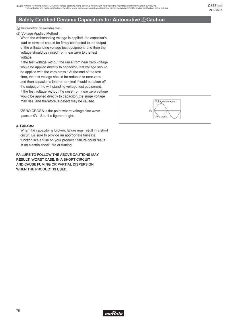
Safety Certifi ed Ceramic Capacitors for Automotive !Caution
Continued from the preceding page.
When the withstanding voltage is applied, the capacitor's lead or terminal should be firmly connected to the output of the withstanding voltage test equipment, and then the voltage should be raised from near zero to the test voltage.If the test voltage without the raise from near zero voltage would be applied directly to capacitor, test voltage should be applied with the zero cross.* At the end of the test time, the test voltage should be reduced to near zero, and then capacitor's lead or terminal should be taken off the output of the withstanding voltage test equipment.If the test voltage without the raise from near zero voltage would be applied directly to capacitor, the surge voltage may rise, and therefore, a defect may be caused.
*ZERO CROSS is the point where voltage sine wave passes 0V. See the figure at right.
(2) Voltage Applied Method
0V
zero cross
Voltage sine wave
When the capacitor is broken, failure may result in a short circuit. Be sure to provide an appropriate fail-safe function like a fuse on your product if failure could result in an electric shock, fire or fuming.
FAILURE TO FOLLOW THE ABOVE CAUTIONS MAY RESULT, WORST CASE, IN A SHORT CIRCUIT AND CAUSE FUMING OR PARTIAL DISPERSION WHEN THE PRODUCT IS USED.
4. Fail-Safe
C85E.pdfApr.7,2014
78
!Note • Please read rating and !CAUTION (for storage, operating, rating, soldering, mounting and handling) in this catalog to prevent smoking and/or burning, etc.• This catalog has only typical specifi cations. Therefore, please approve our product specifi cations or transact the approval sheet for product specifi cations before ordering.

Safety Certifi ed Ceramic Capacitors for Automotive !Caution
c !Caution (Storage and Operating Condition)
c !Caution (Soldering and Mounting)
c !Caution (Handling)
C85E.pdfApr.7,2014
79
!Note • Please read rating and !CAUTION (for storage, operating, rating, soldering, mounting and handling) in this catalog to prevent smoking and/or burning, etc.• This catalog has only typical specifi cations. Therefore, please approve our product specifi cations or transact the approval sheet for product specifi cations before ordering.
Operating and Storage Environment The insulating coating of capacitors does not form a perfect seal; therefore, do not use or store capacitors in a corrosive atmosphere, especially where chloride gas, sulfi de gas, acid, alkali, salt or the like are present. Also, avoid exposure to moisture. Before cleaning, bonding, or molding this product, verify that these processes do not affect product quality by testing the performance of a cleaned, bonded or molded product in the intended equipment. Store the capacitors where the temperature and relative humidity do not exceed -10 to 40 degrees centigrade and 15 to 85%.
Use capacitors within 6 months after delivery. Check the solderability after 6 months or more. FAILURE TO FOLLOW THE ABOVE CAUTIONS MAY RESULT, WORST CASE, IN A SHORT CIRCUIT AND CAUSE FUMING OR PARTIAL DISPERSION WHEN THE PRODUCT IS USED.
1. Vibration and Impact Do not expose a capacitor or its lead wires to excessive shock or vibration during use. Excessive shock or vibration may cause fatigue destruction of lead wires mounted on the circuit board. Please take measures to hold a capacitor on the circuit boards by adhesive, molding resin or another coating. Please confi rm there is no infl uence of holding measures on the product with the intended equipment.2. Soldering When soldering this product to a PCB/PWB, do not exceed the solder heat resistance specifi cations of the capacitor. Subjecting this product to excessive heating could melt the internal junction solder and may result in thermal shocks that can crack the ceramic element. Soldering the capacitor with a soldering iron should be performed in the following conditions. Temperature of iron-tip: 400 degrees C. max. Soldering iron wattage: 50W max. Soldering time: 3.5 sec. max.
3. Bonding, Resin Molding and Coating For bonding, molding or coating this product, verify that these processes do not affect the quality of the capacitor by testing the performance of the bonded, molded or coated product in the intended equipment. When the amount of applications, dryness/hardening conditions of adhesives and molding resins containing organic solvents (ethyl acetate, methyl ethyl ketone, toluene, etc). are unsuitable, the outer coating resin of a capacitor is damaged by the organic solvents and it may result, worst case, in a short circuit. The variation in thickness of adhesive, molding resin or coating may cause outer coating resin cracking and/or ceramic element cracking of a capacitor in a temperature cycling.4. Treatment after Bonding, Resin Molding and Coating When the outer coating is hot (over 100 degrees C.) after soldering, it becomes soft and fragile. Therefore, please be careful not to give it mechanical stress. FAILURE TO FOLLOW THE ABOVE CAUTIONS MAY RESULT, WORST CASE, IN A SHORT CIRCUIT AND CAUSE FUMING OR PARTIAL DISPERSION WHEN THE PRODUCT IS USED.
Vibration and Impact Do not expose a capacitor or its lead wires to excessive shock or vibration during use. Excessive shock or vibration may cause fatigue destruction of lead wires mounted on the circuit board. Please take measures to hold a capacitor on the circuit boards by adhesive, molding resin or another coating.
Please confi rm there is no infl uence of holding measures on the product with the intended equipment. FAILURE TO FOLLOW THE ABOVE CAUTIONS MAY RESULT, WORST CASE, IN A SHORT CIRCUIT AND CAUSE FUMING OR PARTIAL DISPERSION WHEN THE PRODUCT IS USED.
Safety Certifi ed Ceramic Capacitors for Automotive Notice
c Notice (Soldering and Mounting)Cleaning (ultrasonic cleaning) To perform ultrasonic cleaning, observe the following conditions. Rinse bath capacity: Output of 20 watts per liter or less. Rinsing time: 5 min. maximum. Do not vibrate the PCB/PWB directly. Excessive ultrasonic cleaning may lead to fatigue destruction of the lead wires.
c Notice (Rating)1. Capacitance Change of Capacitors Capacitors have an aging characteristic, whereby the capacitor continually decreases its capacitance slightly if the capacitor is left on for a long time. Moreover, capacitance might change greatly depending on the surrounding temperature or an applied voltage. Therefore, it is not likely to be suitable for use in a constant time circuit. Please contact us if you need detailed information.2. Performance Check by Equipment Before using a capacitor, check that there is no problem in the equipment's performance and the specifi cations.
Generally speaking, CLASS 2 ceramic capacitors have voltage dependence characteristics and temperature dependence characteristics in capacitance. Therefore, the capacitance value may change depending on the operating condition in the equipment. Therefore, be sure to confi rm the apparatus performance of receiving infl uence in the capacitance value change of a capacitor, such as leakage current and noise suppression characteristic. Moreover, check the surge-proof ability of a capacitor in the equipment, if needed, because the surge voltage may exceed specifi c value by the inductance of the circuit.
C85E.pdfApr.7,2014
80
!Note • Please read rating and !CAUTION (for storage, operating, rating, soldering, mounting and handling) in this catalog to prevent smoking and/or burning, etc.• This catalog has only typical specifi cations. Therefore, please approve our product specifi cations or transact the approval sheet for product specifi cations before ordering.
Safety Certifi ed Ceramic Capacitors/High Voltage Ceramic Capacitors ISO9000 Certifi cations
Plant Applied Standard
ISO9001Izumo Murata Manufacturing Co., Ltd.
Taiwan Murata Electronics Co., Ltd.
ISO9001Murata Electronics (Thailand), Ltd.
ISO9001
Manufacturing plants that produce the products in this catalog have obtained the ISO9000 quality system certificate.
C85E.pdfApr.7,2014
81
!Note • Please read rating and !CAUTION (for storage, operating, rating, soldering, mounting and handling) in this catalog to prevent smoking and/or burning, etc.• This catalog has only typical specifi cations. Therefore, please approve our product specifi cations or transact the approval sheet for product specifi cations before ordering.

!Note C85E.pdfApr.7,2014
• Please read rating and !CAUTION (for storage, operating, rating, soldering, mounting and handling) in this catalog to prevent smoking and/or burning, etc.• This catalog has only typical specifi cations. Therefore, please approve our product specifi cations or transact the approval sheet for product specifi cations before ordering.


