SYNTHESIS AND PHOTOPHYSICAL STUDIES OF
BIPOLAR HOST MATERIALS FOR
PHOSPHORESCENT OLEDS
Submitted for partial fulfilment for
Master of Science in chemistry
By
Suraj Kumar Panigrahi
Under the guidance of
Prof. Vaidyanathan Sivakumar
Department of chemistry,
National Institute of Technology,
Rourkela-769008, Odisha
May 2014
2
Certificate
This is to certify that the project report entitled, “Synthesis and Photophysical studies of
Bipolar host materials for Phosphorescent OLEDs”, is being submitted to National
Institute Technology, Rourkela by Mr SURAJ KUMAR PANIGRAHI having roll number
412cy2019 for partial fulfilment of the Master of Science degree, Chemistry, which is an
original work carried out under my guidance and supervision. This work has not been
submitted by him to any other University or Institute.
The present study is a valuable contribution for the advancement of knowledge in the field of
Optoelectronics and lightening Industry.
In habit and character Mr SURAJ KUMAR PANIGRAHI is quite a fit and proper person for
the further research work.
I wish him all success in his future life.
Date:
Prof. V.Sivakumar
Department Of Chemistry
NIT- Rourkela

3
DECLARATION
I Suraj Kumar Panigrahi hereby declare that this project report entitled “Development of non-
conjugated bipolar hybrid hosts for organic phosphorescent light-emitting diodes” is the
original work carried out by me under the supervision of Dr. V.Sivakumar, Department Of
Chemistry, National Institute of Technology, Rourkela (Odisha) and the present work or any
other part thereof has not been presented to any other University and Institution for the award
of any other degree regarding to my belief.
Suraj Kumar Panigrahi
412CY2019

4
ACKNOWLEDGEMENTS
I wish to express my deep sense of gratitude and indebtedness to Prof. V. Sivakumar
Department of Chemistry, N.I.T Rourkela for assigning me in the project and for his inspiring
guidance, constructive criticism and valuable suggestion throughout this project work.
I express my heartfelt thanks to Dr. N. Panda, HOD, Department of Chemistry, NIT, and all
other esteemed Professors of Chemistry department of NIT Rourkela for their valuable
suggestions and encouragements at various stages of the work.
I extend my heartiest gratitude to Mr. Arvind kajjam for extending the maximum possible
support and helping me during my whole project work, without the help of Mr. Arvind
kajjam this project seems to be incomplete.
I am also thankful to Mr. Rajamouli Boddula, Mrs. Kasturi Singh for constantly encouraging
me and guiding me throughout this project and providing all joyful environments in the lab.
Last but not the least, I sincerely thank to all my friends who have patently extended all sorts
of help for accomplishing this undertaking.
Suraj Kumar Panigrahi
5
Abstract
The remarkable progress of light-emitting organic semiconductors has led to the
establishment of organic light-emitting diodes (OLEDs) as a major display technology.
Furthermore, it has opened new directions for materials and devices, and exciting new
applications. In the present work, three efficient organic green to yellow emitting bipolar
materials, 3-(4-(diphenylamino)phenyl)-1-phenylprop-2-en-1-one (DPPO), 3-(4-(9H-
carbazol-9-yl)phenyl)-1-phenylprop-2-en-1-one (CPPO) and 4-(bis(4-
(diphenylamino)phenyl)amino) )-1-phenylprop-2-en-1-one (BDPPO) were synthesized. The
bipolar materials were characterized by 1H NMR,
13C NMR, Mass, UV-Visible, TGA-DTA
and PL spectroscopy techniques. The synthesized phosphor materials are emitting green to
yellow color with good emission intensity and can be used in the white light emitting LEDs.

6
ABBREVIATIONS
Alq3………………………... tris-(8-hydroxyquinoline )aluminium
CV …………………………. Cyclic voltammetry
DCM ……………………..... Dichloromethane
ECHB ……………………… Electron-conducting I hole-blocking
EL …………………………. Electro luminescence
ET ………………………………………… Triplet energy
EQE ……………………….. External quantum efficiency
HOMO …………………...... Highest occupied molecular orbital
LUMO …………………….. Lowest unoccupied molecular orbital
ITO ………………………… Indium tin oxide
MEH-PPV ………………… poly[2-(2'-ethylhexyloxy)-5-methoxy-1,4-
phenylenevinylene]
Mp …………………………. Melting point
NEt3 …………………………………….. Triethylamine
NMR ………………………. Nuclear magnetic resonance
OLEDs …………………….. Organic light-emitting devices
PBD ……………………….. 5-( 4-biphenyl)-2-( 4-tert-butylphenyl)-1 ,3,4-oxadiazole
PEDOT ……………………. poly( ethylenedioxy-thiophene)
PET ………………………... poly( ethyleneterphthalate)
PL ………………………….. Photoluminescence
PPV ………………………... poly(p-phenylenevinylene)
Ppy ………………………… poly(pyridine-2,5-diyl)
PPym ………………………. poly(pyrimidine-2,5-diyl)
PVK ……………………….. poly(vinylcarbazole) 32
TIPD ………………………. 2,2 ',2"-(1 ,3,5-benzenetriyl)tris{l-phenyl)-1 H-benzimidazole
Tg ………………………….. Glass transition temperature
THF ………………………... Tetrahydro furan
TLC ………………………... Thin layer chromatography
Uv …………………………. Ultraviolet
Vis …………………………. Visible

7
S.No Table of Content Page No
Abstract 5
Abbreviations 6
1 Chapter-1 – Background and Introduction
1.1. Luminescence ………………………………………... 8
1.1.1. Photoluminescence …………………………... 8
1.1.2. Electroluminescence …………………………. 8
1.1.2.1. Organic electroluminescence …….. 9
1.2. Organic material ……………………………………… 11
1.2.1. Fluorescent emitters ………………………….. 11
1.2.2. Phosphorescent emitters ……………………... 12
2 Chapter-2 – Bipolar hosts for phosphorescent OLEDs
2.1 An overview of phosphorescent OLEDs …………….. 13
2.2 Typical hole transport material ………………………. 16
2.3 Electron transport type material ……………………… 17
2.4 Bipolar transport type material ………………………. 18
2.5 Molecular design of bipolar transport type host ……... 18
2.6 Objective of present study …………………………… 20
3 Chapter-3 – Experimental section
3.1 Material synthesis ……………………………………. 20
3.2 Instruments and photophysical characterizations ……. 24
4 Chapter-4 - Results and discussion
4.1. UV-Vis data………………………………………….. 25
4.2. Mass Spectra…………………………………………. 26
4.3. TGA-DTA…………………………………………… 27
4.4. Fluorescence…………………………………………. 19
5 Chapter-5 – Conclusion
5.1. Summary ……………………………………………... 30
5.2. Future study ………………………………………….. 30
6 Chapter-6- References ……………………………………………… 31
8
Chapter 1
Background and Introduction
1.1. Luminescence:
Luminescence is the production of light from a compound (either organic or inorganic).
Luminescence can occur following a number of different mechanisms. Organic compounds
suitable for OLED applications will display photoluminescence and electroluminescence.
In order for a material to emit energy in the form of light energy it needs to be in a higher
energy (excited) state which can come back to the ground state by releasing energy in the
form of a photon or through a nonradiative pathway. These excited states can be formed by
photoexcitation (photoluminescence) or electronic excitation (electroluminescence).
1.1.1. Photoluminescence:
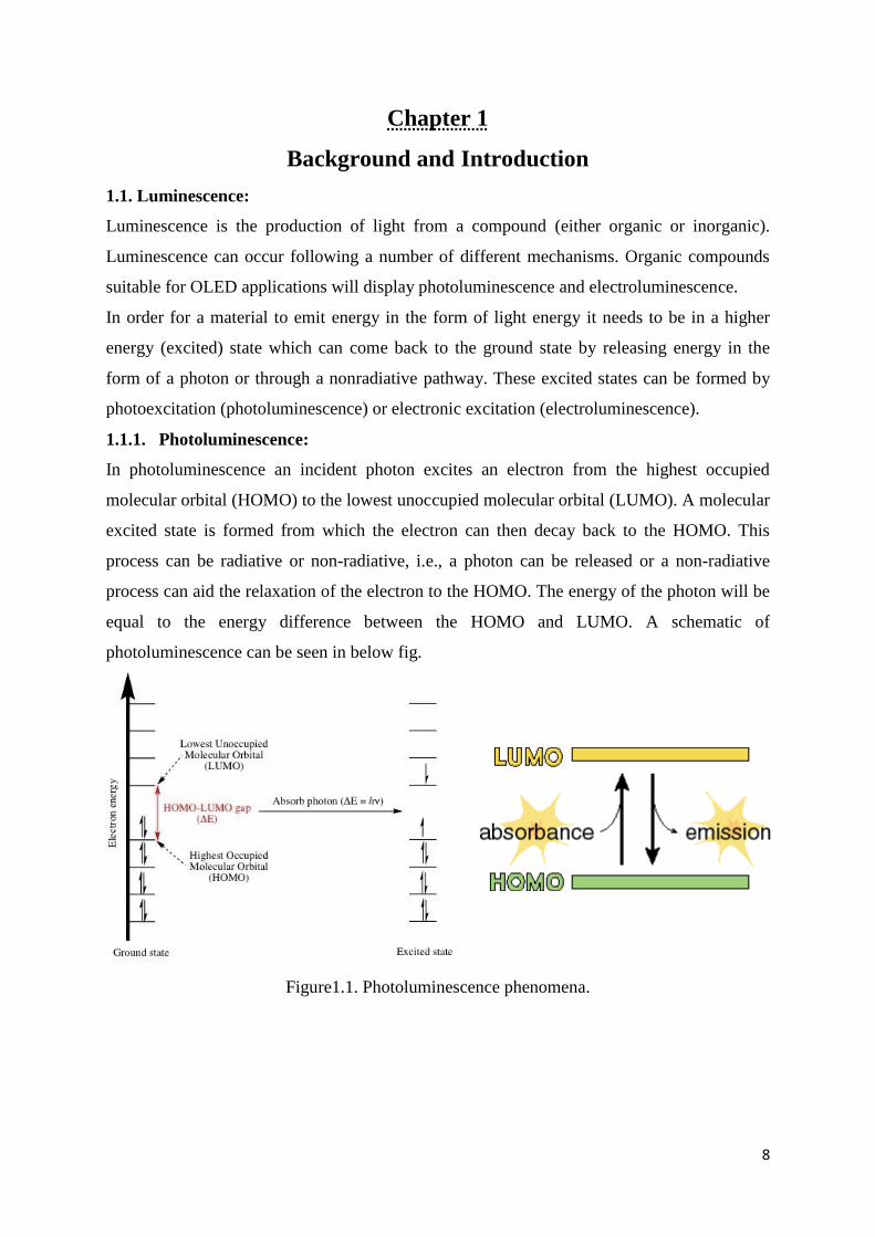
In photoluminescence an incident photon excites an electron from the highest occupied
molecular orbital (HOMO) to the lowest unoccupied molecular orbital (LUMO). A molecular
excited state is formed from which the electron can then decay back to the HOMO. This
process can be radiative or non-radiative, i.e., a photon can be released or a non-radiative
process can aid the relaxation of the electron to the HOMO. The energy of the photon will be
equal to the energy difference between the HOMO and LUMO. A schematic of
photoluminescence can be seen in below fig.
Figure1.1. Photoluminescence phenomena.
9
1.1.2. Electroluminescence:
Electroluminescence can be defined as the production of light from a material when an
electric field is applied across it. It requires the excitation of the material into a higher energy
state which can occur through various mechanisms and the subsequent relaxation of the
material to a lower energy state resulting in the release of a photon. Long before organic
materials were thought of as potential electroluminescent materials inorganic semiconductors
were being used in light emitting diodes –LEDs The first example of electroluminescence
was reported over 100 years ago[1]
in a note to the editors of Electrical World. It was found
that when a potential difference was applied across a crystal of carborundum (silicon carbide)
a yellowish light was produced. Unfortunately, the discovery was not followed up and it was
not until the mid-1920s that the LED was‘re-invented'[2]
.
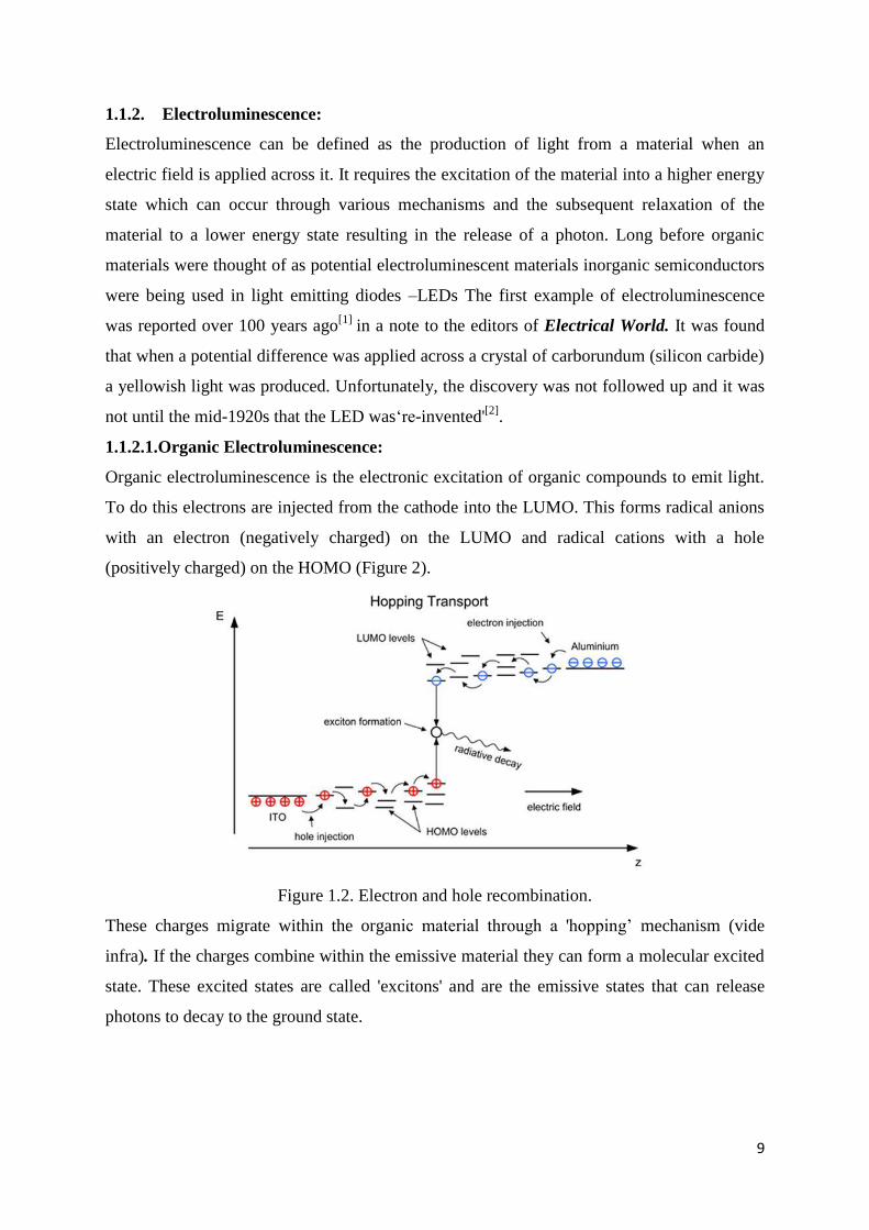
1.1.2.1.Organic Electroluminescence:
Organic electroluminescence is the electronic excitation of organic compounds to emit light.
To do this electrons are injected from the cathode into the LUMO. This forms radical anions
with an electron (negatively charged) on the LUMO and radical cations with a hole
(positively charged) on the HOMO (Figure 2).
Figure 1.2. Electron and hole recombination.
These charges migrate within the organic material through a 'hopping’ mechanism (vide
infra). If the charges combine within the emissive material they can form a molecular excited
state. These excited states are called 'excitons' and are the emissive states that can release
photons to decay to the ground state.
10
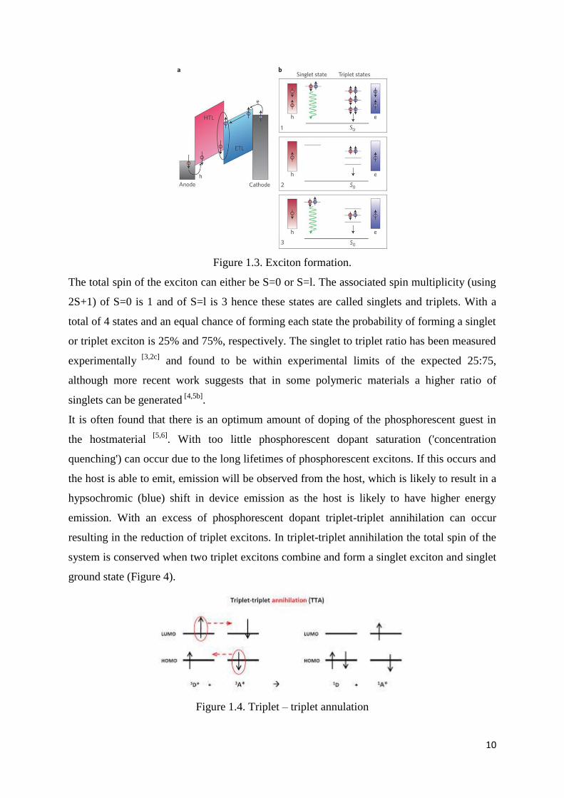
Figure 1.3. Exciton formation.
The total spin of the exciton can either be S=0 or S=l. The associated spin multiplicity (using
2S+1) of S=0 is 1 and of S=l is 3 hence these states are called singlets and triplets. With a
total of 4 states and an equal chance of forming each state the probability of forming a singlet
or triplet exciton is 25% and 75%, respectively. The singlet to triplet ratio has been measured
experimentally [3,2c]
and found to be within experimental limits of the expected 25:75,
although more recent work suggests that in some polymeric materials a higher ratio of
singlets can be generated [4,5b]
.
It is often found that there is an optimum amount of doping of the phosphorescent guest in
the hostmaterial [5,6]
. With too little phosphorescent dopant saturation ('concentration
quenching') can occur due to the long lifetimes of phosphorescent excitons. If this occurs and
the host is able to emit, emission will be observed from the host, which is likely to result in a
hypsochromic (blue) shift in device emission as the host is likely to have higher energy
emission. With an excess of phosphorescent dopant triplet-triplet annihilation can occur
resulting in the reduction of triplet excitons. In triplet-triplet annihilation the total spin of the
system is conserved when two triplet excitons combine and form a singlet exciton and singlet
ground state (Figure 4).
Figure 1.4. Triplet – triplet annulation

11
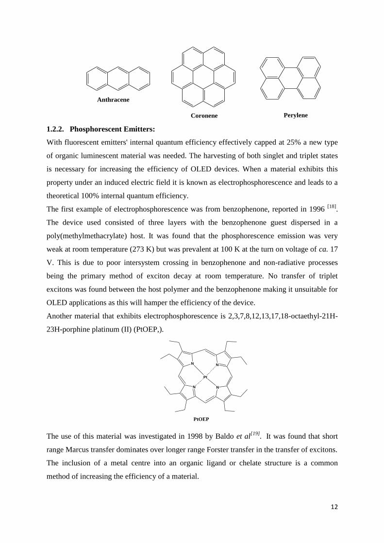
1.2. Organic Materials:
Organic Materials can either be small molecule or polymeric. Here the focus directed to small
molecules. Fluorescent polymer light emitting devices, PLEDs, have had a huge impact in the
field of OLEDs since the discovery of electroluminescence in a poly(phenylenevinylene)
(PPV) derivative[7]
.
Small molecule organic materials for LEDs can be classified into two families - fluorescent
and phosphorescent emitters.
1.2.1. Fluorescent Emitters:
Although singlet and triplet excitons were expected to be formed through charge
recombination, only the singlet states were emitting, noting that the triplet states were
expected to decay through a non-radiative pathway.
In 1987 Tang and VanSlyke published a revolutionary paper[9]
describing a two layer device
of a metal chelate complex (Alq3) as the electron transporting and emitting layer and a
diamine (TAPC) as the hole transporting layer. The inclusion of these transporting layers was
found to greatly improve the efficiency of the device. The device structure is shown in the
following figure 5.
Ca-Ag
Alq3
(Diamine)TAPC
ITO
Glass
Figure 1.5. Device structure of two layer metal chelate complex
The advances in 1987 spurned on efforts to create new hole- and electron-transporting
materials to improve device performance. Adachi and co-workers [10]
developed a three layer
device utilising an aromatic diamine (TPD) as the HTL and a perylene tetracarboxylic acid
derivative (PV) as the ETL. Anthracene, coronene and perylene (depicted below) were
chosen as the emissive materials as they fluoresce with different colours.
In 1989 Tang, VanSlyke and Chen [11]
published a novel device structure based on their
original two layer device. This new structure used a fluorescent dopant in the Alq3 layer
giving a device structure of ITO/diamine/Alq3 (3)/doped Alq3/Alq3 (3)/Mg:Ag.
12
Anthracene
Coronene Perylene
1.2.2. Phosphorescent Emitters:
With fluorescent emitters' internal quantum efficiency effectively capped at 25% a new type
of organic luminescent material was needed. The harvesting of both singlet and triplet states
is necessary for increasing the efficiency of OLED devices. When a material exhibits this
property under an induced electric field it is known as electrophosphorescence and leads to a
theoretical 100% internal quantum efficiency.
The first example of electrophosphorescence was from benzophenone, reported in 1996 [18]
.
The device used consisted of three layers with the benzophenone guest dispersed in a
poly(methylmethacrylate) host. It was found that the phosphorescence emission was very
weak at room temperature (273 K) but was prevalent at 100 K at the turn on voltage of ca. 17
V. This is due to poor intersystem crossing in benzophenone and non-radiative processes
being the primary method of exciton decay at room temperature. No transfer of triplet
excitons was found between the host polymer and the benzophenone making it unsuitable for
OLED applications as this will hamper the efficiency of the device.
Another material that exhibits electrophosphorescence is 2,3,7,8,12,13,17,18-octaethyl-21H-
23H-porphine platinum (II) (PtOEP,).
The use of this material was investigated in 1998 by Baldo et al[19]
. It was found that short
range Marcus transfer dominates over longer range Forster transfer in the transfer of excitons.
The inclusion of a metal centre into an organic ligand or chelate structure is a common
method of increasing the efficiency of a material.
N
Pt
N
N N
PtOEP
13
Chapter 2
Bipolar Hosts for Phosphorescent OLEDs
2.1. An overview of PhOLEDs
Since the invention of relatively efficient fluorescent organic light-emitting diodes (OLEDs)
in 1987, [13]
a new generation of flat-panel displays has emerged with a potential for capturing
a substantial market share of consumable electronics, such as television sets and computer
monitors. While full-color OLED displays require the emission of blue, green and red light,
white OLEDs are potentially useful for efficient and inexpensive solid-state lighting and as
backlights for liquid crystal displays. [14-16]
Compared to molecular materials that can be
vacuum-deposited into thin films, solution-processable materials, such as π-conjugated
polymers and monodisperse oligomers, offer cost advantage and ease of scale-up to large-
area thin films. Fluorescence or phosphorescence is responsible for light emission from
organic luminophores. Electrophosphorescence is superior to electrofluorescence in terms of
readily accessible internal quantum yield, 100 versus 25 %. Despite the intensive efforts
worldwide over the past decade, device efficiency and lifetime have remained critical issues.
For the fabrication of an efficient phosphorescent OLED, a triplet emitter is typically doped
in a host material with sufficiently high triplet energy, ET, to realize blue, green or red
emission. [17-20]
A higher ET of the host than the guest ensures exciton transfer from the
former to the latter where light emission occurs. In cases where the triplet emitters serve as
charge traps, exciton formation is expected at the emitter without back-transfer to the host
because of the higher ET of the latter. Compared to exciton transfer from the host, charge
trapping on the emitter as the source of phosphorescence is advantageous in terms of the
higher internal quantum yield, [18, 21, 22]
less concentration quenching because of the lower
doping level, [21, 23]
and the emission spectrum solely from the emitter, [23, 24]
albeit at the
higher driving voltage.[24]
Most of the existing triplet host materials are capable of preferentially transporting holes or
electrons. [19, 25, 26]
Charge injection and transport layers are added between electrodes and the
emitting layer as needed to improve efficiency. [17-20, 25, 27]
Nevertheless, charge
recombination tends to occur close to the interface with the charge-transport layer for lack of
bipolar transport capability in general of the emitting layer. [28, 29]
Under a high current
density pertaining to practical application, confinement of excitons to the interfacial region
could expedite triplet-triplet annihilation, resulting in efficiency roll-off. [30-33]
Furthermore, a
narrow recombination zone is detrimental to operational stability because only a fraction of

14
molecules contribute to charge transport, exciton formation, and light emission. [34-36]
to
substantially improve device efficiency and lifetime, it is imperative that excitons be evenly
distributed through the emitting layer and that the accumulation of charges and excitons at
interfaces be prevented. To this effect, it has been demonstrated that mixed hosts can
effectively decrease driving voltage while improving device efficiency sustainable at high
current densities. [23, 24, 37-42]
A typical phosphorescent layer is comprised of a host mixed with
a charge-transport component at 25 to 50 wt%, to which 1 to 10 wt% of a triplet emitter is
doped. The desired bipolar transport capability entails a high concentration of the charge-
transport additive, at which doping level phase separation is destined to take place over time
unless miscibility has been taken into account in the design of both components, thus
adversely affecting long-term operational stability of OLEDs. Bipolar charge-transport host
materials via chemical modification represent a viable approach to circumventing the
potential phase-separation problem.
Generally, in these host/guest (dopant) systems, three roots can lead to dopant emission as
shown in the following figure 6. [25-26]
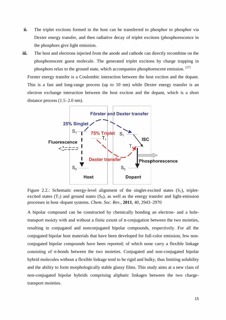
Figure 2.1.: Schematic representation of Forster energy transfer (a) and Dexter energy
transfer (b); energy transfer (c) and charge trapping (d) alignment for dopant emission in
host–dopant systems. Chem. Soc. Rev., 2011, 40, 2943–2970
i. The singlet excitons formed in the host under electrical excitation can be transferred to
phosphor via Forster and Dexter energy transfer, and then singlet excitons in the phosphor
are converted to triplet excitons by efficient intersystem crossing.
15
ii. The triplet excitons formed in the host can be transferred to phosphor to phosphor via
Dexter energy transfer, and then radiative decay of triplet excitons (phosphorescence in
the phosphors give light emission.
iii. The host and electrons injected from the anode and cathode can directly recombine on the
phosphorescent guest molecule. The generated triplet excitons by charge trapping in
phosphors relax to the ground state, which accompanies phosphorescent emission. [27]
Forster energy transfer is a Coulombic interaction between the host exciton and the dopant.
This is a fast and long-range process (up to 10 nm) while Dexter energy transfer is an
electron exchange interaction between the host exciton and the dopant, which is a short
distance process (1.5–2.0 nm).
Figure 2.2.: Schematic energy-level alignment of the singlet-excited states (S1), triplet-
excited states (T1) and ground states (S0), as well as the energy transfer and light-emission
processes in host–dopant systems. Chem. Soc. Rev., 2011, 40, 2943–2970
A bipolar compound can be constructed by chemically bonding an electron- and a hole-
transport moiety with and without a finite extent of π-conjugation between the two moieties,
resulting in conjugated and nonconjugated bipolar compounds, respectively. For all the
conjugated bipolar host materials that have been developed for full-color emission, few non-
conjugated bipolar compounds have been reported; of which none carry a flexible linkage
consisting of σ-bonds between the two moieties. Conjugated and non-conjugated bipolar
hybrid molecules without a flexible linkage tend to be rigid and bulky, thus limiting solubility
and the ability to form morphologically stable glassy films. This study aims at a new class of
non-conjugated bipolar hybrids comprising aliphatic linkages between the two charge-
transport moieties.

16
To achieve efficient electro phosphorescence, the development of effective host materials is
of importance. In the search for novel host materials for phosphorescent OLEDs, several
requirements have to be considered. [29-32]
The hosts should possess higher triplet energies than those of the dopant emitters to
prevent reverse energy transfer from the guest back to the host, as well as confine
triplet excitons in the emissive layer.
The highest occupied molecular orbitals (HOMOs) and the lowest unoccupied
molecular orbitals (LUMOs) of host materials should match with those of
neighbouring active layers to reduce the hole and electron injection barrier, thus
lowering the device driving voltages.
The hosts are expected to have good and balanced charge carrier transport properties
for the hole–electron recombination process and confinement of the exciton formation
zone in the emissive layer.
The host materials should have good thermal and morphological stability, which
could reduce the possibility of phase separation upon heating, thus prolonging the
device operational lifetime. Generally, a bulky and sterically hindered molecular
configuration is preferable to enhance the glass transition temperature (Tg) and form
morphologically stable and uniform amorphous films.
2.2. Typical hole transport materials
The molecular structure of hole transporting materials contain electron-donating moieties.
Common examples are triphenylamine (TPA), diphenylamine, carbazole etc. a good hole
transporting material should possess i. Good hole mobility, ii. A high glass transition
temperature (Tg) to form morphologically and thermally stable thin film, iii. A proper
HOMO level to confirm a low energy barrier for hole injection from anode and then to the
emissive layer. iv. A suitable LUMO level to block electron injection from the emissive layer
(EML) to the hole transporting layer (HTL), v. High triplet energy to confine triplet excitons
in the EML.

17
2.3. Electron transport type host materials
The electron transport type host materials basically contain electron withdrawing groups in
their molecular structure and primarily transport electrons. In contrast to hole transporting
host materials, electron transporting host materials are rare. Alq3 was the first used electron
transporting host material in the initial work of electrophosphorescence. however its low
triplet energy of 2.0 eV hinders its application. It can only act as a host for deep red to near
IR emitters. In order to broaden the recombination zone and balance the charge in EML,
TPBI is generally used as electron transport type host in a mixed host system or double
emissive layer. [26, 27, 28]
Electron transport type host materials are beneficial to achieve charge balance in
electrophosphorescent devices. A desired electron transport type host material should have
high triplet energy to prevent reverse energy transfer from the guest back to the host, normal
thermal stability to form morphologically stable and uniform amorphous films, low electron
injection barriers to reduce the driving voltage.
Various electron-transport type host materials are as follows:
N N
Biphen
Aluminium tris(8-hydroxyquinoline)
N
N
N
AlO O
O
N N
O
PBD
Si
N
N
N
DTBT
NN
TPDNPB
N
NN
N
TCTA
N
N
TAPC
18
2.4. Bipolar transport host materials
Most of the previously reported host materials are effectively capable of transporting holes
and electrons. The recombination zone tends to occur close to the EML/ETL interface when
using hole transport host. Similarly the recombination zone tend to occur at the EML/HTL
interface when using an electron transport host.[30]
the poor carrier mobility and unbalanced
charges in the emitting layer have been proven to be due to the efficiency of OLEDs.
PhOLEDs with narrow charge recombination zone could undergo triplet-triplet annihilation,
which results in efficiency roll off due to a local accumulation of high density of triplet
excitons, especially under high current densities.[25]
hence the strategy of using double
emissive layers with hole or electron transporting host in each emissive layer with both hole
and electron transporting hosts have been presented to broaden the recombination zone and
improve the device efficiency. [27, 28, 29]
the two strategies make the fabrication of the device
complicated. Also the mixed host may cause a potential phase separation problems. Hence to
achieve highly efficient electrophosphorescence, host materials with balanced charge
transport feature to generate broad charge recombination zones in the emissive layer are
preferable.
Bipolar host materials have got great attention in the field of phosphorescent OLEDs because
of their ability to provide more balance in electron and hole fluxes and simplify device
structure. They have also extraordinarily high efficiency.
2.5. Molecular design of bipolar host materials
A suitable bipolar host in PhOLEDs must have some basic requirements.
i. Bipolarity to facilitate both hole and electron injection and transport. Bipolar compounds
should have both electron-donating (comprised of arylamines such as carbazole,
diphenylamine, triphenylamine etc.) and electron-withdrawing (consists of phenanthroline,
oxadiazole, triazole, benzoimidazole, pyridine, phosphine oxide, triazine and so on) groups.
ii. Good morphological and thermal stability to ensure device stability. iii. Matching HOMO
and LUMO layers with those of the adjacent layers to reduce charge injection barriers and
device driving voltage. iv. Higher triplet energy than the dopant to effectively prevent
exothermic reverse energy transfer from the guest emitter to the host moiety.
However it is difficult for a bipolar host to achieve higher triplet energy because the electron
withdrawing and hole transporting moieties in one molecule lowers the band gap of the
material through intermolecular charge transfer, while the low triplet energy of the host can
cause reverse energy transfer, which results in the decreased efficiency of PhOLEDs. To
19
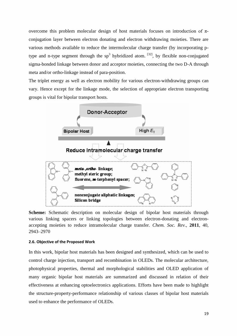
overcome this problem molecular design of host materials focuses on introduction of π-
conjugation layer between electron donating and electron withdrawing moieties. There are
various methods available to reduce the intermolecular charge transfer (by incorporating p-
type and n-type segment through the sp3 hybridized atom.
[32], by flexible non-conjugated
sigma-bonded linkage between donor and acceptor moieties, connecting the two D-A through
meta and/or ortho-linkage instead of para-position.
The triplet energy as well as electron mobility for various electron-withdrawing groups can
vary. Hence except for the linkage mode, the selection of appropriate electron transporting
groups is vital for bipolar transport hosts.
Scheme: Schematic description on molecular design of bipolar host materials through
various linking spacers or linking topologies between electron-donating and electron-
accepting moieties to reduce intramolecular charge transfer. Chem. Soc. Rev., 2011, 40,
2943–2970
2.6. Objective of the Proposed Work
In this work, bipolar host materials has been designed and synthesized, which can be used to
control charge injection, transport and recombination in OLEDs. The molecular architecture,
photophysical properties, thermal and morphological stabilities and OLED application of
many organic bipolar host materials are summarized and discussed in relation of their
effectiveness at enhancing optoelectronics applications. Efforts have been made to highlight
the structure-property-performance relationship of various classes of bipolar host materials
used to enhance the performance of OLEDs.

20
Chapter 3
EXPERIMENTAL SECTION
3.2 Experimental
Material Synthesis
All chemicals, reagents, solvents were used as received from commercial sources without
further purification except toluene, tetrahydrofuran (THF) and chloroform (CHCl3) that had
been distilled over sodium, benzophenone and P2O5 respectively. Those reactions which are
moisture sensitive were carried out under nitrogen and anhydrous conditions unless noted
otherwise. 1H NMR spectra were acquired in CDCl3 with an Advance-400 spectrometer (400
MHz) at 298 K using trimethylsilane (TMS) as an internal standard. Elemental analysis was
carried out by Quantitative Technologies, Inc. Molecular weights were measured with an ESI
Mass spectrometer (Perkin Elmer, USA). The target compounds were synthesized and
purified according to reaction Scheme 1-3 following the procedures described below.
O H
O
a
Scheme 1: Reagents and Conditions: a= C6H5OH, NaOH, C2H5OH, H2O;
Scheme 2: Reagents and Conditions: b=POCl3, DMF, 00C, CHCl3, 100
0C; c= C6H5OH,
NaOH, C2H5OH, H2O;
N
N
O H
N
O
b c
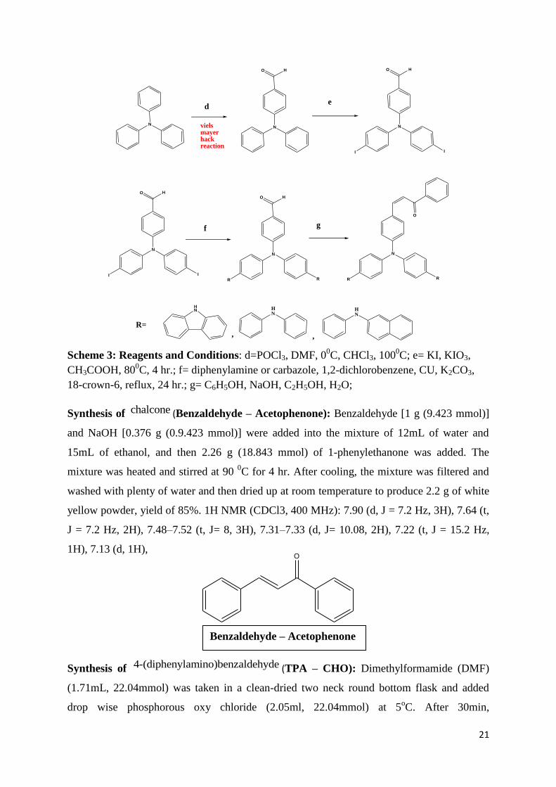
21
NN N
II
N
II
N
RR
R=
HN H
NHN
e
f
viels mayer hack reaction
N
RR
O
g
, ,
d
O H O H
O HO H
Scheme 3: Reagents and Conditions: d=POCl3, DMF, 00C, CHCl3, 100
0C; e= KI, KIO3,
CH3COOH, 800C, 4 hr.; f= diphenylamine or carbazole, 1,2-dichlorobenzene, CU, K2CO3,
18-crown-6, reflux, 24 hr.; g= C6H5OH, NaOH, C2H5OH, H2O;
Synthesis of chalcone (Benzaldehyde – Acetophenone): Benzaldehyde [1 g (9.423 mmol)]
and NaOH [0.376 g (0.9.423 mmol)] were added into the mixture of 12mL of water and
15mL of ethanol, and then 2.26 g (18.843 mmol) of 1-phenylethanone was added. The
mixture was heated and stirred at 90 0C for 4 hr. After cooling, the mixture was filtered and
washed with plenty of water and then dried up at room temperature to produce 2.2 g of white
yellow powder, yield of 85%. 1H NMR (CDCl3, 400 MHz): 7.90 (d, J = 7.2 Hz, 3H), 7.64 (t,
J = 7.2 Hz, 2H), 7.48–7.52 (t, J= 8, 3H), 7.31–7.33 (d, J= 10.08, 2H), 7.22 (t, J = 15.2 Hz,
1H), 7.13 (d, 1H),
Synthesis of 4-(diphenylamino)benzaldehyde (TPA – CHO): Dimethylformamide (DMF)
(1.71mL, 22.04mmol) was taken in a clean-dried two neck round bottom flask and added
drop wise phosphorous oxy chloride (2.05ml, 22.04mmol) at 5oC. After 30min,
O
Benzaldehyde – Acetophenone

22
triphenylamine (TPA) (2g, 8.163mmol) in DMF (15mL) was added drop wise to reaction
mixture at same temperature. The resulting mixture was stirred for overnight at RT, then
poured into water and neutralized with diluted sodium hydroxide solution (up to pH 6). Then
extracted with chloroform and washed with brine solution followed by dried with sodium
sulphate. The crude product was washed with diethyl ether: hexane (3:7) mixture solvent and
recrystallization in ethanol to get 2g pure 4-1 (90%) with pale yellow colored fine solid.1H-
NMR Data (CdCl3, 400MHz): 9.82 (s, 1H), 7.70 (d, 2H), 7.38-7.34 (m, 2H), 7.25-7.24 (m,
2H), 7.20-7.15 (m, 6H), 7.03 (d, 2H). 13
C-NMR Data (CdCl3, 100MHz): 153.3, 146.1,
131.3, 129.7, 129.0, 126.3, 125.1, 119.3.
Synthesis of (Z)-3-(4-(diphenylamino)phenyl)-1-phenylprop-2-en-1-one (TPA-
Acetophenone): TPA-CHO [0.5 g (1.831 mmol)] and NaOH [0.08 g (1.831 mmol)] were
added into the mixture of 30mL of water and 25mL of ethanol, then 0.24 g (3.663 mmol) of
1-phenylethanone was added. The mixture was heated and stirred at 90 0C for 4 hr. After
cooling, the mixture was filtered and washed with plenty of water and then dried up at room
temperature to produce 0.3 g of yellow powder, yield of 80%. 1H NMR (CDCl3, 400 MHz):
8.01 (d, J = 7.5 Hz, 2H), 7.77 (d, J = 16.0 Hz, 1H), 7.58–7.54 (t, 1H), 7.51–7.48 (m, 4H), 7.39
(d, J = 16.0 Hz, 1H), 7.34–7.29 (m, 4H), 7.18–7.09 (m, 6H), 7.03 (d, J = 8.0 Hz, 2H).
N
O
N N
CHO
POCl3
DMF, RT
TPA-Acetophenone
TPA – CHO
23
Synthesis of 4-(bis(4-iodophenyl)amino)benzaldehyde (TPA – CHO –I2): Under rapid
stirring, 4 (2.73 g, 10 mmol) was dissolved in glacial acetic acid (10 mL) and KI (3.32 g, 20
mmol) and KIO3 (6.42 g, 30 mmol) were added; the reaction mixture was stirred for 3 h at 70
0C. After cooling, the solid was filtered off and washed thoroughly with water (50 mL) and
dichloromethane (100 mL). The aqueous phase was extracted several times with
dichloromethane. The combined organic phases were washed with a diluted ammonia
solution (10%) until pH becomes nearly 8, with a saturated NaHCO3 solution, and with
saturated brine and dried over MgSO4. After removal of the solvents, the crude compound
was stirred for 15 min in boiling ethanol (50 mL); the solution was cooled, and the pure
product was isolated by filtration (4.2 g, 80%). Yellow solid, 1H-NMR Data (DMSO,
400MHz): = 9.859 (s, 1H), 7.72 (d, 2 H, 7.64 (d, 4H), 7.07 (d, 2H), 6.91 (d, 4H).
Synthesis of 4-(bis(4-(diphenylamino)phenyl)amino)benzaldehyde (TPA–DPA–CHO): In a
250mL round bottom flask, 4-[N,N-di(4-iodophenyl)amino]- benzaldehyde (1 gm, 1.9
mmol), diphenylamine (0.98 gm, 5.7mmol), potassium carbonate (2.09 gm, 15.2 mmol)
copper iodide (0.28 gm, 1.52 mmol) and 18 – crown – 6 (0.01 gm, 0.38 mmol) were reflexed
in 1,2 – dichlorobenzene (15 mL) for 48 hrs, under nitrogen atmosphere. The inorganic
components are filtered while hot and then the product was precipitated in methanol. The
crude product was purified by column chromatography on silica (petroleum ether :
dichloromethane = 1:1, v/v) to afford the product as yellow powder (yield: 59 %). 1H-NMR
Data (DMSO, 400MHz): = 9.81 (s, 1H), 8.156 (s, 1H), 7.953 (s, 1H), 7.752 (m, 5H), 7.55
(d, 2H), 7.223(t, 5H), 7.012 (m, 11H), 6.793(t,4H). 13
C NMR data (400MHz, DMSO-d6): δ=
190.97, 141.45, 140.82, 140.56, 140.15, 132.10, 130.02, 129.80, 127.91, 125.16, 125.11,
123.75, 115.40.
N
CHO
N
CHO
I I
KIO3, KI,
GLACIAL ACETICACID,
800 C, 3 hr
N
CHO
I I
N
CHO
HN
CuI, K2CO3, 18Crown-6
o-dichlorbenzene, 1900C N N+
TPA–DPA–CHO
TPA – CHO –I2

24
Synthesis of TPA–DPA–Acetophenone: TPA-DPA-CHO [0.2 g (0.33 mmol)] and NaOH
[0.013 g (0.330 mmol)] were added into the mixture of 12mL of water and 10mL of ethanol,
then 0.079 g (0.66 mmol) of 1-phenylethanone was added. The mixture was heated and
stirred at 90 0C for 4 hr. After cooling, the mixture was filtered and washed with plenty of
water and then dried up at room temperature to produce 0.3 g of yellow powder, yield of
80%. 1H NMR (CDCl3, 400 MHz): 9.814 (d, 1H), 8.156 (d, 1H), 7.953 (t, 1H), 7.752 (m,
5H), 7.555 (d, 2H), 7.204 (m, 5H), 7.027 (d, 11H), 6.829 (m, 4H),
N
NN
O
2.4. Instruments and photo-physical characterization:
1H NMR spectra were recorded on a Bruker 400 MHz NMR spectrometer with chemical
shifts relative to tetramethylsilane. All photoluminescence (PL) spectra were measured with a
Fluorescence spectrometer (Horiba Jobin, USA). Absorption spectra of the compounds were
measured with Shimadzu Spectrophotometer (UV-2250) in the range of 200-800 nm.
Thermal properties were measured with Perkin-Elmer-TGA 7 under N2 atmosphere. All
measurements were carried out in air at room temperature.
TPA–DPA–Acetophenone
25
Chapter 4
Results and Discussions
4.1. Photo-physical properties:
From the UV-Visible spectral data it is clear that Benzaldehyde-Acetophenone (Fig. 4.1.)
molecule absorbs at 252, 280, 314 nm out of which the absorption at 252 nm is the short
absorption peak and the absorption at 314 is the broad absorption peak. As this molecule is
less conjugated hence it shows absorption near green region. The absorption spectra of TPA-
Acetophenone in CH2Cl2 (10-4
mol/L) shown in (Fig. 4.2) have two strong broad absorption
bands at 290 and 420nm, respectively, which are ascribed to the π to π* transitions of
conjugated chain, Compared with the absorption spectrum of N,Ndiphenyl- 4-styrylaniline[38,
39], which possesses a molecular structure similar to that of TPA-Acetophenone. The π to π*
transitions of TPA-Acetophenone shift to visible region owing to enlargement of π-
conjugated chain and introduction of strong electron donor, the triphenylamine group. The
TPA-Carbazoleacetophenone (Fig 4.4.) accepts shows maxima peak at 247, 292, 317, 413
nm. But the peak at 292 nm shows sharp absorption and at 413 nm shows broad absorption
peak. Hence the corresponding colour to this absorption is being seen. The absorption peak
corresponds to HOMO to LUMO transition which again refers to n to π* and π to π*
transition. The TPA-DPA-Acetophenone (Fig 4.3.) shows absorption near 291 and 362 nm.
Among which the absorption peak at 362 nm is the maximum absorption peak and
corresponds to the HOMO to LUMO transition. DFT calculations can precisely predict the
nature of transition.
From the UV-Vis absorption spectroscopy it is clearly understood that with increase in
conjugation we are getting redshift which indicates that with increase in conjugation of the
donor molecule the HOMO-LUMO energy gap must be decreasing and by virtue of which we
are getting a redshift in the absorption pattern and the corresponding colour is being
observed.

26
O
O
N
O
N
Fig. 4.1-UV-Vis spectroscopy of Benzaldehyde-Acetophenone
Fig. 4.2-UV-Vis spectroscopy of TPA-Acetophenone
Fig. 4.3-UV-Vis spectroscopy of TPA-DPA-Acetophenone
27
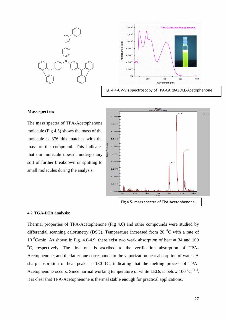
Mass spectra:
The mass spectra of TPA-Acetophenone
molecule (Fig 4.5) shows the mass of the
molecule is 376 this matches with the
mass of the compound. This indicates
that our molecule doesn’t undergo any
sort of further breakdown or splitting to
small molecules during the analysis.
4.2. TGA-DTA analysis:
Thermal properties of TPA-Acetophenone (Fig 4.6) and other compounds were studied by
differential scanning calorimetry (DSC). Temperature increased from 20 0C with a rate of
10 0C/min. As shown in Fig. 4.6-4.9, there exist two weak absorption of heat at 34 and 100
0C, respectively. The first one is ascribed to the verification absorption of TPA-
Acetophenone, and the latter one corresponds to the vaporization heat absorption of water. A
sharp absorption of heat peaks at 130 1C, indicating that the melting process of TPA-
Acetophenone occurs. Since normal working temperature of white LEDs is below 100 0C
[41],
it is clear that TPA-Acetophenone is thermal stable enough for practical applications.
O
N
Fig. 4.4-UV-Vis spectroscopy of TPA-CARBAZOLE-Acetophenone
Fig 4.5- mass spectra of TPA-Acetophenone
28
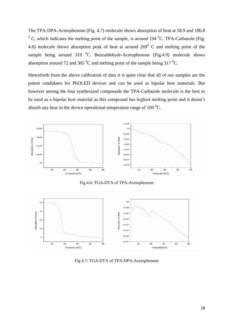
The TPA-DPA-Acetophenone (Fig. 4.7) molecule shows absorption of heat at 58.9 and 186.8
0 C, which indicates the melting point of the sample, is around 194
0C. TPA-Carbazole (Fig.
4.8) molecule shows absorption peak of heat at around 2690 C and melting point of the
sample being around 319 0C. Benzaldehyde-Acetophenone (Fig.4.9) molecule shows
absorption around 72 and 305 0C and melting point of the sample being 317
0C.
Henceforth from the above calibration of data it is quite clear that all of our samples are the
potent candidates for PhOLED devices and can be used as bipolar host materials. But
however among the four synthesized compounds the TPA-Carbazole molecule is the best to
be used as a bipolar host material as this compound has highest melting point and it doesn’t
absorb any hear in the device operational temperature range of 100 0C.
Fig 4.6: TGA-DTA of TPA-Acetophenone
Fig 4.7: TGA-DTA of TPA-DPA-Acetophenone

29
Fig 4.8: TGA-DTA of TPA-Carbazole-Acetophenone
Fig 4.9: TGA-DTA of Benzaldehyde-Acetophenone
4.3.Fluorescence studies:
The Photo Luminescence Spectroscopy of the TPA-Acetophenone and TPA-Carbazole-
Acetophenone compounds were measured at 344 and 413 nm emission range respectively.
The emission patterns are obtained as shown in the Fig.4.10 which indicates that TPA-
Acetophenone emits at 507 nm and TPA-Carbazole-Acetophenone emits at 544 nm
respectively. Also with increase in the conjugation at the hole transporting moiety side the
emission wavelength approach toward red shift due to probable decrease in HOMO-LUMO
energy gap. The intensity of emission of TPA-Carbazole-Acetophenone is also more than that
of TPA-Acetophenone. Therefore the latter one is a potent candidate for bipolar host
material.

30
Fig 4.10: PL spectra of TPA-Acetophenone and TPA-Carbazole-Acetophenone

31
Chapter 5
Conclusion and Outlook
5.1.Summary: In our synthesized compounds when the conjugation of electron transporting
group is increasing we are obtaining a emission colour which tends towards Red shift.
The basic reason is that as we go on increasing the conjugation the HOMO and LUMO
energy gap decreases and consequently a Red shift is obtained. We can play with bipolar
host structure and tune the structure to get an appropriate structure of our desire, which
yields a large variety of substrate scope which can be implemented as bipolar host
materials in PhOLEDs.
To achieve high efficiency PhOLEDs, the appropriate host materials are of equal
importance to the phosphorescent emitters. In this work we have synthesized novel
bipolar host materials that can have a potent application in PhOLEDs. The key qualities
of the host materials like relationship between the molecular structure of hosts and their
thermal, electrochemical and photophysical properties have been addressed. In general, to
design a host for a blue phosphor, a high enough triplet energy is main concern; to design
a host for green or red phosphor, relatively narrow energy gap and matched HOMO and
LUMO levels with adjacent layers are desirable. The good charge transporting ability and
high glass transition temperatures of host materials benefit the device performance.
5.2. Future work: Typical properties of host materials like triplet energy gap, charge
transporting ability, HOMO/LUMO level, and glass transition temperature should be
addressed. Up to date, green and red PhOLEDs with 100% internal quantum efficiency
have been achieved, but highly efficient and stable blue PhOLEDs remain to be further
developed. Moreover, the low efficiency and instability of blue PhOLEDs become a
bottleneck to the development of efficient and stable white PhOLEDs. In this regard, a
bipolar host capable of hosting a blue phosphor can play a vital role because a bipolar
host could not only broaden the exciton-formation zone, consequently reduce efficiency
roll-off, but also simplify the device structures by the employment of a single emitting
layer comprising of a bipolar host and two or more phosphors. Systematic engineering is
required to achieve highly efficient and stable PhOLEDs. It is only through the close
collaboration between both chemists and physicists that continuous promising advances
in this area can be attained. We hope the host materials will render highly efficient, stable,
and solution-processable phosphorescent OLEDs for commercial application.

32
References:
1) Burroughes, J. H.; Bradley, D. D. C.; Brown, A. R.; Marks, R. N.; Mackay, K.; Friend, R.
H.; Burns, P. L.; Holmes, A. B. Nature 1990, 347, 539.
2) a) Tokito, S.; Iijima, T.; Suzuri, Y.; Kita, H.; Tsuzuki, T.; Sato, F. Appl. Phys. Lett. 2003,
83, 569; b) Walzer, K.; Maenning, B.; Pfeiffer, M.; Leo, K. Chem. Rev. 2007, 107, 1233;
3) Wohlgenannt, M.; Tandon, K.; Mazumdar, S.; Ramasesha, S.; Vardeny, Z. V. Nature
2001, 409, 494.
4) Reineke, S.; Schwartz, G.; Walzer, K.; Falke, M.; Leo, K. Appl. Phys. Lett. 2009, 94,
163305
5) Holmes, R. J.; Forrest, S. R.; Tung, Y. –J.; Kwong, R. C.; Brown, J. J.; Garon, S.;
Thompson, M. E. Appl. Phys. Lett. 2003, 82, 2422-2424;
6) N. Zheludev, Nature Photonics, 2007, 1, 189.
7) M. A. Baldo, D. F. O'Brien, M. E. Thompson, S. R. Forrest, Phys. Rev. B, 1999,
60,14422.
8) C. Rothe, S. M. King, A. P. Monkman, Phys. Rev. Lett., 2006, 97, 076602.
9) M. A. Baldo, Von Slyke, D. F. O'Brien, Y. You, A. Shoustikov, S. Sibley, M. E.
Thompson, S. R. Forrest, Nature, 1998, 395,151.
10) C. Adachi, S. Tokito, T. Tsutsui, S. Saito, Jpn. J. Appl. Phys., 1988, 27, L713.
11) Von Slyke, Chen, S. Tokito, T. Tsutsui, S. Saito, Jpn. J. Appl. Phys., 1988, 27, L269.
12) J. H. Burrows, D. D. C. Bradley, A. R. Brown, R. N. Marks, K. Mackay, R. H. Friend, P.
L. Burns, A.B. Holmes, Nature, 1990, 347, 539.
13) Tang, C. W.; VanSlyke, S. A. Appl. Phys. Lett. 1987, 51, 913-915.
14) D’Andrade, B.; Forrest, S. R. Adv. Mater. 2004, 16, 1585-1595.
15) Misra, A.; Kumar, P.; Kamalasana, S. Semicond. Sci. Technol. 2006, 21, R35- R47.
16) Schwartz, G.; Reineke, S.; Rossenow, T. C.; Walzer, K.; Leo, K. Adv. Funct. Mater.
2009, 19, 1319
17) Baldo, M. A.; O’Brien, D. F.; You, Y.; Shoustikov, A.; Sibley, S.; Thompson, M. E.;
Forrest, S. R. Nature 1998, 395, 151-154.
18) Tokito, S.; Iijima, T.; Suzuri, Y.; Kita, H.; Tsuzuki, T.; Sato, F. Appl. Phys. Lett. 2003,
83, 569-571
19) Baldo et al., M. E. Appl. Phys. Lett. 2003, 82, 2422-2424
20) Sun, Y. R.; Giebink, N. C.; Kanno, H.; Ma, B.; Thompson, M. E.; Forrest, S. R. Nature,
2006, 440, 908-912.
33
21) Lane, P. A.; Palilis, L. C.; O'Brien, D. F.; Giebeler, C.; Cadby, A. J.; Lidzey, D. G.;
Campbell, A. J.; Blau, W.; Bradley, D. D. C. Phys. Rev. B. 2001, 63, 235206.
22) Holmes, R. J.; D’Andrade, B.; Forrest, S. R.; Ren, X.; Li, F.; Thompson, M. E. Appl.
Phys. Lett. 2003, 83, 3813.
23) Gong, X.; Ostrowski, J. C.; Moses, D.; Bazan, G. C.; Heeger, A. J. Adv. Funct. Mater.
2003, 13, 439-444
24) Yang, X. H.; Jaiser, F.; Neher, D. In Highly Efficient OLED with Phosphorescent
Materials; Yersin, H., Eds.; Wiley-VCH: Weinheim (Germany), 2008, pp 221-258
25) Ren, X. F.; Li, J.; Holmes, R. J.; Djurovich, P. I.; Forrest, S. R.; Thompson, M. E. Chem.
Mater. 2004, 16, 4743-4747
26) Tsai, M. -H.; Lin, H. -W.; Su, H. -C.; Ke, T. -H.; Wu, C. -C.; Fang, F. -C.; Liao, Y. -L.;
Wong, K. -T.; Wu, C. -I. Adv. Mater. 2006, 18, 1216
27) Walzer, K.; Maenning, B.; Pfeiffer, M.; Leo, K. Chem. Rev. 2007, 107, 1233- 1271.
28) Adachi, C.; Baldo, M.; Thompson, M. E.; Forrest, S. R. J. Appl. Phys. 2001, 90, 5048.
29) Reineke, S.; Walzer, K.; Leo, K. Phys. Rev. B 2007, 75, 125328.
30) Baldo, M. A.; Adachi, C.; Forrest, S. R. Phys. Rev. B. 2000, 62, 10967-10977.
31) Giebink, N. C.; Forrest, S. R. Phys. Rev. B 2008, 77, 235215.
32) Reineke, S.; Schwartz, G; Walzer, K.; Leo, K. Appl. Phys. Lett. 2007, 91, 123508.
33) Staroske, W.; Pfeiffer, M.; Leo, K.; Hoffmann, M. Phys. Rev. Lett. 2007, 98, 197402.
34) Chin, B. D.; Lee, C. Adv. Mater. 2007, 19, 2061-2066.
35) Meerheim, R.; Scholz, S.; Olthof, S.; Schwartz, G.; Reineke, S.; Walzer, K.; Leo, K. J.
Appl. Phys. 2008, 104, 014510.
36) W.-Y. Wong and C.-L. Ho, Coord. Chem. Rev., 2009, 253, 1709.
37) C. Ulbricht, B. Beyer, C. Friebe, A. Winter and U. S. Schubert, Adv. Mater., 2009, 21,
4418.
38) H. Chen, H. Li, H. Zhang, H. Zhang, J. Funct. Mater. 35 (2004) 750.
39) N. Armroli, L. De Cola, V. Balzami, J.P. Sauvage, C.D. Dietich Buchecker, J.M. Kern, J.
Chem. Soc. Faraday Trans. 88 (1992) 553.
40) Liming Zhang et al. Journal of Luminescence 128 (2008) 67–73
41) S. Feng, X. Xie, C. Lv, X. Zhang, Y. He, G. Shen, Chin. J. Semicond. 20 (1999)358.


