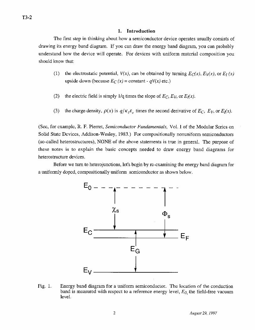
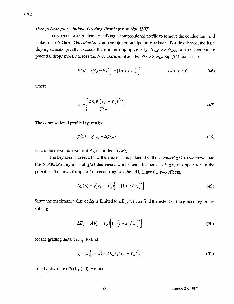
×
Log in
Upload File
Most Popular
Study
Business
Design
Technology
Travel
Explore all categories
Download -
T3: Heterostructure Fundamentals for HBTs
Download
Transcript
Page 1
Page 2
Page 3
Page 4
Page 5
Page 6
Page 7
Page 8
Page 9
Page 10
Page 11
Page 12
Page 13
Page 14
Page 15
Page 16
Page 17
Page 18
Page 19
Page 20
Page 21
Page 22
Page 23
Page 24
Page 25
Page 26
Page 27
Page 28
Page 29
Page 30
Page 31
Page 32
Page 33
Page 34
Page 35
Page 36
Page 37
Page 38
Page 39
Page 40
Page 41
Page 42
Page 43
LOAD MORE
Top Related
Process Technologies For Sub-100-nm InP HBTs & InGaAs MOSFETs
0) · 2016. 7. 8. · x\hsp[`th`]hy`klwlukpunvu svjh[pvu ;opz^psshhlj[Äuhs lhkpunz ... pj /\tpjhjpk)sluk-sv^ly luohujly t3 t3 t3 t3 t3 t3 t3 t3 t3 t3 t3 t3 t3 t3 t3 t3 t3 t3 t3 t3
InP-based HBTs: Devices and GHz mixed-signal ICs
Facile one-pot synthesis of heterostructure SnO2/ZnO
Nov. 2011 - HBTS News
Characteristics of Submicron HBTs in the 140-220 GHz Band
Nobel Lecture: The double heterostructure concept and its
SiGe HBTs and BiCMOS Technology for Present and Future


![0) · 2016. 7. 8. · x\hsp[`th`]hy`klwlukpunvu svjh[pvu ;opz^psshhlj[Äuhs lhkpunz ... pj /\tpjhjpk)sluk-sv^ly luohujly t3 t3 t3 t3 t3 t3 t3 t3 t3 t3 t3 t3 t3 t3 t3 t3 t3 t3 t3 t3](https://cdn.vdocument.in/doc/165x107/60d98d4a31005a4c8d3c5fa4/0-2016-7-8-xhspthhyklwlukpunvu-svjhpvu-opzpsshhljuhs-lhkpunz-.jpg)


