drm006, general-purpose 3-phase ac industrial motor ... · general-purpose 3-phase ac industrial...
TRANSCRIPT
WWW.MOTOROLA.COM/SEMICONDUCTORS
MC3PHACMotor Controller
DRM006/D4/2002
General-Purpose3-Phase AC Industrial
Designer Reference Manual
Motor Controller
Fre
esc
ale
Se
mic
on
du
cto
r, I
Freescale Semiconductor, Inc.
For More Information On This Product, Go to: www.freescale.com
nc
...

Fre
esc
ale
Se
mic
on
du
cto
r, I
Freescale Semiconductor, Inc.
For More Information On This Product, Go to: www.freescale.com
nc
...

F
ree
sca
le S
em
ico
nd
uc
tor,
IFreescale Semiconductor, Inc.
nc
...
General-Purpose 3-PhaseAC Industrial Motor ControllerReference DesignDesigner Reference Manual
Motorola reserves the right to make changes without further notice to any productsherein. Motorola makes no warranty, representation or guarantee regarding thesuitability of its products for any particular purpose, nor does Motorola assume anyliability arising out of the application or use of any product or circuit, and specificallydisclaims any and all liability, including without limitation consequential or incidentaldamages. "Typical" parameters which may be provided in Motorola data sheets and/orspecifications can and do vary in different applications and actual performance mayvary over time. All operating parameters, including "Typicals" must be validated foreach customer application by customer's technical experts. Motorola does not conveyany license under its patent rights nor the rights of others. Motorola products are notdesigned, intended, or authorized for use as components in systems intended forsurgical implant into the body, or other applications intended to support or sustain life,or for any other application in which the failure of the Motorola product could create asituation where personal injury or death may occur. Should Buyer purchase or useMotorola products for any such unintended or unauthorized application, Buyer shallindemnify and hold Motorola and its officers, employees, subsidiaries, affiliates, anddistributors harmless against all claims, costs, damages, and expenses, andreasonable attorney fees arising out of, directly or indirectly, any claim of personalinjury or death associated with such unintended or unauthorized use, even if such claimalleges that Motorola was negligent regarding the design or manufacture of the part.Motorola, Inc. is an Equal Opportunity/Affirmative Action Employer.
Motorola and are registered trademarks of Motorola, Inc.DigitalDNA is a trademark of Motorola, Inc. © Motorola, Inc., 2002
3-Phase AC Industrial Motor Controller Designer Reference Manual
MOTOROLA 3 For More Information On This Product,
Go to: www.freescale.com

Designer Reference Manual
F
ree
sca
le S
em
ico
nd
uc
tor,
I
Freescale Semiconductor, Inc.n
c..
.
To provide the most up-to-date information, the revision of ourdocuments on the World Wide Web will be the most current. Your printedcopy may be an earlier revision. To verify you have the latest informationavailable, refer to the documentation library available at:
http://www.motorola.com/semiconductor
Designer Reference Manual 3-Phase AC Industrial Motor Controller
4 MOTOROLA For More Information On This Product,
Go to: www.freescale.com
F
ree
sca
le S
em
ico
nd
uc
tor,
IFreescale Semiconductor, Inc.
nc
...
Designer Reference Manual — 3-Phase AC Industrial Motor Controller
List of Sections
Section 1. Introduction and Setup. . . . . . . . . . . . . . . . . .13
Section 2. Operational Description . . . . . . . . . . . . . . . . .33
Section 3. Pin Descriptions . . . . . . . . . . . . . . . . . . . . . . .41
Section 4. Schematics and Parts List . . . . . . . . . . . . . . .47
Section 5. Design Considerations . . . . . . . . . . . . . . . . . .55
Appendix A. MC3PHAC Data Sheet . . . . . . . . . . . . . . . .63
3-Phase AC Industrial Motor Controller Designer Reference Manual
MOTOROLA List of Sections 5 For More Information On This Product,
Go to: www.freescale.com

List of Sections
F
ree
sca
le S
em
ico
nd
uc
tor,
I
Freescale Semiconductor, Inc.n
c..
.
Designer Reference Manual 3-Phase AC Industrial Motor Controller
6 List of Sections MOTOROLA For More Information On This Product,
Go to: www.freescale.com
F
ree
sca
le S
em
ico
nd
uc
tor,
IFreescale Semiconductor, Inc.
nc
...
Designer Reference Manual — 3-Phase AC Industrial Motor Controller
Table of Contents
Section 1. Introduction and Setup
1.1 Contents . . . . . . . . . . . . . . . . . . . . . . . . . . . . . . . . . . . . . . . . . .13
1.2 Introduction . . . . . . . . . . . . . . . . . . . . . . . . . . . . . . . . . . . . . . . .13
1.3 Brief Overview to 3-Phase Induction Motors . . . . . . . . . . . . . .14
1.4 About this Manual . . . . . . . . . . . . . . . . . . . . . . . . . . . . . . . . . . .18
1.5 Features . . . . . . . . . . . . . . . . . . . . . . . . . . . . . . . . . . . . . . . . . .19
1.6 Warnings. . . . . . . . . . . . . . . . . . . . . . . . . . . . . . . . . . . . . . . . . .20
1.7 Setup Guide . . . . . . . . . . . . . . . . . . . . . . . . . . . . . . . . . . . . . . .21
Section 2. Operational Description
2.1 Contents . . . . . . . . . . . . . . . . . . . . . . . . . . . . . . . . . . . . . . . . . .33
2.2 Introduction . . . . . . . . . . . . . . . . . . . . . . . . . . . . . . . . . . . . . . . .33
2.3 Electrical Characteristics . . . . . . . . . . . . . . . . . . . . . . . . . . . . .35
2.4 User Interfaces . . . . . . . . . . . . . . . . . . . . . . . . . . . . . . . . . . . . .352.4.1 Potentiometers . . . . . . . . . . . . . . . . . . . . . . . . . . . . . . . . . . .352.4.2 Switches . . . . . . . . . . . . . . . . . . . . . . . . . . . . . . . . . . . . . . . .372.4.3 Jumpers . . . . . . . . . . . . . . . . . . . . . . . . . . . . . . . . . . . . . . . .382.4.4 Indicator Lights . . . . . . . . . . . . . . . . . . . . . . . . . . . . . . . . . . .392.4.5 Test Points . . . . . . . . . . . . . . . . . . . . . . . . . . . . . . . . . . . . . .392.4.6 Optoisolated RS232 Interface . . . . . . . . . . . . . . . . . . . . . . .40
Section 3. Pin Descriptions
3.1 Contents . . . . . . . . . . . . . . . . . . . . . . . . . . . . . . . . . . . . . . . . . .41
3.2 Introduction . . . . . . . . . . . . . . . . . . . . . . . . . . . . . . . . . . . . . . . .41
3.3 Control Board Signal Descriptions . . . . . . . . . . . . . . . . . . . . . .41
3-Phase AC Industrial Motor Controller Designer Reference Manual
MOTOROLA Table of Contents 7 For More Information On This Product,
Go to: www.freescale.com

Table of Contents
F
ree
sca
le S
em
ico
nd
uc
tor,
I
Freescale Semiconductor, Inc.n
c..
.
3.3.1 40-Pin Connector J1. . . . . . . . . . . . . . . . . . . . . . . . . . . . . . .413.3.2 Optoisolated RS232 DB-9 Connector J2 . . . . . . . . . . . . . . .453.3.3 Power Connector J3. . . . . . . . . . . . . . . . . . . . . . . . . . . . . . .45
Section 4. Schematics and Parts List
4.1 Contents . . . . . . . . . . . . . . . . . . . . . . . . . . . . . . . . . . . . . . . . . .47
4.2 Schematics . . . . . . . . . . . . . . . . . . . . . . . . . . . . . . . . . . . . . . . .47
4.3 Parts Lists . . . . . . . . . . . . . . . . . . . . . . . . . . . . . . . . . . . . . . . . .51
Section 5. Design Considerations
5.1 Contents . . . . . . . . . . . . . . . . . . . . . . . . . . . . . . . . . . . . . . . . . .55
5.2 Overview. . . . . . . . . . . . . . . . . . . . . . . . . . . . . . . . . . . . . . . . . .55
5.3 Dead Time . . . . . . . . . . . . . . . . . . . . . . . . . . . . . . . . . . . . . . . .55
5.4 Power-Up/Power-Down . . . . . . . . . . . . . . . . . . . . . . . . . . . . . .56
5.5 Grounding . . . . . . . . . . . . . . . . . . . . . . . . . . . . . . . . . . . . . . . . .56
5.6 Fault Circuits. . . . . . . . . . . . . . . . . . . . . . . . . . . . . . . . . . . . . . .56
5.7 On-Board Power Supply . . . . . . . . . . . . . . . . . . . . . . . . . . . . . .59
5.8 Optoisolated RS232 Interface. . . . . . . . . . . . . . . . . . . . . . . . . .60
Appendix A. MC3PHAC Data Sheet
Designer Reference Manual 3-Phase AC Industrial Motor Controller
8 Table of Contents MOTOROLA For More Information On This Product,
Go to: www.freescale.com
F
ree
sca
le S
em
ico
nd
uc
tor,
IFreescale Semiconductor, Inc.
nc
...
Designer Reference Manual — 3-Phase AC Industrial Motor Controller
List of Figures
Figure Title Page
1-1 Board Photograph. . . . . . . . . . . . . . . . . . . . . . . . . . . . . . . . . . .141-2 Schematic View of a 3-Phase AC induction Motor . . . . . . . . . .161-3 3-Phase AC Motor Drive. . . . . . . . . . . . . . . . . . . . . . . . . . . . . .171-4 System’s Configurations . . . . . . . . . . . . . . . . . . . . . . . . . . . . . .191-5 System Setup . . . . . . . . . . . . . . . . . . . . . . . . . . . . . . . . . . . . . .211-6 Dead Time vs. Resistance . . . . . . . . . . . . . . . . . . . . . . . . . . . .281-7 Retry Time vs. Resistance . . . . . . . . . . . . . . . . . . . . . . . . . . . .291-8 Voltage Boost vs. Resistance . . . . . . . . . . . . . . . . . . . . . . . . . .31
2-1 Reference PC Board Block Diagram . . . . . . . . . . . . . . . . . . . .34
3-1 40-Pin Ribbon Connector J1. . . . . . . . . . . . . . . . . . . . . . . . . . .42
4-1 MC3PHAC Reference Board Circuitry (Sheet 1 of 3) . . . . . . . .484-2 MC3PHAC Reference Board Circuitry (Sheet 2 of 3) . . . . . . . .494-3 MC3PHAC Reference Board Circuitry (Sheet 3 of 3) . . . . . . . .50
5-1 Overvoltage Fault Circuit . . . . . . . . . . . . . . . . . . . . . . . . . . . . .575-2 Overtemperature Fault Circuit . . . . . . . . . . . . . . . . . . . . . . . . .585-3 On-Board Power Supply . . . . . . . . . . . . . . . . . . . . . . . . . . . . . .595-4 RS232 Interface . . . . . . . . . . . . . . . . . . . . . . . . . . . . . . . . . . . .60
3-Phase AC Industrial Motor Controller Designer Reference Manual
MOTOROLA List of Figures 9 For More Information On This Product,
Go to: www.freescale.com

List of Figures
F
ree
sca
le S
em
ico
nd
uc
tor,
I
Freescale Semiconductor, Inc.n
c..
.
Designer Reference Manual 3-Phase AC Industrial Motor Controller
10 List of Figures MOTOROLA For More Information On This Product,
Go to: www.freescale.com
F
ree
sca
le S
em
ico
nd
uc
tor,
IFreescale Semiconductor, Inc.
nc
...
Designer Reference Manual — 3-Phase AC Industrial Motor Controller
List of Tables
Table Title Page
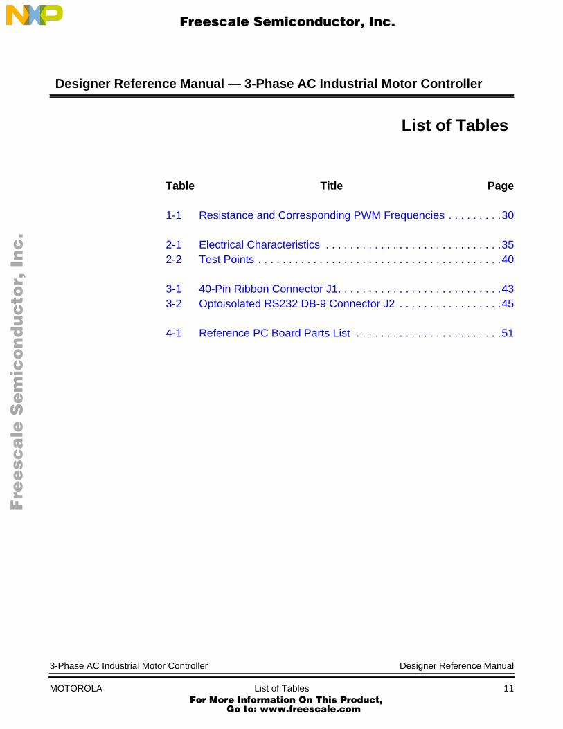
1-1 Resistance and Corresponding PWM Frequencies . . . . . . . . .30
2-1 Electrical Characteristics . . . . . . . . . . . . . . . . . . . . . . . . . . . . .352-2 Test Points . . . . . . . . . . . . . . . . . . . . . . . . . . . . . . . . . . . . . . . .40
3-1 40-Pin Ribbon Connector J1. . . . . . . . . . . . . . . . . . . . . . . . . . .433-2 Optoisolated RS232 DB-9 Connector J2 . . . . . . . . . . . . . . . . .45
4-1 Reference PC Board Parts List . . . . . . . . . . . . . . . . . . . . . . . .51
3-Phase AC Industrial Motor Controller Designer Reference Manual
MOTOROLA List of Tables 11 For More Information On This Product,
Go to: www.freescale.com

List of Tables
F
ree
sca
le S
em
ico
nd
uc
tor,
I
Freescale Semiconductor, Inc.n
c..
.
Designer Reference Manual 3-Phase AC Industrial Motor Controller
12 List of Tables MOTOROLA For More Information On This Product,
Go to: www.freescale.com
F
ree
sca
le S
em
ico
nd
uc
tor,
IFreescale Semiconductor, Inc.
nc
...
Designer Reference Manual — 3-Phase AC Industrial Motor Controller
Section 1. Introduction and Setup
1.1 Contents
1.2 Introduction . . . . . . . . . . . . . . . . . . . . . . . . . . . . . . . . . . . . . . . .13
1.3 Brief Overview to 3-Phase Induction Motors . . . . . . . . . . . . . .14
1.4 About this Manual . . . . . . . . . . . . . . . . . . . . . . . . . . . . . . . . . . .18
1.5 Features . . . . . . . . . . . . . . . . . . . . . . . . . . . . . . . . . . . . . . . . . .19
1.6 Warnings. . . . . . . . . . . . . . . . . . . . . . . . . . . . . . . . . . . . . . . . . .20
1.7 Setup Guide . . . . . . . . . . . . . . . . . . . . . . . . . . . . . . . . . . . . . . .21
1.2 Introduction
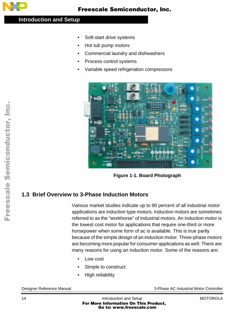
Motorola’s MC3PHAC motor control reference PC board is designed foruse with optoisolation and power modules that are an integral part of theembedded motion control series of development tools. It may be usedwith custom power stages as well, and it is intended as a vehicle toevaluate the MC3PHAC motor control device. The MC3PHAC isdesigned to provide all of the necessary pulse-width modulated outputsand monitor the system parameters necessary to control a 3-phaseinduction motor. The reference PC board interfaces easily with powerstages and optoisolator boards. Details of the interface are given inSection 3. Pin Descriptions. A photograph of the board is shown inFigure 1-1.
Some applications for this system include:
• Low horsepower, variable-speed HVAC compressors, blowers,and air handler motors
• Garage door openers
• Variable-speed pumps
• Submersible pumps
3-Phase AC Industrial Motor Controller Designer Reference Manual
MOTOROLA Introduction and Setup 13 For More Information On This Product,
Go to: www.freescale.com
Introduction and Setup
F
ree
sca
le S
em
ico
nd
uc
tor,
I
Freescale Semiconductor, Inc.n
c..
.
• Soft-start drive systems
• Hot tub pump motors
• Commercial laundry and dishwashers
• Process control systems
• Variable speed refrigeration compressors
Figure 1-1. Board Photograph
1.3 Brief Overview to 3-Phase Induction Motors
Various market studies indicate up to 90 percent of all industrial motorapplications are induction type motors. Induction motors are sometimesreferred to as the “workhorse” of industrial motors. An induction motor isthe lowest cost motor for applications that require one-third or morehorsepower when some form of ac is available. This is true partlybecause of the simple design of an induction motor. Three-phase motorsare becoming more popular for consumer applications as well. There aremany reasons for using an induction motor. Some of the reasons are:
• Low cost
• Simple to construct
• High reliability
Designer Reference Manual 3-Phase AC Industrial Motor Controller
14 Introduction and Setup MOTOROLA For More Information On This Product,
Go to: www.freescale.com

Introduction and SetupBrief Overview to 3-Phase Induction Motors
F
ree
sca
le S
em
ico
nd
uc
tor,
I
Freescale Semiconductor, Inc.n
c..
.
• High efficiency
• No brushes to wear out
• Operate well in extreme temperature conditions
• Minimum maintenance
In the case of the system described in this document, the ac power forthe 3-phase induction motor is generated by an inverter, driven from apulse-width modulator (PWM) within the MC3PHAC controller.
These advantages do not come without a price. An induction motor’sspeed is difficult to control due to its complex mathematical model andits non-linear behavior when its core is saturated. Semiconductor-basedcontrol systems have enabled the use of induction motors for manyapplications requiring speed control.
Induction motors are available in a wide range of sizes, from less thanone watt to thousands of kilowatts. Common input voltage ranges are230 and 460 volts for 60 Hz and input voltages of 380 volts whenoperating at 50 Hz.
The motors are available in a variety of mounting styles. Mounting stylesinclude C-face, foot mount, large flange, vertical, and custom mounts.Depending on the environment where the motor will reside, open,explosion proof, totally enclosed, fan-cooled, water-cooled,blower-cooled, and other enclosures are available.
An ac induction motor consists of two windings. The windings are therotor and stator assemblies. An induction motor can be thought of as atransformer with a fixed primary (stator) and a rotating secondary (rotor).The motor’s name “induction” comes from the fact that alternatingcurrents are induced from the stator into the rotor by the rotatingmagnetic flux produced in the stator. The motor’s torque is developedfrom the interaction of the currents flowing in the rotor and the stator’srotating magnetic field. The stator, or primary, windings connect to the3-phase voltage source to produce a rotating magnetic field. The statorstructure is constructed with steel laminations shaped to form poles thatare wound with copper wire coils. The rotor is an assembly oflaminations over a steel shaft core. Radial slots around the laminationsperiphery house copper or aluminum conductors at one end and are
3-Phase AC Industrial Motor Controller Designer Reference Manual
MOTOROLA Introduction and Setup 15 For More Information On This Product,
Go to: www.freescale.com
Introduction and Setup
F
ree
sca
le S
em
ico
nd
uc
tor,
I
Freescale Semiconductor, Inc.n
c..
.
positioned in parallel to the shaft. The primary windings are connectedto a 3-phase power source which produce a rotating magnetic field. Inthe case of a 3-phase induction motor, the primary or stator windings arespaced physically 120 degrees apart. If you view the rotor from one end,it appears to look like a squirrel cage. Sometimes an induction motor isreferred to as a squirrel cage induction motor.
Figure 1-2 shows a schematic view of the construction of a 3-phase acinduction motor.
Figure 1-2. Schematic View of a 3-Phase AC induction Motor
The magnetic field in the stator rotates at a synchronous speed aroundthe parameter of the stator with the applied power’s frequency. Thespeed of an ac induction motor is controlled by the following factors:
• The number of poles (winding sets) built into the motor
• The frequency of the ac line voltage
• The amount of torque loading, which causes slippage
In actual practice, the rotor speed of the motor will always lag the rotatingmagnetic field of the stator. Typical slip values range from 2 percent to5 percent of the theoretical rotational speed. Slip will always increasewith the applied loading of the motor.
STATOR
ROTOR
ROTATING FIELD (ωs)
TORQUE
INDUCED CURRENTωr
Designer Reference Manual 3-Phase AC Industrial Motor Controller
16 Introduction and Setup MOTOROLA For More Information On This Product,
Go to: www.freescale.com
Introduction and SetupBrief Overview to 3-Phase Induction Motors
F
ree
sca
le S
em
ico
nd
uc
tor,
I
Freescale Semiconductor, Inc.n
c..
.
To put the rotation speed in equation form, the theoretical speed of themotor shaft is Vs = 120 (input frequency/number of poles). For a 60-Hzfixed frequency and a motor with four poles, the theoretical speed wouldbe 1800 rpm. However, taking slip into consideration, using 4 percentslip, the actual speed of the motor would be 1728 rpm.
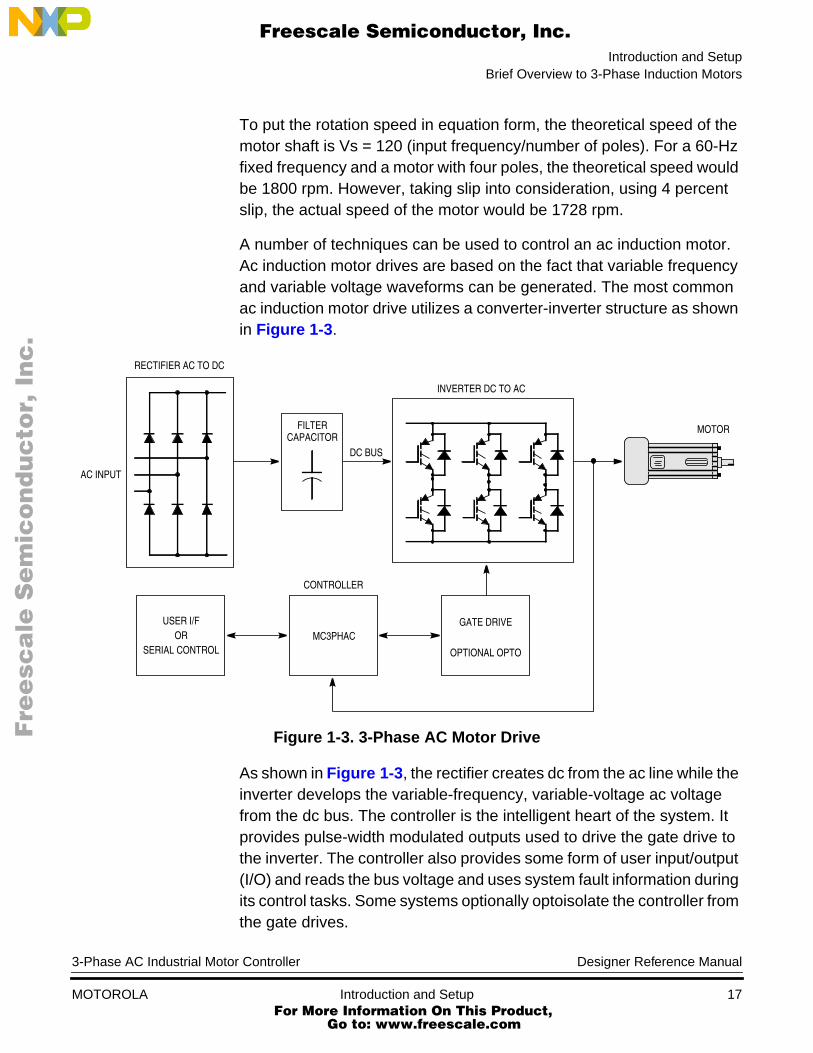
A number of techniques can be used to control an ac induction motor.Ac induction motor drives are based on the fact that variable frequencyand variable voltage waveforms can be generated. The most commonac induction motor drive utilizes a converter-inverter structure as shownin Figure 1-3.
Figure 1-3. 3-Phase AC Motor Drive
As shown in Figure 1-3, the rectifier creates dc from the ac line while theinverter develops the variable-frequency, variable-voltage ac voltagefrom the dc bus. The controller is the intelligent heart of the system. Itprovides pulse-width modulated outputs used to drive the gate drive tothe inverter. The controller also provides some form of user input/output(I/O) and reads the bus voltage and uses system fault information duringits control tasks. Some systems optionally optoisolate the controller fromthe gate drives.
MOTOR
RECTIFIER AC TO DC
AC INPUT
FILTERCAPACITOR
DC BUS
INVERTER DC TO AC
GATE DRIVE
OPTIONAL OPTO
MC3PHAC
CONTROLLER
USER I/FOR
SERIAL CONTROL
3-Phase AC Industrial Motor Controller Designer Reference Manual
MOTOROLA Introduction and Setup 17 For More Information On This Product,
Go to: www.freescale.com
Introduction and Setup
F
ree
sca
le S
em
ico
nd
uc
tor,
I
Freescale Semiconductor, Inc.n
c..
.
Many excellent text and reference books describe motors and theircontrol techniques. A list containing several of them is presented here:
• Motor Control Electronics Handbook, by Richard Valentine,McGraw-Hill, 1998, ISBN 0-07-066810-8
• DC Motors, Speed Controls, Servo Systems, by Electro-CraftCorp., 1980, ISBN 0-9601914-0-2
• Electric Machinery, by A. E. Fitzgerald, Charles Kingsley Jr., andStephen D. Umans, McGraw-Hill, 1990, ISBN 0-07-021134-5
• Vector Control of AC Machines, by Peter Vas, Oxford UniversityPress, 1994, ISBN 0-19-859370-8
• Power Electronics, by Ned Mohan, Tore Undeland, and WilliamRobbins, John Wiley & Sons, 1995, ISBN 0-471-58408-8
• Power Electronics and Variable Frequency Drives, edited byBimal Bose, IEEE Press, 1997, ISBN 0-7803-1084-5
• Electric Drives, an Integrative Approach, by Ned Mohan,University of Minnesota Printing Services, 2000, ISBN0-9663530-1-3
1.4 About this Manual
Key items can be found in the following locations in this manual:
• Setup instructions are found in 1.7 Setup Guide.
• Schematics are found in Section 4. Schematics and Parts List.
• Pin assignments are shown in Figure 3-1. 40-Pin RibbonConnector J1, and a pin-by-pin description is contained in 3.3Control Board Signal Descriptions.
• For those interested in the reference design aspects of the board’scircuitry, a description is provided in Section 5. DesignConsiderations.
Designer Reference Manual 3-Phase AC Industrial Motor Controller
18 Introduction and Setup MOTOROLA For More Information On This Product,
Go to: www.freescale.com
Introduction and SetupFeatures
F
ree
sca
le S
em
ico
nd
uc
tor,
I
Freescale Semiconductor, Inc.n
c..
.
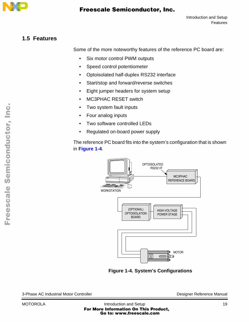
1.5 Features
Some of the more noteworthy features of the reference PC board are:
• Six motor control PWM outputs
• Speed control potentiometer
• Optoisolated half-duplex RS232 interface
• Start/stop and forward/reverse switches
• Eight jumper headers for system setup
• MC3PHAC RESET switch
• Two system fault inputs
• Four analog inputs
• Two software controlled LEDs
• Regulated on-board power supply
The reference PC board fits into the system’s configuration that is shownin Figure 1-4.
Figure 1-4. System’s Configurations
MC3PHAC
MOTOR
WORKSTATION
HIGH-VOLTAGEPOWER STAGE
(OPTIONAL)
BOARDOPTOISOLATION
OPTOISOLATEDRS232 I/F
REFERENCE BOARD
3-Phase AC Industrial Motor Controller Designer Reference Manual
MOTOROLA Introduction and Setup 19 For More Information On This Product,
Go to: www.freescale.com

Introduction and Setup
F
ree
sca
le S
em
ico
nd
uc
tor,
I
Freescale Semiconductor, Inc.n
c..
.
1.6 Warnings
This MC3PHAC reference PC board operates in an environment thatincludes dangerous voltages and rotating machinery.
To facilitate safe operation, input power for the high-voltage powerstages should come from a current limited dc laboratory power supply. Ifac power is applied directly to the power stage, an isolation transformershould be used.
When operating high-voltage power stages directly from an ac line,power stage grounds and oscilloscope grounds are at differentpotentials, unless the oscilloscope is floating. Note that probe groundsand, therefore, the case of a floated oscilloscope, are subjected todangerous voltages.
• Before moving scope probes, making connections, etc., you mustpower down the high-voltage supply.
• When high voltage is applied to the high-voltage power stage,using only one hand for operating the test setup minimizes thepossibility of electrical shock.
• Operation in lab setups that have grounded tables and/or chairsshould be avoided.
• Wearing safety glasses, avoiding ties and jewelry, using shields,and operation by personnel trained in high-voltage lab techniquesare also advisable.
Designer Reference Manual 3-Phase AC Industrial Motor Controller
20 Introduction and Setup MOTOROLA For More Information On This Product,
Go to: www.freescale.com
Introduction and SetupSetup Guide
F
ree
sca
le S
em
ico
nd
uc
tor,
I
Freescale Semiconductor, Inc.n
c..
.
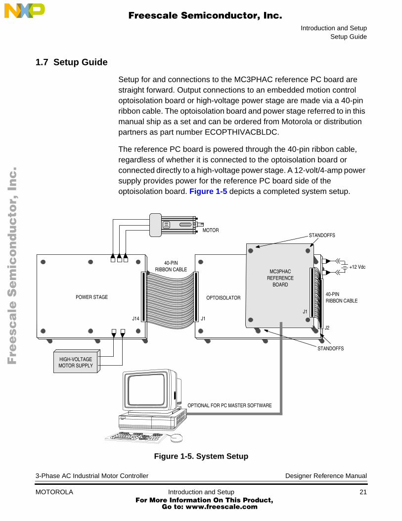
1.7 Setup Guide
Setup for and connections to the MC3PHAC reference PC board arestraight forward. Output connections to an embedded motion controloptoisolation board or high-voltage power stage are made via a 40-pinribbon cable. The optoisolation board and power stage referred to in thismanual ship as a set and can be ordered from Motorola or distributionpartners as part number ECOPTHIVACBLDC.
The reference PC board is powered through the 40-pin ribbon cable,regardless of whether it is connected to the optoisolation board orconnected directly to a high-voltage power stage. A 12-volt/4-amp powersupply provides power for the reference PC board side of theoptoisolation board. Figure 1-5 depicts a completed system setup.
Figure 1-5. System Setup
MOTOR
MC3PHAC
OPTOISOLATOR
40-PINRIBBON CABLE
POWER STAGE 40-PINRIBBON CABLE
STANDOFFS
STANDOFFS
+12 Vdc
HIGH-VOLTAGEMOTOR SUPPLY
J2
OPTIONAL FOR PC MASTER SOFTWARE
REFERENCEBOARD
J1J1J14
3-Phase AC Industrial Motor Controller Designer Reference Manual
MOTOROLA Introduction and Setup 21 For More Information On This Product,
Go to: www.freescale.com
Introduction and Setup
F
ree
sca
le S
em
ico
nd
uc
tor,
I
Freescale Semiconductor, Inc.n
c..
.
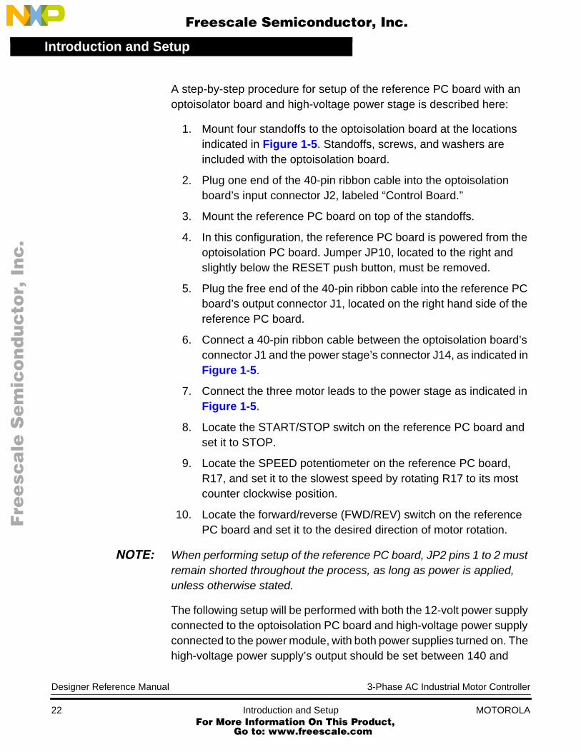
A step-by-step procedure for setup of the reference PC board with anoptoisolator board and high-voltage power stage is described here:
1. Mount four standoffs to the optoisolation board at the locationsindicated in Figure 1-5. Standoffs, screws, and washers areincluded with the optoisolation board.
2. Plug one end of the 40-pin ribbon cable into the optoisolationboard’s input connector J2, labeled “Control Board.”
3. Mount the reference PC board on top of the standoffs.
4. In this configuration, the reference PC board is powered from theoptoisolation PC board. Jumper JP10, located to the right andslightly below the RESET push button, must be removed.
5. Plug the free end of the 40-pin ribbon cable into the reference PCboard’s output connector J1, located on the right hand side of thereference PC board.
6. Connect a 40-pin ribbon cable between the optoisolation board’sconnector J1 and the power stage’s connector J14, as indicated inFigure 1-5.
7. Connect the three motor leads to the power stage as indicated inFigure 1-5.
8. Locate the START/STOP switch on the reference PC board andset it to STOP.
9. Locate the SPEED potentiometer on the reference PC board,R17, and set it to the slowest speed by rotating R17 to its mostcounter clockwise position.
10. Locate the forward/reverse (FWD/REV) switch on the referencePC board and set it to the desired direction of motor rotation.
NOTE: When performing setup of the reference PC board, JP2 pins 1 to 2 mustremain shorted throughout the process, as long as power is applied,unless otherwise stated.
The following setup will be performed with both the 12-volt power supplyconnected to the optoisolation PC board and high-voltage power supplyconnected to the power module, with both power supplies turned on. Thehigh-voltage power supply’s output should be set between 140 and
Designer Reference Manual 3-Phase AC Industrial Motor Controller
22 Introduction and Setup MOTOROLA For More Information On This Product,
Go to: www.freescale.com
Introduction and SetupSetup Guide
F
ree
sca
le S
em
ico
nd
uc
tor,
I
Freescale Semiconductor, Inc.n
c..
.
230 Vdc, based on the motor requirements. Prior to connecting thehigh-voltage power supply to the power module, adjust its output voltageto that required by your specific motor.
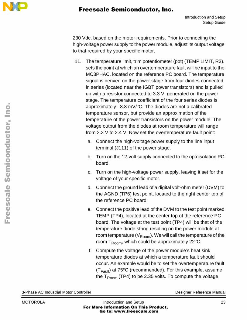
11. The temperature limit, trim potentiometer (pot) (TEMP LIMIT, R3).sets the point at which an overtemperature fault will be input to theMC3PHAC, located on the reference PC board. The temperaturesignal is derived on the power stage from four diodes connectedin series (located near the IGBT power transistors) and is pulledup with a resistor connected to 3.3 V, generated on the powerstage. The temperature coefficient of the four series diodes isapproximately –8.8 mV/°C. The diodes are not a calibratedtemperature sensor, but provide an approximation of thetemperature of the power transistors on the power module. Thevoltage output from the diodes at room temperature will rangefrom 2.3 V to 2.4 V. Now set the overtemperature fault point:
a. Connect the high-voltage power supply to the line inputterminal (J111) of the power stage.
b. Turn on the 12-volt supply connected to the optoisolation PCboard.
c. Turn on the high-voltage power supply, leaving it set for thevoltage of your specific motor.
d. Connect the ground lead of a digital volt-ohm meter (DVM) tothe AGND (TP6) test point, located to the right center top ofthe reference PC board.
e. Connect the positive lead of the DVM to the test point markedTEMP (TP4), located at the center top of the reference PCboard. The voltage at the test point (TP4) will be that of thetemperature diode string residing on the power module atroom temperature (VRoom). We will call the temperature of theroom TRoom, which could be approximately 22°C.
f. Compute the voltage of the power module’s heat sinktemperature diodes at which a temperature fault shouldoccur. An example would be to set the overtemperature fault(TFault) at 75°C (recommended). For this example, assumethe TRoom (TP4) to be 2.35 volts. To compute the voltage
3-Phase AC Industrial Motor Controller Designer Reference Manual
MOTOROLA Introduction and Setup 23 For More Information On This Product,
Go to: www.freescale.com

Introduction and Setup
F
ree
sca
le S
em
ico
nd
uc
tor,
I
Freescale Semiconductor, Inc.n
c..
.
from the diode string at 75°C (TFault), the following equationapplies: VTP4 = VRoom + ((TFault – TRoom) * – 0.0088).That is, the voltage at TP5 will be:1.88 V = 2.35 + ((75–22) * – 0.0088).
g. Connect the DVM to the TEMP LMT (temperature limit) testpoint TP5. Adjust the TEMP LIMIT (R3) trim pot such that thevoltage reads 1.88 volts on the DVM. The overtemperaturefault is now set for ~75°C, based on the values calculatedfrom the previous step.
12. The MC3PHAC requires the value of the high-voltage bus whenoperating. The bus voltage signal is derived on the power stagefrom a voltage divider connected to the high-voltage bus.
The voltage bus signal serves two purposes on the reference PCboard. The divided, high-voltage bus is amplified and used forsystem control and also serves as an input to the overvoltagefault-generating circuitry. Now set the bus voltage amplifier,followed by the overvoltage fault point, by:
a. Connect the ground lead of a DVM to the AGND (TP6) testpoint, located to the right center top of the reference PCboard.
b. Connect the positive lead of the DVM to the test point markedVBus (TP2), located at the left top of the reference PC board.
c. Adjust the VBus GAIN (R2) trim pot such that the voltagereads 3.5 volts on the DVM.
d. To adjust the point at which the MC3PHAC will receive anovervoltage fault, connect the positive lead of the DVM to thetest point marked VBus LIMIT (R1).
e. Adjust the VBus LIMIT (R1) trim pot such that the voltagereads 4.5 volts on the DVM.
13. If you are NOT using PC master software, skip to step 15.
14. If PC master software is used for real-time control of motoroperation, it is necessary to set up RS232 serial communicationwith a PC. To do this, connect a 9-conductor straight throughcable from the reference board’s DB-9 connector, J2, to the serial
Designer Reference Manual 3-Phase AC Industrial Motor Controller
24 Introduction and Setup MOTOROLA For More Information On This Product,
Go to: www.freescale.com
Introduction and SetupSetup Guide
F
ree
sca
le S
em
ico
nd
uc
tor,
I
Freescale Semiconductor, Inc.n
c..
.
port of the PC. If PC master software is used for real-time controlof motor operation, it is necessary to set up the RS232 serial portof the PC. PC serial ports are wired as DTE (data terminalequipment) and the reference board’s serial port is wired as DCE(data communications equipment). Therefore, a 9-conductorcable wired straight through cable must be used. Do NOT use anull modem cable.
Adjust the SPEED potentiometer to its most clockwise position.Install a shorting jumper on JP1. Install shorting jumpers onJP2–JP5, pins 1 to 2. Remove any additional jumpers fromJP2–JP5. The reference board system setup when using PCmaster software is complete. Skip to step 26.
The following setup instructions pertain to use of the reference PC boardand MC3PHAC in standalone mode:
15. The acceleration trim pot R8 sets the motor’s acceleration anddeceleration time. (Deceleration time is further controlled by otherfactors, such as the bus voltage. See the MC3PHAC data sheet,Appendix A. MC3PHAC Data Sheet, for more detail.) Themotor’s acceleration can be specified in real time to range from0.5 Hz/sec to 128 Hz/sec. Unlike trim pots R4–R6, theacceleration trim pot is constantly monitored by the MC3PHACand may be changed while the motor is running. Acceleration timeis specified to the MC3PHAC by supplying a voltage to pin 27. Thevalue of the voltage at the wiper of trim pot R8 determinesacceleration time. Acceleration time can be specified, with ascaling factor of 25.6 Hz/volt. To set the acceleration time:
a. Connect the ground lead of a DVM to the AGND (TP6) testpoint, located to the right center top of the reference PCboard.
b. Connect the positive lead of the DVM to the test point markedACCEL (TP8), located at the upper right top of the referencePC board. The voltage will be in the range from 0 to ~5 volts.
c. Adjust the ACCEL (R6) trim pot between 0 and ~5 volts tocorrespond to an acceleration range from 0.5 Hz/sec to128 Hz/sec.
3-Phase AC Industrial Motor Controller Designer Reference Manual
MOTOROLA Introduction and Setup 25 For More Information On This Product,
Go to: www.freescale.com
Introduction and Setup
F
ree
sca
le S
em
ico
nd
uc
tor,
I
Freescale Semiconductor, Inc.n
c..
.
The remainder of the setup procedure for standalone mode will becompleted with power removed from both the optoisolation board andthe power stage.
16. Turn off the high voltage and the 12-volt power supplies.
17. Jumper header block JP1 is used to set the maximum frequencyapplied to the motor. The synchronous motor frequency can bespecified in real time to be between 1 Hz to 128 Hz by the voltageoutput from the SPEED potentiometers. The scaling factor is25.6 Hz/volt. Jumper JP1, located just above the SPEEDpotentiometers, sets the maximum frequency. To set thefrequency limit:
a. Place a jumper on JP1 to obtain 0-Hz to 128-Hz motorfrequency.
b. Remove the jumper from JP1 to obtain 0- to ~66-Hz motorfrequency.
18. The MC3PHAC produces 50-Hz or 60-Hz base frequency andoutputs positive or negative PWM (pulse-width modulated)polarities. Two jumper header blocks are resident on the referencePC board. These two jumper blocks, JP7 and JP9 (located to thelower left center of the reference PC board), provide the choice ofpositive PWM polarity at 50-Hz or 60-Hz base frequencies,respectively. Two unpopulated jumper block positions (JP6 andJP8) are located on the reference’s PC board to accommodatetwo additional header blocks. These two unpopulated jumperblocks provide the choice of negative PWM polarity at 50-Hz or60-Hz base frequencies, respectively. Because the reference PCboard is intended to operate with the embedded motion controlseries of development tools, only the positive PWM polarityjumper headers are installed.
CAUTION: Applying the improper polarity to a power stage could destroy it.Regardless of the system configuration, only one jumper can be appliedto headers JP6–JP9.
Designer Reference Manual 3-Phase AC Industrial Motor Controller
26 Introduction and Setup MOTOROLA For More Information On This Product,
Go to: www.freescale.com
Introduction and SetupSetup Guide
F
ree
sca
le S
em
ico
nd
uc
tor,
I
Freescale Semiconductor, Inc.n
c..
.
To set the PWM polarity and base frequencies:
a. Place a jumper on JP7 for 50-Hz positive polarity PWMoperation.
b. Place a jumper on JP9 for 60-Hz positive polarity PWMoperation.
Eight square trim pots are located at the top of the reference PCboard. These must be set prior to using the system in standalonemode. Trim pots R1–R3 and R6 have been adjusted already. Thetrim pots control VBus limit (R1), VBus gain (R2), temp limit (R3),and retry time (R6).
19. Set the DVM to its resistance setting. The resistance values in thefollowing procedures will be in the range of 0 to 50 kΩ. Connectone lead of the DVM to the test point labeled SETUP (TP7). Thatlead will remain in place on TP7 for the remainder of the setupprocedure.
20. Remove all jumpers from JP2–JP5.
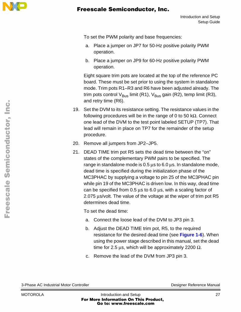
21. DEAD TIME trim pot R5 sets the dead time between the “on”states of the complementary PWM pairs to be specified. Therange in standalone mode is 0.5 µs to 6.0 µs. In standalone mode,dead time is specified during the initialization phase of theMC3PHAC by supplying a voltage to pin 25 of the MC3PHAC pinwhile pin 19 of the MC3PHAC is driven low. In this way, dead timecan be specified from 0.5 µs to 6.0 µs, with a scaling factor of2.075 µs/volt. The value of the voltage at the wiper of trim pot R5determines dead time.
To set the dead time:
a. Connect the loose lead of the DVM to JP3 pin 3.
b. Adjust the DEAD TIME trim pot, R5, to the requiredresistance for the desired dead time (see Figure 1-6). Whenusing the power stage described in this manual, set the deadtime for 2.5 µs, which will be approximately 2200 Ω.
c. Remove the lead of the DVM from JP3 pin 3.
3-Phase AC Industrial Motor Controller Designer Reference Manual
MOTOROLA Introduction and Setup 27 For More Information On This Product,
Go to: www.freescale.com

Introduction and Setup
F
ree
sca
le S
em
ico
nd
uc
tor,
I
Freescale Semiconductor, Inc.n
c..
.
Figure 1-6. Dead Time vs. Resistance
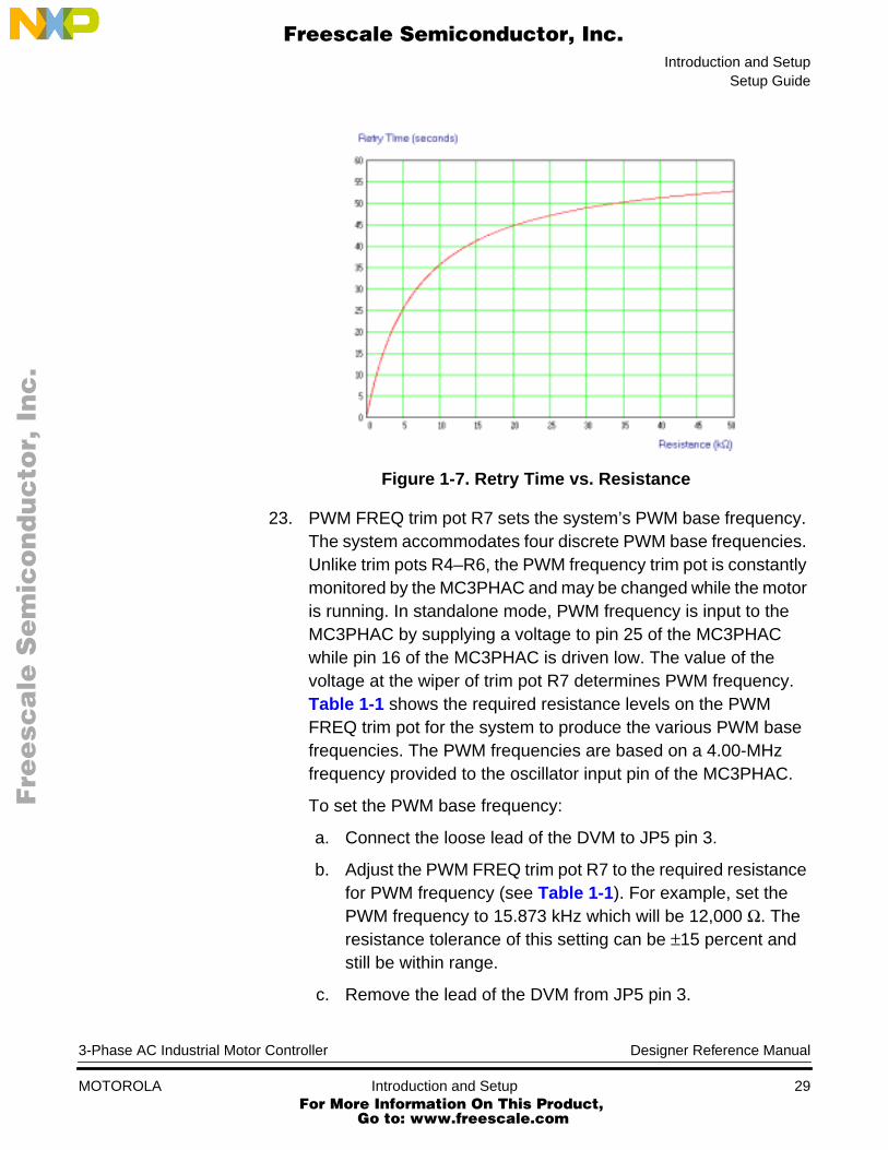
22. RETRY TIME trim pot R6 sets the time between a system faultbeing cleared and the time when the system will re-enable thePWM outputs. The retry time range in standalone mode is1 second to ~53 seconds. In standalone mode, retry time isspecified during the initialization phase of the MC3PHAC bysupplying a voltage to pin 25 of the MC3PHAC pin while pin 17 ofthe MC3PHAC is driven low. In this way, retry time can bespecified with a scaling factor of 12 sec/volt. The value of thevoltage at the wiper of trim pot R6 determines the retry time.
To set the retry time:
a. Connect the loose lead of the DVM to JP4 pin 3.
b. Adjust the RETRY TIME trim pot, R6, to the requiredresistance for the desired retry time (see Figure 1-7). Forexample, set the retry time to 15 seconds, which will beapproximately 2200 Ω.
c. Remove the lead of the DVM from JP4 pin 3.
Designer Reference Manual 3-Phase AC Industrial Motor Controller
28 Introduction and Setup MOTOROLA For More Information On This Product,
Go to: www.freescale.com
Introduction and SetupSetup Guide
F
ree
sca
le S
em
ico
nd
uc
tor,
I
Freescale Semiconductor, Inc.n
c..
.
Figure 1-7. Retry Time vs. Resistance
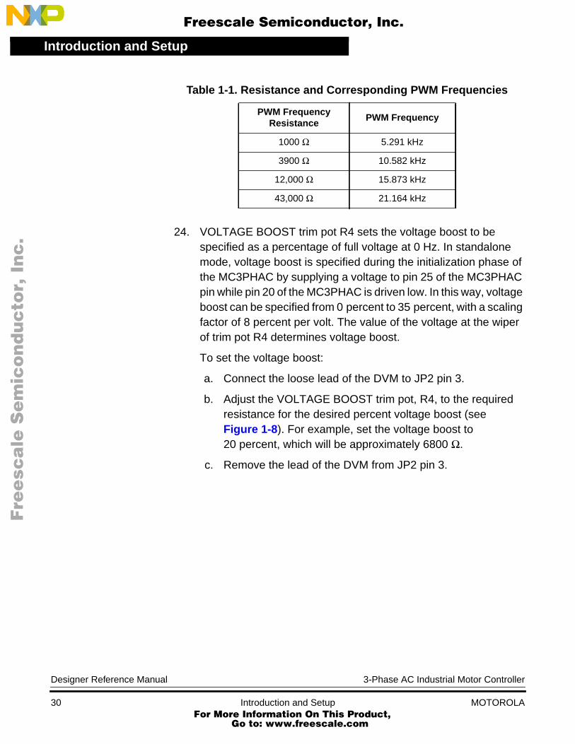
23. PWM FREQ trim pot R7 sets the system’s PWM base frequency.The system accommodates four discrete PWM base frequencies.Unlike trim pots R4–R6, the PWM frequency trim pot is constantlymonitored by the MC3PHAC and may be changed while the motoris running. In standalone mode, PWM frequency is input to theMC3PHAC by supplying a voltage to pin 25 of the MC3PHACwhile pin 16 of the MC3PHAC is driven low. The value of thevoltage at the wiper of trim pot R7 determines PWM frequency.Table 1-1 shows the required resistance levels on the PWMFREQ trim pot for the system to produce the various PWM basefrequencies. The PWM frequencies are based on a 4.00-MHzfrequency provided to the oscillator input pin of the MC3PHAC.
To set the PWM base frequency:
a. Connect the loose lead of the DVM to JP5 pin 3.
b. Adjust the PWM FREQ trim pot R7 to the required resistancefor PWM frequency (see Table 1-1). For example, set thePWM frequency to 15.873 kHz which will be 12,000 Ω. Theresistance tolerance of this setting can be ±15 percent andstill be within range.
c. Remove the lead of the DVM from JP5 pin 3.
3-Phase AC Industrial Motor Controller Designer Reference Manual
MOTOROLA Introduction and Setup 29 For More Information On This Product,
Go to: www.freescale.com
Introduction and Setup
F
ree
sca
le S
em
ico
nd
uc
tor,
I
Freescale Semiconductor, Inc.n
c..
.
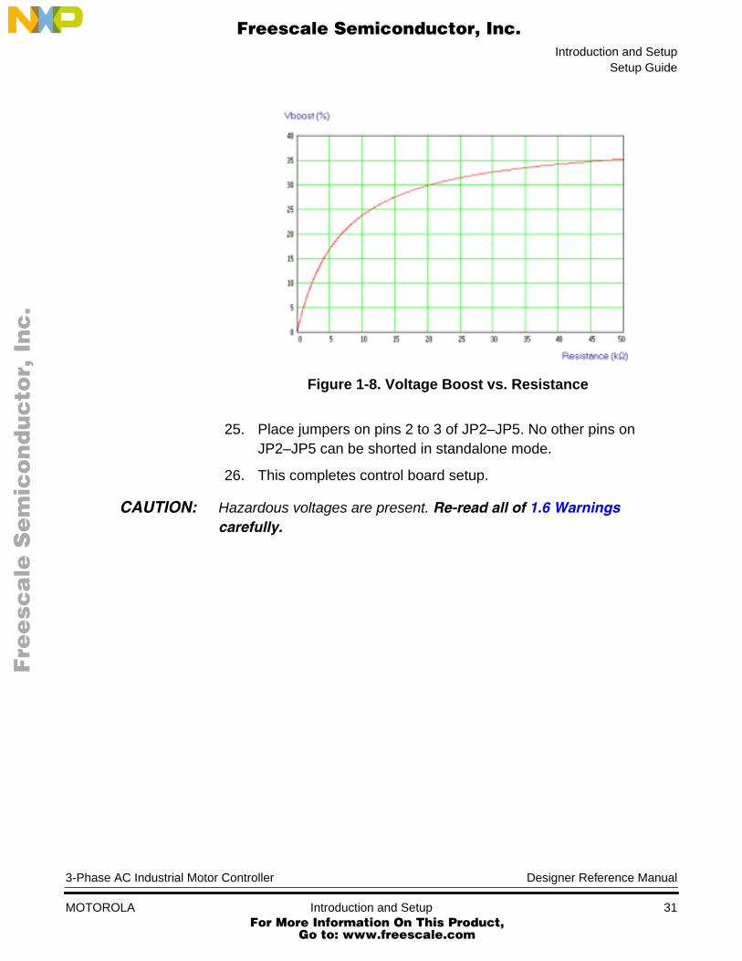
24. VOLTAGE BOOST trim pot R4 sets the voltage boost to bespecified as a percentage of full voltage at 0 Hz. In standalonemode, voltage boost is specified during the initialization phase ofthe MC3PHAC by supplying a voltage to pin 25 of the MC3PHACpin while pin 20 of the MC3PHAC is driven low. In this way, voltageboost can be specified from 0 percent to 35 percent, with a scalingfactor of 8 percent per volt. The value of the voltage at the wiperof trim pot R4 determines voltage boost.To set the voltage boost:
a. Connect the loose lead of the DVM to JP2 pin 3.
b. Adjust the VOLTAGE BOOST trim pot, R4, to the requiredresistance for the desired percent voltage boost (seeFigure 1-8). For example, set the voltage boost to20 percent, which will be approximately 6800 Ω.
c. Remove the lead of the DVM from JP2 pin 3.
Table 1-1. Resistance and Corresponding PWM Frequencies
PWM FrequencyResistance
PWM Frequency
1000 Ω 5.291 kHz
3900 Ω 10.582 kHz
12,000 Ω 15.873 kHz
43,000 Ω 21.164 kHz
Designer Reference Manual 3-Phase AC Industrial Motor Controller
30 Introduction and Setup MOTOROLA For More Information On This Product,
Go to: www.freescale.com
Introduction and SetupSetup Guide
F
ree
sca
le S
em
ico
nd
uc
tor,
I
Freescale Semiconductor, Inc.n
c..
.
Figure 1-8. Voltage Boost vs. Resistance
25. Place jumpers on pins 2 to 3 of JP2–JP5. No other pins onJP2–JP5 can be shorted in standalone mode.
26. This completes control board setup.
CAUTION: Hazardous voltages are present. Re-read all of 1.6 Warningscarefully.
3-Phase AC Industrial Motor Controller Designer Reference Manual
MOTOROLA Introduction and Setup 31 For More Information On This Product,
Go to: www.freescale.com

Introduction and Setup
F
ree
sca
le S
em
ico
nd
uc
tor,
I
Freescale Semiconductor, Inc.n
c..
.
Designer Reference Manual 3-Phase AC Industrial Motor Controller
32 Introduction and Setup MOTOROLA For More Information On This Product,
Go to: www.freescale.com
F
ree
sca
le S
em
ico
nd
uc
tor,
IFreescale Semiconductor, Inc.
nc
...
Designer Reference Manual — 3-Phase AC Industrial Motor Controller
Section 2. Operational Description
2.1 Contents
2.2 Introduction . . . . . . . . . . . . . . . . . . . . . . . . . . . . . . . . . . . . . . . .33
2.3 Electrical Characteristics . . . . . . . . . . . . . . . . . . . . . . . . . . . . .35
2.4 User Interfaces . . . . . . . . . . . . . . . . . . . . . . . . . . . . . . . . . . . . .352.4.1 Potentiometers . . . . . . . . . . . . . . . . . . . . . . . . . . . . . . . . . . .352.4.2 Switches . . . . . . . . . . . . . . . . . . . . . . . . . . . . . . . . . . . . . . . .372.4.3 Jumpers . . . . . . . . . . . . . . . . . . . . . . . . . . . . . . . . . . . . . . . .382.4.4 Indicator Lights . . . . . . . . . . . . . . . . . . . . . . . . . . . . . . . . . . .392.4.5 Test Points . . . . . . . . . . . . . . . . . . . . . . . . . . . . . . . . . . . . . .392.4.6 Optoisolated RS232 Interface . . . . . . . . . . . . . . . . . . . . . . .40
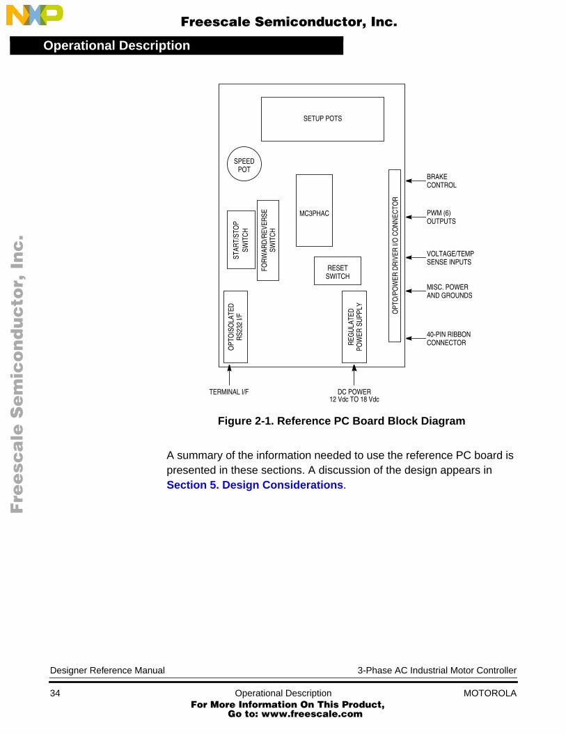
2.2 Introduction
The reference PC board, utilizing the MC3PHAC integrated circuit, isdesigned to provide control signals for 3-phase ac induction motors. Incombination with the embedded motion control series power stages andan optoisolation board, it provides a platform for evaluating theMC3PHAC.
User control inputs are accepted from START/STOP switches,FWD/REV switches, and a SPEED potentiometer located on thereference design PC board. Alternatively, motor commands can beentered via a PC and transmitted over a serial cable to DB-9 connectorJ2. Output connections and power stage feedback signals are groupedtogether on 40-pin ribbon cable connector J1. Power for operation of thereference PC board is supplied through the 40-pin ribbon cable from theoptoisolation board.
Figure 2-1 shows a block diagram of the reference board’s circuitry.
3-Phase AC Industrial Motor Controller Designer Reference Manual
MOTOROLA Operational Description 33 For More Information On This Product,
Go to: www.freescale.com
Operational Description
F
ree
sca
le S
em
ico
nd
uc
tor,
I
Freescale Semiconductor, Inc.n
c..
.
Figure 2-1. Reference PC Board Block Diagram
A summary of the information needed to use the reference PC board ispresented in these sections. A discussion of the design appears inSection 5. Design Considerations.
MC3PHAC
SETUP POTS
RESETSWITCH
OPT
O/P
OW
ER D
RIV
ER I/
O C
ON
NEC
TOR
REG
ULA
TED
POW
ER S
UPP
LY
SPEEDPOT
FOR
WAR
D/R
EVER
SESW
ITC
H
STAR
T/ST
OP
SWIT
CH
OPT
OIS
OLA
TED
RS2
32 I/
F
BRAKECONTROL
PWM (6)OUTPUTS
VOLTAGE/TEMPSENSE INPUTS
MISC. POWERAND GROUNDS
40-PIN RIBBONCONNECTOR
TERMINAL I/F DC POWER12 Vdc TO 18 Vdc
Designer Reference Manual 3-Phase AC Industrial Motor Controller
34 Operational Description MOTOROLA For More Information On This Product,
Go to: www.freescale.com
Operational DescriptionElectrical Characteristics
F
ree
sca
le S
em
ico
nd
uc
tor,
I
Freescale Semiconductor, Inc.n
c..
.
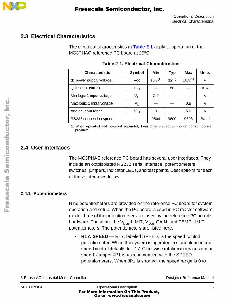
2.3 Electrical Characteristics
The electrical characteristics in Table 2-1 apply to operation of theMC3PHAC reference PC board at 25°C.
2.4 User Interfaces
The MC3PHAC reference PC board has several user interfaces. Theyinclude an optoisolated RS232 serial interface, potentiometers,switches, jumpers, indicator LEDs, and test points. Descriptions for eachof these interfaces follow.
2.4.1 Potentiometers
Nine potentiometers are provided on the reference PC board for systemoperation and setup. When the PC board is used in PC master softwaremode, three of the potentiometers are used by the reference PC board’shardware. These are the VBus LIMIT, VBus GAIN, and TEMP LIMITpotentiometers. The potentiometers are listed here.
• R17: SPEED — R17, labeled SPEED, is the speed controlpotentiometer. When the system is operated in standalone mode,speed control defaults to R17. Clockwise rotation increases motorspeed. Jumper JP1 is used in concert with the SPEEDpotentiometers. When JP1 is shorted, the speed range is 0 to
Table 2-1. Electrical Characteristics
Characteristic Symbol Min Typ Max Units
dc power supply voltage Vdc 10.8(1)
1. When operated and powered separately from other embedded motion control toolsetproducts
12(1) 16.5(1) V
Quiescent current ICC — 80 — mA
Min logic 1 input voltage VIH 2.0 — — V
Max logic 0 input voltage VIL — — 0.8 V
Analog input range VIN 0 — 5.0 V
RS232 connection speed — 9504 9600 9696 Baud
3-Phase AC Industrial Motor Controller Designer Reference Manual
MOTOROLA Operational Description 35 For More Information On This Product,
Go to: www.freescale.com
Operational Description
F
ree
sca
le S
em
ico
nd
uc
tor,
I
Freescale Semiconductor, Inc.n
c..
.
128 Hz. When JP1 is removed, the speed range is 0 to ~66 Hz.When operating in PC master software mode, speed controlcommands are sent over the RS232 interface. In PC mastersoftware mode, R17 may be monitored but its position has nocontrol over the motor. In future implementations of PC mastersoftware, R17 could be used to control the motor’s speed.
• R8: ACCEL — Acceleration control is set by trim potentiometerR8 (ACCEL). Clockwise rotation increases the motor’sacceleration rate.
• R1: VBus LIMIT — The overvoltage fault threshold is set by trimpotentiometer R1 (VBus LIMIT). Clockwise rotation increases thethreshold. R1 is used in concert with trim potentiometer R2, VBusGAIN.
• R2: VBus GAIN — The voltage bus gain trim potentiometer, R2(VBus GAIN), divides the high-voltage bus feedback that is inputfrom the optoisolator board or power board. Its output then drivesa gain-of-three amplifier which provides a bus voltagerepresentation to the MC3PHAC and also drives the overvoltagefault input. Clockwise rotation increases gain.
• R3: TEMP LIMIT — The high-temperature fault threshold is set bytrim potentiometer R3 (TEMP LIMIT). Clockwise rotationincreases the high-temperature threshold fault point.
• R4: VOLTAGE BOOST — The voltage boost trim potentiometer,R4 (VOLTAGE BOOST), is used as an input to the MC3PHAC. Itsets the low-frequency voltage boost characteristic. Clockwiserotation increases voltage boost.
• R5: DEAD TIME — The dead time trim potentiometer, R5 (DEADTIME), is used to set the complementary top-to-bottom transitiondelay time. The range of dead time in standalone operation is0.5 µs to 6.0 µs. Clockwise rotation increases dead time.
• R6: RETRY TIME — The retry time trim potentiometer, R6(RETRY TIME), sets the time between a system fault beingcleared and the time when the system will re-enable the PWMoutputs. Retry range in standalone mode is 1 second to~53 seconds. Clockwise rotation increases fault retry time.
Designer Reference Manual 3-Phase AC Industrial Motor Controller
36 Operational Description MOTOROLA For More Information On This Product,
Go to: www.freescale.com
Operational DescriptionUser Interfaces
F
ree
sca
le S
em
ico
nd
uc
tor,
I
Freescale Semiconductor, Inc.n
c..
.
• R7: PWM FREQ — The PWM frequency trim potentiometer setsthe PWM frequency. Depending on the position of the trimpotentiometer, the PWM frequency choices are 5.291 kHz,10.582 kHz, 15.873 kHz, and 21.164 kHz. Clockwise rotationincreases PWM frequency.
2.4.2 Switches
Three switches provide for user inputs. They are listed here.
• SW1: START/STOP — SW1, START/STOP, is a toggle switchlocated on the left-hand side of the board. It starts and stops themotor when the system is operated in standalone mode. Switchingit up (toward the top of the board) turns the motor on, andswitching it down stops it. In PC master software mode, theSTART/STOP switch may be monitored, but its position has nocontrol over the motor. In future implementations of PC mastersoftware, SW1 could be used to start or stop the motor.
• SW2: FWD/REV — SW2, FWD/REV, is a toggle switch located tothe right of the START/STOP. It controls direction of the motorwhen the system is operated in standalone mode. Positioning it up(toward the top of the board) runs the motor forward; switching itdown runs it in reverse. In PC master software mode, theFWD/REV switch may be monitored, but its position has no controlover the motor. In future implementations of PC master software,SW2 could be used to change direction of the motor.
• SW3: RESET — SW3, the RESET switch, is a push buttonlocated near the lower center of the board. It resets the MC3PHACin standalone and PC master software modes.
3-Phase AC Industrial Motor Controller Designer Reference Manual
MOTOROLA Operational Description 37 For More Information On This Product,
Go to: www.freescale.com
Operational Description
F
ree
sca
le S
em
ico
nd
uc
tor,
I
Freescale Semiconductor, Inc.n
c..
.
2.4.3 Jumpers
There are 10 jumpers: JP1–JP10. Jumper JP1 is located on theupper-left corner of the PC board, just above the SPEEDpotentiometers. JP2 through JP5 are grouped near the upper center ofthe PC board. JP6 through JP9 are located above and to the right of theFWD/REV switch. JP10 is located near the bottom right-hand side of thePC board and to the left of the 40-pin ribbon cable connector. They aredescribed here.
• JP1 — Jumper JP1 is used to set the frequency range of the sixPWM outputs. When JP1 is shorted, the speed range is 0 to128 Hz. When JP1 is removed, the speed range is 0 to ~66 Hz.
• JP2 — Jumper JP2 is a 4-position jumper header. When shortedbetween positions 1 and 2, the MC3PHAC is set to run in PCmaster software mode. When shorted between positions 2 and 3,the MC3PHAC is set to run in standalone mode. In standalonemode, the voltage boost trim potentiometer is connected to theMC3PHAC’s pin 20. Positions 3 and 4 are unused.
• JP3 — Jumper JP3 is a 4-position jumper header. When shortedbetween positions 1 and 2, the MC3PHAC is set to run in PCmaster software mode and the fault LED is connected to theMC3PHAC’s fault output. When shorted between positions 2 and3, the MC3PHAC is set to run in standalone mode. In standalonemode, the dead time trim potentiometer is connected to theMC3PHAC’s pin 19. Positions 3 and 4 are unused.
• JP4 — Jumper JP4 is a 4-position jumper header. When shortedbetween positions 1 and 2, the MC3PHAC is set to run in PCmaster software mode and the serial output of the MC3PHAC isconnected to the optoisolated RS232 transmit optoisolator. Whenshorted between positions 2 and 3, the MC3PHAC is set to run instandalone mode. In standalone mode, the retry time trimpotentiometer is connected to the MC3PHAC’s pin 17. Positions 3and 4 are unused.
• JP5 — Jumper JP5 is a 4-position jumper header. When shortedbetween positions 1 and 2, the MC3PHAC is set to run in PCmaster software mode and the serial input of the MC3PHAC isconnected to the optoisolated RS232 receive optoisolator. When
Designer Reference Manual 3-Phase AC Industrial Motor Controller
38 Operational Description MOTOROLA For More Information On This Product,
Go to: www.freescale.com

Operational DescriptionUser Interfaces
F
ree
sca
le S
em
ico
nd
uc
tor,
I
Freescale Semiconductor, Inc.n
c..
.
JP5 is shorted between positions 2 and 3, the MC3PHAC is set torun in standalone mode. In standalone mode, the PWM frequencytrim potentiometer is connected to the MC3PHAC’s pin 18.Positions 3 and 4 are unused.
• JP6 through JP9 — Jumpers JP6 through JP9 are 2-positionjumper headers. Only one of these jumpers may be installed atany given time. The jumpers set the PWM frequency at 50 Hz or60 Hz, positive or negative PWM polarity. Only jumper blocks JP7and JP9 are populated on the PC board.
• JP10 — Jumper JP10 is used to prevent ground loops when theanalog ground reference originates on an external PC board, as inthe case with the optoisolation PC board. In normal operation, thisjumper is removed. JP10 is installed if the reference PC board isself-powered and running without a power module or optoisolationboard connected to J1.
2.4.4 Indicator Lights
Three LEDs located on the control board provide status information tothe user. The power-on LED, D6, is located to the right of the FWD/REVswitch. The fault LED, D1, is located just above and to the right of theSPEED potentiometers. The brake LED, D2, is located to the right of thefault LED. Descriptions are listed here.
• D1: Fault (Red) — D1 illuminates when a fault has occurred.
• D2: Brake (Yellow) — D2 illuminates when the MC3PHACenergizes the resistive brake.
• D6: Power On — D6, labeled POWER, illuminates when power isapplied to the board.
2.4.5 Test Points
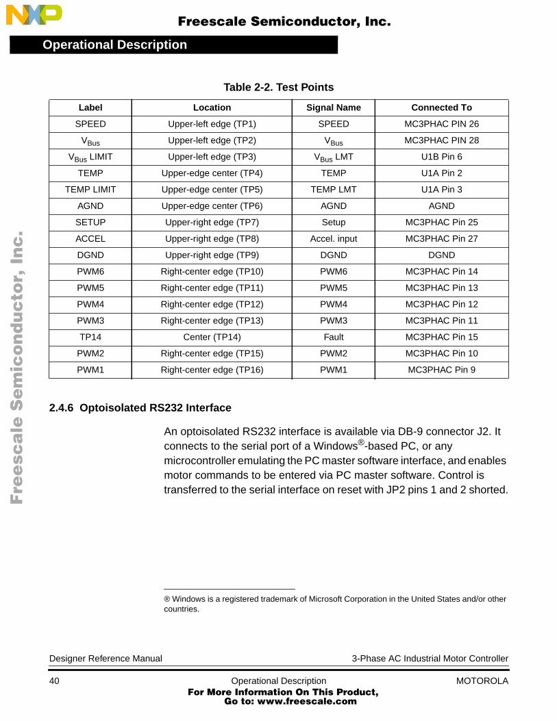
A variety of test points are provided to facilitate measurements with aDVM or an oscilloscope. They are listed in Table 2-2.
3-Phase AC Industrial Motor Controller Designer Reference Manual
MOTOROLA Operational Description 39 For More Information On This Product,
Go to: www.freescale.com
Operational Description
F
ree
sca
le S
em
ico
nd
uc
tor,
I
Freescale Semiconductor, Inc.n
c..
.
2.4.6 Optoisolated RS232 Interface
An optoisolated RS232 interface is available via DB-9 connector J2. Itconnects to the serial port of a Windows®-based PC, or anymicrocontroller emulating the PC master software interface, and enablesmotor commands to be entered via PC master software. Control istransferred to the serial interface on reset with JP2 pins 1 and 2 shorted.
® Windows is a registered trademark of Microsoft Corporation in the United States and/or othercountries.
Table 2-2. Test Points
Label Location Signal Name Connected To
SPEED Upper-left edge (TP1) SPEED MC3PHAC PIN 26
VBus Upper-left edge (TP2) VBus MC3PHAC PIN 28
VBus LIMIT Upper-left edge (TP3) VBus LMT U1B Pin 6
TEMP Upper-edge center (TP4) TEMP U1A Pin 2
TEMP LIMIT Upper-edge center (TP5) TEMP LMT U1A Pin 3
AGND Upper-edge center (TP6) AGND AGND
SETUP Upper-right edge (TP7) Setup MC3PHAC Pin 25
ACCEL Upper-right edge (TP8) Accel. input MC3PHAC Pin 27
DGND Upper-right edge (TP9) DGND DGND
PWM6 Right-center edge (TP10) PWM6 MC3PHAC Pin 14
PWM5 Right-center edge (TP11) PWM5 MC3PHAC Pin 13
PWM4 Right-center edge (TP12) PWM4 MC3PHAC Pin 12
PWM3 Right-center edge (TP13) PWM3 MC3PHAC Pin 11
TP14 Center (TP14) Fault MC3PHAC Pin 15
PWM2 Right-center edge (TP15) PWM2 MC3PHAC Pin 10
PWM1 Right-center edge (TP16) PWM1 MC3PHAC Pin 9
Designer Reference Manual 3-Phase AC Industrial Motor Controller
40 Operational Description MOTOROLA For More Information On This Product,
Go to: www.freescale.com
F
ree
sca
le S
em
ico
nd
uc
tor,
IFreescale Semiconductor, Inc.
nc
...
Designer Reference Manual — 3-Phase AC Industrial Motor Controller
Section 3. Pin Descriptions
3.1 Contents
3.2 Introduction . . . . . . . . . . . . . . . . . . . . . . . . . . . . . . . . . . . . . . . .41
3.3 Control Board Signal Descriptions . . . . . . . . . . . . . . . . . . . . . .413.3.1 40-Pin Connector J1. . . . . . . . . . . . . . . . . . . . . . . . . . . . . . .413.3.2 Optoisolated RS232 DB-9 Connector J2 . . . . . . . . . . . . . . .453.3.3 Power Connector J3. . . . . . . . . . . . . . . . . . . . . . . . . . . . . . .45
3.2 Introduction
Three connectors are resident on the control board, labeled J1 throughJ3. They are:
• J1 — 40-pin ribbon cable connector
• J2 — RS232 DB-9 connector
• J3 — Power jack
3.3 Control Board Signal Descriptions
The following subsections describe signals on control board connectorsJ1 through J3.
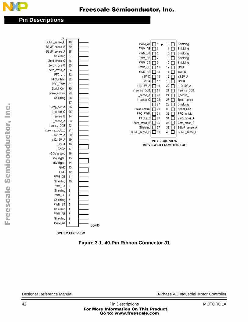
3.3.1 40-Pin Connector J1
Signals to and from an optoisolation board or power stage are groupedtogether on 40-pin ribbon cable connector J1. Pin assignments areshown in Figure 3-1. In this figure, a schematic representation appearson the left, and a physical layout of the connector appears on the right.Pin descriptions are listed in Table 3-1.
3-Phase AC Industrial Motor Controller Designer Reference Manual
MOTOROLA Pin Descriptions 41 For More Information On This Product,
Go to: www.freescale.com
Pin Descriptions
F
ree
sca
le S
em
ico
nd
uc
tor,
I
Freescale Semiconductor, Inc.n
c..
.
Figure 3-1. 40-Pin Ribbon Connector J1
40393837363534333231302928272625242322212019181716151413121110987654321
BEMF_sense_CBEMF_sense_BBEMF_sense_A
ShieldingZero_cross_CZero_cross_BZero_cross_A
PFC_z_cPFC_inhibitPFC_PWMSerial_Con
Brake_controlShielding
Temp_senseI_sense_CI_sense_BI_sense_A
I_sense_DCBV_sense_DCB_5
–12/15V_A+12/15V_A
GNDAGNDA
+3.3V analog+5V digital+5V digital
GNDGND
PWM_CBShieldingPWM_CTShieldingPWM_BBShieldingPWM_BTShieldingPWM_ABShieldingPWM_AT
SCHEMATIC VIEW
J5
2468
10121416182022242628303234363840
13579111315171921232527293133353739
ShieldingShieldingShieldingShieldingShieldingGND+5V_D+3.3V_AGNDA–12/15V_AI_sense_DCBI_sense_BTemp_senseShieldingSerial_ConPFC_inhibitZero_cross_AZero_cross_CBEMF_sense_ABEMF_sense_C
PWM_ATPWM_ABPWM_BTPWM_BBPWM_CTPWM_CBGND_PS
+5V_DGNDA
+12/15V_AV_sense_DCB
I_sense_AI_sense_C
Brake controlPFC_PWM
PFC_z_cZero_cross_B
ShieldingBEMF_sense_B
PHYSICAL VIEWAS VIEWED FROM THE TOP
CON40
Designer Reference Manual 3-Phase AC Industrial Motor Controller
42 Pin Descriptions MOTOROLA For More Information On This Product,
Go to: www.freescale.com

Pin DescriptionsControl Board Signal Descriptions
F
ree
sca
le S
em
ico
nd
uc
tor,
I
Freescale Semiconductor, Inc.n
c..
.
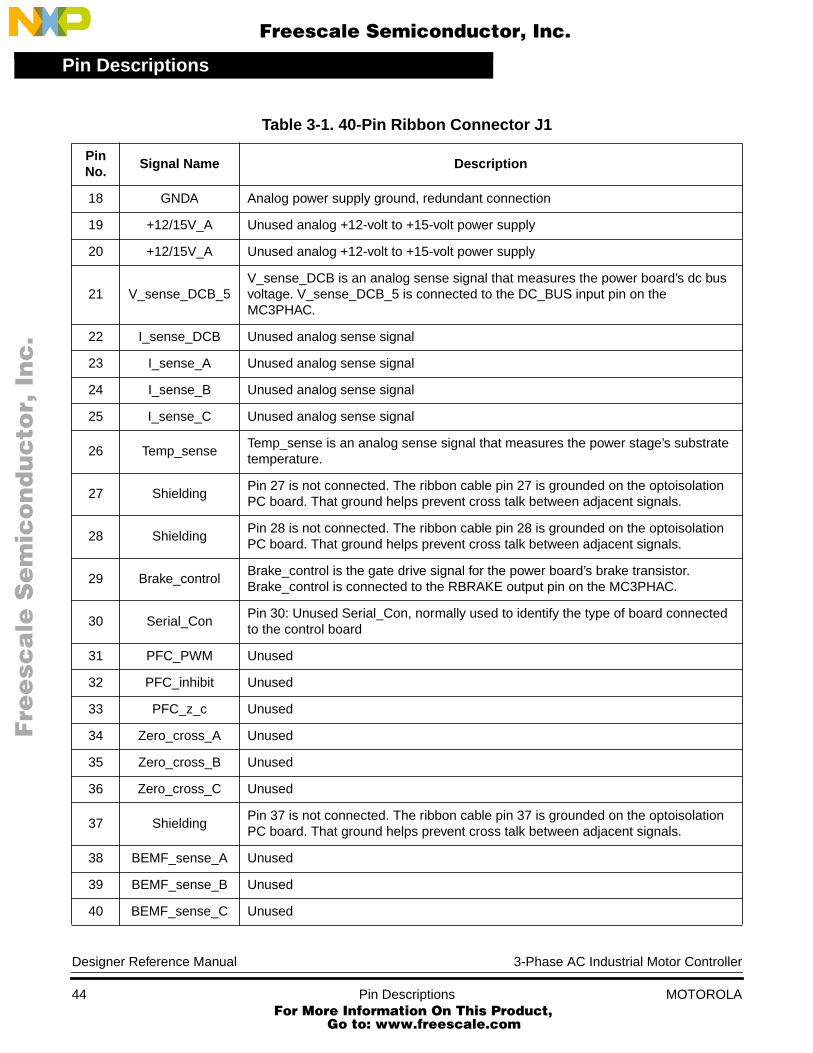
Table 3-1. 40-Pin Ribbon Connector J1
PinNo.
Signal Name Description
1 PWM_ATPWM_AT is the gate drive signal for the top half-bridge of phase A. A logic highturns phase A’s top switch on. PWM_AT is connected to PWM_U_TOP on theMC3PHAC.
2 ShieldingPin 2 is not connected. The ribbon cable pin 2 is grounded on the optoisolation PCboard. That ground helps prevent cross talk between adjacent signals.
3 PWM_ABPWM_AB is the gate drive signal for the bottom half-bridge of phase A. A logic highturns phase A’s bottom switch on. PWM_AB is connected to PWM_U_BOP on theMC3PHAC.
4 ShieldingPin 4 is not connected. The ribbon cable pin 4 is grounded on the optoisolation PCboard. That ground helps prevent cross talk between adjacent signals.
5 PWM_BTPWM_BT is the gate drive signal for the top half-bridge of phase B. A logic highturns phase B’s top switch on. PWM_BT is connected to PWM_V_TOP on theMC3PHAC.
6 ShieldingPin 6 is not connected. The ribbon cable pin 6 is grounded on the optoisolation PCboard. That ground helps prevent cross talk between adjacent signals.
7 PWM_BBPWM_BB is the gate drive signal for the bottom half-bridge of phase B. A logic highturns phase B’s bottom switch on. PWM_BB is connected to PWM_V_BOT on theMC3PHAC.
8 ShieldingPin 8 is not connected. The ribbon cable pin 8 is grounded on the optoisolation PCboard. That ground helps prevent cross talk between adjacent signals.
9 PWM_CTPWM_CT is the gate drive signal for the top half-bridge of phase C. A logic highturns phase C’s top switch on. PWM_CT is connected to PWM_W_TOP on theMC3PHAC.
10 ShieldingPin 10 is not connected. The ribbon cable pin 10 is grounded on the optoisolationPC board. That ground helps prevent cross talk between adjacent signals.
11 PWM_CBPWM_CB is the gate drive signal for the bottom half-bridge of phase C. A logic highturns phase C’s bottom switch on. PWM_CB is connected to PWM_W_BOT on theMC3PHAC.
12 GND Digital power supply ground
13 GND Digital power supply ground, redundant connection
14 +5V_D Digital +5-volt power supply
15 +5V digital Digital +5-volt power supply, redundant connection
16 +3.3V analog Unused
17 GNDA Analog power supply ground
3-Phase AC Industrial Motor Controller Designer Reference Manual
MOTOROLA Pin Descriptions 43 For More Information On This Product,
Go to: www.freescale.com
Pin Descriptions
F
ree
sca
le S
em
ico
nd
uc
tor,
I
Freescale Semiconductor, Inc.n
c..
.
18 GNDA Analog power supply ground, redundant connection
19 +12/15V_A Unused analog +12-volt to +15-volt power supply
20 +12/15V_A Unused analog +12-volt to +15-volt power supply
21 V_sense_DCB_5V_sense_DCB is an analog sense signal that measures the power board’s dc busvoltage. V_sense_DCB_5 is connected to the DC_BUS input pin on theMC3PHAC.
22 I_sense_DCB Unused analog sense signal
23 I_sense_A Unused analog sense signal
24 I_sense_B Unused analog sense signal
25 I_sense_C Unused analog sense signal
26 Temp_senseTemp_sense is an analog sense signal that measures the power stage’s substratetemperature.
27 ShieldingPin 27 is not connected. The ribbon cable pin 27 is grounded on the optoisolationPC board. That ground helps prevent cross talk between adjacent signals.
28 ShieldingPin 28 is not connected. The ribbon cable pin 28 is grounded on the optoisolationPC board. That ground helps prevent cross talk between adjacent signals.
29 Brake_controlBrake_control is the gate drive signal for the power board’s brake transistor.Brake_control is connected to the RBRAKE output pin on the MC3PHAC.
30 Serial_ConPin 30: Unused Serial_Con, normally used to identify the type of board connectedto the control board
31 PFC_PWM Unused
32 PFC_inhibit Unused
33 PFC_z_c Unused
34 Zero_cross_A Unused
35 Zero_cross_B Unused
36 Zero_cross_C Unused
37 ShieldingPin 37 is not connected. The ribbon cable pin 37 is grounded on the optoisolationPC board. That ground helps prevent cross talk between adjacent signals.
38 BEMF_sense_A Unused
39 BEMF_sense_B Unused
40 BEMF_sense_C Unused
Table 3-1. 40-Pin Ribbon Connector J1
PinNo.
Signal Name Description
Designer Reference Manual 3-Phase AC Industrial Motor Controller
44 Pin Descriptions MOTOROLA For More Information On This Product,
Go to: www.freescale.com
Pin DescriptionsControl Board Signal Descriptions
F
ree
sca
le S
em
ico
nd
uc
tor,
I
Freescale Semiconductor, Inc.n
c..
.
3.3.2 Optoisolated RS232 DB-9 Connector J2
The RS232 DB-9 connector, J2, is a 9-pin female connector for serialcommunications with a PC. It has standard RS232 pinouts. Theschematic Figure 4-3 shows J2 at the top-center of the page. Pinoutsare listed in Table 3-2.
3.3.3 Power Connector J3
A power connector, J3, is a 2.1-mm power jack that provides connectionto a 12-volt dc power supply. This power input connector is used onlywhen the control board is operating independently from other boards inthe embedded motion control toolset.
Table 3-2. Optoisolated RS232 DB-9 Connector J2
PinNo.
Signal Name Description
1 Unused N/A
2 RXD Data received by the PC from the control board
3 TXD Data transmitted from the PC to the control board
4 DTR PC indicates that it is ready to receive data.
5 GND Common ground reference
6 Unused N/A
7 RTS PC requests to send data to the control board.
8 Unused N/A
9 Unused N/A
3-Phase AC Industrial Motor Controller Designer Reference Manual
MOTOROLA Pin Descriptions 45 For More Information On This Product,
Go to: www.freescale.com

Pin Descriptions
F
ree
sca
le S
em
ico
nd
uc
tor,
I
Freescale Semiconductor, Inc.n
c..
.
Designer Reference Manual 3-Phase AC Industrial Motor Controller
46 Pin Descriptions MOTOROLA For More Information On This Product,
Go to: www.freescale.com
F
ree
sca
le S
em
ico
nd
uc
tor,
IFreescale Semiconductor, Inc.
nc
...
Designer Reference Manual — 3-Phase AC Industrial Motor Controller
Section 4. Schematics and Parts List
4.1 Contents
4.2 Schematics . . . . . . . . . . . . . . . . . . . . . . . . . . . . . . . . . . . . . . . .47
4.3 Parts Lists . . . . . . . . . . . . . . . . . . . . . . . . . . . . . . . . . . . . . . . . .51
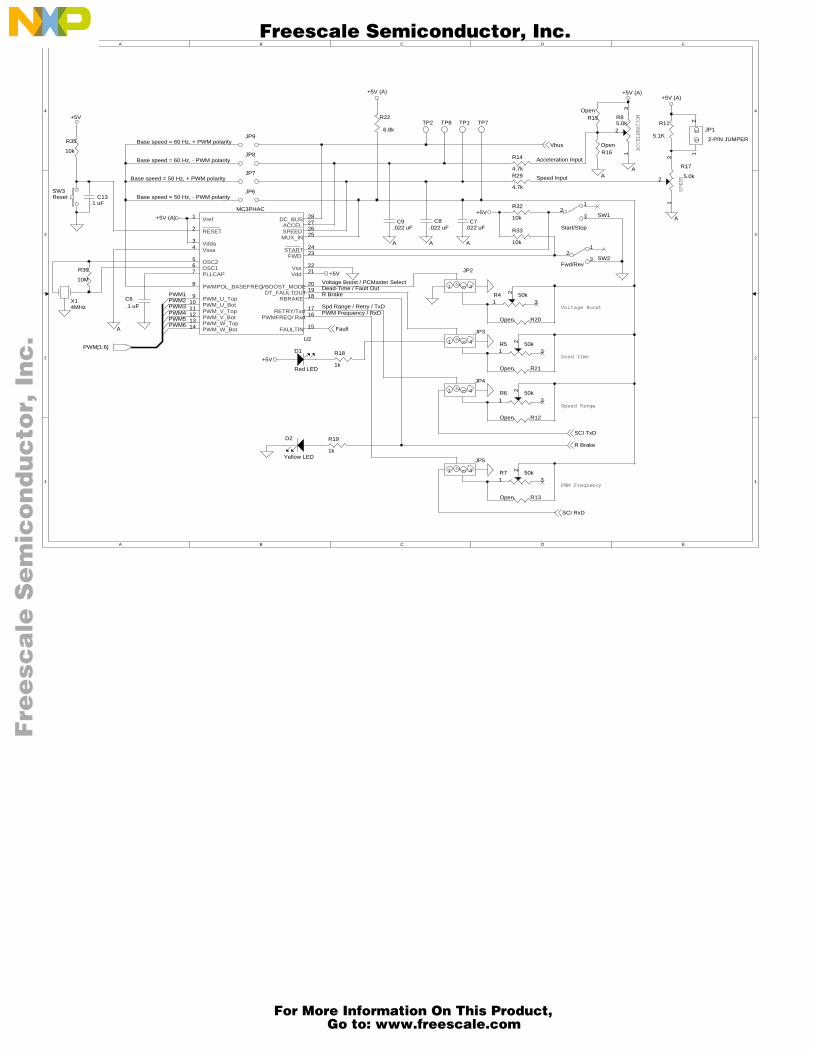
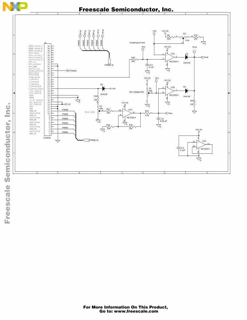
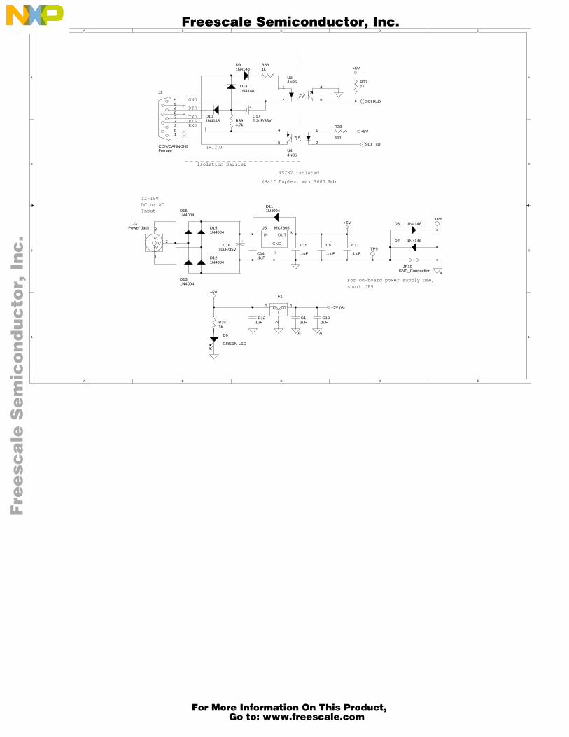
4.2 Schematics
A set of schematics for the reference PC board appears in Figure 4-1through Figure 4-3. Unless otherwise specified, resistors are 1/4 watt,have a ±5 percent tolerance, and have values shown in ohms.Interrupted lines coded with the same letters are electrically connected.
3-Phase AC Industrial Motor Controller Designer Reference Manual
MOTOROLA Schematics and Parts List 47 For More Information On This Product,
Go to: www.freescale.com
A B C D E
4 4
3 3
2 2
1 1
+5V (A)+5V (A)+5V (A)
SWRe
F
ree
sca
le S
em
ico
nd
uc
tor,
I
Freescale Semiconductor, Inc.n
c..
.
A B C D E
SPEED
ACCELERATION
PWM Frequency
Dead Time
Speed Range
Voltage Boost
Dead-Time / Fault Out
Base speed = 60 Hz, - PWM polarity
Spd Range / Retry / TxDPWM Frequency / RxD
Base speed = 50 Hz, - PWM polarity
Base speed = 50 Hz, + PWM polarity
Acceleration Input
Base speed = 60 Hz, + PWM polarity
PWM4
PWM6PWM5
PWM2PWM1
PWM3
Speed Input
Voltage Boost / PCMaster Select
R Brake
R Brake
Fault
Vbus
SCI TxD
SCI RxD
A
A
A
+5V
+5V (A)
A
+5V
A
+5V
A
+5V
A
JP4
1 2 3 4
JP5
1 2 3 4
JP1
2-PIN JUMPER
12
12
X14MHz
JP7
JP8
JP9
R11
5.1K
D1
Red LED
R4 50k1 3
2
R85.0k
13
2
R7 50k1 3
2
JP3
1 2 3 4
JP6
R16Open
C9.022 uF
C8.022 uF
SW2Fwd/Rev
21
3
C7.022 uF
R15Open
D2
Yellow LED
TP2
R19
1k
R20Open
TP8 TP1
R32
10k
TP7
R13Open
MC3PHAC
U2
65
2
8
25262728
1617
181920
2324
15
91011121314
2122
1
7
43
OSC1OSC2
RESET
PWMPOL_BASEFREQ
MUX_INSPEEDACCEL
DC_BUS
PWMFREQ/ RxdRETRY/Txd
RBRAKEDT_FAULTOUT
VBOOST_MODE
FWDSTART
FAULTIN
PWM_U_TopPWM_U_BotPWM_V_TopPWM_V_BotPWM_W_TopPWM_W_Bot
VddVss
Vref
PLLCAP
VssaVdda
R35
10k
R12Open
R21Open
R22
6.8k
R14
4.7kR29
4.7k
R33
10k
SW1
Start/Stop
21
3
R18
1k
3set
R30
10M
C13.1 uF
R17
5.0k
13
2
R5 50k1 3
2
R6 50k1 3
2
C6.1 uF
JP2
1 2 3 4
PWM[1:6]
For More Information On This Product,
Go to: www.freescale.com
A B C D E
4
3
2
1
+5V (A)TP515 111316 1012
F
ree
sca
le S
em
ico
nd
uc
tor,
I
Freescale Semiconductor, Inc.n
c..
.
A B C D E
4
3
2
1
PFC_PWM
Zero_cross_B
V_sense_DCB_5I_sense_DCB
+15V analog
BEMF_sense_B
PWM_BT
I_sense_B
Zero_cross_C
Serial_Con
Sheilding
Sheilding
I_sense_C
Sheilding
GNDPWM_CB
Sheilding
BEMF_sense_C
PFC_z_cPFC_inhibit
PWM_BB
BEMF_sense_A
Sheilding
GND
Temp_sense
Zero_cross_A
PWM_CT
Sheilding
GNDA
+3.3V analog+5V digital
GNDA
PWM_AT
Sheilding
-15V analog
+5V digital
PWM_AB
I_sense_A
Brake_control
Sheilding
Temperature limit
Bus voltage limit
VBUS GAIN
PWM1
PWM3
PWM2
PWM5
PWM4
PWM6
PW
M3
PW
M4
PW
M5
PW
M1
PW
M2
PW
M6
Fault
Vbus
R Brake
A
A
+5V (A)
A
+5V
A
+5V (A)
A
A
A
A
+5V
A
+5V (A)
+5V (A)
A
+5V (A)
A
TP
R23
10K
D3
1N4148
+
-
U1D
MC3320 4
12
1314
411
+
-
U1C
MC3320 4
10
98
411
+
-
U1B
MC3320 4
5
67
411
+
-
U1A
MC3320 4
3
21
411
R31
10K
R25
22K
R250k
13
2
R26
22K
R3
5.0k
1 3
2
TP
R9
22K
J1
CON/40
123456789
10111213141516171819202122232425262728293031323334353637383940
R10
15K
R28
10K
TPR150k
13
2
C30.1uF
TP4
TP
C40.1uF
D5
1N4148
R27
10K
C24700 pF
TP
R24
3.3k
TP14
TP3
TP
D4
1N4148
PWM[1:6]
PWM[1:6]
For More Information On This Product,
Go to: www.freescale.com
A B C D E
4 4
3 3
2 2
1 1
+5VR361k
D91N4148
F
ree
sca
le S
em
ico
nd
uc
tor,
I
Freescale Semiconductor, Inc.n
c..
.
A B C D E
For on-board power supply use,short JP9
RS232 isolated
12-15V DC or ACInput
(+12V)
GND
TXD
RXDRTS
DTR
(Half Duplex, max 9600 Bd)
Isolation Barrier
Female
SCI TxD
SCI RxD
AA
+5V (A)
A
+5V
+5V
+5V
D111N4004
+C16
10uF/35V
TP6
+
C172.2uF/35V
C15
.1uFC14.1uF
D7 1N4148
D6
GREEN LED
D8 1N4148J3Power Jack
1
2
3
+V-V
-V
D131N4004
J2
CON/CANNON9
594837261
D151N4004
D161N4004
D121N4004
R371k
R38
330
U5 MC78051 3
2
IN OUT
GND
D101N4148
R341k
F1
13
2
JP10GND_Connection
C5
.1 uF
C11
.1 uF
U44N35
14
25
TP9
U34N35
1 4
2 5
R394.7k
C121uF
C11uF
C10.1uF
D141N4148
For More Information On This Product,
Go to: www.freescale.com
Schematics and Parts ListParts Lists
F
ree
sca
le S
em
ico
nd
uc
tor,
I
Freescale Semiconductor, Inc.n
c..
.
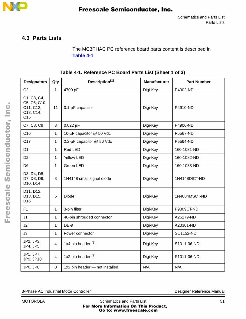
4.3 Parts Lists
The MC3PHAC PC reference board parts content is described inTable 4-1.
Table 4-1. Reference PC Board Parts List (Sheet 1 of 3)
Designators Qty Description(1) Manufacturer Part Number
C2 1 4700 pF Digi-Key P4902-ND
C1, C3, C4,C5, C6, C10,C11, C12,C13, C14,C15
11 0.1-µF capacitor Digi-Key P4910-ND
C7, C8, C9 3 0.022 µF Digi-Key P4906-ND
C16 1 10-µF capacitor @ 50 Vdc Digi-Key P5567-ND
C17 1 2.2-µF capacitor @ 50 Vdc Digi-Key P5564-ND
D1 1 Red LED Digi-Key 160-1081-ND
D2 1 Yellow LED Digi-Key 160-1082-ND
D6 1 Green LED Digi-Key 160-1083-ND
D3, D4, D5,D7, D8, D9,D10, D14
8 1N4148 small signal diode Digi-Key 1N4148DICT-ND
D11, D12,D13, D15,D16
5 Diode Digi-Key 1N4004MSCT-ND
F1 1 3-pin filter Digi-Key P9809CT-ND
J1 1 40-pin shrouded connector Digi-Key A26279-ND
J2 1 DB-9 Digi-Key A23301-ND
J3 1 Power connector Digi-Key SC1152-ND
JP2, JP3,JP4, JP5
4 1x4 pin header (2) Digi-Key S1011-36-ND
JP1, JP7,JP9, JP10
4 1x2 pin header (2) Digi-Key S1011-36-ND
JP6, JP8 0 1x2 pin header — not installed N/A N/A
3-Phase AC Industrial Motor Controller Designer Reference Manual
MOTOROLA Schematics and Parts List 51 For More Information On This Product,
Go to: www.freescale.com
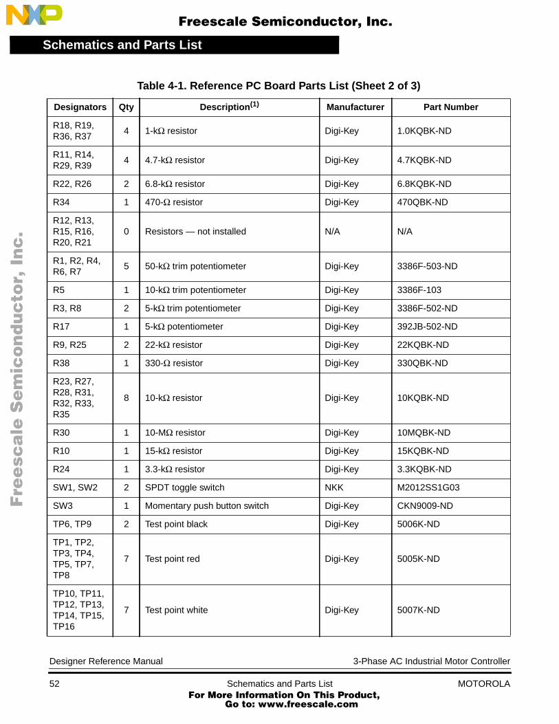
Schematics and Parts List
F
ree
sca
le S
em
ico
nd
uc
tor,
I
Freescale Semiconductor, Inc.n
c..
.
R18, R19,R36, R37
4 1-kΩ resistor Digi-Key 1.0KQBK-ND
R11, R14,R29, R39
4 4.7-kΩ resistor Digi-Key 4.7KQBK-ND
R22, R26 2 6.8-kΩ resistor Digi-Key 6.8KQBK-ND
R34 1 470-Ω resistor Digi-Key 470QBK-ND
R12, R13,R15, R16,R20, R21
0 Resistors — not installed N/A N/A
R1, R2, R4,R6, R7
5 50-kΩ trim potentiometer Digi-Key 3386F-503-ND
R5 1 10-kΩ trim potentiometer Digi-Key 3386F-103
R3, R8 2 5-kΩ trim potentiometer Digi-Key 3386F-502-ND
R17 1 5-kΩ potentiometer Digi-Key 392JB-502-ND
R9, R25 2 22-kΩ resistor Digi-Key 22KQBK-ND
R38 1 330-Ω resistor Digi-Key 330QBK-ND
R23, R27,R28, R31,R32, R33,R35
8 10-kΩ resistor Digi-Key 10KQBK-ND
R30 1 10-MΩ resistor Digi-Key 10MQBK-ND
R10 1 15-kΩ resistor Digi-Key 15KQBK-ND
R24 1 3.3-kΩ resistor Digi-Key 3.3KQBK-ND
SW1, SW2 2 SPDT toggle switch NKK M2012SS1G03
SW3 1 Momentary push button switch Digi-Key CKN9009-ND
TP6, TP9 2 Test point black Digi-Key 5006K-ND
TP1, TP2,TP3, TP4,TP5, TP7,TP8
7 Test point red Digi-Key 5005K-ND
TP10, TP11,TP12, TP13,TP14, TP15,TP16
7 Test point white Digi-Key 5007K-ND
Table 4-1. Reference PC Board Parts List (Sheet 2 of 3)
Designators Qty Description(1) Manufacturer Part Number
Designer Reference Manual 3-Phase AC Industrial Motor Controller
52 Schematics and Parts List MOTOROLA For More Information On This Product,
Go to: www.freescale.com
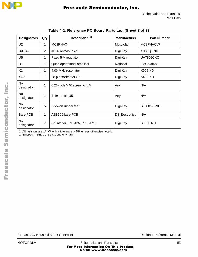
Schematics and Parts ListParts Lists
F
ree
sca
le S
em
ico
nd
uc
tor,
I
Freescale Semiconductor, Inc.n
c..
.
U2 1 MC3PHAC Motorola MC3PHACVP
U3, U4 2 4N35 optocoupler Digi-Key 4N35QT-ND
U5 1 Fixed 5-V regulator Digi-Key UA7805CKC
U1 1 Quad operational amplifier National LMC6484N
X1 1 4.00-MHz resonator Digi-Key X902-ND
XU2 1 28-pin socket for U2 Digi-Key A409-ND
Nodesignator
1 0.25-inch 4-40 screw for U5 Any N/A
Nodesignator
1 4-40 nut for U5 Any N/A
Nodesignator
5 Stick-on rubber feet Digi-Key SJ5003-0-ND
Bare PCB 1 ASB509 bare PCB DS Electronics N/A
Nodesignator
7 Shunts for JP1–JP5, PJ9, JP10 Digi-Key S9000-ND
1. All resistors are 1/4 W with a tolerance of 5% unless otherwise noted.2. Shipped in strips of 36 x 1 cut to length
Table 4-1. Reference PC Board Parts List (Sheet 3 of 3)
Designators Qty Description(1) Manufacturer Part Number
3-Phase AC Industrial Motor Controller Designer Reference Manual
MOTOROLA Schematics and Parts List 53 For More Information On This Product,
Go to: www.freescale.com

Schematics and Parts List
F
ree
sca
le S
em
ico
nd
uc
tor,
I
Freescale Semiconductor, Inc.n
c..
.
Designer Reference Manual 3-Phase AC Industrial Motor Controller
54 Schematics and Parts List MOTOROLA For More Information On This Product,
Go to: www.freescale.com
F
ree
sca
le S
em
ico
nd
uc
tor,
IFreescale Semiconductor, Inc.
nc
...
Designer Reference Manual — 3-Phase AC Industrial Motor Controller
Section 5. Design Considerations
5.1 Contents
5.2 Overview. . . . . . . . . . . . . . . . . . . . . . . . . . . . . . . . . . . . . . . . . .55
5.3 Dead Time . . . . . . . . . . . . . . . . . . . . . . . . . . . . . . . . . . . . . . . .55
5.4 Power-Up/Power-Down . . . . . . . . . . . . . . . . . . . . . . . . . . . . . .56
5.5 Grounding . . . . . . . . . . . . . . . . . . . . . . . . . . . . . . . . . . . . . . . . .56
5.6 Fault Circuits. . . . . . . . . . . . . . . . . . . . . . . . . . . . . . . . . . . . . . .56
5.7 On-Board Power Supply . . . . . . . . . . . . . . . . . . . . . . . . . . . . . .59
5.8 Optoisolated RS232 Interface. . . . . . . . . . . . . . . . . . . . . . . . . .60
5.2 Overview
Motor drive systems have a number of important design considerationsrelated to noise management and protection of the power transistors.Some of the considerations are dead time, power-up/power-down, andgrounding. These design considerations are discussed in 5.3 DeadTime through 5.5 Grounding. A description of some of the referenceboard’s circuits is included in 5.6 Fault Circuits and 5.7 On-BoardPower Supply.
5.3 Dead Time
In induction motor drives, providing dead time between turn-off of oneoutput transistor and turn-on of the other output transistor in the samephase is an important design consideration. Dead time is also a featurethat is built into the MC3PHAC’s PWM module. It is programmable, toaccommodate a variety of gate drives and output transistors. Whenusing the power module referenced in this document, 2.5-µs dead timeshould be selected.
3-Phase AC Industrial Motor Controller Designer Reference Manual
MOTOROLA Design Considerations 55 For More Information On This Product,
Go to: www.freescale.com
Design Considerations
F
ree
sca
le S
em
ico
nd
uc
tor,
I
Freescale Semiconductor, Inc.n
c..
.
5.4 Power-Up/Power-Down
When power is applied or removed, it is important that top and bottomoutput transistors in the same phase are not turned on simultaneously.Since logic states are not always defined during power-up, it is importantto ensure that all power transistors remain off when the controller’ssupply voltage is below its normal operating level. The MC3PHACmodule’s outputs switch to a high-impedance configuration wheneverthe 5-volt supply is below its specified minimum.
The power module has pulldown resistors at all of the gate drive inputs.This feature, coupled with the MC3PHAC’s PWM module’s outputs,ensures that all power transistors remain off during power-up andpower-down.
5.5 Grounding
PC board layout is an important design consideration. In particular,ground planes and how grounds are tied together influence noiseimmunity. To maximize noise immunity, it is important to get a goodground plane under the MC3PHAC integrated circuit. It is also importantto separate analog and digital grounds. That is why there are two grounddesignations, digital GND and AGND. Digital GND is the digital groundplane and power supply return. AGND is the analog circuit ground. Theyare both the same reference voltage, but are routed separately, and tietogether at only one point.
5.6 Fault Circuits
In the design of the reference PC board, two fault signals are combinedto produce one fault input to the MC3PHAC’s FAULTIN pin. Thecombined faults are overvoltage and overtemperature. These analogsignals are fed into comparators having adjustable reference voltages,used for setting the individual fault levels.
The comparator outputs provide digital signals to the MC3PHAC’sFAULTIN pin. These faults, should one or both occur, will force the PWMmodule into a known inactive state, protecting the power module.
Designer Reference Manual 3-Phase AC Industrial Motor Controller
56 Design Considerations MOTOROLA For More Information On This Product,
Go to: www.freescale.com
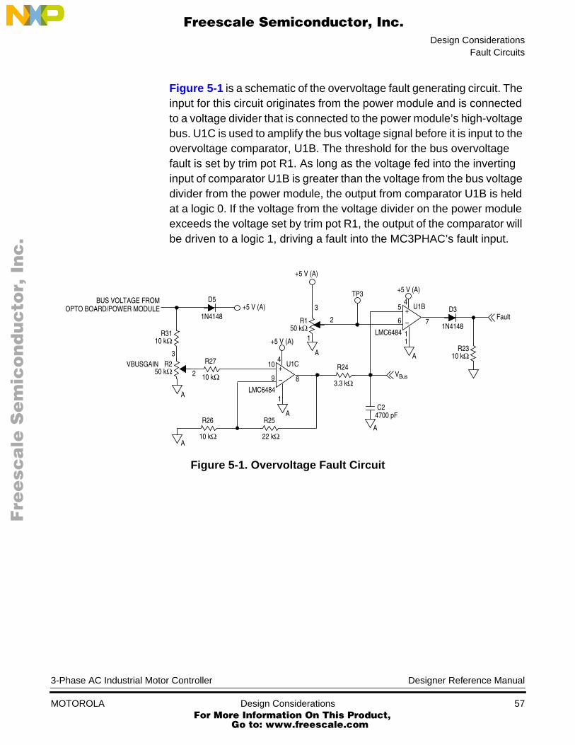
Design ConsiderationsFault Circuits
F
ree
sca
le S
em
ico
nd
uc
tor,
I
Freescale Semiconductor, Inc.n
c..
.
Figure 5-1 is a schematic of the overvoltage fault generating circuit. Theinput for this circuit originates from the power module and is connectedto a voltage divider that is connected to the power module’s high-voltagebus. U1C is used to amplify the bus voltage signal before it is input to theovervoltage comparator, U1B. The threshold for the bus overvoltagefault is set by trim pot R1. As long as the voltage fed into the invertinginput of comparator U1B is greater than the voltage from the bus voltagedivider from the power module, the output from comparator U1B is heldat a logic 0. If the voltage from the voltage divider on the power moduleexceeds the voltage set by trim pot R1, the output of the comparator willbe driven to a logic 1, driving a fault into the MC3PHAC’s fault input.
Figure 5-1. Overvoltage Fault Circuit
BUS VOLTAGE FROM
LMC6484
+5 V (A)
1
+
–9
103
A
U1C
8
R27
10 kΩ
R26
10 kΩA
R25
22 kΩ
R250 kΩ
A
R3110 kΩ
D5
1N4148+5 V (A)OPTO BOARD/POWER MODULE
4
2R24
3.3 kΩ
4700 pFC2
A
VBus
LMC6484
+5 V (A)
1
+
–6
5
A
U1B4
1
TP3
2R150 kΩ
+5 V (A)
1
A
3 D3
1N41487
R2310 kΩ
Fault
VBUSGAIN
3-Phase AC Industrial Motor Controller Designer Reference Manual
MOTOROLA Design Considerations 57 For More Information On This Product,
Go to: www.freescale.com
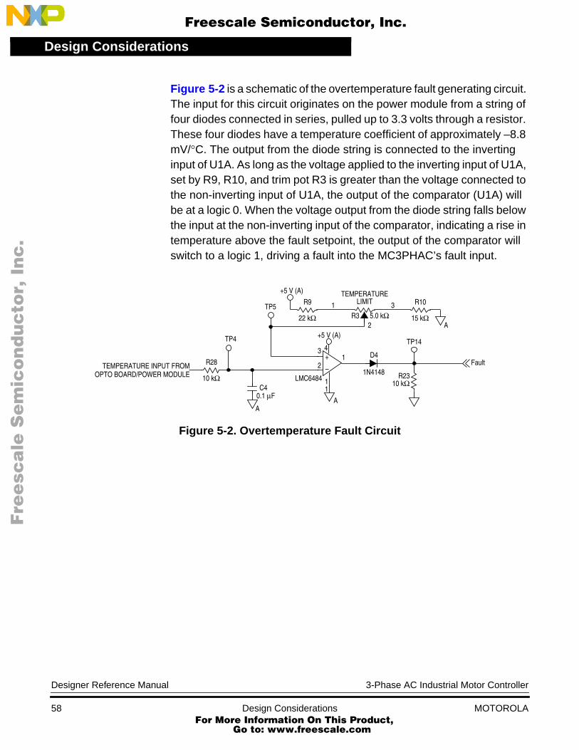
Design Considerations
F
ree
sca
le S
em
ico
nd
uc
tor,
I
Freescale Semiconductor, Inc.n
c..
.
Figure 5-2 is a schematic of the overtemperature fault generating circuit.The input for this circuit originates on the power module from a string offour diodes connected in series, pulled up to 3.3 volts through a resistor.These four diodes have a temperature coefficient of approximately –8.8mV/°C. The output from the diode string is connected to the invertinginput of U1A. As long as the voltage applied to the inverting input of U1A,set by R9, R10, and trim pot R3 is greater than the voltage connected tothe non-inverting input of U1A, the output of the comparator (U1A) willbe at a logic 0. When the voltage output from the diode string falls belowthe input at the non-inverting input of the comparator, indicating a rise intemperature above the fault setpoint, the output of the comparator willswitch to a logic 1, driving a fault into the MC3PHAC’s fault input.
Figure 5-2. Overtemperature Fault Circuit
0.1 µFC4
Fault
R2310 kΩ
+
–
D4
LMC6484
TP14
A
R28
10 kΩ
AA
+5 V (A)TP4
TP5
+5 V (A)
R9
22 kΩ
R10
15 kΩR3 5.0 kΩ
TEMPERATURELIMIT
11
2
3 41
1 3
2
TEMPERATURE INPUT FROMOPTO BOARD/POWER MODULE 1N4148
Designer Reference Manual 3-Phase AC Industrial Motor Controller
58 Design Considerations MOTOROLA For More Information On This Product,
Go to: www.freescale.com
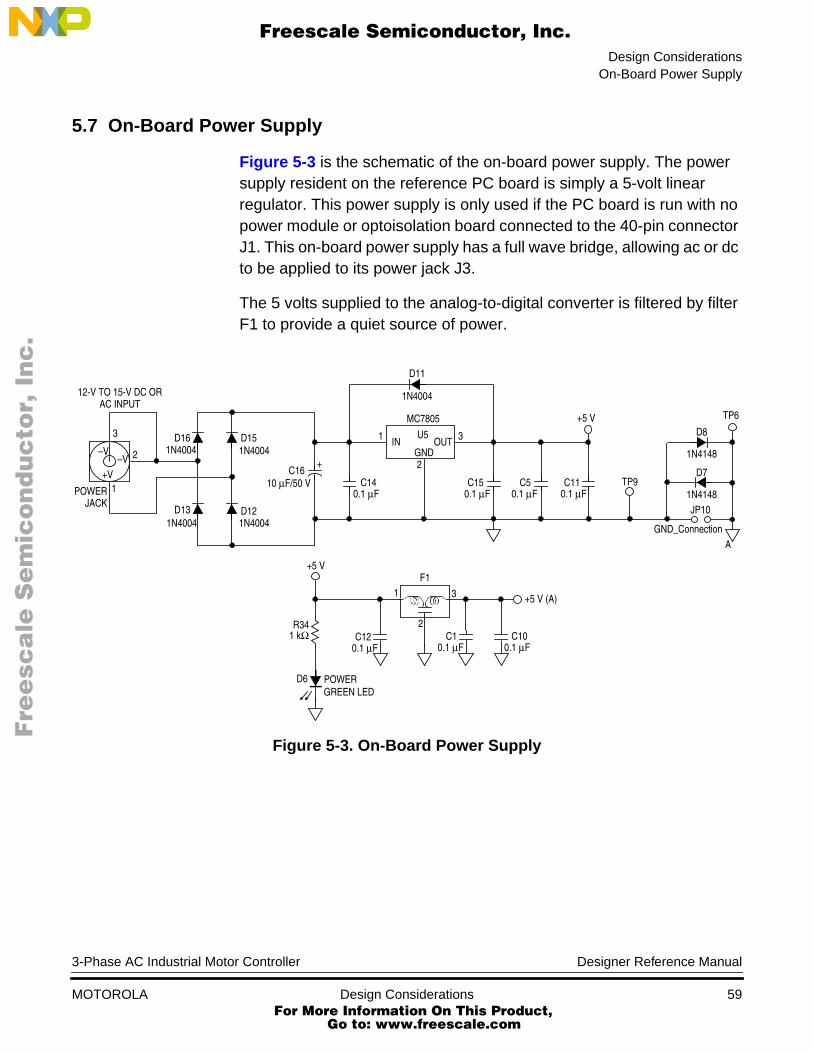
Design ConsiderationsOn-Board Power Supply
F
ree
sca
le S
em
ico
nd
uc
tor,
I
Freescale Semiconductor, Inc.n
c..
.
5.7 On-Board Power Supply
Figure 5-3 is the schematic of the on-board power supply. The powersupply resident on the reference PC board is simply a 5-volt linearregulator. This power supply is only used if the PC board is run with nopower module or optoisolation board connected to the 40-pin connectorJ1. This on-board power supply has a full wave bridge, allowing ac or dcto be applied to its power jack J3.
The 5 volts supplied to the analog-to-digital converter is filtered by filterF1 to provide a quiet source of power.
Figure 5-3. On-Board Power Supply
–V–V
+V1
2
3
12-V TO 15-V DC OR
POWERJACK
AC INPUT
D16
1N4004
1N4004
D13
D15
D121N4004
1N4004
C1610 µF/50 V
+
C140.1 µF
1
2
3IN OUTGND
U5
MC7805
D11
1N4004
0.1 µFC15
0.1 µFC5
0.1 µFC11 TP9
+5 V
A
JP10
GND_Connection
TP6
D8
1N4148
D7
1N4148
F1+5 V
R341 kΩ
D6 POWERGREEN LED
0.1 µFC12
2
1 3
0.1 µFC1 C10
0.1 µF
+5 V (A)
3-Phase AC Industrial Motor Controller Designer Reference Manual
MOTOROLA Design Considerations 59 For More Information On This Product,
Go to: www.freescale.com
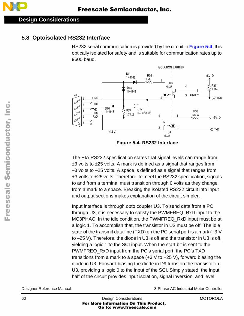
Design Considerations
F
ree
sca
le S
em
ico
nd
uc
tor,
I
Freescale Semiconductor, Inc.n
c..
.
5.8 Optoisolated RS232 Interface
RS232 serial communication is provided by the circuit in Figure 5-4. It isoptically isolated for safety and is suitable for communication rates up to9600 baud.
Figure 5-4. RS232 Interface
The EIA RS232 specification states that signal levels can range from±3 volts to ±25 volts. A mark is defined as a signal that ranges from–3 volts to –25 volts. A space is defined as a signal that ranges from+3 volts to +25 volts. Therefore, to meet the RS232 specification, signalsto and from a terminal must transition through 0 volts as they changefrom a mark to a space. Breaking the isolated RS232 circuit into inputand output sections makes explanation of the circuit simpler.
Input interface is through opto coupler U3. To send data from a PCthrough U3, it is necessary to satisfy the PWMFREQ_RxD input to theMC3PHAC. In the idle condition, the PWMFREQ_RxD input must be ata logic 1. To accomplish that, the transistor in U3 must be off. The idlestate of the transmit data line (TXD) on the PC serial port is a mark (–3 Vto –25 V). Therefore, the diode in U3 is off and the transistor in U3 is off,yielding a logic 1 to the SCI input. When the start bit is sent to thePWMFREQ_RxD input from the PC’s serial port, the PC’s TXDtransitions from a mark to a space (+3 V to +25 V), forward biasing thediode in U3. Forward biasing the diode in D9 turns on the transistor inU3, providing a logic 0 to the input of the SCI. Simply stated, the inputhalf of the circuit provides input isolation, signal inversion, and level
59
48
37
26
1
J2GND
DTR
TxDRTSRxD
(+12 V)
D101N4148 R39
4.7 kΩC172.2 µF/50V
+
D141N4148
D91N4148
R361 kΩ
U34N35
R38
4N35
330 Ω+5V_D
TxD
RxD
1
2
4
3
1
2
4
3
U4
GND
+5V_D
R371 kΩ
ISOLATION BARRIER
Designer Reference Manual 3-Phase AC Industrial Motor Controller
60 Design Considerations MOTOROLA For More Information On This Product,
Go to: www.freescale.com
Design ConsiderationsOptoisolated RS232 Interface
F
ree
sca
le S
em
ico
nd
uc
tor,
I
Freescale Semiconductor, Inc.n
c..
.
shifting from the PC to the MC3PHAC’s PWMFREQ_RxD pin. An RS232line receiver, such as an MC1489, serves the same purpose without theoptoisolation function.
To send data from the M3PHAC’s RETRY_TxD pin to a PC serial portinput, it is necessary to satisfy the PC’s receive data (RXD) inputrequirements. In an idle condition, the RXD input to the PC must be atmark (–3 V to –25 V). The data terminal ready output (DTR) on the PCoutputs a mark when the port is initialized. The request to send RTSoutput is set to a space (+3 V to +25 V) when the PC’s serial port isinitialized. Because the interface is half-duplex, the PC’s TXD output isalso at a mark, as it is idle. The idle state of the transmit data line(RETRY_TxD) on the MC3PHAC’s serial port is a logic 1. The logic 1 outof the serial port output port forces the diode in U4 to be turned off. Withthe diode in U4 turned off, the transistor in U4 is also turned off. Thejunction of D10 and D14 are at a mark (–3 V to –25 V). With the transistorin U4 turned off, the input is pulled to a mark through current limitingresistor R39, satisfying the PC’s serial input in an idle condition. When astart bit is sent from the MC3PHAC’s serial port, the output of theMC3PHAC’s serial port transitions to a logic 0. That logic 0 turns on thediode in U5, thus turning on the transistor in U5. The conductingtransistor in U5 passes the voltage output from the PC’s RTS output, thatis now at a space (+3 V to +25 V) to the PC’s receive data (RXD) input.Capacitor C17 is a bypass capacitor used to “stiffen” the mark signal.The output half of the circuit provides output isolation, signal inversion,and level shifting from the MC3PHAC’s serial output port to the PC’sserial port. An RS232 line driver, such as an MC1488, serves the samepurpose without the optoisolation function.
3-Phase AC Industrial Motor Controller Designer Reference Manual
MOTOROLA Design Considerations 61 For More Information On This Product,
Go to: www.freescale.com

Design Considerations
F
ree
sca
le S
em
ico
nd
uc
tor,
I
Freescale Semiconductor, Inc.n
c..
.
Designer Reference Manual 3-Phase AC Industrial Motor Controller
62 Design Considerations MOTOROLA For More Information On This Product,
Go to: www.freescale.com

F
ree
sca
le S
em
ico
nd
uc
tor,
I
Freescale Semiconductor, Inc.n
c..
.
Appendix A. MC3PHAC Data Sheet
For More Information On This Product,
Go to: www.freescale.com

F
ree
sca
le S
em
ico
nd
uc
tor,
I
Freescale Semiconductor, Inc.n
c..
.
For More Information On This Product,
Go to: www.freescale.com

MC3PHAC/DRev. 1, 4/2002
3-Phase AC MotorController
Data Sheet
F
ree
sca
le S
em
ico
nd
uc
tor,
I
Freescale Semiconductor, Inc.n
c..
.
Overview
The MC3PHAC is a high-performance monolithic intelligent motor controllerdesigned specifically to meet the requirements for low-cost, variable-speed,3-phase ac motor control systems. The device is adaptable and configurable,based on its environment. It contains all of the active functions required toimplement the control portion of an open loop, 3-phase ac motor drive.
One of the unique aspects of this device is that although it is adaptable andconfigurable based on its environment, it does not require any softwaredevelopment. This makes the MC3PHAC a perfect fit for customer applicationsrequiring ac motor control but with limited or no software resources available.
The device features are:
• Volts-per-Hertz speed control
• Digital signal processing (DSP) filtering to enhance speed stability
• 32-bit calculations for high-precision operation
• Internet enabled
• No user software development required for operation
• 6-output pulse-width modulator (PWM)
• 3-phase waveform generation
• 4-channel analog-to-digital converter (ADC)
• User configurable for standalone or hosted operation
• Dynamic bus ripple cancellation
• Selectable PWM polarity and frequency
• Selectable 50/60 Hz base frequency
• Phase-lock loop (PLL) based system oscillator
• Serial communications interface (SCI)
• Low-power supply voltage detection circuit
© Motorola, Inc., 2002
For More Information On This Product, Go to: www.freescale.com

MC3PHAC/D
F
ree
sca
le S
em
ico
nd
uc
tor,
I
Freescale Semiconductor, Inc.n
c..
.
Included in the MC3PHAC are protective features consisting of dc bus voltagemonitoring and a system fault input that will immediately disable the PWMmodule upon detection of a system fault.
Some target applications for the MC3PHAC include:
• Low horsepower HVAC motors
• Home appliances
• Commercial laundry and dishwashers
• Process control
• Pumps and fans
As shown in Table 1, the MC3PHAC is offered in these packages:
• Plastic 28-pin dual in-line package (DIP)
• Plastic 28-pin small outline integrated circuit (SOIC)
• Plastic 32-pin quad flat pack (QFP)
See Figure 1 and Figure 2 for the pin connections.
Table 1. Ordering Information
DeviceOperating
Temperature RangePackage
MC3PHACVP –40°C to +105°C Plastic 28-pin DIP
MC3PHACVDW –40°C to +105°C Plastic 28-pin SOIC
MC3PHACVFA –40°C to +105°C Plastic 32-pin QFP
66 3-Phase AC Motor Controller MOTOROLA
For More Information On This Product, Go to: www.freescale.com
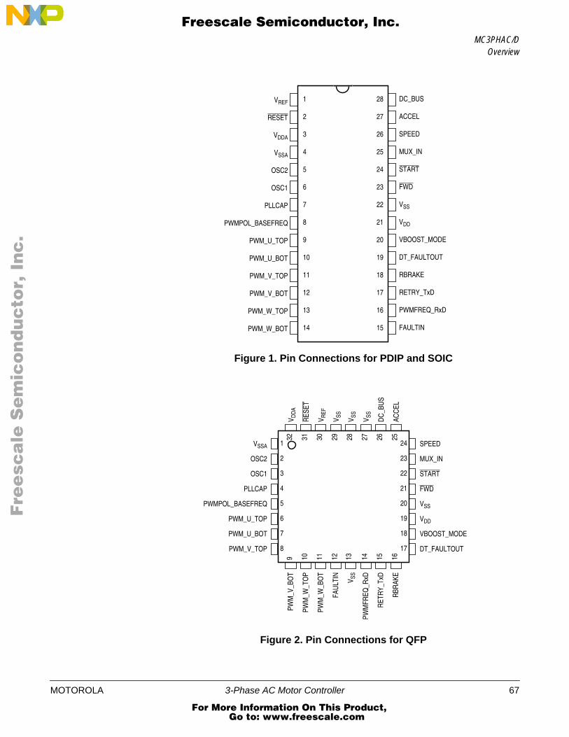
MC3PHAC/DOverview
F
ree
sca
le S
em
ico
nd
uc
tor,
I
Freescale Semiconductor, Inc.n
c..
.
Figure 1. Pin Connections for PDIP and SOIC
Figure 2. Pin Connections for QFP
VREF 1
2
3
4
5
6
7
8
9
10
11
12
13
14
28
27
26
25
24
23
22
21
20
19
18
17
16
15
RESET
VDDA
VSSA
OSC2
OSC1
PLLCAP
PWMPOL_BASEFREQ
PWM_U_TOP
PWM_U_BOT
PWM_V_TOP
PWM_V_BOT
PWM_W_TOP
PWM_W_BOT FAULTIN
PWMFREQ_RxD
RETRY_TxD
RBRAKE
DT_FAULTOUT
VBOOST_MODE
VDD
VSS
FWD
START
MUX_IN
SPEED
ACCEL
DC_BUS
PWM
_V_B
OT
PWM
_W_T
OP
PWM
_W_B
OT
FAU
LTIN
V SS
PWM
FREQ
_RxD
RET
RY_
TxD
RBR
AKE
9 10 11 12 13 14 15 16
PWM_V_TOP
START
PWM_U_BOT
PWM_U_TOP
PWMPOL_BASEFREQ
PLLCAP
OSC1
OSC2
VSSA SPEED
MUX_IN
FWD
VSS
VDD
VBOOST_MODE
DT_FAULTOUT
2
3
4
5
6
7
8
24
23
22
21
20
19
18
17
32 31 30 29 28 27 26 25
1
V REF
V DD
A
RES
ET
V SS
V SS
V SS
DC
_BU
S
ACC
EL
MOTOROLA 3-Phase AC Motor Controller 67
For More Information On This Product, Go to: www.freescale.com
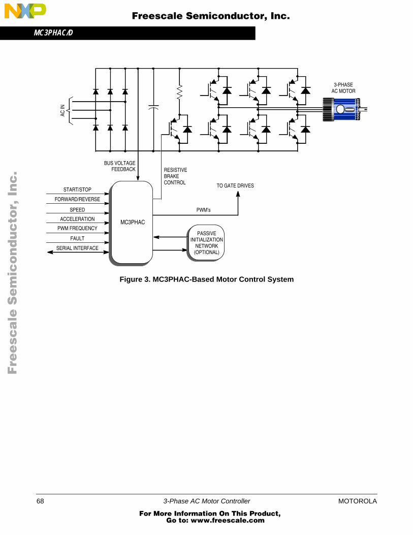
MC3PHAC/D
F
ree
sca
le S
em
ico
nd
uc
tor,
I
Freescale Semiconductor, Inc.n
c..
.
Figure 3. MC3PHAC-Based Motor Control System
3-PHASEAC MOTOR
AC IN
BUS VOLTAGEFEEDBACK RESISTIVE
BRAKECONTROL
PWM’s
START/STOP
FORWARD/REVERSE
SPEED
ACCELERATION
PWM FREQUENCYMC3PHAC
FAULT
SERIAL INTERFACE
PASSIVEINITIALIZATION
NETWORK(OPTIONAL)
TO GATE DRIVES
68 3-Phase AC Motor Controller MOTOROLA
For More Information On This Product, Go to: www.freescale.com
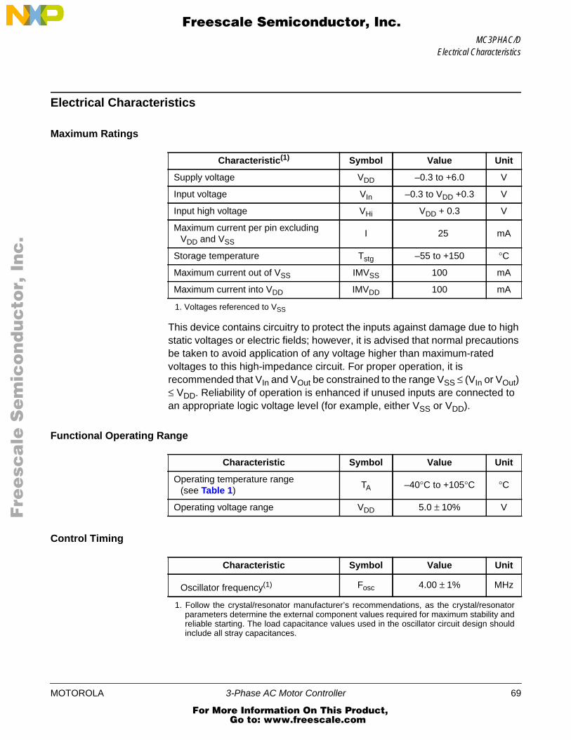
MC3PHAC/DElectrical Characteristics
F
ree
sca
le S
em
ico
nd
uc
tor,
I
Freescale Semiconductor, Inc.n
c..
.
Electrical Characteristics
Maximum Ratings
This device contains circuitry to protect the inputs against damage due to highstatic voltages or electric fields; however, it is advised that normal precautionsbe taken to avoid application of any voltage higher than maximum-ratedvoltages to this high-impedance circuit. For proper operation, it isrecommended that VIn and VOut be constrained to the range VSS ≤ (VIn or VOut)≤ VDD. Reliability of operation is enhanced if unused inputs are connected toan appropriate logic voltage level (for example, either VSS or VDD).
Functional Operating Range
Control Timing
Characteristic(1)
1. Voltages referenced to VSS
Symbol Value Unit
Supply voltage VDD –0.3 to +6.0 V
Input voltage VIn –0.3 to VDD +0.3 V
Input high voltage VHi VDD + 0.3 V
Maximum current per pin excludingVDD and VSS
I 25 mA
Storage temperature Tstg –55 to +150 °C
Maximum current out of VSS IMVSS 100 mA
Maximum current into VDD IMVDD 100 mA
Characteristic Symbol Value Unit
Operating temperature range(see Table 1)
TA –40°C to +105°C °C
Operating voltage range VDD 5.0 ± 10% V
Characteristic Symbol Value Unit
Oscillator frequency(1)
1. Follow the crystal/resonator manufacturer’s recommendations, as the crystal/resonatorparameters determine the external component values required for maximum stability andreliable starting. The load capacitance values used in the oscillator circuit design shouldinclude all stray capacitances.
Fosc 4.00 ± 1% MHz
MOTOROLA 3-Phase AC Motor Controller 69
For More Information On This Product, Go to: www.freescale.com
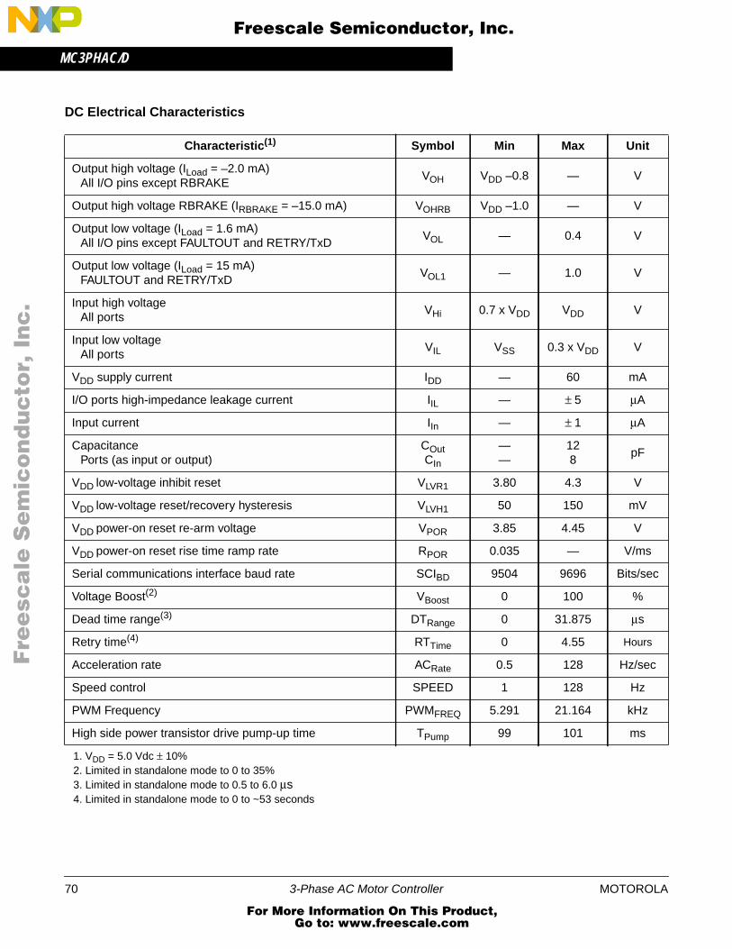
MC3PHAC/D
F
ree
sca
le S
em
ico
nd
uc
tor,
I
Freescale Semiconductor, Inc.n
c..
.
DC Electrical Characteristics
Characteristic(1) Symbol Min Max Unit
Output high voltage (ILoad = –2.0 mA)All I/O pins except RBRAKE
VOH VDD –0.8 — V
Output high voltage RBRAKE (IRBRAKE = –15.0 mA) VOHRB VDD –1.0 — V
Output low voltage (ILoad = 1.6 mA)All I/O pins except FAULTOUT and RETRY/TxD
VOL — 0.4 V
Output low voltage (ILoad = 15 mA)FAULTOUT and RETRY/TxD
VOL1 — 1.0 V
Input high voltageAll ports
VHi 0.7 x VDD VDD V
Input low voltageAll ports
VIL VSS 0.3 x VDD V
VDD supply current IDD — 60 mA
I/O ports high-impedance leakage current IIL — ± 5 µA
Input current IIn — ± 1 µA
CapacitancePorts (as input or output)
COutCIn
——
128
pF
VDD low-voltage inhibit reset VLVR1 3.80 4.3 V
VDD low-voltage reset/recovery hysteresis VLVH1 50 150 mV
VDD power-on reset re-arm voltage VPOR 3.85 4.45 V
VDD power-on reset rise time ramp rate RPOR 0.035 — V/ms
Serial communications interface baud rate SCIBD 9504 9696 Bits/sec
Voltage Boost(2) VBoost 0 100 %
Dead time range(3) DTRange 0 31.875 µs
Retry time(4) RTTime 0 4.55 Hours
Acceleration rate ACRate 0.5 128 Hz/sec
Speed control SPEED 1 128 Hz
PWM Frequency PWMFREQ 5.291 21.164 kHz
High side power transistor drive pump-up time TPump 99 101 ms
1. VDD = 5.0 Vdc ± 10%2. Limited in standalone mode to 0 to 35%3. Limited in standalone mode to 0.5 to 6.0 µs4. Limited in standalone mode to 0 to ~53 seconds
70 3-Phase AC Motor Controller MOTOROLA
For More Information On This Product, Go to: www.freescale.com
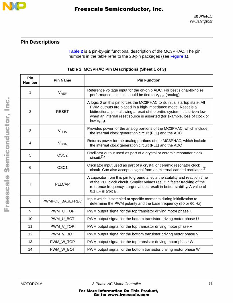
MC3PHAC/DPin Descriptions
F
ree
sca
le S
em
ico
nd
uc
tor,
I
Freescale Semiconductor, Inc.n
c..
.
Pin Descriptions
Table 2 is a pin-by-pin functional description of the MC3PHAC. The pinnumbers in the table refer to the 28-pin packages (see Figure 1).
Table 2. MC3PHAC Pin Descriptions (Sheet 1 of 3)
PinNumber
Pin Name Pin Function
1 VREFReference voltage input for the on-chip ADC. For best signal-to-noise
performance, this pin should be tied to VDDA (analog).
2 RESET
A logic 0 on this pin forces the MC3PHAC to its initial startup state. AllPWM outputs are placed in a high-impedance mode. Reset is abidirectional pin, allowing a reset of the entire system. It is driven lowwhen an internal reset source is asserted (for example, loss of clock orlow VDD).
3 VDDAProvides power for the analog portions of the MC3PHAC, which include
the internal clock generation circuit (PLL) and the ADC
4 VSSAReturns power for the analog portions of the MC3PHAC, which include
the internal clock generation circuit (PLL) and the ADC
5 OSC2Oscillator output used as part of a crystal or ceramic resonator clock
circuit.(1)
6 OSC1Oscillator input used as part of a crystal or ceramic resonator clock
circuit. Can also accept a signal from an external canned oscillator.(1)
7 PLLCAP
A capacitor from this pin to ground affects the stability and reaction timeof the PLL clock circuit. Smaller values result in faster tracking of thereference frequency. Larger values result in better stability. A value of0.1 µF is typical.
8 PWMPOL_BASEFREQInput which is sampled at specific moments during initialization to
determine the PWM polarity and the base frequency (50 or 60 Hz)
9 PWM_U_TOP PWM output signal for the top transistor driving motor phase U
10 PWM_U_BOT PWM output signal for the bottom transistor driving motor phase U
11 PWM_V_TOP PWM output signal for the top transistor driving motor phase V
12 PWM_V_BOT PWM output signal for the bottom transistor driving motor phase V
13 PWM_W_TOP PWM output signal for the top transistor driving motor phase W
14 PWM_W_BOT PWM output signal for the bottom transistor driving motor phase W
MOTOROLA 3-Phase AC Motor Controller 71
For More Information On This Product, Go to: www.freescale.com
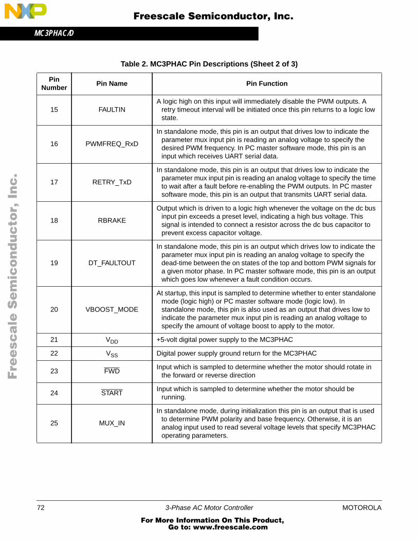
MC3PHAC/D
F
ree
sca
le S
em
ico
nd
uc
tor,
I
Freescale Semiconductor, Inc.n
c..
.
15 FAULTINA logic high on this input will immediately disable the PWM outputs. A
retry timeout interval will be initiated once this pin returns to a logic lowstate.
16 PWMFREQ_RxD
In standalone mode, this pin is an output that drives low to indicate theparameter mux input pin is reading an analog voltage to specify thedesired PWM frequency. In PC master software mode, this pin is aninput which receives UART serial data.
17 RETRY_TxD
In standalone mode, this pin is an output that drives low to indicate theparameter mux input pin is reading an analog voltage to specify the timeto wait after a fault before re-enabling the PWM outputs. In PC mastersoftware mode, this pin is an output that transmits UART serial data.
18 RBRAKE
Output which is driven to a logic high whenever the voltage on the dc businput pin exceeds a preset level, indicating a high bus voltage. Thissignal is intended to connect a resistor across the dc bus capacitor toprevent excess capacitor voltage.
19 DT_FAULTOUT
In standalone mode, this pin is an output which drives low to indicate theparameter mux input pin is reading an analog voltage to specify thedead-time between the on states of the top and bottom PWM signals fora given motor phase. In PC master software mode, this pin is an outputwhich goes low whenever a fault condition occurs.
20 VBOOST_MODE
At startup, this input is sampled to determine whether to enter standalonemode (logic high) or PC master software mode (logic low). Instandalone mode, this pin is also used as an output that drives low toindicate the parameter mux input pin is reading an analog voltage tospecify the amount of voltage boost to apply to the motor.
21 VDD +5-volt digital power supply to the MC3PHAC
22 VSS Digital power supply ground return for the MC3PHAC
23 FWDInput which is sampled to determine whether the motor should rotate in
the forward or reverse direction
24 STARTInput which is sampled to determine whether the motor should be
running.
25 MUX_IN
In standalone mode, during initialization this pin is an output that is usedto determine PWM polarity and base frequency. Otherwise, it is ananalog input used to read several voltage levels that specify MC3PHACoperating parameters.
Table 2. MC3PHAC Pin Descriptions (Sheet 2 of 3)
PinNumber
Pin Name Pin Function
72 3-Phase AC Motor Controller MOTOROLA
For More Information On This Product, Go to: www.freescale.com
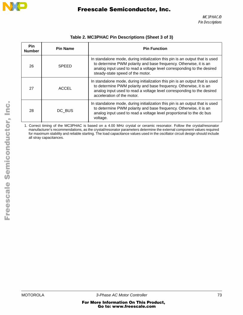
MC3PHAC/DPin Descriptions
F
ree
sca
le S
em
ico
nd
uc
tor,
I
Freescale Semiconductor, Inc.n
c..
.
26 SPEED
In standalone mode, during initialization this pin is an output that is usedto determine PWM polarity and base frequency. Otherwise, it is ananalog input used to read a voltage level corresponding to the desiredsteady-state speed of the motor.
27 ACCEL
In standalone mode, during initialization this pin is an output that is usedto determine PWM polarity and base frequency. Otherwise, it is ananalog input used to read a voltage level corresponding to the desiredacceleration of the motor.
28 DC_BUS
In standalone mode, during initialization this pin is an output that is usedto determine PWM polarity and base frequency. Otherwise, it is ananalog input used to read a voltage level proportional to the dc busvoltage.
1. Correct timing of the MC3PHAC is based on a 4.00 MHz crystal or ceramic resonator. Follow the crystal/resonatormanufacturer’s recommendations, as the crystal/resonator parameters determine the external component values requiredfor maximum stability and reliable starting. The load capacitance values used in the oscillator circuit design should includeall stray capacitances.
Table 2. MC3PHAC Pin Descriptions (Sheet 3 of 3)
PinNumber
Pin Name Pin Function
MOTOROLA 3-Phase AC Motor Controller 73
For More Information On This Product, Go to: www.freescale.com
MC3PHAC/D
F
ree
sca
le S
em
ico
nd
uc
tor,
I
Freescale Semiconductor, Inc.n
c..
.
Introduction
The MC3PHAC is a high-performance intelligent controller designedspecifically to meet the requirements for low-cost, variable-speed,3-phase ac motor control systems. The device is adaptable and configurable,based on its environment. Constructed with high-speed CMOS(complementary metal-oxide semiconductor) technology, the MC3PHAC offersa high degree of performance and ruggedness in the hostile environmentsoften found in motor control systems.
The device consists of:
• 6-output pulse-width modulator (PWM)
• 4-channel analog-to-digital converter (ADC)
• Phase-lock loop (PLL) based system oscillator
• Low-power supply voltage detection circuit
• Serial communications interface (SCI)
The serial communications interface is used in a mode, called PC mastersoftware mode, whereby control of the MC3PHAC is from a host or masterpersonal computer executing PC master software or a microcontrolleremulating PC master software commands. In either case, control via theinternet is feasible.
Included in the MC3PHAC are protective features consisting of dc busmonitoring and a system fault input that will immediately disable the PWMmodule upon detection of a system fault.
Included motor control features include:
• Open loop volts/Hertz speed control
• Forward or reverse rotation
• Start/stop motion
• System fault input
• Low-speed voltage boost
• Internal power-on reset (POR)
74 3-Phase AC Motor Controller MOTOROLA
For More Information On This Product, Go to: www.freescale.com
MC3PHAC/DFeatures
F
ree
sca
le S
em
ico
nd
uc
tor,
I
Freescale Semiconductor, Inc.n
c..
.
Features
3-Phase Waveform Generation — The MC3PHAC generates six PWMsignals which have been modulated with variable voltage and variablefrequency information in order to control a 3-phase ac motor. A third harmonicsignal has been superimposed on top of the fundamental motor frequency toachieve full bus voltage utilization. This results in a 15 percent increase inmaximum output amplitude compared to pure sine wave modulation.
The waveform is updated at a 5.3 kHz rate (except when the PWM frequencyis 15.9 kHz), resulting in near continuous waveform quality. At 15.9 kHz, thewaveform is updated at 4.0 kHz.
DSP Filtering — A 24-bit IIR digital filter is used on the SPEED input signal instandalone mode, resulting in enhanced speed stability in noisy environments.The sampling period of the filter is 3 ms (except when the PWM frequency is15.9 kHz) and it mimics the response of a single pole analog filter having a poleat 0.4 Hz. At a PWM frequency of 15.9 kHz, the sampling period is 4 ms andthe pole is located at 0.3 Hz.
High Precision Calculations — Up to 32-bit variable resolution is employedfor precision control and smooth performance. For example, the motor speedcan be controlled with a resolution of 4 mHz.
Smooth Voltage Transitions — When the commanded speed of the motorpasses through ±1 Hz, the voltage is gently applied or removed depending onthe direction of the speed change. This eliminates any pops or surges that mayoccur, especially under conditions of high-voltage boost at low frequencies.
High-Side Bootstrapping — Many motor drive topologies (especially high-voltage drives) use optocouplers to supply the PWM signal to the high-sidetransistors. Often, the high-side transistor drive circuitry contains a chargepump circuit to create a floating power supply for each high-side transistor thatis dependent on low-side PWMs to develop power. When the motor has beenoff for a period of time, the charge on the high-side power supply capacitor isdepleted and must be replenished before proper PWM operation can resume.
To accommodate such topologies, the MC3PHAC will always provide 100 msof 50 percent PWM drive to only the low-side transistors each time the motor isturned on. Since the top transistors remain off during this time, it has the effectof applying zero volts to the motor, and no motion occurs. After this period,motor waveform modulation begins, with PWM drive also being applied to thehigh-side transistors.
Fast Velocity Updating — During periods when the motor speed is changing,the rate at which the velocity is updated is critical to smooth operation. If theseupdates occur too infrequently, a ratcheting effect will be exhibited on themotor, which inhibits smooth torque performance. However, velocity profiling is
MOTOROLA 3-Phase AC Motor Controller 75
For More Information On This Product, Go to: www.freescale.com
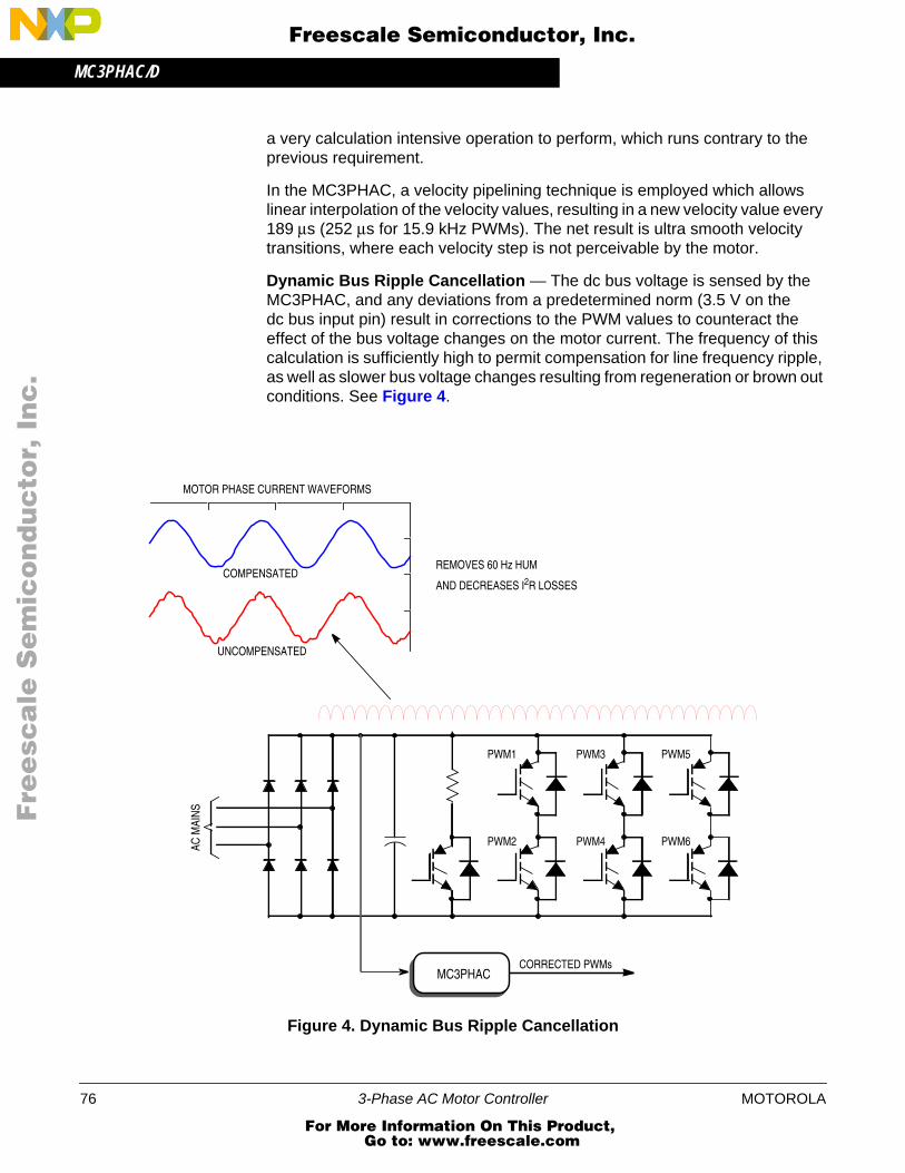
MC3PHAC/D
F
ree
sca
le S
em
ico
nd
uc
tor,
I
Freescale Semiconductor, Inc.n
c..
.
a very calculation intensive operation to perform, which runs contrary to theprevious requirement.
In the MC3PHAC, a velocity pipelining technique is employed which allowslinear interpolation of the velocity values, resulting in a new velocity value every189 µs (252 µs for 15.9 kHz PWMs). The net result is ultra smooth velocitytransitions, where each velocity step is not perceivable by the motor.
Dynamic Bus Ripple Cancellation — The dc bus voltage is sensed by theMC3PHAC, and any deviations from a predetermined norm (3.5 V on thedc bus input pin) result in corrections to the PWM values to counteract theeffect of the bus voltage changes on the motor current. The frequency of thiscalculation is sufficiently high to permit compensation for line frequency ripple,as well as slower bus voltage changes resulting from regeneration or brown outconditions. See Figure 4.
Figure 4. Dynamic Bus Ripple Cancellation
AC M
AIN
S
PWM1
PWM2
PWM3
PWM4
PWM5
PWM6
MC3PHACCORRECTED PWMs
MOTOR PHASE CURRENT WAVEFORMS
UNCOMPENSATED
COMPENSATEDREMOVES 60 Hz HUM
AND DECREASES I2R LOSSES
76 3-Phase AC Motor Controller MOTOROLA
For More Information On This Product, Go to: www.freescale.com
MC3PHAC/DFeatures
F
ree
sca
le S
em
ico
nd
uc
tor,
I
Freescale Semiconductor, Inc.n
c..
.
Selectable Base Frequency — Alternating current (ac) motors are designedto accept rated voltage at either 50 or 60 Hz, depending on what region of theworld they were designed to be used. The MC3PHAC can accommodate bothtypes of motors by allowing the voltage profile to reach maximum value ateither 50 or 60 Hz. This parameter can be specified at initialization instandalone mode, or it can be changed at any time in PC master softwaremode.
Selectable PWM Polarity — The polarity of the PWM outputs may bespecified such that a logic high on a PWM output can either be the asserted ornegated state of the signal. In standalone mode, this parameter is specified atinitialization and applies to all six PWM outputs. In PC master software mode,the polarity of the top PWM signals can be specified separately from thepolarity of the bottom PWM signals.
This specification can be done at any time, but once it is done, the polaritiesare locked and cannot be changed until a reset occurs. Also, any commandsfrom PC master software that would have the effect of enabling PWMs areprevented by the MC3PHAC until the polarity has been specified.
In standalone mode, the base frequency and PWM polarity are specified at thesame time during initialization by connecting either pin 25, 26, 27, or 28exclusively to the PWMPOL_BASEFREQ input. During initialization, pins 25,26, 27, and 28 are cycled one at a time to determine which one has beenconnected to the PWMPOL_BASEFREQ input.
Table 3 shows the selected PWM polarity and base frequency as a function ofwhich pin connection is made. Refer to the standalone mode schematic,Figure 8. Only one of these jumpers (JP1–JP4) can be connected at any onetime.
NOTE: It is not necessary to break this connection once the initialization phase hasbeen completed. The MC3PHAC will function properly while this connection isin place.
Table 3. PWM Polarity and Base FrequencySpecification in Standalone Mode
Pin Connected toPWMPOL_BASEFREQ Pin
PWM PolarityBase
Frequency
MUX_IN (JP1) Logic low = on 50 Hz
SPEED (JP2) Logic high = on 50 Hz
ACCEL (JP3) Logic low = on 60 Hz
DC_BUS (JP4) Logic high = on 60 Hz
MOTOROLA 3-Phase AC Motor Controller 77
For More Information On This Product, Go to: www.freescale.com

MC3PHAC/D
F
ree
sca
le S
em
ico
nd
uc
tor,
I
Freescale Semiconductor, Inc.n
c..
.
Selectable PWM Frequency — The MC3PHAC accommodates four discretePWM frequencies and can be changed dynamically while the motor is running.This resistor can be a potentiometer or a fixed resistor in the range shown inTable 4. In standalone mode, the PWM frequency is specified by applying avoltage to the MUX_IN pin while the PWMFREQ_RxD pin is being driven low.Table 4 shows the required voltage levels on the MUX_IN pin and theassociated PWM frequency for each voltage range.
NOTE: The PWM frequencies are based on a 4.00 MHz frequency applied to theoscillator input.
Selectable PWM Dead Time — Besides being able to specify the PWMfrequency, the blanking time interval between the on states of thecomplementary PWM pairs can also be specified. Refer to the graph inFigure 9 for the resistance value versus dead time. Figure 9 assumes a6.8 kΩ ±5% pullup resistor. In standalone mode, this is done by
supplying a voltage to the MUX_IN pin while the DT_FAULTOUT pin is beingdriven low. In this way, dead time can be specified with a scaling factor of2.075 µs per volt, with a minimum value of 0.5 µs. In PC master software mode,this value can be selected to be anywhere between 0 and 32 µs.
In both standalone and PC master software modes, the dead time value canbe written only once. Further updates of this parameter are locked out until areset condition occurs.
Speed Control — The synchronous motor frequency can be specified in realtime to be any value from 1 Hz to 128 Hz by the voltage applied to the SPEEDpin. The scaling factor is 25.6 Hz per volt. This parameter can also becontrolled directly from PC master software in real time.
The SPEED pin is processed by a 24-bit digital filter to enhance the speedstability in noisy environments. This filter is only activated in standalone mode.
Acceleration Control — Motor acceleration can be specified in real time to bein the range from 0.5 Hz/second, ranging to 128 Hz/second, by the voltageapplied to the ACCEL pin. The scaling factor is 25.6 Hz/second per volt. Thisparameter can also be controlled directly from PC master software in real time.
Table 4. MUX_IN Resistance Rangesand Corresponding PWM Frequencies
Voltage Input PWM Frequency
0 to 1 V 5.291 kHz
1.5 to 2.25 V 10.582 kHz
2.75 to 3.5 V 15.873 kHz
4 to 5 V 21.164 kHz
78 3-Phase AC Motor Controller MOTOROLA
For More Information On This Product, Go to: www.freescale.com
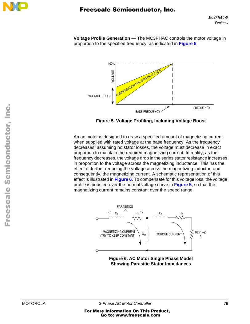
MC3PHAC/DFeatures
F
ree
sca
le S
em
ico
nd
uc
tor,
I
Freescale Semiconductor, Inc.n
c..
.
Voltage Profile Generation — The MC3PHAC controls the motor voltage inproportion to the specified frequency, as indicated in Figure 5.
Figure 5. Voltage Profiling, Including Voltage Boost
An ac motor is designed to draw a specified amount of magnetizing currentwhen supplied with rated voltage at the base frequency. As the frequencydecreases, assuming no stator losses, the voltage must decrease in exactproportion to maintain the required magnetizing current. In reality, as thefrequency decreases, the voltage drop in the series stator resistance increasesin proportion to the voltage across the magnetizing inductance. This has theeffect of further reducing the voltage across the magnetizing inductor, andconsequently, the magnetizing current. A schematic representation of thiseffect is illustrated in Figure 6. To compensate for this voltage loss, the voltageprofile is boosted over the normal voltage curve in Figure 5, so that themagnetizing current remains constant over the speed range.
Figure 6. AC Motor Single Phase ModelShowing Parasitic Stator Impedances
COMPENSATION FOR STATOR LOSSES
VOLT
AGE
FREQUENCYBASE FREQUENCY
VOLTAGE BOOST
100%
PARASITICS
R1 X2 R2
MAGNETIZING CURRENT(TRY TO KEEP CONSTANT) TORQUE CURRENTXM
R2 (1 –s)s
X1
MOTOROLA 3-Phase AC Motor Controller 79
For More Information On This Product, Go to: www.freescale.com

MC3PHAC/D
F
ree
sca
le S
em
ico
nd
uc
tor,
I
Freescale Semiconductor, Inc.n
c..
.
The MC3PHAC allows the voltage boost to be specified as a percentage of fullvoltage at 0 Hz, as shown in Figure 5. In standalone mode, voltage boost isspecified during the initialization phase by supplying a voltage to the MUX_INpin while the VBOOST_MODE pin is being driven low. Refer to the graph inFigure 11 for the resistance value versus voltage boost. Figure 11 assumes a6.8 kΩ pullup resistor. In this way, voltage boost can be specified from 0 to 40percent, with a scaling factor of 8 percent per volt. In PC master softwaremode, the voltage boost can be specified from 0 to 100 percent and can bechanged at anytime.
By using the voltage boost value, and the specified base frequency, theMC3PHAC has all the information required to generate a voltage profileautomatically based on the generated waveform frequency. An additionalfeature exists in PC master software mode whereby this voltage value can beoverridden and controlled in real time. Specifying a voltage lower than thenormal volts-per-hertz profile permits a softer torque response in certainergonomic situations. It also allows for load power factor control and higheroperating efficiencies with high inertia loads or other loads whereinstantaneous changes in torque demand are not permitted. Details of thisfeature are discussed in the PC Master Software Operation with theMC3PHAC.
PLL Clock Generation — The OSC1 pin signal is used as a reference clockfor an internal PLL clocking circuit, which is used to drive the internal clocks ofthe MC3PHAC. This provides excellent protection against noise spikes thatmay occur on the OSC1 pin. In a clocking circuit that does not incorporate aPLL, a noise spike on the clock input can create a clock edge, which violatesthe setup times of the clocking logic, and can cause the device to malfunction.The same noise spike applied to the input of a PLL clock circuit is perceived bythe PLL as a change in its reference frequency, and the PLL output frequencybegins to change in an attempt to lock on to the new frequency. However,before any appreciable change can occur, the spike is gone, and the PLLsettles back into the true reference frequency.
Fault Protection — The MC3PHAC supports an elaborate range of faultprotection and prevention features. If a fault does occur, the MC3PHACimmediately disables the PWMs and waits until the fault condition is clearedbefore starting a timer to re-enable the PWMs. Refer to the graph in Figure 10for the resistance value versus retry time. Figure 10 assumes a 6.8 kΩ pullupresistor. In standalone mode, this timeout interval is specified during theinitialization phase by supplying a voltage to the MUX_IN pin while theRETRY_TxD pin is being driven low. In this way, the retry time can be specifiedfrom 1 to 60 seconds, with a scaling factor of 12 seconds per volt. In PC mastersoftware mode, the retry time can be specified from 0.25 second to over4.5 hours and can be changed at any time.
80 3-Phase AC Motor Controller MOTOROLA
For More Information On This Product, Go to: www.freescale.com
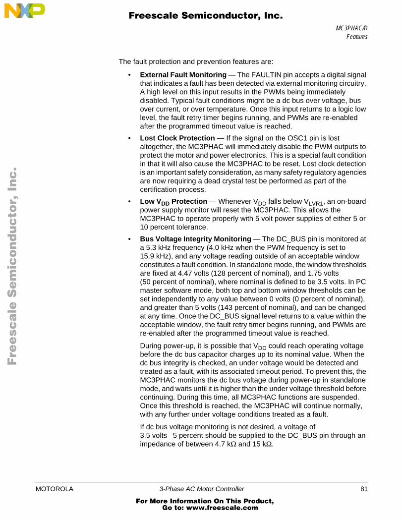
MC3PHAC/DFeatures
F
ree
sca
le S
em
ico
nd
uc
tor,
I
Freescale Semiconductor, Inc.n
c..
.
The fault protection and prevention features are:
• External Fault Monitoring — The FAULTIN pin accepts a digital signalthat indicates a fault has been detected via external monitoring circuitry.A high level on this input results in the PWMs being immediatelydisabled. Typical fault conditions might be a dc bus over voltage, busover current, or over temperature. Once this input returns to a logic lowlevel, the fault retry timer begins running, and PWMs are re-enabledafter the programmed timeout value is reached.
• Lost Clock Protection — If the signal on the OSC1 pin is lostaltogether, the MC3PHAC will immediately disable the PWM outputs toprotect the motor and power electronics. This is a special fault conditionin that it will also cause the MC3PHAC to be reset. Lost clock detectionis an important safety consideration, as many safety regulatory agenciesare now requiring a dead crystal test be performed as part of thecertification process.
• Low VDD Protection — Whenever VDD falls below VLVR1, an on-boardpower supply monitor will reset the MC3PHAC. This allows theMC3PHAC to operate properly with 5 volt power supplies of either 5 or10 percent tolerance.
• Bus Voltage Integrity Monitoring — The DC_BUS pin is monitored ata 5.3 kHz frequency (4.0 kHz when the PWM frequency is set to15.9 kHz), and any voltage reading outside of an acceptable windowconstitutes a fault condition. In standalone mode, the window thresholdsare fixed at 4.47 volts (128 percent of nominal), and 1.75 volts(50 percent of nominal), where nominal is defined to be 3.5 volts. In PCmaster software mode, both top and bottom window thresholds can beset independently to any value between 0 volts (0 percent of nominal),and greater than 5 volts (143 percent of nominal), and can be changedat any time. Once the DC_BUS signal level returns to a value within theacceptable window, the fault retry timer begins running, and PWMs arere-enabled after the programmed timeout value is reached.
During power-up, it is possible that VDD could reach operating voltagebefore the dc bus capacitor charges up to its nominal value. When thedc bus integrity is checked, an under voltage would be detected andtreated as a fault, with its associated timeout period. To prevent this, theMC3PHAC monitors the dc bus voltage during power-up in standalonemode, and waits until it is higher than the under voltage threshold beforecontinuing. During this time, all MC3PHAC functions are suspended.Once this threshold is reached, the MC3PHAC will continue normally,with any further under voltage conditions treated as a fault.
If dc bus voltage monitoring is not desired, a voltage of3.5 volts 5 percent should be supplied to the DC_BUS pin through animpedance of between 4.7 kΩ and 15 kΩ.
MOTOROLA 3-Phase AC Motor Controller 81
For More Information On This Product, Go to: www.freescale.com

MC3PHAC/D
F
ree
sca
le S
em
ico
nd
uc
tor,
I
Freescale Semiconductor, Inc.n
c..
.
• Regeneration Control — Regeneration is a process by which storedmechanical energy in the motor and load is transferred back into thedrive electronics, usually as a result of an aggressive decelerationoperation. In special cases where this process occurs frequently (forexample, elevator motor control systems), it is economical toincorporate special features in the motor drive to allow this energy to besupplied back to the ac mains. However, for most low cost ac drives, thisenergy is stored in the dc bus capacitor by increasing its voltage. If thisprocess is left unchecked, the dc bus voltage can rise to dangerouslevels, which can destroy the bus capacitor or the transistors in thepower inverter.
The MC3PHAC incorporates two techniques to deal with regenerationbefore it becomes a problem:
– Resistive Braking — The DC_BUS pin is monitored at a5.3 kHz frequency (4.0 kHz when the PWM frequency is set to15.9 kHz), and when the voltage reaches a certain threshold, theRBRAKE pin is driven high. This signal can be used to control aresistive brake placed across the dc bus capacitor, such thatmechanical energy from the motor will be dissipated as heat in theresistor versus being stored as voltage on the capacitor. Instandalone mode, the DC_BUS threshold required to assert theRBRAKE signal is fixed at 3.85 volts (110 percent of nominal) wherenominal is defined to be 3.5 volts. In PC master software mode, thisthreshold can be set to any value between 0 volts (0 percent ofnominal) and greater than 5 volts (143 percent of nominal) and canbe changed at any time.
– Automatic Deceleration Control — When decelerating the motor, theMC3PHAC attempts to use the specified acceleration value fordeceleration as well. If the voltage on the DC_BUS pin reaches acertain threshold, the MC3PHAC begins to moderate thedeceleration as a function of this voltage, as shown in Figure 7. Thevoltage range on the DC_BUS pin from when the decelerationbegins to decrease, to when it reaches 0, is 0.62 volts. In standalonemode, the DC_BUS voltage where deceleration begins to decreaseis fixed at 3.85 volts (110 percent of nominal) where nominal isdefined to be 3.5 volts. In PC master software mode, this thresholdcan be set to any value between 0 volts (0 percent of nominal) andgreater than 5 volts (143 percent of nominal) and can be changed atany time.
82 3-Phase AC Motor Controller MOTOROLA
For More Information On This Product, Go to: www.freescale.com
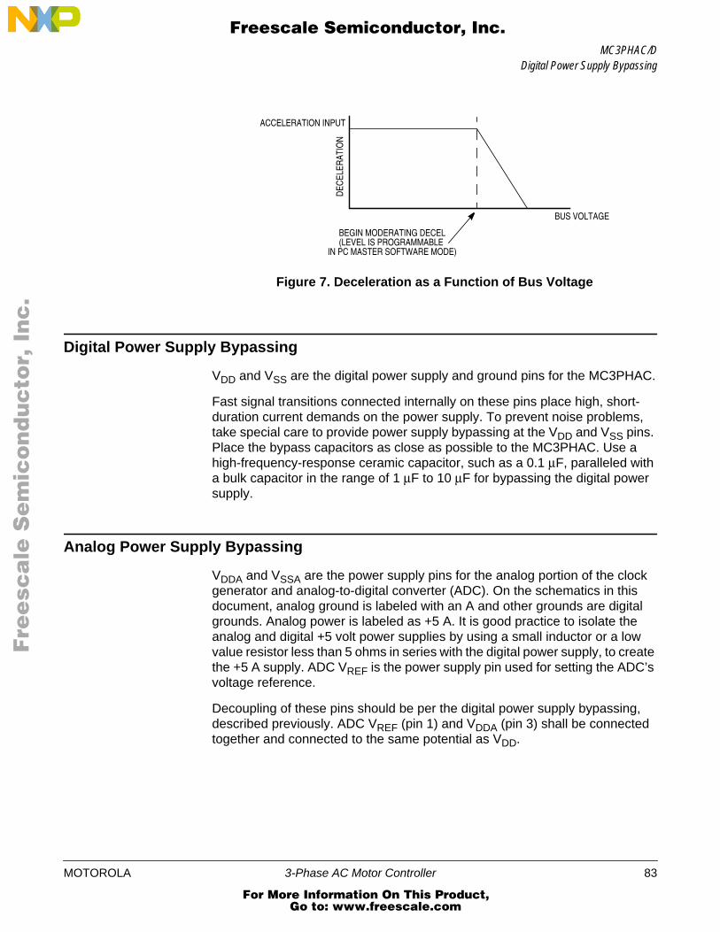
MC3PHAC/DDigital Power Supply Bypassing
F
ree
sca
le S
em
ico
nd
uc
tor,
I
Freescale Semiconductor, Inc.n
c..
.
Figure 7. Deceleration as a Function of Bus VoltageDigital Power Supply Bypassing
VDD and VSS are the digital power supply and ground pins for the MC3PHAC.
Fast signal transitions connected internally on these pins place high, short-duration current demands on the power supply. To prevent noise problems,take special care to provide power supply bypassing at the VDD and VSS pins.Place the bypass capacitors as close as possible to the MC3PHAC. Use ahigh-frequency-response ceramic capacitor, such as a 0.1 µF, paralleled witha bulk capacitor in the range of 1 µF to 10 µF for bypassing the digital powersupply.
Analog Power Supply Bypassing
VDDA and VSSA are the power supply pins for the analog portion of the clockgenerator and analog-to-digital converter (ADC). On the schematics in thisdocument, analog ground is labeled with an A and other grounds are digitalgrounds. Analog power is labeled as +5 A. It is good practice to isolate theanalog and digital +5 volt power supplies by using a small inductor or a lowvalue resistor less than 5 ohms in series with the digital power supply, to createthe +5 A supply. ADC VREF is the power supply pin used for setting the ADC’svoltage reference.
Decoupling of these pins should be per the digital power supply bypassing,described previously. ADC VREF (pin 1) and VDDA (pin 3) shall be connectedtogether and connected to the same potential as VDD.
BUS VOLTAGE
ACCELERATION INPUT
DEC
ELER
ATIO
N
BEGIN MODERATING DECEL(LEVEL IS PROGRAMMABLE
IN PC MASTER SOFTWARE MODE)
MOTOROLA 3-Phase AC Motor Controller 83
For More Information On This Product, Go to: www.freescale.com
MC3PHAC/D
F
ree
sca
le S
em
ico
nd
uc
tor,
I
Freescale Semiconductor, Inc.n
c..
.
Grounding Considerations
Printed circuit board layout is an important design consideration. In particular,ground planes and how grounds are tied together influence noise immunity. Tomaximize noise immunity, it is important to get a good ground plane under theMC3PHAC. It is also important to separate analog and digital grounds. That iswhy, shown on the schematics, there are two ground designations, analogground is marked with an A and other grounds are digital grounds. GND is thedigital ground plane and power supply return. GNDA is the analog circuitground. They are both the same reference voltage, but are routed separately,and tie together at only one point.
Power-Up/Power-Down
When power is applied or removed, it is important that the inverter’s top andbottom output transistors in the same phase are not turned on simultaneously.Since logic states are not always defined during power-up, it is important toensure that all power transistors remain off when the controller’s supply voltageis below its normal operating level. The MC3PHAC’s PWM module outputsmake this easy by switching to a high impedance configuration whenever the5-volt supply is below its specified minimum.
The user should use pullup or pulldown resistors on the output of theMC3PHAC’s PWM outputs to ensure during power-up and power-down, thatthe inverter’s drive inputs are at a known, turned off, state.
Operation
The MC3PHAC motor controller will operate in two modes. The first isstandalone operation, whereby the MC3PHAC can be used without anyintervention from an external personal computer. In standalone mode, theMC3PHAC is initialized by passive devices connected to the MC3PHAC andinput to the system at power-up/reset time. In standalone mode, someparameters continue to be input to the system as it operates. Speed, PWMfrequency, bus voltage, and acceleration parameters are input to the systemon a real-time basis.
The second mode of operation is called PC master software mode.Thatoperational mode requires the use of a personal computer and PC mastersoftware executing on the personal computer, communicating with theMC3PHAC, or a microcontroller emulating PC master software commands.All command and setup information is input to the MC3PHAC via the PC host.
84 3-Phase AC Motor Controller MOTOROLA
For More Information On This Product, Go to: www.freescale.com

MC3PHAC/DOperation
F
ree
sca
le S
em
ico
nd
uc
tor,
I
Freescale Semiconductor, Inc.n
c..
.
Standalone Operation
If the VBOOST_MODE pin is high when the MC3PHAC is powered up, or aftera reset, the MC3PHAC enters standalone mode. In this mode of operation, thefunctionality of many of the MC3PHAC pins change so that the device cancontrol a motor without requiring setup information from an external master.When operated in standalone mode, the MC3PHAC will drive certain pinscorresponding to parameters which must be specified, while simultaneouslymonitoring the response on other pins.
In many cases, the parameter to be specified is represented as an analogvoltage presented to the MUX_IN pin, while certain other pins are driven low.In so doing, the MC3PHAC can accommodate an external analog mux whichwill switch various signals on the MUX_IN pin when the signal select line goeslow. All signals must be in a range between 0 V and VREF. As an economicalalternative, an external passive network can be connected to each of theparameter select output pins and the MUX_IN pin, as shown in Figure 8.
The Thevenin equivalent impedance of this passive network as seen by theMUX_IN pin is very important and should be in the range of 5 kΩ to 10 kΩ. Ifthe resistance is too high, leakage current from the input/output (I/O) pins willcause an offset voltage that will affect the accuracy of the reading. If theresistance is too low, the parameter select pins will not be able to sink therequired current for an accurate reading. Using a pullup resistor value of 6.8 kΩ(as indicated in Figure 8), the resulting value for each parameter as a functionof the corresponding pulldown resistor value is shown in Figure 9, Figure 10,Figure 11, and Table 4.
The START input pin is debounced internally and a switch can be directlyaccommodated on this pin. The input is level sensitive, but a logic 1 level mustexist on the pin before a logic 0 level will be processed as a start signal. Thiswill prevent an accidental motor startup in the event of the MC3PHAC beingpowered up, where the switch was left in the start position.
The FWD input pin is debounced internally and can directly accommodate aswitch connection. The input is also level sensitive.
Figure 8 shows the jumper arrangement connected to thePWMPOL_BASEFREQ input pin. For proper operation, one and only onejumper connection can be made at any given time. Table 3 shows the polarityand base frequency selections as a function of the jumper connection.
MOTOROLA 3-Phase AC Motor Controller 85
For More Information On This Product, Go to: www.freescale.com
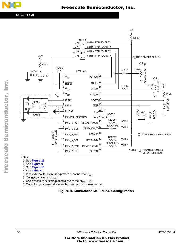
MC3PHAC/D
F
ree
sca
le S
em
ico
nd
uc
tor,
I
Freescale Semiconductor, Inc.n
c..
.
Figure 8. Standalone MC3PHAC Configuration
Notes:1. See Figure 11.2. See Figure 9.3. See Figure 10.4. See Table 4.5. If no external fault circuit is provided, connect to VSS.6. Connect only one jumper.7. Use bypass capacitors placed close to the MC3PHAC.8. Consult crystal/resonator manufacturer for component values.
JP1
JP2
JP3
JP4
22 pF
22 pF 4.0
MH
z
1
2
3
4
5
6
7
8
9
10
11
12
13
14
28
27
26
25
24
23
22
21
20
19
18
17
16
15
FROM DIVIDED DC BUS
+5 V
6.8 kΩNOTE 6
50 Hz – PWM POLARITY
50 Hz + PWM POLARITY
60 Hz – PWM POLARITY
60 Hz + PWM POLARITY+5 V
10 kΩ
RESET 0.1 µF
NOTE 7+5 A
6 —
PW
Ms
TOPO
WER
STA
GE
MC3PHAC
+5 A
5 kΩ
A
ACC
ELER
ATIO
N P
OT
4.7 kΩ
A
+5 A
5 kΩ
A
SPEE
D P
OT
+5 V
10 kΩ
STAR
T/ST
OP
FOR
/REV10 kΩ
+ 5+ 5
NOTE 7
NOTE 1
NOTE 2
NOTE 3
NOTE 4
FROM SYSTEM FAULTDETECTION CIRCUIT
TO RESISTIVE BRAKE DRIVER
VREF
RESET
VDDA
VSSA
OSC2
OSC1
PLLCAP
PWMPOL_BASEFREQ
PWM_U_TOP
PWM_U_BOT
PWM_V_TOP
PWM_V_BOT
PWM_W_TOP
PWM_W_BOT
DC_BUS
ACCEL
SPEED
MUX_IN
START
FWD
VSS
VDD
VBOOST_MODE
DT_FAULTOUT
RBRAKE
RETRY/TxD
PWMFREQ/RxD
FAULTIN NOTE 5
4.7 kΩ
0.1 µF
RPWMFREQ
RRETRY
RDEADTIME
RBOOST
NOTE 8
10 MΩ
86 3-Phase AC Motor Controller MOTOROLA
For More Information On This Product, Go to: www.freescale.com
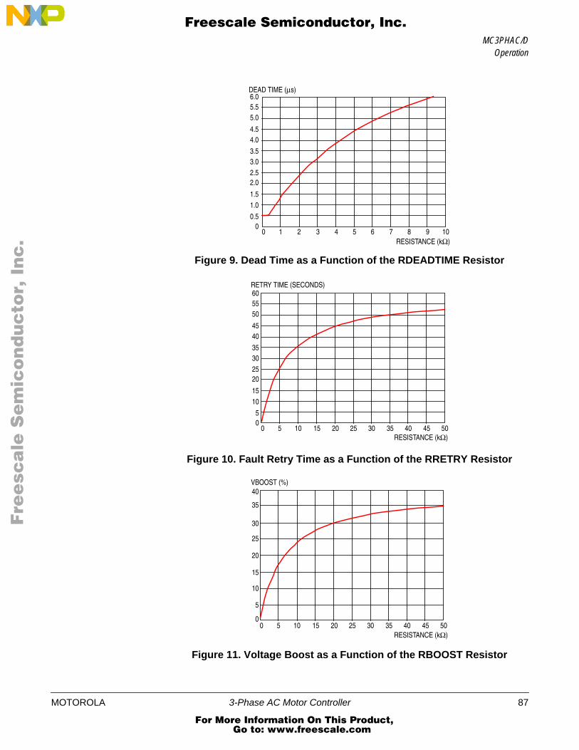
MC3PHAC/DOperation
F
ree
sca
le S
em
ico
nd
uc
tor,
I
Freescale Semiconductor, Inc.n
c..
.
Figure 9. Dead Time as a Function of the RDEADTIME Resistor
Figure 10. Fault Retry Time as a Function of the RRETRY Resistor
Figure 11. Voltage Boost as a Function of the RBOOST Resistor
6.05.55.0
4.54.0
3.53.02.52.0
1.51.0
0.50
0 1 2 3 4 5 6 7 8 9 10
DEAD TIME (µs)
RESISTANCE (kΩ)
605550
4540
35302520
1510
50
0 5 10 15 20 25 30 35 40 45 50
RETRY TIME (SECONDS)
RESISTANCE (kΩ)
40
35
30
25
20
15
5
00 5 10 15 20 25 30 35 40 45 50
VBOOST (%)
RESISTANCE (kΩ)
10
MOTOROLA 3-Phase AC Motor Controller 87
For More Information On This Product, Go to: www.freescale.com
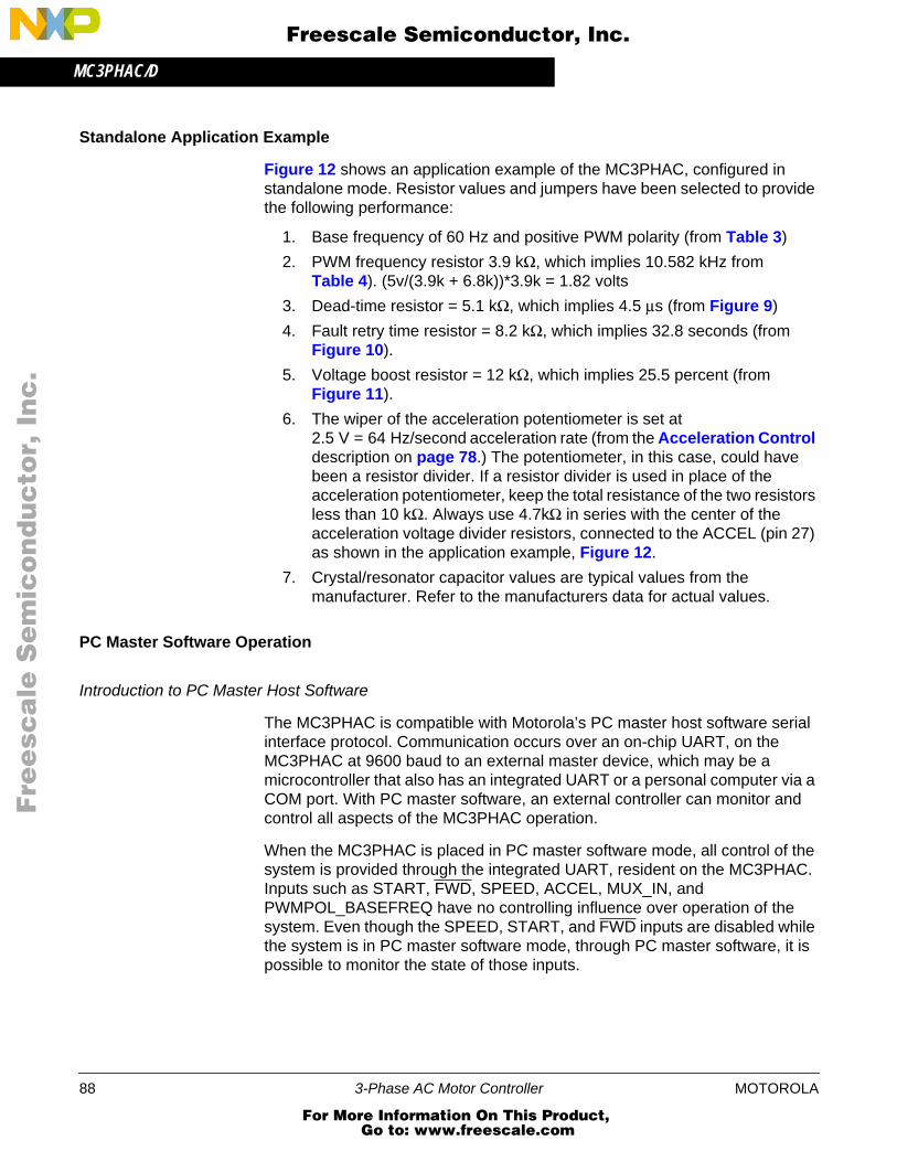
MC3PHAC/D
F
ree
sca
le S
em
ico
nd
uc
tor,
I
Freescale Semiconductor, Inc.n
c..
.
Standalone Application Example
Figure 12 shows an application example of the MC3PHAC, configured instandalone mode. Resistor values and jumpers have been selected to providethe following performance:
1. Base frequency of 60 Hz and positive PWM polarity (from Table 3)
2. PWM frequency resistor 3.9 kΩ, which implies 10.582 kHz fromTable 4). (5v/(3.9k + 6.8k))*3.9k = 1.82 volts
3. Dead-time resistor = 5.1 kΩ, which implies 4.5 µs (from Figure 9)
4. Fault retry time resistor = 8.2 kΩ, which implies 32.8 seconds (fromFigure 10).
5. Voltage boost resistor = 12 kΩ, which implies 25.5 percent (fromFigure 11).
6. The wiper of the acceleration potentiometer is set at2.5 V = 64 Hz/second acceleration rate (from the Acceleration Controldescription on page 78.) The potentiometer, in this case, could havebeen a resistor divider. If a resistor divider is used in place of theacceleration potentiometer, keep the total resistance of the two resistorsless than 10 kΩ. Always use 4.7kΩ in series with the center of theacceleration voltage divider resistors, connected to the ACCEL (pin 27)as shown in the application example, Figure 12.
7. Crystal/resonator capacitor values are typical values from themanufacturer. Refer to the manufacturers data for actual values.
PC Master Software Operation
Introduction to PC Master Host Software
The MC3PHAC is compatible with Motorola’s PC master host software serialinterface protocol. Communication occurs over an on-chip UART, on theMC3PHAC at 9600 baud to an external master device, which may be amicrocontroller that also has an integrated UART or a personal computer via aCOM port. With PC master software, an external controller can monitor andcontrol all aspects of the MC3PHAC operation.
When the MC3PHAC is placed in PC master software mode, all control of thesystem is provided through the integrated UART, resident on the MC3PHAC.Inputs such as START, FWD, SPEED, ACCEL, MUX_IN, andPWMPOL_BASEFREQ have no controlling influence over operation of thesystem. Even though the SPEED, START, and FWD inputs are disabled whilethe system is in PC master software mode, through PC master software, it ispossible to monitor the state of those inputs.
88 3-Phase AC Motor Controller MOTOROLA
For More Information On This Product, Go to: www.freescale.com
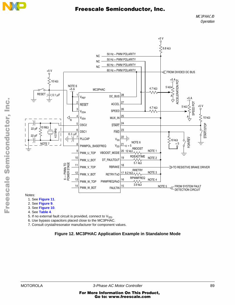
MC3PHAC/DOperation
F
ree
sca
le S
em
ico
nd
uc
tor,
I
Freescale Semiconductor, Inc.n
c..
.
Figure 12. MC3PHAC Application Example in Standalone Mode
Notes:1. See Figure 11.2. See Figure 9.3. See Figure 10.4. See Table 4.5. If no external fault circuit is provided, connect to VSS.6. Use bypass capacitors placed close to the MC3PHAC.7. Consult crystal/resonator manufacturer for component values.
22 pF
22 pF 4.0
MH
z
1
2
3
4
5
6
7
8
9
10
11
12
13
14
28
27
26
25
24
23
22
21
20
19
18
17
16
15
FROM DIVIDED DC BUS
+5 V
6.8 kΩ
50 Hz – PWM POLARITY
50 Hz + PWM POLARITY
60 Hz – PWM POLARITY
60 Hz + PWM POLARITY+5 V
10 kΩ
RESET 0.1 µF
NOTE 6+5 A
6 —
PW
Ms
TOPO
WER
STA
GE
MC3PHAC
+5 A
5 kΩ
A
ACC
ELER
ATIO
N P
OT
4.7 kΩ
A
+5 A
5 kΩ
A
SPEE
D P
OT
+5 V
10 kΩ
STAR
T/ST
OP
FOR
/REV10 kΩ
+ 5+ 5
NOTE 6
NOTE 1
NOTE 2
NOTE 3
NOTE 4
FROM SYSTEM FAULTDETECTION CIRCUIT
TO RESISTIVE BRAKE DRIVER
VREF
RESET
VDDA
VSSA
OSC2
OSC1
PLLCAP
PWMPOL_BASEFREQ
PWM_U_TOP
PWM_U_BOT
PWM_V_TOP
PWM_V_BOT
PWM_W_TOP
PWM_W_BOT
DC_BUS
ACCEL
SPEED
MUX_IN
START
FWD
VSS
VDD
VBOOST_MODE
DT_FAULTOUT
RBRAKE
RETRY/TxD
PWMFREQ/RxD
FAULTIN NOTE 5
4.7 kΩ
0.1 µF
RPWMFREQ
RRETRY
RDEADTIME
RBOOST
NOTE 7
10 MΩ
NC
NC
NC
12 kΩ
5.1 kΩ
8.2 kΩ
3.9 kΩ
MOTOROLA 3-Phase AC Motor Controller 89
For More Information On This Product, Go to: www.freescale.com

MC3PHAC/D
F
ree
sca
le S
em
ico
nd
uc
tor,
I
Freescale Semiconductor, Inc.n
c..
.
The most popular master implementation is a PC, where a graphical userinterface (GUI) has been layered on top of the PC master software commandprotocol, complete with a graphical data display, and an ActiveX interface.Figure 13 shows the MC3PHAC configured in PC master software mode. It isbeyond the scope of this document to describe the PC master softwareprotocol or its implementation on a personal computer. For further informationon these topics, refer to other Motorola documents relating to the PC mastersoftware protocol and availability of PC master host software.
Figure 13. MC3PHAC Configuration for Using a PC as a Master
Notes:1. If no external fault circuit is provided, connect to VSS.2. Use bypass capacitors placed close to the MC3PHAC.3. Consult crystal/resonator manufacturer for component values.
22 pF
22 pF 4.0
MH
z
1
2
3
4
5
6
7
8
9
10
11
12
13
14
28
27
26
25
24
23
22
21
20
19
18
17
16
15
FROM DIVIDED DC BUS
+5 V
10 kΩ
RESET 0.1 µF
NOTE 2+5 A
6 —
PW
Ms
TOPO
WER
STA
GE
MC3PHAC
A
+ 5NOTE 2
FROM SYSTEM FAULTDETECTION CIRCUIT
TO RESISTIVE BRAKE DRIVER
VREF
RESET
VDDA
VSSA
OSC2
OSC1
PLLCAP
PWMPOL_BASEFREQ
PWM_U_TOP
PWM_U_BOT
PWM_V_TOP
PWM_V_BOT
PWM_W_TOP
PWM_W_BOT
DC_BUS
ACCEL
SPEED
MUX_IN
START
FWD
VSS
VDD
VBOOST_MODE
DT_FAULTOUT
RBRAKE
RETRY/TxD
PWMFREQ/RxD
FAULTIN
10 kΩ
0.1 µFNOTE 3
10 MΩ
+5 V10 kΩ
+5 V
FAULT LED
560 Ω
DATA TO PC
DATA FROM PCISOLATED
OR NON-ISOLATEDRS232 INTERFACE
CONNECTIONTO HOST
NOTE 1
90 3-Phase AC Motor Controller MOTOROLA
For More Information On This Product, Go to: www.freescale.com
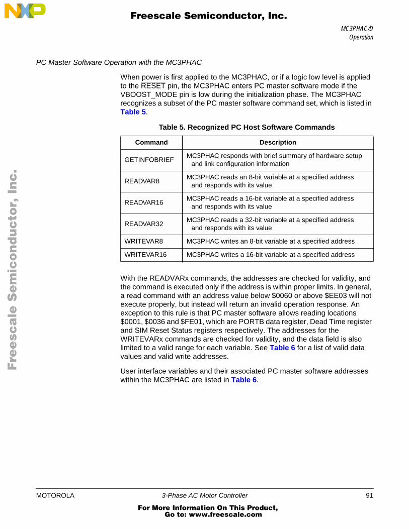
MC3PHAC/DOperation
F
ree
sca
le S
em
ico
nd
uc
tor,
I
Freescale Semiconductor, Inc.n
c..
.
PC Master Software Operation with the MC3PHAC
When power is first applied to the MC3PHAC, or if a logic low level is appliedto the RESET pin, the MC3PHAC enters PC master software mode if theVBOOST_MODE pin is low during the initialization phase. The MC3PHACrecognizes a subset of the PC master software command set, which is listed inTable 5.
With the READVARx commands, the addresses are checked for validity, andthe command is executed only if the address is within proper limits. In general,a read command with an address value below $0060 or above $EE03 will notexecute properly, but instead will return an invalid operation response. Anexception to this rule is that PC master software allows reading locations$0001, $0036 and $FE01, which are PORTB data register, Dead Time registerand SIM Reset Status registers respectively. The addresses for theWRITEVARx commands are checked for validity, and the data field is alsolimited to a valid range for each variable. See Table 6 for a list of valid datavalues and valid write addresses.
User interface variables and their associated PC master software addresseswithin the MC3PHAC are listed in Table 6.
Table 5. Recognized PC Host Software Commands
Command Description
GETINFOBRIEFMC3PHAC responds with brief summary of hardware setup
and link configuration information
READVAR8MC3PHAC reads an 8-bit variable at a specified address
and responds with its value
READVAR16MC3PHAC reads a 16-bit variable at a specified address
and responds with its value
READVAR32MC3PHAC reads a 32-bit variable at a specified address
and responds with its value
WRITEVAR8 MC3PHAC writes an 8-bit variable at a specified address
WRITEVAR16 MC3PHAC writes a 16-bit variable at a specified address
MOTOROLA 3-Phase AC Motor Controller 91
For More Information On This Product, Go to: www.freescale.com
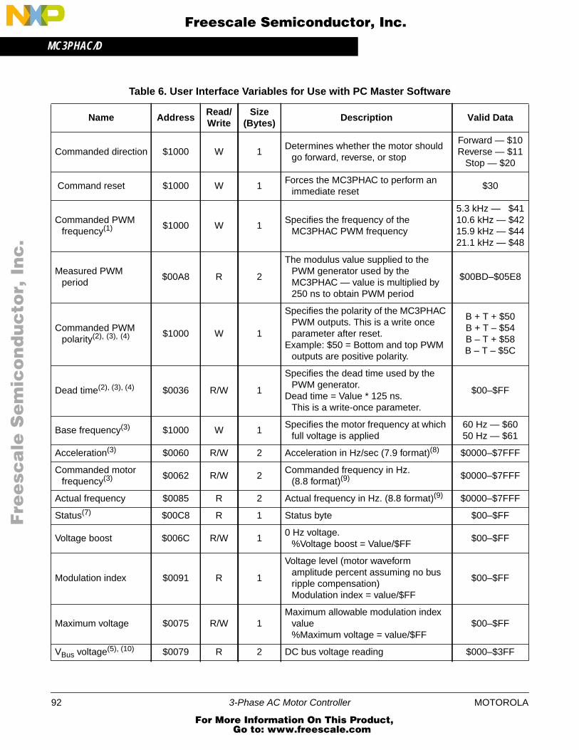
MC3PHAC/D
F
ree
sca
le S
em
ico
nd
uc
tor,
I
Freescale Semiconductor, Inc.n
c..
.
Table 6. User Interface Variables for Use with PC Master Software
Name AddressRead/Write
Size(Bytes)
Description Valid Data
Commanded direction $1000 W 1Determines whether the motor should
go forward, reverse, or stop
Forward — $10Reverse — $11
Stop — $20
Command reset $1000 W 1Forces the MC3PHAC to perform an
immediate reset$30
Commanded PWMfrequency(1) $1000 W 1
Specifies the frequency of theMC3PHAC PWM frequency
5.3 kHz — $4110.6 kHz — $4215.9 kHz — $4421.1 kHz — $48
Measured PWMperiod
$00A8 R 2
The modulus value supplied to thePWM generator used by theMC3PHAC — value is multiplied by250 ns to obtain PWM period
$00BD–$05E8
Commanded PWMpolarity(2), (3), (4) $1000 W 1
Specifies the polarity of the MC3PHACPWM outputs. This is a write onceparameter after reset.
Example: $50 = Bottom and top PWMoutputs are positive polarity.
B + T + $50B + T – $54B – T + $58B – T – $5C
Dead time(2), (3), (4) $0036 R/W 1
Specifies the dead time used by thePWM generator.
Dead time = Value * 125 ns.This is a write-once parameter.
$00–$FF
Base frequency(3) $1000 W 1Specifies the motor frequency at which
full voltage is applied60 Hz — $6050 Hz — $61
Acceleration(3) $0060 R/W 2 Acceleration in Hz/sec (7.9 format)(8) $0000–$7FFF
Commanded motorfrequency(3) $0062 R/W 2
Commanded frequency in Hz.(8.8 format)(9) $0000–$7FFF
Actual frequency $0085 R 2 Actual frequency in Hz. (8.8 format)(9) $0000–$7FFF
Status(7) $00C8 R 1 Status byte $00–$FF
Voltage boost $006C R/W 10 Hz voltage.
%Voltage boost = Value/$FF$00–$FF
Modulation index $0091 R 1
Voltage level (motor waveformamplitude percent assuming no busripple compensation)Modulation index = value/$FF
$00–$FF
Maximum voltage $0075 R/W 1Maximum allowable modulation index
value%Maximum voltage = value/$FF
$00–$FF
VBus voltage(5), (10) $0079 R 2 DC bus voltage reading $000–$3FF
92 3-Phase AC Motor Controller MOTOROLA
For More Information On This Product, Go to: www.freescale.com

MC3PHAC/DOperation
F
ree
sca
le S
em
ico
nd
uc
tor,
I
Freescale Semiconductor, Inc.n
c..
.
Fault timeout $006A R/W 2
Specifies the delay time after a faultcondition before re-enabling themotor.
Fault timeout = value * 0.262 sec
$0000–$FFFF
Fault timer $006D R 2Real-time display of the fault timerElapsed fault time = value * 0.262 sec
$0000–$FFFF
VBus decel value(10) $00C9 R/W 2VBus readings above this value result in
reduced deceleration.$0000–$03FF
VBus RBRAKEvalue(10) $0064 R/W 2
VBus readings above this value result inthe RBRAKE pin being asserted.
$0000–$03FF
VBus brownoutvalue(10) $0066 R/W 2
VBus readings below this value result inan under voltage fault.
$0000–$03FF
VBus over voltagevalue(10) $0068 R/W 2
VBus readings above this value result inan over voltage fault.
$0000–$03FF
Speed in ADCvalue(5) $0095 R 2
Left justified 10-bit ADC reading of theSPEED input pin.
$0000–$FFC0
Setup(7) $00AE R 1Bit field indicating which setup
parameters have been initializedbefore motion is permitted
$E0–$FF
Switch in(7) $0001 R 1Bit field indicating the current state of
the start/stop and forward/reverseswitches
$00–$FF
Reset status(6), (7) $FE01 R 1 Indicates cause of the last reset $00–$FF
Version $EE00 R 4 MC3PHAC version ASCII field
1. The commanded PWM frequency cannot be written until the PWM outputs exit the high-impedance state. The default PWMfrequency is 15.873 kHz.
2. The PWM output pins remain in a high-impedance state until this parameter is specified.3. This parameter must be specified before motor motion can be initiated by the MC3PHAC.4. This is a write-once parameter. The first write to this address will execute normally. Further attempts at writing this
parameter will result in an illegal operation response from the MC3PHAC.5. The value of this parameter is not valid until the PWM outputs exit the high-impedance state.6. The data in this field is only valid for one read. Further reads will return a value of $00.7. See register bit descriptions following this table.8. Acceleration is an unsigned value with the upper seven bits range of $00 to $7F = acceleration value of 0 to
127 Hertz/second. The lower nine bits constitute the fractional portion of the acceleration parameter. Its range is $000 to$1FF which equals 0 to ~1. Therefore, the range of acceleration is 0 to 127.99 Hertz/second.
9. Commanded motor frequency and actual frequency are signed values with the upper byte range of$00 to $7F = frequency of 0 to 127 Hz. The lower byte is the fractional portion of the frequency. Its range is $00 to $FFwhich equals 0 to ~1.
10. VBus is the voltage value applied to the DC_BUS analog input pin. The analog-to-digital converter is a 10-bit converter witha 5 volt full scale input. The value is equal to the voltage applied to the DC_BUS input pin/VREF * $03FF.
Table 6. User Interface Variables for Use with PC Master Software (Continued)
Name AddressRead/Write
Size(Bytes)
Description Valid Data
MOTOROLA 3-Phase AC Motor Controller 93
For More Information On This Product, Go to: www.freescale.com
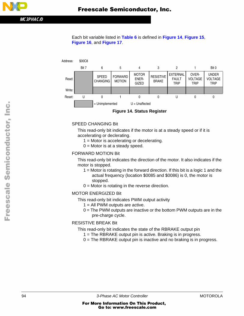
MC3PHAC/D
F
ree
sca
le S
em
ico
nd
uc
tor,
I
Freescale Semiconductor, Inc.n
c..
.
Each bit variable listed in Table 6 is defined in Figure 14, Figure 15,Figure 16, and Figure 17.
SPEED CHANGING Bit
This read-only bit indicates if the motor is at a steady speed or if it isaccelerating or declerating.
1 = Motor is accelerating or decelerating.0 = Motor is at a steady speed.
FORWARD MOTION Bit
This read-only bit indicates the direction of the motor. It also indicates if themotor is stopped.
1 = Motor is rotating in the forward direction. If this bit is a logic 1 and theactual frequency (location $0085 and $0086) is 0, the motor isstopped.
0 = Motor is rotating in the reverse direction.
MOTOR ENERGIZED Bit
This read-only bit indicates PWM output activity1 = All PWM outputs are active.0 = The PWM outputs are inactive or the bottom PWM outputs are in the
pre-charge cycle.
RESISTIVE BREAK Bit
This read-only bit indicates the state of the RBRAKE output pin1 = The RBRAKE output pin is active. Braking is in progress.0 = The RBRAKE output pin is inactive and no braking is in progress.
Address: $00C8
Bit 7 6 5 4 3 2 1 Bit 0
Read:SPEED
CHANGINGFORWARD
MOTION
MOTORENER-GIZED
RESISTIVEBRAKE
EXTERNALFAULTTRIP
OVER-VOLTAGE
TRIP
UNDERVOLTAGE
TRIP
Write:
Reset: U 0 1 0 0 U 0 0
= Unimplemented U = Unaffected
Figure 14. Status Register
94 3-Phase AC Motor Controller MOTOROLA
For More Information On This Product, Go to: www.freescale.com
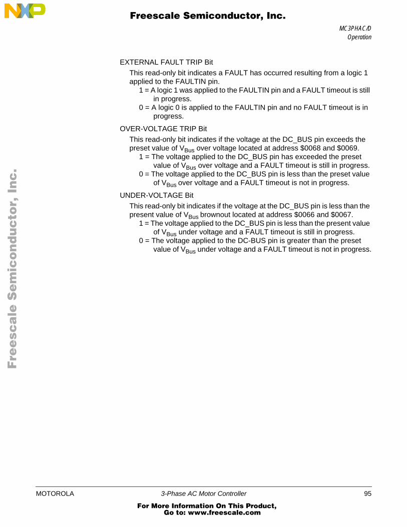
MC3PHAC/DOperation
F
ree
sca
le S
em
ico
nd
uc
tor,
I
Freescale Semiconductor, Inc.n
c..
.
EXTERNAL FAULT TRIP Bit
This read-only bit indicates a FAULT has occurred resulting from a logic 1applied to the FAULTIN pin.
1 = A logic 1 was applied to the FAULTIN pin and a FAULT timeout is stillin progress.
0 = A logic 0 is applied to the FAULTIN pin and no FAULT timeout is inprogress.
OVER-VOLTAGE TRIP Bit
This read-only bit indicates if the voltage at the DC_BUS pin exceeds thepreset value of VBus over voltage located at address $0068 and $0069.
1 = The voltage applied to the DC_BUS pin has exceeded the presetvalue of VBus over voltage and a FAULT timeout is still in progress.
0 = The voltage applied to the DC_BUS pin is less than the preset valueof VBus over voltage and a FAULT timeout is not in progress.
UNDER-VOLTAGE Bit
This read-only bit indicates if the voltage at the DC_BUS pin is less than thepresent value of VBus brownout located at address $0066 and $0067.
1 = The voltage applied to the DC_BUS pin is less than the present valueof VBus under voltage and a FAULT timeout is still in progress.
0 = The voltage applied to the DC-BUS pin is greater than the presetvalue of VBus under voltage and a FAULT timeout is not in progress.
MOTOROLA 3-Phase AC Motor Controller 95
For More Information On This Product, Go to: www.freescale.com
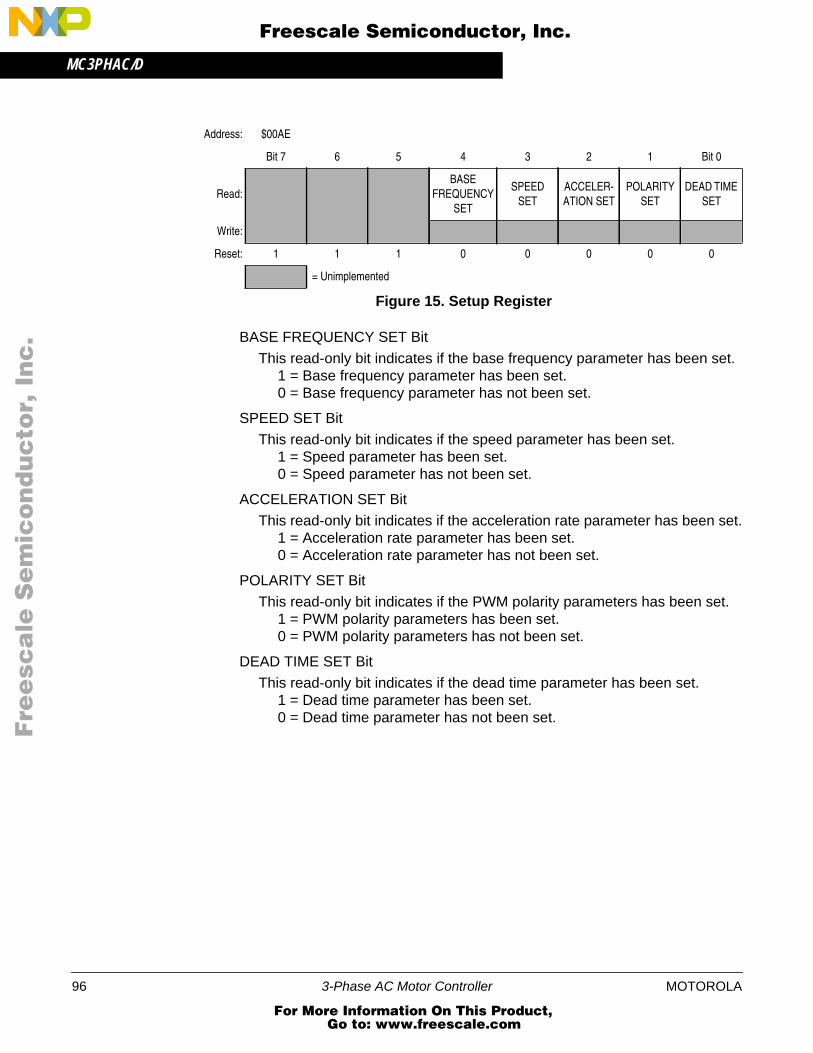
MC3PHAC/D
F
ree
sca
le S
em
ico
nd
uc
tor,
I
Freescale Semiconductor, Inc.n
c..
.
BASE FREQUENCY SET Bit
This read-only bit indicates if the base frequency parameter has been set.1 = Base frequency parameter has been set.0 = Base frequency parameter has not been set.
SPEED SET Bit
This read-only bit indicates if the speed parameter has been set.1 = Speed parameter has been set.0 = Speed parameter has not been set.
ACCELERATION SET Bit
This read-only bit indicates if the acceleration rate parameter has been set.1 = Acceleration rate parameter has been set.0 = Acceleration rate parameter has not been set.
POLARITY SET Bit
This read-only bit indicates if the PWM polarity parameters has been set.1 = PWM polarity parameters has been set.0 = PWM polarity parameters has not been set.
DEAD TIME SET Bit
This read-only bit indicates if the dead time parameter has been set.1 = Dead time parameter has been set.0 = Dead time parameter has not been set.
Address: $00AE
Bit 7 6 5 4 3 2 1 Bit 0
Read:BASE
FREQUENCYSET
SPEEDSET
ACCELER-ATION SET
POLARITYSET
DEAD TIMESET
Write:
Reset: 1 1 1 0 0 0 0 0
= Unimplemented
Figure 15. Setup Register
96 3-Phase AC Motor Controller MOTOROLA
For More Information On This Product, Go to: www.freescale.com
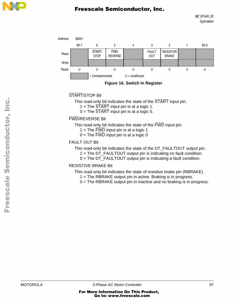
MC3PHAC/DOperation
F
ree
sca
le S
em
ico
nd
uc
tor,
I
Freescale Semiconductor, Inc.n
c..
.
START/STOP BitThis read-only bit indicates the state of the START input pin.1 = The START input pin is at a logic 1.0 = The START input pin is at a logic 0.
FWD/REVERSE Bit
This read-only bit indicates the state of the FWD input pin.1 = The FWD input pin is at a logic 10 = The FWD input pin is at a logic 0
FAULT OUT Bit
This read-only bit indicates the state of the DT_FAULTOUT output pin.1 = The DT_FAULTOUT output pin is indicating no fault condition.0 = The DT_FAULTOUT output pin is indicating a fault condition.
RESISTIVE BRAKE Bit
This read-only bit indicates the state of resistive brake pin (RBRAKE).1 = The RBRAKE output pin in active. Braking is in progress.0 = The RBRAKE output pin in inactive and no braking is in progress.
Address: $0001
Bit 7 6 5 4 3 2 1 Bit 0
Read:START/STOP
FWD/REVERSE
FAULTOUT
RESISTORBRAKE
Write:
Reset: U U U U U 0 U U
= Unimplemented U = Unaffected
Figure 16. Switch In Register
MOTOROLA 3-Phase AC Motor Controller 97
For More Information On This Product, Go to: www.freescale.com

MC3PHAC/D
F
ree
sca
le S
em
ico
nd
uc
tor,
I
Freescale Semiconductor, Inc.n
c..
.
POWER UP BitThis read-only bit indicates the last system reset was caused by the power-up reset detection circuit.
1 = The last reset was caused by an initial power-up of the MC3PHAC.0 = Power-up reset was not the source of the reset or a read of the reset
status register after the first read.
RESET PIN BitThis read-only bit indicates the last system reset was caused from theRESET input pin.
1 = Last reset was caused by an external reset applied to the RESETinput pin.
0 = The RESET pin was not the source of the reset or a read of the resetstatus register after the first read.
MC3PHAC FUNCTIONAL FAULT BitsThis read-only bit indicates if the last system reset was the result of aninternal system error.
1 = MC3PHAC internal system error0 = The FUNCTIONAL FAULT was not the source of the reset or a read
of the reset status register after the first read.
PC MASTER SOFTWARE RESET COMMAND BitThis read-only bit indicates the last system reset was the result of a PCmaster software reset command.
1 = The MC3PHAC was reset by the PC master software command resetas the result of a write of $30 to location $1000
0 = The PC master software RESET COMMAND was not the source ofthe reset or a read of the reset status register after the first read.
LOW VDD VOLTAGE Bit
This read-only bit indicates if the last reset was the result of low VDD appliedto the MC3PHAC.
1 = The last reset was caused by the low power supply detection circuit.0 = The LOW VDD was not the source of the reset or a read of the reset
status register after the first read.
Address: $FE01
Bit 7 6 5 4 3 2 1 Bit 0
Read:POWER
UPRESET
PIN
MC3PHACFUNCTIONAL
FAULT
MC3PHACFUNCTIONAL
FAULT
PCMASTERSOFTWARE
RESETCOMMAND
LOW VDDVOLTAGE
Write:
Reset: 1 0 0 0 0 0 0 0
= Unimplemented
Figure 17. Reset Status Register
98 3-Phase AC Motor Controller MOTOROLA
For More Information On This Product, Go to: www.freescale.com
MC3PHAC/DOperation
F
ree
sca
le S
em
ico
nd
uc
tor,
I
Freescale Semiconductor, Inc.n
c..
.
Command State Machine
When using the PC master software mode of operation, the command statemachine governs behavior of the device depending upon its current state,system parameters, any new commands received via the communications link,and the prevailing conditions of the system. The command state diagram is inFigure 18. It illustrates the sequence of commands which are necessary tobring the device from the reset condition to running the motor in a steady stateand depicts the permissible state transitions. The device will remain within agiven state unless the conditions shown for a transition are met.
Some commands only cause a temporary state change to occur. While theyare being executed, the state machine will automatically return to the statewhich existed prior to the command being received. For example, the motorspeed may be changed from within any state by using the WRITEVAR16command to write to the "Speed In" variable. This will cause the "Set Speed"state to be momentarily entered, the "Speed In" variable will be updated andthen the original state will be re-entered. This allows the motor speed,acceleration or base frequency to be modified whether the motor is alreadyaccelerating, decelerating, or in a steady state.
Each state is described here in more detail.
• Reset — This state is entered when a device power-on reset (POR), pinreset, loss of crystal, internally detected error, or reset command occursfrom within any state. In this state, the device is initialized and the PWMoutputs are configured to high impedance. This state is thenautomatically exited.
• PWMHighZ — This state is entered from the reset state. This state isalso re-entered after one and only one of the PWM dead-time or polarityparameters have been initialized. In this state the PWM outputs areconfigured to a high-impedance state as the device waits for both thePWM dead time and polarity to be initialized.
• SetDeadTime (write once) — This state is entered from the PWMHighZstate the first time that a write to the PWM dead-time variable occurs. Inthis state, the PWM dead time is initialized and the state is thenautomatically exited. This state cannot be re-entered, and hence thedead time cannot be modified, unless the reset state is first re-entered.
• SetPolarity (write once) — This state is entered from the PWMHighZstate the first time that the PWM polarity command is received. In thisstate, the PWM polarity is initialized and the state is then automaticallyexited. This state cannot be re-entered, and hence the polarity cannotbe modified, unless the reset state is first re-entered.
MOTOROLA 3-Phase AC Motor Controller 99
For More Information On This Product, Go to: www.freescale.com

MC3PHAC/D
F
ree
sca
le S
em
ico
nd
uc
tor,
I
Freescale Semiconductor, Inc.n
c..
.
Figure 18. PC Host Software Command State Diagram
PWMHighZ
Reset
FwdDecel FwdAccel
PWM0RPM
SetPolarity(write once)
SetDeadTime(write once)
FwdSteady
RevAccel RevDecel
RevSteady
CmdReset Reset orPOR orLoss of Crystal orInternal Error
Initialized
CmdPWMTxBx
done
done
WRITEVAR8:Dead-time
PWM base freq. set &Acceleration set &Speed In set
CmdStop&
Actual speed = 0
CmdRev|CmdStop
CmdFwd|CmdStop
Actual speed =Speed In
Actual speed =Speed In
Speed In >Actual Speed
Speed In >Actual Speed
(Spee
d In <
Act
ual sp
eed) |
CmdFwd| C
mdSto
p
(Speed In < Actual speed) |
CmdRev| CmdStop
SetSpeed
WRITEVAR16:SpeedIn from any state
Done(return tocallingstate)
SetSpeed
WRITEVAR16:SpeedIn from any state
Done(return tocallingstate)
SetAccel
WRITEVAR16:Accelerationfrom any state
Done(return tocallingstate)
SetAccel
WRITEVAR16:Accelerationfrom any state
Done(return tocallingstate)
Execute PCMaster Cmd
Other PC command from any state
Done(return tocallingstate)
Execute PCMaster Cmd
Other PC master softwarecommand from any state
Done(return tocallingstate)
PWM dead-time set &PWM polarity set
PWMOFF
SetBaseFreq
CmdBaseFreqxxfrom any state
Done(return tocallingstate)
SetBaseFreq
CmdBaseFreqxxfrom any state
Done(return tocallingstate)
Fault
Fault Fault Removed &
Fault Timeout Done
CmdFwd|CmdRev
PWMPump
Cm
dSto
p&
Act
ual s
peed
= 0
CmdFwd&Actual speed = 0
Done & CmdFwd Done & CmdRevCmdRev&Actual speed = 0
100 3-Phase AC Motor Controller MOTOROLA
For More Information On This Product, Go to: www.freescale.com
MC3PHAC/DOperation
F
ree
sca
le S
em
ico
nd
uc
tor,
I
Freescale Semiconductor, Inc.n
c..
.
• PWMOFF — This state is entered from the PWMHighZ state if both thePWM dead time and polarity have been configured. In this state, thePWM is activated and all the PWM outputs are driven off for the chosenpolarity. The device then waits for the PWM base frequency, motorspeed, and acceleration to be initialized.
• PWM0RPM — This state is entered from the PWMOFF state when thePWM base frequency, motor speed, and acceleration have beeninitialized. This state can also be entered from the FwdDecel orRevDecel states if a CmdStop command has been received, and theactual motor speed has decelerated to 0 r.p.m. In this state, the PWMpins are driven to the off state for the chosen polarity. The only exit ofthis state is to the PWMPump state, which occurs when a CmdFwd orCmdRev command is received.
• PWMPump — This state is entered from the PWM0RPM state when aCmdFwd or CmdRev command is received. In this state the top PWMoutputs are driven off while the bottom PWM outputs are driven with a50 percent duty cycle. This allows high side transistor gate drive circuitswhich require charge pumping from the lower transistors to be chargedup prior to applying full PWMs to energize the motor. This state isautomatically exited after the defined amount of time tPump (seeElectrical Characteristics).
• FwdAccel — This state is entered from the PWMPump state after aCmdFwd command is received and the timeout interval from thePWMPump state is completed. This state can also be entered from theFwdSteady state if the Speed In variable is increased above the actualcurrent speed and the RevDecel state if the actual motor speed equals0 r.p.m. when a CmdFwd command has been received. In this state themotor is accelerated forward according to the chosen parameters.
• FwdSteady — This state is entered from the FwdAccel state after theactual motor speed has reached the requested speed defined by theSpeed In variable. In this state, the motor is held at a constant forwardspeed.
• FwdDecel — This state is entered from the FwdAccel or FwdSteadystates whenever a CmdStop or CmdRev command is received. Thisstate can also be entered from the FwdSteady state if the Speed Invariable is decreased below the actual current speed. In this state, themotor is decelerated forward according to the chosen parameters.
• RevAccel — This state is entered from the PWMPump state. After aCmdRev command is received and the timeout interval from thePWMPump state is completed. This state can also be entered from theRevSteady state if the Speed In variable is increased above the actualcurrent speed and the FwdDecel state if the actual motor speed equals0 r.p.m. when a CmdRev command has been received. In this state, themotor is accelerated in reverse according to the chosen parameters.
MOTOROLA 3-Phase AC Motor Controller 101
For More Information On This Product, Go to: www.freescale.com

MC3PHAC/D
F
ree
sca
le S
em
ico
nd
uc
tor,
I
Freescale Semiconductor, Inc.n
c..
.
• RevSteady — This state is entered from the RevAccel state after theactual motor speed has reached the requested speed defined by theSpeed In variable. In this state, the motor is held at a constant reversespeed.
• RevDecel — This state is entered from the RevAccel or RevSteadystates whenever a CmdStop or CmdFwd command is received. Thisstate can also be entered from the RevSteady state if the Speed Invariable is decreased below the actual current speed. In this state, themotor is decelerated in reverse according to the chosen parameters.
• SetBaseFreq — This state is entered from any state whenever aCmdBaseFreqxx command is received. In this state, the motorfrequency at which full voltage is applied is configured and the state isthen automatically exited and the original state is re-entered.
• SetAccel — This state is entered from any state whenever a write to theAcceleration variable occurs. In this state, the motor acceleration isconfigured and the state is then automatically exited and the originalstate is re-entered.
• SetSpeed — This state is entered from any state whenever a write tothe Speed In variable occurs. In this state, the requested motor speed isconfigured and the state is then automatically exited and the originalstate is re-entered.
• Fault — This state is entered from any state whenever a fault conditionoccurs (see Fault Protection on page 80). In this state, the PWMoutputs are driven off (unless the fault state was entered from thePWMHighZ state, in which case, the PWM outputs remain in the High Zstate). When the problem causing the fault condition is removed, a timeris started which will wait a specified amount of time (which is userprogrammable) before exiting this state. Under normal operatingconditions, this timeout will cause the Fault state to be automaticallyexited to the PWM0RPM state, where motion will once again be initiatedif a CmdFwd or CmdRev has been received. The exceptions to this ruleare the cases when the Fault state was entered from the PWMHighZ orPWMOFF states, in which case, exiting from the Fault state will returnback to these states.
102 3-Phase AC Motor Controller MOTOROLA
For More Information On This Product, Go to: www.freescale.com
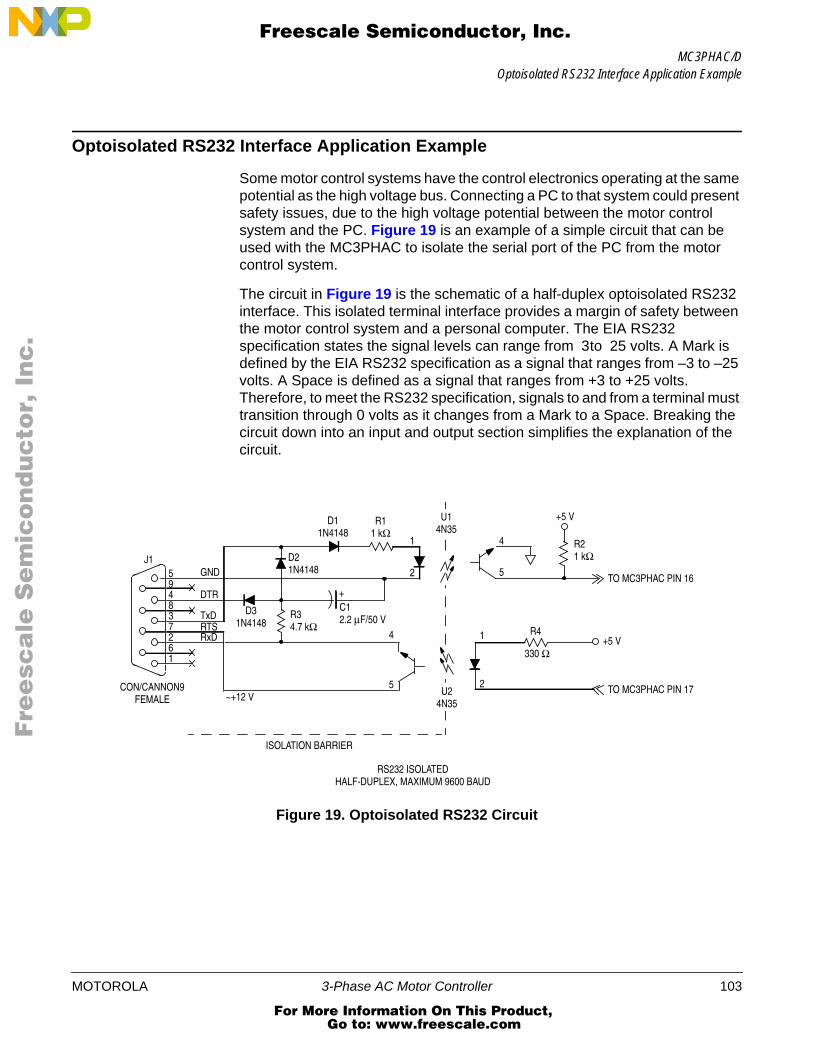
MC3PHAC/DOptoisolated RS232 Interface Application Example
F
ree
sca
le S
em
ico
nd
uc
tor,
I
Freescale Semiconductor, Inc.n
c..
.
Optoisolated RS232 Interface Application Example
Some motor control systems have the control electronics operating at the samepotential as the high voltage bus. Connecting a PC to that system could presentsafety issues, due to the high voltage potential between the motor controlsystem and the PC. Figure 19 is an example of a simple circuit that can beused with the MC3PHAC to isolate the serial port of the PC from the motorcontrol system.
The circuit in Figure 19 is the schematic of a half-duplex optoisolated RS232interface. This isolated terminal interface provides a margin of safety betweenthe motor control system and a personal computer. The EIA RS232specification states the signal levels can range from 3to 25 volts. A Mark isdefined by the EIA RS232 specification as a signal that ranges from –3 to –25volts. A Space is defined as a signal that ranges from +3 to +25 volts.Therefore, to meet the RS232 specification, signals to and from a terminal musttransition through 0 volts as it changes from a Mark to a Space. Breaking thecircuit down into an input and output section simplifies the explanation of thecircuit.
Figure 19. Optoisolated RS232 Circuit
594837261
GND
DTR
TxDRTSRxD
D31N4148
D21N4148
R34.7 kΩ
D11N4148
R11 kΩ
1
2
+C12.2 µF/50 V
~+12 V
4
5
U14N35
U24N35
+5 V
TO MC3PHAC PIN 17
4
5
1
2
R4
330 Ω
+5 V
R21 kΩ
TO MC3PHAC PIN 16
ISOLATION BARRIER
RS232 ISOLATEDHALF-DUPLEX, MAXIMUM 9600 BAUD
J1
CON/CANNON9FEMALE
MOTOROLA 3-Phase AC Motor Controller 103
For More Information On This Product, Go to: www.freescale.com
MC3PHAC/D
F
ree
sca
le S
em
ico
nd
uc
tor,
I
Freescale Semiconductor, Inc.n
c..
.
To send data from a PC to the MC3PHAC, it is necessary to satisfy the serialinput of the MC3PHAC. In the idle condition, the serial input of the MC3PHACmust be at a logic 1. To accomplish that, the transistor in U1 must be turned off.The idle state of the transmit data line (TxD) from the PC serial port is a Mark(–3 to –25 volts). Therefore, the diode in U1 is off and the transistor in U1 is off,yielding a logic 1 to the MC3PHAC’s serial input. When the start bit is sent tothe MC3PHAC from the PC’s serial port, the PC’s TxD transitions from a Markto a Space (+3 to +25 volts), thus forward biasing the diode in U1. Forwardbiasing the diode in D1 turns on the transistor in U1, providing a logic 0 to theserial input of the MC3PHAC. Simply stated, the input half of the circuitprovides input isolation, signal inversion, and level shifting from the PC to theMC3PHAC’s serial port. An RS-232 line receiver, such as an MC1489, servesthe same purpose without the optoisolation function.
To send data from the MC3PHAC to the PC’s serial port input, it is necessaryto satisfy the PC’s receive data (RxD) input requirements. In an idle condition,the RxD input to the PC must be at Mark (–3 to –25 volts). The data terminalready output (DTR) on the PC outputs a Mark when the port is initialized. Therequest to send (RTS) output is set to a Space (+3 to +25 volts) when the PC’sserial port is initialized. Because the interface is half-duplex, the PC’s TxDoutput is also at a Mark, as it is idle. The idle state of the MC3PHAC’s serialport output is a logic 1. The logic 1 out of the MC3PHAC’s serial port output portforces the diode in U2 to be turned off. With the diode in U2 turned off, thetransistor in U2 is also turned off. The junction of D2 and D3 are at a Mark (–3to –25 volts). With the transistor in U2 turned off, the input is pulled to a Markthrough current limiting resistor R3, satisfying the PC’s serial input in an idlecondition. When a start bit is sent from the MC3PHAC’s serial port, it transitionsto a logic 0. That logic 0 turns on the diode in U2, thus turning on the transistorin U2. The conducting transistor in U2 passes the voltage output from the PC’sRTS output, that is now at a Space (+3 to +25 volts), to the PC’s receive data(RxD) input. Capacitor C1 is a bypass capacitor used to stiffen the Mark signal.The output half of the circuit provides output isolation, signal inversion, andlevel shifting from the MC3PHAC’s serial output port to the PC’s serial port. AnRS-232 line driver, such as a MC1488, serves the same purpose without theoptoisolation function.
Mechanical Data
This subsection provides case outline drawings for:
• Plastic 28-pin DIP, Figure 20
• Plastic 28-pin SOIC, Figure 21
• Plastic 32-pin QFP, Figure 22
104 3-Phase AC Motor Controller MOTOROLA
For More Information On This Product, Go to: www.freescale.com
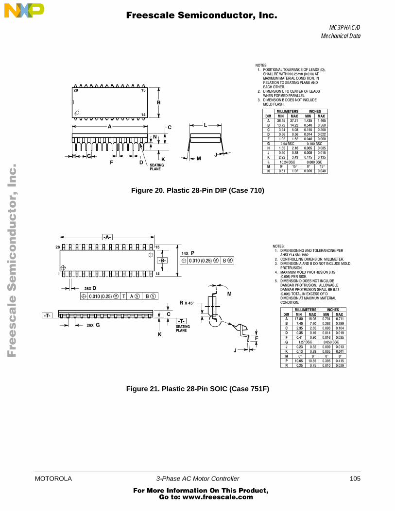
MC3PHAC/DMechanical Data
F
ree
sca
le S
em
ico
nd
uc
tor,
I
Freescale Semiconductor, Inc.n
c..
.
Figure 20. Plastic 28-Pin DIP (Case 710)
Figure 21. Plastic 28-Pin SOIC (Case 751F)
°
°
°
°
!"!#! ! $
! !
! #!
1 14
1528
B
A C
N
K MJ
D
FH G
L
°
°
°
°
!$ $
%! $ ! !! ! # !
# !"!#! ! #
! #
! # ! # " ! !"!#! !
-A-
-B-
1 14
1528
-T- C
! !
M
J
-T-
K
26X G
28X D
14X P
R X 45°
F
!
MOTOROLA 3-Phase AC Motor Controller 105
For More Information On This Product, Go to: www.freescale.com
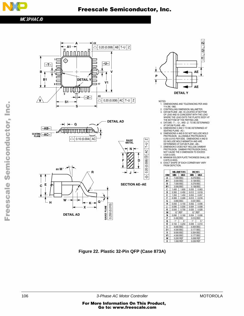
MC3PHAC/D
F
ree
sca
le S
em
ico
nd
uc
tor,
I
Freescale Semiconductor, Inc.n
c..
.
Figure 22. Plastic 32-Pin QFP (Case 873A)
ÉÉÉÉÉÉÉÉ
DETAIL Y
A
S1
VB
1
8
9
17
2532
AE
AE
P
DETAIL Y
BASE
N
J
DF
METAL
SECTION AE–AE
G
SEATINGPLANE
R
Q
WK
X
0.25
0 (0
.010
)
GAU
GE
PLAN
E
EC
H
DETAIL AD
NOTES:1. DIMENSIONING AND TOLERANCING PER ANSI
Y14.5M, 1982.2. CONTROLLING DIMENSION: MILLIMETER.3. DATUM PLANE –AB– IS LOCATED AT BOTTOM
OF LEAD AND IS COINCIDENT WITH THE LEADWHERE THE LEAD EXITS THE PLASTIC BODY ATTHE BOTTOM OF THE PARTING LINE.
4. DATUMS –T–, –U–, AND –Z– TO BE DETERMINEDAT DATUM PLANE –AB–.
5. DIMENSIONS S AND V TO BE DETERMINED ATSEATING PLANE –AC–.
6. DIMENSIONS A AND B DO NOT INCLUDE MOLDPROTRUSION. ALLOWABLE PROTRUSION IS0.250 (0.010) PER SIDE. DIMENSIONS A AND BDO INCLUDE MOLD MISMATCH AND AREDETERMINED AT DATUM PLANE –AB–.
7. DIMENSION D DOES NOT INCLUDE DAMBARPROTRUSION. DAMBAR PROTRUSION SHALLNOT CAUSE THE D DIMENSION TO EXCEED0.520 (0.020).
8. MINIMUM SOLDER PLATE THICKNESS SHALL BE0.0076 (0.0003).
9. EXACT SHAPE OF EACH CORNER MAY VARYFROM DEPICTION.
DIMA
MIN MAX MIN MAXINCHES
7.000 BSC 0.276 BSC
MILLIMETERS
B 7.000 BSC 0.276 BSC
C 1.400 1.600 0.055 0.063D 0.300 0.450 0.012 0.018E 1.350 1.450 0.053 0.057F 0.300 0.400 0.012 0.016G 0.800 BSC 0.031 BSCH 0.050 0.150 0.002 0.006J 0.090 0.200 0.004 0.008K 0.500 0.700 0.020 0.028M 12 REF 12 REFN 0.090 0.160 0.004 0.006P 0.400 BSC 0.016 BSCQ 1 5 1 5 R 0.150 0.250 0.006 0.010
V 9.000 BSC 0.354 BSCV1 4.500 BSC 0.177 BSC
DETAIL AD
A1
B1V1
4X
S
4X
B1 3.500 BSC 0.138 BSC
A1 3.500 BSC 0.138 BSC
S 9.000 BSC 0.354 BSCS1 4.500 BSC 0.177 BSC
W 0.200 REF 0.008 REFX 1.000 REF 0.039 REF
9
–T–
–Z–
–U–
T–U0.20 (0.008) ZAC
T–U0.20 (0.008) ZAB
0.10 (0.004) AC–AC–
–AB–
M8X
–T–,
–U
–, –
Z–
T–U
M0.
20 (0
.008
)Z
AC
106 3-Phase AC Motor Controller MOTOROLA
For More Information On This Product, Go to: www.freescale.com

MC3PHAC/DMechanical Data
F
ree
sca
le S
em
ico
nd
uc
tor,
I
Freescale Semiconductor, Inc.n
c..
.
MOTOROLA 3-Phase AC Motor Controller 107
For More Information On This Product, Go to: www.freescale.com
F
ree
sca
le S
em
ico
nd
uc
tor,
I
Freescale Semiconductor, Inc.n
c..
.
HOW TO REACH US:
USA/EUROPE/LOCATIONS NOT LISTED:
Motorola Literature Distribution;P.O. Box 5405, Denver, Colorado 802171-303-675-2140 or 1-800-441-2447
JAPAN:
Motorola Japan Ltd.; SPS, Technical Information Center,3-20-1, Minami-Azabu Minato-ku, Tokyo 106-8573 Japan81-3-3440-3569
ASIA/PACIFIC:
Motorola Semiconductors H.K. Ltd.;Silicon Harbour Centre, 2 Dai King Street,Tai Po Industrial Estate, Tai Po, N.T., Hong Kong852-26668334
TECHNICAL INFORMATION CENTER:
1-800-521-6274
HOME PAGE:
http://www.motorola.com/semiconductors
Information in this document is provided solely to enable system and software
implementers to use Motorola products. There are no express or implied copyright
licenses granted hereunder to design or fabricate any integrated circuits or
integrated circuits based on the information in this document.
Motorola reserves the right to make changes without further notice to any products
herein. Motorola makes no warranty, representation or guarantee regarding the
suitability of its products for any particular purpose, nor does Motorola assume any
liability arising out of the application or use of any product or circuit, and specifically
disclaims any and all liability, including without limitation consequential or incidental
damages. “Typical” parameters which may be provided in Motorola data sheets
and/or specifications can and do vary in different applications and actual
performance may vary over time. All operating parameters, including “Typicals”
must be validated for each customer application by customer’s technical experts.
Motorola does not convey any license under its patent rights nor the rights of
others. Motorola products are not designed, intended, or authorized for use as
components in systems intended for surgical implant into the body, or other
applications intended to support or sustain life, or for any other application in which
the failure of the Motorola product could create a situation where personal injury or
death may occur. Should Buyer purchase or use Motorola products for any such
unintended or unauthorized application, Buyer shall indemnify and hold Motorola
and its officers, employees, subsidiaries, affiliates, and distributors harmless
against all claims, costs, damages, and expenses, and reasonable attorney fees
arising out of, directly or indirectly, any claim of personal injury or death associated
with such unintended or unauthorized use, even if such claim alleges that Motorola
was negligent regarding the design or manufacture of the part.
Motorola and the Stylized M Logo are registered in the U.S. Patent and TrademarkOffice. digital dna is a trademark of Motorola, Inc. All other product or servicenames are the property of their respective owners. Motorola, Inc. is an EqualOpportunity/Affirmative Action Employer.
© Motorola, Inc. 2002
DRM006/D For More Information On This Product,
Go to: www.freescale.com