drm050, 2.4-ghz wireless optical mouse and multimedia keyboard
TRANSCRIPT

MOTOROLA.COM/SEMICONDUCTORS
M68HC08Microcontrollers
DRM050/DRev. 0, 09/2003
2.4-GHz Wireless
Designer Reference
Optical Mouse and
Manual
Multimedia KeyboardSolution
Fre
esc
ale
Se
mic
on
du
cto
r, I
Freescale Semiconductor, Inc.
For More Information On This Product, Go to: www.freescale.com
nc
...

Fre
esc
ale
Se
mic
on
du
cto
r, I
Freescale Semiconductor, Inc.
For More Information On This Product, Go to: www.freescale.com
nc
...

DRM050 — Rev 0 Designer Reference Manual
MOTOROLA 3
Motorola and the Stylized M Logo are registered trademarks of Motorola, Inc.DigitalDNA is a trademark of Motorola, Inc.This product incorporates SuperFlash® technology licensed from SST. © Motorola, Inc., 2003
2.4-GHz Wireless Optical Mouse and Multimedia Keyboard SolutionDesigner Reference Manual — Rev 0
By: Dennis LuiErnest ChanW.S. WongApplications EngineeringMicrocontroller DivisionHong Kong
To provide the most up-to-date information, the revision of our documents on the World Wide Web will be the most current. Your printed copy may be an earlier revision. To verify you have the latest information available, refer to:
http://motorola.com/semiconductors
The following revision history table summarizes changes contained in this document. For your convenience, the page number designators have been linked to the appropriate location.
Fre
esc
ale
Se
mic
on
du
cto
r, I
Freescale Semiconductor, Inc.
For More Information On This Product, Go to: www.freescale.com
nc
...
Revision History
Designer Reference Manual DRM050 — Rev 0
4 Revision History MOTOROLA
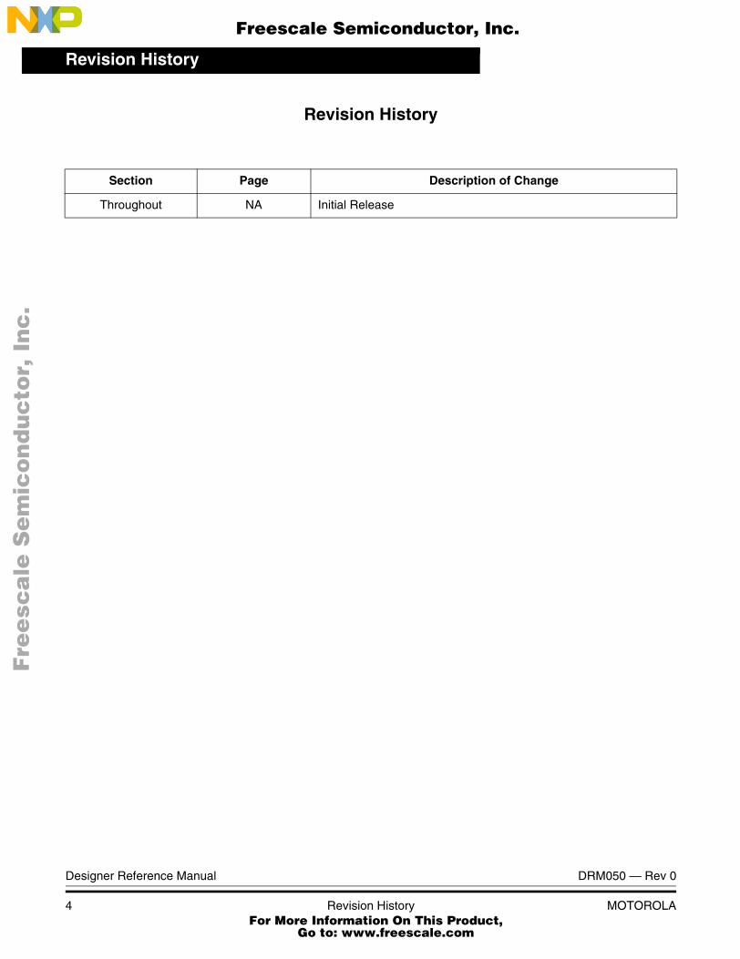
Revision History
Section Page Description of Change
Throughout NA Initial Release
Fre
esc
ale
Se
mic
on
du
cto
r, I
Freescale Semiconductor, Inc.
For More Information On This Product, Go to: www.freescale.com
nc
...

DRM050 — Rev 0 Designer Reference Manual
MOTOROLA 5
Designer Reference Manual — DRM050
Table of Contents
Section 1. System Overview1.1 Introduction . . . . . . . . . . . . . . . . . . . . . . . . . . . . . . . . . . . . . . . . .7
1.2 Features . . . . . . . . . . . . . . . . . . . . . . . . . . . . . . . . . . . . . . . . . . .7
1.3 System Overview . . . . . . . . . . . . . . . . . . . . . . . . . . . . . . . . . . . .8
1.4 Transmit and Receive. . . . . . . . . . . . . . . . . . . . . . . . . . . . . . . . .9
Section 2. RF Front End2.1 Introduction . . . . . . . . . . . . . . . . . . . . . . . . . . . . . . . . . . . . . . . .11
2.2 Functional Description . . . . . . . . . . . . . . . . . . . . . . . . . . . . . . .11
2.3 RF Transceiver Module RFW102 . . . . . . . . . . . . . . . . . . . . . . .12
2.4 Interface IC RFW-D100 . . . . . . . . . . . . . . . . . . . . . . . . . . . . . .14
2.5 Antenna and PCB Specification . . . . . . . . . . . . . . . . . . . . . . . .15
Section 3. Optical Mouse Transmitter3.1 Introduction . . . . . . . . . . . . . . . . . . . . . . . . . . . . . . . . . . . . . . . .17
3.2 System Overview . . . . . . . . . . . . . . . . . . . . . . . . . . . . . . . . . . .173.2.1 Microcontroller JB8. . . . . . . . . . . . . . . . . . . . . . . . . . . . . . . .183.2.2 Optical Mouse Sensor . . . . . . . . . . . . . . . . . . . . . . . . . . . . .183.2.3 RF Transmission . . . . . . . . . . . . . . . . . . . . . . . . . . . . . . . . .193.2.4 DC/DC Converter . . . . . . . . . . . . . . . . . . . . . . . . . . . . . . . . .19
Section 4. Mouse Transmitter Firmware4.1 MAC Layer Protocol . . . . . . . . . . . . . . . . . . . . . . . . . . . . . . . . .21
4.2 Application Firmware Flow . . . . . . . . . . . . . . . . . . . . . . . . . . . .22
4.3 Power Management for the Mouse. . . . . . . . . . . . . . . . . . . . . .23
4.4 Output Buffer Format for the RF Packet . . . . . . . . . . . . . . . . . .24
Fre
esc
ale
Se
mic
on
du
cto
r, I
Freescale Semiconductor, Inc.
For More Information On This Product, Go to: www.freescale.com
nc
...

Designer Reference Manual DRM050 — Rev 0
6 MOTOROLA
Section 5. Multimedia Keyboard Transmitter5.1 Introduction . . . . . . . . . . . . . . . . . . . . . . . . . . . . . . . . . . . . . . . .27
5.2 System Overview . . . . . . . . . . . . . . . . . . . . . . . . . . . . . . . . . . .275.2.1 Microcontroller LK24 . . . . . . . . . . . . . . . . . . . . . . . . . . . . . .285.2.2 RF Transmission . . . . . . . . . . . . . . . . . . . . . . . . . . . . . . . . .285.2.3 DC/DC Converter . . . . . . . . . . . . . . . . . . . . . . . . . . . . . . . . .29
Section 6. Keyboard Transmitter Firmware6.1 Firmware Structure . . . . . . . . . . . . . . . . . . . . . . . . . . . . . . . . . .31
6.2 Output Buffer Format for Keyboard RF Packet. . . . . . . . . . . . .32
Section 7. USB Receiver7.1 Introduction . . . . . . . . . . . . . . . . . . . . . . . . . . . . . . . . . . . . . . . .35
7.2 System Overview . . . . . . . . . . . . . . . . . . . . . . . . . . . . . . . . . . .357.2.1 Microcontroller JB16. . . . . . . . . . . . . . . . . . . . . . . . . . . . . . .367.2.2 RF Transmission . . . . . . . . . . . . . . . . . . . . . . . . . . . . . . . . .367.2.3 Voltage Regulator. . . . . . . . . . . . . . . . . . . . . . . . . . . . . . . . .37
Section 8. Receiver Firmware8.1 Receiver Firmware Structure . . . . . . . . . . . . . . . . . . . . . . . . . .39
8.2 USB Report. . . . . . . . . . . . . . . . . . . . . . . . . . . . . . . . . . . . . . . .418.2.1 Input Report Example. . . . . . . . . . . . . . . . . . . . . . . . . . . . . .43
8.3 Remote Wakeup. . . . . . . . . . . . . . . . . . . . . . . . . . . . . . . . . . . .44
Section 9. Testing and Customization9.1 Testing . . . . . . . . . . . . . . . . . . . . . . . . . . . . . . . . . . . . . . . . . . .45
9.2 Customization . . . . . . . . . . . . . . . . . . . . . . . . . . . . . . . . . . . . . .459.2.1 Hardware . . . . . . . . . . . . . . . . . . . . . . . . . . . . . . . . . . . . . . .459.2.1.1 Optical Mouse Transmitter . . . . . . . . . . . . . . . . . . . . . . . .459.2.1.2 Keyboard Transmitter . . . . . . . . . . . . . . . . . . . . . . . . . . .469.2.1.3 USB Receiver . . . . . . . . . . . . . . . . . . . . . . . . . . . . . . . . .469.2.1.4 RF Circuitry . . . . . . . . . . . . . . . . . . . . . . . . . . . . . . . . . . .469.2.2 Firmware . . . . . . . . . . . . . . . . . . . . . . . . . . . . . . . . . . . . . . .469.2.2.1 Mouse Transmitter . . . . . . . . . . . . . . . . . . . . . . . . . . . . . .469.2.2.2 Keyboard Transmitter . . . . . . . . . . . . . . . . . . . . . . . . . . .469.2.2.3 Receiver . . . . . . . . . . . . . . . . . . . . . . . . . . . . . . . . . . . . . .46
Fre
esc
ale
Se
mic
on
du
cto
r, I
Freescale Semiconductor, Inc.
For More Information On This Product, Go to: www.freescale.com
nc
...

DRM050 — Rev 0 Designer Reference Manual
MOTOROLA System Overview 7
Designer Reference Manual — DRM050
Section 1. System Overview
1.1 Introduction
This manual describes a reference design of a 2.4-GHz Universal Serial Bus Wireless Optical Mouse and Multimedia Keyboard solution by using the MC68HC908JB8, MC68HC908LK24, and MC68HC908JB16.
The whole system consists of a wireless mouse, a wireless keyboard and a USB receiver. The wireless communication link is developed in the worldwide unlicensed Industrial, Scientific, and Medical (ISM) band of 2400–2483 MHz. All hardware schematic diagrams and firmware source codes are available as reference materials.
1.2 Features
• High speed RF link in 2.4-GHz ISM band
• Windows 98, Windows 2000, and Windows XP Compatible1
• USB 2.0 Low Speed Compliance
• 1 Mbps transmission data rate
• 10 to 20 meter communication distance
• RF front end and Media Access Control (MAC) designs are based on RFWaves chipset and protocol
1. Windows 98, Windows 2000 and Windows XP are trademarks of Microsoft Corporation in the U.S. and other countries.
Fre
esc
ale
Se
mic
on
du
cto
r, I
Freescale Semiconductor, Inc.
For More Information On This Product, Go to: www.freescale.com
nc
...

System Overview
Designer Reference Manual DRM050 — Rev 0
8 System Overview MOTOROLA
1.3 System Overview
Figure 1-1. System Overview
The system consists of three functional devices, a wireless optical mouse using the MC68HC908JB8 (hereafter referred as JB8, production version uses the low voltage MC68HC08JT8), a wireless multimedia keyboard using the MC68HC908LK24 (hereafter referred as LK24), and the wireless receiver using the MC68HC908JB16 (hereafter referred as JB16).
The basic structure and functional blocks for each device are similar and consist of a RF transceiver module for half duplex transmission in 2.4-GHz frequency band, a baseband IC for link layer access control and protocol handling. The overall system operation, I/O interface, and power management are controlled by MCU.
Based on the number of I/O pins, voltage operation, and memory size requirements, the JB8 and LK24 are chosen for wireless mouse and
SPI bus
USB
Parallel Address & Data bus
MCU908LK24 /
908JB8
Keyboard/ MouseInterface
RFW-102Module
Antenna
RFW-D100MAC
MCU908JB16
PC HostInterface
RFW-102Module
Antenna
RFW-D100MAC
SPI bus
Parallel Address & Data bus
I/O Detect
Fre
esc
ale
Se
mic
on
du
cto
r, I
Freescale Semiconductor, Inc.
For More Information On This Product, Go to: www.freescale.com
nc
...
System OverviewTransmit and Receive
DRM050 — Rev 0 Designer Reference Manual
MOTOROLA System Overview 9
keyboard designs. The JB16 is specially designed for USB wireless application. It has high processing power and large memory size to handle overall data traffic control for multiple input devices.
1.4 Transmit and Receive
In data transmission, the data generated from the key matrix in a keyboard or displacement detection/button status data in mouse application is detected by MCU and sent to the baseband IC in a parallel format. All kinds of media access, link layout control, and data conversion in serial format are handled by the baseband IC. The final data in serial format is transmitted by the RF module at 2.4 GHz.
In data reception, the data received from RF module is decoded with corresponding protocol, and the serial packet data will be converted into parallel format again in baseband processing. The final data in parallel format will be captured by MCU and sent to the PC host through the USB interface.
Fre
esc
ale
Se
mic
on
du
cto
r, I
Freescale Semiconductor, Inc.
For More Information On This Product, Go to: www.freescale.com
nc
...

System Overview
Designer Reference Manual DRM050 — Rev 0
10 System Overview MOTOROLA
Fre
esc
ale
Se
mic
on
du
cto
r, I
Freescale Semiconductor, Inc.
For More Information On This Product, Go to: www.freescale.com
nc
...

DRM050 — Rev 0 Designer Reference Manual
MOTOROLA RF Front End 11
Designer Reference Manual — DRM050
Section 2. RF Front End
2.1 Introduction
2.4-GHz RF links are designed for wireless communication media for this application. The RF font end of the USB receiver, mouse, and keyboard are the same. The front end is a half duplex direct sequence spread spectrum (DSSS) radio transceiver chipset, intended for use in the world wide unlicensed Industrial, Scientific, and Medical (ISM) band of 2400–2483.5MHz. The front end chipset mainly consist of two parts, the transceiver module RFW102 and the interface IC RFW-D100. CSMA is used as the communication protocol in between the USB receiver, the keyboard, and mouse.
2.2 Functional Description
The complete solution of the RF transceiver consists of an RF transceiver module RFW102 and a link interface IC RFW-D100. The RFW-D100 links the MCU and the transceiver module. When data is being transmitted from the mouse or keyboard, the transmit data from the MCU is passes into the interface IC. In the interface IC, the data will be converted from parallel type to serial type. Also it will be coded with packet address and error checking.
The serial data will then pass to the RF transceiver and ASK modulates into IF frequency 488 MHz. The modulated data will be DSSS spreading and up-converts into 2.4 GHz RF signal for transmission.
When the RF signal is received by the USB receiver, it is down-converted into IF frequency and DSSS de-spreading into ASK IF signal. Then, the ASK IF signal will demodulate into serial data out of the RF transceiver module RFW102.
Fre
esc
ale
Se
mic
on
du
cto
r, I
Freescale Semiconductor, Inc.
For More Information On This Product, Go to: www.freescale.com
nc
...

RF Front End
Designer Reference Manual DRM050 — Rev 0
12 RF Front End MOTOROLA
The received serial data will pass into the interface IC RFW-D100, in which it will be converted to parallel data for the MCU.
2.3 RF Transceiver Module RFW102
The RFW102 transceiver module is a short-range, half-duplex wireless radio transceiver. The transceiver is intended for use in the unlicensed ISM band of 2400–2483.5 MHz.
The transceiver module provides a peak output power of 2 dBm and data rate up to 1Mbps. Power consumption during transmit is extremely low, (21 mA in 1Mbps, 28 mA in 1 kbps), which is directly dependent on the bit transfer rate. During standby mode, the transceiver consumes almost no power and features an extremely short wake up time of 20 ms.
The communication link between the transceivers is a Direct Sequence Spread Spectrum (DSSS) pulse pipe. The modulation scheme is 100%
MCU + GPIOs(JB8/LJ24)
3.3VDC-DC
Battery
Keyboard/
Mouse
RFW-102Module
Antenna
RFW-D100Serial to parallel interface
Parallel Add/Data bus6-24MHz Xtal
Mouse & Keyboard
MCU + GPIOs(JB8/LJ24)
3.3VDC-DC
Battery
Keyboard/
Mouse
RFW-102Module
Antenna
RFW-D100Serial to parallel interface
Parallel Add/Data bus6-24MHz Xtal
Mouse & Keyboard
MCU + GPIOs(JB8/LJ24)
3.3VDC-DC
Battery
3.3VDC-DC
Battery
Keyboard/
Mouse
RFW-102Module
Antenna
RFW-D100Serial to parallel interface
Parallel Add/Data bus6-24MHz Xtal
Mouse & Keyboard
MCU + USB–I/F(JB16)
Power CircuitDC-DC
3.3V
RFW-102Module
Antenna
RFW-D100Serial to parallel interface
Parallel Add/Data bus6-24MHz
USB
+5V
Xtal
USB Dongle
MCU + USB–I/F(JB16)
Power CircuitDC-DC
3.3V
RFW-102Module
Antenna
RFW-D100Serial to parallel interface
Parallel Add/Data bus6-24MHz
USB
+5V
Xtal
USB Dongle
Fre
esc
ale
Se
mic
on
du
cto
r, I
Freescale Semiconductor, Inc.
For More Information On This Product, Go to: www.freescale.com
nc
...

RF Front EndRF Transceiver Module RFW102
DRM050 — Rev 0 Designer Reference Manual
MOTOROLA RF Front End 13
Amplitude Shift Keying (ASK). The spreading modulation scheme is a Bi-Phase modulation where each bit has a 13-bit Barker series.
Below are the key features of the transceiver module:
• 2.4-GHz unlicensed ISM band operation
• 1 Mbps data rate
• Sample 3 line digital interface
• Low power consumption
• +2 dBm typical peak output transmission power
• –80 dBm typical sensitivity
• Typical standby current of 2.6 mA
• Compiles with FCC regulation
• Wide range operating voltage (2.7 V–3.6 V)
• Direct Sequence Spread Spectrum (DSSS) 11 dB processing gain
• Short signal acquisition time (1.2 ms)
The transceiver has a fully digital serial I/O interface providing a simple 3-line interface. Tx/Rx is for controlling of the transceiver work in transmit or receive mode. Act is used for switching the transceiver between working mode and sleep mode. Data IO is the data transfer channel.
The transceiver chipset includes three chips.
• RFW24 — An RFIC performs all of the timing, amplifying, switching, transmitting, and receiving functions.
• RFW488C — A 4-pin SAW correlator, which is used as a direct sequence spread spectrum spreading and de-spreading element.
• RFW488R — A 1-port SAW resonator, which serves as the system oscillation source.
For detailed information on the internal implementation of the transceiver module, please refer to the data sheet about the RFW102 from RFWaves website:
http://www.rfwaves.com
Fre
esc
ale
Se
mic
on
du
cto
r, I
Freescale Semiconductor, Inc.
For More Information On This Product, Go to: www.freescale.com
nc
...

RF Front End
Designer Reference Manual DRM050 — Rev 0
14 RF Front End MOTOROLA
2.4 Interface IC RFW-D100
The RFW-D100 is a complimentary IC to the RFW-102 module. It provides an MCU with a parallel interface to the RFW-102 transceiver module and other features that enable implementing a protocol suitable for wireless communication with a small burden on the MCU.
In HID application, the MCU is in charge of the MAC layer protocol. The RFW-D100 is used to reduce the real-time demands of the MCU handling the MAC protocol. It converts the fast serial input to 8-bit words, which are much easier for 8-bit MCUs to work with. Also, it buffers the input through a 16-byte FIFO, giving the MCU access the RFW-D100 efficiently. Instead of reading one byte per interrupt, the MCU can read up to 16 bytes in each interrupt.
Below are the features of the RFW-D100 interface IC:
• Provides parallel interface with the RFW102 modem
• Serial to parallel conversion of the RFW102 interface
• Input FIFO (RX_FIFO)
• Output FIFO (TX_FIFO)
• Preamble Correlation
• Packet Address Filter
• CRC calculation
• Watchdog Timer driven by internal RC oscillator
• Power saving mode: Idle, Power-down.
• Receiver signal strength indication (RSSI)
For detailed information on the RFW-D100, please refer to the data sheet about the RFW-D100 from the RFWaves website:
http://www.rfwaves.com
Fre
esc
ale
Se
mic
on
du
cto
r, I
Freescale Semiconductor, Inc.
For More Information On This Product, Go to: www.freescale.com
nc
...

RF Front EndAntenna and PCB Specification
DRM050 — Rev 0 Designer Reference Manual
MOTOROLA RF Front End 15
2.5 Antenna and PCB Specification
The antenna interface of the RFWaves module RFW102 is 200 Ω differential. For matching and placement of different antenna, refer to the data sheet of the specific antenna you are using.
The reference antenna of the RFWaves transceiver module RFW102-M used here is a special design printed circuit board differential loop antenna. The purpose of this design is aimed at low cost, small form factor, and high directivity design.
For the dimension and PCB specification of the antenna board, please refer to documents which can be download from RFWaves website: http://www.rfwaves.com
Fre
esc
ale
Se
mic
on
du
cto
r, I
Freescale Semiconductor, Inc.
For More Information On This Product, Go to: www.freescale.com
nc
...

RF Front End
Designer Reference Manual DRM050 — Rev 0
16 RF Front End MOTOROLA
Fre
esc
ale
Se
mic
on
du
cto
r, I
Freescale Semiconductor, Inc.
For More Information On This Product, Go to: www.freescale.com
nc
...

DRM050 — Rev 0 Designer Reference Manual
MOTOROLA Optical Mouse Transmitter 17
Designer Reference Manual — DRM050
Section 3. Optical Mouse Transmitter
3.1 Introduction
The JB8 has 8K Flash memory, 3-MHz bus processing power, 16-bit 2-channel timer module, and appropriate number of I/O pins makes this MCU suited for this 2.4-GHz Wireless Optical Mouse application. The main features of the reference design include:
• 2.4-GHz RF Link
• 1 Mbps data rate
• 800 DPI Resolution
• Smart Power Management
3.2 System Overview
The optical mouse consists of the JB8, the Agilent optical mouse sensor ADNS-2030, the baseband IC and RF Module from RFWaves, and DC/DC converter. Figure 3-1 shows the block diagram of the system.
Fre
esc
ale
Se
mic
on
du
cto
r, I
Freescale Semiconductor, Inc.
For More Information On This Product, Go to: www.freescale.com
nc
...

Optical Mouse Transmitter
Designer Reference Manual DRM050 — Rev 0
18 Optical Mouse Transmitter MOTOROLA
Figure 3-1. Mouse Block Diagram
3.2.1 Microcontroller JB8
The functions of the JB8 are to get the XY displacement from the sensor, detect the Z displacement, check button status, control the baseband IC to sending out data, and perform the overall power management.
Three standard left, middle, and right buttons (and two additional buttons reserved for future development) are implemented.
3.2.2 Optical Mouse Sensor
The AN2030 is a 3-V supply sensor specially design for wireless optical mouse. The communication between the sensor and the JB8 is through Serial Peripheral Interface with clock input at the SCLK pin and bidirection data interface at SDIO pin. The Power Down (PD) pin is used to power down the sensor when it’s not in use.
ADNS-2030
SCLK
SDIO
PDXY_LED
IMAGESENSOR
(16-pin PDIP)
MC68HC908JB8Buttons
PTA0L
M
RPTA1
PTE0
PTA6PTA5
PTA2
Z1
(44-pin QFP)
PTE1
PTE2
DATA BUS
ADDRESS / CTL BUSPTB7-PTB0
PTC7-PTC0
2.4 GHz RF Transceiver
Module
LOOPANTENNA
DGND
L2
R2PTA4
PTA3
Z2
BasebandMAC IC
D100
DC/DC Converters3.3V and 5V
OSC1
OSC2
RST
6MHz30pF 30pF
X1100nF
10M
RFD_INTIRQ
Z-axis Encoder
Fre
esc
ale
Se
mic
on
du
cto
r, I
Freescale Semiconductor, Inc.
For More Information On This Product, Go to: www.freescale.com
nc
...

Optical Mouse TransmitterSystem Overview
DRM050 — Rev 0 Designer Reference Manual
MOTOROLA Optical Mouse Transmitter 19
3.2.3 RF Transmission
The data from the MCU will be transferred to the baseband IC for parallel to serial packet conversion as well as error checking. The encoded data will be passed to the RF module for ASK modulation in IF band and frequency spreading with DSSS scheme. The modulated signal will be further up-converted into 2.4-GHz ISM band for final transmission.
3.2.4 DC/DC Converter
The power supply for a handheld device should be able to keep the DC voltage output at a constant level even though the input battery voltage is continuously dropping down. There are two DC/DC converters; the 3.3-V supply is used for the baseband IC and RF module. The 5-V supply is only used for the JB8, but it would be eliminated in the final product when the low-voltage version JT8 is used.
Fre
esc
ale
Se
mic
on
du
cto
r, I
Freescale Semiconductor, Inc.
For More Information On This Product, Go to: www.freescale.com
nc
...

Optical Mouse Transmitter
Designer Reference Manual DRM050 — Rev 0
20 Optical Mouse Transmitter MOTOROLA
Fre
esc
ale
Se
mic
on
du
cto
r, I
Freescale Semiconductor, Inc.
For More Information On This Product, Go to: www.freescale.com
nc
...

DRM050 — Rev 0 Designer Reference Manual
MOTOROLA Mouse Transmitter Firmware 21
Designer Reference Manual — DRM050
Section 4. Mouse Transmitter Firmware
4.1 MAC Layer Protocol
Each piece of firmware on the mouse, keyboard, or dongle consists of a MAC layer implementing the RFWaves Carrier Sense Multiple Access (CSMA) protocol. In CSMA protocol, every device in the network uses the same physical channel for communication. Each device will first detect whether the channel is being used by others before it initiates its own transmission.
The MAC layer manages the wireless communication between the mouse/keyboard and the dongle through the baseband RFW-D100 IC.
The MAC layer implements two interrupt functions from each of the MCUs. The IRQ and one Timer Channel are used by the MAC.
Interface functions have been built for the application to access the MAC. For example, the application layer can invoke these functions:
• Initiate the MAC layer and the RF hardware
• Initiate transmission of a new packet
• Initiates a packet receiving by the MAC layer
• Check and locate any newly received packet in the MAC buffer
• Sets the MAC and RF hardware to low power mode, or resume from it
The “MACAPI.H” header file in each of the firmware contains more details about these functions and their uses.
Fre
esc
ale
Se
mic
on
du
cto
r, I
Freescale Semiconductor, Inc.
For More Information On This Product, Go to: www.freescale.com
nc
...

Mouse Transmitter Firmware
Designer Reference Manual DRM050 — Rev 0
22 Mouse Transmitter Firmware MOTOROLA
4.2 Application Firmware Flow
Figure 4-1 shows the main application firmware flow of the wireless optical mouse. One of the main challenges in wireless optical mouse design is the power management to minimize the power consumption and maximize the performance.
Figure 4-1. Firmware Structure
MAIN PROGRAM
INIT MAC TO TRANSMIT DATA
POWER MANAGEMENT
INITIATE SENSOR, AND RF HARDWARE
GET XY DISPLACEMENT
GET Z DISPLACEMENT
FROM SENSOR
CHECK BUTTON
FOR EVERY MS
FOR EVERY MS
NEWMOUSE DATA?
Y
N
IRQ ISR
NO
IRQ DRIVEN BY YESPERIODICALWAKEUP SIGNAL?
SERVE THE INTERRUPTEVENT FROM
RFW-D100 BASEBAND CHIP
DISABLE THE PERIODICALWAKEUP FOR MCU TO CHECK
MOVEMENT AND BUTTONS
Fre
esc
ale
Se
mic
on
du
cto
r, I
Freescale Semiconductor, Inc.
For More Information On This Product, Go to: www.freescale.com
nc
...

Mouse Transmitter FirmwarePower Management for the Mouse
DRM050 — Rev 0 Designer Reference Manual
MOTOROLA Mouse Transmitter Firmware 23
The main program continually checks the registers of the sensor to see if any XY movement happened. If any XY movement is detected, it gets the X and Y displacements from the sensor registers, puts them in the FIFO buffer and sets the corresponding flags. For every ms timer tick, it checks the Z movement and the buttons’ status. If new mouse data has been detected, JB8 will initiate the RF data transmission through the baseband RFW-D100 IC.
Apart from serving the interrupt events from the baseband D100 IC during normal operation, IRQ serves as the periodical wakeup signal when JB8 is in sleep mode. The JB8 must check whether there is any new movement or if the buttons’ status changed. IRQ ISR firmware will determine what appropriate actions must be taken.
4.3 Power Management for the Mouse
Figure 4-2. Power Management
Sensor turned on every 25ms, ZLED turned on
for every 700usPOWER SAVING
(STARTUP)
Sensor turned on every 25ms, ZLED turned on
for every 700usPOWER SAVING
(STARTUP)
Sensor fully turned onZLED turned onfor every 700usHIGH CURRENT
Sensor fully turned onZLED turned onfor every 700usHIGH CURRENT
Sensor and ZLED turnedon for every 250ms
SLEEP
xy no movementfor 5s
xyz no movementand
no button for 50s
xy movement
xy movement
z movementor button
Fre
esc
ale
Se
mic
on
du
cto
r, I
Freescale Semiconductor, Inc.
For More Information On This Product, Go to: www.freescale.com
nc
...

Mouse Transmitter Firmware
Designer Reference Manual DRM050 — Rev 0
24 Mouse Transmitter Firmware MOTOROLA
Figure 4-2 shows the flow of the power management. There are three defined stages — Power Saving, High Current, and Sleep stage.
After power up, the mouse is put in Power Saving stage. In this stage, the sensor is only turned on for every 25 ms to see if any XY movement occurred. The Z movement and buttons are sensed for every ms.
If no activity happens in 50 seconds, it enters the Sleep stage. In this stage, the JB8 is put in stop mode and will be woken up every 250 ms to monitor any activity. The RFW-D100 and RFW-D102 IC are in idle mode (not in power down mode). Their power consumption will be reduced because the system CLK to RFW-D100 has been stopped (JB8 and RFW-D100 share the same crystal CLK source).
Any XY movement will cause the mouse to enter the High Current stage. At this stage, the sensor is powered on and XY movement is continually monitored. The Z movement and buttons’ activities are still monitored for every ms. If no XY movement happens in 5 seconds, it then enters Power Saving Stage.
Except for the 1 ms timer tick, all the above mentioned timings can configured by changing their constant values.
4.4 Output Buffer Format for the RF Packet
Users may refer to the RFWaves RFW-D100 IC data sheet for more detail about the RFWaves Packet Structure (Rev 1.3, Appendix B).
Figure 4-3 shows the output buffer format for the mouse RF packet. The contents of this will be transmitted when invoking the transmission function. Users can refer to the “TransmitData” function in “main.c” of the reference firmware as an example.
The first byte is the total size of the buffer data (equal to 11 here). Bytes 2 through 5 are the Network ID which is used to distinguish different RFWaves Networks. Byte 6 is the node ID which is used for identification of different device within the network. The last four bytes are the mouse data.
Fre
esc
ale
Se
mic
on
du
cto
r, I
Freescale Semiconductor, Inc.
For More Information On This Product, Go to: www.freescale.com
nc
...

Mouse Transmitter FirmwareOutput Buffer Format for the RF Packet
DRM050 — Rev 0 Designer Reference Manual
MOTOROLA Mouse Transmitter Firmware 25
The contents of the output buffer will be received by the JB16 dongle and dongle can extract the mouse data and send to the host through USB.
Figure 4-3. Output Buffer Format for the Mouse Packet
Packet Size
Y-DisplacementZ-Displacement
X-DisplacementButton StatusPacket Size
Reserved for SequenceNode ID
Network ID byte4Network ID byte3Network ID byte2Network ID byte1
Packet Size
Y-DisplacementZ-Displacement
X-DisplacementButton StatusPacket Size
Reserved for SequenceNode ID
Network ID byte4Network ID byte3Network ID byte2Network ID byte1
Output Buffer Structure Output Buffer Structure Output Buffer Structure Output Buffer Structure For for Mouse RF PacketFor for Mouse RF PacketFor for Mouse RF PacketFor for Mouse RF Packet
Fre
esc
ale
Se
mic
on
du
cto
r, I
Freescale Semiconductor, Inc.
For More Information On This Product, Go to: www.freescale.com
nc
...

Mouse Transmitter Firmware
Designer Reference Manual DRM050 — Rev 0
26 Mouse Transmitter Firmware MOTOROLA
Fre
esc
ale
Se
mic
on
du
cto
r, I
Freescale Semiconductor, Inc.
For More Information On This Product, Go to: www.freescale.com
nc
...
DRM050 — Rev 0 Designer Reference Manual
MOTOROLA Multimedia Keyboard Transmitter 27
Designer Reference Manual — DRM050
Section 5. Multimedia Keyboard Transmitter
5.1 Introduction
The LK24 has a built-in PLL with a low frequency crystal (32.768 kHz) and is able to operate as fast as 4 MHz bus speed at 3.3 V. It contains enough I/O pins for key matrix scanning. The main features of the keyboard include:
• 2.4-GHz RF Link
• 1 Mbps data rate
• Power management keys (power, wake and sleep) support
• Multimedia keys support
5.2 System Overview
The keyboard transmitter consists of the LK24, the baseband IC and RF Module from RFWaves, and DC/DC converter. Figure 5-1 shows the block diagram of the system.
Fre
esc
ale
Se
mic
on
du
cto
r, I
Freescale Semiconductor, Inc.
For More Information On This Product, Go to: www.freescale.com
nc
...

Multimedia Keyboard Transmitter
Designer Reference Manual DRM050 — Rev 0
28 Multimedia Keyboard Transmitter MOTOROLA
Figure 5-1. Keyboard Block Diagram
5.2.1 Microcontroller LK24
The functions of the LK24 are to scan the key matrix and determine what keys are pressed and released, control the baseband IC to sending out data, and perform the overall system control.
5.2.2 RF Transmission
The data from MCU will be transferred to the baseband IC for parallel to serial packet conversion as well as error checking. The encoded data will be passed to the RF module for ASK modulation in IF band and frequency spreading with DSSS scheme. The modulated signal will be further up-converted into the 2.4-GHz ISM band for final transmission.
2.4 GHz RF Transceiver
Module
LOOPANTENNA
BasebandMAC IC
D100
DC/DC Converter3.3V
OSC1
OSC2
PTF0-7PTC0-7PTB6-7
PTA0-3PTD4-7
[Externalpullup R]
[Externalpullup R]
(80-pin LQFP)
RST
ROW[0:7]
COL[0:17]
Key Matrix(8 rows x 18 columns)
32.768kHz10pF 10pF
X11uF
MC68HC908LK24
PTE7-PTE0
PTA7-PTA4PTD3-PTD0
2M
DATA BUS
ADDRESS / CTL BUS
RFD_INTIRQ
Fre
esc
ale
Se
mic
on
du
cto
r, I
Freescale Semiconductor, Inc.
For More Information On This Product, Go to: www.freescale.com
nc
...

Multimedia Keyboard TransmitterSystem Overview
DRM050 — Rev 0 Designer Reference Manual
MOTOROLA Multimedia Keyboard Transmitter 29
5.2.3 DC/DC Converter
The power supply for a handheld device should be able to keep the DC voltage output at a constant level even though the input battery voltage is continuously dropping down, so a 3.3 V DC/DC converter is designed for the whole system, including the MCU and the baseband IC and RF module.
Fre
esc
ale
Se
mic
on
du
cto
r, I
Freescale Semiconductor, Inc.
For More Information On This Product, Go to: www.freescale.com
nc
...

Multimedia Keyboard Transmitter
Designer Reference Manual DRM050 — Rev 0
30 Multimedia Keyboard Transmitter MOTOROLA
Fre
esc
ale
Se
mic
on
du
cto
r, I
Freescale Semiconductor, Inc.
For More Information On This Product, Go to: www.freescale.com
nc
...

DRM050 — Rev 0 Designer Reference Manual
MOTOROLA Keyboard Transmitter Firmware 31
Designer Reference Manual — DRM050
Section 6. Keyboard Transmitter Firmware
6.1 Firmware Structure
The firmware structure consists of two main parts:
• MAC Layer protocol
• Main Application routine
The MAC layer also implements the RFWaves CSMA protocol. Please refer to the section 4.1 MAC Layer Protocol for a description of this layer.
Figure 6-1 shows the flow of the main program. The main tasks are to detect any key being pressed or released and then send the key code by RF signal through the control of baseband RFW-D100 IC.
If no key is pressed within 10 seconds, LK24 will put the baseband IC into power down mode, LK24 will also enter lower power mode. The MCU will be woken up when any key is pressed.
Fre
esc
ale
Se
mic
on
du
cto
r, I
Freescale Semiconductor, Inc.
For More Information On This Product, Go to: www.freescale.com
nc
...

Keyboard Transmitter Firmware
Designer Reference Manual DRM050 — Rev 0
32 Keyboard Transmitter Firmware MOTOROLA
Figure 6-1. Firmware Flow
6.2 Output Buffer Format for Keyboard RF Packet
Figure 6-2 shows the output buffer format for the keyboard RF packet. It is similar to that of the mouse, except for the last two bytes. Break/Make byte indicates whether the packet represents a Make key
CONVERT SCAN KEY
NO KEY ACTIVITYFOR 10 SECOND?
INITIALIZATION INITIALIZATION
YES
SCAN KEY MATRIX
CONVERT SCAN KEY
NO
YES
ENTERPOWER SAVING MODE
ANY KEY PRESSEDNODETECTED?
WAKE UP DEVICE
VALID KEY PRESSEDDETECTED?
INIT MAC TO TRANSMIT
YES
NO
THE RF PACKET
IRQ ISR
DETERMINE AND SERVETHE INTERRUPT EVENT FROM
RFW-D100 BASEBAND CHIP
Fre
esc
ale
Se
mic
on
du
cto
r, I
Freescale Semiconductor, Inc.
For More Information On This Product, Go to: www.freescale.com
nc
...

Keyboard Transmitter FirmwareOutput Buffer Format for Keyboard RF Packet
DRM050 — Rev 0 Designer Reference Manual
MOTOROLA Keyboard Transmitter Firmware 33
(the key has been pressed) or a Break key (the key has been released). The last byte is the scan code of the key.
Figure 6-2. Packet Format
Packet Size
Scan Code
Break/Make Byte
Packet Size
Reserved for Sequence
Node ID
Network ID byte4
Network ID byte3
Network ID byte2
Network ID byte1
Packet Size
Scan Code
Break/Make Byte
Packet Size
Reserved for Sequence
Node ID
Network ID byte4
Network ID byte3
Network ID byte2
Network ID byte1
Output Buffer Structure Output Buffer Structure Output Buffer Structure Output Buffer Structure For for Keyboard RF PacketFor for Keyboard RF PacketFor for Keyboard RF PacketFor for Keyboard RF Packet
Fre
esc
ale
Se
mic
on
du
cto
r, I
Freescale Semiconductor, Inc.
For More Information On This Product, Go to: www.freescale.com
nc
...

Keyboard Transmitter Firmware
Designer Reference Manual DRM050 — Rev 0
34 Keyboard Transmitter Firmware MOTOROLA
Fre
esc
ale
Se
mic
on
du
cto
r, I
Freescale Semiconductor, Inc.
For More Information On This Product, Go to: www.freescale.com
nc
...

DRM050 — Rev 0 Designer Reference Manual
MOTOROLA USB Receiver 35
Designer Reference Manual — DRM050
Section 7. USB Receiver
7.1 Introduction
The features of JB16 include a Universal Serial Bus (USB) interface, 16K Flash memory, 6-MHz bus clock and two timer modules, which makes this MCU suited for personal computer Human Interface Devices (HID) applications, such a mouse and keyboard. The main features of the receiver include:
• 2.4-GHz RF Link
• 1 Mbps data rate
• Fully USB specification 2.0 low speed compliant
• Windows 98, 2000 and XP compatible
7.2 System Overview
The receiver consists of the JB16, the baseband IC and RF Module from RFWaves and a 3.3-V voltage regulator. Figure 7-1 shows the block diagram of the system.
Fre
esc
ale
Se
mic
on
du
cto
r, I
Freescale Semiconductor, Inc.
For More Information On This Product, Go to: www.freescale.com
nc
...

USB Receiver
Designer Reference Manual DRM050 — Rev 0
36 USB Receiver MOTOROLA
Figure 7-1. USB Receiver Block Diagram
7.2.1 Microcontroller JB16
The functions of the JB16 are to handle the USB transactions, control the baseband IC to receiving input data, and perform the overall system control. The processed data is converted into USB report format and sent to the host.
7.2.2 RF Transmission
The receiving RF signal will be down-converted into IF band for de-spreading with DSSS scheme and ASK demodulation. The demodulated data in serial packet format will be converted back to parallel data and sent to the MCU for USB report generation.
M C68HC908JB16
(28-pin SOIC)
PTE4
PTE3
PTA7-PTA0
PTD5-PTD0PTC1-PTC0
2.4 GHz RF Transceiver
Module
LOOPANTENNA
BasebandM AC IC
D100
3.3V Voltage Regulator
PCHost
DATA BUS
ADDRESS / CTL BUS
RFD_INTIRQ
OSC1
OSC2
RST
12M Hz30pF 30pF
X1100nF
10M
D-
D+
1K5VREG
USB
Fre
esc
ale
Se
mic
on
du
cto
r, I
Freescale Semiconductor, Inc.
For More Information On This Product, Go to: www.freescale.com
nc
...

USB ReceiverSystem Overview
DRM050 — Rev 0 Designer Reference Manual
MOTOROLA USB Receiver 37
7.2.3 Voltage Regulator
The bus power voltage from USB interface is 5 V, so a 3.3-V regulator is added to provide a correct voltage 3.3 V for baseband IC and RF module. The JB16 is specially design for USB application, so external regulated supply input is not necessary.
Fre
esc
ale
Se
mic
on
du
cto
r, I
Freescale Semiconductor, Inc.
For More Information On This Product, Go to: www.freescale.com
nc
...

USB Receiver
Designer Reference Manual DRM050 — Rev 0
38 USB Receiver MOTOROLA
Fre
esc
ale
Se
mic
on
du
cto
r, I
Freescale Semiconductor, Inc.
For More Information On This Product, Go to: www.freescale.com
nc
...

DRM050 — Rev 0 Designer Reference Manual
MOTOROLA Receiver Firmware 39
Designer Reference Manual — DRM050
Section 8. Receiver Firmware
8.1 Receiver Firmware Structure
The firmware consists of three main parts:
• MAC Layer protocol
• Application layer routines
• USB interrupt routine
The MAC layer implements the RFWaves CSMA protocol. Please refer to the section 4.1 MAC Layer Protocol for a description of this layer.
Figure 8-1 shows the flow of the main application program. The USB interrupt routine is not shown here. You may refer to another reference design called USB and PS2 Multimedia Keyboard by using the MC68HC908JB8 for more detail.
The main routine continually checks if there is any valid mouse or keyboard data from the MAC layer. If so, the data will be converted to USB report format and sent to the host via the endpoint 1 and endpoint 2.
IRQ serves for different interrupt events from the RFW-D100 chip when USB is not in suspend mode.The IRQ ISR firmware will determine which interrupt source caused the IRQ. It could be done by checking the IIR register from RFW-D100 Baseband chip and then the corresponding action can be taken by the interrupt service routine. During USB suspend, the periodical wake-up trigger at IRQ can wake up MCU to detect incoming packets and return to the host computer.
Fre
esc
ale
Se
mic
on
du
cto
r, I
Freescale Semiconductor, Inc.
For More Information On This Product, Go to: www.freescale.com
nc
...

Receiver Firmware
Designer Reference Manual DRM050 — Rev 0
40 Receiver Firmware MOTOROLA
Figure 8-1. Firmware Flow
MAIN
RECEIVED MOUSENEWINITIATES MAC LAYER
DEVICE
NEW ENDPOINT 1
NEW ENDPOINT 2
USB IDLE FOR
YES
CONFIGURED ?
YES
CONVERT ANY SCAN KEY TO KEYBOARD REPORT
REPORT ?
REPORT ?
3 MS ?
NO
EP1 TX BUFFERYES
EMPTY ?TX EP1 IN REPORT
YESEP2 TX BUFFER
YES
EMPTY ?TX EP2 IN REPORT
YES RF PACKET
RESUME FROMHOST ?
NO
NO
NO
YES
NO NEW RECEIVED DATA IN MAC LAYER ?
DETECTED OR
CONVERT ANY MOUSE
IRQ ISR
DETERMINE AND SERVE
NO
IRQ DRIVEN BY YES
RECEIVED MOUSENEW
DISABLE THE PERIODICAL
PERIODICALWAKEUP SIGNAL?
ENABLE PERIODIC WAKEUP SIGNAL TO DRIVE IRQ
SUSPEND RF AND MCU
WAKEUP FOR MCU TO CHECKREMOTE WAKEUP PACKET
THE INTERRUPT EVENT FROM D100 BASEBAND CHIP
MAC INITIATEDBEFORE ?
DATA TO MOUSE REPORT
YES
NO
Fre
esc
ale
Se
mic
on
du
cto
r, I
Freescale Semiconductor, Inc.
For More Information On This Product, Go to: www.freescale.com
nc
...

Receiver FirmwareUSB Report
DRM050 — Rev 0 Designer Reference Manual
MOTOROLA Receiver Firmware 41
8.2 USB Report
The mouse and keyboard implement two HID interfaces on endpoint 1 and endpoint 2 in a USB composite-device fashion. HID interface 0 (endpoint 1) implements a standard HID keyboard with identical report and boot protocols. HID interface 1 (endpoint 2) implements multimedia and power management keys and mouse data. This implementation ensures that the keyboard works in BIOS setup and in DOS mode.
Interface 0 will issue 8-byte input reports that are identical to the standard keyboard boot protocol report (see Table 8-1) as documented in the Device Class Definition for Human Interface Device (HID) version 1.1. This interface also allows the host system to send the CAP/NUM/SCROLL lock status to JB16, as specified by the 1-byte output report (see Table 8-2). It can be used to turn on and off the respective LED state indicators if LEDs have been implemented in the hardware. These LEDs are not included in the reference JB16 receiver hardware.
Byte Bit 7 Bit 6 Bit 5 Bit 4 Bit 3 Bit 2 Bit 1 Bit 0
0 RightGUI
RightALT
RightShift
RightControl
LeftGUI
LeftALT
LeftShift
LeftControl
1 Reserved
2 Keyboard Usage ID (Key Code)
3 Keyboard Usage ID (Key Code)
4 Keyboard Usage ID (Key Code)
5 Keyboard Usage ID (Key Code)
6 Keyboard Usage ID (Key Code)
7 Keyboard Usage ID (Key Code)
Table 8-1. Interface 0 Input Report
Fre
esc
ale
Se
mic
on
du
cto
r, I
Freescale Semiconductor, Inc.
For More Information On This Product, Go to: www.freescale.com
nc
...

Receiver Firmware
Designer Reference Manual DRM050 — Rev 0
42 Receiver Firmware MOTOROLA
Interface 1 report contains the power management key report, multimedia key input report, or mouse input report, which is distinguished by a unique Report ID. The power management key uses Report ID number 1 (see Table 8-3); the multimedia key uses Report ID number 2 (see Table 8-4); and the mouse report uses Report ID number 3 (see Table 8-5).
Byte Bit 7 Bit 6 Bit 5 Bit 4 Bit 3 Bit 2 Bit 1 Bit 0
0 ScrollLock
CapsLock
NumLock
Table 8-2. Interface 0 Output Report
Byte Bit 7 Bit 6 Bit 5 Bit 4 Bit 3 Bit 2 Bit 1 Bit 0
0 Report ID = 1
1 Power Wake Sleep
Table 8-3. Interface 1 Power Key Input Report
Byte Bit 7 Bit 6 Bit 5 Bit 4 Bit 3 Bit 2 Bit 1 Bit 0
0 Report ID = 2
1 M7 M6 M5 M4 M3 M2 M1 M0
2 M15 M14 M13 M12 M11 M10 M9 M8
3 M23 M22 M21 M20 M19 M18 M17 M16
4 Reserved for M24 - M31
Table 8-4. Interface 1 Multimedia Key Input Report
Fre
esc
ale
Se
mic
on
du
cto
r, I
Freescale Semiconductor, Inc.
For More Information On This Product, Go to: www.freescale.com
nc
...

Receiver FirmwareUSB Report
DRM050 — Rev 0 Designer Reference Manual
MOTOROLA Receiver Firmware 43
8.2.1 Input Report Example
Table 8-6 shows some input report examples. Report ID is not used in interface 0. The first byte is the modifier byte and is set on bit base. Whenever a modifier key is pressed, the corresponding bit is set to 1. For example, if the Left Control and the character 'A' keys are pressed, the first byte of the report equals $01, the second byte is reserved, the third byte equals $04, and the forth through the eighth bytes equal $00.
Power Management keys are reported through interface 1 with report ID 1. For example, if the Wake key is pressed, the first byte equals $01 (ID = 1), and the second byte equals $02 (corresponding bit equals 1) since Wake key is defined as the bit 2 of the second byte.
Hot keys are reported through interface 1 with reported ID 2. For example, if the hot key 0 and the hot key 17 are pressed, the first byte equals $02 (ID = 2); the second byte equals $01 since hot key 0 is pressed; the third byte equals $00 since hot keys 8 to 16 are not pressed; and the forth byte equals $02 since the hot key 17 is pressed.
Byte Bit 7 Bit 6 Bit 5 Bit 4 Bit 3 Bit 2 Bit 1 Bit 0
0 Report ID = 3
1 Middle button
Right button
Leftbutton
2 X Displacement
3 Y Displacement
4 Z Displacement
Table 8-5. Interface 1 Mouse Input Report
Keys Pressed Endpoint In Report Data
Left Control, ’A’ 1 $01,$00,$04,$00,$00,$00,$00,$00
Left Control, Right Alt, ’A’, ’B’ 1 $41,$00,$04,$05,$00,$00,$00,$00
Wake 2 $01,$02
Hot Key 0 & Hot Key 17 2 $02,$01,$00,$02
Table 8-6. Input Report Examples
Fre
esc
ale
Se
mic
on
du
cto
r, I
Freescale Semiconductor, Inc.
For More Information On This Product, Go to: www.freescale.com
nc
...

Receiver Firmware
Designer Reference Manual DRM050 — Rev 0
44 Receiver Firmware MOTOROLA
8.3 Remote Wakeup
The JB16 receiver supports remote wakeup function that can wake up the host computer during USB suspend.
During suspend, the MCU will be periodically woken up by the IRQ driven by the external RC charging and discharging circuit. The MCU then turns on the RF circuit (both RFW-D100 and RFW-D102) for a short period of time, detect whether a valid mouse or keyboard RF packet arrived for waking up the host. During this short period, the IRQ will serve for RFW-D100 interrupt events again.
If no valid packet has been detected in this period, the receiver will sleep again. The MCU will initiate the charging and discharging cycle again before it enters power saving mode.
The mouse or keyboard can re-transmit an RF packet again if there is no acknowledgment from the JB16 receiver. The maximum number of such re-transmissions can be adjusted through the MAC application interface transmission function.
For the JB16 receiver to be able to detect the incoming packet, some timing parameters needed to be considered.
The first is the small wakeup duration at each IRQ wakeup. For example, if the receiver is sleeping while a packet arrives, the transmitter will send out a second packet because there is no acknowledge from the receiver. If the IRQ wakeup period longer than the interval between the first and next re-transmitted packet, the re-transmitted packet can be detected by the receiver.
Another timing is the interval between two IRQ interrupts. Consider a single key has been pressed on the keyboard. If an IRQ wakeup detection duty in the receiver has just elapsed before the arrival of the first RF keyboard packet, the receiver cannot detect that packet. The next wakeup duty will start at the next IRQ interrupt.
It can be seen that for a smaller number of re-transmission setting in the keyboard, all re-transmission may have taken place before the next wakeup duty start. This means the receiver will fail to detect the pressed key and cannot wake up the host. Therefore, the interval between two IRQ interrupts should be shorter for a relative small re-transmission setting in the transmitter. This time interval can be adjusted by the external RC values, C22, and R45.
Fre
esc
ale
Se
mic
on
du
cto
r, I
Freescale Semiconductor, Inc.
For More Information On This Product, Go to: www.freescale.com
nc
...
DRM050 — Rev 0 Designer Reference Manual
MOTOROLA Testing and Customization 45
Designer Reference Manual — DRM050
Section 9. Testing and Customization
9.1 Testing
The solution was tested under different Windows Operating Systems on several different PCs.
• USB compliance test using Command Verifier version 1.2
• Compatibility tests under Windows 98SE, 2000, and XP
• Compatibility tests of 1AMD 750, Intel 810 and 845 chip set desktops, IBM Thinkpad T23, and Dell Latitude NoteBook C640
9.2 Customization
9.2.1 Hardware
9.2.1.1 Optical Mouse Transmitter
The DC/DC converters/regulators used in this reference design are for reference only, customers can choose any converters/regulators they prefer. The LEDs for the sensor can be connected to the DC/DC converter output or connected to the batteries output. The advantage of connecting to the DC/DC converter output is that the system can work in a lower voltage, but the drawback is higher current consumption. The advantage of connecting to the batteries output is the lower power consumption but the system will not work properly if battery voltage is below 2.5 V.
1. Trademarks are owned by their respective companies.
Fre
esc
ale
Se
mic
on
du
cto
r, I
Freescale Semiconductor, Inc.
For More Information On This Product, Go to: www.freescale.com
nc
...

Testing and Customization
Designer Reference Manual DRM050 — Rev 0
46 Testing and Customization MOTOROLA
9.2.1.2 Keyboard Transmitter
Left the unused pin open.
9.2.1.3 USB Receiver
The diodes connected in series at JB16 VDD can be removed if resistor networks are added in the data/address bus between JB16 and baseband IC as a 5-V to 3.3-V voltage divider.
9.2.1.4 RF Circuitry
The RF transceiver module, the baseband IC, and the CSMA protocol are developed by RFWaves. Please refer to RFWaves website for details and recommendations on RF circuitry customization.
http://www.rfwaves.com
9.2.2 Firmware
9.2.2.1 Mouse Transmitter
• Set the timing parameters for power management.
9.2.2.2 Keyboard Transmitter
• Modify the key matrix tables in “KEY-MAP.ASM” according to customized key matrix.
9.2.2.3 Receiver
• Modify the “KEYMAPTx.H” and USB “KEY-USB.ASM” files according to customized key matrix.
• Change vendor ID, product ID, and product revision number in the device descriptor table in “KBD-MSE.H”.
• Change the report descriptor in “KBS-MSE.H” if necessary.
Fre
esc
ale
Se
mic
on
du
cto
r, I
Freescale Semiconductor, Inc.
For More Information On This Product, Go to: www.freescale.com
nc
...

Fre
esc
ale
Se
mic
on
du
cto
r, I
Freescale Semiconductor, Inc.
For More Information On This Product, Go to: www.freescale.com
nc
...

HOW TO REACH US:
USA/EUROPE/LOCATIONS NOT LISTED:
Motorola Literature Distribution; P.O. Box 5405, Denver, Colorado 80217 1-303-675-2140 or 1-800-441-2447
JAPAN:
Motorola Japan Ltd.; SPS, Technical Information Center, 3-20-1, Minami-Azabu Minato-ku, Tokyo 106-8573 Japan81-3-3440-3569
ASIA/PACIFIC:
Motorola Semiconductors H.K. Ltd.; Silicon Harbour Centre, 2 Dai King Street, Tai Po Industrial Estate, Tai Po, N.T., Hong Kong852-26668334
TECHNICAL INFORMATION CENTER:
1-800-521-6274
HOME PAGE:
http://motorola.com/semiconductors
Information in this document is provided solely to enable system and software
implementers to use Motorola products. There are no express or implied copyright
licenses granted hereunder to design or fabricate any integrated circuits or
integrated circuits based on the information in this document.
Motorola reserves the right to make changes without further notice to any products
herein. Motorola makes no warranty, representation or guarantee regarding the
suitability of its products for any particular purpose, nor does Motorola assume any
liability arising out of the application or use of any product or circuit, and specifically
disclaims any and all liability, including without limitation consequential or incidental
damages. “Typical” parameters which may be provided in Motorola data sheets
and/or specifications can and do vary in different applications and actual
performance may vary over time. All operating parameters, including “Typicals”
must be validated for each customer application by customer’s technical experts.
Motorola does not convey any license under its patent rights nor the rights of
others. Motorola products are not designed, intended, or authorized for use as
components in systems intended for surgical implant into the body, or other
applications intended to support or sustain life, or for any other application in which
the failure of the Motorola product could create a situation where personal injury or
death may occur. Should Buyer purchase or use Motorola products for any such
unintended or unauthorized application, Buyer shall indemnify and hold Motorola
and its officers, employees, subsidiaries, affiliates, and distributors harmless
against all claims, costs, damages, and expenses, and reasonable attorney fees
arising out of, directly or indirectly, any claim of personal injury or death associated
with such unintended or unauthorized use, even if such claim alleges that Motorola
was negligent regarding the design or manufacture of the part.
Motorola and the Stylized M Logo are registered in the U.S. Patent and Trademark Office. digital dna is a trademark of Motorola, Inc. All other product or service names are the property of their respective owners. Motorola, Inc. is an Equal Opportunity/Affirmative Action Employer.
© Motorola, Inc. 2003
DRM050/D
Fre
esc
ale
Se
mic
on
du
cto
r, I
Freescale Semiconductor, Inc.
For More Information On This Product, Go to: www.freescale.com
nc
...