ds89c420 ultra high-speed microcontroller user's guide
TRANSCRIPT
1 of 192 020602
SECTION 1: INTRODUCTION The Dallas Semiconductor DS89C420 is an 8051-compatible microcontroller that provides improved performance and power consumption when compared to the original 8051 version. It retains instruction set and object code compatibility with the 8051, yet performs the same operations in fewer clock cycles. Consequently, greater throughput is possible for the same crystal speed. As an alternative, the DS89C420 can be run at a reduced frequency to save power. The more efficient design allows a much slower crystal speed to get the same results as an original 8051, using much less power. The fundamental innovation of the DS89C420 is the use of only one clock per instruction cycle compared with twelve for the original 8051. This results in up to 12 times improvement in performance over the original 8051 architecture and up to 4 times improvement over other Dallas Semiconductor High-Speed Microcontrollers. The DS89C420 provides several peripherals and features in addition to all of the standard features of an 80C32. These include 16KB of on-chip flash memory, 1KB of on-chip RAM, 4 eight bit I/O ports, three 16-bit timer/counters, two on-chip UARTs, dual data pointers, an on-chip watchdog timer, 5 levels of interrupt priority, and a crystal multiplier. The device provides 256 bytes of RAM for variables and stack. 128 bytes can be reached using direct or indirect addressing and 128 using only indirect addressing. In addition to improved efficiency, the DS89C420 can operate at a maximum clock rate of 33 MHz. Combined with the 12 times performance, this allows for a maximum performance of 33 MIPs. This level of computing power is comparable to many 16-bit processors, but without the added expense and complexity if implementing a 16-bit interface. The DS89C420 incorporates a Power Management Mode which allows the device to dynamically vary the internal clock speed from 1 clock per cycle (default) to 1024 clocks per cycle. Because power consumption is directly proportional to clock speed, the device can reduce its operating frequency during periods of little or no activity. This greatly reduces power consumption. The switch-back feature allows the device to quickly return to highest speed operation upon receipt of an interrupt or serial port activity, allowing the device to respond to external events while in Power Management Mode.
DS89C420 Ultra High-Speed Microcontroller User’s Guide
www.maxim-ic.com
DS89C420 Ultra High-Speed Microcontroller User’s Guide
2 of 192
SECTION 2: ORDERING INFORMATION The DS89C420 family follows the part numbering convention shown below. Note that not all combinations of devices may be currently available. Contact a Maxim / Dallas Semiconductor Sales Office for up to date details.
DS89C420-QCL SPEED: L 33 MHz TEMPERATURE: C 0 °C to 70 °C N -40 °C to 85 °C PACKAGE: M PDIP Q PLCC E Thin Quad Flat Pack (TQFP) OPERATING VOLTAGE: 0 +5V MEMORY TYPE: 9 Flash
DS89C420 Ultra High-Speed Microcontroller User’s Guide
2 of 192
SECTION 3:ARCHITECTURE The DS89C420 Architecture is based on the industry standard 87C52 and executes the standard 8051 instruction set. The core is an accumulator based architecture using internal registers for data storage and peripheral control. This section provides a brief description of each architecture feature. Details concerning the programming model, instruction set, and register description are provided in Section 4. ALU The ALU is responsible for math functions, comparisons, and general decision making in the DS89C420. The ALU is not explicitly used by software. Instruction decoding prepares the ALU automatically and passes it the appropriate data. The ALU primarily uses two special function registers (SFRs) as the source and destination for all operations. These are the Accumulator and B register. The ALU also provides status information in the Program Status Register. The SFRs are described below. SPECIAL FUNCTION REGISTERS All peripherals and operations that are not explicitly controlled by instructions in the DS89C420 are controlled via Special Function Registers (SFRs). All SFRs are described in Section 4. The most commonly used registers that are basic to the architecture are also described below.
Accumulator The Accumulator is the primary register used in the DS89C420. It is a source and destination for many operations involving math, data movement, and decisions. Although it can be bypassed, most high-speed instructions require the use of the Accumulator (A or ACC) as one argument.
B Register The B register is used as the second 8-bit argument in multiply and divide operations. When not used for these purposes, the B register can be used as a general purpose register.
Program Status Word The Program Status Word holds a selection of bit flags that include the Carry Flag, Auxiliary Carry Flag, General Purpose Flag, Register Bank Select, Overflow Flag, and Parity Flag.
Data Pointer(s) The Data Pointers (DPTR and DPTR1) are used to assign a memory address for the MOVX instructions. This address can point to a data memory location, either on- or off-chip, or a memory mapped peripheral. When moving data from one memory area to another or from memory to a memory mapped peripheral, a pointer is needed for both the source and destination. The user can select the active pointer via a dedicated SFR bit (Sel =DPS.0), or can activate an automatic toggling feature for altering the pointer selection (TSL=DPS.5). An additional feature if selected, provides automatic incrementing or decrementing of the current DPTR.
Stack Pointer The Stack Pointer denotes the register location at the top of the Stack, which is the last used value. The user can place the Stack anywhere in the scratchpad RAM by setting the Stack Pointer to the desired location, although the lower bytes are normally used for working registers.
DS89C420 Ultra High-Speed Microcontroller User’s Guide
3 of 192
I/O Ports The DS89C420 offers four 8-bit I/O ports. Each I/O port is represented by an SFR location, and can be written or read. The I/O port has a latch that contains the value written by software. In general, software reads the state of external pins during a read operation.
Timer/Counters
Three 16-bit Timer/Counters are available in the DS89C420. Each timer is contained in two SFR locations that can be written or read by software. The timers are controlled by other SFRs described in Section 4.
UARTs The DS89C420 provides two UARTs which are controlled and accessed by SFRs. Each UART has an address that is used to read and write the UART. The same address is used for both read and write operations, and the read and write operations are distinguished by the instruction. Each UART is controlled by its own SFR control register. SCRATCHPAD REGISTERS (RAM) The High-Speed Core provides 256 bytes of Scratchpad RAM for general purpose data and variable storage. The first 128 bytes are directly available to software. The second 128 are available through indirect addressing discussed below. Selected portions of this RAM have other optional functions.
Stack
The stack is a RAM area that the DS89C420 uses to store return address information during Calls and Interrupts. The user can also place variables on the stack when necessary. The Stack Pointer designates the RAM location that is the top of the stack. Thus, depending on the value of the Stack Pointer, the stack can be located anywhere in the 256 bytes of RAM. A common location would be in the upper 128 bytes of RAM, as these locations are accessible through indirect addressing only.
Working Registers The first thirty-two bytes of the Scratchpad RAM can be used as four banks of eight Working Registers for high speed data movement. Using four banks, software can quickly change context by simply changing to a different bank. In addition to the Accumulator, the Working Registers are commonly used as data source or destination. Some of the Working Registers can also be used as pointers to other RAM locations (indirect addressing).
PROGRAM COUNTER The Program Counter (PC) is a 16-bit value that designates the next program address to be fetched. On-chip hardware automatically increments the PC value to move to the next ROM location.
ADDRESS/DATA BUS The DS89C420 addresses a 64KB program and 64KB data memory area which resides in a combination of internal and external memory. When external memory is accessed, Ports 0 and 2 are used as a multiplexed address and data bus. The DS89C420 supports three external memory bus structures. The non-page mode (traditional 8051) bus structure provides the address MSB on Port 2 and multiplexes Port 0 between address LSB and data. The page mode 1 bus structure uses Port 0 exclusively for data and
DS89C420 Ultra High-Speed Microcontroller User’s Guide
4 of 192
multiplexes Port 2 between address MSB and address LSB. The page mode 2 bus structure uses Port 0 exclusively for address LSB and multiplexes Port 2 between address MSB and data. These addressing modes are detailed later in the User Guide.
WATCHDOG TIMER The Watchdog Timer provides a supervisory function for applications that cannot afford to run out of control. The Watchdog Timer is a programmable free running timer. If allowed to reach the termination of its count, if enabled, the Watchdog will reset the CPU. Software must prevent this by clearing or resetting the Watchdog prior to its time-out.
POWER MONITOR The DS89C420 incorporates a band-gap reference and analog circuitry to monitor the power supply conditions. When VCC begins to drop out of tolerance, the Power Monitor will issue an optional early warning Power-fail interrupt. If power continues to fall, the Power Monitor will invoke a reset condition. This will remain until power returns to normal operating voltage. The Power Monitor also functions on power-up, holding the microcontroller in a reset state until power is stable.
INTERRUPTS The DS89C420 is capable of evaluating thirteen interrupt sources simultaneously. Each interrupt has an associated interrupt vector, flag, priority, and enable. These interrupts can be globally enabled or disabled.
TIMING CONTROL The DS89C420 provides an on-chip oscillator for use with an external crystal. This can be bypassed by injecting a clock source into the XTAL 1 pin. The clock source is used to create machine cycle timing (four clocks), ALE, PSEN , Watchdog, Timer, and serial baud rate timing. In addition, an on-chip ring oscillator can be used to provide an approximately 10 MHz clock source. A frequency multiplier feature is included which can be selected by SFR control to multiply the input clock source by either 2 or 4. This allows lower frequency (and cost) crystals to be used while still allowing internal operation up to the full 33 MHz limit. FLASH MEMORY On-chip program memory is impemented in 16KB of Flash Memory. This can be programmed in system with the standard 5 volt VCC supply under the control of the user software (in-application), or via a serial port (in-system) using a built- in program memory Loader (ROM Loader) or by a standard Flash or EPROM programmer. Full programming details are given in Section 15. The DS89C420 incorporates a Memory Management Unit (MMU) and other hardware to support any of the three programming methods. The MMU controls program and data memory access, and provides sequencing and timing controls for programming of the on-chip program memory. There is also a separate Security Flash block which is used to support a standard three- level lock, a 64-byte encryption array and other Flash options. The full on-chip program memory range can be fetched by the processor automatically. Reset routines and all interrupt vectors are located in the lower 128 bytes of the on-chip program memory area.
DS89C420 Ultra High-Speed Microcontroller User’s Guide
5 of 192
SECTION 4: PROGRAMMING MODEL This section provides a programmer’s overview of the Ultra High-Speed Microcontroller core. It includes information on the memory map, on-chip RAM, Special Function Registers (SFRs), and instruction set. The programming model of the Ultra High-Speed Microcontroller is very similar to that of the industry standard 80C52. The memory map is identical. It uses the same instruction set, with improved instruction timing. Several new SFRs have been added.
MEMORY ORGANIZATION The Ultra High-Speed Microcontroller, like the 8052, uses several distinct memory areas. These areas include Registers, program memory, and data memory. Registers serve to control on-chip peripherals and as RAM. Note that registers (on-chip RAM) are separate from data memory. Registers are divided into three categories including directly addressed on-chip RAM, indirectly addressed on-chip RAM, and Special Function Registers. The program and data memory areas are discussed under Memory Map. The Registers are discussed under Register Map.
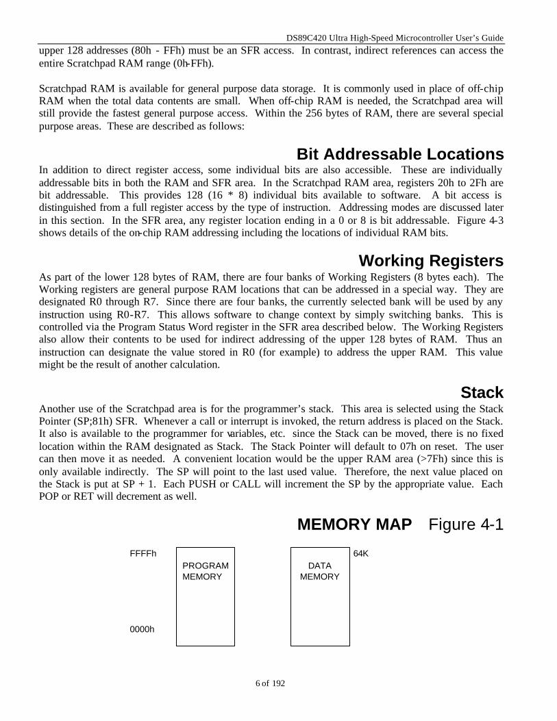
MEMORY MAP The Ultra High-Speed Microcontroller uses a memory addressing scheme that separates program memory from data memory. Each area is 64KB beginning at address 0000h and ending at FFFFh as shown in Figure 4-1. The program and data segments can overlap since they are accessed in different ways. Program memory is fetched by the microcontroller automatically. These addresses are never written by software. In fact, there are no instructions that allow the program area to be written. There is one instruction (MOVC) that is used to explicitly read the program area. This is commonly used to read look-up tables. The data memory area is accessed explicitly using the MOVX instruction. This instruction provides multiple ways of specifying the target address. It is used to access the 64KB of data memory. The address and data range of devices with on-chip program and data memory overlap the 64K memory space. When on-chip memory is enabled, accessing memory in the on-chip range will cause the device to access internal memory. Memory accesses beyond the internal range will be addressed externally via ports 0 and 2. The ROMSIZE feature allows software to dynamically configure the maximum address of on-chip program memory. This allows the device to act as a bootstrap loader for an external Flash or Nonvolatile SRAM. Secondly, this method can also be used to increase the amount of available program memory from 64KB to 80KB without bank switching. For more information on this feature, please consult Section 6. Program and data memory can also be increased beyond the 64KB limit using bank switching techniques. This is described in Application Note 81, Memory Expansion with the High-Speed Microcontroller family.
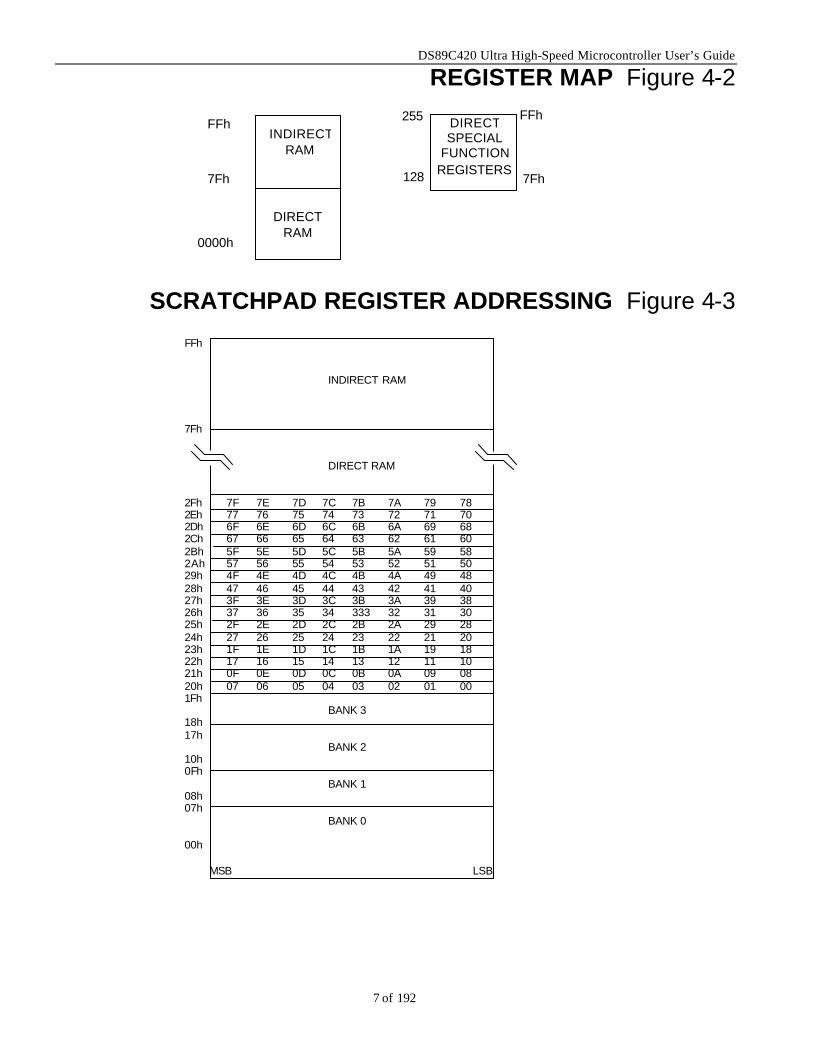
REGISTER MAP The Register Map is illustrated in Figure 4-2. It is entirely separate from the program and data memory areas mentioned above. A separate class of instructions is used to access the registers. There are 256 potential register location values. In practice, the Ultra High-Speed Microcontroller has 256 bytes of Scratchpad RAM and up to 128 Special Function Registers (SFRs). This is possible since the upper 128 Scratchpad RAM locations can only be accessed indirectly. That is, the contents of a Working Register (R0 or R1) or the stack pointer (described below) will designate the RAM location. A direct reference to one of the lower 128 addresses (0-7Fh) will access the Scratchpad RAM. A direct reference to one of the
DS89C420 Ultra High-Speed Microcontroller User’s Guide
6 of 192
upper 128 addresses (80h - FFh) must be an SFR access. In contrast, indirect references can access the entire Scratchpad RAM range (0h-FFh). Scratchpad RAM is available for general purpose data storage. It is commonly used in place of off-chip RAM when the total data contents are small. When off-chip RAM is needed, the Scratchpad area will still provide the fastest general purpose access. Within the 256 bytes of RAM, there are several special purpose areas. These are described as follows:
Bit Addressable Locations In addition to direct register access, some individual bits are also accessible. These are individually addressable bits in both the RAM and SFR area. In the Scratchpad RAM area, registers 20h to 2Fh are bit addressable. This provides 128 (16 * 8) individual bits available to software. A bit access is distinguished from a full register access by the type of instruction. Addressing modes are discussed later in this section. In the SFR area, any register location ending in a 0 or 8 is bit addressable. Figure 4-3 shows details of the on-chip RAM addressing including the locations of individual RAM bits.
Working Registers As part of the lower 128 bytes of RAM, there are four banks of Working Registers (8 bytes each). The Working registers are general purpose RAM locations that can be addressed in a special way. They are designated R0 through R7. Since there are four banks, the currently selected bank will be used by any instruction using R0-R7. This allows software to change context by simply switching banks. This is controlled via the Program Status Word register in the SFR area described below. The Working Registers also allow their contents to be used for indirect addressing of the upper 128 bytes of RAM. Thus an instruction can designate the value stored in R0 (for example) to address the upper RAM. This value might be the result of another calculation.
Stack Another use of the Scratchpad area is for the programmer’s stack. This area is selected using the Stack Pointer (SP;81h) SFR. Whenever a call or interrupt is invoked, the return address is placed on the Stack. It also is available to the programmer for variables, etc. since the Stack can be moved, there is no fixed location within the RAM designated as Stack. The Stack Pointer will default to 07h on reset. The user can then move it as needed. A convenient location would be the upper RAM area (>7Fh) since this is only available indirectly. The SP will point to the last used value. Therefore, the next value placed on the Stack is put at SP + 1. Each PUSH or CALL will increment the SP by the appropriate value. Each POP or RET will decrement as well.
MEMORY MAP Figure 4-1
64K FFFFh
0000h
PROGRAM MEMORY
DATA MEMORY
DS89C420 Ultra High-Speed Microcontroller User’s Guide
7 of 192
REGISTER MAP Figure 4-2
SCRATCHPAD REGISTER ADDRESSING Figure 4-3
FFh
INDIRECT RAM 7Fh
DIRECT RAM 2Fh 7F 7E 7D 7C 7B 7A 79 78 2Eh 77 76 75 74 73 72 71 70 2Dh 6F 6E 6D 6C 6B 6A 69 68 2Ch 67 66 65 64 63 62 61 60 2Bh 5F 5E 5D 5C 5B 5A 59 58 2Ah 57 56 55 54 53 52 51 50 29h 4F 4E 4D 4C 4B 4A 49 48 28h 47 46 45 44 43 42 41 40 27h 3F 3E 3D 3C 3B 3A 39 38 26h 37 36 35 34 333 32 31 30 25h 2F 2E 2D 2C 2B 2A 29 28 24h 27 26 25 24 23 22 21 20 23h 1F 1E 1D 1C 1B 1A 19 18 22h 17 16 15 14 13 12 11 10 21h 0F 0E 0D 0C 0B 0A 09 08 20h 07 06 05 04 03 02 01 00 1Fh
BANK 3 18h 17h
BANK 2 10h 0Fh
BANK 1 08h 07h
BANK 0
00h
255
128
DIRECT SPECIAL
FUNCTION REGISTERS
FFh INDIRECT
RAM
7Fh
0000h
DIRECT RAM
FFh
7Fh
MSB LSB
DS89C420 Ultra High-Speed Microcontroller User’s Guide
8 of 192
ADDRESSING MODES The Ultra High-Speed Microcontroller uses the standard 8051 instruction set which is supported by a wide range of third party assemblers and compilers. Like the 8051, the Ultra High-Speed Microcontroller uses three memory areas. These are program memory, data memory, and Registers. The program and data areas are 64KB each. They extend from 0000h to FFFFh. The register areas are located between 00h and FFh, but do not overlap with the program and data segments. This is because the Ultra High-Speed Microcontroller uses different modes of addressing to reach each memory segment. These modes are described below. Program memory is the area from which all instructions are fetched. It is inherently read only. This is because the 8051 instruction set provides no instructions that write to this area. Read/write access is for data memory and Registers only. No special action is required to fetch from program memory. Each instruction fetch will be performed automatically by the on-chip CPU. In versions that contain on chip memory, the hardware will decide whether the fetch is on-chip or off-chip based on the address. Explicit addressing modes are needed for the data memory and register areas. These modes determine which register area is accessed or if off-chip data memory is used. The Ultra High-Speed Microcontroller supports eight addressing modes. They are:
Register Addressing Direct Addressing Register Indirect Addressing Immediate Addressing Register Indirect Addressing with Displacement Relative Addressing Page Addressing Extended Addressing
Five of the eight are used to address operands. The remainder are used for program control and branching. When writing assembly language instructions that use arguments, the convention is destination, source. Each mode of addressing is summarized below. Note that many instructions (such as ADD) have multiple addressing modes available.
DS89C420 Ultra High-Speed Microcontroller User’s Guide
9 of 192
Register Addressing Register Addressing is used for operands that are located in one of the eight Working Registers (R7-R0). The eight Working Registers can be located in one of four Working Register banks found in the lower 32 bytes of Scratchpad RAM, as determined by the current register bank select bits. A register bank is selected using two bits in the Program Status Word (PSW;D0h). This addressing mode is powerful, since it uses the active bank without knowing which bank is selected. Thus one instruction can have multiple uses by simply switching banks. Register Addressing is also a high-speed instruction, requiring only one machine cycle. Two examples of Register Addressing are provided below.
ADD A, R4 ;Add register R4 to Accumulator INC R2 ;Increment the value in register R2
In the first case, the value in R4 is the source of the operation. In the later, R2 is the destination. These instructions do not consider the absolute address of the register. They will act on whichever bank has been selected. Any Working Register may also be accessed by Direct Addressing, described below. To do this, the absolute address must be specified.
Direct Addressing Direct Addressing is the mode used to access the entire lower 128 bytes of Scratchpad RAM and the SFR area. It is commonly used to move the value in one register to another. Two examples are shown below.
MOV 72h, 74h ;Move the value in register 74 to ;register 72.
MOV 90h, 20h ;Move the value in register 20 to ;the SFR at 90h (Port 1)
Note that there is no instruction difference between a RAM access and an SFR access. The SFRs are simply register locations above 7Fh. Direct Addressing also extends to bit addressing. There is a group of instructions that explicitly use bits. The address information provided to such an instruction is the bit location, rather than the register address. Registers between 20h and 2Fh contain bits that are individually addressable. SFRs that end in 0 or 8 are bit addressable. An example of Direct Bit Addressing is as follows.
SETB 00h ;Set bit 00 in the RAM. This is the ;LSb of the register at address 20h ;as shown earlier in this section.
MOV C, 0B7h ;Move the contents of bit B7 to the
;Carry flag. Bit B7 is the MSb of ;register B0 (Port 3).
DS89C420 Ultra High-Speed Microcontroller User’s Guide
10 of 192
Register Indirect Addressing This mode is used to access the Scratchpad RAM locations above 7Fh. It can also be used to reach the lower RAM (0h - 7Fh) if needed. The address is supplied by the contents of the Working Register specified in the instruction. Thus one instruction can be used to reach many values by altering the contents of the designated Working Register. Note that in general, only R0 and R1 can be used as pointers. An example of Register Indirect Addressing is as follows.
ANL A, @R0 ;Logical AND the Accumulator ;with the contents of the register ;pointed to by the value stored in R0.
This mode is also used for Stack manipulation. This is because all Stack references are directed by the value in the Stack Pointer register. The Push and Pop instructions use this method of addressing. An example is as follows.
PUSH A ;Saves the contents of the ;accumulator on the stack.
Register Indirect Addressing is used for all off-chip data memory accesses. These involve the MOVX instruction. The pointer registers can be R0, R1, DPTR0 and DPTR1. Both R0 and R1 reside in the Working Register area of the Scratchpad RAM. They can be used to reference a 256 byte area of off-chip data memory. When using this type of addressing, the upper address byte is supplied by the value in the Port 2 latch. This value must be selected by software prior to the MOVX instruction. An example is as follows.
MOVX @R0, A ;Write the value in the accumulator ;to the address pointed to by R0 in ;the page pointed to by P2.
The 16-bit Data pointers (DPTRs) can be used as an absolute off-chip reference. This gives access to the entire 64KB data memory map. An example is as fo llows.
MOVX @DPTR, A ;Write the value in the accumulator ;to the address referenced by the ;selected data pointer.
Immediate Addressing Immediate Addressing is used when one of the operands is predetermined and coded into the software. This mode is commonly used to initialize SFRs and to mask particular bits without affecting others. An example is as follows.
ORL A, #40h ;Logical OR the Accumulator with 40h.
DS89C420 Ultra High-Speed Microcontroller User’s Guide
11 of 192
Register Indirect with Displacement Register Indirect Addressing with Displacement is used to access data in lookup tables in program memory space. The location is created using a base address with an index. The base address can be either the PC or the DPTR. The index is the accumulator. The result is stored in the accumulator. An example is as follows.
MOVC A, @A +DPTR ;Load the accumulator with the contents of program memory ;pointed to by the contents of the DPTR plus the value in ;the accumulator.
Relative Addressing Relative Addressing is used to determine a destination address for Conditional branch. Each of these instructions includes an 8-bit value that contains a two’s complement address offset (–127 to +128) which is added to the PC to determine the destination address. This destination is branched to when the tested condition is true. The PC points to the program memory location immediately following the branch instruction when the offset is added. If the tested condition is not true, the next instruction is performed. An example is as follows.
JZ $–20 ;Branch to the location (PC+2)–20 ;if the contents of the accumulator = 0.
Page Addressing Page Addressing is used by the Branching instructions to specify a destination address within the same 2KB block as the next contiguous instruction. The full 16-bit address is calculated by taking the five highest order bits for the next instruction (PC+2) and concatenating them with the lowest order 11 bit field contained in the current instruction. An example is as follows.
0870h ACALL 100h ;Call to the subroutine at address 100h plus the ;current page address.
In this example, the current page address is 800h, so the destination address is 900h.
Extended Addressing Extended Addressing is used by the Branching instructions to specify a 16-bit destination address within the 64KB address space. The destination address is fixed in software as an absolute value. An example is as follows.
LJMP 0F732h ;Jump to address 0F732h.
DS89C420 Ultra High-Speed Microcontroller User’s Guide
12 of 192
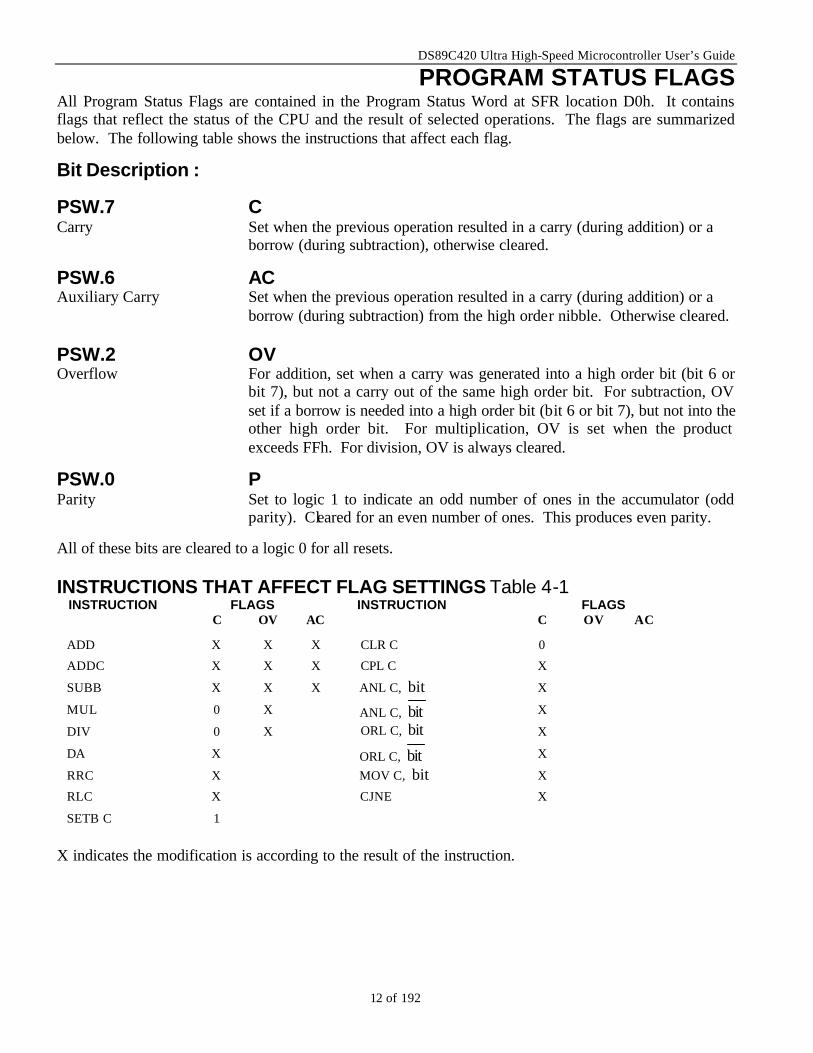
PROGRAM STATUS FLAGS All Program Status Flags are contained in the Program Status Word at SFR location D0h. It contains flags that reflect the status of the CPU and the result of selected operations. The flags are summarized below. The following table shows the instructions that affect each flag.
Bit Description :
PSW.7 C Carry Set when the previous operation resulted in a carry (during addition) or a
borrow (during subtraction), otherwise cleared.
PSW.6 AC Auxiliary Carry Set when the previous operation resulted in a carry (during addition) or a
borrow (during subtraction) from the high order nibble. Otherwise cleared.
PSW.2 OV Overflow For addition, set when a carry was generated into a high order bit (bit 6 or
bit 7), but not a carry out of the same high order bit. For subtraction, OV set if a borrow is needed into a high order bit (bit 6 or bit 7), but not into the other high order bit. For multiplication, OV is set when the product exceeds FFh. For division, OV is always cleared.
PSW.0 P Parity Set to logic 1 to indicate an odd number of ones in the accumulator (odd
parity). Cleared for an even number of ones. This produces even parity.
All of these bits are cleared to a logic 0 for all resets. INSTRUCTIONS THAT AFFECT FLAG SETTINGS Table 4-1 INSTRUCTION FLAGS INSTRUCTION FLAGS
C OV AC C OV AC
ADD X X X CLR C 0
ADDC X X X CPL C X
SUBB X X X ANL C, bit X
MUL 0 X ANL C, bit X
DIV 0 X ORL C, bit X
DA X ORL C, bit X
RRC X MOV C, bit X
RLC X CJNE X
SETB C 1
X indicates the modification is according to the result of the instruction.
DS89C420 Ultra High-Speed Microcontroller User’s Guide
13 of 192
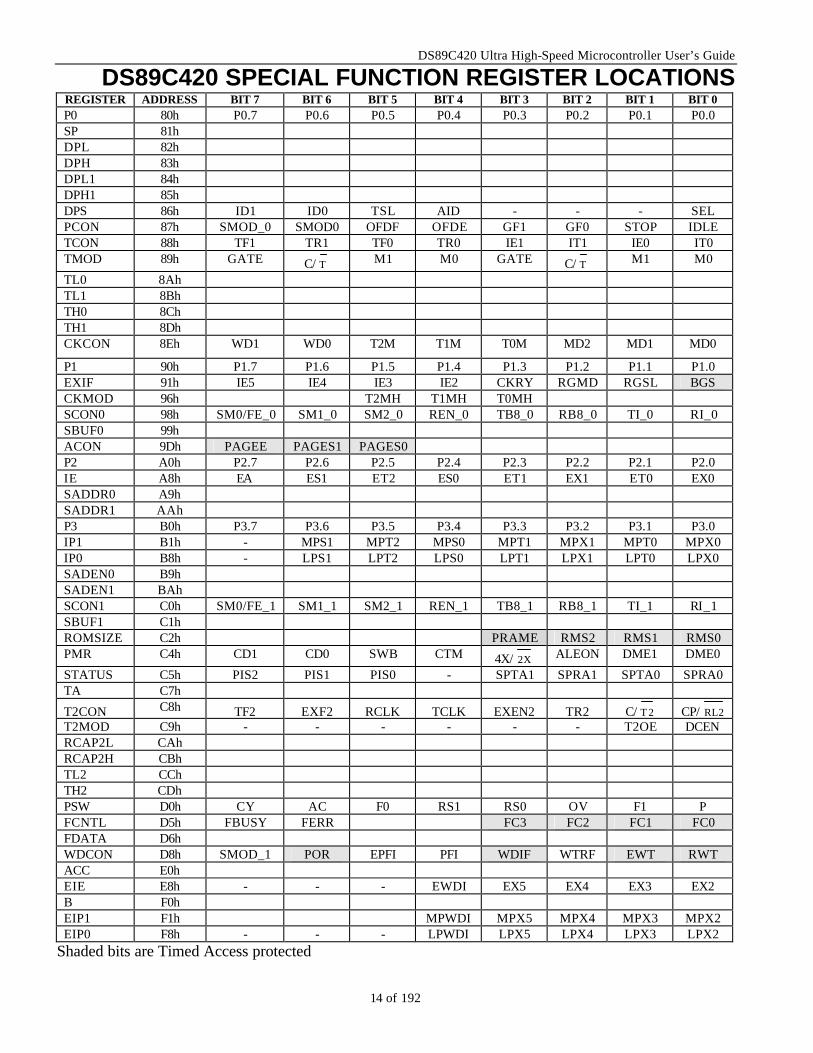
SPECIAL FUNCTION REGISTERS The DS89C420, like the 8051, uses Special Function Registers (SFRs) to control peripherals and modes. In many cases, an SFR will control individual functions or report status on individual functions. The SFRs reside in register locations 80h-FFh and are reached using direct addressing. SFRs that end in 0 or 8 are bit addressable. All standard SFR locations from the original 8051 are duplicated in the DS89C420, with several additions. Tables are provided to illustrate the locations of the SFRs for the DS89C420 device and the default reset conditions of all SFR bits. Detailed descriptions of each Special Function Register follow.
DS89C420 Ultra High-Speed Microcontroller User’s Guide
14 of 192
DS89C420 SPECIAL FUNCTION REGISTER LOCATIONS REGISTER ADDRESS BIT 7 BIT 6 BIT 5 BIT 4 BIT 3 BIT 2 BIT 1 BIT 0 P0 80h P0.7 P0.6 P0.5 P0.4 P0.3 P0.2 P0.1 P0.0 SP 81h DPL 82h DPH 83h DPL1 84h DPH1 85h DPS 86h ID1 ID0 TSL AID - - - SEL PCON 87h SMOD_0 SMOD0 OFDF OFDE GF1 GF0 STOP IDLE TCON 88h TF1 TR1 TF0 TR0 IE1 IT1 IE0 IT0 TMOD 89h GATE C/ T M1 M0 GATE C/ T M1 M0
TL0 8Ah TL1 8Bh TH0 8Ch TH1 8Dh CKCON 8Eh WD1 WD0 T2M T1M T0M MD2 MD1 MD0
P1 90h P1.7 P1.6 P1.5 P1.4 P1.3 P1.2 P1.1 P1.0 EXIF 91h IE5 IE4 IE3 IE2 CKRY RGMD RGSL BGS CKMOD 96h T2MH T1MH T0MH SCON0 98h SM0/FE_0 SM1_0 SM2_0 REN_0 TB8_0 RB8_0 TI_0 RI_0 SBUF0 99h ACON 9Dh PAGEE PAGES1 PAGES0 P2 A0h P2.7 P2.6 P2.5 P2.4 P2.3 P2.2 P2.1 P2.0 IE A8h EA ES1 ET2 ES0 ET1 EX1 ET0 EX0 SADDR0 A9h SADDR1 AAh P3 B0h P3.7 P3.6 P3.5 P3.4 P3.3 P3.2 P3.1 P3.0 IP1 B1h - MPS1 MPT2 MPS0 MPT1 MPX1 MPT0 MPX0 IP0 B8h - LPS1 LPT2 LPS0 LPT1 LPX1 LPT0 LPX0 SADEN0 B9h SADEN1 BAh SCON1 C0h SM0/FE_1 SM1_1 SM2_1 REN_1 TB8_1 RB8_1 TI_1 RI_1 SBUF1 C1h ROMSIZE C2h PRAME RMS2 RMS1 RMS0 PMR C4h CD1 CD0 SWB CTM 4X/ 2X ALEON DME1 DME0
STATUS C5h PIS2 PIS1 PIS0 - SPTA1 SPRA1 SPTA0 SPRA0 TA C7h
T2CON C8h TF2 EXF2 RCLK TCLK EXEN2 TR2 C/ T 2 CP/ RL2 T2MOD C9h - - - - - - T2OE DCEN RCAP2L CAh RCAP2H CBh TL2 CCh TH2 CDh PSW D0h CY AC F0 RS1 RS0 OV F1 P FCNTL D5h FBUSY FERR FC3 FC2 FC1 FC0 FDATA D6h WDCON D8h SMOD_1 POR EPFI PFI WDIF WTRF EWT RWT ACC E0h EIE E8h - - - EWDI EX5 EX4 EX3 EX2 B F0h EIP1 F1h MPWDI MPX5 MPX4 MPX3 MPX2 EIP0 F8h - - - LPWDI LPX5 LPX4 LPX3 LPX2
Shaded bits are Timed Access protected

DS89C420 Ultra High-Speed Microcontroller User’s Guide
15 of 192
DS89C420 SPECIAL FUNCTION REGISTER RESET VALUES
REGISTER ADDRESS BIT 7 BIT 6 BIT 5 BIT 4 BIT 3 BIT 2 BIT 1 BIT 0 P0 80h 1 1 1 1 1 1 1 1 SP 81h 0 0 0 0 0 1 1 1 DPL 82h 0 0 0 0 0 0 0 0 DPH 83h 0 0 0 0 0 0 0 0 DPL1 84h 0 0 0 0 0 0 0 0 DPH1 85h 0 0 0 0 0 0 0 0 DPS 86h 0 0 0 0 0 1 0 0 PCON 87h 0 0 Special Special 0 0 0 0 TCON 88h 0 0 0 0 0 0 0 0 TMOD 89h 0 0 0 0 0 0 0 0 TL0 8Ah 0 0 0 0 0 0 0 0 TL1 8Bh 0 0 0 0 0 0 0 0 TH0 8Ch 0 0 0 0 0 0 0 0 TH1 8Dh 0 0 0 0 0 0 0 0 CKCON 8Eh 0 0 0 0 0 0 0 1 P1 90h 1 1 1 1 1 1 1 1 EXIF 91h 0 0 0 0 Special Special Special 0 CKMOD 96h 1 1 0 0 0 1 1 1 SCON0 98h 0 0 0 0 0 0 0 0 SBUF0 99h 0 0 0 0 0 0 0 0 ACON 9Dh 0 0 0 1 1 1 1 1 P2 A0h 1 1 1 1 1 1 1 1 IE A8h 0 0 0 0 0 0 0 0 SADDR0 A9h 0 0 0 0 0 0 0 0 SADDR1 AAh 0 0 0 0 0 0 0 0 P3 B0h 1 1 1 1 1 1 1 1 IP1 B1h 1 0 0 0 0 0 0 0 IP0 B8h 1 0 0 0 0 0 0 0 SADEN0 B9h 0 0 0 0 0 0 0 0 SADEN1 BAh 0 0 0 0 0 0 0 0 SCON1 C0h 0 0 0 0 0 0 0 0 SBUF1 C1h 0 0 0 0 0 0 0 0 ROMSIZE C2h 1 1 1 1 0 1 0 1 PMR C4h 1 0 0 0 0 0 0 0 STATUS C5h 0 0 0 1 0 0 0 0 TA C7h 1 1 1 1 1 1 1 1 T2CON C8h 0 0 0 0 0 0 0 0 T2MOD C9h 1 1 1 1 1 1 0 0 RCAP2L CAh 0 0 0 0 0 0 0 0 RCAP2H CBh 0 0 0 0 0 0 0 0 TL2 CCh 0 0 0 0 0 0 0 0 TH2 CDh 0 0 0 0 0 0 0 0 PSW D0h 0 0 0 0 0 0 0 0 FCNTL D5h 1 0 1 1 0 0 0 0 FDATA D6h 0 0 0 0 0 0 0 0 WDCON D8h 0 Special 0 Special 0 Special Special 0 ACC E0h 0 0 0 0 0 0 0 0 EIE E8h 1 1 1 0 0 0 0 0 B F0h 0 0 0 0 0 0 0 0 EIP1 F1h 1 1 1 0 0 0 0 0 EIP0 F8h 1 1 1 0 0 0 0 0
DS89C420 Ultra High-Speed Microcontroller User’s Guide
16 of 192
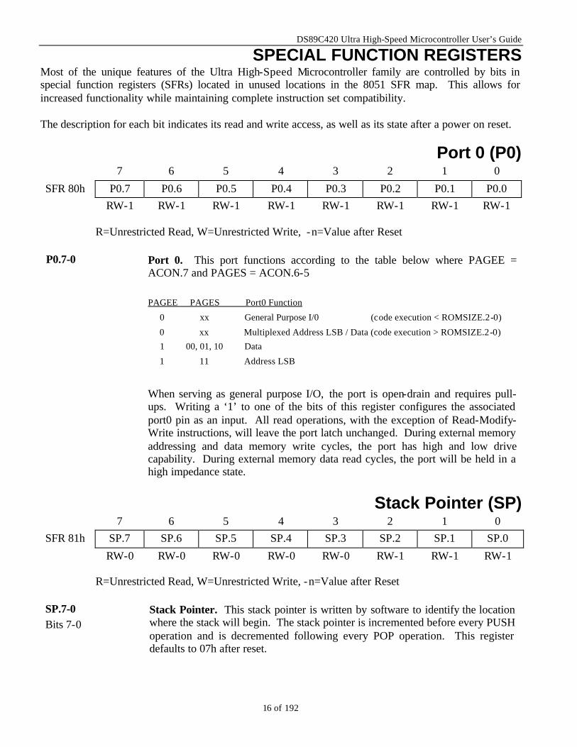
SPECIAL FUNCTION REGISTERS Most of the unique features of the Ultra High-Speed Microcontroller family are controlled by bits in special function registers (SFRs) located in unused locations in the 8051 SFR map. This allows for increased functionality while maintaining complete instruction set compatibility. The description for each bit indicates its read and write access, as well as its state after a power on reset.
Port 0 (P0) 7 6 5 4 3 2 1 0
SFR 80h P0.7 P0.6 P0.5 P0.4 P0.3 P0.2 P0.1 P0.0 RW-1 RW-1 RW-1 RW-1 RW-1 RW-1 RW-1 RW-1
R=Unrestricted Read, W=Unrestricted Write, -n=Value after Reset
P0.7-0 Port 0. This port functions according to the table below where PAGEE = ACON.7 and PAGES = ACON.6-5
PAGEE PAGES Port0 Function
0 xx General Purpose I/0 (code execution < ROMSIZE.2-0)
0 xx Multiplexed Address LSB / Data (code execution > ROMSIZE.2-0)
1 00, 01, 10 Data
1 11 Address LSB
When serving as general purpose I/O, the port is open-drain and requires pull-ups. Writing a ‘1’ to one of the bits of this register configures the associated port0 pin as an input. All read operations, with the exception of Read-Modify-Write instructions, will leave the port latch unchanged. During external memory addressing and data memory write cycles, the port has high and low drive capability. During external memory data read cycles, the port will be held in a high impedance state.
Stack Pointer (SP) 7 6 5 4 3 2 1 0
SFR 81h SP.7 SP.6 SP.5 SP.4 SP.3 SP.2 SP.1 SP.0 RW-0 RW-0 RW-0 RW-0 RW-0 RW-1 RW-1 RW-1
R=Unrestricted Read, W=Unrestricted Write, -n=Value after Reset
SP.7-0 Bits 7-0
Stack Pointer. This stack pointer is written by software to identify the location where the stack will begin. The stack pointer is incremented before every PUSH operation and is decremented following every POP operation. This register defaults to 07h after reset.
DS89C420 Ultra High-Speed Microcontroller User’s Guide
17 of 192
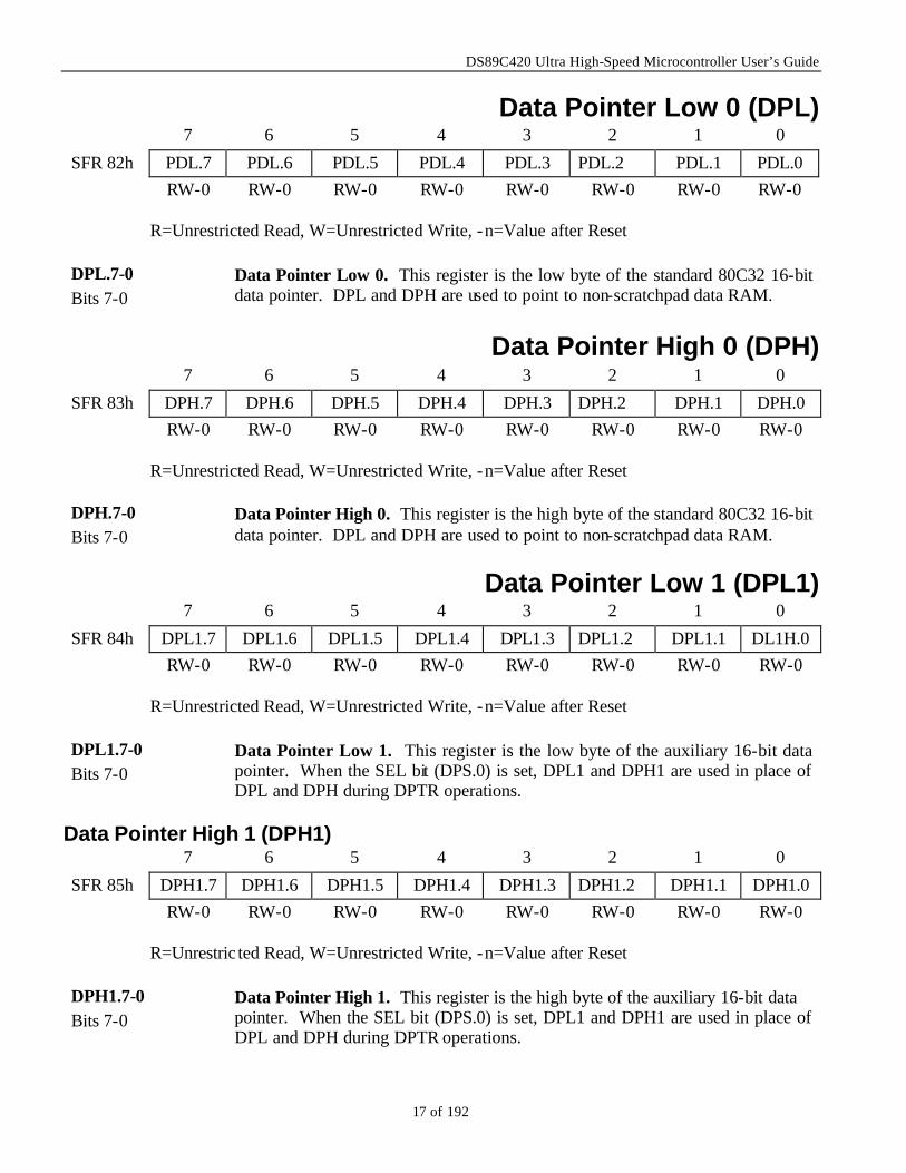
Data Pointer Low 0 (DPL) 7 6 5 4 3 2 1 0
SFR 82h PDL.7 PDL.6 PDL.5 PDL.4 PDL.3 PDL.2 PDL.1 PDL.0 RW-0 RW-0 RW-0 RW-0 RW-0 RW-0 RW-0 RW-0
R=Unrestricted Read, W=Unrestricted Write, -n=Value after Reset
DPL.7-0 Bits 7-0
Data Pointer Low 0. This register is the low byte of the standard 80C32 16-bit data pointer. DPL and DPH are used to point to non-scratchpad data RAM.
Data Pointer High 0 (DPH) 7 6 5 4 3 2 1 0
SFR 83h DPH.7 DPH.6 DPH.5 DPH.4 DPH.3 DPH.2 DPH.1 DPH.0 RW-0 RW-0 RW-0 RW-0 RW-0 RW-0 RW-0 RW-0
R=Unrestricted Read, W=Unrestricted Write, -n=Value after Reset
DPH.7-0 Bits 7-0
Data Pointer High 0. This register is the high byte of the standard 80C32 16-bit data pointer. DPL and DPH are used to point to non-scratchpad data RAM.
Data Pointer Low 1 (DPL1) 7 6 5 4 3 2 1 0
SFR 84h DPL1.7 DPL1.6 DPL1.5 DPL1.4 DPL1.3 DPL1.2 DPL1.1 DL1H.0 RW-0 RW-0 RW-0 RW-0 RW-0 RW-0 RW-0 RW-0
R=Unrestricted Read, W=Unrestricted Write, -n=Value after Reset
DPL1.7-0 Bits 7-0
Data Pointer Low 1. This register is the low byte of the auxiliary 16-bit data pointer. When the SEL bit (DPS.0) is set, DPL1 and DPH1 are used in place of DPL and DPH during DPTR operations.
Data Pointer High 1 (DPH1) 7 6 5 4 3 2 1 0
SFR 85h DPH1.7 DPH1.6 DPH1.5 DPH1.4 DPH1.3 DPH1.2 DPH1.1 DPH1.0 RW-0 RW-0 RW-0 RW-0 RW-0 RW-0 RW-0 RW-0
R=Unrestric ted Read, W=Unrestricted Write, -n=Value after Reset
DPH1.7-0 Bits 7-0
Data Pointer High 1. This register is the high byte of the auxiliary 16-bit data pointer. When the SEL bit (DPS.0) is set, DPL1 and DPH1 are used in place of DPL and DPH during DPTR operations.
DS89C420 Ultra High-Speed Microcontroller User’s Guide
18 of 192
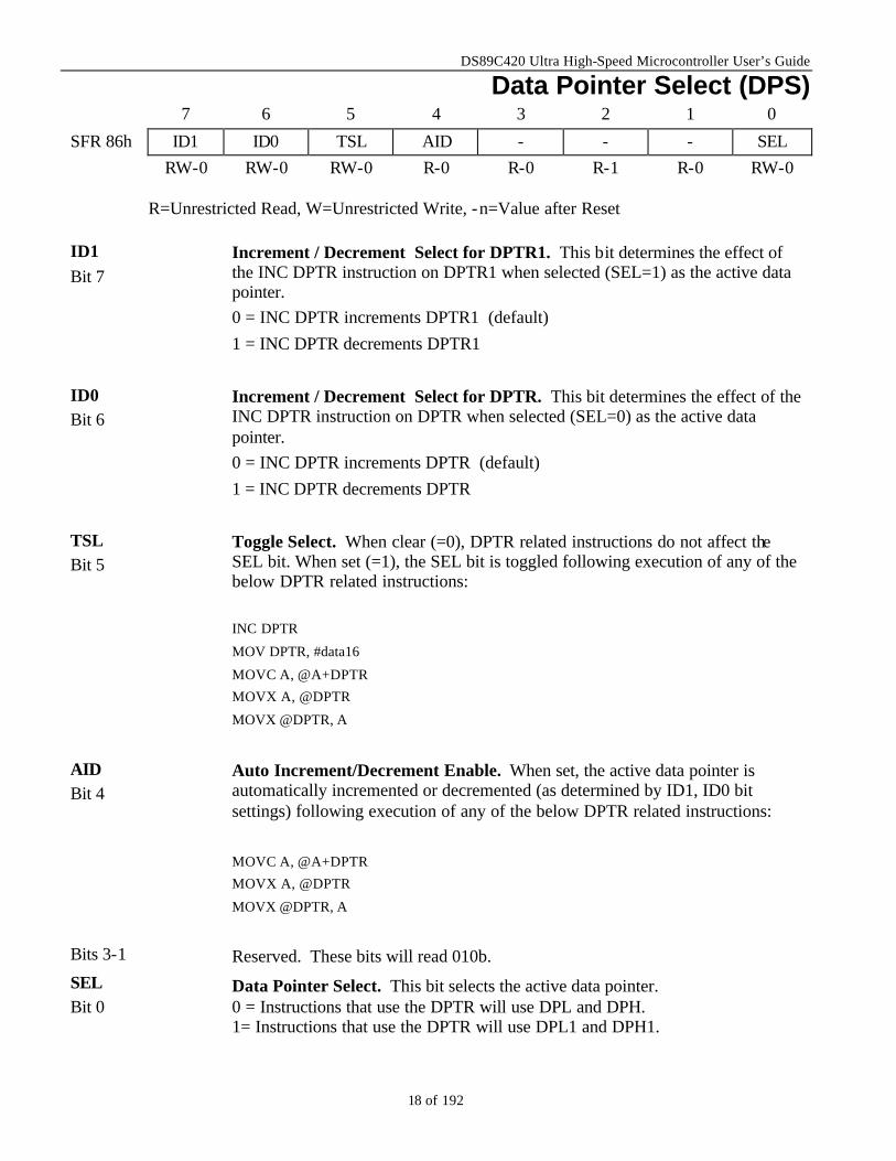
Data Pointer Select (DPS) 7 6 5 4 3 2 1 0
SFR 86h ID1 ID0 TSL AID - - - SEL RW-0 RW-0 RW-0 R-0 R-0 R-1 R-0 RW-0
R=Unrestricted Read, W=Unrestricted Write, -n=Value after Reset
ID1 Bit 7
Increment / Decrement Select for DPTR1. This bit determines the effect of the INC DPTR instruction on DPTR1 when selected (SEL=1) as the active data pointer. 0 = INC DPTR increments DPTR1 (default) 1 = INC DPTR decrements DPTR1
ID0 Bit 6
Increment / Decrement Select for DPTR. This bit determines the effect of the INC DPTR instruction on DPTR when selected (SEL=0) as the active data pointer. 0 = INC DPTR increments DPTR (default) 1 = INC DPTR decrements DPTR
TSL Bit 5
Toggle Select. When clear (=0), DPTR related instructions do not affect the SEL bit. When set (=1), the SEL bit is toggled following execution of any of the below DPTR related instructions:
INC DPTR
MOV DPTR, #data16
MOVC A, @A+DPTR
MOVX A, @DPTR
MOVX @DPTR, A
AID Bit 4
Auto Increment/Decrement Enable. When set, the active data pointer is automatically incremented or decremented (as determined by ID1, ID0 bit settings) following execution of any of the below DPTR related instructions: MOVC A, @A+DPTR
MOVX A, @DPTR
MOVX @DPTR, A
Bits 3-1 Reserved. These bits will read 010b. SEL Bit 0
Data Pointer Select. This bit selects the active data pointer. 0 = Instructions that use the DPTR will use DPL and DPH. 1= Instructions that use the DPTR will use DPL1 and DPH1.
DS89C420 Ultra High-Speed Microcontroller User’s Guide
19 of 192
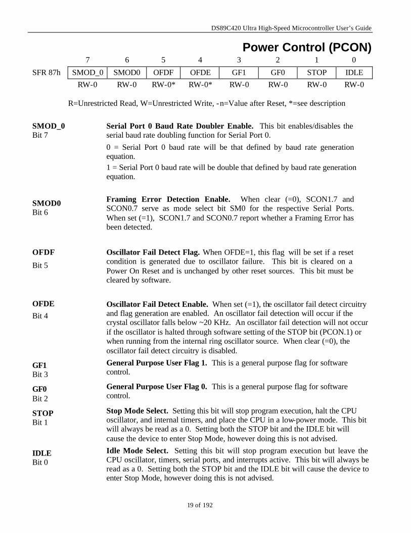
Power Control (PCON) 7 6 5 4 3 2 1 0
SFR 87h SMOD_0 SMOD0 OFDF OFDE GF1 GF0 STOP IDLE RW-0 RW-0 RW-0* RW-0* RW-0 RW-0 RW-0 RW-0
R=Unrestricted Read, W=Unrestricted Write, -n=Value after Reset, *=see description
SMOD_0 Bit 7
Serial Port 0 Baud Rate Doubler Enable. This bit enables/disables the serial baud rate doubling function for Serial Port 0. 0 = Serial Port 0 baud rate will be that defined by baud rate generation equation. 1 = Serial Port 0 baud rate will be double that defined by baud rate generation equation.
SMOD0 Bit 6
Framing Error Detection Enable. When clear (=0), SCON1.7 and SCON0.7 serve as mode select bit SM0 for the respective Serial Ports. When set (=1), SCON1.7 and SCON0.7 report whether a Framing Error has been detected.
OFDF
Bit 5
Oscillator Fail Detect Flag. When OFDE=1, this flag will be set if a reset condition is generated due to oscillator failure. This bit is cleared on a Power On Reset and is unchanged by other reset sources. This bit must be cleared by software.
OFDE Bit 4
Oscillator Fail Detect Enable. When set (=1), the oscillator fail detect circuitry and flag generation are enabled. An oscillator fail detection will occur if the crystal oscillator falls below ~20 KHz. An oscillator fail detection will not occur if the oscillator is halted through software setting of the STOP bit (PCON.1) or when running from the internal ring oscillator source. When clear (=0), the oscillator fail detect circuitry is disabled.
GF1 Bit 3
General Purpose User Flag 1. This is a general purpose flag for software control.
GF0 Bit 2
General Purpose User Flag 0. This is a general purpose flag for software control.
STOP Bit 1
Stop Mode Select. Setting this bit will stop program execution, halt the CPU oscillator, and internal timers, and place the CPU in a low-power mode. This bit will always be read as a 0. Setting both the STOP bit and the IDLE bit will cause the device to enter Stop Mode, however doing this is not advised.
IDLE Bit 0
Idle Mode Select. Setting this bit will stop program execution but leave the CPU oscillator, timers, serial ports, and interrupts active. This bit will always be read as a 0. Setting both the STOP bit and the IDLE bit will cause the device to enter Stop Mode, however doing this is not advised.
DS89C420 Ultra High-Speed Microcontroller User’s Guide
20 of 192
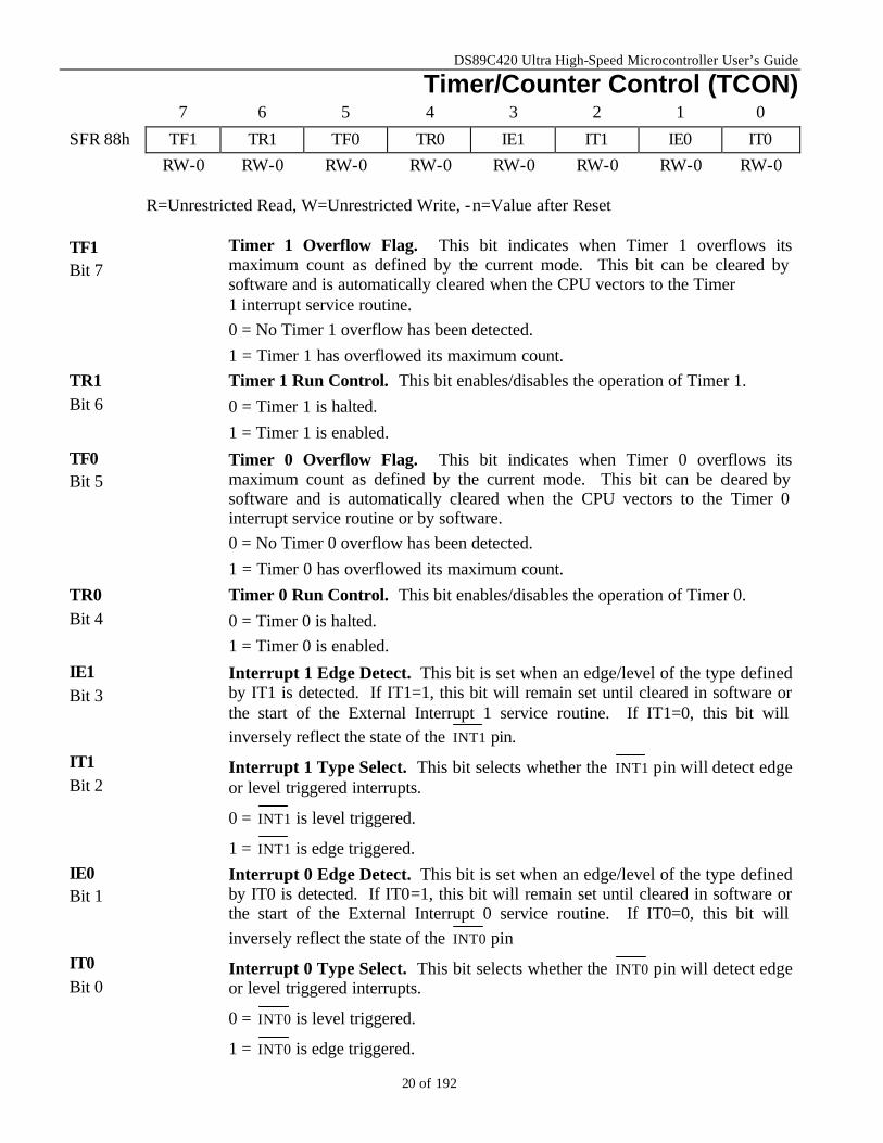
Timer/Counter Control (TCON) 7 6 5 4 3 2 1 0
SFR 88h TF1 TR1 TF0 TR0 IE1 IT1 IE0 IT0 RW-0 RW-0 RW-0 RW-0 RW-0 RW-0 RW-0 RW-0
R=Unrestricted Read, W=Unrestricted Write, -n=Value after Reset
TF1 Bit 7
Timer 1 Overflow Flag. This bit indicates when Timer 1 overflows its maximum count as defined by the current mode. This bit can be cleared by software and is automatically cleared when the CPU vectors to the Timer 1 interrupt service routine. 0 = No Timer 1 overflow has been detected. 1 = Timer 1 has overflowed its maximum count.
TR1 Bit 6
Timer 1 Run Control. This bit enables/disables the operation of Timer 1. 0 = Timer 1 is halted. 1 = Timer 1 is enabled.
TF0 Bit 5
Timer 0 Overflow Flag. This bit indicates when Timer 0 overflows its maximum count as defined by the current mode. This bit can be cleared by software and is automatically cleared when the CPU vectors to the Timer 0 interrupt service routine or by software. 0 = No Timer 0 overflow has been detected. 1 = Timer 0 has overflowed its maximum count.
TR0 Bit 4
Timer 0 Run Control. This bit enables/disables the operation of Timer 0. 0 = Timer 0 is halted. 1 = Timer 0 is enabled.
IE1 Bit 3
Interrupt 1 Edge Detect. This bit is set when an edge/level of the type defined by IT1 is detected. If IT1=1, this bit will remain set until cleared in software or the start of the External Interrupt 1 service routine. If IT1=0, this bit will inversely reflect the state of the INT1 pin.
IT1 Bit 2
Interrupt 1 Type Select. This bit selects whether the INT1 pin will detect edge or level triggered interrupts.
0 = INT1 is level triggered.
1 = INT1 is edge triggered. IE0 Bit 1
Interrupt 0 Edge Detect. This bit is set when an edge/level of the type defined by IT0 is detected. If IT0=1, this bit will remain set until cleared in software or the start of the External Interrupt 0 service routine. If IT0=0, this bit will inversely reflect the state of the INT0 pin
IT0 Bit 0
Interrupt 0 Type Select. This bit selects whether the INT0 pin will detect edge or level triggered interrupts.
0 = INT0 is level triggered.
1 = INT0 is edge triggered.
DS89C420 Ultra High-Speed Microcontroller User’s Guide
21 of 192
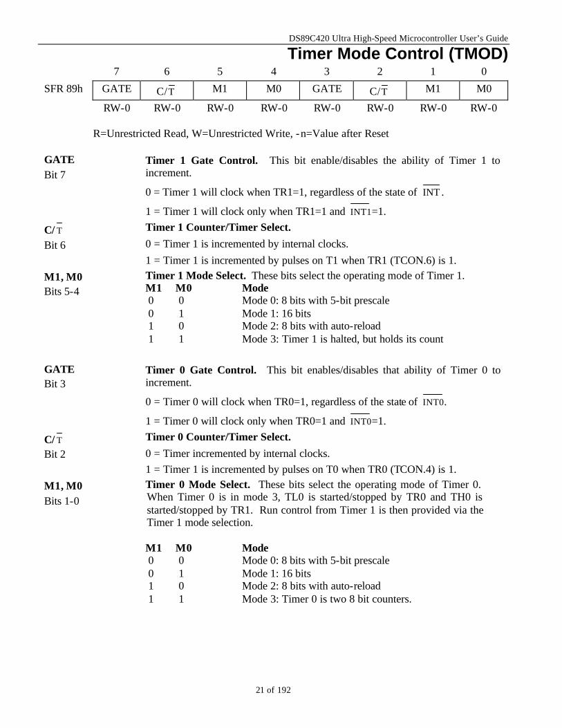
Timer Mode Control (TMOD) 7 6 5 4 3 2 1 0
SFR 89h GATE C/T M1 M0 GATE C/T M1 M0
RW-0 RW-0 RW-0 RW-0 RW-0 RW-0 RW-0 RW-0
R=Unrestricted Read, W=Unrestricted Write, -n=Value after Reset
GATE Bit 7
Timer 1 Gate Control. This bit enable/disables the ability of Timer 1 to increment.
0 = Timer 1 will clock when TR1=1, regardless of the state of INT .
1 = Timer 1 will clock only when TR1=1 and INT1=1.
C/ T Bit 6
Timer 1 Counter/Timer Select. 0 = Timer 1 is incremented by internal clocks. 1 = Timer 1 is incremented by pulses on T1 when TR1 (TCON.6) is 1.
M1, M0 Bits 5-4
Timer 1 Mode Select. These bits select the operating mode of Timer 1. M1 M0 Mode 0 0 Mode 0: 8 bits with 5-bit prescale 0 1 Mode 1: 16 bits 1 0 Mode 2: 8 bits with auto-reload 1 1 Mode 3: Timer 1 is halted, but holds its count
GATE Bit 3
Timer 0 Gate Control. This bit enables/disables that ability of Timer 0 to increment.
0 = Timer 0 will clock when TR0=1, regardless of the state of INT0.
1 = Timer 0 will clock only when TR0=1 and INT0=1.
C/ T Bit 2
Timer 0 Counter/Timer Select. 0 = Timer incremented by internal clocks. 1 = Timer 1 is incremented by pulses on T0 when TR0 (TCON.4) is 1.
M1, M0 Bits 1-0
Timer 0 Mode Select. These bits select the operating mode of Timer 0. When Timer 0 is in mode 3, TL0 is started/stopped by TR0 and TH0 is started/stopped by TR1. Run control from Timer 1 is then provided via the Timer 1 mode selection. M1 M0 Mode 0 0 Mode 0: 8 bits with 5-bit prescale 0 1 Mode 1: 16 bits 1 0 Mode 2: 8 bits with auto-reload 1 1 Mode 3: Timer 0 is two 8 bit counters.
DS89C420 Ultra High-Speed Microcontroller User’s Guide
22 of 192
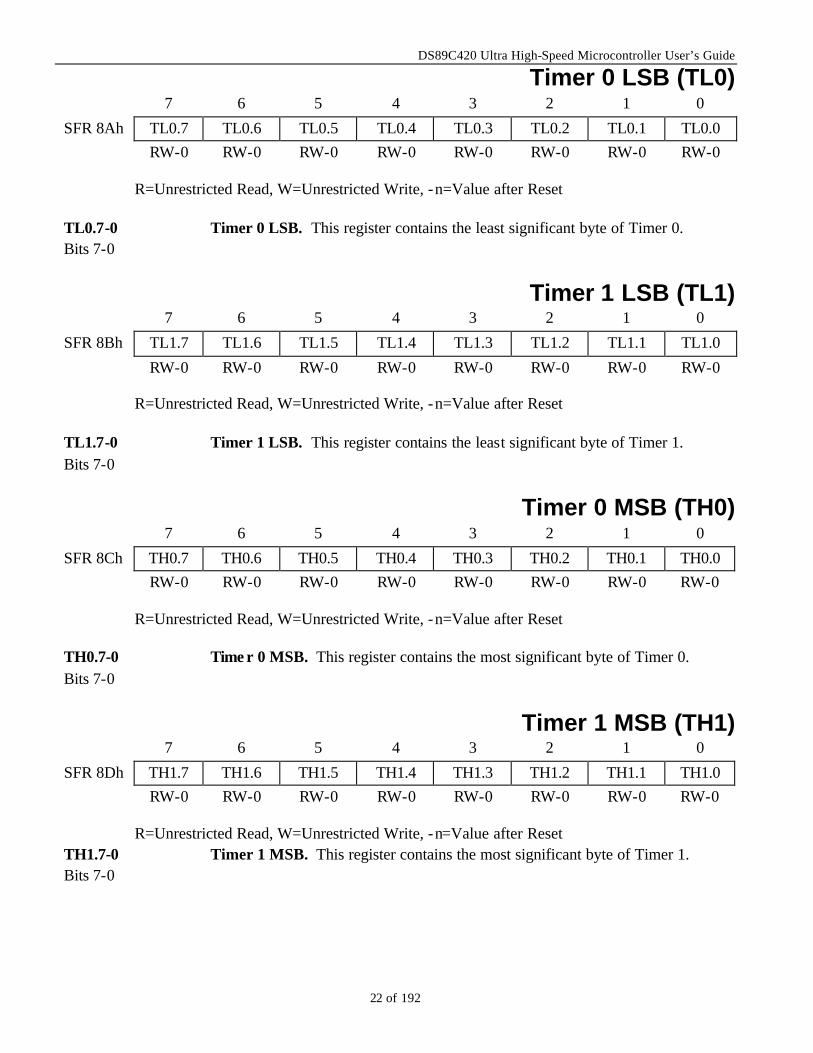
Timer 0 LSB (TL0) 7 6 5 4 3 2 1 0
SFR 8Ah TL0.7 TL0.6 TL0.5 TL0.4 TL0.3 TL0.2 TL0.1 TL0.0 RW-0 RW-0 RW-0 RW-0 RW-0 RW-0 RW-0 RW-0
R=Unrestricted Read, W=Unrestricted Write, -n=Value after Reset
TL0.7-0 Bits 7-0
Timer 0 LSB. This register contains the least significant byte of Timer 0.
Timer 1 LSB (TL1) 7 6 5 4 3 2 1 0
SFR 8Bh TL1.7 TL1.6 TL1.5 TL1.4 TL1.3 TL1.2 TL1.1 TL1.0 RW-0 RW-0 RW-0 RW-0 RW-0 RW-0 RW-0 RW-0
R=Unrestricted Read, W=Unrestricted Write, -n=Value after Reset
TL1.7-0 Bits 7-0
Timer 1 LSB. This register contains the least significant byte of Timer 1.
Timer 0 MSB (TH0) 7 6 5 4 3 2 1 0
SFR 8Ch TH0.7 TH0.6 TH0.5 TH0.4 TH0.3 TH0.2 TH0.1 TH0.0 RW-0 RW-0 RW-0 RW-0 RW-0 RW-0 RW-0 RW-0
R=Unrestricted Read, W=Unrestricted Write, -n=Value after Reset
TH0.7-0 Bits 7-0
Time r 0 MSB. This register contains the most significant byte of Timer 0.
Timer 1 MSB (TH1) 7 6 5 4 3 2 1 0
SFR 8Dh TH1.7 TH1.6 TH1.5 TH1.4 TH1.3 TH1.2 TH1.1 TH1.0 RW-0 RW-0 RW-0 RW-0 RW-0 RW-0 RW-0 RW-0
R=Unrestricted Read, W=Unrestricted Write, -n=Value after Reset
TH1.7-0 Bits 7-0
Timer 1 MSB. This register contains the most significant byte of Timer 1.
DS89C420 Ultra High-Speed Microcontroller User’s Guide
23 of 192
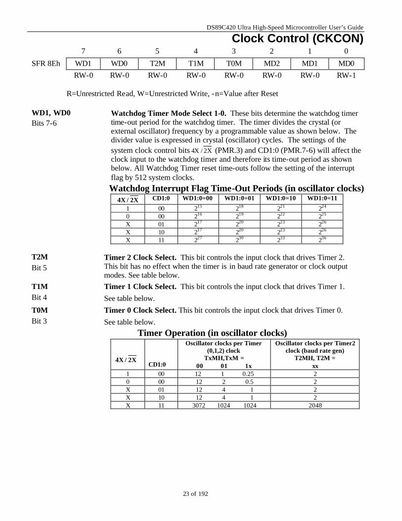
Clock Control (CKCON) 7 6 5 4 3 2 1 0
SFR 8Eh WD1 WD0 T2M T1M T0M MD2 MD1 MD0 RW-0 RW-0 RW-0 RW-0 RW-0 RW-0 RW-0 RW-1
R=Unrestricted Read, W=Unrestricted Write, -n=Value after Reset
WD1, WD0 Bits 7-6
Watchdog Timer Mode Select 1-0. These bits determine the watchdog timer time-out period for the watchdog timer. The timer divides the crystal (or external oscillator) frequency by a programmable value as shown below. The divider value is expressed in crystal (oscillator) cycles. The settings of the system clock control bits X2/X4 (PMR.3) and CD1:0 (PMR.7-6) will affect the clock input to the watchdog timer and therefore its time-out period as shown below. All Watchdog Timer reset time-outs follow the setting of the interrupt flag by 512 system clocks.
Watchdog Interrupt Flag Time-Out Periods (in oscillator clocks) X2/X4 CD1:0 WD1:0=00 WD1:0=01 WD1:0=10 WD1:0=11
1 00 215 218 221 224
0 00 216 219 222 225
X 01 217 220 223 226
X 10 217 220 223 226 X 11 227 230 233 236
T2M Bit 5
Timer 2 Clock Select. This bit controls the input clock that drives Timer 2. This bit has no effect when the timer is in baud rate generator or clock output modes. See table below.
T1M Bit 4
Timer 1 Clock Select. This bit controls the input clock that drives Timer 1. See table below.
T0M Bit 3
Timer 0 Clock Select. This bit controls the input clock that drives Timer 0. See table below.
Timer Operation (in oscillator clocks)
X2/X4
CD1:0
Oscillator clocks per Timer (0,1,2) clock
TxMH,TxM = 00 01 1x
Oscillator clocks per Timer2 clock (baud rate gen)
T2MH, T2M = xx
1 00 12 1 0.25 2
0 00 12 2 0.5 2
X 01 12 4 1 2
X 10 12 4 1 2 X 11 3072 1024 1024 2048
DS89C420 Ultra High-Speed Microcontroller User’s Guide
24 of 192
MD2, MD1, MD0 Bits 2-0
Stretch MOVX Select 2-0. These bits select the time by which external MOVX cycles are to be stretched. This allows slower memory or peripherals to be accessed without using ports or manual software intervention. The RD or WR strobe will be stretched by the specified interval, which will be transparent to the software except for the increased time to execute to MOVX instruction. All internal MOVX instructions are executed at the 2 machine cycle rate (0 stretch) independent of these bit settings.
DS89C420 Ultra High-Speed Microcontroller User’s Guide
25 of 192
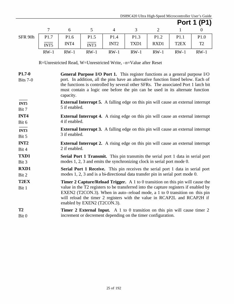
Port 1 (P1) 7 6 5 4 3 2 1 0
SFR 90h P1.7
INT5
P1.6 INT4
P1.5
INT3
P1.4 INT2
P1.3 TXD1
P1.2 RXD1
P1.1 T2EX
P1.0 T2
RW-1 RW-1 RW-1 RW-1 RW-1 RW-1 RW-1 RW-1
R=Unrestricted Read, W=Unrestricted Write, -n=Value after Reset
P1.7-0 Bits 7-0
General Purpose I/O Port 1. This register functions as a general purpose I/O port. In addition, all the pins have an alternative function listed below. Each of the functions is controlled by several other SFRs. The associated Port 1 latch bit must contain a logic one before the pin can be used in its alternate function capacity.
INT5 Bit 7
External Interrupt 5. A falling edge on this pin will cause an external interrupt 5 if enabled.
INT4 Bit 6
External Interrupt 4. A rising edge on this pin will cause an external interrupt 4 if enabled.
INT3 Bit 5
External Interrupt 3. A falling edge on this pin will cause an external interrupt 3 if enabled.
INT2 Bit 4
External Interrupt 2. A rising edge on this pin will cause an external interrupt 2 if enabled.
TXD1 Bit 3
Serial Port 1 Transmit. This pin transmits the serial port 1 data in serial port modes 1, 2, 3 and emits the synchronizing clock in serial port mode 0.
RXD1 Bit 2
Serial Port 1 Receive. This pin receives the serial port 1 data in serial port modes 1, 2, 3 and is a bi-directional data transfer pin in serial port mode 0.
T2EX Bit 1
Timer 2 Capture/Reload Trigger. A 1 to 0 transition on this pin will cause the value in the T2 registers to be transferred into the capture registers if enabled by EXEN2 (T2CON.3). When in auto–reload mode, a 1 to 0 transition on this pin will reload the timer 2 registers with the value in RCAP2L and RCAP2H if enabled by EXEN2 (T2CON.3).
T2 Bit 0
Timer 2 External Input. A 1 to 0 transition on this pin will cause timer 2 increment or decrement depending on the timer configuration.
DS89C420 Ultra High-Speed Microcontroller User’s Guide
26 of 192
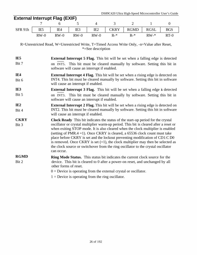
External Interrupt Flag (EXIF) 7 6 5 4 3 2 1 0
SFR 91h IE5 IE4 IE3 IE2 CKRY RGMD RGSL BGS RW-0 RW-0 RW-0 RW-0 R-* R-* RW-* RT-0
R=Unrestricted Read, W=Unrestricted Write, T=Timed Access Write Only, -n=Value after Reset,
*=See description
IE5 Bit 7
External Interrupt 5 Flag. This bit will be set when a falling edge is detected on INT5. This bit must be cleared manually by software. Setting this bit in software will cause an interrupt if enabled.
IE4 Bit 6
External Interrupt 4 Flag. This bit will be set when a rising edge is detected on INT4. This bit must be cleared manually by software. Setting this bit in software will cause an interrupt if enabled.
IE3 Bit 5
External Interrupt 3 Flag. This bit will be set when a falling edge is detected on INT3. This bit must be cleared manually by software. Setting this bit in software will cause an interrupt if enabled.
IE2 Bit 4
External Interrupt 2 Flag. This bit will be set when a rising edge is detected on INT2. This bit must be cleared manually by software. Setting this bit in software will cause an interrupt if enabled.
CKRY Bit 3
Clock Ready This bit indicates the status of the start-up period for the crystal oscillator or crystal multiplier warm-up period. This bit is cleared after a reset or when exiting STOP mode. It is also cleared when the clock multiplier is enabled (setting of PMR.4 =1). Once CKRY is cleared, a 65536 clock count must take place before CKRY is set and the lockout preventing modification of CD1:C D0 is removed. Once CKRY is set (=1), the clock multiplier may then be selected as the clock source or switchover from the ring oscillator to the crystal oscillator can occur.
RGMD Bit 2
Ring Mode Status. This status bit indicates the current clock source for the device. This bit is cleared to 0 after a power-on reset, and unchanged by all other forms of reset. 0 = Device is operating from the external crystal or oscillator. 1 = Device is operating from the ring oscillator.
DS89C420 Ultra High-Speed Microcontroller User’s Guide
27 of 192
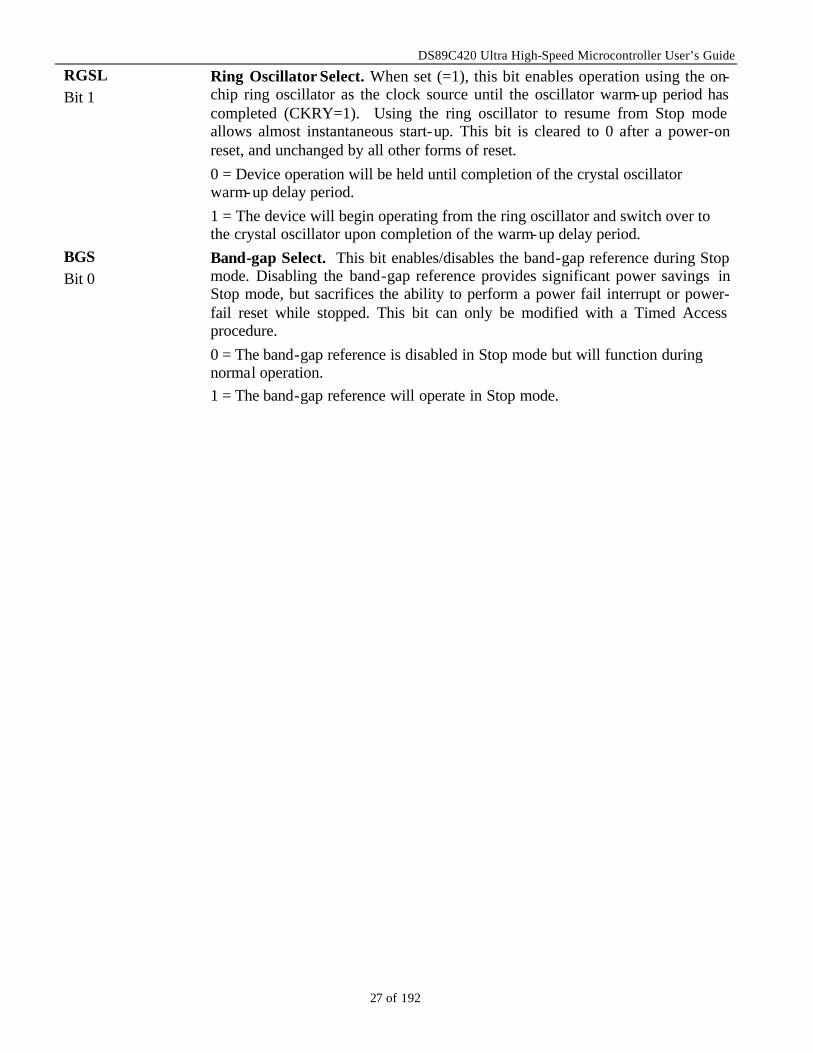
RGSL Bit 1
Ring Oscillator Select. When set (=1), this bit enables operation using the on- chip ring oscillator as the clock source until the oscillator warm-up period has completed (CKRY=1). Using the ring oscillator to resume from Stop mode allows almost instantaneous start-up. This bit is cleared to 0 after a power-on reset, and unchanged by all other forms of reset. 0 = Device operation will be held until completion of the crystal oscillator warm-up delay period. 1 = The device will begin operating from the ring oscillator and switch over to the crystal oscillator upon completion of the warm-up delay period.
BGS Bit 0
Band-gap Select. This bit enables/disables the band-gap reference during Stop mode. Disabling the band-gap reference provides significant power savings in Stop mode, but sacrifices the ability to perform a power fail interrupt or power-fail reset while stopped. This bit can only be modified with a Timed Access procedure. 0 = The band-gap reference is disabled in Stop mode but will function during normal operation. 1 = The band-gap reference will operate in Stop mode.

DS89C420 Ultra High-Speed Microcontroller User’s Guide
28 of 192
Timer and Serial Port Clock Mode Register (CKMOD) 7 6 5 4 3 2 1 0
SFR 96h - - T2MH T1MH T0MH - - - RW-1 RW-1 RW-0 RW-0 RW-0 RW-1 RW-1 RW-1
R=Unrestricted Read, W=Unrestricted Write, -n=Value after Reset
T2MH Bit 5
Timer 2 Clock Mode High Speed Select. When set (=1), the system clock will be used as the input clock for Timer 2 and the T2M bit (CKCON.5) setting will be ignored. When clear (=0), the input clock for Timer 2 will be selected using the T2M bit.
T1MH Bit 4
Timer 1 Clock Mode High Speed Select. When set (=1), the system clock will be used as the input clock for Timer 2 and the T1M bit (CKCON.4) setting will be ignored. When clear (=0), the input clock for Timer 2 will be selected using the T1M bit.
T0MH Bit 3
Timer 0 Clock Mode High Speed Select. When set (=1), the system clock will be used as the input clock for Timer 2 and the T0M bit (CKCON.3) setting will be ignored. When clear (=0), the input clock for Timer 2 will be selected using the T0M bit.
DS89C420 Ultra High-Speed Microcontroller User’s Guide
29 of 192
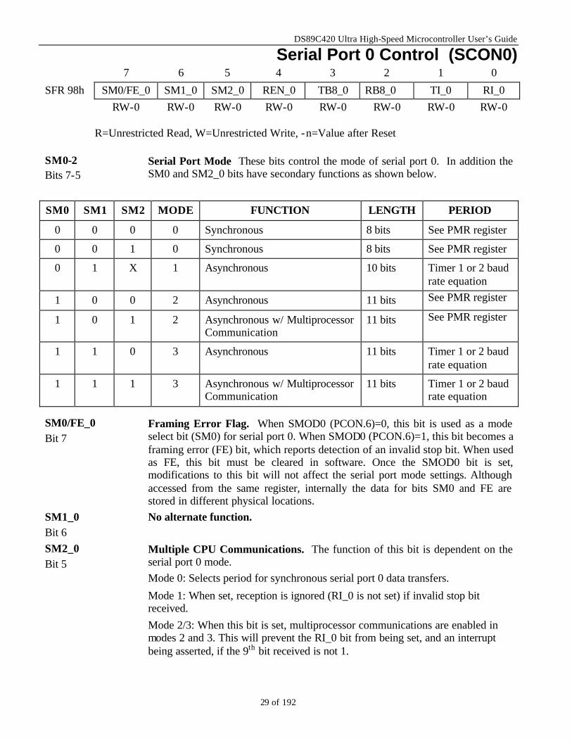
Serial Port 0 Control (SCON0) 7 6 5 4 3 2 1 0
SFR 98h SM0/FE_0 SM1_0 SM2_0 REN_0 TB8_0 RB8_0 TI_0 RI_0 RW-0 RW-0 RW-0 RW-0 RW-0 RW-0 RW-0 RW-0
R=Unrestricted Read, W=Unrestricted Write, -n=Value after Reset
SM0-2 Bits 7-5
Serial Port Mode These bits control the mode of serial port 0. In addition the SM0 and SM2_0 bits have secondary functions as shown below.
SM0 SM1 SM2 MODE FUNCTION LENGTH PERIOD
0 0 0 0 Synchronous 8 bits See PMR register
0 0 1 0 Synchronous 8 bits See PMR register
0 1 X 1 Asynchronous 10 bits Timer 1 or 2 baud rate equation
1 0 0 2 Asynchronous 11 bits See PMR register
1 0 1 2 Asynchronous w/ Multiprocessor Communication
11 bits See PMR register
1 1 0 3 Asynchronous 11 bits Timer 1 or 2 baud rate equation
1 1 1 3 Asynchronous w/ Multiprocessor Communication
11 bits Timer 1 or 2 baud rate equation
SM0/FE_0 Bit 7
Framing Error Flag. When SMOD0 (PCON.6)=0, this bit is used as a mode select bit (SM0) for serial port 0. When SMOD0 (PCON.6)=1, this bit becomes a framing error (FE) bit, which reports detection of an invalid stop bit. When used as FE, this bit must be cleared in software. Once the SMOD0 bit is set, modifications to this bit will not affect the serial port mode settings. Although accessed from the same register, internally the data for bits SM0 and FE are stored in different physical locations.
SM1_0 Bit 6
No alternate function.
SM2_0 Bit 5
Multiple CPU Communications. The function of this bit is dependent on the serial port 0 mode. Mode 0: Selects period for synchronous serial port 0 data transfers.
Mode 1: When set, reception is ignored (RI_0 is not set) if invalid stop bit received. Mode 2/3: When this bit is set, multiprocessor communications are enabled in modes 2 and 3. This will prevent the RI_0 bit from being set, and an interrupt being asserted, if the 9th bit received is not 1.
DS89C420 Ultra High-Speed Microcontroller User’s Guide
30 of 192
REN_0 Bit 4
Receiver Enable. This bit enable/disables the serial port 0 receiver shift register. 0 = Serial port 0 reception disabled. 1= Serial port 0 receiver enabled (modes 1, 2, 3). Initiate synchronous reception (mode 0).
TB8_0 Bit 3
9th Transmission Bit State. This bit defines the state of the 9th transmission bit in serial port 0 modes 2 and 3.
RB8_0 Bit 2
9th Received Bit State. This bit identifies that state of the 9th reception bit of received data in serial port 0 modes 2 and 3. In serial port mode 1, when SM2_0=0, RB8_0 is the state of the stop bit. RB8_0 is not used in mode 0.
TI_0 Bit 1
Transmitter Interrupt Flag. This bit indicates that data in the serial port 0 buffer has been completely shifted out. In serial port mode 0, TI_0 is set at the end of the 8th data bit. In all other modes, this bit is set at the end of the last data bit. This bit must be manually cleared by software.
RI_0 Bit 0
Receiver Interrupt Flag. This bit indicates that a byte of data has been received in the serial port 0 buffer. In serial port mode 0, RI_0 is set at the end of the 8th bit. In serial port mode 1, RI_0 is set after the last sample of the incoming stop bit subject to the state of SM2_0. In modes 2 and 3, RI_0 is set after the last sample of RB8_0. This bit must be manually cleared by software.
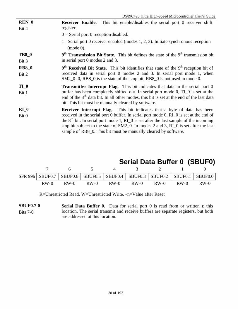
Serial Data Buffer 0 (SBUF0) 7 6 5 4 3 2 1 0
SFR 99h SBUF0.7 SBUF0.6 SBUF0.5 SBUF0.4 SBUF0.3 SBUF0.2 SBUF0.1 SBUF0.0 RW-0 RW-0 RW-0 RW-0 RW-0 RW-0 RW-0 RW-0
R=Unrestricted Read, W=Unrestricted Write, -n=Value after Reset
SBUF0.7-0 Bits 7-0
Serial Data Buffer 0. Data for serial port 0 is read from or written to this location. The serial transmit and receive buffers are separate registers, but both are addressed at this location.
DS89C420 Ultra High-Speed Microcontroller User’s Guide
31 of 192
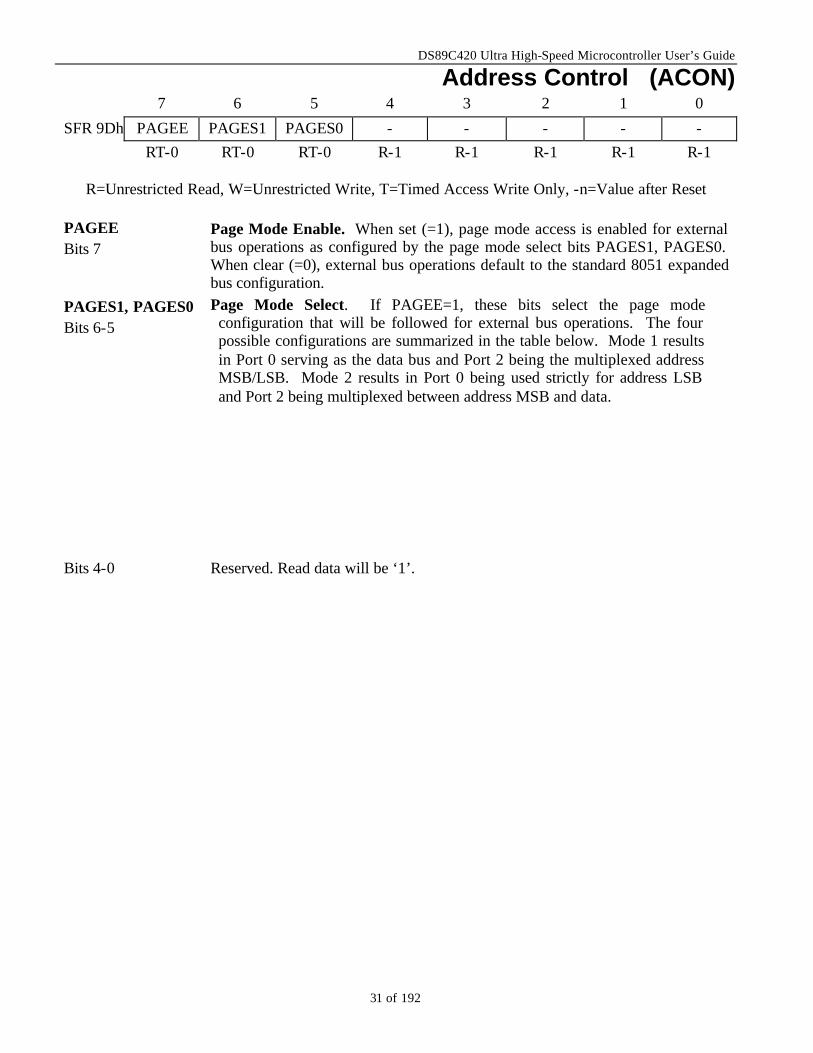
Address Control (ACON) 7 6 5 4 3 2 1 0
SFR 9Dh PAGEE PAGES1 PAGES0 - - - - - RT-0 RT-0 RT-0 R-1 R-1 R-1 R-1 R-1
R=Unrestricted Read, W=Unrestricted Write, T=Timed Access Write Only, -n=Value after Reset
PAGEE Bits 7
Page Mode Enable. When set (=1), page mode access is enabled for external bus operations as configured by the page mode select bits PAGES1, PAGES0. When clear (=0), external bus operations default to the standard 8051 expanded bus configuration.
PAGES1, PAGES0 Bits 6-5
Page Mode Select. If PAGEE=1, these bits select the page mode configuration that will be followed for external bus operations. The four possible configurations are summarized in the table below. Mode 1 results in Port 0 serving as the data bus and Port 2 being the multiplexed address MSB/LSB. Mode 2 results in Port 0 being used strictly for address LSB and Port 2 being multiplexed between address MSB and data.
Bits 4-0 Reserved. Read data will be ‘1’.
DS89C420 Ultra High-Speed Microcontroller User’s Guide
32 of 192
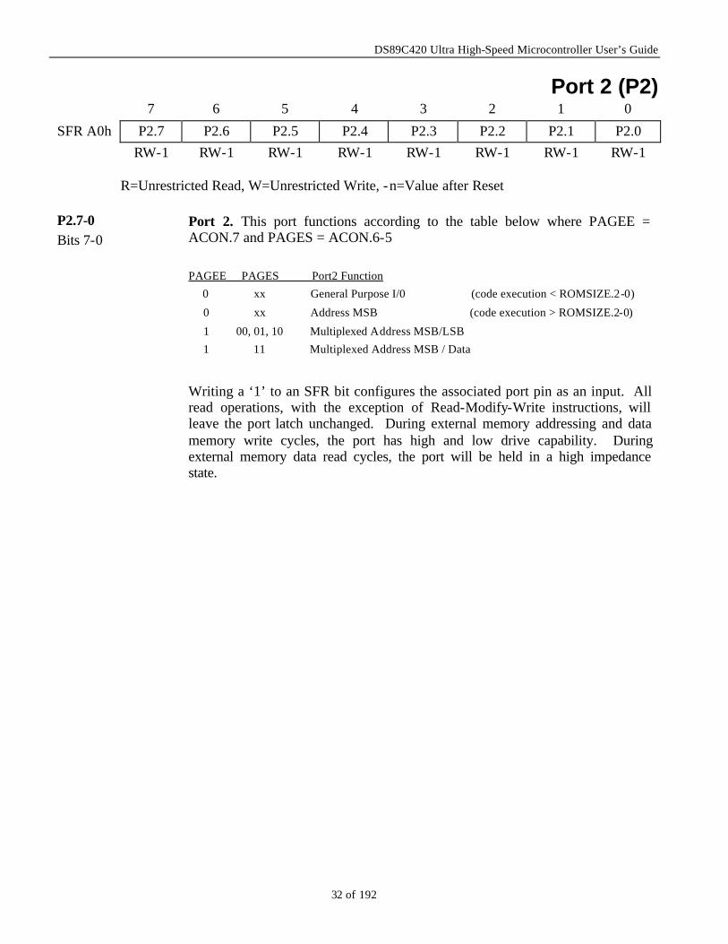
Port 2 (P2) 7 6 5 4 3 2 1 0
SFR A0h P2.7 P2.6 P2.5 P2.4 P2.3 P2.2 P2.1 P2.0 RW-1 RW-1 RW-1 RW-1 RW-1 RW-1 RW-1 RW-1
R=Unrestricted Read, W=Unrestricted Write, -n=Value after Reset
P2.7-0 Bits 7-0
Port 2. This port functions according to the table below where PAGEE = ACON.7 and PAGES = ACON.6-5
PAGEE PAGES Port2 Function
0 xx General Purpose I/0 (code execution < ROMSIZE.2-0)
0 xx Address MSB (code execution > ROMSIZE.2-0)
1 00, 01, 10 Multiplexed Address MSB/LSB
1 11 Multiplexed Address MSB / Data
Writing a ‘1’ to an SFR bit configures the associated port pin as an input. All read operations, with the exception of Read-Modify-Write instructions, will leave the port latch unchanged. During external memory addressing and data memory write cycles, the port has high and low drive capability. During external memory data read cycles, the port will be held in a high impedance state.
DS89C420 Ultra High-Speed Microcontroller User’s Guide
33 of 192
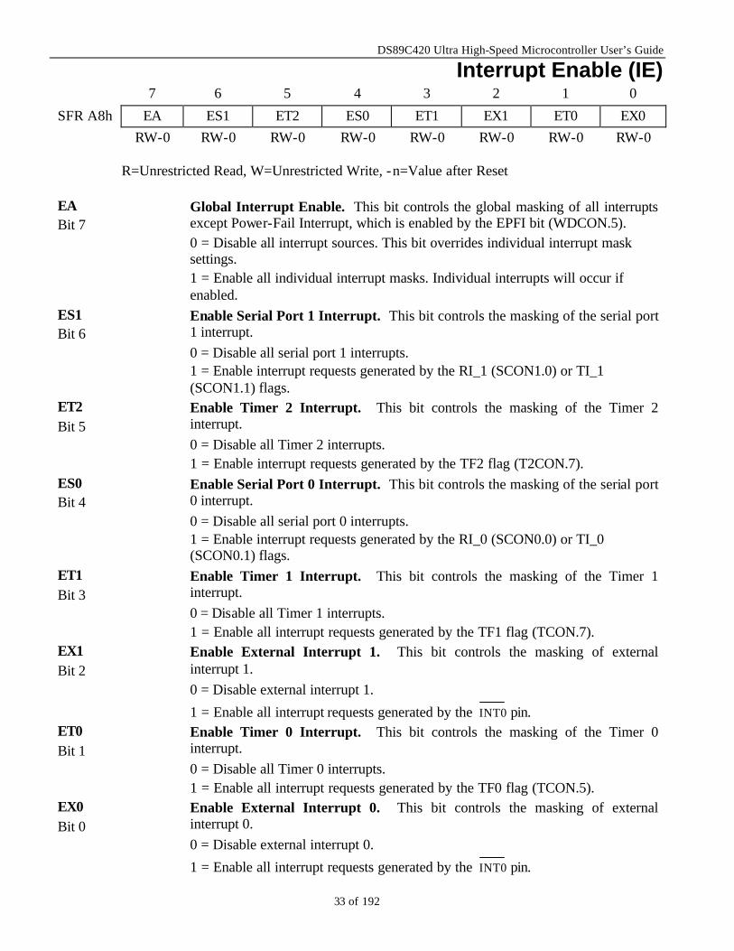
Interrupt Enable (IE) 7 6 5 4 3 2 1 0
SFR A8h EA ES1 ET2 ES0 ET1 EX1 ET0 EX0 RW-0 RW-0 RW-0 RW-0 RW-0 RW-0 RW-0 RW-0
R=Unrestricted Read, W=Unrestricted Write, -n=Value after Reset
EA Bit 7
Global Interrupt Enable. This bit controls the global masking of all interrupts except Power-Fail Interrupt, which is enabled by the EPFI bit (WDCON.5). 0 = Disable all interrupt sources. This bit overrides individual interrupt mask settings. 1 = Enable all individual interrupt masks. Individual interrupts will occur if enabled.
ES1 Bit 6
Enable Serial Port 1 Interrupt. This bit controls the masking of the serial port 1 interrupt. 0 = Disable all serial port 1 interrupts. 1 = Enable interrupt requests generated by the RI_1 (SCON1.0) or TI_1 (SCON1.1) flags.
ET2 Bit 5
Enable Timer 2 Interrupt. This bit controls the masking of the Timer 2 interrupt. 0 = Disable all Timer 2 interrupts. 1 = Enable interrupt requests generated by the TF2 flag (T2CON.7).
ES0 Bit 4
Enable Serial Port 0 Interrupt. This bit controls the masking of the serial port 0 interrupt. 0 = Disable all serial port 0 interrupts. 1 = Enable interrupt requests generated by the RI_0 (SCON0.0) or TI_0 (SCON0.1) flags.
ET1 Bit 3
Enable Timer 1 Interrupt. This bit controls the masking of the Timer 1 interrupt. 0 = Disable all Timer 1 interrupts. 1 = Enable all interrupt requests generated by the TF1 flag (TCON.7).
EX1 Bit 2
Enable External Interrupt 1. This bit controls the masking of external interrupt 1. 0 = Disable external interrupt 1.
1 = Enable all interrupt requests generated by the INT0 pin. ET0 Bit 1
Enable Timer 0 Interrupt. This bit controls the masking of the Timer 0 interrupt. 0 = Disable all Timer 0 interrupts. 1 = Enable all interrupt requests generated by the TF0 flag (TCON.5).
EX0 Bit 0
Enable External Interrupt 0. This bit controls the masking of external interrupt 0. 0 = Disable external interrupt 0.
1 = Enable all interrupt requests generated by the INT0 pin.
DS89C420 Ultra High-Speed Microcontroller User’s Guide
34 of 192
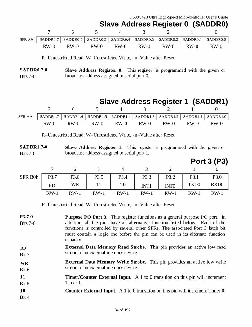
Slave Address Register 0 (SADDR0) 7 6 5 4 3 2 1 0
SFR A9h SADDR0.7 SADDR0.6 SADDR0.5 SADDR0.4 SADDR0.3 SADDR0.2 SADDR0.1 SADDR0.0
RW-0 RW-0 RW-0 RW-0 RW-0 RW-0 RW-0 RW-0
R=Unrestricted Read, W=Unrestricted Write, -n=Value after Reset
SADDR0.7-0 Bits 7-0
Slave Address Register 0. This register is programmed with the given or broadcast address assigned to serial port 0.
Slave Address Register 1 (SADDR1) 7 6 5 4 3 2 1 0
SFR AAh SADDR1.7 SADDR1.6 SADDR1.5 SADDR1.4 SADDR1.3 SADDR1.2 SADDR1.1 SADDR1.0
RW-0 RW-0 RW-0 RW-0 RW-0 RW-0 RW-0 RW-0
R=Unrestricted Read, W=Unrestricted Write, -n=Value after Reset
SADDR1.7-0 Bits 7-0
Slave Address Register 1. This register is programmed with the given or broadcast address assigned to serial port 1.
Port 3 (P3) 7 6 5 4 3 2 1 0
SFR B0h P3.7
RD
P3.6 WR
P3.5 T1
P3.4 T0
P3.3
INT1
P3.2
INT0
P3.1 TXD0
P3.0 RXD0
RW-1 RW-1 RW-1 RW-1 RW-1 RW-1 RW-1 RW-1
R=Unrestricted Read, W=Unrestricted Write, -n=Value after Reset
P3.7-0 Bits 7-0
Purpose I/O Port 3. This register functions as a general purpose I/O port. In addition, all the pins have an alternative function listed below. Each of the functions is controlled by several other SFRs. The associated Port 3 latch bit must contain a logic one before the pin can be used in its alternate function capacity.
RD Bit 7
External Data Memory Read Strobe. This pin provides an active low read strobe to an external memory device.
WR Bit 6
External Data Memory Write Strobe. This pin provides an active low write strobe to an external memory device.
T1 Bit 5
Timer/Counter External Input. A 1 to 0 transition on this pin will increment Timer 1.
T0 Bit 4
Counter External Input. A 1 to 0 transition on this pin will increment Timer 0.
DS89C420 Ultra High-Speed Microcontroller User’s Guide
35 of 192
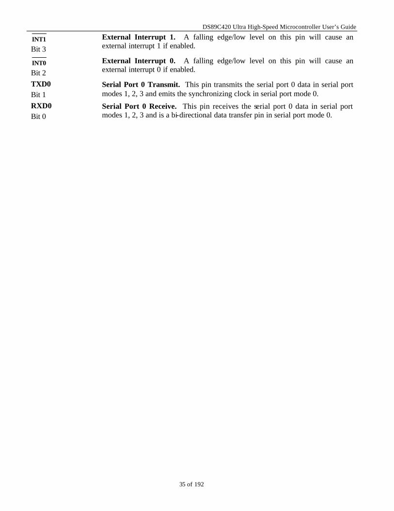
INT1 Bit 3
External Interrupt 1. A falling edge/low level on this pin will cause an external interrupt 1 if enabled.
INT0 Bit 2
External Interrupt 0. A falling edge/low level on this pin will cause an external interrupt 0 if enabled.
TXD0 Bit 1
Serial Port 0 Transmit. This pin transmits the serial port 0 data in serial port modes 1, 2, 3 and emits the synchronizing clock in serial port mode 0.
RXD0 Bit 0
Serial Port 0 Receive. This pin receives the serial port 0 data in serial port modes 1, 2, 3 and is a bi-directional data transfer pin in serial port mode 0.
DS89C420 Ultra High-Speed Microcontroller User’s Guide
36 of 192
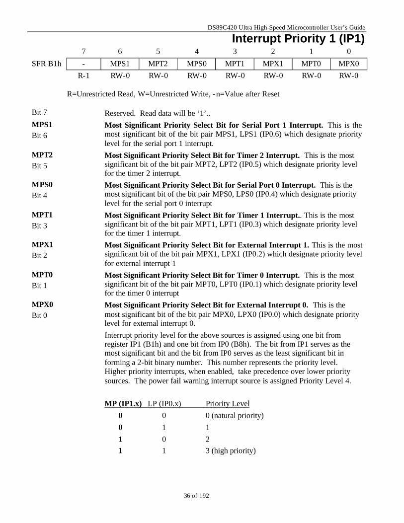
Interrupt Priority 1 (IP1) 7 6 5 4 3 2 1 0
SFR B1h - MPS1 MPT2 MPS0 MPT1 MPX1 MPT0 MPX0 R-1 RW-0 RW-0 RW-0 RW-0 RW-0 RW-0 RW-0
R=Unrestricted Read, W=Unrestricted Write, -n=Value after Reset
Bit 7 Reserved. Read data will be ‘1’.. MPS1 Bit 6
Most Significant Priority Select Bit for Serial Port 1 Interrupt. This is the most significant bit of the bit pair MPS1, LPS1 (IP0.6) which designate priority level for the serial port 1 interrupt.
MPT2 Bit 5
Most Significant Priority Select Bit for Timer 2 Interrupt. This is the most significant bit of the bit pair MPT2, LPT2 (IP0.5) which designate priority level for the timer 2 interrupt.
MPS0 Bit 4
Most Significant Priority Select Bit for Serial Port 0 Interrupt. This is the most significant bit of the bit pair MPS0, LPS0 (IP0.4) which designate priority level for the serial port 0 interrupt
MPT1 Bit 3
Most Significant Priority Select Bit for Timer 1 Interrupt.. This is the most significant bit of the bit pair MPT1, LPT1 (IP0.3) which designate priority level for the timer 1 interrupt.
MPX1 Bit 2
Most Significant Priority Select Bit for External Interrupt 1. This is the most significant bit of the bit pair MPX1, LPX1 (IP0.2) which designate priority level for external interrupt 1
MPT0 Bit 1
Most Significant Priority Select Bit for Timer 0 Interrupt. This is the most significant bit of the bit pair MPT0, LPT0 (IP0.1) which designate priority level for the timer 0 interrupt
MPX0 Bit 0
Most Significant Priority Select Bit for External Interrupt 0. This is the most significant bit of the bit pair MPX0, LPX0 (IP0.0) which designate priority level for external interrupt 0.
Interrupt priority level for the above sources is assigned using one bit from register IP1 (B1h) and one bit from IP0 (B8h). The bit from IP1 serves as the most significant bit and the bit from IP0 serves as the least significant bit in forming a 2-bit binary number. This number represents the priority level. Higher priority interrupts, when enabled, take precedence over lower priority sources. The power fail warning interrupt source is assigned Priority Level 4. MP (IP1.x) LP (IP0.x) Priority Level 0 0 0 (natural priority) 0 1 1 1 0 2 1 1 3 (high priority)
DS89C420 Ultra High-Speed Microcontroller User’s Guide
37 of 192
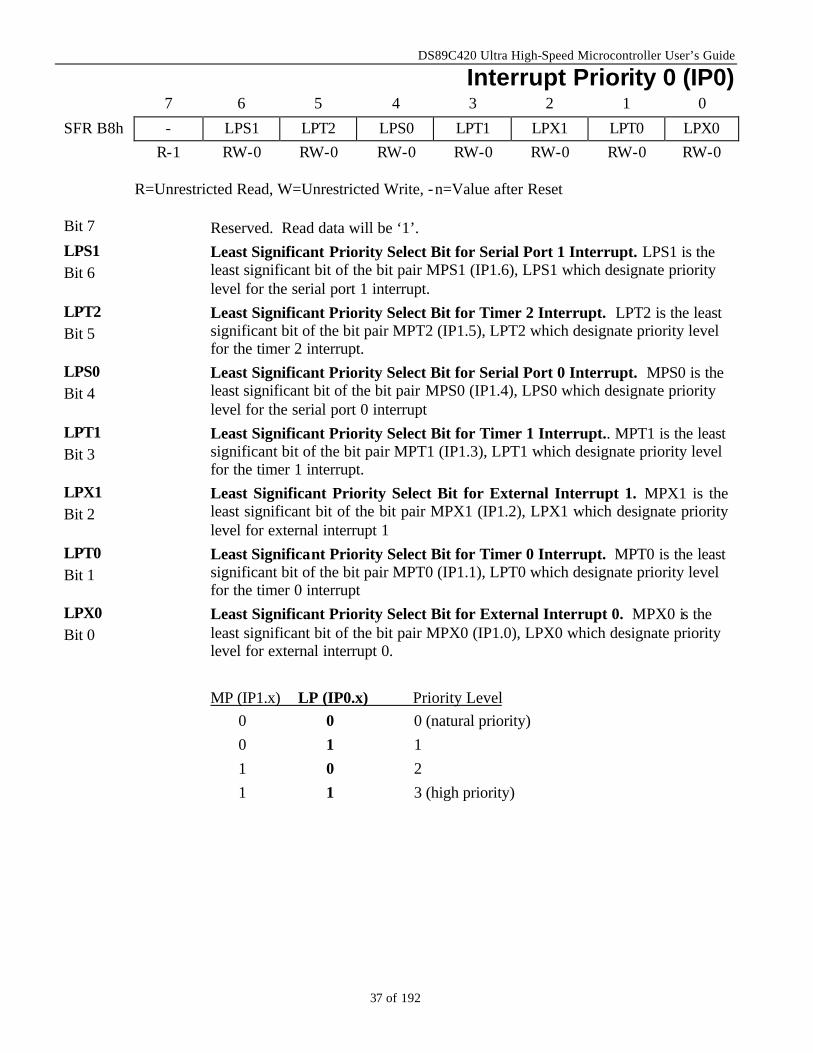
Interrupt Priority 0 (IP0) 7 6 5 4 3 2 1 0
SFR B8h - LPS1 LPT2 LPS0 LPT1 LPX1 LPT0 LPX0 R-1 RW-0 RW-0 RW-0 RW-0 RW-0 RW-0 RW-0
R=Unrestricted Read, W=Unrestricted Write, -n=Value after Reset
Bit 7 Reserved. Read data will be ‘1’. LPS1 Bit 6
Least Significant Priority Select Bit for Serial Port 1 Interrupt. LPS1 is the least significant bit of the bit pair MPS1 (IP1.6), LPS1 which designate priority level for the serial port 1 interrupt.
LPT2 Bit 5
Least Significant Priority Select Bit for Timer 2 Interrupt. LPT2 is the least significant bit of the bit pair MPT2 (IP1.5), LPT2 which designate priority level for the timer 2 interrupt.
LPS0 Bit 4
Least Significant Priority Select Bit for Serial Port 0 Interrupt. MPS0 is the least significant bit of the bit pair MPS0 (IP1.4), LPS0 which designate priority level for the serial port 0 interrupt
LPT1 Bit 3
Least Significant Priority Select Bit for Timer 1 Interrupt.. MPT1 is the least significant bit of the bit pair MPT1 (IP1.3), LPT1 which designate priority level for the timer 1 interrupt.
LPX1 Bit 2
Least Significant Priority Select Bit for External Interrupt 1. MPX1 is the least significant bit of the bit pair MPX1 (IP1.2), LPX1 which designate priority level for external interrupt 1
LPT0 Bit 1
Least Significant Priority Select Bit for Timer 0 Interrupt. MPT0 is the least significant bit of the bit pair MPT0 (IP1.1), LPT0 which designate priority level for the timer 0 interrupt
LPX0 Bit 0
Least Significant Priority Select Bit for External Interrupt 0. MPX0 is the least significant bit of the bit pair MPX0 (IP1.0), LPX0 which designate priority level for external interrupt 0.
MP (IP1.x) LP (IP0.x) Priority Level 0 0 0 (natural priority) 0 1 1 1 0 2 1 1 3 (high priority)
DS89C420 Ultra High-Speed Microcontroller User’s Guide
38 of 192
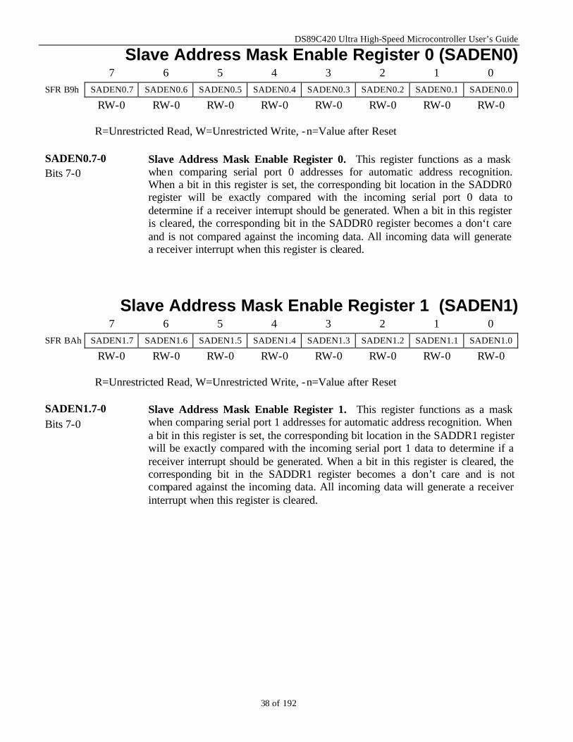
Slave Address Mask Enable Register 0 (SADEN0) 7 6 5 4 3 2 1 0
SFR B9h SADEN0.7 SADEN0.6 SADEN0.5 SADEN0.4 SADEN0.3 SADEN0.2 SADEN0.1 SADEN0.0
RW-0 RW-0 RW-0 RW-0 RW-0 RW-0 RW-0 RW-0
R=Unrestricted Read, W=Unrestricted Write, -n=Value after Reset
SADEN0.7-0 Bits 7-0
Slave Address Mask Enable Register 0. This register functions as a mask when comparing serial port 0 addresses for automatic address recognition. When a bit in this register is set, the corresponding bit location in the SADDR0 register will be exactly compared with the incoming serial port 0 data to determine if a receiver interrupt should be generated. When a bit in this register is cleared, the corresponding bit in the SADDR0 register becomes a don‘t care and is not compared against the incoming data. All incoming data will generate a receiver interrupt when this register is cleared.
Slave Address Mask Enable Register 1 (SADEN1) 7 6 5 4 3 2 1 0
SFR BAh SADEN1.7 SADEN1.6 SADEN1.5 SADEN1.4 SADEN1.3 SADEN1.2 SADEN1.1 SADEN1.0
RW-0 RW-0 RW-0 RW-0 RW-0 RW-0 RW-0 RW-0
R=Unrestricted Read, W=Unrestricted Write, -n=Value after Reset
SADEN1.7-0 Bits 7-0
Slave Address Mask Enable Register 1. This register functions as a mask when comparing serial port 1 addresses for automatic address recognition. When a bit in this register is set, the corresponding bit location in the SADDR1 register will be exactly compared with the incoming serial port 1 data to determine if a receiver interrupt should be generated. When a bit in this register is cleared, the corresponding bit in the SADDR1 register becomes a don’t care and is not compared against the incoming data. All incoming data will generate a receiver interrupt when this register is cleared.
DS89C420 Ultra High-Speed Microcontroller User’s Guide
39 of 192
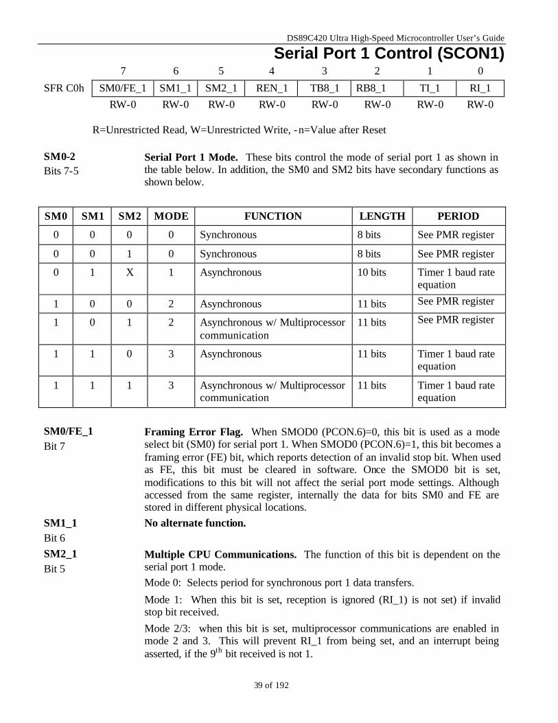
Serial Port 1 Control (SCON1) 7 6 5 4 3 2 1 0
SFR C0h SM0/FE_1 SM1_1 SM2_1 REN_1 TB8_1 RB8_1 TI_1 RI_1 RW-0 RW-0 RW-0 RW-0 RW-0 RW-0 RW-0 RW-0
R=Unrestricted Read, W=Unrestricted Write, -n=Value after Reset
SM0-2 Bits 7-5
Serial Port 1 Mode. These bits control the mode of serial port 1 as shown in the table below. In addition, the SM0 and SM2 bits have secondary functions as shown below.
SM0 SM1 SM2 MODE FUNCTION LENGTH PERIOD
0 0 0 0 Synchronous 8 bits See PMR register
0 0 1 0 Synchronous 8 bits See PMR register
0 1 X 1 Asynchronous 10 bits Timer 1 baud rate equation
1 0 0 2 Asynchronous 11 bits See PMR register
1 0 1 2 Asynchronous w/ Multiprocessor communication
11 bits See PMR register
1 1 0 3 Asynchronous 11 bits Timer 1 baud rate equation
1 1 1 3 Asynchronous w/ Multiprocessor communication
11 bits Timer 1 baud rate equation
SM0/FE_1 Bit 7
Framing Error Flag. When SMOD0 (PCON.6)=0, this bit is used as a mode select bit (SM0) for serial port 1. When SMOD0 (PCON.6)=1, this bit becomes a framing error (FE) bit, which reports detection of an invalid stop bit. When used as FE, this bit must be cleared in software. Once the SMOD0 bit is set, modifications to this bit will not affect the serial port mode settings. Although accessed from the same register, internally the data for bits SM0 and FE are stored in different physical locations.
SM1_1 Bit 6
No alternate function.
SM2_1 Bit 5
Multiple CPU Communications. The function of this bit is dependent on the serial port 1 mode. Mode 0: Selects period for synchronous port 1 data transfers.
Mode 1: When this bit is set, reception is ignored (RI_1) is not set) if invalid stop bit received. Mode 2/3: when this bit is set, multiprocessor communications are enabled in mode 2 and 3. This will prevent RI_1 from being set, and an interrupt being asserted, if the 9th bit received is not 1.
DS89C420 Ultra High-Speed Microcontroller User’s Guide
40 of 192
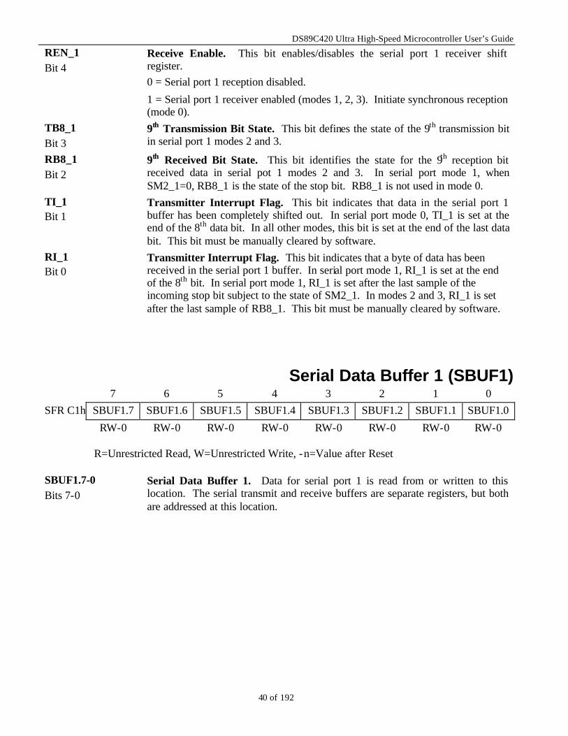
REN_1 Bit 4
Receive Enable. This bit enables/disables the serial port 1 receiver shift register. 0 = Serial port 1 reception disabled.
1 = Serial port 1 receiver enabled (modes 1, 2, 3). Initiate synchronous reception (mode 0).
TB8_1 Bit 3
9th Transmission Bit State. This bit defines the state of the 9th transmission bit in serial port 1 modes 2 and 3.
RB8_1 Bit 2
9th Received Bit State. This bit identifies the state for the 9th reception bit received data in serial pot 1 modes 2 and 3. In serial port mode 1, when SM2_1=0, RB8_1 is the state of the stop bit. RB8_1 is not used in mode 0.
TI_1 Bit 1
Transmitter Interrupt Flag. This bit indicates that data in the serial port 1 buffer has been completely shifted out. In serial port mode 0, TI_1 is set at the end of the 8th data bit. In all other modes, this bit is set at the end of the last data bit. This bit must be manually cleared by software.
RI_1 Bit 0
Transmitter Interrupt Flag. This bit indicates that a byte of data has been received in the serial port 1 buffer. In serial port mode 1, RI_1 is set at the end of the 8th bit. In serial port mode 1, RI_1 is set after the last sample of the incoming stop bit subject to the state of SM2_1. In modes 2 and 3, RI_1 is set after the last sample of RB8_1. This bit must be manually cleared by software.
Serial Data Buffer 1 (SBUF1) 7 6 5 4 3 2 1 0
SFR C1h SBUF1.7 SBUF1.6 SBUF1.5 SBUF1.4 SBUF1.3 SBUF1.2 SBUF1.1 SBUF1.0 RW-0 RW-0 RW-0 RW-0 RW-0 RW-0 RW-0 RW-0
R=Unrestricted Read, W=Unrestricted Write, -n=Value after Reset
SBUF1.7-0 Bits 7-0
Serial Data Buffer 1. Data for serial port 1 is read from or written to this location. The serial transmit and receive buffers are separate registers, but both are addressed at this location.
DS89C420 Ultra High-Speed Microcontroller User’s Guide
41 of 192
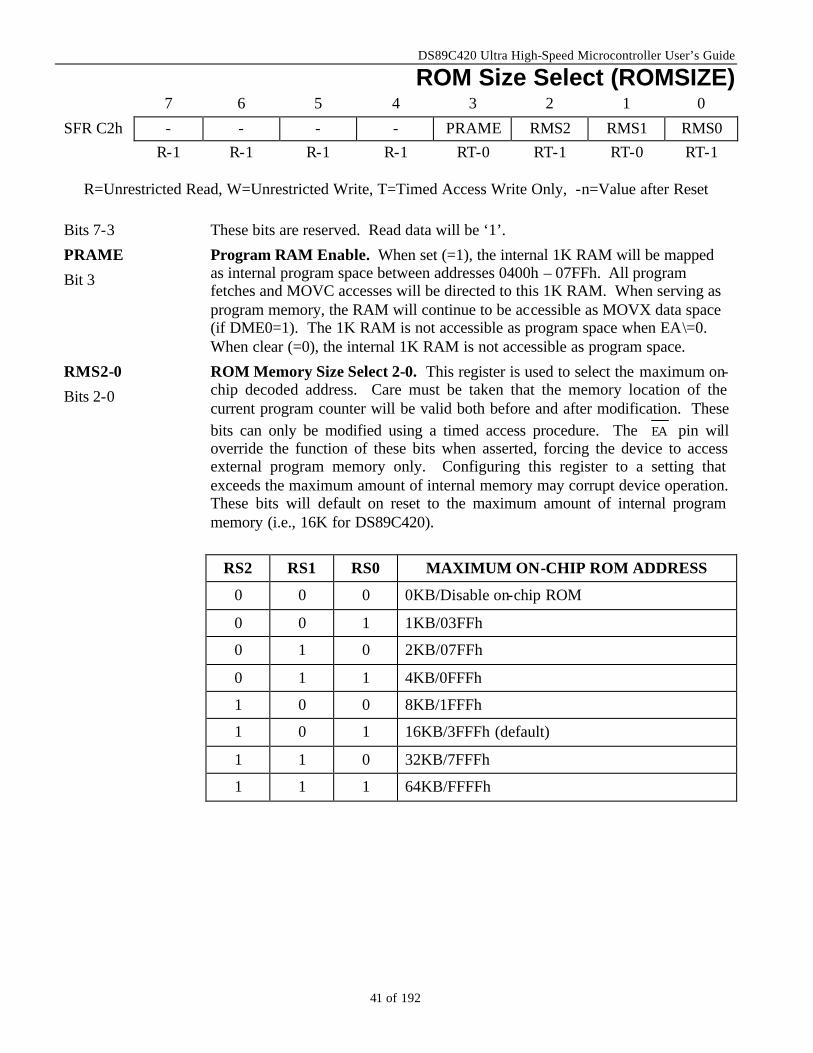
ROM Size Select (ROMSIZE) 7 6 5 4 3 2 1 0
SFR C2h - - - - PRAME RMS2 RMS1 RMS0 R-1 R-1 R-1 R-1 RT-0 RT-1 RT-0 RT-1
R=Unrestricted Read, W=Unrestricted Write, T=Timed Access Write Only, -n=Value after Reset
Bits 7-3 These bits are reserved. Read data will be ‘1’.
PRAME
Bit 3
Program RAM Enable. When set (=1), the internal 1K RAM will be mapped as internal program space between addresses 0400h – 07FFh. All program fetches and MOVC accesses will be directed to this 1K RAM. When serving as program memory, the RAM will continue to be accessible as MOVX data space (if DME0=1). The 1K RAM is not accessible as program space when EA\=0. When clear (=0), the internal 1K RAM is not accessible as program space.
RMS2-0
Bits 2-0
ROM Memory Size Select 2-0. This register is used to select the maximum on-chip decoded address. Care must be taken that the memory location of the current program counter will be valid both before and after modification. These bits can only be modified using a timed access procedure. The EA pin will override the function of these bits when asserted, forcing the device to access external program memory only. Configuring this register to a setting that exceeds the maximum amount of internal memory may corrupt device operation. These bits will default on reset to the maximum amount of internal program memory (i.e., 16K for DS89C420).
RS2 RS1 RS0 MAXIMUM ON-CHIP ROM ADDRESS
0 0 0 0KB/Disable on-chip ROM
0 0 1 1KB/03FFh
0 1 0 2KB/07FFh
0 1 1 4KB/0FFFh
1 0 0 8KB/1FFFh
1 0 1 16KB/3FFFh (default)
1 1 0 32KB/7FFFh
1 1 1 64KB/FFFFh
DS89C420 Ultra High-Speed Microcontroller User’s Guide
42 of 192
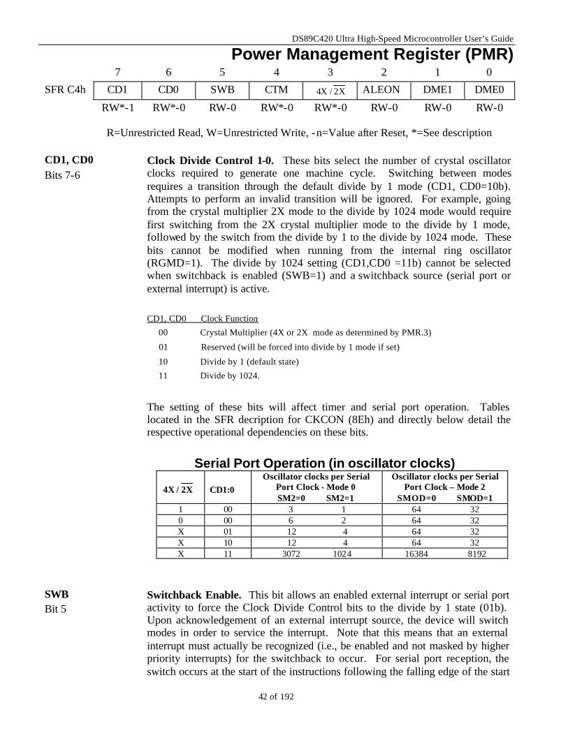
Power Management Register (PMR) 7 6 5 4 3 2 1 0
SFR C4h CD1 CD0 SWB CTM X2/X4 ALEON DME1 DME0 RW*-1 RW*-0 RW-0 RW*-0 RW*-0 RW-0 RW-0 RW-0
R=Unrestricted Read, W=Unrestricted Write, -n=Value after Reset, *=See description
CD1, CD0 Bits 7-6
Clock Divide Control 1-0. These bits select the number of crystal oscillator clocks required to generate one machine cycle. Switching between modes requires a transition through the default divide by 1 mode (CD1, CD0=10b). Attempts to perform an invalid transition will be ignored. For example, going from the crystal multiplier 2X mode to the divide by 1024 mode would require first switching from the 2X crystal multiplier mode to the divide by 1 mode, followed by the switch from the divide by 1 to the divide by 1024 mode. These bits cannot be modified when running from the internal ring oscillator (RGMD=1). The divide by 1024 setting (CD1,CD0 =11b) cannot be selected when switchback is enabled (SWB=1) and a switchback source (serial port or external interrupt) is active.
CD1, CD0 Clock Function
00 Crystal Multiplier (4X or 2X mode as determined by PMR.3)
01 Reserved (will be forced into divide by 1 mode if set)
10 Divide by 1 (default state)
11 Divide by 1024.
The setting of these bits will affect timer and serial port operation. Tables located in the SFR decription for CKCON (8Eh) and directly below detail the respective operational dependencies on these bits.
Serial Port Operation (in oscillator clocks)
X2/X4
CD1:0
Oscillator clocks per Serial Port Clock - Mode 0 SM2=0 SM2=1
Oscillator clocks per Serial Port Clock – Mode 2
SMOD=0 SMOD=1 1 00 3 1 64 32
0 00 6 2 64 32
X 01 12 4 64 32
X 10 12 4 64 32
X 11 3072 1024 16384 8192
SWB Bit 5
Switchback Enable. This bit allows an enabled external interrupt or serial port activity to force the Clock Divide Control bits to the divide by 1 state (01b). Upon acknowledgement of an external interrupt source, the device will switch modes in order to service the interrupt. Note that this means that an external interrupt must actually be recognized (i.e., be enabled and not masked by higher priority interrupts) for the switchback to occur. For serial port reception, the switch occurs at the start of the instructions following the falling edge of the start bit.
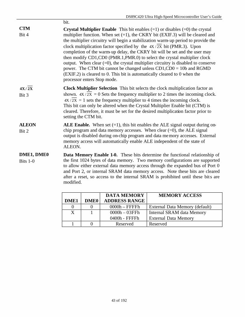
DS89C420 Ultra High-Speed Microcontroller User’s Guide
43 of 192
bit. CTM Bit 4
Crystal Multiplier Enable This bit enables (=1) or disables (=0) the crystal multiplier function. When set (=1), the CKRY bit (EXIF.3) will be cleared and the multiplier circuitry will begin a stabilization warm-up period to provide the clock multiplication factor specified by the X2/X4 bit (PMR.3). Upon completion of the warm-up delay, the CKRY bit will be set and the user may then modify CD1,CD0 (PMR.1,PMR.0) to select the crystal multiplier clock output. When clear (=0), the crystal multiplier circuitry is disabled to conserve power. The CTM bit cannot be changed unless CD1,CD0 = 10b and RGMD (EXIF.2) is cleared to 0. This bit is automatically cleared to 0 when the processor enters Stop mode.
X2/X4 Bit 3
Clock Multiplier Selection This bit selects the clock multiplication factor as shown. X2/X4 = 0 Sets the frequency multiplier to 2 times the incoming clock.
X2/X4 = 1 sets the frequency multiplier to 4 times the incoming clock. This bit can only be altered when the Crystal Multiplier Enable bit (CTM) is cleared. Therefore, it must be set for the desired multiplication factor prior to setting the CTM bit.
ALEON Bit 2
ALE Enable. When set (=1), this bit enables the ALE signal output during on-chip program and data memory accesses. When clear (=0), the ALE signal output is disabled during on-chip program and data memory accesses. External memory access will automatically enable ALE independent of the state of ALEON.
DME1, DME0 Bits 1-0
Data Memory Enable 1-0. These bits determine the functional relationship of the first 1024 bytes of data memory. Two memory configurations are supported to allow either external data memory access through the expanded bus of Port 0 and Port 2, or internal SRAM data memory access. Note these bits are cleared after a reset, so access to the internal SRAM is prohibited until these bit s are modified.
DME1
DME0 DATA MEMORY
ADDRESS RANGE MEMORY ACCESS
0 0 0000h – FFFFh External Data Memory (default) X 1 0000h – 03FFh
0400h - FFFFh Internal SRAM data Memory External Data Memory
1 0 Reserved Reserved
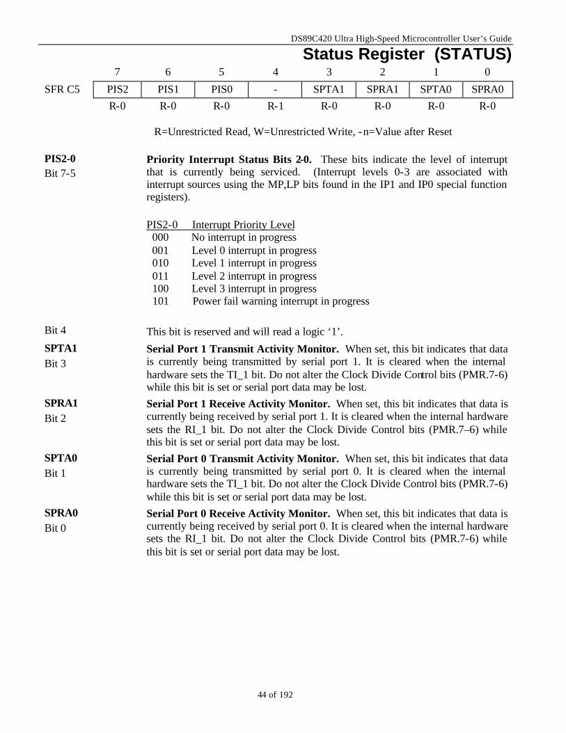
DS89C420 Ultra High-Speed Microcontroller User’s Guide
44 of 192
Status Register (STATUS) 7 6 5 4 3 2 1 0
SFR C5 PIS2 PIS1 PIS0 - SPTA1 SPRA1 SPTA0 SPRA0 R-0 R-0 R-0 R-1 R-0 R-0 R-0 R-0
R=Unrestricted Read, W=Unrestricted Write, -n=Value after Reset
PIS2-0 Bit 7-5
Priority Interrupt Status Bits 2-0. These bits indicate the level of interrupt that is currently being serviced. (Interrupt levels 0-3 are associated with interrupt sources using the MP,LP bits found in the IP1 and IP0 special function registers). PIS2-0 Interrupt Priority Level 000 No interrupt in progress 001 Level 0 interrupt in progress 010 Level 1 interrupt in progress 011 Level 2 interrupt in progress 100 Level 3 interrupt in progress 101 Power fail warning interrupt in progress
Bit 4 This bit is reserved and will read a logic ‘1’. SPTA1 Bit 3
Serial Port 1 Transmit Activity Monitor. When set, this bit indicates that data is currently being transmitted by serial port 1. It is cleared when the internal hardware sets the TI_1 bit. Do not alter the Clock Divide Control bits (PMR.7-6) while this bit is set or serial port data may be lost.
SPRA1 Bit 2
Serial Port 1 Receive Activity Monitor. When set, this bit indicates that data is currently being received by serial port 1. It is cleared when the internal hardware sets the RI_1 bit. Do not alter the Clock Divide Control bits (PMR.7–6) while this bit is set or serial port data may be lost.
SPTA0 Bit 1
Serial Port 0 Transmit Activity Monitor. When set, this bit indicates that data is currently being transmitted by serial port 0. It is cleared when the internal hardware sets the TI_1 bit. Do not alter the Clock Divide Control bits (PMR.7-6) while this bit is set or serial port data may be lost.
SPRA0 Bit 0
Serial Port 0 Receive Activity Monitor. When set, this bit indicates that data is currently being received by serial port 0. It is cleared when the internal hardware sets the RI_1 bit. Do not alter the Clock Divide Control bits (PMR.7-6) while this bit is set or serial port data may be lost.
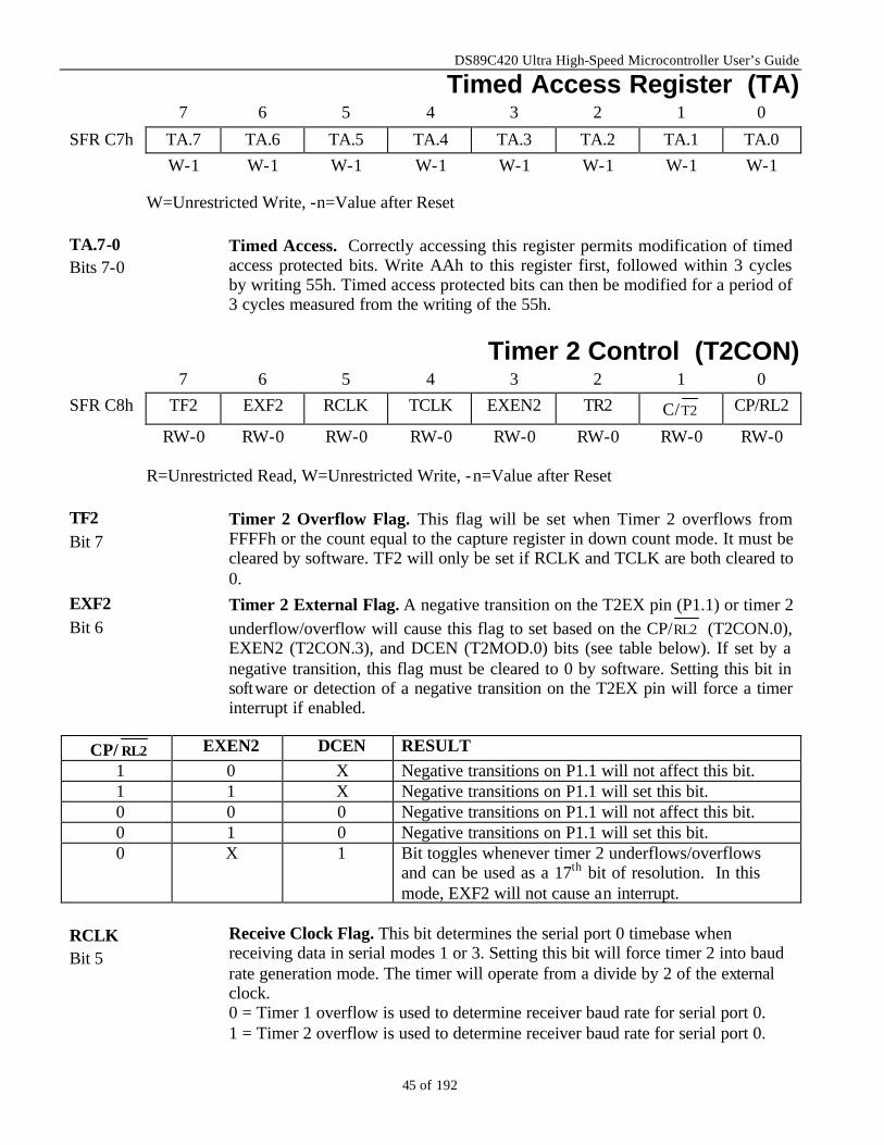
DS89C420 Ultra High-Speed Microcontroller User’s Guide
45 of 192
Timed Access Register (TA) 7 6 5 4 3 2 1 0
SFR C7h TA.7 TA.6 TA.5 TA.4 TA.3 TA.2 TA.1 TA.0 W-1 W-1 W-1 W-1 W-1 W-1 W-1 W-1
W=Unrestricted Write, -n=Value after Reset
TA.7-0 Bits 7-0
Timed Access. Correctly accessing this register permits modification of timed access protected bits. Write AAh to this register first, followed within 3 cycles by writing 55h. Timed access protected bits can then be modified for a period of 3 cycles measured from the writing of the 55h.
Timer 2 Control (T2CON) 7 6 5 4 3 2 1 0
SFR C8h TF2 EXF2 RCLK TCLK EXEN2 TR2 C/T2 CP/RL2
RW-0 RW-0 RW-0 RW-0 RW-0 RW-0 RW-0 RW-0
R=Unrestricted Read, W=Unrestricted Write, -n=Value after Reset
TF2 Bit 7
Timer 2 Overflow Flag. This flag will be set when Timer 2 overflows from FFFFh or the count equal to the capture register in down count mode. It must be cleared by software. TF2 will only be set if RCLK and TCLK are both cleared to 0.
EXF2 Bit 6
Timer 2 External Flag. A negative transition on the T2EX pin (P1.1) or timer 2 underflow/overflow will cause this flag to set based on the CP/RL2 (T2CON.0), EXEN2 (T2CON.3), and DCEN (T2MOD.0) bits (see table below). If set by a negative transition, this flag must be cleared to 0 by software. Setting this bit in software or detection of a negative transition on the T2EX pin will force a timer interrupt if enabled.
CP/ RL2 EXEN2 DCEN RESULT 1 0 X Negative transitions on P1.1 will not affect this bit. 1 1 X Negative transitions on P1.1 will set this bit. 0 0 0 Negative transitions on P1.1 will not affect this bit. 0 1 0 Negative transitions on P1.1 will set this bit. 0 X 1 Bit toggles whenever timer 2 underflows/overflows
and can be used as a 17th bit of resolution. In this mode, EXF2 will not cause an interrupt.
RCLK Bit 5
Receive Clock Flag. This bit determines the serial port 0 timebase when receiving data in serial modes 1 or 3. Setting this bit will force timer 2 into baud rate generation mode. The timer will operate from a divide by 2 of the external clock. 0 = Timer 1 overflow is used to determine receiver baud rate for serial port 0. 1 = Timer 2 overflow is used to determine receiver baud rate for serial port 0.
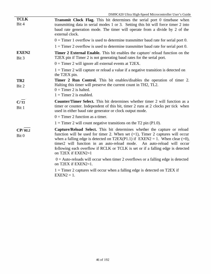
DS89C420 Ultra High-Speed Microcontroller User’s Guide
46 of 192
TCLK Bit 4
Transmit Clock Flag. This bit determines the serial port 0 timebase when transmitting data in serial modes 1 or 3. Setting this bit will force timer 2 into baud rate generation mode. The timer will operate from a divide by 2 of the external clock. 0 = Timer 1 overflow is used to determine transmitter baud rate for serial port 0. 1 = Timer 2 overflow is used to determine transmitter baud rate for serial port 0.
EXEN2 Bit 3
Timer 2 External Enable. This bit enables the capture/ reload function on the T2EX pin if Timer 2 is not generating baud rates for the serial port. 0 = Timer 2 will ignore all external events at T2EX.
1 = Timer 2 will capture or reload a value if a negative transition is detected on the T2EX pin.
TR2 Bit 2
Timer 2 Run Control. This bit enables/disables the operation of timer 2. Halting this timer will preserve the current count in TH2, TL2. 0 = Timer 2 is halted. 1 = Timer 2 is enabled.
C/ T2 Bit 1
Counter/Timer Select. This bit determines whether timer 2 will function as a timer or counter. Independent of this bit, timer 2 runs at 2 clocks per tick when used in either baud rate generator or clock output mode. 0 = Timer 2 function as a timer. 1 = Timer 2 will count negative transitions on the T2 pin (P1.0).
CP/ RL2 Bit 0
Capture/Reload Select. This bit determines whether the capture or reload function will be used for timer 2. When set (=1), Timer 2 captures will occur when a falling edge is detected on T2EX(P1.1) if EXEN2 = 1. When clear (=0), timer2 will function in an auto-reload mode. An auto-reload will occur following each overflow if RCLK or TCLK is set or if a falling edge is detected on T2EX if EXEN2=1 0 = Auto-reloads will occur when timer 2 overflows or a falling edge is detected on T2EX if EXEN2=1. 1 = Timer 2 captures will occur when a falling edge is detected on T2EX if EXEN2 = 1.
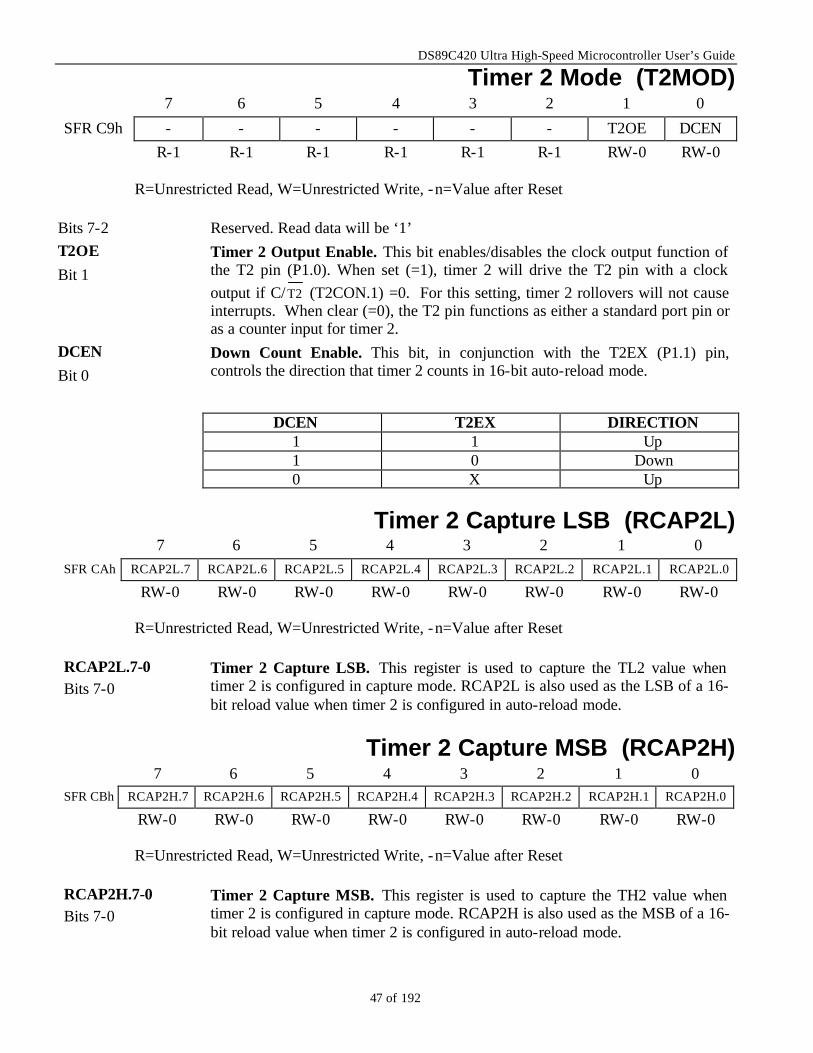
DS89C420 Ultra High-Speed Microcontroller User’s Guide
47 of 192
Timer 2 Mode (T2MOD) 7 6 5 4 3 2 1 0
SFR C9h - - - - - - T2OE DCEN R-1 R-1 R-1 R-1 R-1 R-1 RW-0 RW-0
R=Unrestricted Read, W=Unrestricted Write, -n=Value after Reset
Bits 7-2 Reserved. Read data will be ‘1’ T2OE Bit 1
Timer 2 Output Enable. This bit enables/disables the clock output function of the T2 pin (P1.0). When set (=1), timer 2 will drive the T2 pin with a clock output if C/ T2 (T2CON.1) =0. For this setting, timer 2 rollovers will not cause interrupts. When clear (=0), the T2 pin functions as either a standard port pin or as a counter input for timer 2.
DCEN Bit 0
Down Count Enable. This bit, in conjunction with the T2EX (P1.1) pin, controls the direction that timer 2 counts in 16-bit auto-reload mode.
DCEN T2EX DIRECTION
1 1 Up 1 0 Down 0 X Up
Timer 2 Capture LSB (RCAP2L) 7 6 5 4 3 2 1 0
SFR CAh RCAP2L.7 RCAP2L.6 RCAP2L.5 RCAP2L.4 RCAP2L.3 RCAP2L.2 RCAP2L.1 RCAP2L.0
RW-0 RW-0 RW-0 RW-0 RW-0 RW-0 RW-0 RW-0
R=Unrestricted Read, W=Unrestricted Write, -n=Value after Reset
RCAP2L.7-0 Bits 7-0
Timer 2 Capture LSB. This register is used to capture the TL2 value when timer 2 is configured in capture mode. RCAP2L is also used as the LSB of a 16-bit reload value when timer 2 is configured in auto-reload mode.
Timer 2 Capture MSB (RCAP2H) 7 6 5 4 3 2 1 0
SFR CBh RCAP2H.7 RCAP2H.6 RCAP2H.5 RCAP2H.4 RCAP2H.3 RCAP2H.2 RCAP2H.1 RCAP2H.0
RW-0 RW-0 RW-0 RW-0 RW-0 RW-0 RW-0 RW-0
R=Unrestricted Read, W=Unrestricted Write, -n=Value after Reset
RCAP2H.7-0 Bits 7-0
Timer 2 Capture MSB. This register is used to capture the TH2 value when timer 2 is configured in capture mode. RCAP2H is also used as the MSB of a 16-bit reload value when timer 2 is configured in auto-reload mode.
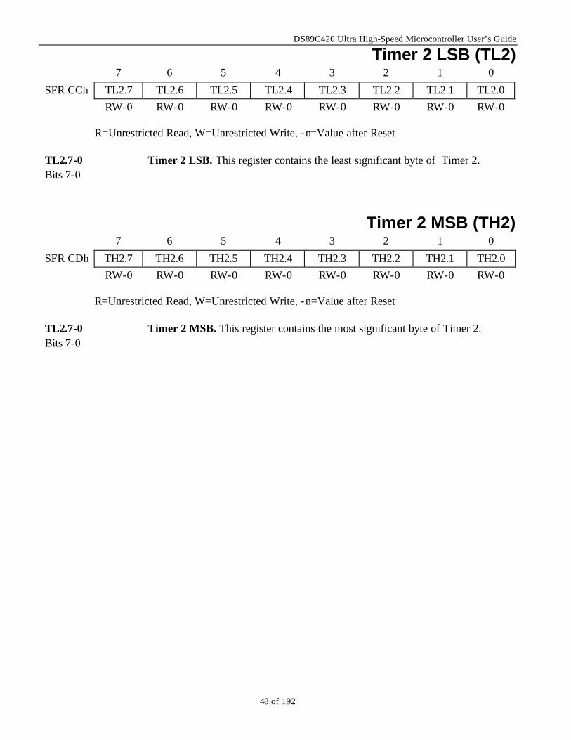
DS89C420 Ultra High-Speed Microcontroller User’s Guide
48 of 192
Timer 2 LSB (TL2) 7 6 5 4 3 2 1 0
SFR CCh TL2.7 TL2.6 TL2.5 TL2.4 TL2.3 TL2.2 TL2.1 TL2.0 RW-0 RW-0 RW-0 RW-0 RW-0 RW-0 RW-0 RW-0
R=Unrestricted Read, W=Unrestricted Write, -n=Value after Reset
TL2.7-0 Bits 7-0
Timer 2 LSB. This register contains the least significant byte of Timer 2.
Timer 2 MSB (TH2) 7 6 5 4 3 2 1 0
SFR CDh TH2.7 TH2.6 TH2.5 TH2.4 TH2.3 TH2.2 TH2.1 TH2.0 RW-0 RW-0 RW-0 RW-0 RW-0 RW-0 RW-0 RW-0
R=Unrestricted Read, W=Unrestricted Write, -n=Value after Reset
TL2.7-0 Bits 7-0
Timer 2 MSB. This register contains the most significant byte of Timer 2.
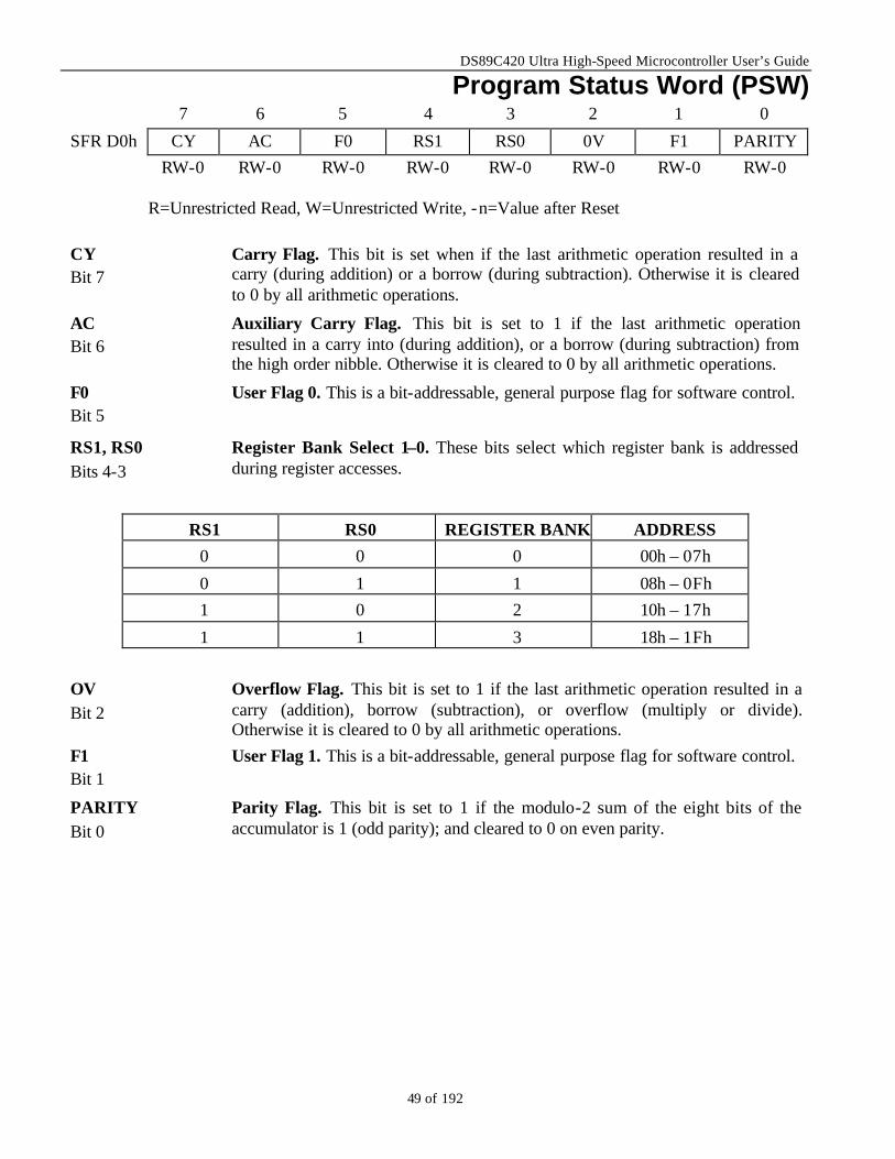
DS89C420 Ultra High-Speed Microcontroller User’s Guide
49 of 192
Program Status Word (PSW) 7 6 5 4 3 2 1 0
SFR D0h CY AC F0 RS1 RS0 0V F1 PARITY RW-0 RW-0 RW-0 RW-0 RW-0 RW-0 RW-0 RW-0
R=Unrestricted Read, W=Unrestricted Write, -n=Value after Reset
CY Bit 7
Carry Flag. This bit is set when if the last arithmetic operation resulted in a carry (during addition) or a borrow (during subtraction). Otherwise it is cleared to 0 by all arithmetic operations.
AC Bit 6
Auxiliary Carry Flag. This bit is set to 1 if the last arithmetic operation resulted in a carry into (during addition), or a borrow (during subtraction) from the high order nibble. Otherwise it is cleared to 0 by all arithmetic operations.
F0 Bit 5
User Flag 0. This is a bit-addressable, general purpose flag for software control.
RS1, RS0 Bits 4-3
Register Bank Select 1–0. These bits select which register bank is addressed during register accesses.
RS1 RS0 REGISTER BANK ADDRESS 0 0 0 00h – 07h
0 1 1 08h – 0Fh 1 0 2 10h – 17h
1 1 3 18h – 1Fh
OV Bit 2
Overflow Flag. This bit is set to 1 if the last arithmetic operation resulted in a carry (addition), borrow (subtraction), or overflow (multiply or divide). Otherwise it is cleared to 0 by all arithmetic operations.
F1 Bit 1
User Flag 1. This is a bit-addressable, general purpose flag for software control.
PARITY Bit 0
Parity Flag. This bit is set to 1 if the modulo-2 sum of the eight bits of the accumulator is 1 (odd parity); and cleared to 0 on even parity.
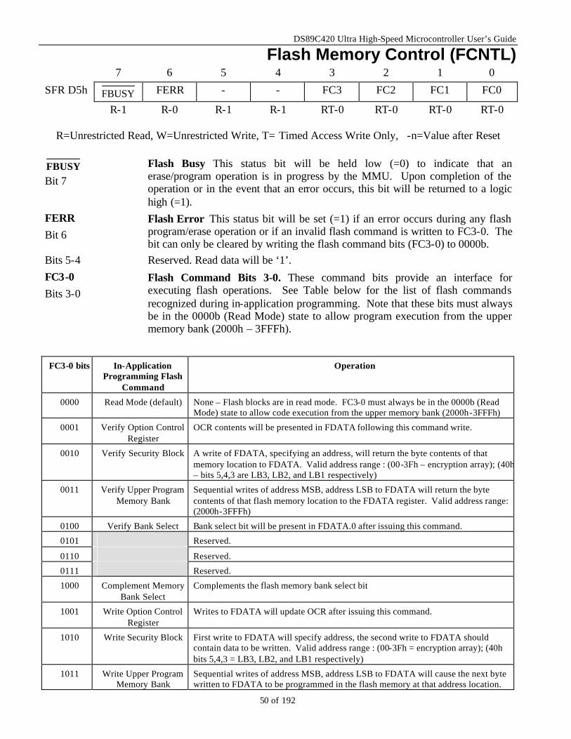
DS89C420 Ultra High-Speed Microcontroller User’s Guide
50 of 192
Flash Memory Control (FCNTL) 7 6 5 4 3 2 1 0
SFR D5h FBUSY FERR - - FC3 FC2 FC1 FC0
R-1 R-0 R-1 R-1 RT-0 RT-0 RT-0 RT-0
R=Unrestricted Read, W=Unrestricted Write, T= Timed Access Write Only, -n=Value after Reset
FBUSY Bit 7
Flash Busy This status bit will be held low (=0) to indicate that an erase/program operation is in progress by the MMU. Upon completion of the operation or in the event that an error occurs, this bit will be returned to a logic high (=1).
FERR Bit 6
Flash Error This status bit will be set (=1) if an error occurs during any flash program/erase operation or if an invalid flash command is written to FC3-0. The bit can only be cleared by writing the flash command bits (FC3-0) to 0000b.
Bits 5-4 Reserved. Read data will be ‘1’. FC3-0 Bits 3-0
Flash Command Bits 3-0. These command bits provide an interface for executing flash operations. See Table below for the list of flash commands recognized during in-application programming. Note that these bits must always be in the 0000b (Read Mode) state to allow program execution from the upper memory bank (2000h – 3FFFh).
FC3-0 bits In-Application Programming Flash
Command
Operation
0000 Read Mode (default) None – Flash blocks are in read mode. FC3-0 must always be in the 0000b (Read Mode) state to allow code execution from the upper memory bank (2000h-3FFFh)
0001 Verify Option Control Register
OCR contents will be presented in FDATA following this command write.
0010 Verify Security Block A write of FDATA, specifying an address, will return the byte contents of that memory location to FDATA. Valid address range : (00-3Fh – encryption array); (40h – bits 5,4,3 are LB3, LB2, and LB1 respectively)
0011 Verify Upper Program Memory Bank
Sequential writes of address MSB, address LSB to FDATA will return the byte contents of that flash memory location to the FDATA register. Valid address range: (2000h-3FFFh)
0100 Verify Bank Select Bank select bit will be present in FDATA.0 after issuing this command.
0101 Reserved.
0110 Reserved.
0111 Reserved.
1000 Complement Memory Bank Select
Complements the flash memory bank select bit
1001 Write Option Control Register
Writes to FDATA will update OCR after issuing this command.
1010 Write Security Block First write to FDATA will specify address, the second write to FDATA should contain data to be written. Valid address range : (00-3Fh = encryption array); (40h bits 5,4,3 = LB3, LB2, and LB1 respectively)
1011 Write Upper Program Memory Bank
Sequential writes of address MSB, address LSB to FDATA will cause the next byte written to FDATA to be programmed in the flash memory at that address location.
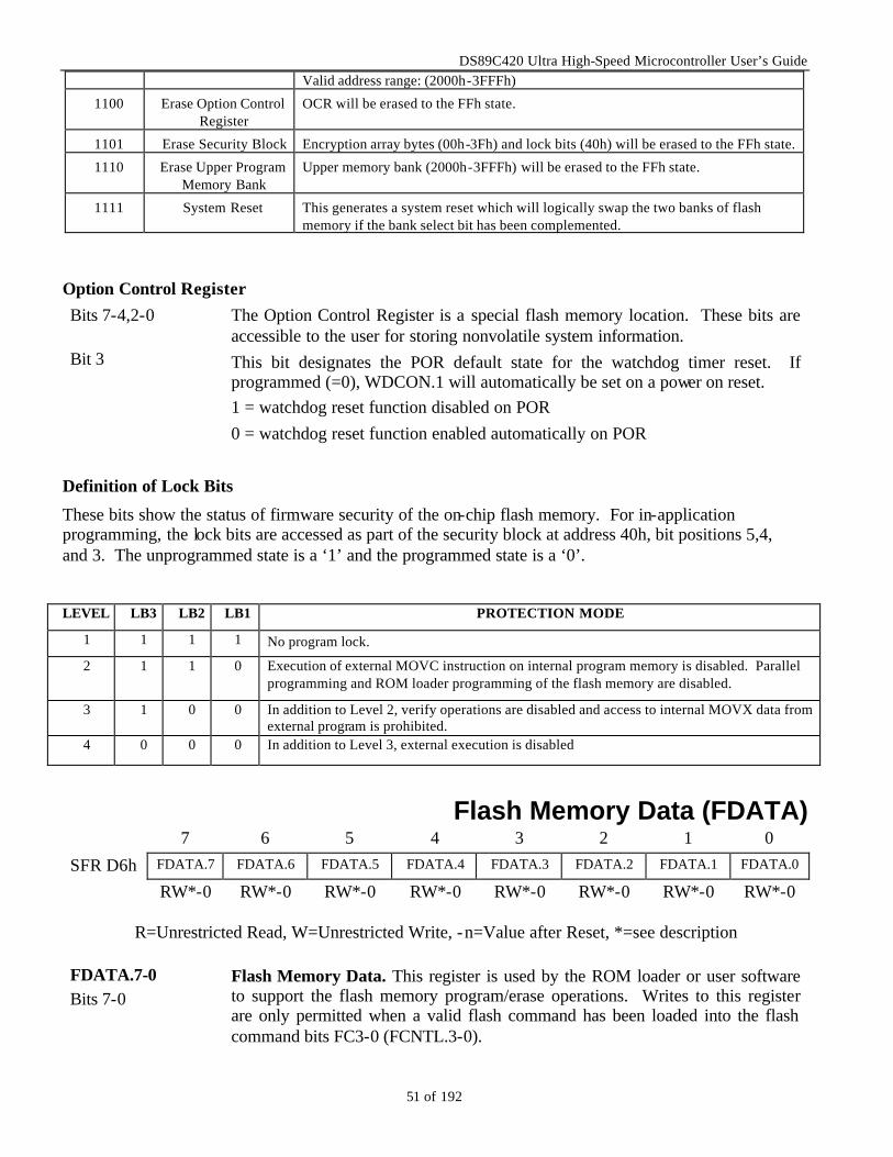
DS89C420 Ultra High-Speed Microcontroller User’s Guide
51 of 192
Valid address range: (2000h-3FFFh)
1100 Erase Option Control Register
OCR will be erased to the FFh state.
1101 Erase Security Block Encryption array bytes (00h-3Fh) and lock bits (40h) will be erased to the FFh state.
1110 Erase Upper Program Memory Bank
Upper memory bank (2000h-3FFFh) will be erased to the FFh state.
1111 System Reset This generates a system reset which will logically swap the two banks of flash memory if the bank select bit has been complemented.
Option Control Register Bits 7-4,2-0 The Option Control Register is a special flash memory location. These bits are
accessible to the user for storing nonvolatile system information. Bit 3 This bit designates the POR default state for the watchdog timer reset. If
programmed (=0), WDCON.1 will automatically be set on a power on reset. 1 = watchdog reset function disabled on POR 0 = watchdog reset function enabled automatically on POR
Definition of Lock Bits
These bits show the status of firmware security of the on-chip flash memory. For in-application programming, the lock bits are accessed as part of the security block at address 40h, bit positions 5,4, and 3. The unprogrammed state is a ‘1’ and the programmed state is a ‘0’.
LEVEL LB3 LB2 LB1 PROTECTION MODE
1 1 1 1 No program lock.
2 1 1 0 Execution of external MOVC instruction on internal program memory is disabled. Parallel programming and ROM loader programming of the flash memory are disabled.
3 1 0 0 In addition to Level 2, verify operations are disabled and access to internal MOVX data from external program is prohibited.
4 0 0 0 In addition to Level 3, external execution is disabled
Flash Memory Data (FDATA)
7 6 5 4 3 2 1 0
SFR D6h FDATA.7 FDATA.6 FDATA.5 FDATA.4 FDATA.3 FDATA.2 FDATA.1 FDATA.0 RW*-0 RW*-0 RW*-0 RW*-0 RW*-0 RW*-0 RW*-0 RW*-0
R=Unrestricted Read, W=Unrestricted Write, -n=Value after Reset, *=see description
FDATA.7-0 Bits 7-0
Flash Memory Data. This register is used by the ROM loader or user software to support the flash memory program/erase operations. Writes to this register are only permitted when a valid flash command has been loaded into the flash command bits FC3-0 (FCNTL.3-0).
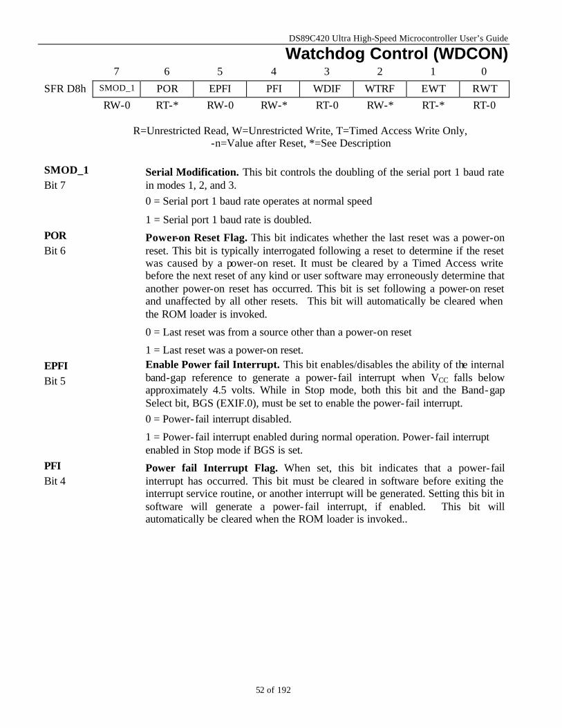
DS89C420 Ultra High-Speed Microcontroller User’s Guide
52 of 192
Watchdog Control (WDCON) 7 6 5 4 3 2 1 0
SFR D8h SMOD_1 POR EPFI PFI WDIF WTRF EWT RWT RW-0 RT-* RW-0 RW-* RT-0 RW-* RT-* RT-0
R=Unrestricted Read, W=Unrestricted Write, T=Timed Access Write Only,
-n=Value after Reset, *=See Description
SMOD_1 Bit 7
Serial Modification. This bit controls the doubling of the serial port 1 baud rate in modes 1, 2, and 3. 0 = Serial port 1 baud rate operates at normal speed
1 = Serial port 1 baud rate is doubled. POR Bit 6
Power-on Reset Flag. This bit indicates whether the last reset was a power-on reset. This bit is typically interrogated following a reset to determine if the reset was caused by a power-on reset. It must be cleared by a Timed Access write before the next reset of any kind or user software may erroneously determine that another power-on reset has occurred. This bit is set following a power-on reset and unaffected by all other resets. This bit will automatically be cleared when the ROM loader is invoked.
0 = Last reset was from a source other than a power-on reset
1 = Last reset was a power-on reset. EPFI Bit 5
Enable Power fail Interrupt. This bit enables/disables the ability of the internal band-gap reference to generate a power-fail interrupt when VCC falls below approximately 4.5 volts. While in Stop mode, both this bit and the Band-gap Select bit, BGS (EXIF.0), must be set to enable the power-fail interrupt. 0 = Power-fail interrupt disabled.
1 = Power-fail interrupt enabled during normal operation. Power-fail interrupt enabled in Stop mode if BGS is set.
PFI Bit 4
Power fail Interrupt Flag. When set, this bit indicates that a power-fail interrupt has occurred. This bit must be cleared in software before exiting the interrupt service routine, or another interrupt will be generated. Setting this bit in software will generate a power-fail interrupt, if enabled. This bit will automatically be cleared when the ROM loader is invoked..
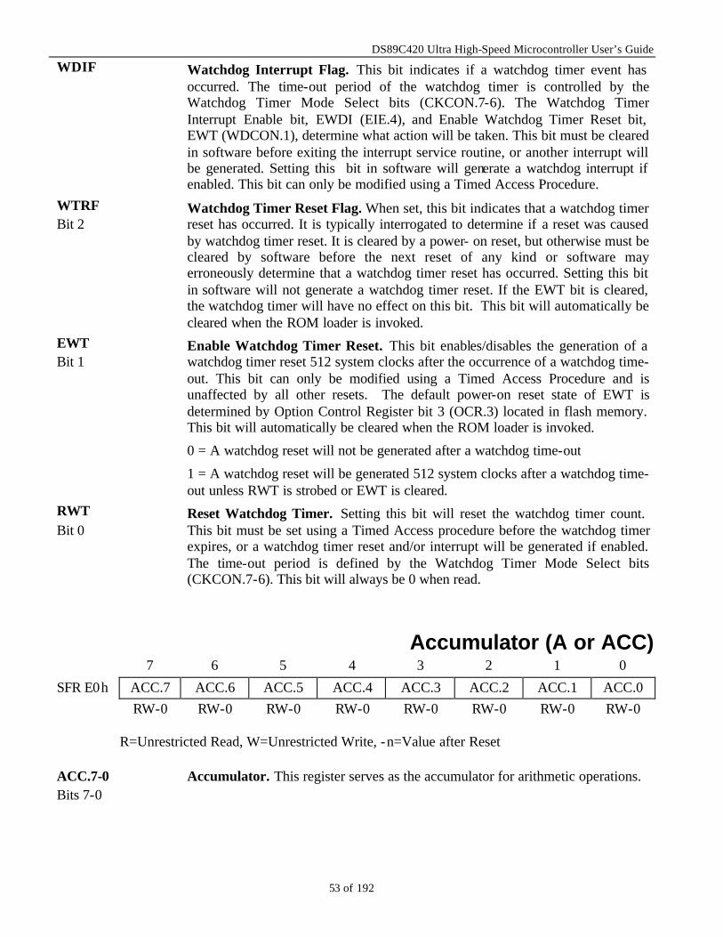
DS89C420 Ultra High-Speed Microcontroller User’s Guide
53 of 192
WDIF Watchdog Interrupt Flag. This bit indicates if a watchdog timer event has occurred. The time-out period of the watchdog timer is controlled by the Watchdog Timer Mode Select bits (CKCON.7-6). The Watchdog Timer Interrupt Enable bit, EWDI (EIE.4), and Enable Watchdog Timer Reset bit, EWT (WDCON.1), determine what action will be taken. This bit must be cleared in software before exiting the interrupt service routine, or another interrupt will be generated. Setting this bit in software will generate a watchdog interrupt if enabled. This bit can only be modified using a Timed Access Procedure.
WTRF Bit 2
Watchdog Timer Reset Flag. When set, this bit indicates that a watchdog timer reset has occurred. It is typically interrogated to determine if a reset was caused by watchdog timer reset. It is cleared by a power- on reset, but otherwise must be cleared by software before the next reset of any kind or software may erroneously determine that a watchdog timer reset has occurred. Setting this bit in software will not generate a watchdog timer reset. If the EWT bit is cleared, the watchdog timer will have no effect on this bit. This bit will automatically be cleared when the ROM loader is invoked.
EWT Bit 1
Enable Watchdog Timer Reset. This bit enables/disables the generation of a watchdog timer reset 512 system clocks after the occurrence of a watchdog time-out. This bit can only be modified using a Timed Access Procedure and is unaffected by all other resets. The default power-on reset state of EWT is determined by Option Control Register bit 3 (OCR.3) located in flash memory. This bit will automatically be cleared when the ROM loader is invoked.
0 = A watchdog reset will not be generated after a watchdog time-out
1 = A watchdog reset will be generated 512 system clocks after a watchdog time-out unless RWT is strobed or EWT is cleared.
RWT Bit 0
Reset Watchdog Timer. Setting this bit will reset the watchdog timer count. This bit must be set using a Timed Access procedure before the watchdog timer expires, or a watchdog timer reset and/or interrupt will be generated if enabled. The time-out period is defined by the Watchdog Timer Mode Select bits (CKCON.7-6). This bit will always be 0 when read.
Accumulator (A or ACC)
7 6 5 4 3 2 1 0
SFR E0h ACC.7 ACC.6 ACC.5 ACC.4 ACC.3 ACC.2 ACC.1 ACC.0 RW-0 RW-0 RW-0 RW-0 RW-0 RW-0 RW-0 RW-0
R=Unrestricted Read, W=Unrestricted Write, -n=Value after Reset
ACC.7-0 Bits 7-0
Accumulator. This register serves as the accumulator for arithmetic operations.
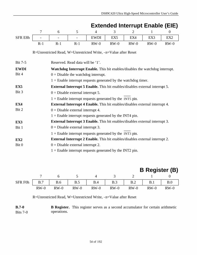
DS89C420 Ultra High-Speed Microcontroller User’s Guide
54 of 192
Extended Interrupt Enable (EIE)
7 6 5 4 3 2 1 0 SFR E8h - - - EWDI EX5 EX4 EX3 EX2 R-1 R-1 R-1 RW-0 RW-0 RW-0 RW-0 RW-0
R=Unrestricted Read, W=Unrestricted Write, -n=Value after Reset
Bit 7-5 Reserved. Read data will be ‘1’.
EWDI Bit 4
Watchdog Interrupt Enable. This bit enables/disables the watchdog interrupt. 0 = Disable the watchdog interrupt. 1 = Enable interrupt requests generated by the watchdog timer.
EX5 Bit 3
External Interrupt 5 Enable. This bit enables/disables external interrupt 5.
0 = Disable external interrupt 5.
1 = Enable interrupt requests generated by the INT5 pin. EX4 Bit 2
External Interrupt 4 Enable. This bit enables/disables external interrupt 4. 0 = Disable external interrupt 4. 1 = Enable interrupt requests generated by the INT4 pin.
EX3 Bit 1
External Interrupt 3 Enable. This bit enables/disables external interrupt 3. 0 = Disable external interrupt 3.
1 = Enable interrupt requests generated by the INT3 pin.
EX2 Bit 0
External Interrupt 2 Enable. This bit enables/disables external interrupt 2. 0 = Disable external interrupt 2. 1 = Enable interrupt requests generated by the INT2 pin.
B Register (B) 7 6 5 4 3 2 1 0
SFR F0h B.7 B.6 B.5 B.4 B.3 B.2 B.1 B.0 RW-0 RW-0 RW-0 RW-0 RW-0 RW-0 RW-0 RW-0
R=Unrestricted Read, W=Unrestricted Write, -n=Value after Reset
B.7-0 Bits 7-0
B Register. This register serves as a second accumulator for certain arithmetic operations.
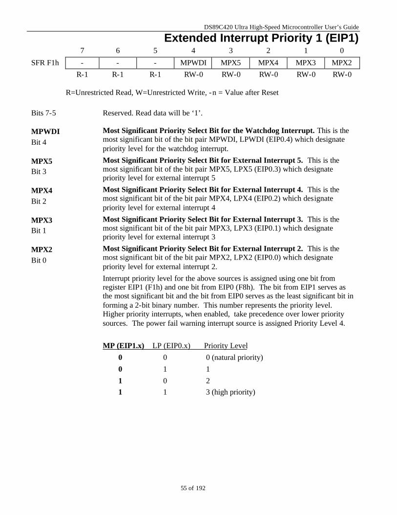
DS89C420 Ultra High-Speed Microcontroller User’s Guide
55 of 192
Extended Interrupt Priority 1 (EIP1) 7 6 5 4 3 2 1 0
SFR F1h - - - MPWDI MPX5 MPX4 MPX3 MPX2 R-1 R-1 R-1 RW-0 RW-0 RW-0 RW-0 RW-0
R=Unrestricted Read, W=Unrestricted Write, -n = Value after Reset
Bits 7-5 Reserved. Read data will be ‘1’.
MPWDI Bit 4
Most Significant Priority Select Bit for the Watchdog Interrupt. This is the most significant bit of the bit pair MPWDI, LPWDI (EIP0.4) which designate priority level for the watchdog interrupt.
MPX5 Bit 3
Most Significant Priority Select Bit for External Interrupt 5. This is the most significant bit of the bit pair MPX5, LPX5 (EIP0.3) which designate priority level for external interrupt 5
MPX4 Bit 2
Most Significant Priority Select Bit for External Interrupt 4. This is the most significant bit of the bit pair MPX4, LPX4 (EIP0.2) which designate priority level for external interrupt 4
MPX3 Bit 1
Most Significant Priority Select Bit for External Interrupt 3. This is the most significant bit of the bit pair MPX3, LPX3 (EIP0.1) which designate priority level for external interrupt 3
MPX2 Bit 0
Most Significant Priority Select Bit for External Interrupt 2. This is the most significant bit of the bit pair MPX2, LPX2 (EIP0.0) which designate priority level for external interrupt 2.
Interrupt priority level for the above sources is assigned using one bit from register EIP1 (F1h) and one bit from EIP0 (F8h). The bit from EIP1 serves as the most significant bit and the bit from EIP0 serves as the least significant bit in forming a 2-bit binary number. This number represents the priority level. Higher priority interrupts, when enabled, take precedence over lower priority sources. The power fail warning interrupt source is assigned Priority Level 4. MP (EIP1.x) LP (EIP0.x) Priority Level 0 0 0 (natural priority) 0 1 1 1 0 2 1 1 3 (high priority)
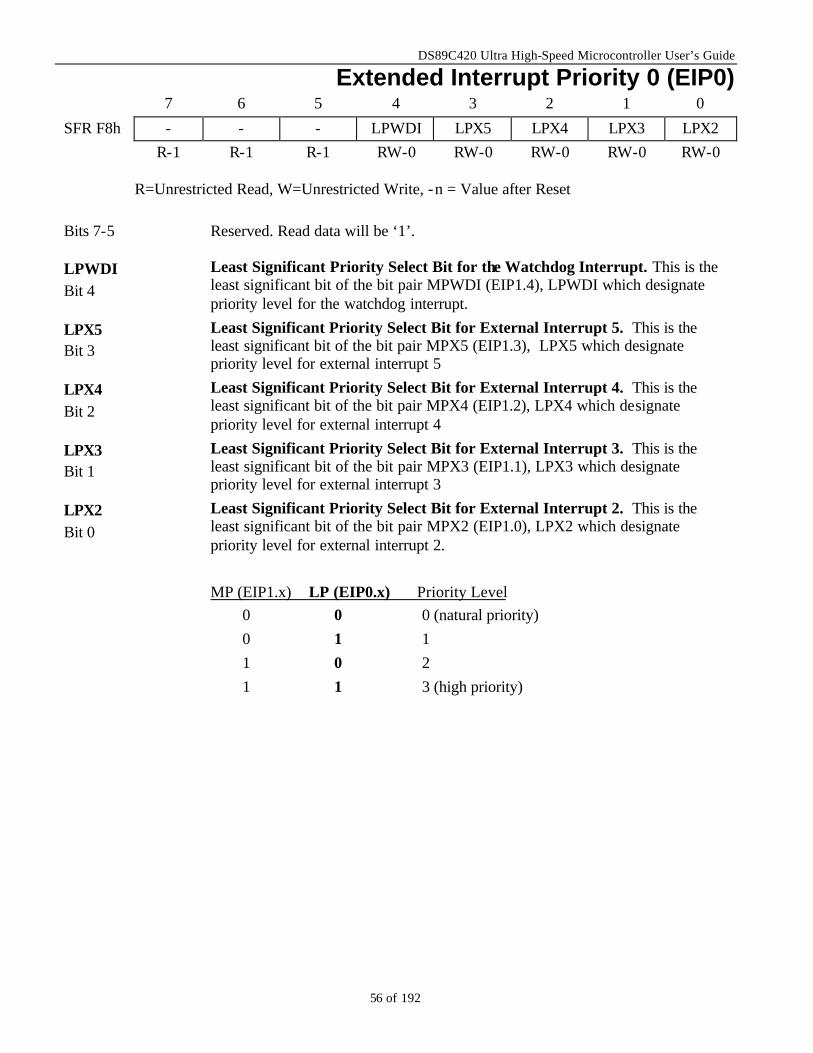
DS89C420 Ultra High-Speed Microcontroller User’s Guide
56 of 192
Extended Interrupt Priority 0 (EIP0) 7 6 5 4 3 2 1 0
SFR F8h - - - LPWDI LPX5 LPX4 LPX3 LPX2 R-1 R-1 R-1 RW-0 RW-0 RW-0 RW-0 RW-0
R=Unrestricted Read, W=Unrestricted Write, -n = Value after Reset
Bits 7-5 Reserved. Read data will be ‘1’.
LPWDI Bit 4
Least Significant Priority Select Bit for the Watchdog Interrupt. This is the least significant bit of the bit pair MPWDI (EIP1.4), LPWDI which designate priority level for the watchdog interrupt.
LPX5 Bit 3
Least Significant Priority Select Bit for External Interrupt 5. This is the least significant bit of the bit pair MPX5 (EIP1.3), LPX5 which designate priority level for external interrupt 5
LPX4 Bit 2
Least Significant Priority Select Bit for External Interrupt 4. This is the least significant bit of the bit pair MPX4 (EIP1.2), LPX4 which designate priority level for external interrupt 4
LPX3 Bit 1
Least Significant Priority Select Bit for External Interrupt 3. This is the least significant bit of the bit pair MPX3 (EIP1.1), LPX3 which designate priority level for external interrupt 3
LPX2 Bit 0
Least Significant Priority Select Bit for External Interrupt 2. This is the least significant bit of the bit pair MPX2 (EIP1.0), LPX2 which designate priority level for external interrupt 2.
MP (EIP1.x) LP (EIP0.x) Priority Level 0 0 0 (natural priority) 0 1 1 1 0 2 1 1 3 (high priority)
DS89C420 Ultra High-Speed Microcontroller User’s Guide
57 of 192
SECTION 5: CPU TIMING The timing of the Ultra High-Speed Microcontroller is the area with the greatest departure from the original 8051 series. This section will explain the timing and compare it to the original 8051.
OSCILLATOR The Ultra High-Speed Microcontroller provides an on-chip oscillator circuit that can be driven by an external crystal or by an off-chip TTL clock source. The oscillator circuit provides the internal clocking signals to the on-chip CPU and I/O circuits. In many designs, a crystal will be the preferred clock source. Figure 5-1 shows the required connections for a crystal and typical capacitor values. Some designs may prefer using an off-chip clock oscillator as the primary clock source. This configuration is illustrated in Figure 5-2. When using an off-chip oscillator, the duty cycle becomes important. As nearly as possible, a 50% duty cycle should be supplied.
XTAL1 This pin is the input to an inverting high gain amplifier. It also serves as the input for an off-chip oscillator. Note that when using an off-chip oscillator, XTAL2 is left unconnected.
XTAL2 This pin is the output of the crystal amplifier. It can be used to distribute the clock to other devices on the same board. If using a crystal, the loading on this pin should be kept to a minimum, especially capacitive loading.
OSCILLATOR CHARACTERISTICS The Ultra High-Speed Microcontroller was designed to operate with a parallel resonant AT cut crystal. The crystal should resonate at the desired frequency in its primary or fundamental mode. The oscillator employs a high gain amplifier to assure a clean waveform at high frequency. Due to the high performance nature of the product, both clock edges are used for internal timing. Therefore, the duty cycle of the clock source is of importance. A crystal circuit will balance itself automatically. Thus crystal users will not need to take extra precautions concerning duty cycle.
CRYSTAL SELECTION The Ultra High-Speed Microcontroller family was designed to operate with fundamental mode crystals for improved stability. Although most high speed (i.e., greater than 25 MHz) crystals operate from their third overtone, fundamental mode crystals are available from most major crystal suppliers. Designers are cautioned to ensure that high-speed crystals being specified for use in their application do operate at the rated frequency in their fundamental mode. The use of a third overtone crystal will typically result in oscillation rates at one-third the desired speed.
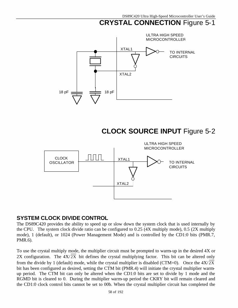
DS89C420 Ultra High-Speed Microcontroller User’s Guide
58 of 192
CRYSTAL CONNECTION Figure 5-1
CLOCK SOURCE INPUT Figure 5-2
SYSTEM CLOCK DIVIDE CONTROL The DS89C420 provides the ability to speed up or slow down the system clock that is used internally by the CPU. The system clock divide ratio can be configured to 0.25 (4X multiply mode), 0.5 (2X multiply mode), 1 (default), or 1024 (Power Management Mode) and is controlled by the CD1:0 bits (PMR.7, PMR.6). To use the crystal multiply mode, the multiplier circuit must be prompted to warm-up in the desired 4X or 2X configuration. The 4X/ X2 bit defines the crystal multiplying factor. This bit can be altered only from the divide by 1 (default) mode, while the crystal multiplier is disabled (CTM=0). Once the 4X/ X2 bit has been configured as desired, setting the CTM bit (PMR.4) will initiate the crystal multiplier warm-up period. The CTM bit can only be altered when the CD1:0 bits are set to divide by 1 mode and the RGMD bit is cleared to 0. During the multiplier warm-up period the CKRY bit will remain cleared and the CD1:0 clock control bits cannot be set to 00b. When the crystal multiplier circuit has completed the
TO INTERNAL CIRCUITS
XTAL1
XTAL2
ULTRA HIGH SPEED MICROCONTROLLER
18 pF 18 pF
TO INTERNAL CIRCUITS
XTAL1
XTAL2
ULTRA HIGH SPEED MICROCONTROLLER
CLOCK OSCILLATOR
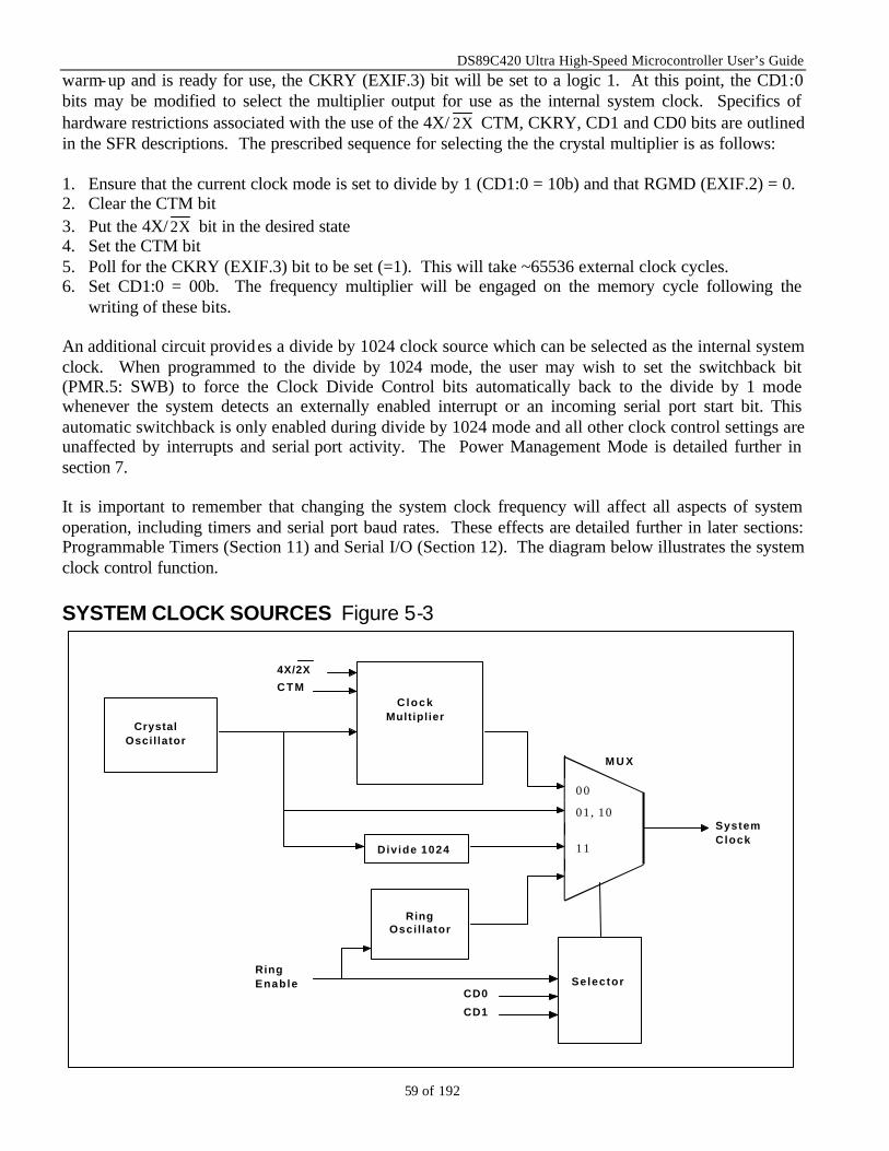
DS89C420 Ultra High-Speed Microcontroller User’s Guide
59 of 192
warm-up and is ready for use, the CKRY (EXIF.3) bit will be set to a logic 1. At this point, the CD1:0 bits may be modified to select the multiplier output for use as the internal system clock. Specifics of hardware restrictions associated with the use of the 4X/ X2 CTM, CKRY, CD1 and CD0 bits are outlined in the SFR descriptions. The prescribed sequence for selecting the the crystal multiplier is as follows: 1. Ensure that the current clock mode is set to divide by 1 (CD1:0 = 10b) and that RGMD (EXIF.2) = 0. 2. Clear the CTM bit 3. Put the 4X/ X2 bit in the desired state 4. Set the CTM bit 5. Poll for the CKRY (EXIF.3) bit to be set (=1). This will take ~65536 external clock cycles. 6. Set CD1:0 = 00b. The frequency multiplier will be engaged on the memory cycle following the
writing of these bits. An additional circuit provides a divide by 1024 clock source which can be selected as the internal system clock. When programmed to the divide by 1024 mode, the user may wish to set the switchback bit (PMR.5: SWB) to force the Clock Divide Control bits automatically back to the divide by 1 mode whenever the system detects an externally enabled interrupt or an incoming serial port start bit. This automatic switchback is only enabled during divide by 1024 mode and all other clock control settings are unaffected by interrupts and serial port activity. The Power Management Mode is detailed further in section 7. It is important to remember that changing the system clock frequency will affect all aspects of system operation, including timers and serial port baud rates. These effects are detailed further in later sections: Programmable Timers (Section 11) and Serial I/O (Section 12). The diagram below illustrates the system clock control function.
SYSTEM CLOCK SOURCES Figure 5-3
4X/2X
C T M
CrystalOscil lator
Div ide 1024
RingOsci l lator
C lockMultiplier
CD0
CD1
SelectorRingEnable
M U X
SystemClock
0 0
1 1
01, 10
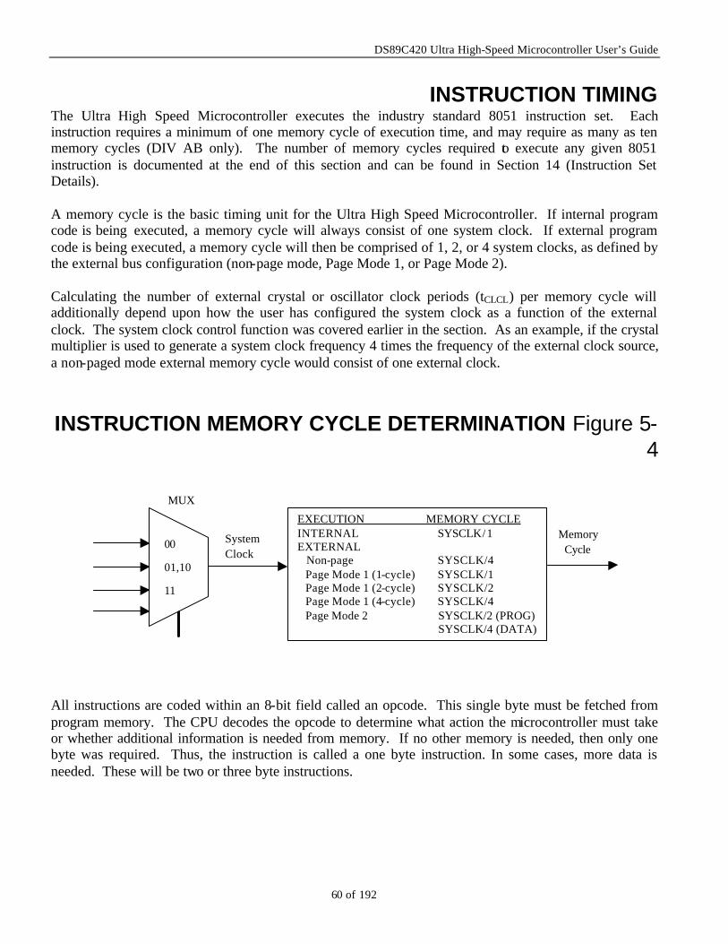
DS89C420 Ultra High-Speed Microcontroller User’s Guide
60 of 192
INSTRUCTION TIMING
The Ultra High Speed Microcontroller executes the industry standard 8051 instruction set. Each instruction requires a minimum of one memory cycle of execution time, and may require as many as ten memory cycles (DIV AB only). The number of memory cycles required to execute any given 8051 instruction is documented at the end of this section and can be found in Section 14 (Instruction Set Details). A memory cycle is the basic timing unit for the Ultra High Speed Microcontroller. If internal program code is being executed, a memory cycle will always consist of one system clock. If external program code is being executed, a memory cycle will then be comprised of 1, 2, or 4 system clocks, as defined by the external bus configuration (non-page mode, Page Mode 1, or Page Mode 2). Calculating the number of external crystal or oscillator clock periods (tCLCL) per memory cycle will additionally depend upon how the user has configured the system clock as a function of the external clock. The system clock control function was covered earlier in the section. As an example, if the crystal multiplier is used to generate a system clock frequency 4 times the frequency of the external clock source, a non-paged mode external memory cycle would consist of one external clock.
INSTRUCTION MEMORY CYCLE DETERMINATION Figure 5-
4
All instructions are coded within an 8-bit field called an opcode. This single byte must be fetched from program memory. The CPU decodes the opcode to determine what action the microcontroller must take or whether additional information is needed from memory. If no other memory is needed, then only one byte was required. Thus, the instruction is called a one byte instruction. In some cases, more data is needed. These will be two or three byte instructions.
System Clock
MUX
00
01,10
11
Memory Cycle
EXECUTION MEMORY CYCLE INTERNAL SYSCLK/1 EXTERNAL Non-page SYSCLK/4 Page Mode 1 (1-cycle) SYSCLK/1 Page Mode 1 (2-cycle) SYSCLK/2 Page Mode 1 (4-cycle) SYSCLK/4 Page Mode 2 SYSCLK/2 (PROG) SYSCLK/4 (DATA)
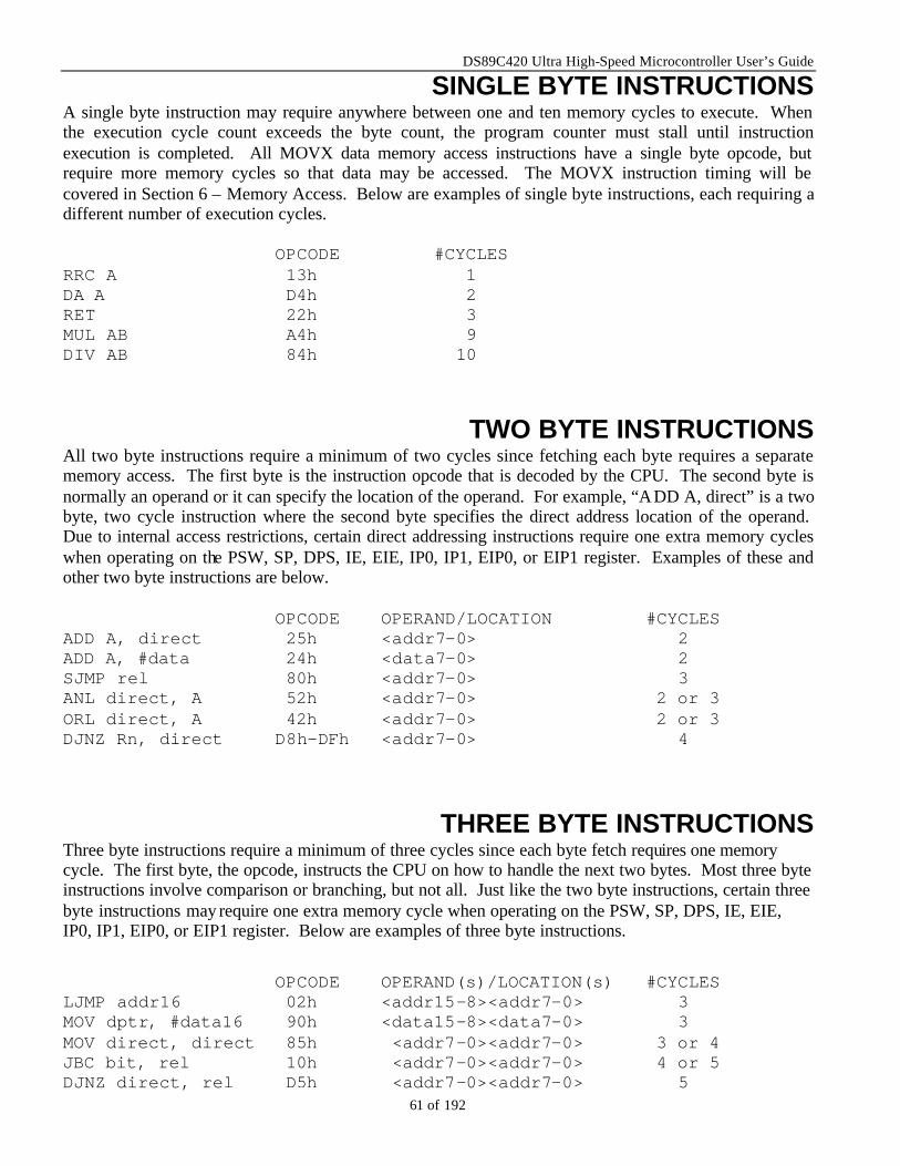
DS89C420 Ultra High-Speed Microcontroller User’s Guide
61 of 192
SINGLE BYTE INSTRUCTIONS A single byte instruction may require anywhere between one and ten memory cycles to execute. When the execution cycle count exceeds the byte count, the program counter must stall until instruction execution is completed. All MOVX data memory access instructions have a single byte opcode, but require more memory cycles so that data may be accessed. The MOVX instruction timing will be covered in Section 6 – Memory Access. Below are examples of single byte instructions, each requiring a different number of execution cycles.
OPCODE #CYCLES RRC A 13h 1 DA A D4h 2 RET 22h 3 MUL AB A4h 9 DIV AB 84h 10
TWO BYTE INSTRUCTIONS
All two byte instructions require a minimum of two cycles since fetching each byte requires a separate memory access. The first byte is the instruction opcode that is decoded by the CPU. The second byte is normally an operand or it can specify the location of the operand. For example, “ADD A, direct” is a two byte, two cycle instruction where the second byte specifies the direct address location of the operand. Due to internal access restrictions, certain direct addressing instructions require one extra memory cycles when operating on the PSW, SP, DPS, IE, EIE, IP0, IP1, EIP0, or EIP1 register. Examples of these and other two byte instructions are below. OPCODE OPERAND/LOCATION #CYCLES ADD A, direct 25h <addr7-0> 2 ADD A, #data 24h <data7-0> 2 SJMP rel 80h <addr7-0> 3 ANL direct, A 52h <addr7-0> 2 or 3 ORL direct, A 42h <addr7-0> 2 or 3 DJNZ Rn, direct D8h-DFh <addr7-0> 4
THREE BYTE INSTRUCTIONS Three byte instructions require a minimum of three cycles since each byte fetch requires one memory cycle. The first byte, the opcode, instructs the CPU on how to handle the next two bytes. Most three byte instructions involve comparison or branching, but not all. Just like the two byte instructions, certain three byte instructions may require one extra memory cycle when operating on the PSW, SP, DPS, IE, EIE, IP0, IP1, EIP0, or EIP1 register. Below are examples of three byte instructions.
OPCODE OPERAND(s)/LOCATION(s) #CYCLES LJMP addr16 02h <addr15-8><addr7-0> 3 MOV dptr, #data16 90h <data15-8><data7-0> 3 MOV direct, direct 85h <addr7-0><addr7-0> 3 or 4 JBC bit, rel 10h <addr7-0><addr7-0> 4 or 5 DJNZ direct, rel D5h <addr7-0><addr7-0> 5
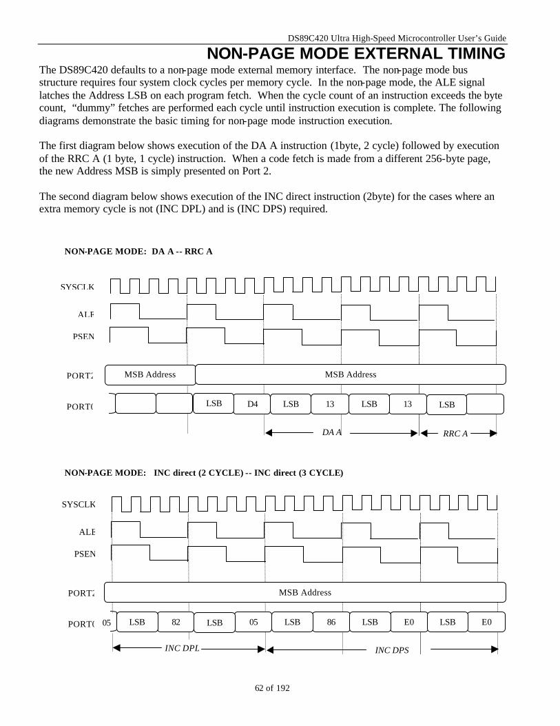
DS89C420 Ultra High-Speed Microcontroller User’s Guide
62 of 192
NON-PAGE MODE EXTERNAL TIMING The DS89C420 defaults to a non-page mode external memory interface. The non-page mode bus structure requires four system clock cycles per memory cycle. In the non-page mode, the ALE signal latches the Address LSB on each program fetch. When the cycle count of an instruction exceeds the byte count, “dummy” fetches are performed each cycle until instruction execution is complete. The following diagrams demonstrate the basic timing for non-page mode instruction execution. The first diagram below shows execution of the DA A instruction (1byte, 2 cycle) followed by execution of the RRC A (1 byte, 1 cycle) instruction. When a code fetch is made from a different 256-byte page, the new Address MSB is simply presented on Port 2. The second diagram below shows execution of the INC direct instruction (2byte) for the cases where an extra memory cycle is not (INC DPL) and is (INC DPS) required.
05
SYSCLK
ALE
PSEN
PORT2
PORT0 05 E0 82
INC DPL INC DPS
MSB Address
86 E0 LSB LSB LSB LSB LSB
NON-PAGE MODE: INC direct (2 CYCLE) -- INC direct (3 CYCLE)
SYSCLK
ALE
PSEN
PORT2
PORT0
MSB Address
D4
DA A
RRC A
13 13 LSB LSB LSB LSB
NON-PAGE MODE: DA A -- RRC A
MSB Address
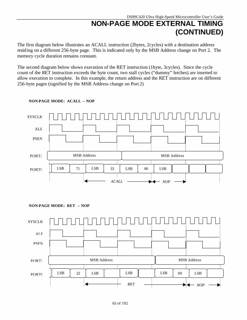
DS89C420 Ultra High-Speed Microcontroller User’s Guide
63 of 192
NON-PAGE MODE EXTERNAL TIMING (CONTINUED)
The first diagram below illustrates an ACALL instruction (2bytes, 2cycles) with a destination address residing on a different 256-byte page. This is indicated only by the MSB Address change on Port 2. The memory cycle duration remains constant. The second diagram below shows execution of the RET instruction (1byte, 3cycles). Since the cycle count of the RET instruction exceeds the byte count, two stall cycles (“dummy” fetches) are inserted to allow execution to complete. In this example, the return address and the RET instruction are on different 256-byte pages (signified by the MSB Address change on Port 2)
SYSCLK
ALE
PSEN
PORT2
PORT0
MSB Address
33 71
ACALL
MSB Address
LSB LSB LSB 00 LSB
NOP
NON-PAGE MODE: ACALL -- NOP
SYSCLK
ALE
PSEN
PORT2
PORT0 22 00
MSB Address
RET
LSB LSB LSB LSB LSB
NOP
NON-PAGE MODE: RET -- NOP
MSB Address
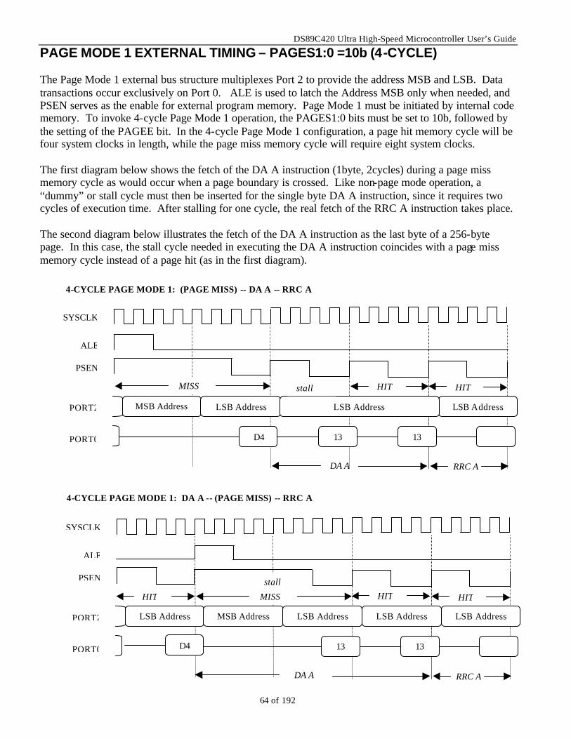
DS89C420 Ultra High-Speed Microcontroller User’s Guide
64 of 192
PAGE MODE 1 EXTERNAL TIMING – PAGES1:0 =10b (4-CYCLE) The Page Mode 1 external bus structure multiplexes Port 2 to provide the address MSB and LSB. Data transactions occur exclusively on Port 0. ALE is used to latch the Address MSB only when needed, and PSEN serves as the enable for external program memory. Page Mode 1 must be initiated by internal code memory. To invoke 4-cycle Page Mode 1 operation, the PAGES1:0 bits must be set to 10b, followed by the setting of the PAGEE bit. In the 4-cycle Page Mode 1 configuration, a page hit memory cycle will be four system clocks in length, while the page miss memory cycle will require eight system clocks. The first diagram below shows the fetch of the DA A instruction (1byte, 2cycles) during a page miss memory cycle as would occur when a page boundary is crossed. Like non-page mode operation, a “dummy” or stall cycle must then be inserted for the single byte DA A instruction, since it requires two cycles of execution time. After stalling for one cycle, the real fetch of the RRC A instruction takes place. The second diagram below illustrates the fetch of the DA A instruction as the last byte of a 256-byte page. In this case, the stall cycle needed in executing the DA A instruction coincides with a page miss memory cycle instead of a page hit (as in the first diagram).
SYSCLK
ALE
PSEN
PORT2
PORT0
MSB Address
LSB Address
D4
MISS HIT
DA A
LSB Address
HIT
RRC A
LSB Address
13 13
stall
4-CYCLE PAGE MODE 1: (PAGE MISS) -- DA A -- RRC A
HIT
SYSCLK
ALE
PSEN
PORT2
PORT0
LSB Address MSB Address
MISS HIT
stall
RRC A
HIT
D4
DA A
LSB Address LSB Address LSB Address
13 13
4-CYCLE PAGE MODE 1: DA A -- (PAGE MISS) -- RRC A
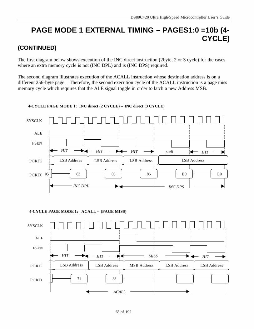
DS89C420 Ultra High-Speed Microcontroller User’s Guide
65 of 192
PAGE MODE 1 EXTERNAL TIMING – PAGES1:0 =10b (4-CYCLE)
(CONTINUED) The first diagram below shows execution of the INC direct instruction (2byte, 2 or 3 cycle) for the cases where an extra memory cycle is not (INC DPL) and is (INC DPS) required. The second diagram illustrates execution of the ACALL instruction whose destination address is on a different 256-byte page. Therefore, the second execution cycle of the ACALL instruction is a page miss memory cycle which requires that the ALE signal toggle in order to latch a new Address MSB.
stall
05
SYSCLK
ALE
PSEN
PORT2
PORT0
LSB Address
LSB Address
05
HIT HIT
E0 82
HIT HIT
INC DPL INC DPS
LSB Address
86 E0
LSB Address
4-CYCLE PAGE MODE 1: INC direct (2 CYCLE) -- INC direct (3 CYCLE)
SYSCLK
ALE
PSEN
PORT2
PORT0
LSB Address
LSB Address
33 71
HIT HIT
ACALL
LSB Address
MSB Address LSB Address
HIT MISS
4-CYCLE PAGE MODE 1: ACALL -- (PAGE MISS)
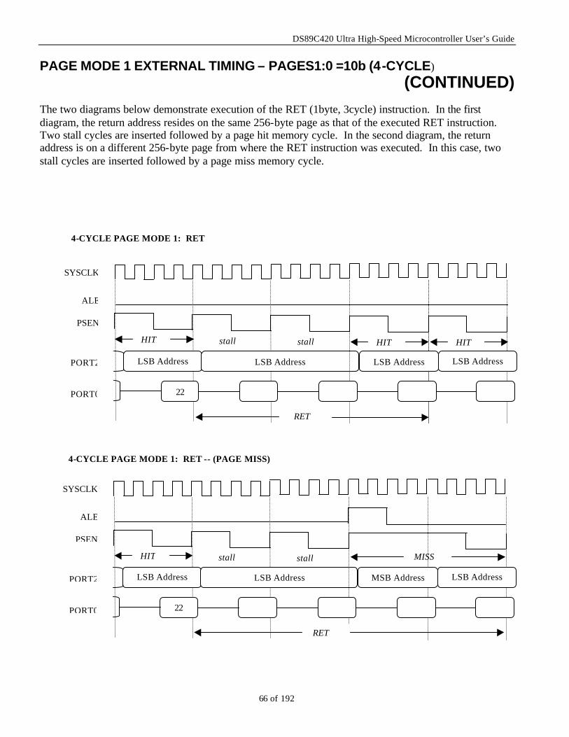
DS89C420 Ultra High-Speed Microcontroller User’s Guide
66 of 192
PAGE MODE 1 EXTERNAL TIMING – PAGES1:0 =10b (4-CYCLE)
(CONTINUED) The two diagrams below demonstrate execution of the RET (1byte, 3cycle) instruction. In the first diagram, the return address resides on the same 256-byte page as that of the executed RET instruction. Two stall cycles are inserted followed by a page hit memory cycle. In the second diagram, the return address is on a different 256-byte page from where the RET instruction was executed. In this case, two stall cycles are inserted followed by a page miss memory cycle.
SYSCLK
ALE
PSEN
PORT2
PORT0
LSB Address
LSB Address
stall
22
HIT stall
LSB Address
LSB Address
RET
HIT HIT
4-CYCLE PAGE MODE 1: RET
MISS
SYSCLK
ALE
PSEN
PORT2
PORT0
LSB Address
LSB Address
stall
22
HIT stall
MSB Address
LSB Address
RET
4-CYCLE PAGE MODE 1: RET -- (PAGE MISS)
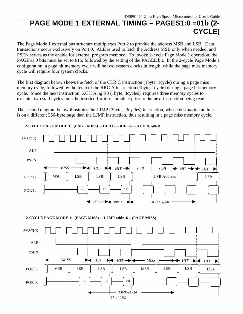
DS89C420 Ultra High-Speed Microcontroller User’s Guide
67 of 192
PAGE MODE 1 EXTERNAL TIMING – PAGES1:0 =01b (2-CYCLE)
The Page Mode 1 external bus structure multiplexes Port 2 to provide the address MSB and LSB. Data transactions occur exclusively on Port 0. ALE is used to latch the Address MSB only when needed, and PSEN serves as the enable for external program memory. To invoke 2-cycle Page Mode 1 operation, the PAGES1:0 bits must be set to 01b, followed by the setting of the PAGEE bit. In the 2-cycle Page Mode 1 configuration, a page hit memory cycle will be two system clocks in length, while the page miss memory cycle will require four system clocks. The first diagram below shows the fetch of the CLR C instruction (1byte, 1cycle) during a page miss memory cycle, followed by the fetch of the RRC A instruction (1byte, 1cycle) during a page hit memory cycle. Since the next instruction, XCH A, @R0 (1byte, 3cycles), requires three memory cycles to execute, two stall cycles must be inserted for it to complete prior to the next instruction being read. The second diagram below illustrates the LJMP (3bytes, 3cycles) instruction, whose destination address is on a different 256-byte page than the LJMP instruction, thus resulting in a page miss memory cycle.
SYSCLK
ALE
PSEN
PORT2
PORT0
MSB
LSB LSB LSB
C3 13 C6
MISS HIT HIT
CLR C RRC A
LSB Address
HIT
LSB
HIT
XCH A, @R0
stall stall
2-CYCLE PAGE MODE 1: (PAGE MISS) -- CLR C -- RRC A -- XCH A, @R0
SYSCLK
ALE
PSEN
PORT2
PORT0
MSB
LSB LSB LSB
02 50 00
MISS HIT HIT
LSB Address
MISS
LSB
HIT
LJMP addr16
MSB LSB
HIT
2-CYCLE PAGE MODE 1: (PAGE MISS) -- LJMP addr16 – (PAGE MISS)
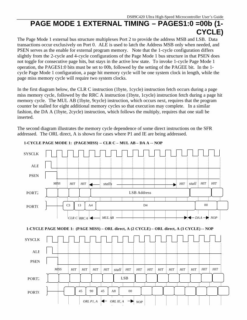
DS89C420 Ultra High-Speed Microcontroller User’s Guide
68 of 192
PAGE MODE 1 EXTERNAL TIMING – PAGES1:0 =00b (1-CYCLE)
The Page Mode 1 external bus structure multiplexes Port 2 to provide the address MSB and LSB. Data transactions occur exclusively on Port 0. ALE is used to latch the Address MSB only when needed, and PSEN serves as the enable for external program memory. Note that the 1-cycle configuration differs slightly from the 2-cycle and 4-cycle configurations of the Page Mode 1 bus structure in that PSEN does not toggle for consecutive page hits, but stays in the active low state. To invoke 1-cycle Page Mode 1 operation, the PAGES1:0 bits must be set to 00b, followed by the setting of the PAGEE bit. In the 1-cycle Page Mode 1 configuration, a page hit memory cycle will be one system clock in length, while the page miss memory cycle will require two system clocks. In the first diagram below, the CLR C instruction (1byte, 1cycle) instruction fetch occurs during a page miss memory cycle, followed by the RRC A instruction (1byte, 1cycle) instruction fetch during a page hit memory cycle. The MUL AB (1byte, 9cycle) instruction, which occurs next, requires that the program counter be stalled for eight additional memory cycles so that execut ion may complete. In a similar fashion, the DA A (1byte, 2cycle) instruction, which follows the multiply, requires that one stall be inserted. The second diagram illustrates the memory cycle dependence of some direct instructions on the SFR addressed. The ORL direct, A is shown for cases where P1 and IE are being addressed.
DA A
SYSCLK
ALE
PSEN
PORT2
PORT0
C3 13 A4
HIT
CLR C
HIT MISS
RRC A
MUL AB NOP
LSB Address
D4
00
HIT HIT HIT stall stalls
1-CYCLE PAGE MODE 1: (PAGE MISS) -- CLR C – MUL AB – DA A -- NOP
ORL P1, A
SYSCLK
ALE
PSEN
PORT2
PORT0
45 90
HIT HIT MISS
NOP
00
HIT HIT HIT
A8
ORL IE, A
45
LSB Address
stall HIT HIT HIT HIT HIT HIT HIT HIT
1-CYCLE PAGE MODE 1: (PAGE MISS) – ORL direct, A (2 CYCLE) – ORL direct, A (3 CYCLE) -- NOP
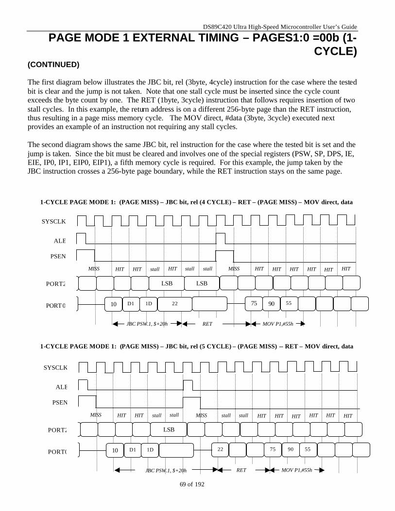
DS89C420 Ultra High-Speed Microcontroller User’s Guide
69 of 192
PAGE MODE 1 EXTERNAL TIMING – PAGES1:0 =00b (1-CYCLE)
(CONTINUED) The first diagram below illustrates the JBC bit, rel (3byte, 4cycle) instruction for the case where the tested bit is clear and the jump is not taken. Note that one stall cycle must be inserted since the cycle count exceeds the byte count by one. The RET (1byte, 3cycle) instruction that follows requires insertion of two stall cycles. In this example, the return address is on a different 256-byte page than the RET instruction, thus resulting in a page miss memory cycle. The MOV direct, #data (3byte, 3cycle) executed next provides an example of an instruction not requiring any stall cycles. The second diagram shows the same JBC bit, rel instruction for the case where the tested bit is set and the jump is taken. Since the bit must be cleared and involves one of the special registers (PSW, SP, DPS, IE, EIE, IP0, IP1, EIP0, EIP1), a fifth memory cycle is required. For this example, the jump taken by the JBC instruction crosses a 256-byte page boundary, while the RET instruction stays on the same page.
RET
SYSCLK
ALE
PSEN
PORT2
PORT 0
10 D1 1D
HIT HIT MISS
JBC PSW.1, $+20h
LSB
22
stall HIT HIT HIT stall stall
LSB
75
90 55
MISS
HIT HIT HIT HIT
MOV P1,#55h
1-CYCLE PAGE MODE 1: (PAGE MISS) – JBC bit, rel (4 CYCLE) – RET – (PAGE MISS) – MOV direct, data
SYSCLK
ALE
PSEN
PORT2
PORT0
10 D1 1D
HIT HIT MISS
JBC PSW.1, $+20h
LSB
stall HIT HIT HIT stall stall
22
75 90 55
MISS
HIT HIT HIT
MOV P1,#55h
stall
RET
1-CYCLE PAGE MODE 1: (PAGE MISS) – JBC bit, rel (5 CYCLE) – (PAGE MISS) -- RET – MOV direct, data
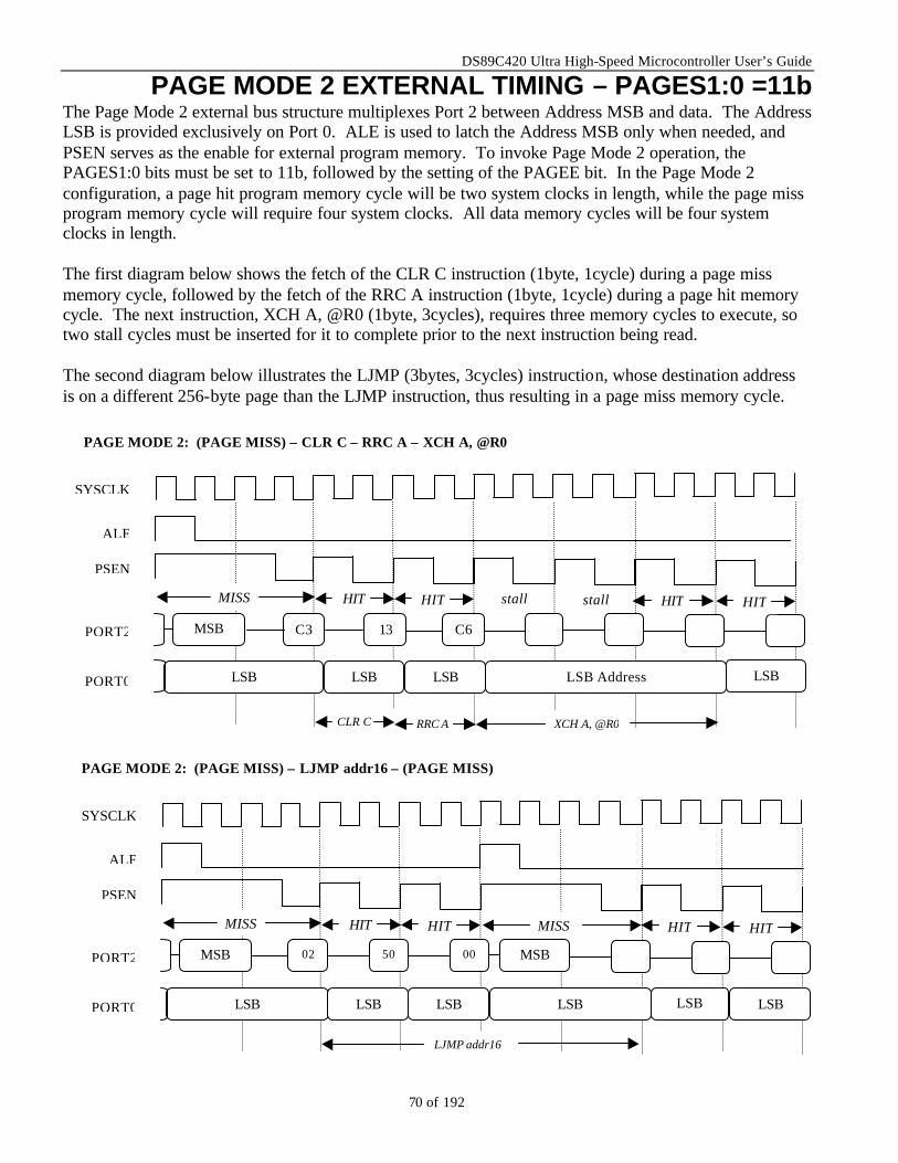
DS89C420 Ultra High-Speed Microcontroller User’s Guide
70 of 192
PAGE MODE 2 EXTERNAL TIMING – PAGES1:0 =11b The Page Mode 2 external bus structure multiplexes Port 2 between Address MSB and data. The Address LSB is provided exclusively on Port 0. ALE is used to latch the Address MSB only when needed, and PSEN serves as the enable for external program memory. To invoke Page Mode 2 operation, the PAGES1:0 bits must be set to 11b, followed by the setting of the PAGEE bit. In the Page Mode 2 configuration, a page hit program memory cycle will be two system clocks in length, while the page miss program memory cycle will require four system clocks. All data memory cycles will be four system clocks in length. The first diagram below shows the fetch of the CLR C instruction (1byte, 1cycle) during a page miss memory cycle, followed by the fetch of the RRC A instruction (1byte, 1cycle) during a page hit memory cycle. The next instruction, XCH A, @R0 (1byte, 3cycles), requires three memory cycles to execute, so two stall cycles must be inserted for it to complete prior to the next instruction being read. The second diagram below illustrates the LJMP (3bytes, 3cycles) instruction, whose destination address is on a different 256-byte page than the LJMP instruction, thus resulting in a page miss memory cycle.
SYSCLK
ALE
PSEN
PORT2
PORT0
MSB
LSB LSB LSB
02 50 00
MISS HIT HIT
LSB Address
MISS
LSB
HIT
LJMP addr16
LSB
HIT
MSB
PAGE MODE 2: (PAGE MISS) – LJMP addr16 – (PAGE MISS)
SYSCLK
ALE
PSEN
PORT2
PORT0
MSB
C3 13 C6
LSB LSB LSB
MISS HIT HIT
CLR C RRC A
LSB Address
HIT
LSB
HIT
XCH A, @R0
stall stall
PAGE MODE 2: (PAGE MISS) – CLR C – RRC A – XCH A, @R0
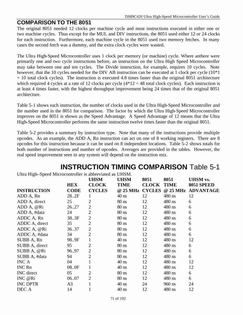
DS89C420 Ultra High-Speed Microcontroller User’s Guide
71 of 192
COMPARISON TO THE 8051 The original 8051 needed 12 clocks per machine cycle and most instructions executed in either one or two machine cycles. Thus except for the MUL and DIV instructions, the 8051 used either 12 or 24 clocks for each instruction. Furthermore, each machine cycle in the 8051 used two memory fetches. In many cases the second fetch was a dummy, and the extra clock cycles were wasted. The Ultra High-Speed Microcontroller uses 1 clock per memory (or machine) cycle. Where anthere were primarily one and two cycle instructions before, an instruction on the Ultra High Speed Microcontroller may take between one and ten cycles. The Divide instruction, for example, requires 10 cycles. Note however, that the 10 cycles needed for the DIV AB instruction can be executed at 1 clock per cycle (10*1 = 10 total clock cycles). The instruction is executed 4.8 times faster than the original 8051 architecture which required 4 cycles at a rate of 12 clocks per cycle (4*12 = 48 total clock cycles). Each instruction is at least 4 times faster, with the highest throughput improvement being 24 times that of the original 8051 architecture. Table 5-1 shows each instruction, the number of clocks used in the Ultra High-Speed Microcontroller and the number used in the 8051 for comparison. The factor by which the Ultra High-Speed Microcontroller improves on the 8051 is shown as the Speed Advantage. A Speed Advantage of 12 means that the Ultra High-Speed Microcontroller performs the same instruction twelve times faster than the original 8051. Table 5-2 provides a summary by instruction type. Note that many of the instructions provide multiple opcodes. As an example, the ADD A, Rn instruction can act on one of 8 working registers. There are 8 opcodes for this instruction because it can be used on 8 independent locations. Table 5-2 shows totals for both number of instructions and number of opcodes. Averages are provided in the tables. However, the real speed improvement seen in any system will depend on the instruction mix.
INSTRUCTION TIMING COMPARISON Table 5-1 Ultra High–Speed Microcontroller is abbreviated as UHSM. UHSM UHSM 8051 8051 UHSM vs. HEX CLOCK TIME CLOCK TIME 8051 SPEED INSTRUCTION CODE CYCLES @ 25 MHz CYCLES @ 25 MHz ADVANTAGE ADD A, Rn 28..2F 1 40 ns 12 480 ns 12 ADD A, direct 25 2 80 ns 12 480 ns 6 ADD A, @Ri 26..27 2 80 ns 12 480 ns 6 ADD A, #data 24 2 80 ns 12 480 ns 6 ADDC A, Rn 38..3F 2 80 ns 12 480 ns 6 ADDC A, direct 35 2 80 ns 12 480 ns 6 ADDC A, @Ri 36..37 2 80 ns 12 480 ns 6 ADDC A, #data 34 2 80 ns 12 480 ns 6 SUBB A, Rn 98..9F 1 40 ns 12 480 ns 12 SUBB A, direct 95 2 80 ns 12 480 ns 6 SUBB A, @Ri 96..97 2 80 ns 12 480 ns 6 SUBB A, #data 94 2 80 ns 12 480 ns 6 INC A 04 1 40 ns 12 480 ns 12 INC Rn 08..0F 1 40 ns 12 480 ns 12 INC direct 05 2 80 ns 12 480 ns 6 INC @Ri 06..07 2 80 ns 12 480 ns 6 INC DPTR A3 1 40 ns 24 960 ns 24 DEC A 14 1 40 ns 12 480 ns 12
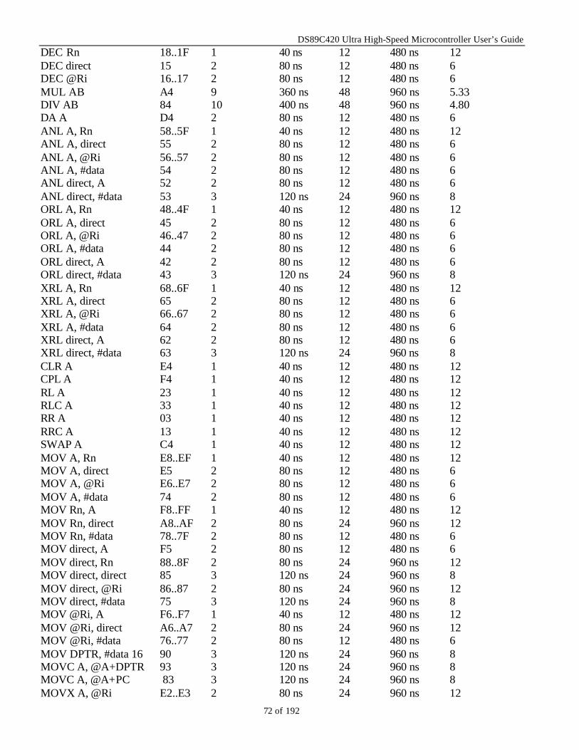
DS89C420 Ultra High-Speed Microcontroller User’s Guide
72 of 192
DEC Rn 18..1F 1 40 ns 12 480 ns 12 DEC direct 15 2 80 ns 12 480 ns 6 DEC @Ri 16..17 2 80 ns 12 480 ns 6 MUL AB A4 9 360 ns 48 960 ns 5.33 DIV AB 84 10 400 ns 48 960 ns 4.80 DA A D4 2 80 ns 12 480 ns 6 ANL A, Rn 58..5F 1 40 ns 12 480 ns 12 ANL A, direct 55 2 80 ns 12 480 ns 6 ANL A, @Ri 56..57 2 80 ns 12 480 ns 6 ANL A, #data 54 2 80 ns 12 480 ns 6 ANL direct, A 52 2 80 ns 12 480 ns 6 ANL direct, #data 53 3 120 ns 24 960 ns 8 ORL A, Rn 48..4F 1 40 ns 12 480 ns 12 ORL A, direct 45 2 80 ns 12 480 ns 6 ORL A, @Ri 46..47 2 80 ns 12 480 ns 6 ORL A, #data 44 2 80 ns 12 480 ns 6 ORL direct, A 42 2 80 ns 12 480 ns 6 ORL direct, #data 43 3 120 ns 24 960 ns 8 XRL A, Rn 68..6F 1 40 ns 12 480 ns 12 XRL A, direct 65 2 80 ns 12 480 ns 6 XRL A, @Ri 66..67 2 80 ns 12 480 ns 6 XRL A, #data 64 2 80 ns 12 480 ns 6 XRL direct, A 62 2 80 ns 12 480 ns 6 XRL direct, #data 63 3 120 ns 24 960 ns 8 CLR A E4 1 40 ns 12 480 ns 12 CPL A F4 1 40 ns 12 480 ns 12 RL A 23 1 40 ns 12 480 ns 12 RLC A 33 1 40 ns 12 480 ns 12 RR A 03 1 40 ns 12 480 ns 12 RRC A 13 1 40 ns 12 480 ns 12 SWAP A C4 1 40 ns 12 480 ns 12 MOV A, Rn E8..EF 1 40 ns 12 480 ns 12 MOV A, direct E5 2 80 ns 12 480 ns 6 MOV A, @Ri E6..E7 2 80 ns 12 480 ns 6 MOV A, #data 74 2 80 ns 12 480 ns 6 MOV Rn, A F8..FF 1 40 ns 12 480 ns 12 MOV Rn, direct A8..AF 2 80 ns 24 960 ns 12 MOV Rn, #data 78..7F 2 80 ns 12 480 ns 6 MOV direct, A F5 2 80 ns 12 480 ns 6 MOV direct, Rn 88..8F 2 80 ns 24 960 ns 12 MOV direct, direct 85 3 120 ns 24 960 ns 8 MOV direct, @Ri 86..87 2 80 ns 24 960 ns 12 MOV direct, #data 75 3 120 ns 24 960 ns 8 MOV @Ri, A F6..F7 1 40 ns 12 480 ns 12 MOV @Ri, direct A6..A7 2 80 ns 24 960 ns 12 MOV @Ri, #data 76..77 2 80 ns 12 480 ns 6 MOV DPTR, #data 16 90 3 120 ns 24 960 ns 8 MOVC A, @A+DPTR 93 3 120 ns 24 960 ns 8 MOVC A, @A+PC 83 3 120 ns 24 960 ns 8 MOVX A, @Ri E2..E3 2 80 ns 24 960 ns 12
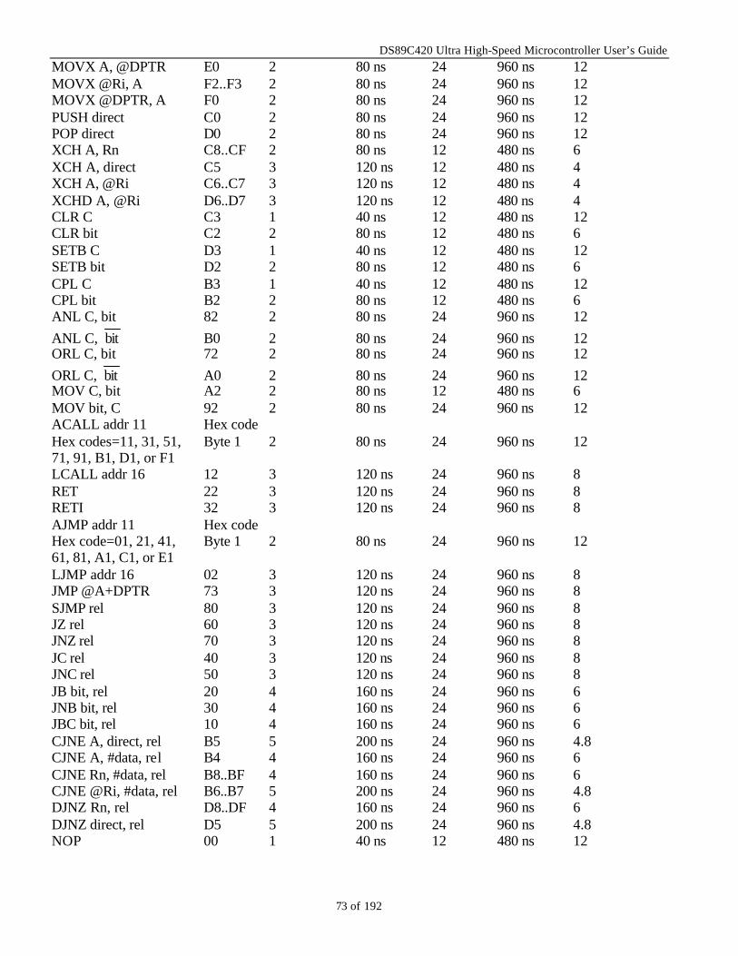
DS89C420 Ultra High-Speed Microcontroller User’s Guide
73 of 192
MOVX A, @DPTR E0 2 80 ns 24 960 ns 12 MOVX @Ri, A F2..F3 2 80 ns 24 960 ns 12 MOVX @DPTR, A F0 2 80 ns 24 960 ns 12 PUSH direct C0 2 80 ns 24 960 ns 12 POP direct D0 2 80 ns 24 960 ns 12 XCH A, Rn C8..CF 2 80 ns 12 480 ns 6 XCH A, direct C5 3 120 ns 12 480 ns 4 XCH A, @Ri C6..C7 3 120 ns 12 480 ns 4 XCHD A, @Ri D6..D7 3 120 ns 12 480 ns 4 CLR C C3 1 40 ns 12 480 ns 12 CLR bit C2 2 80 ns 12 480 ns 6 SETB C D3 1 40 ns 12 480 ns 12 SETB bit D2 2 80 ns 12 480 ns 6 CPL C B3 1 40 ns 12 480 ns 12 CPL bit B2 2 80 ns 12 480 ns 6 ANL C, bit 82 2 80 ns 24 960 ns 12 ANL C, bit B0 2 80 ns 24 960 ns 12 ORL C, bit 72 2 80 ns 24 960 ns 12 ORL C, bit A0 2 80 ns 24 960 ns 12 MOV C, bit A2 2 80 ns 12 480 ns 6 MOV bit, C 92 2 80 ns 24 960 ns 12 ACALL addr 11 Hex code Hex codes=11, 31, 51, Byte 1 2 80 ns 24 960 ns 12 71, 91, B1, D1, or F1 LCALL addr 16 12 3 120 ns 24 960 ns 8 RET 22 3 120 ns 24 960 ns 8 RETI 32 3 120 ns 24 960 ns 8 AJMP addr 11 Hex code Hex code=01, 21, 41, Byte 1 2 80 ns 24 960 ns 12 61, 81, A1, C1, or E1 LJMP addr 16 02 3 120 ns 24 960 ns 8 JMP @A+DPTR 73 3 120 ns 24 960 ns 8 SJMP rel 80 3 120 ns 24 960 ns 8 JZ rel 60 3 120 ns 24 960 ns 8 JNZ rel 70 3 120 ns 24 960 ns 8 JC rel 40 3 120 ns 24 960 ns 8 JNC rel 50 3 120 ns 24 960 ns 8 JB bit, rel 20 4 160 ns 24 960 ns 6 JNB bit, rel 30 4 160 ns 24 960 ns 6 JBC bit, rel 10 4 160 ns 24 960 ns 6 CJNE A, direct, rel B5 5 200 ns 24 960 ns 4.8 CJNE A, #data, rel B4 4 160 ns 24 960 ns 6 CJNE Rn, #data, rel B8..BF 4 160 ns 24 960 ns 6 CJNE @Ri, #data, rel B6..B7 5 200 ns 24 960 ns 4.8 DJNZ Rn, rel D8..DF 4 160 ns 24 960 ns 6 DJNZ direct, rel D5 5 200 ns 24 960 ns 4.8 NOP 00 1 40 ns 12 480 ns 12
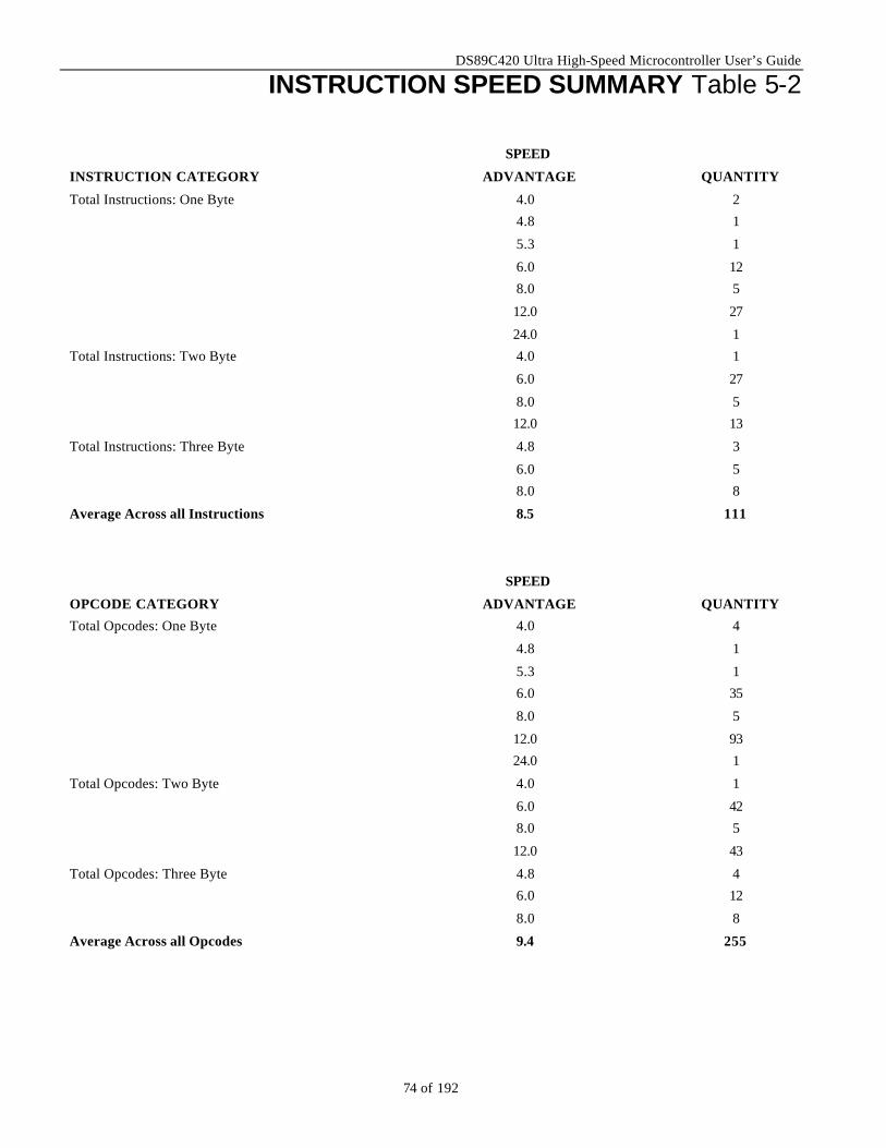
DS89C420 Ultra High-Speed Microcontroller User’s Guide
74 of 192
INSTRUCTION SPEED SUMMARY Table 5-2
INSTRUCTION CATEGORY
SPEED
ADVANTAGE
QUANTITY
Total Instructions: One Byte 4.0 2
4.8 1
5.3 1
6.0 12
8.0 5
12.0 27
24.0 1
Total Instructions: Two Byte 4.0 1
6.0 27
8.0 5
12.0 13
Total Instructions: Three Byte 4.8 3
6.0 5
8.0 8
Average Across all Instructions 8.5 111
OPCODE CATEGORY
SPEED
ADVANTAGE
QUANTITY
Total Opcodes: One Byte 4.0 4
4.8 1
5.3 1
6.0 35
8.0 5
12.0 93
24.0 1
Total Opcodes: Two Byte 4.0 1
6.0 42
8.0 5
12.0 43
Total Opcodes: Three Byte 4.8 4
6.0 12
8.0 8
Average Across all Opcodes 9.4 255
DS89C420 Ultra High-Speed Microcontroller User’s Guide
75 of 192
SECTION 6: MEMORY ACCESS The DS89C420 Ultra High-Speed Microcontroller supports the memory interface convention established for the industry standard 80C51, but also implements two new page mode memory interfaces needed to support ultra high-speed external operation. These external page mode interfaces will be described later in this section. Program and data memory areas can be implemented on-chip, off-chip, or as a combination. When opting not to use the internal memory provided, or when exceeding the maximum address of on-chip program or data memory, the device will perform an external memory access using the Expanded memory bus on ports 0 and 2. While serving as a memory bus, port 0 and port 2 cannot function as I/O ports. The PSEN signal will be driven active low to function as a chip enable or output enable when performing external code memory fetches. The RD and WR signals serve as enables when accessing external SRAM data memory. Program execution always begins at the reset vector, address 0000h. If on-chip program memory is enabled, program execution will begin at internal location 0000h, otherwise external program memory will be used. Any reset will cause the next program fetch to begin at this location. Subsequent branches and interrupts determine how program memory fetches deviate from sequential addressing.
INTERNAL FLASH MEMORY The DS89C420 Ultra High-Speed Microcontroller contains five physically distinct blocks of embedded flash memory. The two largest blocks, each 8KB, provide a total of 16KB for use as internal program memory. A 64 byte flash Security Block has been incorporated to allow encryption during program memory verify operations. To further protect internal code against undesirable access, a three- level lock system has been implemented in a separate flash memory block. This single byte block contains three lock bits (LB1, LB2, LB3), each of which can individually enable higher lock levels and greater code protection. The fifth flash memory block resident to the DS89C420 is the Option Control Register. This byte contains a bit to enable or disable the watchdog timer reset function (EWT=WDCON.1) on a power-on reset. The two 8KB program memory blocks form a contiguous 16KB address range extending from 0000h through 3FFFh. The on-chip decoded address range is controlled in hardware by the EA pin, and in software through the ROMSIZE feature. The EA pin enables or disables the ability to access internal program memory and overrides any software configured bit settings. The logic state of the EA pin should only be changed when the microcontroller is being held in reset. The EA pin is sampled on each exit from the reset state to determine whether program fetching should begin internally or externally. Whe n the EA pin is low, all code fetches are done externally via the Expanded bus. When the EA pin is high, code fetches begin from internal program memory. Code fetches exceeding the maximum address of on-chip program memory cause the device to access off-chip program memory. The maximum on-chip decoded address is selectable by software using the ROMSIZE feature. ROMSIZE FEATURE Using the ROMSIZE feature, software can allow the DS89C420 to behave like a device with le ss on-chip memory. The maximum memory size is dynamically variable. Thus, a portion of memory can be removed from the memory map to access off-chip memory, then restored to access on-chip memory. In fact, all of the on-chip memory can be removed from the memory map allowing the full 64KB external memory space to be addressed.
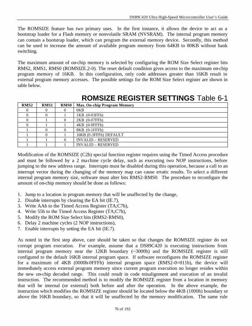
DS89C420 Ultra High-Speed Microcontroller User’s Guide
76 of 192
The ROMSIZE feature has two primary uses. In the first instance, it allows the device to act as a bootstrap loader for a Flash memory or nonvolatile SRAM (NVSRAM). The internal program memory can contain a bootstrap loader, which can program the external memory device. Secondly, this method can be used to increase the amount of available program memory from 64KB to 80KB without bank switching. The maximum amount of on-chip memory is selected by configuring the ROM Size Select register bits RMS2, RMS1, RMS0 (ROMSIZE.2-0). The reset default condition gives access to the maximum on-chip program memory of 16KB. In this configuration, only code addresses greater than 16KB result in external program memory accesses. The possible settings for the ROM Size Select register are shown in table below.
ROMSIZE REGISTER SETTINGS Table 6-1 RMS2 RMS1 RMS0 Max. On-chip Program Memory
0 0 0 0KB 0 0 1 1KB (0-03FFh) 0 1 0 2KB (0-07FFh) 0 1 1 4KB (0-0FFFh) 1 0 0 8KB (0-1FFFh) 1 0 1 16KB (0-3FFFh) DEFAULT 1 1 0 INVALID – RESERVED 1 1 1 INVALID – RESERVED
Modification of the ROMSIZE (C2h) special function register requires using the Timed Access procedure and must be followed by a 2 machine cycle delay, such as executing two NOP instructions, before jumping to the new address range. Interrupts must be disabled during this operation, because a call to an interrupt vector during the changing of the memory map can cause erratic results. To select a different internal program memory size, software must alter bits RMS2-RMS0. The procedure to reconfigure the amount of on-chip memory should be done as follows: 1. Jump to a location in program memory that will be unaffected by the change, 2. Disable interrupts by clearing the EA bit (IE.7), 3. Write AAh to the Timed Access Register (TA;C7h), 4. Write 55h to the Timed Access Register (TA;C7h), 5. Modify the ROM Size Select bits (RMS2-RMS0), 6. Delay 2 machine cycles (2 NOP instructions), 7. Enable interrupts by setting the EA bit (IE.7). As noted in the first step above, care should be taken so that changes the ROMSIZE register do not corrupt program execution. For example, assume that a DS89C420 is executing instructions from internal program memory near the 12KB boundary (~3000h) and the ROMSIZE register is still configured to the default 16KB internal program space. If software reconfigures the ROMSIZE register for a maximum of 4KB (0000h-0FFFh) internal program space (RMS2-0=011b), the device will immediately access external program memory since current program execution no longer resides within the new on-chip decoded range. This could result in code misalignment and execution of an invalid instruction. The recommended method is to modify the ROMSIZE register from a location in memory that will be internal (or external) both before and after the operation. In the above example, the instruction which modifies the ROMSIZE register should be located below the 4KB (1000h) boundary or above the 16KB boundary, so that it will be unaffected by the memory modification. The same rule
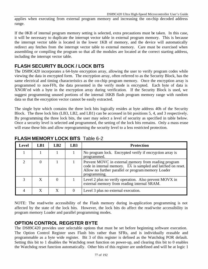
DS89C420 Ultra High-Speed Microcontroller User’s Guide
77 of 192
applies when executing from external program memory and increasing the on-chip decoded address range. If the 0KB of internal program memory setting is selected, extra precautions must be taken. In this case, it will be necessary to duplicate the interrupt vector table in external program memory. This is because the interrupt vector table is located in the lower 1KB of memory, and the device will automatically redirect any fetches from the interrupt vector table to external memory. Care must be exercised when assembling or compiling the program so that all the modules are located at the correct starting address, including the interrupt vector table. FLASH SECURITY BLOCK / LOCK BITS The DS89C420 incorporates a 64-byte encryption array, allowing the user to verify program codes while viewing the data in encrypted form. The encryption array, often referred to as the Security Block, has the same electrical and timing characteristics as the on-chip program memory. Once the encryption array is programmed to non-FFh, the data presented in the verify mode is encrypted. Each byte of data is XNOR’ed with a byte in the encryption array during verification. If the Security Block is used, we suggest programming unused portions of the internal 16KB flash program memory range with random data so that the encryption vector cannot be easily extracted. The single byte which contains the three lock bits logically resides at byte address 40h of the Security Block. The three lock bits (LB3, LB2, and LB1) can be accessed in bit positions 5, 4, and 3 respectively. By programming the three lock bits, the user may select a level of security as specified in table below. Once a security level is selected and programmed, the setting of the lock bits remains. Only a mass erase will erase these bits and allow reprogramming the security level to a less restricted protection.
FLASH MEMORY LOCK BITS Table 6-2 Level LB1 LB2 LB3 Protection
1 1 1 1 No program lock. Encrypted verify if encryp tion array is programmed.
2 0 1 1 Prevent MOVC in external memory from reading program code in internal memory. EA is sampled and latched on reset. Allow no further parallel or program memory Loader programming.
3 X 0 1 Level 2 plus no verify operation. Also prevent MOVX in external memory from reading internal SRAM.
4 X X 0 Level 3 plus no external execution.
NOTE: The read/write accessibility of the Flash memory during in-application programming is not affected by the state of the lock bits. However, the lock bits do affect the read/write accessibility in program memory Loader and parallel programming modes. OPTION CONTROL REGISTER BYTE The DS89C420 provides user selectable options that must be set before beginning software execution. The Option Control Register uses Flash bits rather than SFRs, and is individually erasable and programmable as a byte wide register. Bit 3 of this register is defined as the Watchdog POR default. Setting this bit to 1 disables the Watchdog reset function on power-up, and clearing this bit to 0 enables the Watchdog reset function automatically. Other bits of this register are undefined and will be at logic 1
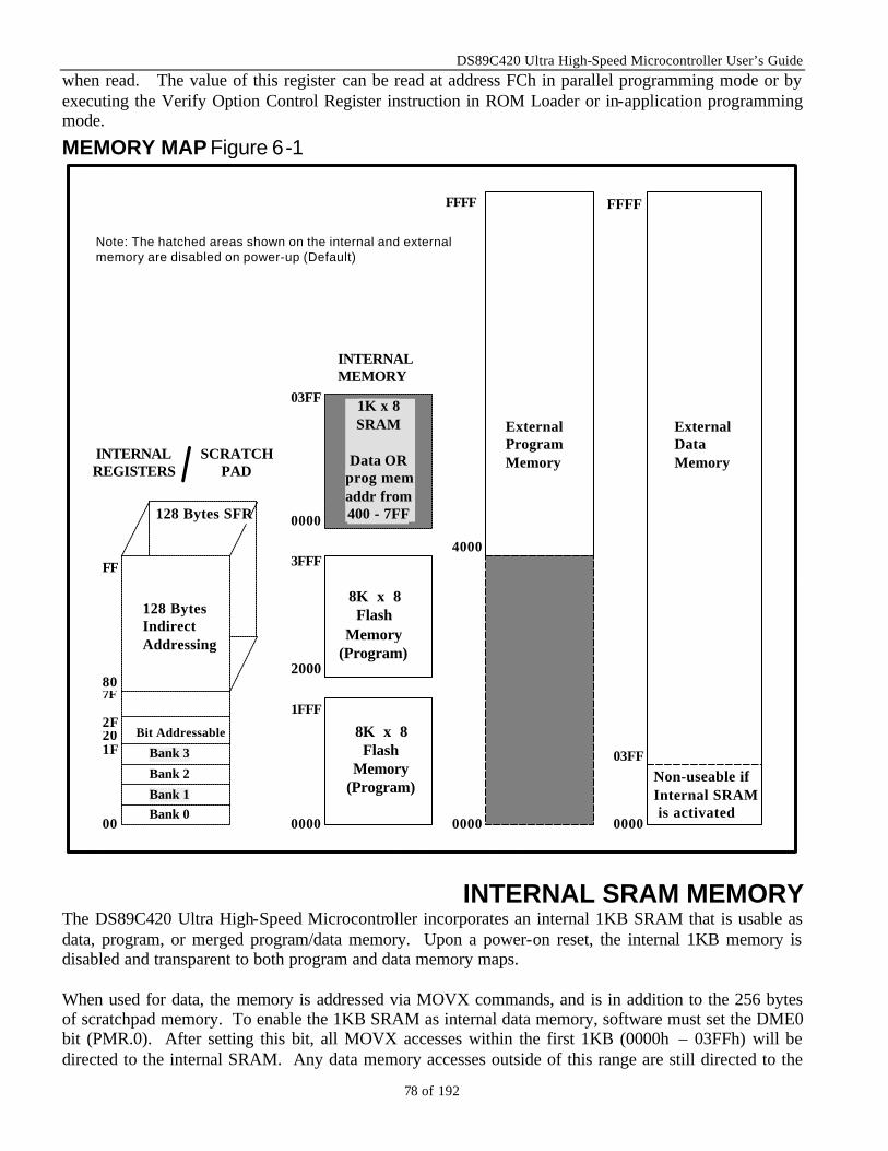
DS89C420 Ultra High-Speed Microcontroller User’s Guide
78 of 192
when read. The value of this register can be read at address FCh in parallel programming mode or by executing the Verify Option Control Register instruction in ROM Loader or in-application programming mode.
MEMORY MAP Figure 6-1
ExternalDataMemory
8K x 8Flash
Memory(Program)
1K x 8SRAM
Data ORprog mem addr from 400 - 7FF
128 BytesIndirect Addressing
Bit Addressable
Bank 3
Bank 2
Bank 1Bank 0
00
1F202F
7F80
128 Bytes SFR
FF
0000
1FFF
2000
3FFF
INTERNALMEMORY
03FF
0000
FFFF FFFF
4000
00000000
03FF
ExternalProgramMemoryINTERNAL
REGISTERS
8K x 8Flash
Memory(Program)
SCRATCHPAD
Note: The hatched areas shown on the internal and external memory are disabled on power-up (Default)
Non-useable if Internal SRAM is activated
INTERNAL SRAM MEMORY The DS89C420 Ultra High-Speed Microcontroller incorporates an internal 1KB SRAM that is usable as data, program, or merged program/data memory. Upon a power-on reset, the internal 1KB memory is disabled and transparent to both program and data memory maps. When used for data, the memory is addressed via MOVX commands, and is in addition to the 256 bytes of scratchpad memory. To enable the 1KB SRAM as internal data memory, software must set the DME0 bit (PMR.0). After setting this bit, all MOVX accesses within the first 1KB (0000h – 03FFh) will be directed to the internal SRAM. Any data memory accesses outside of this range are still directed to the
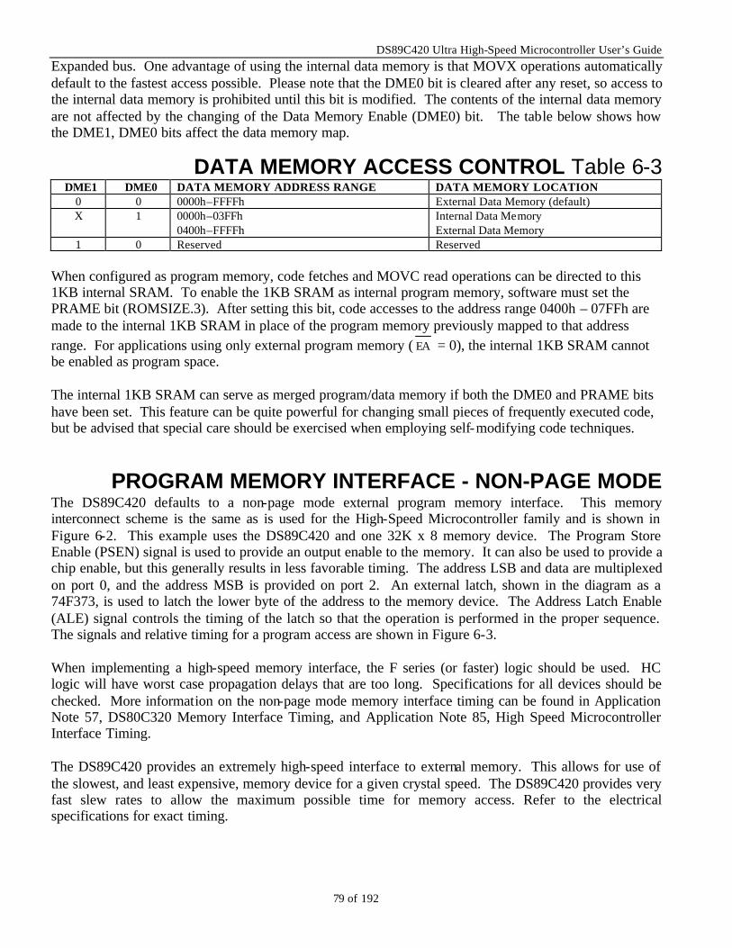
DS89C420 Ultra High-Speed Microcontroller User’s Guide
79 of 192
Expanded bus. One advantage of using the internal data memory is that MOVX operations automatically default to the fastest access possible. Please note that the DME0 bit is cleared after any reset, so access to the internal data memory is prohibited until this bit is modified. The contents of the internal data memory are not affected by the changing of the Data Memory Enable (DME0) bit. The table below shows how the DME1, DME0 bits affect the data memory map.
DATA MEMORY ACCESS CONTROL Table 6-3 DME1 DME0 DATA MEMORY ADDRESS RANGE DATA MEMORY LOCATION
0 0 0000h–FFFFh External Data Memory (default) X 1 0000h–03FFh
0400h–FFFFh Internal Data Memory External Data Memory
1 0 Reserved Reserved When configured as program memory, code fetches and MOVC read operations can be directed to this 1KB internal SRAM. To enable the 1KB SRAM as internal program memory, software must set the PRAME bit (ROMSIZE.3). After setting this bit, code accesses to the address range 0400h – 07FFh are made to the internal 1KB SRAM in place of the program memory previously mapped to that address range. For applications using only external program memory ( EA = 0), the internal 1KB SRAM cannot be enabled as program space. The internal 1KB SRAM can serve as merged program/data memory if both the DME0 and PRAME bits have been set. This feature can be quite powerful for changing small pieces of frequently executed code, but be advised that special care should be exercised when employing self-modifying code techniques.
PROGRAM MEMORY INTERFACE - NON-PAGE MODE The DS89C420 defaults to a non-page mode external program memory interface. This memory interconnect scheme is the same as is used for the High-Speed Microcontroller family and is shown in Figure 6-2. This example uses the DS89C420 and one 32K x 8 memory device. The Program Store Enable (PSEN) signal is used to provide an output enable to the memory. It can also be used to provide a chip enable, but this generally results in less favorable timing. The address LSB and data are multiplexed on port 0, and the address MSB is provided on port 2. An external latch, shown in the diagram as a 74F373, is used to latch the lower byte of the address to the memory device. The Address Latch Enable (ALE) signal controls the timing of the latch so that the operation is performed in the proper sequence. The signals and relative timing for a program access are shown in Figure 6-3. When implementing a high-speed memory interface, the F series (or faster) logic should be used. HC logic will have worst case propagation delays that are too long. Specifications for all devices should be checked. More information on the non-page mode memory interface timing can be found in Application Note 57, DS80C320 Memory Interface Timing, and Application Note 85, High Speed Microcontroller Interface Timing. The DS89C420 provides an extremely high-speed interface to external memory. This allows for use of the slowest, and least expensive, memory device for a given crystal speed. The DS89C420 provides very fast slew rates to allow the maximum possible time for memory access. Refer to the electrical specifications for exact timing.

DS89C420 Ultra High-Speed Microcontroller User’s Guide
80 of 192
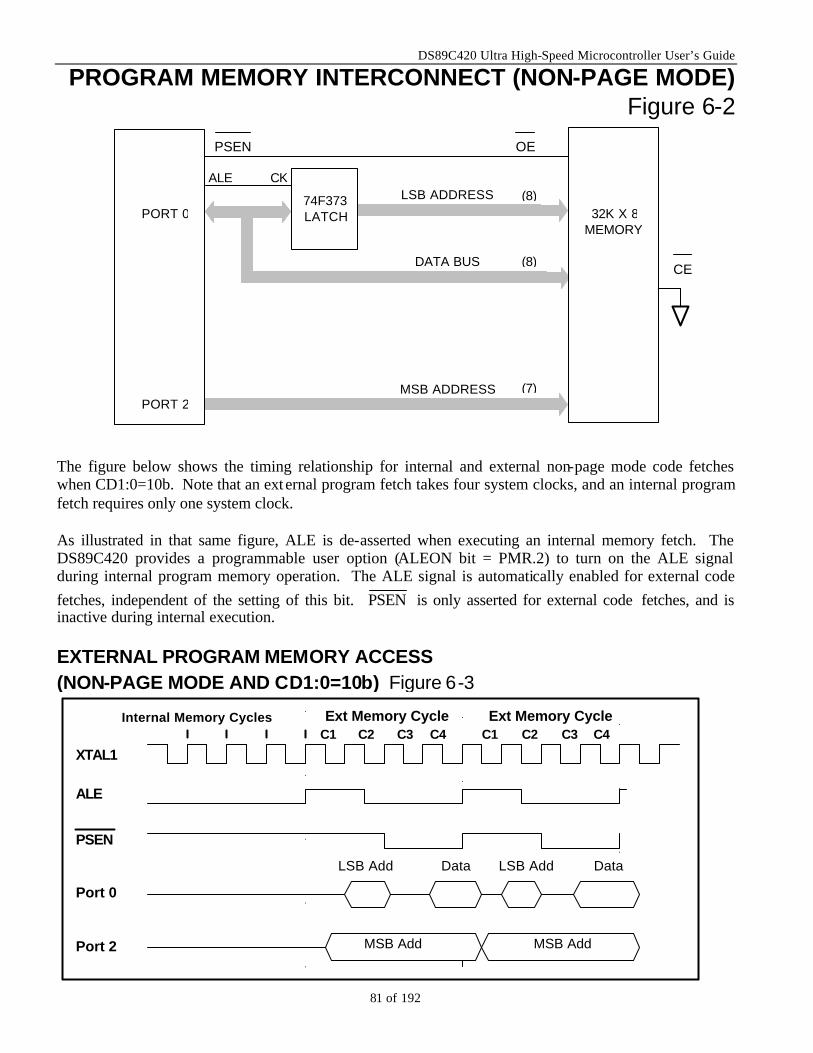
DS89C420 Ultra High-Speed Microcontroller User’s Guide
81 of 192
PROGRAM MEMORY INTERCONNECT (NON-PAGE MODE) Figure 6-2
The figure below shows the timing relationship for internal and external non-page mode code fetches when CD1:0=10b. Note that an external program fetch takes four system clocks, and an internal program fetch requires only one system clock. As illustrated in that same figure, ALE is de-asserted when executing an internal memory fetch. The DS89C420 provides a programmable user option (ALEON bit = PMR.2) to turn on the ALE signal during internal program memory operation. The ALE signal is automatically enabled for external code fetches, independent of the setting of this bit. PSEN is only asserted for external code fetches, and is inactive during internal execution.
EXTERNAL PROGRAM MEMORY ACCESS (NON-PAGE MODE AND CD1:0=10b) Figure 6-3
Internal Memory CyclesC2 C3 C4 C1 C2 C3 C4
XTAL1
ALE
Port 0
Port 2
PSEN
C1Ext Memory CycleExt Memory Cycle
MSB Add MSB Add
LSB Add Data LSB Add Data
DS80C320
PSEN
ALE CK
74F373 LATCH
LSB ADDRESS
DATA BUS
MSB ADDRESS PORT 2
(8)
(7)
32K X 8 MEMORY
(8)
OE
CE
PORT 0
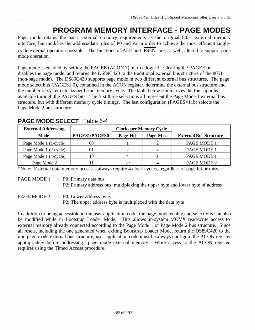
DS89C420 Ultra High-Speed Microcontroller User’s Guide
82 of 192
PROGRAM MEMORY INTERFACE - PAGE MODES Page mode retains the basic external circuitry requirements as the original 8051 external memory interface, but modifies the address/data roles of P0 and P2 in order to achieve the most efficient single-cycle external operation possible. The functions of ALE and PSEN are, as well, altered to support page mode operation. Page mode is enabled by setting the PAGEE (ACON.7) bit to a logic 1. Clearing the PAGEE bit disables the page mode, and returns the DS89C420 to the traditional external bus structure of the 8051 (non-page mode). The DS89C420 supports page mode in two different external bus structures. The page mode select bits (PAGES1:0), contained in the ACON register, determine the external bus structure and the number of system clocks per basic memory cycle. The table below summarizes the four options available through the PAGES bits. The first three selections all represent the Page Mode 1 external bus structure, but with different memory cycle timings. The last configuration (PAGES=11b) selects the Page Mode 2 bus structure.
PAGE MODE SELECT Table 6-4 External Addressing Clocks per Memory Cycle
Mode PAGES1:PAGES0 Page-Hit Page-Miss External Bus Structure
Page Mode 1 (1-cycle) 00 1 2 PAGE MODE 1 Page Mode 1 (2-cycle) 01 2 4 PAGE MODE 1 Page Mode 1 (4-cycle) 10 4 8 PAGE MODE 1
Page Mode 2 11 2* 4 PAGE MODE 2 *Note: External data memory accesses always require 4 clock cycles, regardless of page hit or miss. PAGE MODE 1 P0: Primary data bus. P2: Primary address bus, multiplexing the upper byte and lower byte of address PAGE MODE 2: P0: Lower address byte. P2: The upper address byte is multiplexed with the data byte In addition to being accessible to the user application code, the page mode enable and select bits can also be modified while in Bootstrap Loader Mode. This allows in-system MOVX read/write access to external memory already connected according to the Page Mode 1 or Page Mode 2 bus structure. Since all resets, including the one generated when exiting Bootstrap Loader Mode, return the DS89C420 to the non-page mode external bus structure, user application code must be always configure the ACON register appropriately before addressing page mode external memory. Write access to the ACON register requires using the Timed Access procedure.
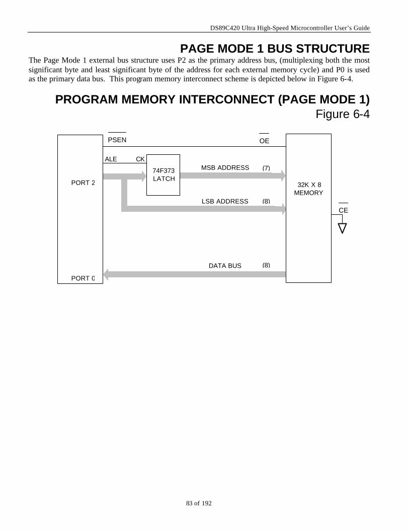
DS89C420 Ultra High-Speed Microcontroller User’s Guide
83 of 192
PAGE MODE 1 BUS STRUCTURE The Page Mode 1 external bus structure uses P2 as the primary address bus, (multiplexing both the most significant byte and least significant byte of the address for each external memory cycle) and P0 is used as the primary data bus. This program memory interconnect scheme is depicted below in Figure 6-4.
PROGRAM MEMORY INTERCONNECT (PAGE MODE 1) Figure 6-4
PSEN
DS80C320
ALE CK
74F373 LATCH
MSB ADDRESS
LSB ADDRESS
DATA BUS
PORT 0
(8)
(8)
32K X 8
MEMORY
(7)
OE
CE
PORT 2
DS89C420 Ultra High-Speed Microcontroller User’s Guide
84 of 192
During external code fetches, P0 will be held in a high- impedance state by the processor. Opcodes are driven by the external memory onto P0 and latched on the rising edge of PSEN at the end of the external fetch cycle.
§ A page miss occurs when the most significant byte of the subsequent address is different from the last address. The external memory machine cycle can be 2, 4 or 8 system clocks in length for a page miss.
§ A page hit occurs when the most significant byte of the subsequent address does not change from the last address. The external memory machine cycle can be 1, 2 or 4 system clocks in length for a page hit.
During a page hit, P2 drives Addr [7:0] of the 16-bit address while the most significant address byte is held in the external address latches. PSEN , RD , and WR will strobe accordingly for the appropriate operation on the P0 data bus. There is no ALE assertion for page hits. During a page miss, P2 drives the Addr [15:8] of the 16-bit address and holds it for the duration of the first half of the memory cycle to allow the external address latches to latch the new most significant address byte. ALE is asserted to strobe the external address latches. During this operation, PSEN , RD , and WR are all held in inactive states and P0 is in a high- impedance state. The following half memory cycle is executed as a page hit cycle and the appropriate operation takes place. A page miss may occur at set intervals or during external operations that require a memory access into a page of memory that has not been accessed during the last external cycle. Generally, the first external memory access causes a page miss. The new page address is stored internally, and is used to detect a page miss for the current external memory cycle. Note that there are a few exceptions for this mode of operation when PAGES1 and PAGES2 are set to 00b:
§ PSEN is asserted for both page hit and page miss for a full clock cycle § The execution of external MOVX instruction causes a page miss, and § A page miss occurs when fetching the next external instruction following the execution of an external
MOVX instruction. The figure below shows external memory cycles for the Page Mode 1 bus structure. The first case illustrates a back to back MOVX execution sequence for one cycle page mode (PAGES1:0=00b). PSEN remains active during page hit cycles, and page misses are forced during and after MOVX executions, independent of the most significant byte of the subsequent addresses. The second case illustrates a MOVX execution sequence for two cycle page mode (PAGES1:0=01b). PSEN is active for a full clock cycle in code fetches. Note that the page misses in this sequence are caused by changing of the most significant byte of the data address. The third case illustrates a MOVX execution sequence for four cycle page mode (PAGES1:0=10b). There is no page miss in this execution cyc le as the most significant byte of the data address is assumed to match the last program address.

DS89C420 Ultra High-Speed Microcontroller User’s Guide
85 of 192
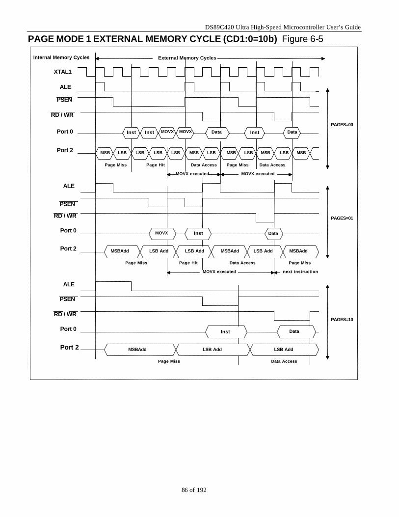
DS89C420 Ultra High-Speed Microcontroller User’s Guide
86 of 192
PAGE MODE 1 EXTERNAL MEMORY CYCLE (CD1:0=10b) Figure 6-5
Internal Memory Cycles
XTAL1
ALE
Port 0
Port 2
DataData Inst
MSB MSB MSB MSB MSB LSB LSB LSB LSB LSB LSB
Inst Inst
External Memory Cycles
Page MissPage HitPage Miss Data Access Data Access
PAGES=00
ALE
PSEN
MOVX Inst Data
Page Miss Page MissData AccessPage Hit
MSBAdd LSB Add LSB Add MSBAdd MSBAddLSB Add
PAGES=01
Port 0
Port 2
MSBAdd LSB Add LSB Add
Inst Data
Port 2
Port 0
PSEN
ALE
Page Miss Data Access
RD / WR
RD / WRPAGES=10
RD / WR
MOVX MOVX
LSB
PSEN
MOVX executed
MOVX executedMOVX executed
next instruction
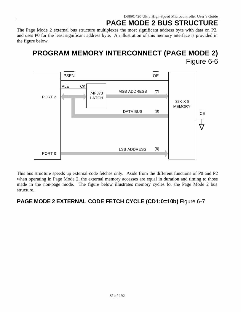
DS89C420 Ultra High-Speed Microcontroller User’s Guide
87 of 192
PAGE MODE 2 BUS STRUCTURE The Page Mode 2 external bus structure multiplexes the most significant address byte with data on P2, and uses P0 for the least significant address byte. An illustration of this memory interface is provided in the figure below.
PROGRAM MEMORY INTERCONNECT (PAGE MODE 2) Figure 6-6
This bus structure speeds up external code fetches only. Aside from the different functions of P0 and P2 when operating in Page Mode 2, the external memory accesses are equal in duration and timing to those made in the non-page mode. The figure below illustrates memory cycles for the Page Mode 2 bus structure.
PAGE MODE 2 EXTERNAL CODE FETCH CYCLE (CD1:0=10b) Figure 6-7
DS80C320
PSEN
ALE CK
74F373 LATCH
MSB ADDRESS
DATA BUS
LSB ADDRESS PORT 0
(8)
(8)
32K X 8
MEMORY
(7)
OE
CE
PORT 2
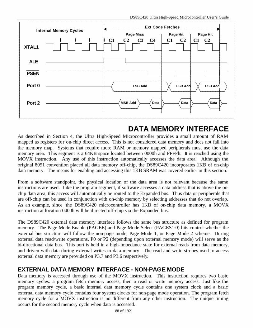
DS89C420 Ultra High-Speed Microcontroller User’s Guide
88 of 192
Internal Memory Cycles
C2 C3 C4 C1 C2 C1 C2XTAL1
ALE
Port 0
Port 2
PSEN
C1
Ext Code Fetches
Page Miss Page Hit Page Hit
Data Data
LSB AddLSB Add LSB Add
DataMSB Add
DATA MEMORY INTERFACE
As described in Section 4, the Ultra High-Speed Microcontroller provides a small amount of RAM mapped as registers for on-chip direct access. This is not considered data memory and does not fall into the memory map. Systems that require more RAM or memory mapped peripherals must use the data memory area. This segment is a 64KB space located between 0000h and FFFFh. It is reached using the MOVX instruction. Any use of this instruction automatically accesses the data area. Although the original 8051 convention placed all data memory off-chip, the DS89C420 incorporates 1KB of on-chip data memory. The means for enabling and accessing this 1KB SRAM was covered earlier in this section. From a software standpoint, the physical location of the data area is not relevant because the same instructions are used. Like the program segment, if software accesses a data address that is above the on-chip data area, this access will automatically be routed to the Expanded bus. Thus data or peripherals that are off-chip can be used in conjunction with on-chip memory by selecting addresses that do not overlap. As an example, since the DS89C420 microcontroller has 1KB of on-chip data memory, a MOVX instruction at location 0400h will be directed off-chip via the Expanded bus. The DS89C420 external data memory interface follows the same bus structure as defined for program memory. The Page Mode Enable (PAGEE) and Page Mode Select (PAGES1:0) bits control whether the external bus structure will follow the non-page mode, Page Mode 1, or Page Mode 2 scheme. During external data read/write operations, P0 or P2 (depending upon external memory mode) will serve as the bi-directional data bus. This port is held in a high- impedance state for external reads from data memory, and driven with data during external writes to data memory. The read and write strobes used to access external data memory are provided on P3.7 and P3.6 respectively.
EXTERNAL DATA MEMORY INTERFACE - NON-PAGE MODE Data memory is accessed through use of the MOVX instruction. This instruction requires two basic memory cycles: a program fetch memory access, then a read or write memory access. Just like the program memory cycle, a basic internal data memory cycle contains one system clock and a basic external data memory cycle contains four system clocks for non-page mode operation. The program fetch memory cycle for a MOVX instruction is no different from any other instruction. The unique timing occurs for the second memory cycle when data is accessed.
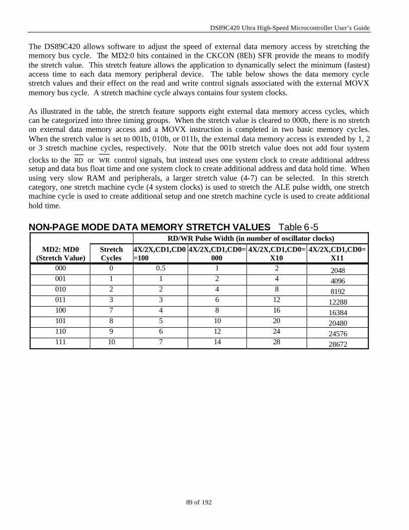
DS89C420 Ultra High-Speed Microcontroller User’s Guide
89 of 192
The DS89C420 allows software to adjust the speed of external data memory access by stretching the memory bus cycle. The MD2:0 bits contained in the CKCON (8Eh) SFR provide the means to modify the stretch value. This stretch feature allows the application to dynamically select the minimum (fastest) access time to each data memory peripheral device. The table below shows the data memory cycle stretch values and their effect on the read and write control signals associated with the external MOVX memory bus cycle. A stretch machine cycle always contains four system clocks. As illustrated in the table, the stretch feature supports eight external data memory access cycles, which can be categorized into three timing groups. When the stretch value is cleared to 000b, there is no stretch on external data memory access and a MOVX instruction is completed in two basic memory cyc les. When the stretch value is set to 001b, 010b, or 011b, the external data memory access is extended by 1, 2 or 3 stretch machine cycles, respectively. Note that the 001b stretch value does not add four system clocks to the RD or WR control signals, but instead uses one system clock to create additional address setup and data bus float time and one system clock to create additional address and data hold time. When using very slow RAM and peripherals, a larger stretch value (4-7) can be selected. In this stretch category, one stretch machine cycle (4 system clocks) is used to stretch the ALE pulse width, one stretch machine cycle is used to create additional setup and one stretch machine cycle is used to create additional hold time.
NON-PAGE MODE DATA MEMORY STRETCH VALUES Table 6-5 RD/WR Pulse Width (in number of oscillator clocks)
MD2: MD0 (Stretch Value)
Stretch Cycles
4X/2X,CD1,CD0=100
4X/2X,CD1,CD0=000
4X/2X,CD1,CD0=X10
4X/2X,CD1,CD0=X11
000 0 0.5 1 2 2048 001 1 1 2 4 4096 010 2 2 4 8 8192 011 3 3 6 12 12288 100 7 4 8 16 16384 101 8 5 10 20 20480 110 9 6 12 24 24576 111 10 7 14 28 28672
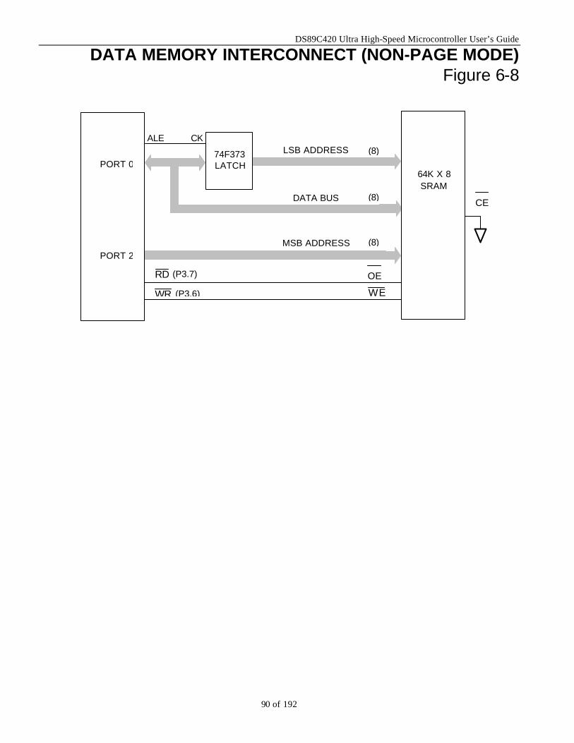
DS89C420 Ultra High-Speed Microcontroller User’s Guide
90 of 192
DATA MEMORY INTERCONNECT (NON-PAGE MODE) Figure 6-8
RD (P3.7)
WR (P3.6) WE
DS80C320
ALE CK
74F373 LATCH
LSB ADDRESS
DATA BUS
MSB ADDRESS PORT 2
(8)
(8)
64K X 8 SRAM
(8)
OE
CE
PORT 0
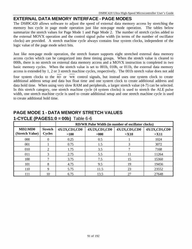
DS89C420 Ultra High-Speed Microcontroller User’s Guide
91 of 192
EXTERNAL DATA MEMORY INTERFACE - PAGE MODES The DS89C420 allows software to adjust the speed of external data memory access by stretching the memory bus cycle in page mode operation just like non-page mode operation. The tables below summarize the stretch values for Page Mode 1 and Page Mode 2. The number of stretch cycles added to the external MOVX operation and the control signal pulse width (in terms of the number of oscillator clocks) are provided. A stretch machine cycle always contains four system clocks, independent of the logic value of the page mode select bits. Just like non-page mode operation, the stretch feature supports eight stretched external data memory access cycles which can be categorized into three timing groups. When the stretch value is cleared to 000b, there is no stretch on external data memory access and a MOVX instruction is completed in two basic memory cycles. When the stretch value is set to 001b, 010b, or 011b, the external data memory access is extended by 1, 2 or 3 stretch machine cycles, respectively. The 001b stretch value does not add four system clocks to the RD or WR control signals, but instead uses one system clock to create additional address setup and data bus float time and one system clock to create additional address and data hold time. When using very slow RAM and peripherals, a larger stretch value (4-7) can be selected. In this stretch category, one stretch machine cycle (4 system clocks) is used to stretch the ALE pulse width, one stretch machine cycle is used to create additional setup and one stretch machine cycle is used to create additional hold time.
PAGE MODE 1 - DATA MEMORY STRETCH VALUES 1-CYCLE (PAGES1:0 = 00b) Table 6-6
RD/WR Pulse Width (in number of oscillator clocks) MD2:MD0
(Stretch Value) Stretch Cycles
4X/2X,CD1,CD0 =100
4X/2X,CD1,CD0 =000
4X/2X,CD1,CD0 =X10
4X/2X,CD1,CD0 =X11
000 0 0.25 0.5 1 1024 001 1 0.75 1.5 3 3072 010 2 1.75 3.5 7 7168 011 3 2.75 5.5 11 11264 100 7 3.75 7.5 15 15360 101 8 4.75 9.5 19 19456 110 9 5.75 11.5 23 23552 111 10 6.75 13.5 27 27648
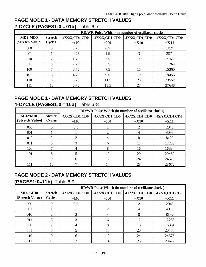
DS89C420 Ultra High-Speed Microcontroller User’s Guide
92 of 192
PAGE MODE 1 - DATA MEMORY STRETCH VALUES 2-CYCLE (PAGES1:0 = 01b) Table 6-7
RD/WR Pulse Width (in number of oscillator clocks) MD2:MD0
(Stretch Value) Stretch Cycles
4X/2X,CD1,CD0 =100
4X/2X,CD1,CD0 =000
4X/2X,CD1,CD0 =X10
4X/2X,CD1,CD0 =X11
000 0 0.25 0.5 1 1024 001 1 0.75 1.5 3 3072 010 2 1.75 3.5 7 7168 011 3 2.75 5.5 11 11264 100 7 3.75 7.5 15 15360 101 8 4.75 9.5 19 19456 110 9 5.75 11.5 23 23552 111 10 6.75 13.5 27 27648
PAGE MODE 1 - DATA MEMORY STRETCH VALUES 4-CYCLE (PAGES1:0 = 10b) Table 6-8
RD/WR Pulse Width (in number of oscillator clocks) MD2:MD0
(Stretch Value) Stretch Cycles
4X/2X,CD1,CD0 =100
4X/2X,CD1,CD0 =000
4X/2X,CD1,CD0 =X10
4X/2X,CD1,CD0 =X11
000 0 0.5 1 2 2048 001 1 1 2 4 4096 010 2 2 4 8 8192 011 3 3 6 12 12288 100 7 4 8 16 16384 101 8 5 10 20 20480 110 9 6 12 24 24576 111 10 7 14 28 28672
PAGE MODE 2 - DATA MEMORY STRETCH VALUES (PAGES1:0=11b) Table 6-9
RD/WR Pulse Width (in number of oscillator clocks) MD2:MD0
(Stretch Value) Stretch Cycles
4X/2X,CD1,CD0 =100
4X/2X,CD1,CD0 =000
4X/2X,CD1,CD0 =X10
4X/2X,CD1,CD0 =X11
000 0 0.5 1 2 2048 001 1 1 2 4 4096 010 2 2 4 8 8192 011 3 3 6 12 12288 100 7 4 8 16 16384 101 8 5 10 20 20480 110 9 6 12 24 24576 111 10 7 14 28 28672
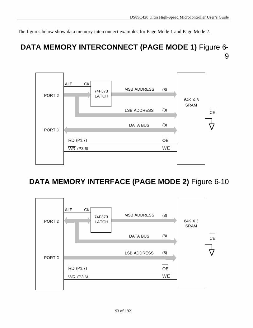
DS89C420 Ultra High-Speed Microcontroller User’s Guide
93 of 192
The figures below show data memory interconnect examples for Page Mode 1 and Page Mode 2.
DATA MEMORY INTERCONNECT (PAGE MODE 1) Figure 6-
9
DATA MEMORY INTERFACE (PAGE MODE 2) Figure 6-10
DS80C320
ALE CK
74F373 LATCH
MSB ADDRESS
LSB ADDRESS
DATA BUS PORT 0
(8)
(8)
64K X 8 SRAM
(8)
CE
PORT 2
OE
RD (P3.7)
WR (P3.6) WE
DS80C320
ALE CK
74F373 LATCH
MSB ADDRESS
DATA BUS
LSB ADDRESS PORT 0
(8)
(8)
64K X 8 SRAM
(8)
OE
CE
PORT 2
RD (P3.7)
WR (P3.6) WE
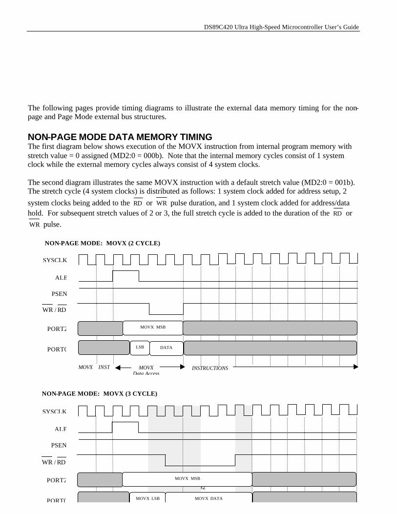
DS89C420 Ultra High-Speed Microcontroller User’s Guide
94 of 192
The following pages provide timing diagrams to illustrate the external data memory timing for the non-page and Page Mode external bus structures. NON-PAGE MODE DATA MEMORY TIMING The first diagram below shows execution of the MOVX instruction from internal program memory with stretch value = 0 assigned (MD2:0 = 000b). Note that the internal memory cycles consist of 1 system clock while the external memory cycles always consist of 4 system clocks. The second diagram illustrates the same MOVX instruction with a default stretch value (MD2:0 = 001b). The stretch cycle (4 system clocks) is distributed as follows: 1 system clock added for address setup, 2 system clocks being added to the RD or WR pulse duration, and 1 system clock added for address/data hold. For subsequent stretch values of 2 or 3, the full stretch cycle is added to the duration of the RD or WR pulse.
SYSCLK
ALE
PSEN
PORT2
PORT0
MOVX MSB
MOVX
MOVX Data Access
INSTRUCTIONS
DATA LSB
INST
WR / RD
NON-PAGE MODE: MOVX (2 CYCLE)
SYSCLK
ALE
PSEN
PORT2
PORT0
MOVX LSB
MOVX DATA
MOVX MSB
WR / RD
NON-PAGE MODE: MOVX (3 CYCLE)
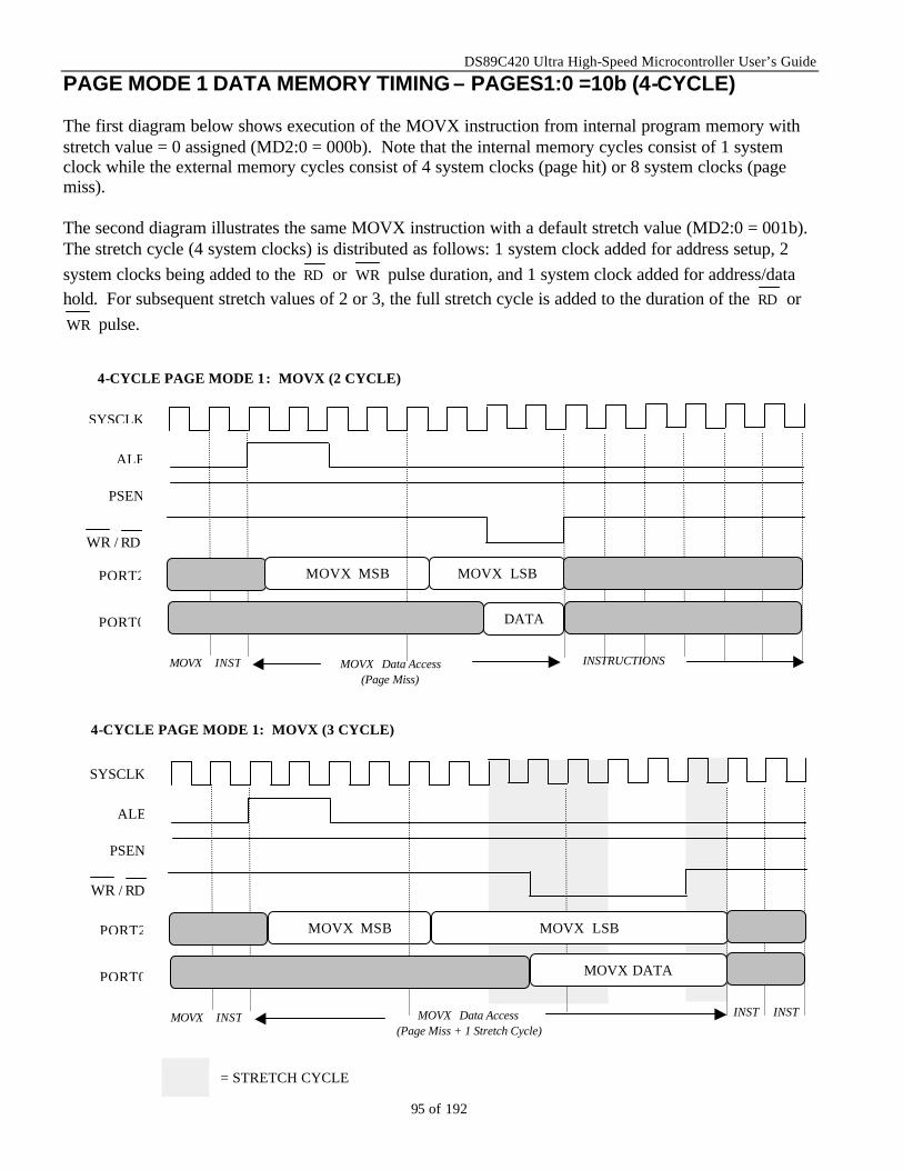
DS89C420 Ultra High-Speed Microcontroller User’s Guide
95 of 192
PAGE MODE 1 DATA MEMORY TIMING – PAGES1:0 =10b (4-CYCLE) The first diagram below shows execution of the MOVX instruction from internal program memory with stretch value = 0 assigned (MD2:0 = 000b). Note that the internal memory cycles consist of 1 system clock while the external memory cycles consist of 4 system clocks (page hit) or 8 system clocks (page miss). The second diagram illustrates the same MOVX instruction with a default stretch value (MD2:0 = 001b). The stretch cycle (4 system clocks) is distributed as follows: 1 system clock added for address setup, 2 system clocks being added to the RD or WR pulse duration, and 1 system clock added for address/data hold. For subsequent stretch values of 2 or 3, the full stretch cycle is added to the duration of the RD or WR pulse.
SYSCLK
ALE
PSEN
PORT2
PORT0
MOVX MSB
MOVX
MOVX Data Access (Page Miss)
INSTRUCTIONS
DATA
MOVX LSB
INST
WR / RD
4-CYCLE PAGE MODE 1: MOVX (2 CYCLE)
WR / RD
SYSCLK
ALE
PSEN
PORT2
PORT0
MOVX MSB
MOVX
MOVX Data Access (Page Miss + 1 Stretch Cycle)
INST
MOVX DATA
MOVX LSB
INST
= STRETCH CYCLE
INST
4-CYCLE PAGE MODE 1: MOVX (3 CYCLE)
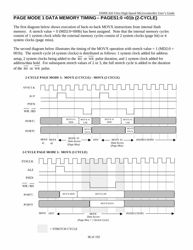
DS89C420 Ultra High-Speed Microcontroller User’s Guide
96 of 192
PAGE MODE 1 DATA MEMORY TIMING – PAGES1:0 =01b (2-CYCLE) The first diagram below shows execution of back-to-back MOVX instructions from internal flash memory. A stretch value = 0 (MD2:0=000b) has been assigned. Note that the internal memory cycles consist of 1 system clock while the external memory cycles consist of 2 system clocks (page hit) or 4 system clocks (page miss). The second diagram below illustrates the timing of the MOVX operation with stretch value = 1 (MD2:0 = 001b). The stretch cycle (4 system clocks) is distributed as follows: 1 system clock added for address setup, 2 system clocks being added to the RD or WR pulse duration, and 1 system clock added for address/data hold. For subsequent stretch values of 2 or 3, the full stretch cycle is added to the duration of the RD or WR pulse.
MOVX #2 LSB
MOVX #1 LSB
MOVX #1 MSB
SYSCLK
ALE
PSEN
PORT2
PORT0
MOVX #1
MOVX #2
MOVX #1 Data Access (Page Miss)
MOVX #2 Data Access (Page Miss)
INST
INSTRUCTIONS
MOVX DATA
MOVX #2 MSB
MOVX DATA
WR / RD
2-CYCLE PAGE MODE 1: MOVX (2 CYCLE) – MOVX (2 CYCLE)
SYSCLK
ALE
PSEN
PORT2
PORT0
MOVX MSB
MOVX
MOVX Data Access
(Page Miss + 1 Stretch Cycle)
INST
INSTRUCTIONS
MOVX DATA
MOVX LSB
= STRETCH CYCLE
WR / RD
2-CYCLE PAGE MODE 1: MOVX (3 CYCLE)
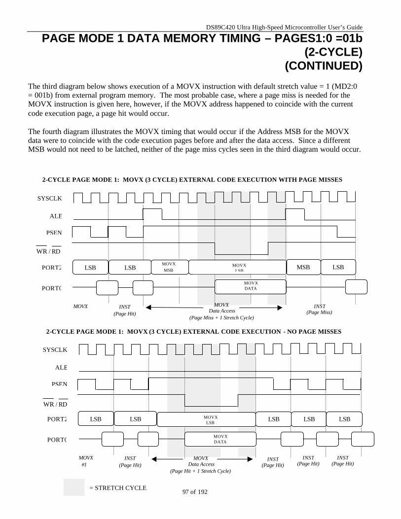
DS89C420 Ultra High-Speed Microcontroller User’s Guide
97 of 192
PAGE MODE 1 DATA MEMORY TIMING – PAGES1:0 =01b (2-CYCLE)
(CONTINUED) The third diagram below shows execution of a MOVX instruction with default stretch value = 1 (MD2:0 = 001b) from external program memory. The most probable case, where a page miss is needed for the MOVX instruction is given here, however, if the MOVX address happened to coincide with the current code execution page, a page hit would occur. The fourth diagram illustrates the MOVX timing that would occur if the Address MSB for the MOVX data were to coincide with the code execution pages before and after the data access. Since a different MSB would not need to be latched, neither of the page miss cycles seen in the third diagram would occur.
MOVX MSB
SYSCLK
ALE
PSEN
PORT2
PORT0
LSB
MOVX
MOVX Data Access
(Page Miss + 1 Stretch Cycle)
INST (Page Hit)
INST (Page Miss)
MOVX DATA
MSB LSB LSB
WR / RD
MOVX LSB
2-CYCLE PAGE MODE 1: MOVX (3 CYCLE) EXTERNAL CODE EXECUTION WITH PAGE MISSES
MOVX LSB
SYSCLK
ALE
PSEN
PORT2
PORT0
LSB
MOVX #1
MOVX Data Access
(Page Hit + 1 Stretch Cycle)
INST (Page Hit)
INST (Page Hit)
MOVX DATA
LSB LSB
LSB LSB
INST (Page Hit)
INST (Page Hit)
= STRETCH CYCLE
WR / RD
2-CYCLE PAGE MODE 1: MOVX (3 CYCLE) EXTERNAL CODE EXECUTION - NO PAGE MISSES
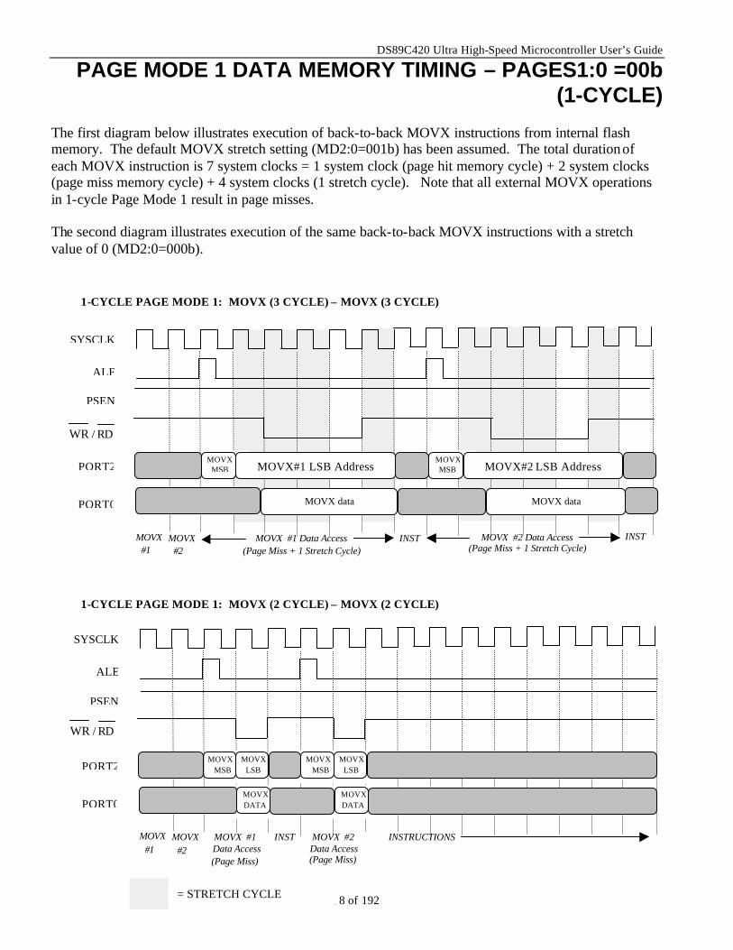
DS89C420 Ultra High-Speed Microcontroller User’s Guide
98 of 192
PAGE MODE 1 DATA MEMORY TIMING – PAGES1:0 =00b (1-CYCLE)
The first diagram below illustrates execution of back-to-back MOVX instructions from internal flash memory. The default MOVX stretch setting (MD2:0=001b) has been assumed. The total duration of each MOVX instruction is 7 system clocks = 1 system clock (page hit memory cycle) + 2 system clocks (page miss memory cycle) + 4 system clocks (1 stretch cycle). Note that all external MOVX operations in 1-cycle Page Mode 1 result in page misses. The second diagram illustrates execution of the same back-to-back MOVX instructions with a stretch value of 0 (MD2:0=000b).
WR / RD
MOVX MSB
MOVX MSB
SYSCLK
ALE
PSEN
PORT2
PORT0
MOVX data
MOVX #1
MOVX #2
MOVX#1 LSB Address
MOVX data
MOVX#2 LSB Address
MOVX #1 Data Access (Page Miss + 1 Stretch Cycle)
MOVX #2 Data Access (Page Miss + 1 Stretch Cycle)
INST
INST
1-CYCLE PAGE MODE 1: MOVX (3 CYCLE) – MOVX (3 CYCLE)
MOVX MOVX MSB LSB
SYSCLK
ALE
PSEN
PORT2
PORT0
MOVX #1
MOVX #2
MOVX #1 Data Access (Page Miss)
MOVX #2 Data Access (Page Miss)
INST
INSTRUCTIONS
MOVX DATA
MOVX MOVX MSB LSB
MOVX DATA
= STRETCH CYCLE
WR / RD
1-CYCLE PAGE MODE 1: MOVX (2 CYCLE) – MOVX (2 CYCLE)
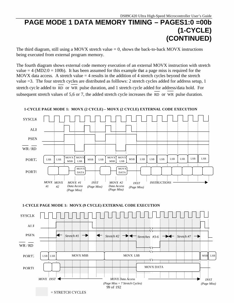
DS89C420 Ultra High-Speed Microcontroller User’s Guide
99 of 192
PAGE MODE 1 DATA MEMORY TIMING – PAGES1:0 =00b (1-CYCLE)
(CONTINUED) The third diagram, still using a MOVX stretch value = 0, shows the back-to-back MOVX instructions being executed from external program memory. The fourth diagram shows external code memory execution of an external MOVX instruction with stretch value = 4 (MD2:0 = 100b). It has been assumed for this example that a page miss is required for the MOVX data access. A stretch value = 4 results in the addition of 4 stretch cycles beyond the stretch value =3. The four stretch cycles are distributed as folllows: 2 stretch cycles added for address setup, 1 stretch cyc le added to RD or WR pulse duration, and 1 stretch cycle added for address/data hold. For subsequent stretch values of 5,6 or 7, the added stretch cycle increases the RD or WR pulse duration.
MSB LSB MOVX MOVX
MSB LSB
SYSCLK
ALE
PSEN
PORT2
PORT0
MOVX #1
MOVX #2
MOVX #1 Data Access (Page Miss)
MOVX #2 Data Access (Page Miss)
INST (Page Miss)
INSTRUCTIONS
MOVX DATA
MOVX MOVX MSB LSB
MOVX DATA
INST (Page Miss)
MSB LSB LSB LSB LSB LSB LSB LSB LSB LSB
WR / RD
1-CYCLE PAGE MODE 1: MOVX (2 CYCLE) – MOVX (2 CYCLE) EXTERNAL CODE EXECUTION
SYSCLK
ALE
PSEN
PORT2
PORT0
= STRETCH CYCLES
MOVX INST
MOVX MSB
MOVX LSB LSB LSB
MOVX Data Access (Page Miss + 7 Stretch Cycles)
MSB LSB
Stretch #1 Stretch #2 Stretch #7 Stretches #3-6
INST (Page Miss)
WR / RD
MOVX DATA
1-CYCLE PAGE MODE 1: MOVX (9 CYCLE) EXTERNAL CODE EXECUTION
DS89C420 Ultra High-Speed Microcontroller User’s Guide
100 of 192
PAGE MODE 2 DATA MEMORY TIMING – PAGES1:0 =11B (4-CYCLE) All external data memory accesses made using the Page Mode 2 external bus configuration require 4 system clocks. The MOVX timing will look identical to the non-page mode MOVX timing except that Port 2 will multiplex the MSB and data, while Port 0 will serve as the LSB.
DS89C420 Ultra High-Speed Microcontroller User’s Guide
101 of 192
DATA MEMORY ACCESS As mentioned earlier in this section, the Ultra High-Speed Microcontroller uses the MOVX instruction for data memory access. This includes off-chip RAM and memory mapped peripherals needing read/write access. Several aspects of the MOVX operation have been enhanced as compared to the original 8051. The principal improvements are in the areas of the MOVX timing and the Data Pointer. The MOVX instruction is used to generate read/write access to off-chip address locations. It has several addressing modes. The first uses the MOVX @ Ri command to reach a 256 byte block. This instruction uses the value in the designated working register to address one of 256 locations. The upper byte of the address is supplied by the value in the Port 2 latch. A second way to access data is the Data Pointer (DPTR). This 16-bit register provides an absolute address for data memory access. 16-bits cover the entire 64KB area. Thus the DPTR serves as a pointer to memory. Using the DPTR, the relevant instruction is MOVX @DPTR. The original 8051 contained one DPTR. While this provides access to the entire memory area, it is difficult to move data from one address to another. The Ultra High-Speed Microcontroller provides two Data Pointers. Thus software can load both a source and a destination address. The MOVX instruction will use the active pointer to direct the off-chip address. The Dual Data Pointers are called DPTR0 and DPTR1. DPTR0 is located at SFR addresses 82h and 83h. These are the locations used by the original 8051. No modification of standard code is needed to use DPTR0. The new DPTR is located at SFR 84h and 85h. The Data Pointer Select bit (SEL) chooses the active pointer and is located in bit position 0 of the DPS (86h) SFR. When DPS is set to 0, the DPTR0 is active. When set to 1, DPTR1 is used. All DPTR-related instructions use the currently selected DPTR for any activity. Each data pointer (DPTR0, DPTR1) has an associated control bit (ID0, ID1) that determines whether the INC DPTR operation results in an increment or decrement of the pointer. When the active data pointer ID (Increment/Decrement) control bit is clear, the INC DPTR instruction will increment the pointer, whereas a decrement will occur if the active pointer’s ID bit is set when the INC DPTR instruction is performed. ID0 = DPS.6 ID1 = DPS.7 Using the Dual Data Pointers for large block copy operations results in substantial code savings versus using a single data pointer since one data pointer can be used for the source address and the second pointer can be used as the destination address. The user switches between data pointers by toggling the SEL bit. One way of accomplishing this is by executing the INC DPS instruction. For these large block copy operations, the user must execute this instruction frequently to toggle between DPTR0 and DPTR1. To improve the speed and efficiency of moving data with Dual Data Pointers, the Ultra High-Speed Microcontroller contains a Toggle Select (TSL) bit. When this TSL bit (DPS.5) is set, execution of certain MOVX instructions automatically toggle the SEL bit in hardware, allowing removal of the INC DPS instruction and increasing execution speed. Copying large blocks of data also requires that the source and destination pointers index byte by byte through their respective data ranges. The traditional method for incrementing each pointer is through the use of the INC DPTR ins truction. The DS89C420 provides yet another means of accelerating data transfers with the implementation of an Auto Increment / Decrement bit (AID). When this AID bit (DPS.4) is set, execution of certain MOVX instructions automatically increments or decrements the active data pointer.
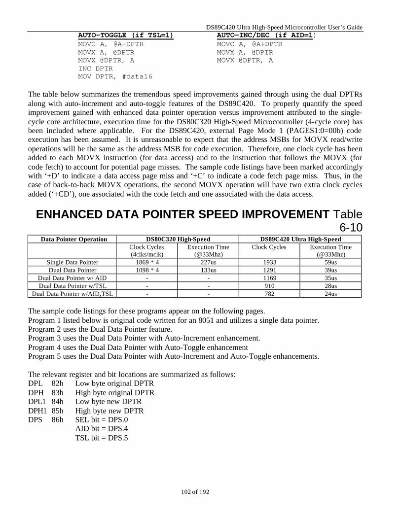
DS89C420 Ultra High-Speed Microcontroller User’s Guide
102 of 192
AUTO-TOGGLE (if TSL=1) AUTO-INC/DEC (if AID=1) MOVC A, @A+DPTR MOVC A, @A+DPTR MOVX A, @DPTR MOVX A, @DPTR MOVX @DPTR, A MOVX @DPTR, A INC DPTR MOV DPTR, #data16 The table below summarizes the tremendous speed improvements gained through using the dual DPTRs along with auto- increment and auto-toggle features of the DS89C420. To properly quantify the speed improvement gained with enhanced data pointer operation versus improvement attributed to the single-cycle core architecture, execution time for the DS80C320 High-Speed Microcontroller (4-cycle core) has been included where applicable. For the DS89C420, external Page Mode 1 (PAGES1:0=00b) code execution has been assumed. It is unreasonable to expect that the address MSBs for MOVX read/write operations will be the same as the address MSB for code execution. Therefore, one clock cycle has been added to each MOVX instruction (for data access) and to the instruction that follows the MOVX (for code fetch) to account for potential page misses. The sample code listings have been marked accordingly with ‘+D’ to indicate a data access page miss and ‘+C’ to indicate a code fetch page miss. Thus, in the case of back-to-back MOVX operations, the second MOVX operation will have two extra clock cycles added (‘+CD’), one associated with the code fetch and one associated with the data access.
ENHANCED DATA POINTER SPEED IMPROVEMENT Table 6-10
Data Pointer Operation DS80C320 High-Speed DS89C420 Ultra High-Speed Clock Cycles
(4clks/mclk) Execution Time
(@33Mhz) Clock Cycles Execution Time
(@33Mhz) Single Data Pointer 1869 * 4 227us 1933 59us Dual Data Pointer 1098 * 4 133us 1291 39us
Dual Data Pointer w/ AID - - 1169 35us Dual Data Pointer w/TSL - - 910 28us
Dual Data Pointer w/AID,TSL - - 782 24us The sample code listings for these programs appear on the following pages. Program 1 listed below is original code written for an 8051 and utilizes a single data pointer. Program 2 uses the Dual Data Pointer feature. Program 3 uses the Dual Data Pointer with Auto-Increment enhancement. Program 4 uses the Dual Data Pointer with Auto-Toggle enhancement Program 5 uses the Dual Data Pointer with Auto-Increment and Auto-Toggle enhancements. The relevant register and bit locations are summarized as follows: DPL 82h Low byte original DPTR DPH 83h High byte original DPTR DPL1 84h Low byte new DPTR DPH1 85h High byte new DPTR DPS 86h SEL bit = DPS.0
AID bit = DPS.4 TSL bit = DPS.5
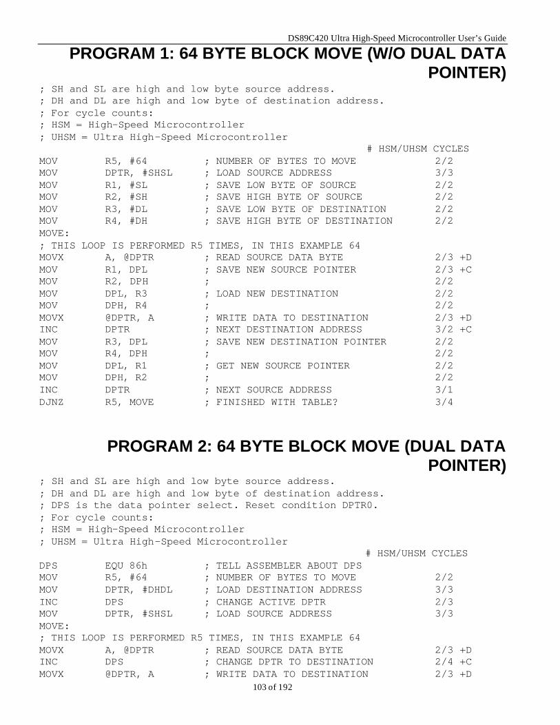
DS89C420 Ultra High-Speed Microcontroller User’s Guide
103 of 192
PROGRAM 1: 64 BYTE BLOCK MOVE (W/O DUAL DATA POINTER)
; SH and SL are high and low byte source address. ; DH and DL are high and low byte of destination address. ; For cycle counts: ; HSM = High-Speed Microcontroller ; UHSM = Ultra High-Speed Microcontroller # HSM/UHSM CYCLES MOV R5, #64 ; NUMBER OF BYTES TO MOVE 2/2 MOV DPTR, #SHSL ; LOAD SOURCE ADDRESS 3/3 MOV R1, #SL ; SAVE LOW BYTE OF SOURCE 2/2 MOV R2, #SH ; SAVE HIGH BYTE OF SOURCE 2/2 MOV R3, #DL ; SAVE LOW BYTE OF DESTINATION 2/2 MOV R4, #DH ; SAVE HIGH BYTE OF DESTINATION 2/2 MOVE: ; THIS LOOP IS PERFORMED R5 TIMES, IN THIS EXAMPLE 64 MOVX A, @DPTR ; READ SOURCE DATA BYTE 2/3 +D MOV R1, DPL ; SAVE NEW SOURCE POINTER 2/3 +C MOV R2, DPH ; 2/2 MOV DPL, R3 ; LOAD NEW DESTINATION 2/2 MOV DPH, R4 ; 2/2 MOVX @DPTR, A ; WRITE DATA TO DESTINATION 2/3 +D INC DPTR ; NEXT DESTINATION ADDRESS 3/2 +C MOV R3, DPL ; SAVE NEW DESTINATION POINTER 2/2 MOV R4, DPH ; 2/2 MOV DPL, R1 ; GET NEW SOURCE POINTER 2/2 MOV DPH, R2 ; 2/2 INC DPTR ; NEXT SOURCE ADDRESS 3/1 DJNZ R5, MOVE ; FINISHED WITH TABLE? 3/4
PROGRAM 2: 64 BYTE BLOCK MOVE (DUAL DATA POINTER)
; SH and SL are high and low byte source address. ; DH and DL are high and low byte of destination address. ; DPS is the data pointer select. Reset condition DPTR0. ; For cycle counts: ; HSM = High-Speed Microcontroller ; UHSM = Ultra High-Speed Microcontroller # HSM/UHSM CYCLES DPS EQU 86h ; TELL ASSEMBLER ABOUT DPS MOV R5, #64 ; NUMBER OF BYTES TO MOVE 2/2 MOV DPTR, #DHDL ; LOAD DESTINATION ADDRESS 3/3 INC DPS ; CHANGE ACTIVE DPTR 2/3 MOV DPTR, #SHSL ; LOAD SOURCE ADDRESS 3/3 MOVE: ; THIS LOOP IS PERFORMED R5 TIMES, IN THIS EXAMPLE 64 MOVX A, @DPTR ; READ SOURCE DATA BYTE 2/3 +D INC DPS ; CHANGE DPTR TO DESTINATION 2/4 +C MOVX @DPTR, A ; WRITE DATA TO DESTINATION 2/3 +D
DS89C420 Ultra High-Speed Microcontroller User’s Guide
104 of 192
INC DPTR ; NEXT DESTINATION ADDRESS 3/2 +C INC DPS ; CHANGE DATA POINTER TO SOURCE 2/3 INC DPTR ; NEXT SOURCE ADDRESS 3/1 DJNZ R5, MOVE ; FINISHED WITH TABLE? 3/4
PROGRAM 3: 64 BYTE BLOCK MOVE (DUAL DATA POINTER, AID)
; SH and SL are high and low byte source address. ; DH and DL are high and low byte of destination address. ; DPS is the data pointer select. Reset condition DPTR0. # UHSM CYCLES DPS EQU 86h ; TELL ASSEMBLER ABOUT DPS MOV R5, #64 ; NUMBER OF BYTES TO MOVE 2 ORL DPS, #10h ; SET AUTO-INC/DEC (AID) 3 MOV DPTR, #DHDL ; LOAD DESTINATION ADDRESS 3 INC DPS ; CHANGE ACTIVE DPTR 3 MOV DPTR, #SHSL ; LOAD SOURCE ADDRESS 3 MOVE: ; THIS LOOP IS PERFORMED R5 TIMES, IN THIS EXAMPLE 64 MOVX A, @DPTR ; READ SOURCE DATA BYTE 3 +D INC DPS ; CHANGE DPTR TO DESTINATION 4 +C MOVX @DPTR, A ; WRITE DATA TO DESTINATION 3 +D INC DPS ; CHANGE DATA POINTER TO SOURCE 4 +C DJNZ R5, MOVE ; FINISHED WITH TABLE? 4 ANL DPS, #0EFH ; CLEAR AUTO-INC/DEC 3
PROGRAM 4: 64 BYTE BLOCK MOVE (DUAL DATA POINTER, TSL)
; SH and SL are high and low byte source address. ; DH and DL are high and low byte of destination address. ; DPS is the data pointer select. Reset condition DPTR0. # UHSM CYCLES DPS EQU 86h ; TELL ASSEMBLER ABOUT DPS MOV R5, #64 ; NUMBER OF BYTES TO MOVE 2 ORL DPS, #20h ; SET TOGGLE SELECT (TSL) 3 MOV DPTR, #SHSL ; LOAD SOURCE ADDRESS 3 MOV DPTR, #DHDL ; LOAD DESTINATION ADDRESS 3 MOVE: ; THIS LOOP IS PERFORMED R5 TIMES, IN THIS EXAMPLE 64 MOVX A, @DPTR ; READ SOURCE DATA BYTE 3 +D MOVX @DPTR, A ; WRITE DATA TO DESTINATION 4 +CD INC DPTR ; NEXT SOURCE ADDRESS 2 +C INC DPTR ; NEXT DESTINATION ADDRESS 1 DJNZ R5, MOVE ; FINISHED WITH TABLE? 4 ANL DPS, #0DFh ; CLEAR TOGGLE SELECT 3
DS89C420 Ultra High-Speed Microcontroller User’s Guide
105 of 192
PROGRAM 5: 64 BYTE BLOCK MOVE (DUAL DATA POINTER, AID, TSL)
; SH and SL are high and low byte source address. ; DH and DL are high and low byte of destination address. ; DPS is the data pointer select. Reset condition DPTR0. # UHSM CYCLES DPS EQU 86h ; TELL ASSEMBLER ABOUT DPS MOV R5, #64 ; NUMBER OF BYTES TO MOVE 2 ORL DPS, #30h ; SET TOGGLE SELECT, AUTO-INC/DEC 3 MOV DPTR, #SHSL ; LOAD SOURCE ADDRESS 3 MOV DPTR, #DHDL ; LOAD DESTINATION ADDRESS 3 MOVE: ; THIS LOOP IS PERFORMED R5 TIMES, IN THIS EXAMPLE 64 MOVX A, @DPTR ; READ SOURCE DATA BYTE 3 +D MOVX @DPTR, A ; WRITE DATA TO DESTINATION 4 +CD DJNZ R5, MOVE ; FINISHED WITH TABLE? 5 +C ANL DPS, #0CFh ; CLEAR TSL, AID 3 Note that since each pass through the loop saves additional clock cycles when compared to the single DPTR approach, efficiency improvement when moving larger blocks is even greater using these features. Further speed improvement can be gained on the DS89C420 when executing from internal flash program memory since no code fetch page misses, ‘+C’, would occur. As an example, running program #5 from internal memory at 33 MHz would require only 19.8us (=1/33 MHz * (14 + 64 * 10)).

DS89C420 Ultra High-Speed Microcontroller User’s Guide
106 of 192
SECTION 7: POWER MANAGEMENT The DS89C420 has several features that relate to power consumption and management. They provide a combination of controlled operation in unreliable power applications and reduced power consumption in portable or battery powered applications. The range of features is shown below with details to follow. POWER MANAGEMENT EARLY WARNING POWER FAIL INTERRUPT POWER FAIL/POWER ON RESET BAND–GAP SELECT WATCHDOG WAKE UP FROM IDLE POWER SAVING IDLE MODE STOP MODE RING WAKE UP FROM STOP POWER MANAGEMENT MODE PRECISION VOLTAGE MONITOR The DS89C420 uses a precision band-gap reference and other analog circuits to monitor the state of the power supply during power-up and power-down transitions. This obviates the need for external circuits to perform these functions which other microcontroller systems would require. The band-gap reference provides a precise voltage to compare with VCC. When VCC begins to drop, the Power Monitor compares it to its reference. This enables the analog circuits to detect when VCC passes through predetermined thresholds, VPFW and VRST . These are specified in the DS89C420 product data sheet. EARLY WARNING POWER FAIL INTERRUPT The DS89C420 which incorporates a precision voltage reference, has the ability to generate a power-fail interrupt and/or reset in response to a low supply voltage. When VCC reaches the VPFW threshold, the DS89C420 can generate a power-fail Interrupt. This early warning of supply voltage failure allows the system time to save critical parameters in nonvolatile memory and put external functions in a safe state. The power-fail interrupt is optional and is enabled using the Enable Power Fail Warning Interrupt (EPFI) bit at WDCON.5. If enabled, VCC dropping below VPFW will cause the device to vector to address 33h. The Power-fail Interrupt status bit, PFI (WDCON.4), will be set anytime VCC transitions below VPFW. This flag is not cleared when VCC is above VPFW, and software should clear it immediately after reading it. As long as the condition exists, PFI will be immediately set again by hardware. A typical application of the PFI is to place the device into a “safe mode” when a power loss appears imminent. When the interrupt occurs, the code vectors to location 33h. At this time, software can disable the interrupt, save any critical data, clear PFI, then continually poll the status of the power supply via the PFI flag. As long as PFI is set, power is still below VPFW. If power returns to the proper level, PFI will not be set once cleared by software. This indicates a safe operating condition. If power continues to fall, a power-fail reset will be invoked automatically. POWER-FAIL RESET The power-fail reset will automatically invoke a reset when VCC drops below VRST . This will halt device operation, and place all outputs in their reset state. This state will continue to be held until VCC drops below the voltage necessary to power the port pins. Because VRST is lower than VPFW, the

DS89C420 Ultra High-Speed Microcontroller User’s Guide
107 of 192
microcontroller has the option to use the power-fail interrupt to place the device into a “safe” state before the device halts operation with a power-fail reset. The power-fail reset function cannot be disabled. POWER ON RESET When VCC is applied to a system using the DS89C420, the device will hold itself in reset until power is within tolerance and stable. The internal band-gap reference provides a highly accurate and stable means of detecting power supply levels. It requires no external circuits to accomplish this. As power rises, the processor will stay in a reset state until VCC > VRST . As VCC rises above VRST , internal analog circuits will detect this and activate the on-chip crystal oscillator. On-chip hardware will then count 65536 oscillator clocks. During this count, VCC must remain above VRST or the process restarts. If an off-chip clock source is used, clock counting still begins once VCC > VRST . This count period is used to make certain that power is within tolerance, and that the oscillator has time to stabilize. This provides a very controlled and predictable start-up condition. Once the 65536 count period has elapsed, the reset condition is removed automatically, and software execution will begin at the reset vector location of 0000h. Software will be able to detect the power on reset condition using the Power-On Reset (POR) flag. POR is located at WDCON.6. This bit will be high to indicate that a Power-on Reset has occurred. It should then be cleared by software. The complete power cycle operation is shown in Figure 7-1. Note that the interrupt threshold is fixed, but the interrupt itself is optional. Reset thresholds are also fixed and the reset operation is transparent. It requires no external components and no action by software to control reset operation. BAND-GAP SELECT The band-gap is normally disabled automatically upon entering Stop mode to provide the lowest power state. Since the band-gap is inactive, there can be no power-fail interrupt and no power-fail reset, similar to a traditional 8051. If the use of the power-fail features is desired in Stop mode, the BGS bit (EXIF, 91h) may be used. When set to a logic 1 by software, the band-gap reference and associated power monitor circuits will remain active in Stop mode. The price of this feature is higher power supply current requirements. In Stop mode with the band-gap reference disabled (default), the processor draws approximately 10 µA. With the band-gap enabled, it draws approximately 75 µA. BGS allows the user to decide whether the control circuitry and its associated power consumption are needed. If the application is such that power will not fail while in Stop or if it does not matter that power fails, the BGS should be set to 0 (default). If power can fail at any time and cause problems, the BGS should be set to 1.
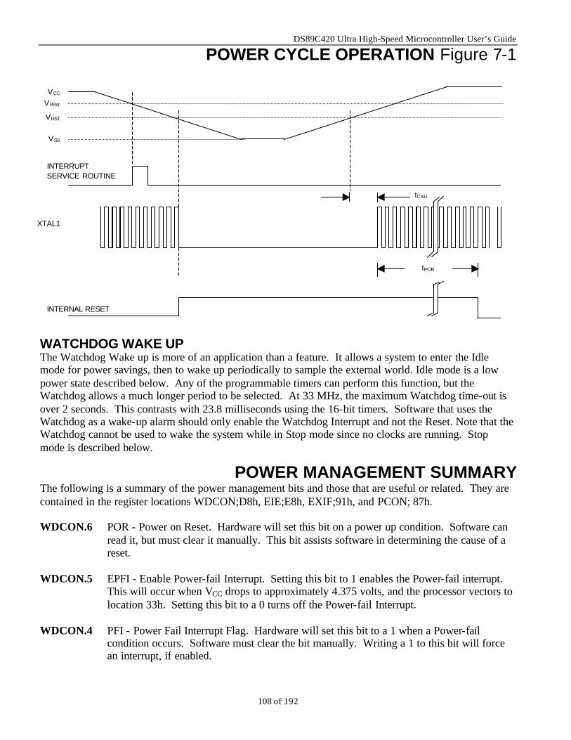
DS89C420 Ultra High-Speed Microcontroller User’s Guide
108 of 192
POWER CYCLE OPERATION Figure 7-1 WATCHDOG WAKE UP The Watchdog Wake up is more of an application than a feature. It allows a system to enter the Idle mode for power savings, then to wake up periodically to sample the external world. Idle mode is a low power state described below. Any of the programmable timers can perform this function, but the Watchdog allows a much longer period to be selected. At 33 MHz, the maximum Watchdog time-out is over 2 seconds. This contrasts with 23.8 milliseconds using the 16-bit timers. Software that uses the Watchdog as a wake-up alarm should only enable the Watchdog Interrupt and not the Reset. Note that the Watchdog cannot be used to wake the system while in Stop mode since no clocks are running. Stop mode is described below.
POWER MANAGEMENT SUMMARY The following is a summary of the power management bits and those that are useful or related. They are contained in the register locations WDCON;D8h, EIE;E8h, EXIF;91h, and PCON; 87h. WDCON.6 POR - Power on Reset. Hardware will set this bit on a power up condition. Software can
read it, but must clear it manually. This bit assists software in determining the cause of a reset.
WDCON.5 EPFI - Enable Power-fail Interrupt. Setting this bit to 1 enables the Power-fail interrupt.
This will occur when VCC drops to approximately 4.375 volts, and the processor vectors to location 33h. Setting this bit to a 0 turns off the Power-fail Interrupt.
WDCON.4 PFI - Power Fail Interrupt Flag. Hardware will set this bit to a 1 when a Power-fail
condition occurs. Software must clear the bit manually. Writing a 1 to this bit will force an interrupt, if enabled.
VCC
VPFW
VRST
VSS
INTERRUPT SERVICE ROUTINE
INTERNAL RESET
XTAL1
tPOR
tCSU
DS89C420 Ultra High-Speed Microcontroller User’s Guide
109 of 192
WDCON.3 WDIF - Watchdog Interrupt Flag. If the Watchdog Interrupt is enabled (EIE.4), hardware will set this bit to indicate that the Watchdog Interrupt has occurred. If the interrupt is not enabled, this bit indicates that the time-out has passed. If the Watchdog Reset is enabled (WDCON.1), the user has 512 system clocks to strobe the Watchdog prior to a reset. Software or any reset can clear this flag.
WDCON.2 WTRF - Watchdog Timer Reset Flag. Hardware will set this bit when the Watchdog
Timer causes a reset. Software can read it, but must clear it manually. A Power-fail Reset will also clear the bit. This bit assists software in determining the cause of a reset. If EWT=0, the Watchdog Timer will have no affect on this bit.
WDCON.1 EWT - Enable Watchdog Timer Reset. Setting this bit will turn on the Watchdog Timer
Reset function. The Interrupt will not occur unless the EWDI bit in the EIE register is set. A reset will occur according to the WD1 and WD0 bits in the CKCON register. Setting this bit to a 0 will disable the reset but leave the timer running.
WDCON.0 RWT - Reset Watchdog Timer. This bit serves as the strobe for the Watchdog function.
During the time-out period, software must set the RWT bit if the Watchdog is enabled. Failing to set the RWT will cause a reset when the time-out has elapsed. There is no need to set the RWT bit to a 0 because it is self-clearing.
EIE.4 EWDI - Enable Watchdog Interrupt. Setting this bit in software enables the Watchdog
Interrupt. EXIF.0 BGS - Band-Gap Select. Setting this bit to a 1 will allow the use of the Band-gap voltage
reference while in Stop mode. Since this function uses as much as 75 µA, the band-gap is optional in Stop mode. Setting this bit to a 0 will turn off the Band-gap while in Stop mode. When BGS=0, no Power-fail interrupt or Power-fail Reset will be available in Stop mode.
PCON.1 STOP. When this bit is set, the program stops execution, clocks are stopped, and the CPU
enters power-down mode. PCON.0 IDLE. Program execution halts leaving timers, serial ports, and clocks running. EXIF.2 RGMD - Ring Oscillator Mode. Hardware will set this status bit to a 1 when the clock
source is the Ring Oscillator. Hardware will set this status bit to a 0 when the crystal is the clock source. Refer to RGSL below for operation of the Ring Oscillator.
EXIF.1 RGSL - Ring Oscillator Select. When set to a 1 by software, the DS89C420 will use a
Ring Oscillator to come out of Stop mode without waiting for crystal start-up. This allows an instantaneous start-up when coming out of Stop mode. It is useful if software needs to perform a short task, then return to Stop. It is also useful if software must respond quickly to an external event. After the crystal has performed 65,536 cycles, hardware will switch to the crystal as its clock source. The RGMD status bit reports on this changeover. When RGSL is set to a 0, the DS89C420 will delay software execution until after the 65,536 clock crystal startup time. RGSL is only cleared by a power-on reset and is not altered by other forms of reset.
DS89C420 Ultra High-Speed Microcontroller User’s Guide
110 of 192
POWER SAVING The DS89C420 is implemented using full CMOS circuitry for low power operation. It is fully static so the clock speed can be run down to DC. Like other CMOS, the power consumption is also a function of operating frequency. Although the DS89C420 is designed for maximum performance, it also provides improved power versus work relationships compared with standard 8051 devices. These topics are discussed in detail below. CLOCK DIVIDE CONTROL The programmable Clock Divide Control bits CD1 and CD0 (PMR, C4h) provide the processor with the ability to adapt to different crystals and also to slow the system clocks providing lower power operation when required. An on-chip crystal multiplier allows the DS89C420 to operate at two or four times the crystal frequency by setting the 4X/ X2 bit and is enabled by setting the CTM bit to a logic 1. An additional circuit provides a clock source at divide by 1024. When used with a 10 MHz crystal, for example, the processor executes machine cycle in times ranging from 25 ns (divide by 0.25) to 102.4 µs (divide by 1024) and maintains a highly accurate serial port baud rate while allowing the use of more cost effective lower frequency crystals. Although the Clock Divide Control bits may be written at any time, certain hardware features have been provided to enhance the use of these clock controls to guarantee proper serial port operation, and also to allow for a high speed response to an external interrupt. The 01b setting of CD1 and CD0 is reserved, and has the same effect as the setting of 10b which forces the system clock into a divide by 1 mode. The DS89C420 defaults to divide by 1 clock mode on all forms of reset. When programmed to the divide by 1024 mode, and the switchback bit (PMR.5: SWB) is also set, the system forces the Clock Divide Control bits to reset automatically to the divide by 1 mode whenever the system has detected externally enabled interrupts. The oscillator divide ratios of 0.25, 0.5 and 1 are also used to provide standard baud rate generation for the serial ports through a forced divide by 12 input clock (TxMH,TxM = 00b, x = 1, 2, or 3) to the timers. When in divide by 1024 mode, in order to allow a quick response to incoming data on a serial port, the system utilizes the switchback mode to automatically revert to divide by 1 mode whenever a start bit is detected. This automatic switchback is only enabled during divide by 1024 mode and all other clock modes are unaffected by interrupts and serial port activity. See Power Management Mode for more details. Use of the divide by 0.25 or 0.5 option via the Clock Divide Control bits requires that the Crystal Multiplier be enabled and the specific system clock multiply value be established by the 4X/ X2 bit in the PMR register. The Multiplier is enabled via the CTM (PMR.4) bit but cannot be automatically selected until a start-up delay has been established via the CKRY bit in the status register. The 4X/ X2 bit can only be altered when the CTM bit is cleared to a logic 0. This prevents the system from changing the multiplier until the system has moved back to the divide by 1 mode and the multiplier has been disabled via the CTM bit. The CTM bit can only be altered when the CD1 and CD0 bits are set to divide by 1 mode and the RGMD bit is cleared to 0. Setting the CTM to a logic 1 from a previous logic 0 automatically clears the CKRY bit in the status register and starts the multiplier start-up time-out in the multiplier start-up counter. During the multiplier start-up period the CKRY bit will remain cleared and the CD1 and CD0 clock controls cannot be set to 00b. The CTM bit is cleared to a logic 0 on all resets. Figure 8 “System Clock sources” gives a simplified description of the generation of the system clocks. Specifics of hardware restrictions associated with the use of the 4X/ X2 CTM, CKRY, CD1 and CD0 bits are outlined in the SFR description.
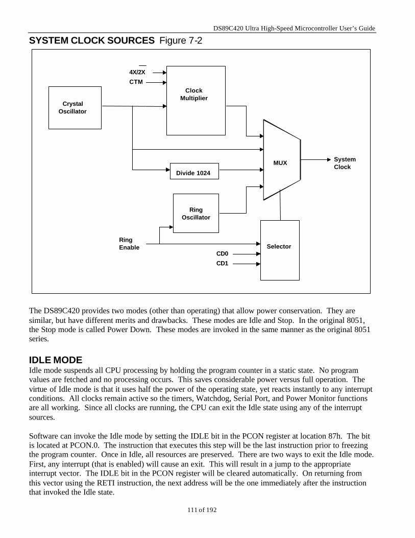
DS89C420 Ultra High-Speed Microcontroller User’s Guide
111 of 192
SYSTEM CLOCK SOURCES Figure 7-2
4X/2X
CTM
CrystalOscillator
Divide 1024
RingOscillator
ClockMultiplier
CD0
CD1
SelectorRingEnable
MUX SystemClock
The DS89C420 provides two modes (other than operating) that allow power conservation. They are similar, but have different merits and drawbacks. These modes are Idle and Stop. In the original 8051, the Stop mode is called Power Down. These modes are invoked in the same manner as the original 8051 series. IDLE MODE Idle mode suspends all CPU processing by holding the program counter in a static state. No program values are fetched and no processing occurs. This saves considerable power versus full operation. The virtue of Idle mode is that it uses half the power of the operating state, yet reacts instantly to any interrupt conditions. All clocks remain active so the timers, Watchdog, Serial Port, and Power Monitor functions are all working. Since all clocks are running, the CPU can exit the Idle state using any of the interrupt sources. Software can invoke the Idle mode by setting the IDLE bit in the PCON register at location 87h. The bit is located at PCON.0. The instruction that executes this step will be the last instruction prior to freezing the program counter. Once in Idle, all resources are preserved. There are two ways to exit the Idle mode. First, any interrupt (that is enabled) will cause an exit. This will result in a jump to the appropriate interrupt vector. The IDLE bit in the PCON register will be cleared automatically. On returning from this vector using the RETI instruction, the next address will be the one immediately after the instruction that invoked the Idle state.
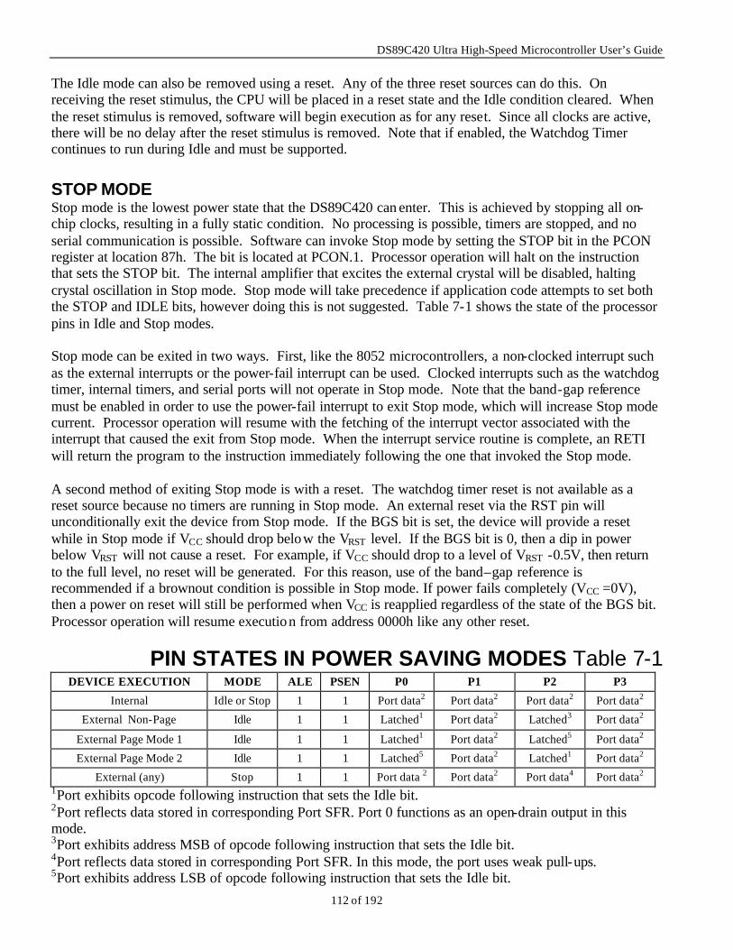
DS89C420 Ultra High-Speed Microcontroller User’s Guide
112 of 192
The Idle mode can also be removed using a reset. Any of the three reset sources can do this. On receiving the reset stimulus, the CPU will be placed in a reset state and the Idle condition cleared. When the reset stimulus is removed, software will begin execution as for any reset. Since all clocks are active, there will be no delay after the reset stimulus is removed. Note that if enabled, the Watchdog Timer continues to run during Idle and must be supported.
STOP MODE Stop mode is the lowest power state that the DS89C420 can enter. This is achieved by stopping all on-chip clocks, resulting in a fully static condition. No processing is possible, timers are stopped, and no serial communication is possible. Software can invoke Stop mode by setting the STOP bit in the PCON register at location 87h. The bit is located at PCON.1. Processor operation will halt on the instruction that sets the STOP bit. The internal amplifier that excites the external crystal will be disabled, halting crystal oscillation in Stop mode. Stop mode will take precedence if application code attempts to set both the STOP and IDLE bits, however doing this is not suggested. Table 7-1 shows the state of the processor pins in Idle and Stop modes. Stop mode can be exited in two ways. First, like the 8052 microcontrollers, a non-clocked interrupt such as the external interrupts or the power-fail interrupt can be used. Clocked interrupts such as the watchdog timer, internal timers, and serial ports will not operate in Stop mode. Note that the band-gap reference must be enabled in order to use the power-fail interrupt to exit Stop mode, which will increase Stop mode current. Processor operation will resume with the fetching of the interrupt vector associated with the interrupt that caused the exit from Stop mode. When the interrupt service routine is complete, an RETI will return the program to the instruction immediately following the one that invoked the Stop mode. A second method of exiting Stop mode is with a reset. The watchdog timer reset is not available as a reset source because no timers are running in Stop mode. An external reset via the RST pin will unconditionally exit the device from Stop mode. If the BGS bit is set, the device will provide a reset while in Stop mode if VCC should drop below the VRST level. If the BGS bit is 0, then a dip in power below VRST will not cause a reset. For example, if VCC should drop to a level of VRST -0.5V, then return to the full level, no reset will be generated. For this reason, use of the band–gap reference is recommended if a brownout condition is possible in Stop mode. If power fails completely (VCC =0V), then a power on reset will still be performed when VCC is reapplied regardless of the state of the BGS bit. Processor operation will resume execution from address 0000h like any other reset.
PIN STATES IN POWER SAVING MODES Table 7-1 DEVICE EXECUTION MODE ALE PSEN P0 P1 P2 P3
Internal Idle or Stop 1 1 Port data2 Port data2 Port data2 Port data2
External Non-Page Idle 1 1 Latched1 Port data2 Latched3 Port data2
External Page Mode 1 Idle 1 1 Latched1 Port data2 Latched5 Port data2
External Page Mode 2 Idle 1 1 Latched5 Port data2 Latched1 Port data2
External (any) Stop 1 1 Port data 2 Port data2 Port data4 Port data2 1Port exhibits opcode following instruction that sets the Idle bit. 2Port reflects data stored in corresponding Port SFR. Port 0 functions as an open-drain output in this mode. 3Port exhibits address MSB of opcode following instruction that sets the Idle bit. 4Port reflects data stored in corresponding Port SFR. In this mode, the port uses weak pull-ups. 5Port exhibits address LSB of opcode following instruction that sets the Idle bit.
DS89C420 Ultra High-Speed Microcontroller User’s Guide
113 of 192
RING OSCILLATOR WAKE UP FROM STOP A typical low power application is to keep the processor in Stop mode most of the time. Periodically, the system will wake up (using an external interrupt), take a reading of some condition, then return to sleep. The duration of full power operation is as short as possible. One disadvantage to this method is that the clock must be restarted prior to performing a meaningful operation. This start-up period is a waste of time and power since no work can be performed. The DS89C420 provides an alternative. If the Ring Select (RGSL) is enabled, the DS89C420 can exit Stop mode running from an internal Ring Oscillator. Upon receipt of an interrupt, this oscillator can start instantaneously, allowing software execution to begin immediately while the oscillator is stabilizing. Ring oscillator execution cannot be used to support accurate baud rate generation or precise timer/counter operations. Once 65,536 clock cycles have been detected, the CPU will automatically switch to the normal oscillator as its clock source. However, if the required interrupt response is very short, the software can re-enter Stop mode before the crystal is even stable. In this case, Stop mode can be invoked and both oscillators will be stopped. SPEED REDUCTION The DS89C420 is a fully CMOS 8051 compatible microcontroller. It can use significantly less power than other 8051 versions because it is more efficient. As an average, software will run 10 times faster on the DS89C420 than on other 8051 derivatives. Thus the same job can be accomplished by slowing down the crystal by a factor of 10. For example, an existing 8051 design that runs at 12 MHz can run at approximately 1.2 MHz on the DS89C420. At this reduced speed, the Ultra High-Speed Microcontroller will have lower power consumption than an 8051, yet perform the same job. Using the 10X factor, Table 7-2 shows the approximate speed at which the DS89C420 can accomplish the same work as an 8051. The exact improvement will vary depending on the actual instruction mix. Available crystal speeds must also be considered. Refer to Section 14 for information on instruction timing.
CRYSTAL VS MIPS COMPARISON Table 7-2 ORIGINAL 8051
CRYSTAL SPEED
MIPS DS89C420
CRYSTAL SPEED 16 MHz 1.3 1.6 MHz 20 MHz 1.6 2 MHz 24 MHz 2.0 2.4 MHz 33 MHz 2.7 3.3 MHz 40 MHz 3.3 4 MHz
POWER MANAGEMENT MODES Power consumption in CMOS microcontrollers is a function of operating frequency. The Power Management Mode (PMM) feature, available with the DS89C420, allows software to dynamically match operating frequency and current consumption with the need for processing power. Instead of the default one clock per machine cycle, PMM utilizes 1024 clocks per cycle to conserve power. A number of special features have been added to enhance the function of the PMM. The switchback feature allows the device to almost instantaneously return to divide by 1 mode upon detection of an enabled external interrupt or the receipt of a falling edge on a serial port receiver pin. The advantages of this become apparent when one calculates the increased interrupt service time of a device operating in PMM. In addition, a device operating in PMM would normally be unable to sample an incoming serial transmission to properly receive it. The switchback feature, explained below, allows a device to return to
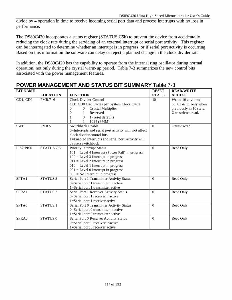
DS89C420 Ultra High-Speed Microcontroller User’s Guide
114 of 192
divide by 4 operation in time to receive incoming serial port data and process interrupts with no loss in performance. The DS89C420 incorporates a status register (STATUS;C5h) to prevent the device from accidentally reducing the clock rate during the servicing of an external interrupt or serial port activity. This register can be interrogated to determine whether an interrupt is in progress, or if serial port activity is occurring. Based on this information the software can delay or reject a planned change in the clock divider rate. In addition, the DS89C420 has the capability to operate from the internal ring oscillator during normal operation, not only during the crystal warm-up period. Table 7-3 summarizes the new control bits associated with the power management features. POWER MANAGEMENT AND STATUS BIT SUMMARY Table 7-3 BIT NAME
LOCATION FUNCTION
RESET STATE
READ/WRITE ACCESS
CD1, CD0 PMR.7–6 Clock Divider Control CD1 CD0 Osc Cycles per System Clock Cycle 0 0 Crystal Multiplier 0 1 Reserved 1 0 1 (reset default) 1 1 1024 (PMM)
10 Write: 10 anytime; 00, 01 & 11 only when previously in 10 state. Unrestricted read.
SWB PMR.5 Switchback Enable 0=Interrupts and serial port activity will not affect clock divider control bits 1=Enabled Interrupts and serial port activity will cause a switchback
0 Unrestricted
PIS2:PIS0 STATUS.7:5 Priority Interrupt Status 101 = Level 4 Interrupt (Power Fail) in progress 100 = Level 3 Interrupt in progress 011 = Level 2 Interrupt in progress 010 = Level 1 Interrupt in progress 001 = Level 0 Interrupt in progress 000 = No Interrupt in progress
0 Read Only
SPTA1 STATUS.3 Serial Port 1 Transmitter Activity Status 0=Serial port 1 transmitter inactive 1=Serial port 1 transmitter active
0 Read Only
SPRA1 STATUS.2 Serial Port 1 Receiver Activity Status 0=Serial port 1 receiver inactive 1=Serial port 1 receiver active
0 Read Only
SPTA0 STATUS.1 Serial Port 0 Transmitter Activity Status 0=Serial port 0 transmitter inactive 1=Serial port 0 transmitter active
0 Read Only
SPRA0 STATUS.0 Serial Port 0 Receiver Activity Status 0=Serial port 0 receiver inactive 1=Serial port 0 receiver active
0 Read Only
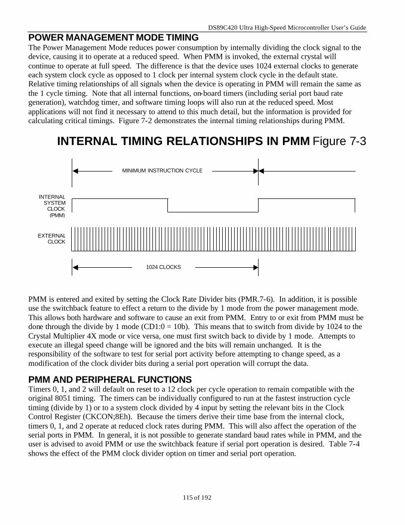
DS89C420 Ultra High-Speed Microcontroller User’s Guide
115 of 192
POWER MANAGEMENT MODE TIMING The Power Management Mode reduces power consumption by internally dividing the clock signal to the device, causing it to operate at a reduced speed. When PMM is invoked, the external crystal will continue to operate at full speed. The difference is that the device uses 1024 external clocks to generate each system clock cycle as opposed to 1 clock per internal system clock cycle in the default state. Relative timing relationships of all signals when the device is operating in PMM will remain the same as the 1 cycle timing. Note that all internal functions, on-board timers (including serial port baud rate generation), watchdog timer, and software timing loops will also run at the reduced speed. Most applications will not find it necessary to attend to this much detail, but the information is provided for calculating critical timings. Figure 7-2 demonstrates the internal timing relationships during PMM.
INTERNAL TIMING RELATIONSHIPS IN PMM Figure 7-3 PMM is entered and exited by setting the Clock Rate Divider bits (PMR.7-6). In addition, it is possible use the switchback feature to effect a return to the divide by 1 mode from the power management mode. This allows both hardware and software to cause an exit from PMM. Entry to or exit from PMM must be done through the divide by 1 mode (CD1:0 = 10b). This means that to switch from divide by 1024 to the Crystal Multiplier 4X mode or vice versa, one must first switch back to divide by 1 mode. Attempts to execute an illegal speed change will be ignored and the bits will remain unchanged. It is the responsibility of the software to test for serial port activity before attempting to change speed, as a modification of the clock divider bits during a serial port operation will corrupt the data.
PMM AND PERIPHERAL FUNCTIONS Timers 0, 1, and 2 will default on reset to a 12 clock per cycle operation to remain compatible with the original 8051 timing. The timers can be individually configured to run at the fastest instruction cycle timing (divide by 1) or to a system clock divided by 4 input by setting the relevant bits in the Clock Control Register (CKCON;8Eh). Because the timers derive their time base from the internal clock, timers 0, 1, and 2 operate at reduced clock rates during PMM. This will also affect the operation of the serial ports in PMM. In general, it is not possible to generate standard baud rates while in PMM, and the user is advised to avoid PMM or use the switchback feature if serial port operation is desired. Table 7-4 shows the effect of the PMM clock divider option on timer and serial port operation.
INTERNAL SYSTEM
CLOCK (PMM)
MINIMUM INSTRUCTION CYCLE
EXTERNAL CLOCK
1024 CLOCKS CYCLES
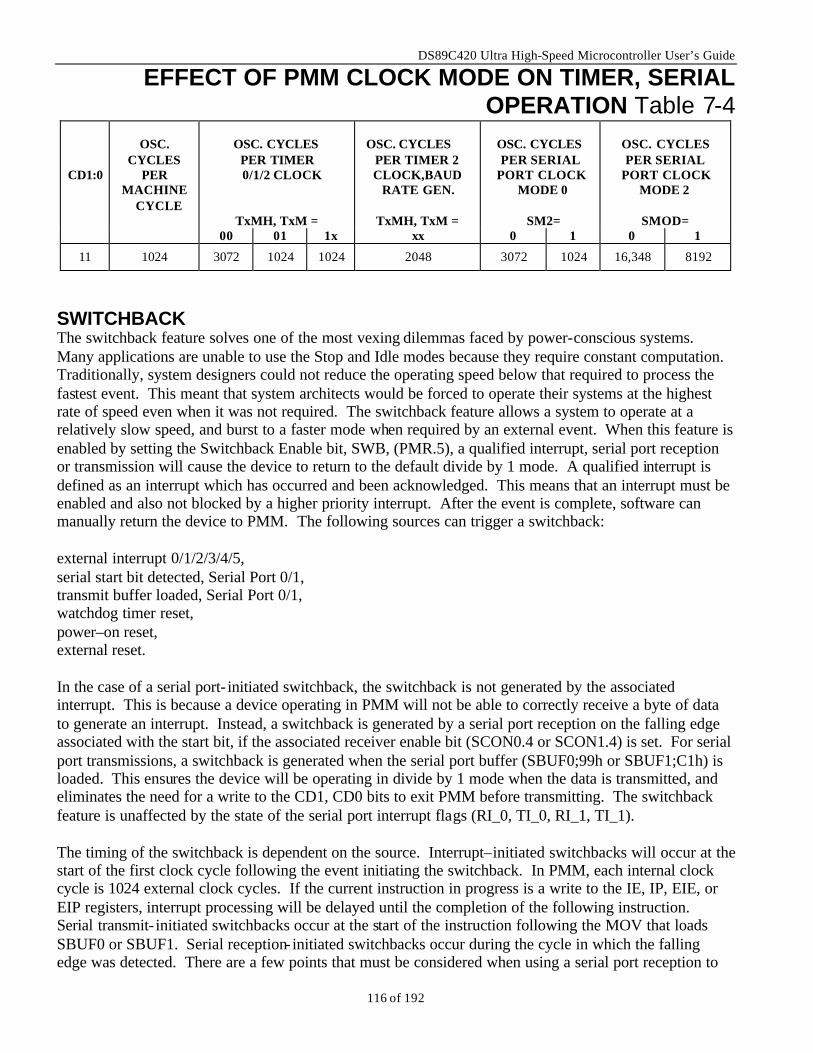
DS89C420 Ultra High-Speed Microcontroller User’s Guide
116 of 192
EFFECT OF PMM CLOCK MODE ON TIMER, SERIAL OPERATION Table 7-4
CD1:0
OSC.
CYCLES PER
MACHINE CYCLE
OSC. CYCLES
PER TIMER 0/1/2 CLOCK
TxMH, TxM =
OSC. CYCLES
PER TIMER 2 CLOCK,BAUD
RATE GEN.
TxMH, TxM =
OSC. CYCLES PER SERIAL
PORT CLOCK MODE 0
SM2=
OSC. CYCLES PER SERIAL
PORT CLOCK MODE 2
SMOD=
00 01 1x xx 0 1 0 1
11 1024 3072 1024 1024 2048 3072 1024 16,348 8192
SWITCHBACK The switchback feature solves one of the most vexing dilemmas faced by power-conscious systems. Many applications are unable to use the Stop and Idle modes because they require constant computation. Traditionally, system designers could not reduce the operating speed below that required to process the fastest event. This meant that system architects would be forced to operate their systems at the highest rate of speed even when it was not required. The switchback feature allows a system to operate at a relatively slow speed, and burst to a faster mode when required by an external event. When this feature is enabled by setting the Switchback Enable bit, SWB, (PMR.5), a qualified interrupt, serial port reception or transmission will cause the device to return to the default divide by 1 mode. A qualified interrupt is defined as an interrupt which has occurred and been acknowledged. This means that an interrupt must be enabled and also not blocked by a higher priority interrupt. After the event is complete, software can manually return the device to PMM. The following sources can trigger a switchback: external interrupt 0/1/2/3/4/5, serial start bit detected, Serial Port 0/1, transmit buffer loaded, Serial Port 0/1, watchdog timer reset, power–on reset, external reset. In the case of a serial port- initiated switchback, the switchback is not generated by the associated interrupt. This is because a device operating in PMM will not be able to correctly receive a byte of data to generate an interrupt. Instead, a switchback is generated by a serial port reception on the falling edge associated with the start bit, if the associated receiver enable bit (SCON0.4 or SCON1.4) is set. For serial port transmissions, a switchback is generated when the serial port buffer (SBUF0;99h or SBUF1;C1h) is loaded. This ensures the device will be operating in divide by 1 mode when the data is transmitted, and eliminates the need for a write to the CD1, CD0 bits to exit PMM before transmitting. The switchback feature is unaffected by the state of the serial port interrupt flags (RI_0, TI_0, RI_1, TI_1). The timing of the switchback is dependent on the source. Interrupt–initiated switchbacks will occur at the start of the first clock cycle following the event initiating the switchback. In PMM, each internal clock cycle is 1024 external clock cycles. If the current instruction in progress is a write to the IE, IP, EIE, or EIP registers, interrupt processing will be delayed until the completion of the following instruction. Serial transmit- initiated switchbacks occur at the start of the instruction following the MOV that loads SBUF0 or SBUF1. Serial reception- initiated switchbacks occur during the cycle in which the falling edge was detected. There are a few points that must be considered when using a serial port reception to
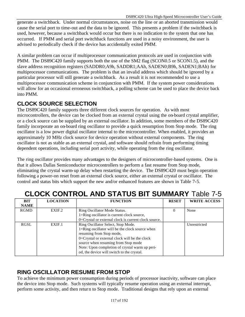
DS89C420 Ultra High-Speed Microcontroller User’s Guide
117 of 192
generate a switchback. Under normal circumstances, noise on the line or an aborted transmission would cause the serial port to time-out and the data to be ignored. This presents a problem if the switchback is used, however, because a switchback would occur but there is no indication to the system that one has occurred. If PMM and serial port switchback functions are used in a noisy environment, the user is advised to periodically check if the device has accidentally exited PMM. A similar problem can occur if multiprocessor communication protocols are used in conjunction with PMM. The DS89C420 family supports both the use of the SM2 flag (SCON0.5 or SCON1.5), and the slave address recognition registers (SADDR0;A9h, SADDR1;AAh, SADEN0;B9h, SADEN1;BAh) for multiprocessor communications. The problem is that an invalid address which should be ignored by a particular processor will still generate a switchback. As a result it is not recommended to use a multiprocessor communication scheme in conjunction with PMM. If the system power considerations will allow for an occasional erroneous switchback, a polling scheme can be used to place the device back into PMM.
CLOCK SOURCE SELECTION The DS89C420 family supports three different clock sources for operation. As with most microcontrollers, the device can be clocked from an external crystal using the on-board crystal amplifier, or a clock source can be supplied by an external oscillator. In addition, some members of the DS89C420 family incorporate an on-board ring oscillator to provide a quick resumption from Stop mode. The ring oscillator is a low power digital oscillator internal to the microcontroller. When enabled, it provides an approximately 10 MHz clock source for device operation without external components. The ring oscillator is not as stable as an external crystal, and software should refrain from performing timing dependent operations, including serial port activity, while operating from the ring oscillator. The ring oscillator provides many advantages to the designers of microcontroller-based systems. One is that it allows Dallas Semiconductor microcontrollers to perform a fast resume from Stop mode, eliminating the crystal warm-up delay when restarting the device. The DS89C420 must begin operation following a power-on reset from an external clock source, either an external crystal or oscillator. The control and status bits which support the new and/or enhanced features are shown in Table 7-5.
CLOCK CONTROL AND STATUS BIT SUMMARY Table 7-5 BIT
NAME LOCATION FUNCTION RESET WRITE ACCESS
RGMD EXIF.2 Ring Oscillator Mode Status. 1=Ring oscillator is current clock source, 0=Crystal or external clock is current clock source.
0 None
RGSL EXIF.1 Ring Oscillator Select, Stop Mode. 1=Ring oscillator will be the clock source when resuming from Stop mode, 0=Crystal or external clock will be the clock source when resuming from Stop mode Note: Upon completion of crystal warm up peri-od, the device will switch to the crystal.
Unrestricted
RING OSCILLATOR RESUME FROM STOP To achieve the minimum power consumption during periods of processor inactivity, software can place the device into Stop mode. Such systems will typically resume operation using an external interrupt, perform some activity, and then return to Stop mode. Traditional designs that rely upon an external
DS89C420 Ultra High-Speed Microcontroller User’s Guide
118 of 192
crystal as the clock source must incur the startup delay of the crystal when resuming from Stop mode. This is a waste of time and power as no work can be performed until the crystal has stabilized. Although the ring oscillator provides an approximately 10 MHz clock source for device operation, it is not as stable as an external crystal. As a result, high accuracy timing operations should be avoided while running from the ring oscillator. This includes using the timers for pulse measurement, and the use of the serial ports in asynchronous modes (1, 2, 3). Serial ports operating in mode 0 are unaffected by the stability of the clock source as a separate synchronizing clock is generated. If the Ring Oscillator Select bit, RGSL (EXIF.1) is set, the device will resume operation immediately using the internal ring oscillator as the clock source. The device will continue to run from the ring oscillator until the crystal warm-up period of 65,536 clock cycles (measured from the external source) has completed. At this time the device will switch to the clock source active before it entered Stop mode and continue operation. This allows software execution to begin immediately upon resuming from Stop mode. The current clock source is indicated by the Ring Oscillator Mode bit, RGMD (EXIF.2). In Stop mode, enabled interrupts become true edge triggered interrupts, compared with the sampled edge detection used during normal operation. This means that external interrupts are more sensitive to noise in Stop mode than during normal operation. Applications should be carefully designed to ensure that noise will not cause an erroneous exit from Stop mode.
DS89C420 Ultra High-Speed Microcontroller User’s Guide
119 of 192
SECTION 8: RESET CONDITIONS A condition that causes the DS89C420 CPU to vector to address 0000h is a reset. This can happen internally or external to the microcontroller. The reset condition puts the microcontroller in a known state following a course of events not anticipated by the designer. The circuit could be subjected to numerous conditions, such as power brown-out, noise due to lightning strike, or corrupted code. RESET SOURCES The DS89C420 can enter a reset condition if invoked by one of four ways. These conditions are: Power-on/Power Fail Reset Watchdog Timer Reset Oscillator Fail Detect Reset Internal System Reset External Reset The reset state of the DS89C420 will be the same, regardless of the source of the reset. When in reset, the oscillator is running, but no program execution is allowed. When the reset source is external, the user must remove the reset stimulus to continue operation. When power is applied to the device, the power on delay removes the stimulus automatically. POWER-ON/POWER FAIL RESET The DS89C420 incorporates an internal voltage reference, which holds the device in power-on reset while VCC is out of tolerance. Once VCC has risen above the threshold, the DS89C420 will restart the external crystal oscillator and count 65,536 clock cycles before program execution begins at location 0000h. The power monitor will invoke a reset state when VCC drops below the threshold condition. The condition will remain in effect while power is below the minimum voltage level. When power returns above the reset threshold, a full power-on reset will be performed. This mechanism provides a controlled and predictable start-up condition. The processor exits the reset condition automatically once VCC meets the minimum voltage requirement. This helps the system maintain reliable operation by only permitting processor operation when voltage is in a known good state. Software can determine that a Power-on Reset has occurred by checking the Power-on Reset flag, POR, in the WDCON register. Software should clear the POR bit after it is read. WATCHDOG TIMER RESET The DS89C420 incorporates a safety feature to prevent corrupted software from controlling the CPU. This feature is called the Watchdog Timer. It is a free running timer with a programmable interval. The Watchdog supervises the processor operation by requiring software to clear the timer before an overflow occurs. If the timer is enabled and software fails to clear it before this interval expires, the DS89C420 is placed into a reset state. The reset state will maintain for 13 clock cycles. Once the reset is removed, the processor will resume execution at address 0000h. Software can determine if a reset is caused by a Watchdog time-out by checking the Watchdog Timer Reset flag, WTRF in the WDCON register. This flag is cleared by software only.
OSCILLATOR FAIL DETECT RESET The DS89C420 incorporates oscillator fail detect circuitry to monitor the on-chip oscillator activity. When enabled, this circuit causes a reset if the oscillator frequency falls below ~20kHz, and holds the chip in reset until the oscillator frequency rises back above ~20kHz. The circuitry is enabled by setting the OFDE (PCON.4) bit to a logic 1. The OFDE bit can be cleared by software or by the occurrence of a
DS89C420 Ultra High-Speed Microcontroller User’s Guide
120 of 192
power-fail reset. A reset caused by an oscillator failure sets the OFDF (PCON.5) flag bit to a logic 1. This flag can be cleared by software or by a power on reset. The oscillator fail detect circuitry utilizes the internal ring oscillator to clock the chip into the reset state and maintain the reset state while the oscillator is below the minimum frequency. Note, however, that the circuitry will not force a reset when the oscillator is purposely stopped when software invokes stop mode.
INTERNAL SYSTEM RESET The DS89C420 supports in-system programming. The lower on-chip memory bank can be re-programmed via a bank switch mechanism by complementing the logic state of the bank select bit and invoking a reset. An internal system reset can be initiated by writing a ‘system reset’ or ‘complement bank select’ command to the FCNTL register. The reset state will be maintained for 13 clock cycles, once the reset is removed. The on-chip memory banks will be reconfigured in an addressing order determined by the logic value of the bank select bit. At this point, the CPU will execute code from the reset vector address 0000h. EXTERNAL RESET If the RST input is asserted to logic 1, the device will be forced into a reset state. An external reset is accomplished by holding the RST pin high at least 4 clock cycles while the oscillator is running. Once the reset state is invoked, it will be maintained as long as RST is asserted at logic 1. When the RST is removed, the processor will exit the reset state within 4 clock cycles and begin execution at address 0000h. If a RST is applied while the processor is in the Stop mode, the RST will cause the oscillator to begin running and force the program counter to 0000h. The reset delay will be 65,536 clock cycles to allow the oscillator to stabilize. The RST pin is a bi-directional I/O. If a reset is caused by a Power Fail Reset, a Watchdog Timer Reset, an Oscillator Fail Detect Reset, or an Internal System Reset, a positive output level is also generated at the RST pin. This reset level is asserted as long as an internal reset is asserted. The drive capability of this I/O port may be insufficient if the RST pin is connected to a RC reset circuit. Connecting the RST pin to a capacitor would not affect the internal reset condition. DETERMINING THE CAUSE OF A RESET During the debugging process, it may be necessary to isolate the cause of a device reset. Because resets are initiated by a limited number of sources, it is relatively easy to determine their source by interrogating the flag bits associated with the reset sources. The table below lists the reset sources and flag bits. Although no flag bits are associated with the internal system reset generated by issuing a ‘system reset’ or ‘complement bank select’ flash command, it is unlikely that these would occur unintentionally given that the flash command bits (FCNTL.3-0) require a timed access write. RESET SOURCE FLAG BIT Power-on reset POR – WDCON.6 Watchdog reset WTRF – WDCON.3 Oscillator fail detect reset OFDF – PCON.5 Internal system reset None External reset None
DS89C420 Ultra High-Speed Microcontroller User’s Guide
121 of 192
SECTION 9: INTERRUPTS The Ultra High-Speed Microcontroller family improves upon the traditional 8051 architecture by utilizing a five-priority interrupt system. The five priority levels, from highest priority to lowest, are 4, 3, 2, 1, and 0. The power-fail interrupt, when enabled, always receives the highest priority (level 4), while other interrupt sources can be configured to level 3, 2, 1 or 0. Each source has independent priority bits, flag(s), interrupt vector, and enable. In addition, interrupts can be globally enabled (or disabled). The interrupt system is compatible with the original 8051 family, having all of the original interrupts available. A summary of all interrupt sources is provided in the table below.
INTERRUPT SUMMARY Table 9-1 INTERRUPT INTERRUPT
VECTOR NATURAL
ORDER FLAG ENABLE PRIORITY
CONTROL Power–fail 33h 0 (highest) PFI (WDCON.4) EPFI (WDCON.5) N/A
External Interrupt 0 03h 1 IE0 (TCON.1)** EX0 (IE.0) MPX0 (IP1.0) LPX0 (IP0.0)
Timer 0 Overflow 0Bh 2 TF0 (TCON.5)* ET0 (IE.1) MPT0 (IP1.1) LPT0 (IP0.1)
External Interrupt 1 13h 3 IE1 (TCON.3)** EX1 (IE.2) MPX1 (IP1.2) LPX1 (IP0.2)
Timer 1 Overflow 1Bh 4 TF1 (TCON.7)* ET1 (IE.3) MPT1 (IP1.3) LPT1 (IP0.3)
Serial Port 0 23h 5 RI_0 (SCON0.0), TI_0 (SCON0.1)
ES0 (IE.4) MPS0 (IP1.4) LPS0 (IP0.4)
Timer 2 Overflow 2Bh 6 TF2 (T2CON.7) EXF2(T2CON.6)
ET2 (IE.5) MPT2 (IP1.5) LPT2 (IP0.5)
Serial Port 1 3Bh 7 RI_1 (SCON1.0), TI_1 (SCON1.1)
ES1 (IE.6) MPS1 (IP1.6) LPS1 (IP0.6)
External Interrupt 2 43h 8 IE2 (EXIF.4) EX2 (EIE.0) MPX2 (EIP1.0) LPX2 (EIP0.0)
External Interrupt 3 4Bh 9 IE3 (EXIF.5) EX3 (EIE.1) MPX3 (EIP1.1) LPX3 (EIP0.1)
External Interrupt 4 53h 10 IE4 (EXIF.6) EX4 (EIE.2) MPX4 (EIP1.2) LPX4 (EIP0.2)
External Interrupt 5 5Bh 11 IE5 (EXIF.7) EX5 (EIE.3) MPX5 (EIP1.3) LPX5 (EIP0.3)
Watchdog Interrupt 63h 12 WDIF (WDCON.3)
EWDI (EIE.4) MPWDI (EIP1.4) LPWDI (EIP0.4)
Unless marked these flags must be cleared manually by software. * Cleared automatically by hardware when the service routine is vectored to. ** If edge triggered, cleared automatically by hardware when the service routine is vectored to. If level
triggered, flag follows the state of the pin.
INTERRUPT OVERVIEW An interrupt allows the software to react to unscheduled or asynchronous events. When an interrupt occurs, the CPU is expected to “service” the interrupt. This service takes the form of an Interrupt Service Routine (ISR). The ISR resides at a predetermined address as shown in Table 9-1. When the interrupt occurs, the CPU will vector to this address and run code created to service the interrupt. The CPU will stay in an interrupt service state until the ‘return from interrupt’ instruction (RETI) is executed at completion of the ISR. When a RETI is performed, the processor will return to the instruction that would have been next when the interrupt occurred. Once an ISR has begun, it can be interrupted only by a higher priority interrupt.
DS89C420 Ultra High-Speed Microcontroller User’s Guide
122 of 192
When an interrupt condition occurs, the processor will indicate this by setting a flag bit. This flag bit cannot alone cause an interrupt, and will be set regardless of whether the interrupt is enabled or not. Most flags must be cleared manually by software. However, IE0 and IE1 are cleared automatically by hardware upon vectoring to the service routine if the interrupt was edge triggered. In level triggered mode, the IE0 or IE1 flags will follow the state of the pin. Flags TF0 and TF1 are always cleared automatically when the service routine is vectored to. Refer to the individual bit descriptions for more details. Each source must be individually enabled in order to generate CPU interrupts. Each interrupt source has an independent enable as shown in Table 9-1. In order for the processor to acknowledge the interrupt and vector to the ISR, the Enable All bit (IE.7: EA) must be set to globally enable interrupt sources. Clearing the EA bit to a logic 0 disables all interrupts regardless of the individual interrupt enables. The power fail warning interrupt source is the only exception, requiring only its individual enable bit be set (WDCON.5: EPFI) to be recognized by the CPU. The EA bit has no effect on the Power-fail Interrupt.
INTERRUPT SOURCES The interrupt sources present on the Ultra High-Speed Microcontroller can broken into several categories: External, Timer-based, Serial Communication, and Power Monitor. Each type is described below. Interrupt sources are evaluated during the final memory cycle of each instruction to determine whether and which interrupt will be serviced. If the interrupt source goes active after this evaluation, it will not be considered until the final memory cycle of the next instruction.
External Interrupts The Ultra High-Speed Microcontroller has 6 external interrupt sources. These include the standard 2 interrupts of the 8051 architecture and 4 new sources. The original interrupts are INT0 and INT1. These are active low and can be programmed to be edge- or level-sensitive. The detection mode for each source is controlled through TCON register bits IT0 and IT1, respectively. When ITx=0, the interrupt is triggered by a logic 0 on the appropriate interrupt pin. The interrupt condition remains in effect as long as the pin is low. When ITx=1, the interrupt is pseudo edge-triggered. This means that, if on successive samples the pin is found to be in a low state, which would indicate that a falling edge occurred, the interrupt is activated. Since the external interrupts are sampled, the pin driver of an edge-triggered interrupt should hold both the high, then the low condition for at least two system clock cycles (each) to insure detection. This means maximum sampling frequency on any interrupt pin is 1/4 of the system clock frequency. It is important to note that level-sensitive interrupts are not latched. This is most important if using other interrupts of equal or higher priority because the level-sensitive interrupt request may not receive immediate service by the processor. A level-sensitive interrupt request will be missed unless the condition is held until it can be serviced. The remaining 4 external interrupts are similar in nature, with two differences. First, all of the four new interrupts are edge-detect only. They do not have level-detect modes. Second, INT2 and INT4 are positive edge sensitive instead of negative edge sensitive. All associated bits and flags operate the same and have the same polarity as the original two. A logic 1 indicates the presence of a condition, not the logic state of the pin. If the Power Management Mode is utilized, the designer must remember that detection of edge triggered interrupts is defined in relation to the system clock (=1024 oscillator clock cycles). This means that it
DS89C420 Ultra High-Speed Microcontroller User’s Guide
123 of 192
will require 2048 external clock cycles before detecting that an edge has just occurred. As a result, the latency for these interrupts will be much longer in Power Management Mode.
Timer Interrupts The DS89C420 incorporates three 16-bit programmable timers, each of which can generate an interrupt, and a programmable watchdog timer. The three 16-bit programmable timers operate in the same manner as the 80C52. Each timer has an independent interrupt enable, flag, vector and priority. The watchdog timer also has its own interrupt enable, flag and priority. Timers 0 and 1 will set their respective interrupt flags when the timer overflows from a full condition, depending on its mode. This flag will be set regardless of the interrupt enable state. If the interrupt is enabled, this event will generate a call to the corresponding interrupt vector. For timers 0 and 1, the flags are cleared when the processor jumps to the interrupt vector. Thus, these flags are not available for use by the interrupt service routine (ISR), but are available outside of the ISR and in applications that don’t acknowledge the interrupt (i.e., jump to the vector). If the interrupt is not acknowledged, then software must manually clear the flag bit. In addition to having an interrupt flag for an overflow condition (as is the case for timers 0 and 1), timer 2 has a second interrupt flag (EXF2) that is associated with detection of a falling edge on the T2EX (P1.1) pin. When timer 2 has been configured in capture mode (CP/RL2=1, EXEN2=1) or auto-reload mode (CP/RL2=0, EXEN2=1, DCEN=0), a negative transition on T2EX will cause the EXF2 interrupt flag to be set. For timer 2 interrupts, jumping to the interrupt vector does not clear either of the flags. Instead, software must ascertain which flag caused the interrupt and clear it manually. Timer 0 and 1 flag bits reside in the TCON register. Timer 2 flag bits reside in the T2CON register. The interrupt enables and priorities for timers 0, 1, and 2 reside in the IE and IP0, IP1 registers. The watchdog interrupt usually has a different connotation than the timer interrupts. Unless the watchdog is being used as a very long timer, the interrupt means that the software has failed to reset the timer and may be lost. The watchdog ISR can attempt to determine the system state or allow the CPU to be reset if the watchdog reset function has been enabled (EWT=1). Like other sources, the Watchdog Timer has a flag bit, enable bit, priority bits and its own vector.
Serial Communication Interrupts Each UART is capable of generating an interrupt. Each UART has its own interrupt enable, vector and priority. Each UART interrupt has two flags (RI, TI) that are used by the ISR to determine whether the interrupt comes from a received word or a transmitted one. Unlike the timers, the UART flags are not altered when the interrupt is serviced. Software must change them manually. When a UART finishes the transmission of a word, the TI bit will be set and an interrupt will be generated (if enabled). Likewise, the UART will set the RI bit and generate an interrupt when a word is completely received. The CPU will not be notified until the word is completely received or transmitted.
Power-fail Interrupt The Ultra High-Speed Microcontroller has the ability to generate an interrupt when VCC drops below a predetermined level. By comparing a fixed ratio of VCC versus an internal reference, the DS89C420 can assess when VCC drops below the VPFW level and cause an interrupt (if enabled). The level of VPFW is provided in the data sheet DC electrical specifications. The Power-fail interrupt is a level-sensitive condition and will remain in effect as long as VCC remains below VPFW. The Power-fail Interrupt has the highest priority level, which cannot be altered by the user. The EPFI bit solely controls the enabling or disabling of the Power-fail Interrupt source and is not subject to the global interrupt enable (EA). The EPFI bit should always be cleared to a logic 0 state if the Power-fail interrupt is not needed.
DS89C420 Ultra High-Speed Microcontroller User’s Guide
124 of 192
Simulated Interrupts Software can simulate any interrupt source by setting the corresponding flag bit. This forces an interrupt condition which will be acknowledged (if enabled) and is otherwise indistinguishable from the real thing. Thus, an interrupt flag bit should never be set to a logic 1 by software inadvertently. Once an interrupt has been acknowledged, software cannot prevent or end the interrupt by clearing its flag. If, however, software clears an interrupt flag before the interrupt is acknowledged, the interrupt will not occur.
INTERRUPT PRIORITIES The Ultra High-Speed Microcontroller has five interrupt priority levels. The five priority levels, from highest priority to lowest, are 4, 3, 2, 1 and 0. The power-fail interrupt, when enabled, always receives the highest priority (level 4), while the remaining interrupt sources can individually be programmed to level 3, 2, 1 or 0. The lowest priority (level 0) is the default condition for the other sources. An interrupt being serviced can only be interrupted by a higher priority interrupt. The power-fail interrupt source, assigned priority level 4, therefore, has the ability to interrupt the service routine of any other source. No interrupt source with equal or lesser priority to one currently being serviced can interrupt the service routine. If two interrupt sources of equal priority levels are requested simultaneously, natural priority is used to arbitrate. The natural priority is given in Table 9-1. Note that natural priority is only used to resolve simultaneous requests. Once an interrupt of a given priority is invoked, only a source that is programmed with a higher priority can intercede.
Interrupt register conflicts During normal operation there is a small but finite probability that application software may try to read or modify a register associated with interrupt functions at the same time that the interrupt hardware is modifying the register. In general, these hardware/software interrupt conflicts are resolved according to the "hardware wins" philosophy: In the event of a conflict, the hardware modification of a register will take precedence over the software action to ensure that the interrupt event is not missed.
To assist in prevention of hardware/software conflicts, the interrupt selection process that normally occurs in the final
memory cycle of each instruction is aborted for any instructions which write to the IP0, IP1, EIP0, EIP1, IE, or
EIE registers. When the evaluation takes place in the subsequent instruction, the interrupt source will
incorporate the new priority and enable values from the previous instruction. If this situation occurs, it will lengthen the interrupt latency by the length of the
instruction that modified the register.
DS89C420 Ultra High-Speed Microcontroller User’s Guide
125 of 192
INTERRUPT ACKNOWLEDGE CYCLE The process of acknowledging an interrupt begins with the setting of the associated flag. For edge triggered external interrupts and internal interrupt sources, the interrupt flags are set automatically by hardware. For level sensitive external interrupts, the flags are actually under control of the external signal, and the flag will rise and fall with the pin level. All interrupt flags are evaluated on the final execution cycle of each instruction. A priority decoding process is performed amongst pending and new interrupt sources in order to select the appropriate interrupt vector address. This decoding process is accomplished in a single memory cycle using combinatorial logic. Hardware then forces an LCALL to the selected vector address in the following memory cycle, unless blocked by one of the following conditions: 1. An interrupt of equal or greater priority has already been invoked and the RETI instruction has not
been issued to terminate it. 2. The current cycle is not the final cycle in the execution of the current instruction. 3. The instruction in progress is an RETI or a write to IP0, IP1, EIP0, EIP1, IE, or EIE.
INTERRUPT LATENCY Interrupt response time will normally be between four and eighteen memory cycles depending on the state of the microcontroller when the interrupt occurs. If the microcontroller is performing an ISR with equal or greater priority, interrupt latency will increase because the new interrupt will not be invoked. In other cases, the response time will depend on the current instruction. The fastest possible response to an interrupt is four memory cycles. The four memory cycle response time includes one cycle for detecting the interrupt and three cycles to perform the LCALL that is inherent in the interrupt request. The maximum response time occurs if the microcontroller is performing a JBC instruction that clears a bit in IE, IP0, EIE, or EIP0 and then executes a DIV as the next instruction. From the time an interrupt source is activated (not detected), the longest reaction time is eighteen memory cycles. This includes one cycle to detect the interrupt, four cycles to finish the JBC, ten cycles to perform the DIV, then three cycles for the LCALL to the ISR. This maximum response time of eighteen memory cycles assumes that there are no other pending interrupts of higher priority to be serviced and that the JBC instruction is no t preceded and does not jump to any instruction that aborts the priority decoding process (RETI or writes to IP0, IP1, EIP0, EIP1, IE, or EIE).
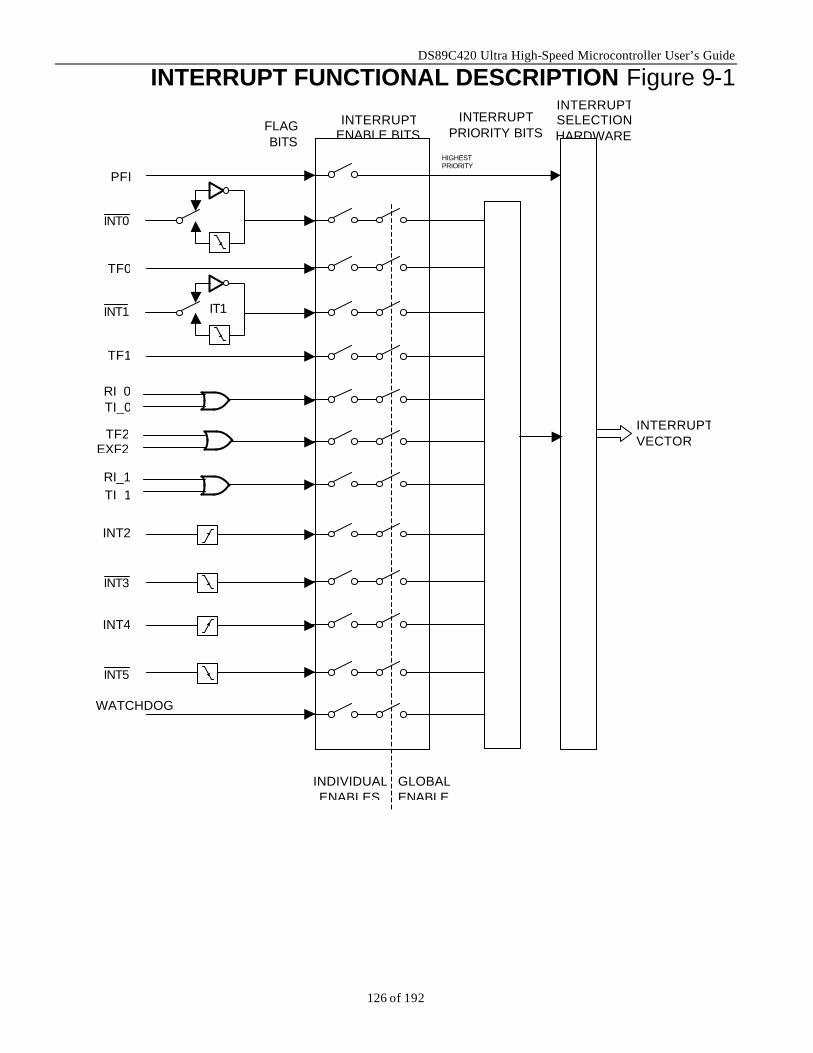
DS89C420 Ultra High-Speed Microcontroller User’s Guide
126 of 192
INTERRUPT FUNCTIONAL DESCRIPTION Figure 9-1
INTERRUPT ENABLE BITS
INTERRUPT VECTOR
INTERRUPT SELECTION HARDWARE
FLAGBITS
PFI
INT0
TF0
TF1
RI_0TI_0
RI_1TI_1
TF2EXF2
INT2
INT4
WATCHDOG
IT1
HIGHEST PRIORITY
INDIVIDUAL ENABLES
GLOBAL ENABLE
INT1
INT3
INT5
INTERRUPT PRIORITY BITS
DS89C420 Ultra High-Speed Microcontroller User’s Guide
127 of 192
SECTION 10: I/O PORTS The DS89C420 provides four 8-bit I/O ports. Each port appears as a Special Function Register that can be addressed as a byte or 8 individual bit locations. In general, the register and the port pin have identical values, and reading or writing a port is the same as reading or writing the SFR for the port. The basic I/O driver function and its electrical characteristics are similar to the drivers used in the DS87C520, with respect to individual port and pin conditions. Port 0 and port 2 can serve either as general-purpose parallel I/O ports or as the expanded memory bus. Ports 1 and 3 can be used as general-purpose parallel I/O ports with optional special functions associated with each pin. Enabling the special function for a pin automatically converts the I/O pin to that function. An optional function of a pin can be turned on and off dynamically to suit the application. Using one or more I/O pins of a port as special functions will not affect the remaining port pins. It should be noted that port 0 drivers are open-drain and require external pull-ups when used as general-purpose I/O ports. Parallel I/O Each I/O port can be used as a general-purpose bi-directional parallel I/O port. Data written to the port latch serves to set both the level and the direction of the data on the pin. The output of the port pin is established by writing to the associated port pin latch. When logic 0 is written to the port for output, the port is pulled to ground. When logic 1 is written to ports 1, 2 or 3, a strong driver will momentarily drive the pin from 0 to 1, and then a weak pull-up will maintain the 1. A logic 1 written to port 0 will cause those pins to go tri-state, functioning as open-drain outputs. A logic 1 in the port latch also configures the port pin to the input state. Since the pin is either weakly pulled up or in tri-state, the pin will be the same as the driven logic state. The logic state of the pin itself will not alter the logic value of the port latch. Port 0 This is an open-drain, 8-bit, bi-directional, general-purpose I/O port. A reset condition or logic 1, written to the latches of this port, will tri-state the port pins. This condition also serves as an input mode. When used as an I/O port, external pull-ups are required. As an alternate function, this port can be used as part of the multiplexed address/data bus to access external memory. The DS89C420 supports both non-page and page mode. During the original 8051 expanded bus configuration (non-page mode), when ALE is high, the LSB of the address is presented to P0. When ALE is low, the port transitions to a bi-directional data bus. When used in Page Mode 1, P0 is used as the primary data bus, only. When used in Page Mode 2, P0 is used for the LSB of the address, only. The use of Port 0 as general purpose I/O is not recommended if the device will be used to access external memory. In this case, the state of the pins will be disturbed during the memory access. In addition, the pull-ups required to maintain a high state during the use as general purpose I/O will interfere with the complementary drivers employed when the device operates as an expanded memory bus.
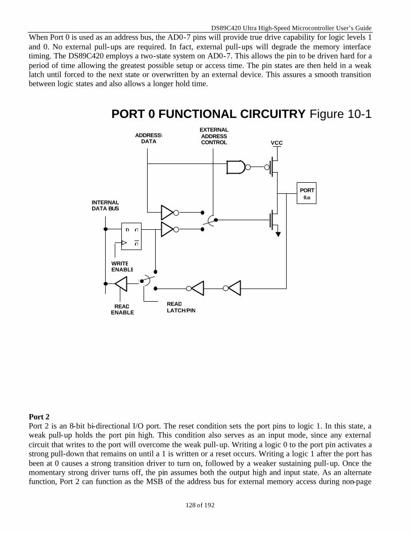
DS89C420 Ultra High-Speed Microcontroller User’s Guide
128 of 192
When Port 0 is used as an address bus, the AD0-7 pins will provide true drive capability for logic levels 1 and 0. No external pull-ups are required. In fact, external pull-ups will degrade the memory interface timing. The DS89C420 employs a two-state system on AD0-7. This allows the pin to be driven hard for a period of time allowing the greatest possible setup or access time. The pin states are then held in a weak latch until forced to the next state or overwritten by an external device. This assures a smooth transition between logic states and also allows a longer hold time.
PORT 0 FUNCTIONAL CIRCUITRY Figure 10-1
Port 2 Port 2 is an 8-bit bi-directional I/O port. The reset condition sets the port pins to logic 1. In this state, a weak pull-up holds the port pin high. This condition also serves as an input mode, since any external circuit that writes to the port will overcome the weak pull-up. Writing a logic 0 to the port pin activates a strong pull-down that remains on until a 1 is written or a reset occurs. Writing a logic 1 after the port has been at 0 causes a strong transition driver to turn on, followed by a weaker sustaining pull-up. Once the momentary strong driver turns off, the pin assumes both the output high and input state. As an alternate function, Port 2 can function as the MSB of the address bus for external memory access during non-page
ADDRESS\ DATA
EXTERNAL ADDRESS CONTROL
PORT 0.n
D Q
Q
INTERNAL DATA BUS
WRITE ENABLE
READ ENABLE
READ LATCH/PIN
VCC

DS89C420 Ultra High-Speed Microcontroller User’s Guide
129 of 192
mode. When used in Page Mode 1, P2 is used for both LSB and MSB of external address. When used in Page Mode 2, P2 is used for the MSB of external address and data.
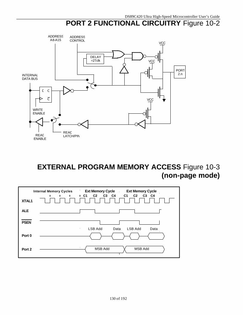
DS89C420 Ultra High-Speed Microcontroller User’s Guide
130 of 192
PORT 2 FUNCTIONAL CIRCUITRY Figure 10-2
EXTERNAL PROGRAM MEMORY ACCESS Figure 10-3 (non-page mode)
Internal Memory CyclesC2 C3 C4 C1 C2 C3 C4
XTAL1
ALE
Port 0
Port 2
PSEN
C1Ext Memory CycleExt Memory Cycle
MSB Add MSB Add
LSB Add Data LSB Add Data
ADDRESS A8-A15
ADDRESS CONTROL
D Q
Q
INTERNAL DATA BUS
WRITE ENABLE
READ ENABLE
READ LATCH/PIN
PORT 2.n
VCC
DELAY =2Tclk
VCC
VCC
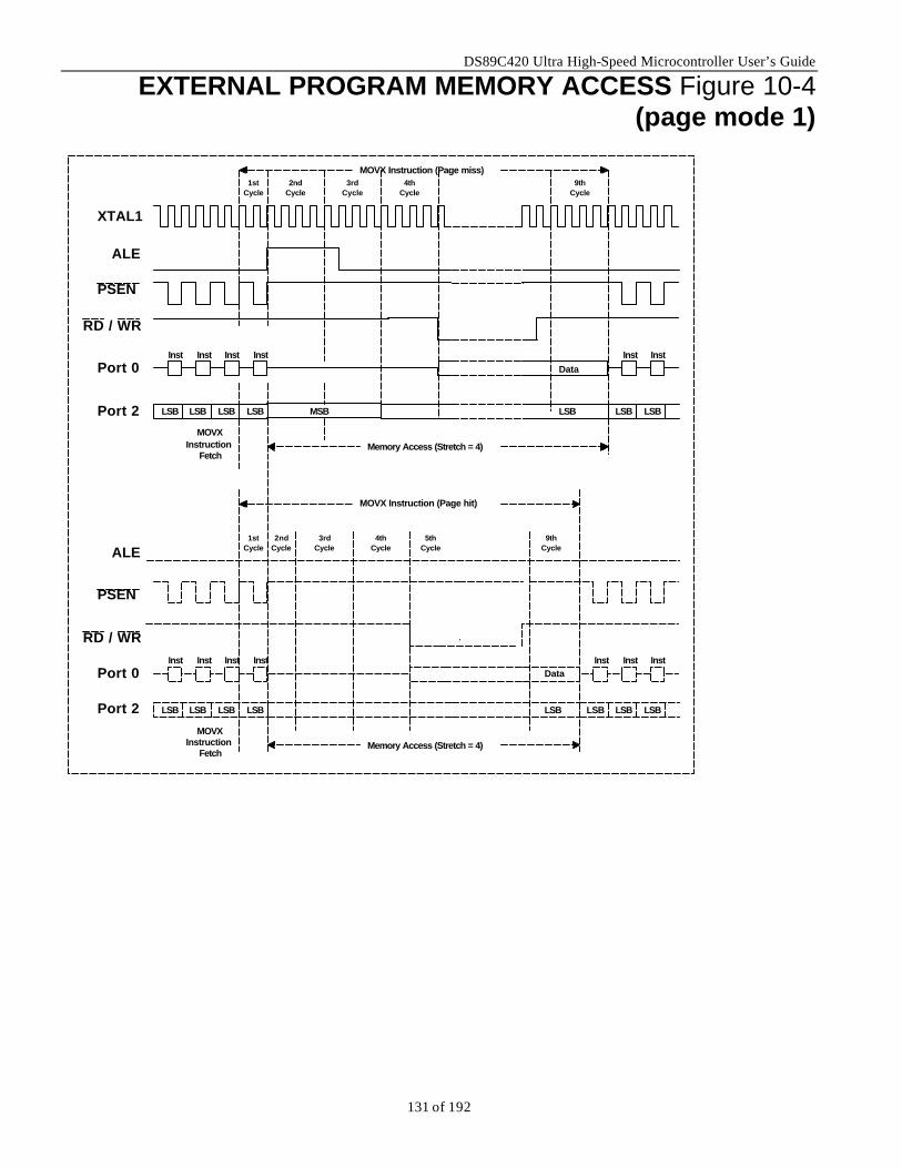
DS89C420 Ultra High-Speed Microcontroller User’s Guide
131 of 192
EXTERNAL PROGRAM MEMORY ACCESS Figure 10-4 (page mode 1)
ALE
PSEN
Port 0
Port 2
ALE
PSEN
Port 0
Port 2
RD / WR
XTAL1
InstInst Inst InstInst
MSBLSB LSB LSBLSB LSB LSB LSB
Inst
Data
Memory Access (Stretch = 4)
MOVX Instruction (Page miss)1st
Cycle2nd
Cycle3rd
Cycle4th
Cycle9th
Cycle
MOVXInstruction
Fetch
LSB LSB LSB
Inst Inst Inst
MOVX Instruction (Page hit)
Memory Access (Stretch = 4)
MOVXInstruction
Fetch
1st Cycle
2nd Cycle
3rd Cycle
4th Cycle
5th Cycle
9th Cycle
LSBLSBLSBLSB
Inst Inst Inst Inst
RD / WR
Data
LSB
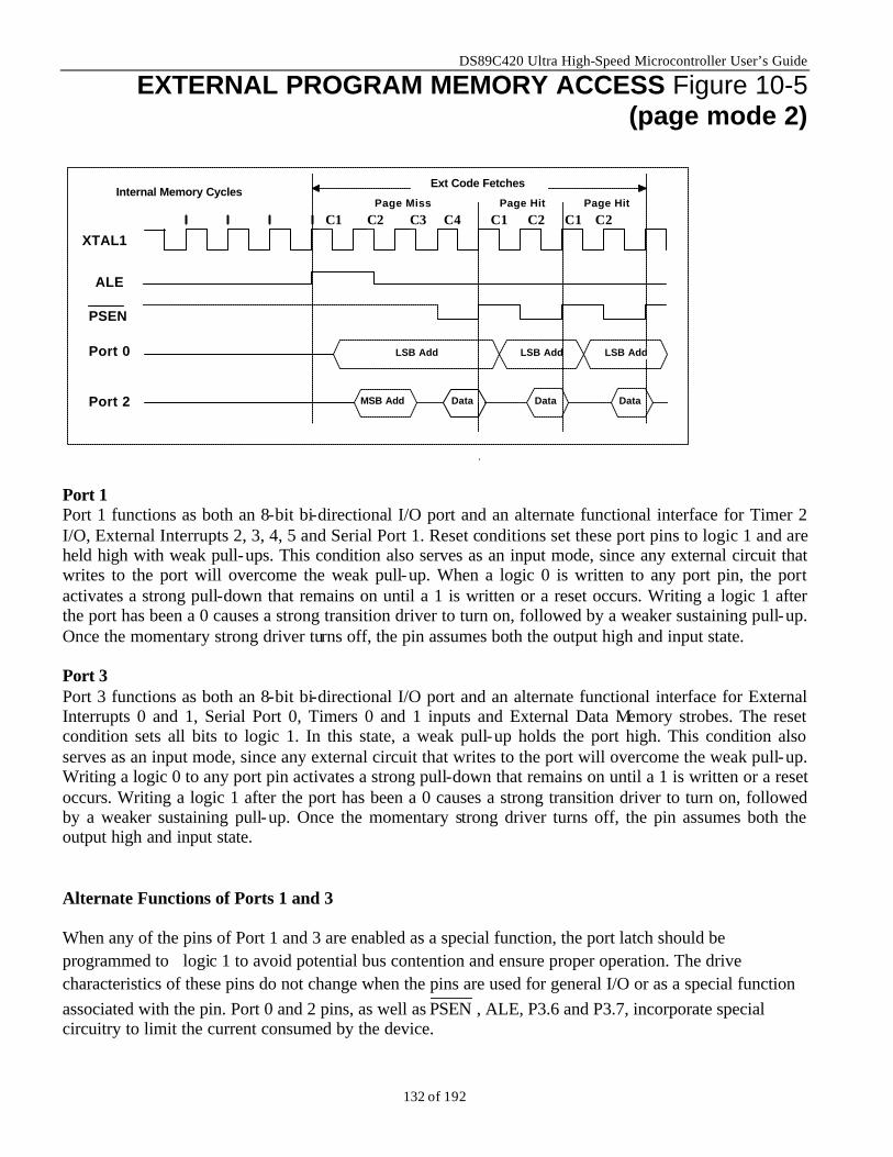
DS89C420 Ultra High-Speed Microcontroller User’s Guide
132 of 192
EXTERNAL PROGRAM MEMORY ACCESS Figure 10-5 (page mode 2)
Internal Memory Cycles
C2 C3 C4 C1 C2 C1 C2XTAL1
ALE
Port 0
Port 2
PSEN
C1
Ext Code Fetches
Page Miss Page Hit Page Hit
Data Data
LSB AddLSB Add LSB Add
DataMSB Add
Port 1 Port 1 functions as both an 8-bit bi-directional I/O port and an alternate functional interface for Timer 2 I/O, External Interrupts 2, 3, 4, 5 and Serial Port 1. Reset conditions set these port pins to logic 1 and are held high with weak pull-ups. This condition also serves as an input mode, since any external circuit that writes to the port will overcome the weak pull-up. When a logic 0 is written to any port pin, the port activates a strong pull-down that remains on until a 1 is written or a reset occurs. Writing a logic 1 after the port has been a 0 causes a strong transition driver to turn on, followed by a weaker sustaining pull-up. Once the momentary strong driver turns off, the pin assumes both the output high and input state. Port 3 Port 3 functions as both an 8-bit bi-directional I/O port and an alternate functional interface for External Interrupts 0 and 1, Serial Port 0, Timers 0 and 1 inputs and External Data Memory strobes. The reset condition sets all bits to logic 1. In this state, a weak pull-up holds the port high. This condition also serves as an input mode, since any external circuit that writes to the port will overcome the weak pull-up. Writing a logic 0 to any port pin activates a strong pull-down that remains on until a 1 is written or a reset occurs. Writing a logic 1 after the port has been a 0 causes a strong transition driver to turn on, followed by a weaker sustaining pull-up. Once the momentary strong driver turns off, the pin assumes both the output high and input state. Alternate Functions of Ports 1 and 3 When any of the pins of Port 1 and 3 are enabled as a special function, the port latch should be programmed to logic 1 to avoid potential bus contention and ensure proper operation. The drive characteristics of these pins do not change when the pins are used for general I/O or as a special function associated with the pin. Port 0 and 2 pins, as well as PSEN , ALE, P3.6 and P3.7, incorporate special circuitry to limit the current consumed by the device.
DS89C420 Ultra High-Speed Microcontroller User’s Guide
133 of 192
The special functions and the associated port pins are listed below: P1.0 T2 Timer 2 output P1.1 T2EX Timer 2 capture/reload input P1.2 RXD1 Seria l receive UART1 P1.3 TXD1 Serial transmit UART1 P1.4 INT2 External interrupt 2, rising edge active P1.5 3INT External interrupt 3, falling edge active P1.6 INT4 External interrupt 4, rising edge active P1.7 5INT External interrupt 5, falling edge active P3.0 RXD0 Serial receive UART0 P3.1 TXD0 Serial transmit UART0 P3.2 0INT External interrupt 0, falling edge active P3.3 1INT External interrupt 1, falling edge active P3.4 T0 Timer 0 input P3.5 T1 Timer 1 input P3.6 WR External data memory write strobe P3.7 RD External data memory read strobe Read-Modify-Write The normal read instructions associated with the I/O ports will read the pin state without regard to the port latches. However, the Read-Modify-Write instructions read the state of the port latches instead of the port pins. This type of instruction reads the contents of an SFR, then modifies it in the ALU and returns it to the original source. The instructions of this type are listed below: ANL Logical AND ORL Logical OR XRL Logical Exclusive OR JBC Branch if Bit Set and Clear bit CPL Complement bit INC Increment DEC Decrement DJNZ Decrement and Branch if not Zero MOV Px.n, C Move Carry bit to bit n of Port x CLR Px.n Clear bit n in Port x SETB Px.n Set bit n in Port x Output Functions The DS89C420 I/O ports appear to be true I/O, but their output characteristics are dependent on the individual port and pin conditions. When software writes logic 0 to the port for output, the port is pulled to ground. When software writes logic 1 to the port for output, Ports 1, 2 or 3 will drive weak pull-ups (after the strong transition from 0 to 1). Thus, as long as the port is not heavily loaded, true logic values will be output. Port 0, having open-drain outputs, will tri-state when written to logic 1 and hence requires external pull-ups be present when used as an output. DC drive capability is provided in the electrical specifications. Note that the DC current available from an I/O port pin is a function of the permissible voltage drop.

DS89C420 Ultra High-Speed Microcontroller User’s Guide
134 of 192
Transition current is available to help move the port pin from logic 0 to logic 1. Since the logic 0 driver is strong, no additional drive current is needed in the 1 to 0 direction. The transition current is applied when the port latch is changed from logic 0 to logic 1. Simply writing logic 1 where a 1 was already in place does not change the strength of the pull-up. This transition current is applied for two oscillator cycles. The absolute current is not guaranteed, but is approximately 2 mA at 5V. When serving as an I/O port, the drive will vary as follows: for logic 0, the port will invoke a strong pull-down, for logic 1, the port will invoke a strong pull-up for two oscillator cycles to assist with the logic transition. Then the port will revert to a weak pull-up. This weak pull-up will be maintained until the port transitions from logic 1 to logic 0. External circuits can overdrive the weak pull-up. This allows the logic 1 output state to serve as the input state as well. Substantial DC current is available in both the high and low levels. However, the power dissipation limitations make it inadvisable to heavily load multiple pins. In general, sink and source currents should not exceed 10 mA total per port (8 bits) and 25 mA total per package. Input Functions The input state of the I/O ports is the same as that of the output logic 1. That is, the pin is pulled weakly to logic 1. This logic 1 state is easily overcome by external components. Thus, after software writes a 1 to the port pin, the port is configured for input. When the port is read by software, the state of the pin will be read. The only exception is the read-modify-write instructions, discussed earlier. If the external circuit is driving logic 1, then the pin will be logic 1. If the external circuit is driving logic 0, then it will overcome the internal pull-up. Thus the pin will be the same as the driven logic state. Note that the port latch is not altered by a read operation. Therefore, if logic 0 is driven onto a port pin from an external source, then removed, the pin will revert to the weak pull-up as determined by the internal latch.
DS89C420 Ultra High-Speed Microcontroller User’s Guide
135 of 192
SECTION 11: PROGRAMMABLE TIMERS The Ultra High-Speed Microcontroller incorporates three 16-bit programmable timers and has a Watchdog Timer with a programmable interval. Because the Watchdog Timer is significantly different from the other timers, it is described separately. The 16-bit Timers are referred to simply as timers. The three timers offer the same controls and I/O functions that were available in the 80C32. As mentioned above, the actual timing of these functions is user selectable to be compatible with the instruction cycle of the older generation of 8051 family (12 clocks per tick) or the new generation (1 clock per tick). The timing for each of the three timers can be selected independently and can be changed dynamically. In most modes, the timers can be used as either counters of external events or timers. When functioning as a counter, 1 to 0 transitions on a port pin are monitored and counted. When functioning as timers, they effectively count oscillator or system clock cycles. The time base for the timer function is detailed later in this section. Because an input clock pulse must be sampled high for two system clock cycles and low for two system clock cycles in order to be recognized, this sets the maximum sampling frequency on any timer input at 1/4 of the main system clock frequency. Since the Ultra High-Speed Microcontroller timers have a variety of features, the following lists summarize the capabilities. Timer 0 Timer 1 Timer 2 13–bit Timer/counter 13–bit Timer/counter 16–bit Timer/counter 16–bit Timer/counter 16–bit Timer/counter 16–bit Timer with capture 8–bit Timer w/ Auto–reload 8–bit Timer w/ Auto–reload 16–bit Auto–reload Timer/counter Two 8–bit Timer/counters External control pulse timer/counter 16–bit up/down auto–reload External control pulse timer/counter Baud rate generator Timer/counter Baud rate generator Timer output clock generator
16-BIT TIMERS
Timers 0 and 1 are nearly identical. Timer 2 has several additional features such as up/down counting, capture values and an optional output pin that make it unique. A table is provided below summarizing the SFR bits that control operation of Timers 0, 1 and 2. Detailed bit descriptions can be found in Section 4. After the table, Timers 0 and 1 are described first, followed by a separate description for Timer 2. As mentioned above, the time base for each timer can be varied and this is also discussed in more detail below.
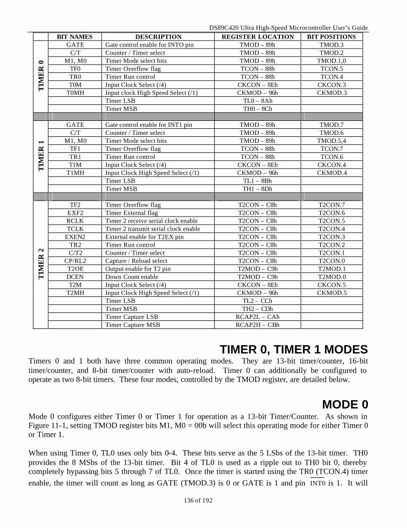
DS89C420 Ultra High-Speed Microcontroller User’s Guide
136 of 192
BIT NAMES DESCRIPTION REGISTER LOCATION BIT POSITIONS GATE Gate control enable for INTO pin TMOD – 89h TMOD.3
C/T Counter / Timer select TMOD – 89h TMOD.2 M1, M0 Timer Mode select bits TMOD – 89h TMOD.1,0
TF0 Timer Overflow flag TCON – 88h TCON.5 TR0 Timer Run control TCON – 88h TCON.4 T0M Input Clock Select (/4) CKCON – 8Eh CKCON.3
T0MH Input clock High Speed Select (/1) CKMOD – 96h CKMOD.3 Timer LSB TL0 – 8Ah
TIM
ER
0
Timer MSB TH0 – 8Ch
GATE Gate control enable for INT1 pin TMOD – 89h TMOD.7 C/T Counter / Timer select TMOD – 89h TMOD.6
M1, M0 Timer Mode select bits TMOD – 89h TMOD.5,4 TF1 Timer Overflow flag TCON – 88h TCON.7 TR1 Timer Run control TCON – 88h TCON.6 T1M Input Clock Select (/4) CKCON – 8Eh CKCON.4
T1MH Input Clock High Speed Select (/1) CKMOD – 96h CKMOD.4 Timer LSB TL1 – 8Bh
TIM
ER
1
Timer MSB TH1 – 8Dh
TF2 Timer Overflow flag T2CON – C8h T2CON.7 EXF2 Timer External flag T2CON – C8h T2CON.6 RCLK Timer 2 receive serial clock enable T2CON – C8h T2CON.5 TCLK Timer 2 transmit serial clock enable T2CON – C8h T2CON.4
EXEN2 External enable for T2EX pin T2CON – C8h T2CON.3 TR2 Timer Run control T2CON – C8h T2CON.2 C/T2 Counter / Timer select T2CON – C8h T2CON.1
CP/RL2 Capture / Reload select T2CON – C8h T2CON.0 T2OE Output enable for T2 pin T2MOD – C9h T2MOD.1 DCEN Down Count enable T2MOD – C9h T2MOD.0 T2M Input Clock Select (/4) CKCON – 8Eh CKCON.5
T2MH Input Clock High Speed Select (/1) CKMOD – 96h CKMOD.5 Timer LSB TL2 – CCh Timer MSB TH2 – CDh Timer Capture LSB RCAP2L – CAh
TIM
ER
2
Timer Capture MSB RCAP2H – CBh
TIMER 0, TIMER 1 MODES
Timers 0 and 1 both have three common operating modes. They are 13-bit timer/counter, 16-bit timer/counter, and 8-bit timer/counter with auto-reload. Timer 0 can additionally be configured to operate as two 8-bit timers. These four modes, controlled by the TMOD register, are detailed below.
MODE 0
Mode 0 configures either Timer 0 or Timer 1 for operation as a 13-bit Timer/Counter. As shown in Figure 11-1, setting TMOD register bits M1, M0 = 00b will select this operating mode for either Timer 0 or Timer 1. When using Timer 0, TL0 uses only bits 0-4. These bits serve as the 5 LSbs of the 13-bit timer. TH0 provides the 8 MSbs of the 13-bit timer. Bit 4 of TL0 is used as a ripple out to TH0 bit 0, thereby completely bypassing bits 5 through 7 of TL0. Once the timer is started using the TR0 (TCON.4) timer enable, the timer will count as long as GATE (TMOD.3) is 0 or GATE is 1 and pin INT0 is 1. It will
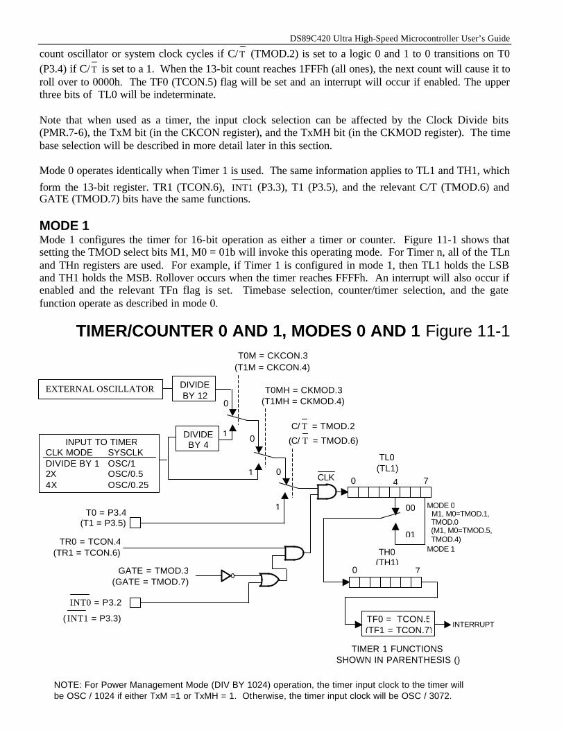
DS89C420 Ultra High-Speed Microcontroller User’s Guide
137 of 192
count oscillator or system clock cycles if C/ T (TMOD.2) is set to a logic 0 and 1 to 0 transitions on T0 (P3.4) if C/ T is set to a 1. When the 13-bit count reaches 1FFFh (all ones), the next count will cause it to roll over to 0000h. The TF0 (TCON.5) flag will be set and an interrupt will occur if enabled. The upper three bits of TL0 will be indeterminate. Note that when used as a timer, the input clock selection can be affected by the Clock Divide bits (PMR.7-6), the TxM bit (in the CKCON register), and the TxMH bit (in the CKMOD register). The time base selection will be described in more detail later in this section. Mode 0 operates identically when Timer 1 is used. The same information applies to TL1 and TH1, which form the 13-bit register. TR1 (TCON.6), INT1 (P3.3), T1 (P3.5), and the relevant C/T (TMOD.6) and GATE (TMOD.7) bits have the same functions. MODE 1 Mode 1 configures the timer for 16-bit operation as either a timer or counter. Figure 11-1 shows that setting the TMOD select bits M1, M0 = 01b will invoke this operating mode. For Timer n, all of the TLn and THn registers are used. For example, if Timer 1 is configured in mode 1, then TL1 holds the LSB and TH1 holds the MSB. Rollover occurs when the timer reaches FFFFh. An interrupt will also occur if enabled and the relevant TFn flag is set. Timebase selection, counter/timer selection, and the gate function operate as described in mode 0.
TIMER/COUNTER 0 AND 1, MODES 0 AND 1 Figure 11-1
MODE 0 M1, M0=TMOD.1, TMOD.0 (M1, M0=TMOD.5, TMOD.4) MODE 1
INPUT TO TIMER CLK MODE SYSCLK DIVIDE BY 1 OSC/1 2X OSC/0.5 4X OSC/0.25
DIVIDE BY 12
DIVIDE BY 4
T0 = P3.4(T1 = P3.5)
TR0 = TCON.4 (TR1 = TCON.6)
GATE = TMOD.3(GATE = TMOD.7)
INT0 = P3.2
( INT1 = P3.3) TF0 = TCON.5 (TF1 = TCON.7)
TIMER 1 FUNCTIONS SHOWN IN PARENTHESIS ()
INTERRUPT
TL0 (TL1)
0 4 7
00
01
0 7
TH0 (TH1)
CLK
0
1 0
1
T0M = CKCON.3 (T1M = CKCON.4)
C/ T = TMOD.2
(C/ T = TMOD.6)
0
EXTERNAL OSCILLATOR T0MH = CKMOD.3 (T1MH = CKMOD.4)
1
NOTE: For Power Management Mode (DIV BY 1024) operation, the timer input clock to the timer will be OSC / 1024 if either TxM =1 or TxMH = 1. Otherwise, the timer input clock will be OSC / 3072.
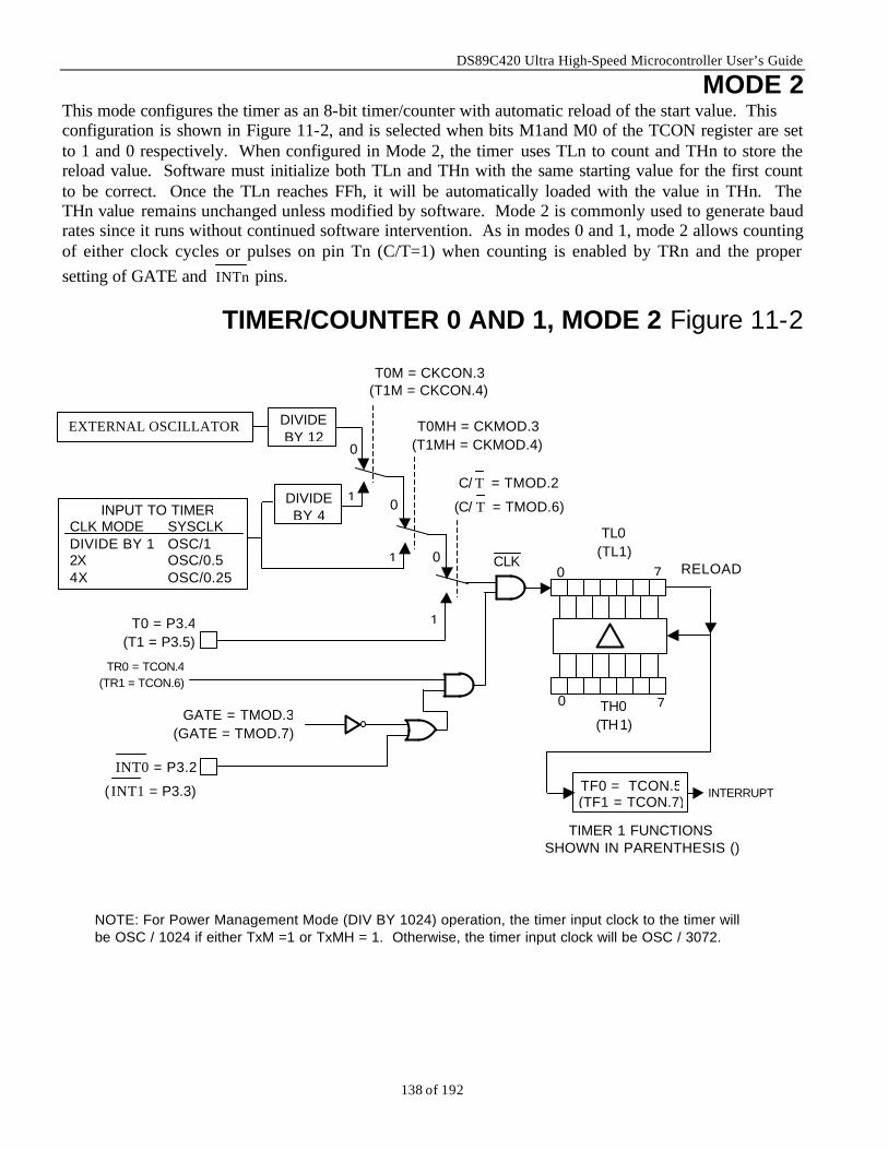
DS89C420 Ultra High-Speed Microcontroller User’s Guide
138 of 192
MODE 2 This mode configures the timer as an 8-bit timer/counter with automatic reload of the start value. This configuration is shown in Figure 11-2, and is selected when bits M1and M0 of the TCON register are set to 1 and 0 respectively. When configured in Mode 2, the timer uses TLn to count and THn to store the reload value. Software must initialize both TLn and THn with the same starting value for the first count to be correct. Once the TLn reaches FFh, it will be automatically loaded with the value in THn. The THn value remains unchanged unless modified by software. Mode 2 is commonly used to generate baud rates since it runs without continued software intervention. As in modes 0 and 1, mode 2 allows counting of either clock cycles or pulses on pin Tn (C/T=1) when counting is enabled by TRn and the proper setting of GATE and INTn pins.
TIMER/COUNTER 0 AND 1, MODE 2 Figure 11-2
T0 = P3.4(T1 = P3.5)
TR0 = TCON.4(TR1 = TCON.6)
GATE = TMOD.3(GATE = TMOD.7)
TF0 = TCON.5 (TF1 = TCON.7)
TIMER 1 FUNCTIONS SHOWN IN PARENTHESIS ()
INTERRUPT
TL0 (TL1)
0 7
0 7 TH0 (TH1)
1
RELOAD
INT0 = P3.2
( INT1 = P3.3)
CLK
INPUT TO TIMER CLK MODE SYSCLK DIVIDE BY 1 OSC/1 2X OSC/0.5 4X OSC/0.25
DIVIDE BY 12
DIVIDE BY 4
0
1 0
0
EXTERNAL OSCILLATOR
1
T0M = CKCON.3 (T1M = CKCON.4)
T0MH = CKMOD.3 (T1MH = CKMOD.4)
C/ T = TMOD.2
(C/ T = TMOD.6)
NOTE: For Power Management Mode (DIV BY 1024) operation, the timer input clock to the timer will be OSC / 1024 if either TxM =1 or TxMH = 1. Otherwise, the timer input clock will be OSC / 3072.
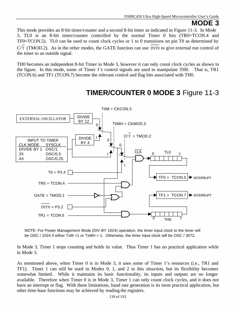
DS89C420 Ultra High-Speed Microcontroller User’s Guide
139 of 192
MODE 3 This mode provides an 8-bit timer/counter and a second 8-bit timer as indicated in Figure 11-3. In Mode 3, TL0 is an 8-bit timer/counter controlled by the normal Timer 0 bits (TR0=TCON.4 and TF0=TCON.5). TL0 can be used to count clock cycles or 1 to 0 transitions on pin T0 as determined by C/T (TMOD.2). As in the other modes, the GATE function can use INT0 to give external run control of the timer to an outside signal. TH0 becomes an independent 8-bit Timer in Mode 3, however it can only count clock cycles as shown in the figure. In this mode, some of Timer 1’s control signals are used to manipulate TH0. That is, TR1 (TCON.6) and TF1 (TCON.7) become the relevant control and flag bits associated with TH0.
TIMER/COUNTER 0 MODE 3 Figure 11-3 In Mode 3, Timer 1 stops counting and holds its value. Thus Timer 1 has no practical application while in Mode 3. As mentioned above, when Timer 0 is in Mode 3, it uses some of Timer 1’s resources (i.e., TR1 and TF1). Timer 1 can still be used in Modes 0, 1, and 2 in this situa tion, but its flexibility becomes somewhat limited. While it maintains its basic functionality, its inputs and outputs are no longer available. Therefore when Timer 0 is in Mode 3, Timer 1 can only count clock cycles, and it does not have an interrupt or flag. With these limitations, baud rate generation is its most practical application, but other time-base functions may be achieved by reading the registers.
T0 = P3.4
TR0 = TCON.4
GATE = TMOD.3
TL0 0 7
0 7 TH0
0
1
TR1 = TCON.6
TF0 = TCON.5 INTERRUPT
TF1 = TCON.7
C/ T = TMOD.2
INT0 = P3.2
CLK
INTERRUPT
INPUT TO TIMER CLK MODE SYSCLK DIVIDE BY 1 OSC/1 2X OSC/0.5 4X OSC/0.25
DIVIDE BY 12
DIVIDE BY 4
0
1
0
EXTERNAL OSCILLATOR
1
T0M = CKCON.3
T0MH = CKMOD.3
NOTE: For Power Management Mode (DIV BY 1024) operation, the timer input clock to the timer will be OSC / 1024 if either TxM =1 or TxMH = 1. Otherwise, the timer input clock will be OSC / 3072.
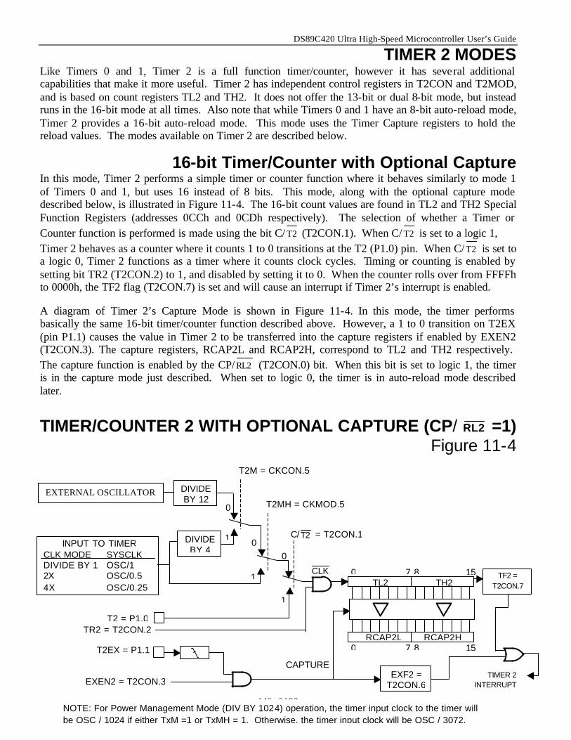
DS89C420 Ultra High-Speed Microcontroller User’s Guide
140 of 192
TIMER 2 MODES Like Timers 0 and 1, Timer 2 is a full function timer/counter, however it has several additional capabilities that make it more useful. Timer 2 has independent control registers in T2CON and T2MOD, and is based on count registers TL2 and TH2. It does not offer the 13-bit or dual 8-bit mode, but instead runs in the 16-bit mode at all times. Also note that while Timers 0 and 1 have an 8-bit auto-reload mode, Timer 2 provides a 16-bit auto-reload mode. This mode uses the Timer Capture registers to hold the reload values. The modes available on Timer 2 are described below.
16-bit Timer/Counter with Optional Capture In this mode, Timer 2 performs a simple timer or counter function where it behaves similarly to mode 1 of Timers 0 and 1, but uses 16 instead of 8 bits. This mode, along with the optional capture mode described below, is illustrated in Figure 11-4. The 16-bit count values are found in TL2 and TH2 Special Function Registers (addresses 0CCh and 0CDh respectively). The selection of whether a Timer or Counter function is performed is made using the bit C/ T2 (T2CON.1). When C/ T2 is set to a logic 1, Timer 2 behaves as a counter where it counts 1 to 0 transitions at the T2 (P1.0) pin. When C/ T2 is set to a logic 0, Timer 2 functions as a timer where it counts clock cycles. Timing or counting is enabled by setting bit TR2 (T2CON.2) to 1, and disabled by setting it to 0. When the counter rolls over from FFFFh to 0000h, the TF2 flag (T2CON.7) is set and will cause an interrupt if Timer 2’s interrupt is enabled. A diagram of Timer 2’s Capture Mode is shown in Figure 11-4. In this mode, the timer performs basically the same 16-bit timer/counter function described above. However, a 1 to 0 transition on T2EX (pin P1.1) causes the value in Timer 2 to be transferred into the capture registers if enabled by EXEN2 (T2CON.3). The capture registers, RCAP2L and RCAP2H, correspond to TL2 and TH2 respectively. The capture function is enabled by the CP/ RL2 (T2CON.0) bit. When this bit is set to logic 1, the timer is in the capture mode just described. When set to logic 0, the timer is in auto-reload mode described later.
TIMER/COUNTER 2 WITH OPTIONAL CAPTURE (CP/ RL2 =1)
Figure 11-4
NOTE: For Power Management Mode (DIV BY 1024) operation, the timer input clock to the timer will be OSC / 1024 if either TxM =1 or TxMH = 1. Otherwise, the timer input clock will be OSC / 3072.
T2 = P1.0TR2 = T2CON.2
EXEN2 = T2CON.3 EXF2 =
T2CON.6
CAPTURE TIMER 2
INTERRUPT
0
1
TL2 0 7
TH2 8 15 TF2 =
T2CON.7
0 7 8 15 RCAP2L RCAP2H
T2EX = P1.1
C/T2 = T2CON.1
CLK
INPUT TO TIMER CLK MODE SYSCLK DIVIDE BY 1 OSC/1 2X OSC/0.5 4X OSC/0.25
DIVIDE BY 12
DIVIDE BY 4
0
1
0
EXTERNAL OSCILLATOR
1
T2M = CKCON.5
T2MH = CKMOD.5
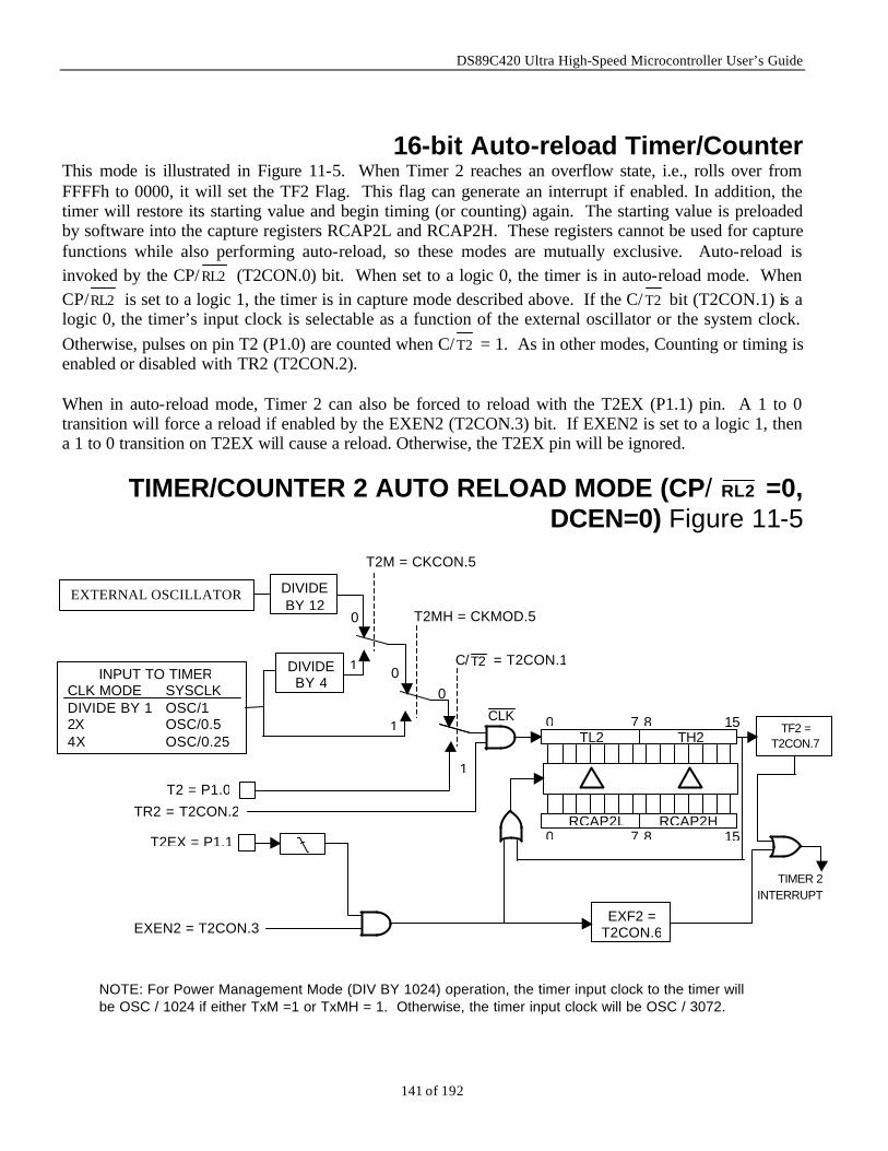
DS89C420 Ultra High-Speed Microcontroller User’s Guide
141 of 192
16-bit Auto-reload Timer/Counter This mode is illustrated in Figure 11-5. When Timer 2 reaches an overflow state, i.e., rolls over from FFFFh to 0000, it will set the TF2 Flag. This flag can generate an interrupt if enabled. In addition, the timer will restore its starting value and begin timing (or counting) again. The starting value is preloaded by software into the capture registers RCAP2L and RCAP2H. These registers cannot be used for capture functions while also performing auto-reload, so these modes are mutually exclusive. Auto-reload is invoked by the CP/ RL2 (T2CON.0) bit. When set to a logic 0, the timer is in auto-reload mode. When CP/RL2 is set to a logic 1, the timer is in capture mode described above. If the C/ T2 bit (T2CON.1) is a logic 0, the timer’s input clock is selectable as a function of the external oscillator or the system clock. Otherwise, pulses on pin T2 (P1.0) are counted when C/ T2 = 1. As in other modes, Counting or timing is enabled or disabled with TR2 (T2CON.2). When in auto-reload mode, Timer 2 can also be forced to reload with the T2EX (P1.1) pin. A 1 to 0 transition will force a reload if enabled by the EXEN2 (T2CON.3) bit. If EXEN2 is set to a logic 1, then a 1 to 0 transition on T2EX will cause a reload. Otherwise, the T2EX pin will be ignored.
TIMER/COUNTER 2 AUTO RELOAD MODE (CP/ RL2 =0, DCEN=0) Figure 11-5
T2 = P1.0
TR2 = T2CON.2
EXEN2 = T2CON.3EXF2 =
T2CON.6
TIMER 2 INTERRUPT
1
T2M = CKCON.5
TL2 0 7
TH2 8 15 TF2 =
T2CON.7
0 7 8 15 RCAP2L RCAP2H
T2EX = P1.1
0 INPUT TO TIMER CLK MODE SYSCLK DIVIDE BY 1 OSC/1 2X OSC/0.5 4X OSC/0.25
DIVIDE BY 12
DIVIDE BY 4
0
1
0
EXTERNAL OSCILLATOR
1
T2MH = CKMOD.5
C/T2 = T2CON.1
CLK
NOTE: For Power Management Mode (DIV BY 1024) operation, the timer input clock to the timer will be OSC / 1024 if either TxM =1 or TxMH = 1. Otherwise, the timer input clock will be OSC / 3072.
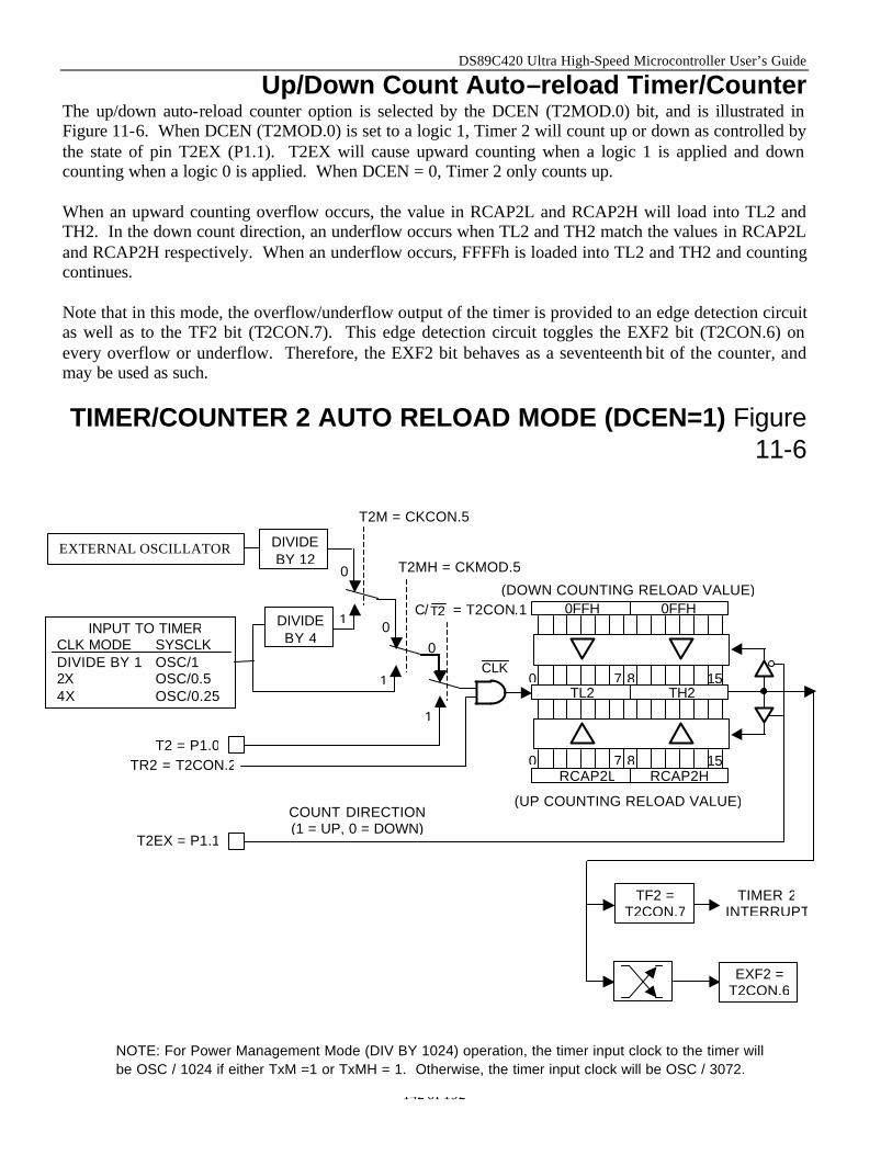
DS89C420 Ultra High-Speed Microcontroller User’s Guide
142 of 192
Up/Down Count Auto–reload Timer/Counter The up/down auto-reload counter option is selected by the DCEN (T2MOD.0) bit, and is illustrated in Figure 11-6. When DCEN (T2MOD.0) is set to a logic 1, Timer 2 will count up or down as controlled by the state of pin T2EX (P1.1). T2EX will cause upward counting when a logic 1 is applied and down counting when a logic 0 is applied. When DCEN = 0, Timer 2 only counts up. When an upward counting overflow occurs, the value in RCAP2L and RCAP2H will load into TL2 and TH2. In the down count direction, an underflow occurs when TL2 and TH2 match the values in RCAP2L and RCAP2H respectively. When an underflow occurs, FFFFh is loaded into TL2 and TH2 and counting continues. Note that in this mode, the overflow/underflow output of the timer is provided to an edge detection circuit as well as to the TF2 bit (T2CON.7). This edge detection circuit toggles the EXF2 bit (T2CON.6) on every overflow or underflow. Therefore, the EXF2 bit behaves as a seventeenth bit of the counter, and may be used as such.
TIMER/COUNTER 2 AUTO RELOAD MODE (DCEN=1) Figure 11-6
T2 = P1.0TR2 = T2CON.2
1
T2M = CKCON.5
RCAP2L RCAP2H
0FFH 0FFH
0 7 8 15 TL2 TH2
(DOWN COUNTING RELOAD VALUE)
0 7 8 15
T2EX = P1.1
(UP COUNTING RELOAD VALUE)
TF2 = T2CON.7
TIMER 2 INTERRUPT
EXF2 = T2CON.6
COUNT DIRECTION (1 = UP, 0 = DOWN)
C/T2 = T2CON.1
CLK
0 INPUT TO TIMER CLK MODE SYSCLK DIVIDE BY 1 OSC/1 2X OSC/0.5 4X OSC/0.25
DIVIDE BY 12
DIVIDE BY 4
0
1
0
EXTERNAL OSCILLATOR
1
T2MH = CKMOD.5
NOTE: For Power Management Mode (DIV BY 1024) operation, the timer input clock to the timer will be OSC / 1024 if either TxM =1 or TxMH = 1. Otherwise, the timer input clock will be OSC / 3072.

DS89C420 Ultra High-Speed Microcontroller User’s Guide
143 of 192
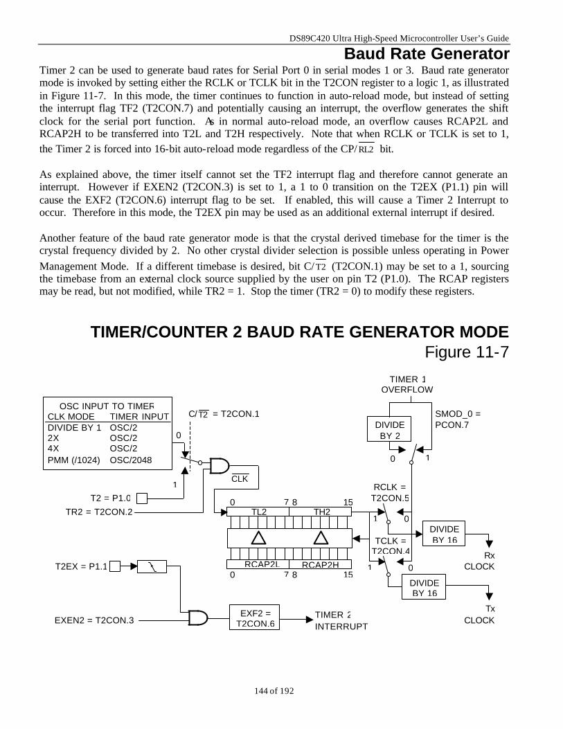
DS89C420 Ultra High-Speed Microcontroller User’s Guide
144 of 192
Baud Rate Generator Timer 2 can be used to generate baud rates for Serial Port 0 in serial modes 1 or 3. Baud rate generator mode is invoked by setting either the RCLK or TCLK bit in the T2CON register to a logic 1, as illustrated in Figure 11-7. In this mode, the timer continues to function in auto-reload mode, but instead of setting the interrupt flag TF2 (T2CON.7) and potentially causing an interrupt, the overflow generates the shift clock for the serial port function. As in normal auto-reload mode, an overflow causes RCAP2L and RCAP2H to be transferred into T2L and T2H respectively. Note that when RCLK or TCLK is set to 1, the Timer 2 is forced into 16-bit auto-reload mode regardless of the CP/ RL2 bit. As explained above, the timer itself cannot set the TF2 interrupt flag and therefore cannot generate an interrupt. However if EXEN2 (T2CON.3) is set to 1, a 1 to 0 transition on the T2EX (P1.1) pin will cause the EXF2 (T2CON.6) interrupt flag to be set. If enabled, this will cause a Timer 2 Interrupt to occur. Therefore in this mode, the T2EX pin may be used as an additional external interrupt if desired. Another feature of the baud rate generator mode is that the crystal derived timebase for the timer is the crystal frequency divided by 2. No other crystal divider selection is possible unless operating in Power Management Mode. If a different timebase is desired, bit C/ T2 (T2CON.1) may be set to a 1, sourcing the timebase from an external clock source supplied by the user on pin T2 (P1.0). The RCAP registers may be read, but not modified, while TR2 = 1. Stop the timer (TR2 = 0) to modify these registers.
TIMER/COUNTER 2 BAUD RATE GENERATOR MODE Figure 11-7
OSC INPUT TO TIMER CLK MODE TIMER INPUT DIVIDE BY 1 OSC/2 2X OSC/2 4X OSC/2 PMM (/1024) OSC/2048
DIVIDE BY 2
T2 = P1.0
TR2 = T2CON.2
EXEN2 = T2CON.3 EXF2 =
T2CON.6 TIMER 2 INTERRUPT
0
1
TL2 0 7
TH2 8 15
RCLK = T2CON.5
0 7 8 15 RCAP2L RCAP2H T2EX = P1.1
TxCLOCK
DIVIDE BY 16
RxCLOCK
DIVIDE BY 16
SMOD_0 = PCON.7
TCLK = T2CON.4
1 0
1 0
0 1
TIMER 1 OVERFLOW
C/T2 = T2CON.1
CLK
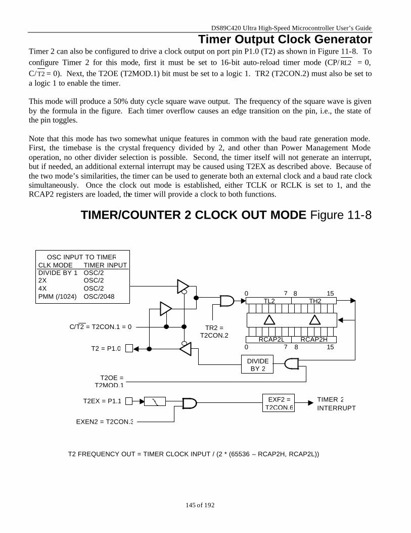
DS89C420 Ultra High-Speed Microcontroller User’s Guide
145 of 192
Timer Output Clock Generator Timer 2 can also be configured to drive a clock output on port pin P1.0 (T2) as shown in Figure 11-8. To configure Timer 2 for this mode, first it must be set to 16-bit auto-reload timer mode (CP/ RL2 = 0, C/T2 = 0). Next, the T2OE (T2MOD.1) bit must be set to a logic 1. TR2 (T2CON.2) must also be set to a logic 1 to enable the timer. This mode will produce a 50% duty cycle square wave output. The frequency of the square wave is given by the formula in the figure. Each timer overflow causes an edge transition on the pin, i.e., the state of the pin toggles. Note that this mode has two somewhat unique features in common with the baud rate generation mode. First, the timebase is the crystal frequency divided by 2, and other than Power Management Mode operation, no other divider selection is possible. Second, the timer itself will not generate an interrupt, but if needed, an additional external interrupt may be caused using T2EX as described above. Because of the two mode’s similarities, the timer can be used to generate both an external clock and a baud rate clock simultaneously. Once the clock out mode is established, either TCLK or RCLK is set to 1, and the RCAP2 registers are loaded, the timer will provide a clock to both functions.
TIMER/COUNTER 2 CLOCK OUT MODE Figure 11-8
EXF2 = T2CON.6
DIVIDE BY 2
T2EX = P1.1
EXEN2 = T2CON.3
RCAP2L RCAP2H
0 15 TL2 TH2
0 7 8 15 T2 = P1.0
7 8
C/T2 = T2CON.1 = 0 TR2 = T2CON.2
T2OE = T2MOD.1
TIMER 2 INTERRUPT
OSC INPUT TO TIMER CLK MODE TIMER INPUT DIVIDE BY 1 OSC/2 2X OSC/2 4X OSC/2 PMM (/1024) OSC/2048
T2 FREQUENCY OUT = TIMER CLOCK INPUT / (2 * (65536 – RCAP2H, RCAP2L))
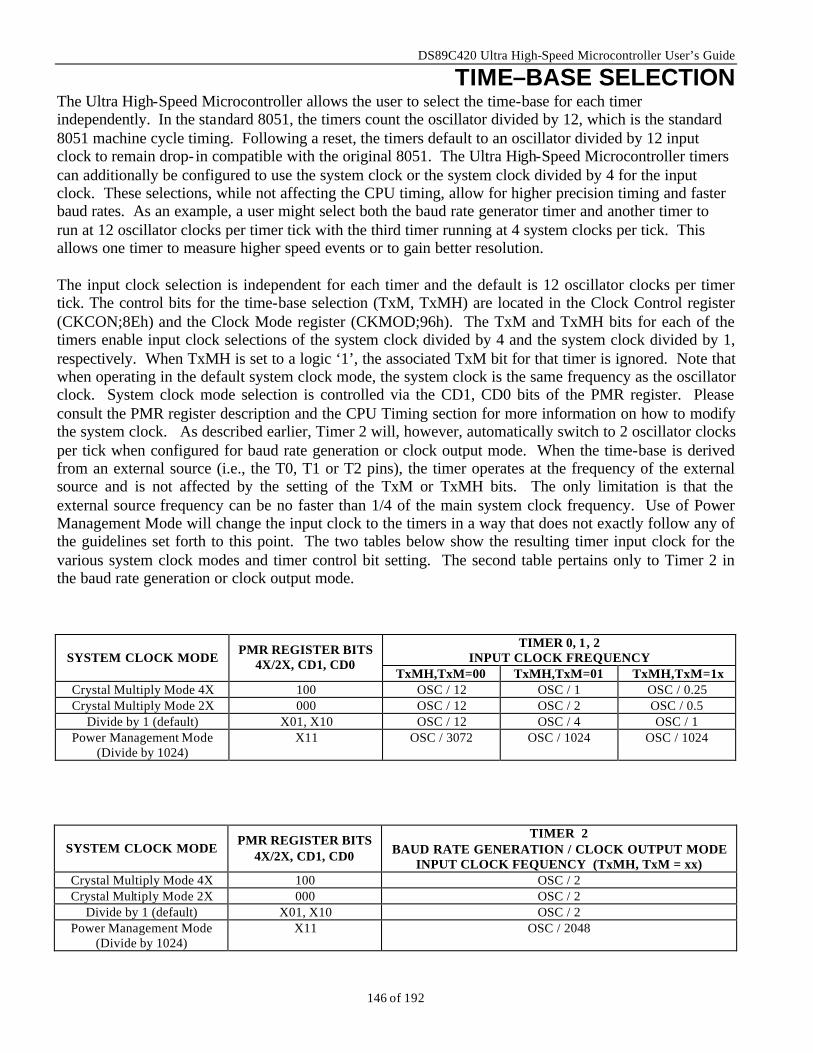
DS89C420 Ultra High-Speed Microcontroller User’s Guide
146 of 192
TIME–BASE SELECTION The Ultra High-Speed Microcontroller allows the user to select the time-base for each timer independently. In the standard 8051, the timers count the oscillator divided by 12, which is the standard 8051 machine cycle timing. Following a reset, the timers default to an oscillator divided by 12 input clock to remain drop- in compatible with the original 8051. The Ultra High-Speed Microcontroller timers can additionally be configured to use the system clock or the system clock divided by 4 for the input clock. These selections, while not affecting the CPU timing, allow for higher precision timing and faster baud rates. As an example, a user might select both the baud rate generator timer and another timer to run at 12 oscillator clocks per timer tick with the third timer running at 4 system clocks per tick. This allows one timer to measure higher speed events or to gain better resolution. The input clock selection is independent for each timer and the default is 12 oscillator clocks per timer tick. The control bits for the time-base selection (TxM, TxMH) are located in the Clock Control register (CKCON;8Eh) and the Clock Mode register (CKMOD;96h). The TxM and TxMH bits for each of the timers enable input clock selections of the system clock divided by 4 and the system clock divided by 1, respectively. When TxMH is set to a logic ‘1’, the associated TxM bit for that timer is ignored. Note that when operating in the default system clock mode, the system clock is the same frequency as the oscillator clock. System clock mode selection is controlled via the CD1, CD0 bits of the PMR register. Please consult the PMR register description and the CPU Timing section for more information on how to modify the system clock. As described earlier, Timer 2 will, however, automatically switch to 2 oscillator clocks per tick when configured for baud rate generation or clock output mode. When the time-base is derived from an external source (i.e., the T0, T1 or T2 pins), the timer operates at the frequency of the external source and is not affected by the setting of the TxM or TxMH bits. The only limitation is that the external source frequency can be no faster than 1/4 of the main system clock frequency. Use of Power Management Mode will change the input clock to the timers in a way that does not exactly follow any of the guidelines set forth to this point. The two tables below show the resulting timer input clock for the various system clock modes and timer control bit setting. The second table pertains only to Timer 2 in the baud rate generation or clock output mode.
TIMER 0, 1, 2
INPUT CLOCK FREQUENCY SYSTEM CLOCK MODE PMR REGISTER BITS
4X/2X, CD1, CD0 TxMH,TxM=00 TxMH,TxM=01 TxMH,TxM=1x
Crystal Multiply Mode 4X 100 OSC / 12 OSC / 1 OSC / 0.25 Crystal Multiply Mode 2X 000 OSC / 12 OSC / 2 OSC / 0.5
Divide by 1 (default) X01, X10 OSC / 12 OSC / 4 OSC / 1 Power Management Mode
(Divide by 1024) X11 OSC / 3072 OSC / 1024 OSC / 1024
SYSTEM CLOCK MODE
PMR REGISTER BITS 4X/2X, CD1, CD0
TIMER 2 BAUD RATE GENERATION / CLOCK OUTPUT MODE
INPUT CLOCK FEQUENCY (TxMH, TxM = xx) Crystal Multiply Mode 4X 100 OSC / 2 Crystal Multiply Mode 2X 000 OSC / 2
Divide by 1 (default) X01, X10 OSC / 2 Power Management Mode
(Divide by 1024) X11 OSC / 2048
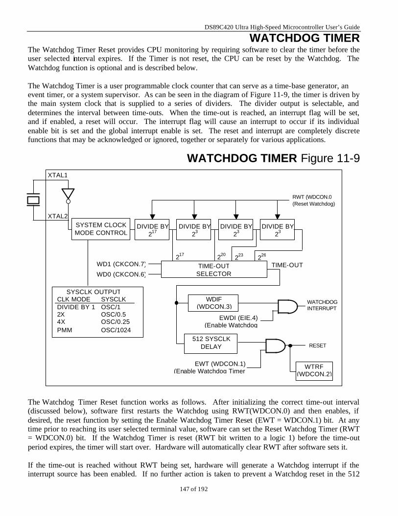
DS89C420 Ultra High-Speed Microcontroller User’s Guide
147 of 192
WATCHDOG TIMER The Watchdog Timer Reset provides CPU monitoring by requiring software to clear the timer before the user selected interval expires. If the Timer is not reset, the CPU can be reset by the Watchdog. The Watchdog function is optional and is described below. The Watchdog Timer is a user programmable clock counter that can serve as a time-base generator, an event timer, or a system supervisor. As can be seen in the diagram of Figure 11-9, the timer is driven by the main system clock that is supplied to a series of dividers. The divider output is selectable, and determines the interval between time-outs. When the time-out is reached, an interrupt flag will be set, and if enabled, a reset will occur. The interrupt flag will cause an interrupt to occur if its individual enable bit is set and the global interrupt enable is set. The reset and interrupt are completely discrete functions that may be acknowledged or ignored, together or separately for various applications.
WATCHDOG TIMER Figure 11-9 The Watchdog Timer Reset function works as follows. After initializing the correct time-out interval (discussed below), software first restarts the Watchdog using RWT(WDCON.0) and then enables, if desired, the reset function by setting the Enable Watchdog Timer Reset (EWT = WDCON.1) bit. At any time prior to reaching its user selected terminal value, software can set the Reset Watchdog Timer (RWT = WDCON.0) bit. If the Watchdog Timer is reset (RWT bit written to a logic 1) before the time-out period expires, the timer will start over. Hardware will automatically clear RWT after software sets it. If the time-out is reached without RWT being set, hardware will generate a Watchdog interrupt if the interrupt source has been enabled. If no further action is taken to prevent a Watchdog reset in the 512
DIVIDE BY 217
DIVIDE BY 23
DIVIDE BY 23
DIVIDE BY 23
RWT (WDCON.0 (Reset Watchdog)
WD1 (CKCON.7)
WD0 (CKCON.6)TIME-OUT
XTAL1
XTAL2 SYSTEM CLOCK MODE CONTROL
TIME-OUT SELECTOR
WDIF (WDCON.3)
EWDI (EIE.4)(Enable Watchdog
WATCHDOG INTERRUPT
RESET
WTRF (WDCON.2)
512 SYSCLK DELAY
EWT (WDCON.1)(Enable Watchdog Timer
217 220 223 226
SYSCLK OUTPUT CLK MODE SYSCLK DIVIDE BY 1 OSC/1 2X OSC/0.5 4X OSC/0.25 PMM OSC/1024
DS89C420 Ultra High-Speed Microcontroller User’s Guide
148 of 192
system clock cycles following the time-out, hardware has the ability to reset the CPU if EWT=1. When the reset occurs, the Watchdog Timer Reset Flag (WTRF = WDCON.2) will automatically be set to indicate the cause of the reset, however software must clear this bit manually. The Watchdog Timer is a free running timer. When used as a simple timer with both the reset and interrupt functions disabled (EWT = 0 and EWDI = 0), the timer will continue to set the Watchdog Interrupt flag each time the timer completes the selected timer interval as programmed by WD1 (CKCON.7) and WD0 (CKCON.6). Restarting the timer using the RWT (WDCON.0) bit, allows software to use the timer in a polled time-out mode. The WDIF bit is cleared by software or any reset. The Watchdog Interrupt is also available for applications that do not need a true Watchdog Reset but simply a very long timer. The interrupt is enabled using the Enable Watchdog Timer Interrupt (EWDI = EIE.4) bit. When the time-out occurs, the Watchdog Timer will set the WDIF bit (WDCON.3), and an interrupt will occur if the global interrupt enable (EA = IE.7) is set. Note that WDIF is set 512 clocks before a potential Watchdog Reset. The Watchdog Interrupt Flag will indicate the source of the interrupt, and must be cleared by software. Using the Watchdog Interrupt during software development can allow the user to select ideal watchdog reset locations. Code is first developed without enabling the Watchdog Interrupt or Reset functions. Once the program is complete, the Watchdog Interrupt function is enabled to identify the required locations in code to set the RWT (WDCON.0) bit. Incrementally adding instructions to reset the Watchdog Timer prior to each address location (identified by the Watchdog Interrupt) will allow the code to eventually run without receiving a Watchdog Interrupt. At this point the Watchdog Timer Reset can be enabled without the potential of generating unwanted resets. At the same time the Watchdog Interrupt may also be disabled. Proper use of the Watchdog Interrupt with the Watchdog Reset allows interrupt software to survey the system for errant conditions. When using the Watchdog Timer as a system monitor, the Watchdog Reset function should be used. If the Interrupt function were used, the purpose of the watchdog would be defeated. For example, assume the system is executing errant code prior to the Watchdog Interrupt. The interrupt would temporarily force the system back into control by vectoring the CPU to the interrupt service routine. Restarting the Watchdog and exiting by an RETI or RET, would return the processor to the lost position prior to the interrupt. By using the Watchdog Reset function, the processor is restarted from the beginning of the program, and therefore placed into a known state. The Watchdog time-out selection is made using bits WD1 (CKCON.7) and WD0 (CKCON.6). The Watchdog has four time-out selections based on the system clock frequency as shown in the figure. Since the time-out is a function of the system clock, the actual time-out interval is dependent on both the crystal frequency and the system clock mode. Shown below is a summary of the selectable Watchdog time-out intervals for the various system clock modes and WD1:0 control bit settings. The Watchdog Reset, if enabled, is always scheduled to occur 512 system clocks following the time-out. Watchdog generated resets will last for 13 oscillator cycles.
WATCHDOG TIME-OUT
(IN NUMBER OF OSCILLATOR CLOCKS) SYSTEM CLOCK MODE PMR REGISTER BITS
4X/2X, CD1, CD0 WD1:0=00b WD1:0=01b WD1:0=10b WD1:0=11b
Crystal Multiply Mode 4X 100 215 218 221 224
Crystal Multiply Mode 2X 000 216 219 222 225
Divide by 1 (default) X01, X10 217 220 223 226 Power Management Mode X11 227 230 233 236
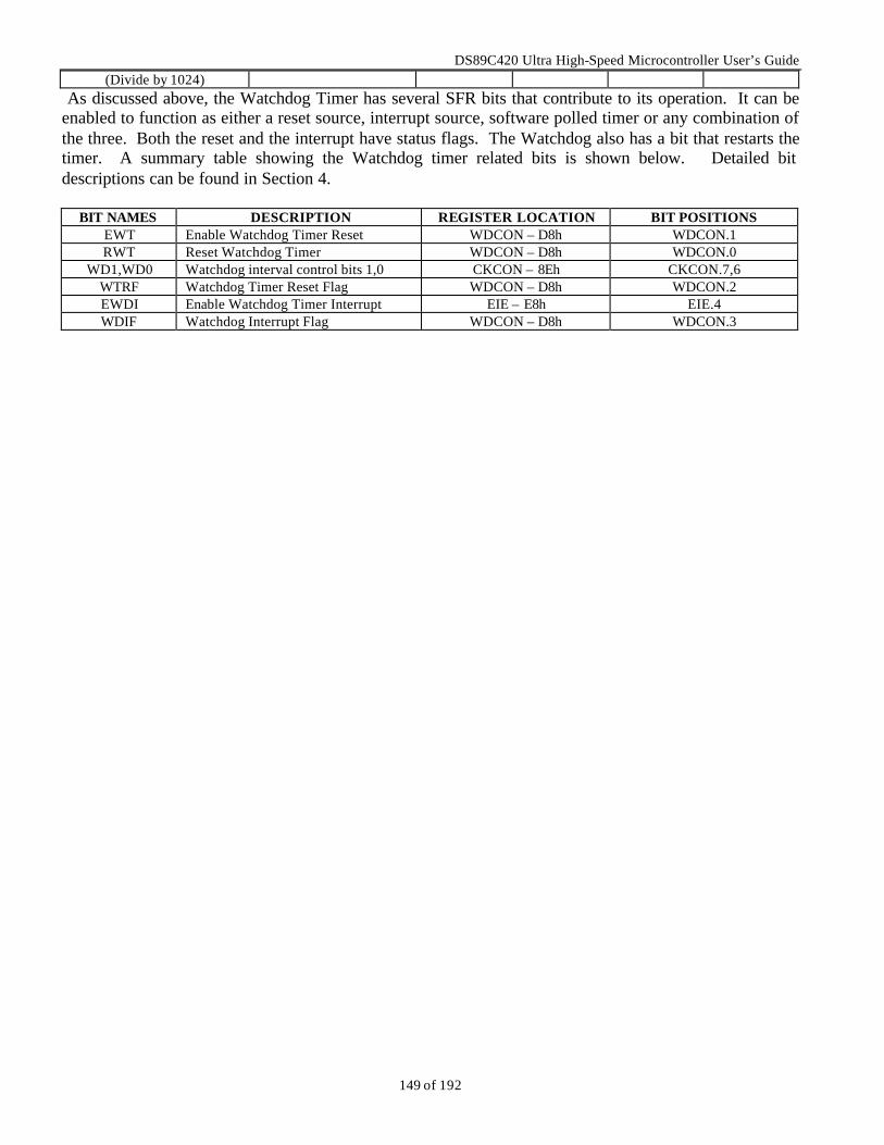
DS89C420 Ultra High-Speed Microcontroller User’s Guide
149 of 192
(Divide by 1024) As discussed above, the Watchdog Timer has several SFR bits that contribute to its operation. It can be enabled to function as either a reset source, interrupt source, software polled timer or any combination of the three. Both the reset and the interrupt have status flags. The Watchdog also has a bit that restarts the timer. A summary table showing the Watchdog timer related bits is shown below. Detailed bit descriptions can be found in Section 4.
BIT NAMES DESCRIPTION REGISTER LOCATION BIT POSITIONS EWT Enable Watchdog Timer Reset WDCON – D8h WDCON.1 RWT Reset Watchdog Timer WDCON – D8h WDCON.0
WD1,WD0 Watchdog interval control bits 1,0 CKCON – 8Eh CKCON.7,6 WTRF Watchdog Timer Reset Flag WDCON – D8h WDCON.2 EWDI Enable Watchdog Timer Interrupt EIE – E8h EIE.4 WDIF Watchdog Interrupt Flag WDCON – D8h WDCON.3
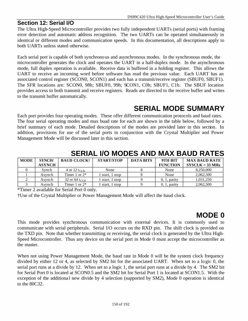
DS89C420 Ultra High-Speed Microcontroller User’s Guide
150 of 192
Section 12: Serial I/O The Ultra High-Speed Microcontroller provides two fully independent UARTs (serial ports) with framing error detection and automatic address recognition. The two UARTs can be operated simultaneously in identical or different modes and communication speeds. In this documentation, all descriptions apply to both UARTs unless stated otherwise. Each serial port is capable of both synchronous and asynchronous modes. In the synchronous mode, the microcontroller generates the clock and operates the UART in a half-duplex mode. In the asynchronous mode, full duplex operation is available. Receive data is buffered in a holding register. This allows the UART to receive an incoming word before software has read the previous value. Each UART has an associated control register (SCON0, SCON1) and each has a transmit/receive register (SBUF0, SBUF1). The SFR locations are: SCON0, 98h; SBUF0, 99h; SCON1, C0h; SBUF1, C1h. The SBUF location provides access to both transmit and receive registers. Reads are directed to the receive buffer and writes to the transmit buffer automatically.
SERIAL MODE SUMMARY Each port provides four operating modes. These offer different communication protocols and baud rates. The four serial operating modes and max buad rate for each are shown in the table below, followed by a brief summary of each mode. Detailed descriptions of the modes are provided later in this section. In addition, provisions for use of the serial ports in conjunction with the Crystal Multiplier and Power Management Mode will be discussed later in this section.
SERIAL I/O MODES AND MAX BAUD RATES
MODE SYNCH/ ASYNCH
BAUD CLOCK† START/STOP DATA BITS 9TH BIT FUNCTION
MAX BAUD RATE SYSCLK = 33 MHz
0 Synch 4 or 12 tCLK None 8 None 8,250,000 1 Asynch Timer 1 or 2* 1 start, 1 stop 8 None 2,062,500 2 Asynch 32 or 64 tCLK 1 start, 1 stop 9 0, 1, parity 1,031,250 3 Asynch Timer 1 or 2* 1 start, 1 stop 9 0, 1, parity 2,062,500
*Timer 2 available for Serial Port 0 only.
†Use of the Crystal Multiplier or Power Management Mode will affect the baud clock.
MODE 0
This mode provides synchronous communication with external devices. It is commonly used to communicate with serial peripherals. Serial I/O occurs on the RXD pin. The shift clock is provided on the TXD pin. Note that whether transmitting or receiving, the serial clock is generated by the Ultra High-Speed Microcontroller. Thus any device on the serial port in Mode 0 must accept the microcontroller as the master. When not using Power Management Mode, the baud rate in Mode 0 will be the system clock frequency divided by either 12 or 4, as selected by SM2 bit for the associated UART. When set to a lo gic 0, the serial port runs at a divide by 12. When set to a logic 1, the serial port runs at a divide by 4. The SM2 bit for Serial Port 0 is located at SCON0.5 and the SM2 bit for Serial Port 1 is located at SCON1.5. With the exception of the additiona l new divide by 4 selection (supported by SM2), Mode 0 operation is identical to the 80C32.
DS89C420 Ultra High-Speed Microcontroller User’s Guide
151 of 192
MODE 1 This mode provides standard full duplex asynchronous communication. A total of 10 bits is transmitted including 1 start bit, 8 data bits, and 1 stop bit. The received stop bit is stored in bit location RB8 of the relevant SCON register. In Mode 1, the baud rate is a function of timer overflow. This makes the baud rate programmable by the user. One difference that exists between the two UARTs, with respect to Mode 1 configuration, is that Serial Port 1 can use only Timer 1, whereas Serial Port 0 can use either Timer 1 or 2 to generate baud rates. If both serial ports use the same timer, they will be running at the same baud rate or one can run twice as fast as the other (when baud rate doubler bits, PCON.7 and WDCON.7, are configured differently). If the two UARTs use different timers, the baud rate configurations, in relation to one another, are not as restrictive. Baud rates are discussed in more detail below. Mode 1 operation is identical to the standard 80C32 when Timers 1 or 2 use the default ‘oscillator divide by 12’ as an input clock.
MODE 2 This mode is an asynchronous mode that transmits a total of 11 bits. These include 1 start bit, 9 data bits (the ninth data bit being programmable), and 1 stop bit. The ninth bit is determined by the value in TB8 (SCON0.3 or SCON1.3) for transmission. When the ninth bit is received, it is stored in RB8 (SCON0.2 or SCON1.2). The ninth bit can be a parity value by moving the P bit (PSW.0) to TB8. When not using the Power Management Mode, the baud rate for Mode 2 is a function only of the oscillator frequency. It is either the oscillator input divided by 32 or 64 as programmed by the SMOD doubler bit for the associated UART. The SMOD_0 baud rate doubler bit for Serial Port 0 is located at PCON.7 and the SMOD_1 baud rate doubler bit for Serial Port 1 is located at WDCON.7. Mode 2 operation is identical to the standard 80C32.
MODE 3 This mode has the same functionality as Mode 2, but generates baud rates like Mode 1. That is, this mode transmits 11 bits, but generates baud rates via the timers. Like Mode 1, either Timer 1 or 2 can be used for Serial Port 0 and Timer 1 can be used for Serial Port 1. Mode 3 operation is identical to the standard 80C32 when Timers 1 or 2 use the default ‘oscillator divide by 12’ as an input clock.
SERIAL PORT INITIALIZATION In order to use the UART function(s), the serial port must be initialized. This involves selecting the mode and time base, then initializing the baud rate generator if necessary. Serial communication is then available. Once the baud rate generator is running, the UART can receive data. In Mode 0, the High-Speed Microcontroller provides the clock. Serial reception is initiated by setting the RI bit to a logic 0 and REN to a logic 1. This will generate a clock on the TXD pin and shift in the 8 bits on the RXD pin. In the other modes, setting the REN bit to a logic 1 will allow serial reception, but the external device must actually initiate it by sending a start bit. In any mode, serial transmission is initiated by writing to either the SBUF0 or SBUF1 location.
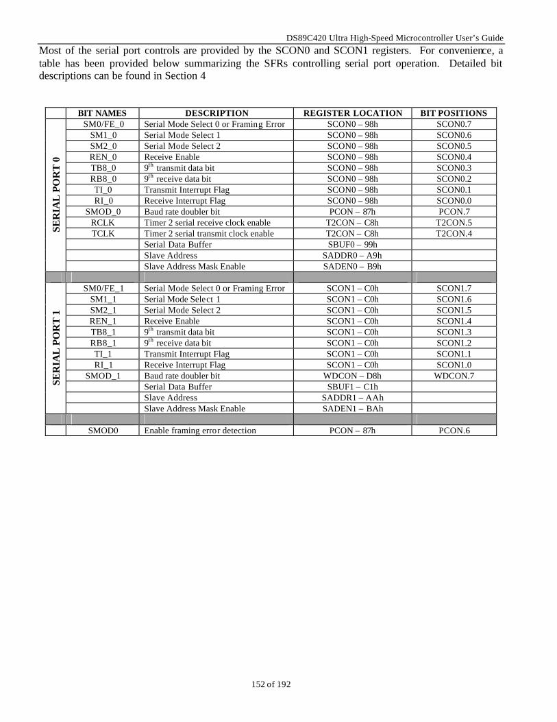
DS89C420 Ultra High-Speed Microcontroller User’s Guide
152 of 192
Most of the serial port controls are provided by the SCON0 and SCON1 registers. For convenience, a table has been provided below summarizing the SFRs controlling serial port operation. Detailed bit descriptions can be found in Section 4
BIT NAMES DESCRIPTION REGISTER LOCATION BIT POSITIONS SM0/FE_0 Serial Mode Select 0 or Framing Error SCON0 – 98h SCON0.7
SM1_0 Serial Mode Select 1 SCON0 – 98h SCON0.6 SM2_0 Serial Mode Select 2 SCON0 – 98h SCON0.5 REN_0 Receive Enable SCON0 – 98h SCON0.4 TB8_0 9th transmit data bit SCON0 – 98h SCON0.3 RB8_0 9th receive data bit SCON0 – 98h SCON0.2 TI_0 Transmit Interrupt Flag SCON0 – 98h SCON0.1 RI_0 Receive Interrupt Flag SCON0 – 98h SCON0.0
SMOD_0 Baud rate doubler bit PCON – 87h PCON.7 RCLK Timer 2 serial receive clock enable T2CON – C8h T2CON.5 TCLK Timer 2 serial transmit clock enable T2CON – C8h T2CON.4
Serial Data Buffer SBUF0 – 99h Slave Address SADDR0 – A9h
SER
IAL
PO
RT
0
Slave Address Mask Enable SADEN0 – B9h
SM0/FE_1 Serial Mode Select 0 or Framing Error SCON1 – C0h SCON1.7 SM1_1 Serial Mode Select 1 SCON1 – C0h SCON1.6 SM2_1 Serial Mode Select 2 SCON1 – C0h SCON1.5 REN_1 Receive Enable SCON1 – C0h SCON1.4 TB8_1 9th transmit data bit SCON1 – C0h SCON1.3 RB8_1 9th receive data bit SCON1 – C0h SCON1.2 TI_1 Transmit Interrupt Flag SCON1 – C0h SCON1.1 RI_1 Receive Interrupt Flag SCON1 – C0h SCON1.0
SMOD_1 Baud rate doubler bit WDCON – D8h WDCON.7 Serial Data Buffer SBUF1 – C1h Slave Address SADDR1 – AAh
SER
IAL
PO
RT
1
Slave Address Mask Enable SADEN1 – BAh SMOD0 Enable framing error detection PCON – 87h PCON.6
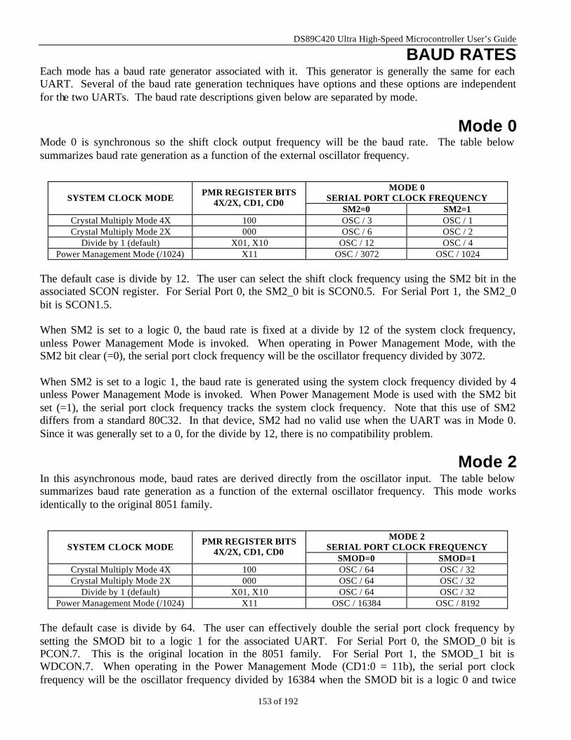
DS89C420 Ultra High-Speed Microcontroller User’s Guide
153 of 192
BAUD RATES Each mode has a baud rate generator associated with it. This generator is generally the same for each UART. Several of the baud rate generation techniques have options and these options are independent for the two UARTs. The baud rate descriptions given below are separated by mode.
Mode 0 Mode 0 is synchronous so the shift clock output frequency will be the baud rate. The table below summarizes baud rate generation as a function of the external oscillator frequency.
MODE 0
SERIAL PORT CLOCK FREQUENCY SYSTEM CLOCK MODE PMR REGISTER BITS
4X/2X, CD1, CD0 SM2=0 SM2=1
Crystal Multiply Mode 4X 100 OSC / 3 OSC / 1 Crystal Multiply Mode 2X 000 OSC / 6 OSC / 2
Divide by 1 (default) X01, X10 OSC / 12 OSC / 4 Power Management Mode (/1024) X11 OSC / 3072 OSC / 1024
The default case is divide by 12. The user can select the shift clock frequency using the SM2 bit in the associated SCON register. For Serial Port 0, the SM2_0 bit is SCON0.5. For Serial Port 1, the SM2_0 bit is SCON1.5. When SM2 is set to a logic 0, the baud rate is fixed at a divide by 12 of the system clock frequency, unless Power Management Mode is invoked. When operating in Power Management Mode, with the SM2 bit clear (=0), the serial port clock frequency will be the oscillator frequency divided by 3072. When SM2 is set to a logic 1, the baud rate is generated using the system clock frequency divided by 4 unless Power Management Mode is invoked. When Power Management Mode is used with the SM2 bit set (=1), the serial port clock frequency tracks the system clock frequency. Note that this use of SM2 differs from a standard 80C32. In that device, SM2 had no valid use when the UART was in Mode 0. Since it was generally set to a 0, for the divide by 12, there is no compatibility problem.
Mode 2 In this asynchronous mode, baud rates are derived directly from the oscillator input. The table below summarizes baud rate generation as a function of the external oscillator frequency. This mode works identically to the original 8051 family.
MODE 2
SERIAL PORT CLOCK FREQUENCY SYSTEM CLOCK MODE PMR REGISTER BITS
4X/2X, CD1, CD0 SMOD=0 SMOD=1
Crystal Multiply Mode 4X 100 OSC / 64 OSC / 32 Crystal Multiply Mode 2X 000 OSC / 64 OSC / 32
Divide by 1 (default) X01, X10 OSC / 64 OSC / 32 Power Management Mode (/1024) X11 OSC / 16384 OSC / 8192
The default case is divide by 64. The user can effectively double the serial port clock frequency by setting the SMOD bit to a logic 1 for the associated UART. For Serial Port 0, the SMOD_0 bit is PCON.7. This is the original location in the 8051 family. For Serial Port 1, the SMOD_1 bit is WDCON.7. When operating in the Power Management Mode (CD1:0 = 11b), the serial port clock frequency will be the oscillator frequency divided by 16384 when the SMOD bit is a logic 0 and twice

DS89C420 Ultra High-Speed Microcontroller User’s Guide
154 of 192
that frequency (OSC / 8192) when the SMOD doubler bit is a logic 1. SMOD bits default to a logic 0 on all resets.
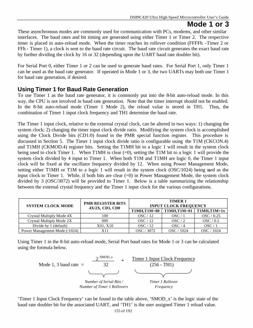
DS89C420 Ultra High-Speed Microcontroller User’s Guide
155 of 192
Mode 1 or 3 These asynchronous modes are commonly used for communication with PCs, modems, and other similar interfaces. The baud rates and bit timing are generated using either Timer 1 or Timer 2. The respective timer is placed in auto-reload mode. When the timer reaches its rollover condition (FFFFh -Timer 2 or FFh - Timer 1), a clock is sent to the baud rate circuit. The baud rate circuit generates the exact baud rate by further dividing the clock by 16 or 32 (depending upon the UART baud rate doubler bit). For Serial Port 0, either Timer 1 or 2 can be used to generate baud rates. For Serial Port 1, only Timer 1 can be used as the baud rate generator. If operated in Mode 1 or 3, the two UARTs may both use Timer 1 for baud rate generation, if desired. Using Timer 1 for Baud Rate Generation To use Timer 1 as the baud rate generator, it is commonly put into the 8-bit auto-reload mode. In this way, the CPU is not involved in baud rate generation. Note that the timer interrupt should not be enabled. In the 8-bit auto-reload mode (Timer 1 Mode 2), the reload value is stored in TH1. Thus, the combination of Timer 1 input clock frequency and TH1 determine the baud rate. The Timer 1 input clock, relative to the external crystal clock, can be altered in two ways: 1) changing the system clock; 2) changing the timer input clock divide ratio. Modifying the system clock is accomplished using the Clock Divide bits (CD1:0) found in the PMR special function register. This procedure is discussed in Section 5. The Timer 1 input clock divide ratio is configurable using the T1M (CKCON.4) and T1MH (CKMOD.4) register bits. Setting the T1MH bit to a logic 1 will result in the system clock being used to clock Timer 1. When T1MH is clear (=0), setting the T1M bit to a logic 1 will provide the system clock divided by 4 input to Timer 1. When both T1M and T1MH are logic 0, the Timer 1 input clock will be fixed at the oscillator frequency divided by 12. When using Power Management Mode, setting either T1MH or T1M to a logic 1 will result in the system clock (OSC/1024) being used as the input clock to Timer 1. While, if both bits are clear (=0) in Power Management Mode, the system clock divided by 3 (OSC/3072) will be provided to Timer 1. Below is a table summarizing the relationship between the external crystal frequency and the Timer 1 input clock for the various configurations.
TIMER 1
INPUT CLOCK FREQUENCY SYSTEM CLOCK MODE PMR REGISTER BITS
4X/2X, CD1, CD0 T1MH,T1M=00 T1MH,T1M=01 T1MH,T1M=1x
Crystal Multiply Mode 4X 100 OSC / 12 OSC / 1 OSC / 0.25 Crystal Multiply Mode 2X 000 OSC / 12 OSC / 2 OSC / 0.5
Divide by 1 (default) X01, X10 OSC / 12 OSC / 4 OSC / 1 Power Management Mode (/1024) X11 OSC / 3072 OSC / 1024 OSC / 1024
Using Timer 1 in the 8-bit auto-reload mode, Serial Port baud rates for Mode 1 or 3 can be calculated using the formula below.
2 SMOD_x Timer 1 Input Clock Frequency Mode 1, 3 baud rate = 32 (256 - TH1) ‘Timer 1 Input Clock Frequency’ can be found in the table above, ‘SMOD_x’ is the logic state of the baud rate doubler bit for the associated UART, and ‘TH1’ is the user assigned Timer 1 reload value.
*
Timer 1 Rollover Frequency
Number of Serial Bits / Number of Timer 1 Rollovers
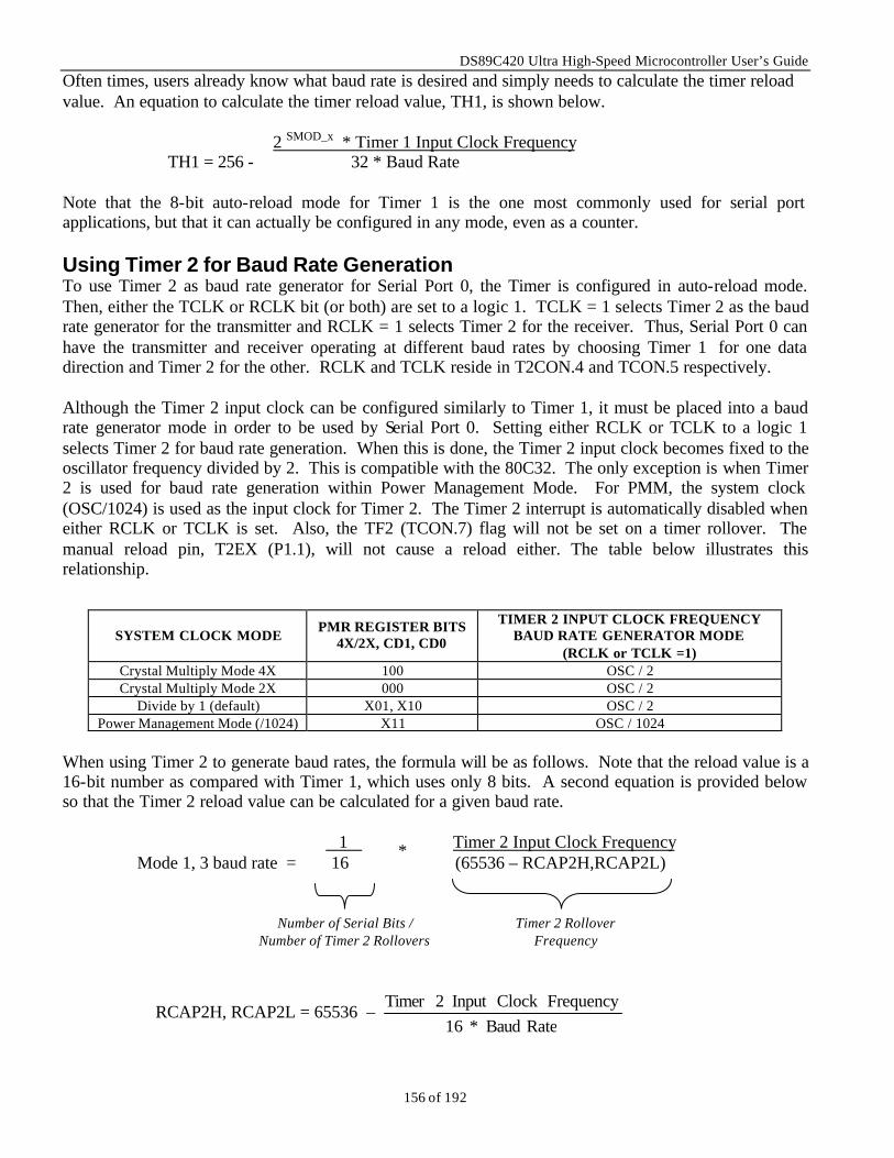
DS89C420 Ultra High-Speed Microcontroller User’s Guide
156 of 192
Often times, users already know what baud rate is desired and simply needs to calculate the timer reload value. An equation to calculate the timer reload value, TH1, is shown below.
2 SMOD_x * Timer 1 Input Clock Frequency TH1 = 256 - 32 * Baud Rate
Note that the 8-bit auto-reload mode for Timer 1 is the one most commonly used for serial port applications, but that it can actually be configured in any mode, even as a counter. Using Timer 2 for Baud Rate Generation To use Timer 2 as baud rate generator for Serial Port 0, the Timer is configured in auto-reload mode. Then, either the TCLK or RCLK bit (or both) are set to a logic 1. TCLK = 1 selects Timer 2 as the baud rate generator for the transmitter and RCLK = 1 selects Timer 2 for the receiver. Thus, Serial Port 0 can have the transmitter and receiver operating at different baud rates by choosing Timer 1 for one data direction and Timer 2 for the other. RCLK and TCLK reside in T2CON.4 and TCON.5 respectively. Although the Timer 2 input clock can be configured similarly to Timer 1, it must be placed into a baud rate generator mode in order to be used by Serial Port 0. Setting either RCLK or TCLK to a logic 1 selects Timer 2 for baud rate generation. When this is done, the Timer 2 input clock becomes fixed to the oscillator frequency divided by 2. This is compatible with the 80C32. The only exception is when Timer 2 is used for baud rate generation within Power Management Mode. For PMM, the system clock (OSC/1024) is used as the input clock for Timer 2. The Timer 2 interrupt is automatically disabled when either RCLK or TCLK is set. Also, the TF2 (TCON.7) flag will not be set on a timer rollover. The manual reload pin, T2EX (P1.1), will not cause a reload either. The table below illustrates this relationship.
SYSTEM CLOCK MODE
PMR REGISTER BITS 4X/2X, CD1, CD0
TIMER 2 INPUT CLOCK FREQUENCY BAUD RATE GENERATOR MODE
(RCLK or TCLK =1) Crystal Multiply Mode 4X 100 OSC / 2 Crystal Multiply Mode 2X 000 OSC / 2
Divide by 1 (default) X01, X10 OSC / 2 Power Management Mode (/1024) X11 OSC / 1024
When using Timer 2 to generate baud rates, the formula will be as follows. Note that the reload value is a 16-bit number as compared with Timer 1, which uses only 8 bits. A second equation is provided below so that the Timer 2 reload value can be calculated for a given baud rate.
1 Timer 2 Input Clock Frequency Mode 1, 3 baud rate = 16 (65536 – RCAP2H,RCAP2L)
RCAP2H, RCAP2L = 65536 – Rate Baud * 16
FrequencyClock Input 2Timer
*
Timer 2 Rollover Frequency
Number of Serial Bits / Number of Timer 2 Rollovers
DS89C420 Ultra High-Speed Microcontroller User’s Guide
157 of 192
‘Timer 2 Input Clock Frequency’ can be found in the table above, and ‘RCAP2H, RCAP2L’ is the user assigned Timer 2 reload value.
SERIAL I/O DESCRIPTION A detailed description and block diagram of each serial mode is given below. Please note that the baud clock input (to the Serial I/O Control block) corresponding to the Power Management Mode has been omitted from each of the block diagrams. Reference the tables earlier in this section for Power Management Mode baud clock rates. A description of framing error detection and multiprocessor communication follows this section.
Mode 0 This mode is used to communicate in synchronous, half–duplex format with devices that accept the Ultra High-Speed Microcontroller as a master. A functional block diagram and basic timing of this mode are shown below. As can be seen, there is one bidirectional data line (RXD) and one shift clock line (TXD) used for communication. The shift clock is used to shift data into and out of the microcontroller and the remote device. Mode 0 requires that the microcontroller is the master because the microcontroller generates the serial shift clocks for both directions. As described earlier in the section, the shift clock frequency is a function of the system clock if the SM2 (SCON0.5 or SCON1.5) bit is set to a logic 1. The RXD signal is used for both transmission and reception. TXD provides the shift clock. Data bits enter and exit least significant bit first. The baud rate is equal to the shift clock frequency. The relevant UART will begin transmitting when any instruction writes to SBUF0 or SBUF1 (address 99h or C1h). The internal shift register will then begin to shift data out. The clock will be activated and will transfer data until the 8-bit value is complete. Data will be presented just prior to the falling edge of the shift clock (TXD) so that an external device can latch the data using the rising edge. The UART will begin to receive data when the REN bit in the SCON register (SCON0.4 or SCON1.4) is set to a logic 1 and the RI bit (SCON0.0 or SCON1.0) is set to a logic 0. This condition tells the UART that there is data to be shifted in. The shift clock (TXD) will activate, and the UART will latch incoming data on the rising edge. The external device should therefore present data on the falling edge. This process will continue unt il 8 bits have been received. The RI bit will automatically be set to a logic 1 immediately following the last rising edge of the shift clock on TXD. This will cause reception to stop until the SBUF has been read, and the RI bit cleared. When RI is cleared, another byte can be shifted in.
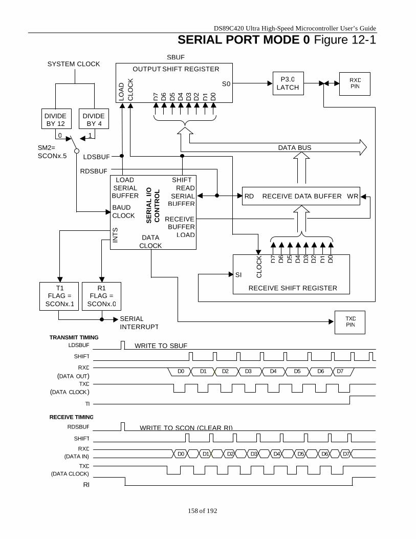
DS89C420 Ultra High-Speed Microcontroller User’s Guide
158 of 192
SERIAL PORT MODE 0 Figure 12-1 SM2= SCONx.5
DIVIDE BY 12
D7
D6
D5
D4
D3
D2
D1
D0
LOA
D
CLO
CK
OUTPUT SHIFT REGISTER
S0 P3.0
LATCH RXD PIN
RECEIVE DATA BUFFER WR RD
D7
D6
D5
D4
D3
D2
D1
D0
CLO
CK
RECEIVE SHIFT REGISTER
SI
READSERIAL
BUFFERBAUD CLOCK
LOAD SERIAL BUFFER
RECEIVEBUFFER
LOADDATA CLOCK
INT
S
SE
RIA
L I/
O
CO
NT
RO
L
SHIFT
R1 FLAG =
SCONx.0
T1 FLAG =
SCONx.1
SERIAL INTERRUPT
DIVIDE BY 4
LDSBUF
RDSBUF
TRANSMIT TIMINGLDSBUF
SHIFT
WRITE TO SBUF
RXD
(DATA OUT)D0 D1 D2 D3 D4 D5 D6 D7
TXD(DATA CLOCK)
TI
RECEIVE TIMING
RDSBUF
SHIFT
WRITE TO SCON (CLEAR RI)
RXD(DATA IN)
TXD(DATA CLOCK)
RI
D0 D1 D2 D3 D4 D5 D6 D7
SBUF
0 1
DATA BUS SM2= SCONx.5
TXD PIN
SYSTEM CLOCK
DS89C420 Ultra High-Speed Microcontroller User’s Guide
159 of 192
Mode 1 This mode is asynchronous, full duplex, using a total of 10 bits. The 10 bits consist of a start bit (logic 0), 8 data bits, and 1 stop bit (logic 1) as illustrated in Figure 12-2. The data is transferred LSb first. As described above, the baud rates for Mode 1 are generated by either a divide by 16 of Timer 1 rollover, a divide by 16 of the Timer 2 rollover, or a divide by 32 of Timer 1 rollover. The UART will begin transmission after the first rollover of the divide by 16 counter following a software write to SBUF. Transmission takes place on the TXD pin. It begins by the start bit being placed on the pin. Data is then shifted out onto the pin, LSb first. The stop bit follows. The TI bit will be set by hardware after the stop bit is placed on the pin. All bits are shifted out at the rate determined by the baud rate generator. Once the baud rate generator is active, reception can begin at any time. The REN bit (SCON0.4 or SCON1.4) must be set to a logic 1 to allow reception. The falling edge of a start bit on the RXD pin will begin the reception process. Data will be shifted in at the selected baud rate. At the middle of the stop bit time, certain conditions must be met to load SBUF with the received data: 1. RI must = 0, and either 2. If SM2 = 0, the state of the stop bit doesn’t matter, or 3. If SM2 = 1, the state of the stop bit must=1. If these conditions are true, then SBUF (hex address 99h or C1h) will be loaded with the received byte, the RB8 bit (SCON0.2 or SCON1.2) will be loaded with the stop bit, and the RI bit (SCON0.0 or SCON1.0) will be set. If these conditions are false, then the received data will be lost (SBUF and RB8 not loaded) and RI will not be set. Regardless of the receive word status, after the middle of the stop bit time, the receiver will go back to looking for a 1 to 0 transition on the RXD pin. Each data bit received is sampled on the 7th, 8th and 9th clock used by the divide by 16 counter. Using majority voting, two equal samples out of the three determines the logic level for each received bit. If the start bit was determined to be invalid (=1), then the receiver goes back to looking for a 1 to 0 transition on the RXD pin in order to start the reception of data.
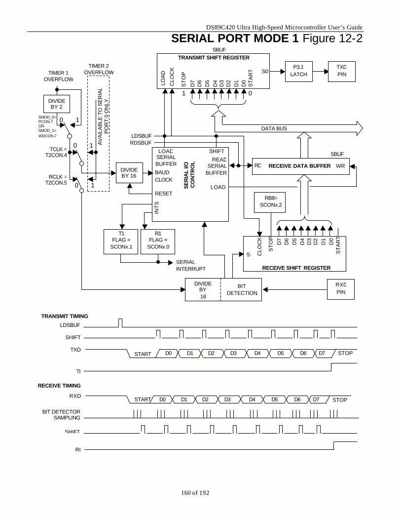
DS89C420 Ultra High-Speed Microcontroller User’s Guide
160 of 192
SERIAL PORT MODE 1 Figure 12-2
SBUF
DIVIDE BY 2
D7 LO
AD
CLO
CK
TRANSMIT SHIFT REGISTER
S0 P3.1
LATCH TXD PIN
RECEIVE DATA BUFFER WR RD
CLO
CK
RECEIVE SHIFT REGISTER
SI
READSERIAL
BUFFERBAUD CLOCK
LOAD SERIAL BUFFER
LOAD
INT
S
SE
RIA
L I/O
C
ON
TR
OL
SHIFT
T1 FLAG =
SCONx.1
RXD PIN
SERIAL INTERRUPT
LDSBUFRDSBUF
ST
OP
ST
AR
T
1 0
ST
OP
ST
AR
T
RB8= SCONx.2
R1 FLAG =
SCONx.0
DIVIDE BY 16
BIT DETECTION
DATA BUS
SBUF
RESET
DIVIDE BY 16
SMOD_0= PCON.7 OR SMOD_1= WDCON.7
D6
D5
D4
D3
D2
D1
D0
D7
D5
D4
D3
D2
D1
D0
D6
TIMER 2 OVERFLOW TIMER 1
OVERFLOW
AV
AIL
AB
LE T
O S
ER
IAL
PO
RT
0 O
NLY
1 0
1 0
1 0
TCLK =T2CON.4
RCLK =T2CON.5
RECEIVE TIMING
BIT DETECTORSAMPLING
SHIFT
RI
RXDD0 D1 D2 D3 D4 D5 D6 D7 STOP START
TRANSMIT TIMING
LDSBUF
SHIFT
TI
TXDD0 D1 D2 D3 D4 D5 D6 D7 STOP START
DS89C420 Ultra High-Speed Microcontroller User’s Guide
161 of 192
Mode 2 This mode uses a total of 11 bits in asynchronous full duplex communication as illustrated in Figure 12-3. The 11 bits consist of one start bit (a logic 0), 8 data bits, a programmable 9th bit, and one stop bit (a logic 1). Like Mode 1, the transmissions occur on the TXD signal pin and receptions on RXD. For transmission purposes, the 9th bit can be stuffed as a logic 0 or 1. A common use is to put the parity bit in this location. The 9th bit is transferred from the TB8 bit position in the SCON register (SCON0.3 or SCON1.3) during the write to SBUF. Baud rates are generated as a fixed function of the crystal frequency as described earlier in this section. Like Mode 1, Mode 2’s transmission begins after the first rollover of the divide by 16 counter following a software write to SBUF. It begins by the start bit being placed on the TXD pin. The data is then shifted out onto the pin LSb first, followed by the 9th bit, and finally the stop bit. The TI bit (SCON0.1 or SCON1.1) is set when the stop bit is placed on the pin. Reception begins when a falling edge is detected as part of the incoming start bit on the RXD pin. The RXD pin is then sampled according to the baud rate speed. The 9th bit is placed in the RB8 bit location in SCON (SCON0.2 or SCON1.2). When a stop bit has been received, the data value will be transferred to the SBUF receive register (hex address 99 or C1). The RI bit (SCON0.0 or SCON1.0) will be set to indicate that a byte has been received. At this time, the UART can receive another byte. Once the baud rate generator is active, reception can begin at any time. The REN bit (SCON0.4 or SCON1.4) must be set to a logic 1 to allow reception. The falling edge of a start bit on the RXD pin will begin the reception process. Data must be shifted in at the selected baud rate. At the middle of the 9th bit time, certain conditions must be met to load SBUF with the received data. 1. RI must = 0, and either 2. If SM2 = 0, the state of the 9th bit doesn’t matter, or 3. If SM2 = 1, the state of the 9th bit must = 1. If these conditions are true, then SBUF will be loaded with the received byte, RB8 will be loaded with the 9th bit, and RI will be set. If these conditions are false, then the received data will be lost (SBUF and RB8 not loaded) and RI will not be set. Regardless of the receive word status, after the middle of the stop bit time, the receiver will go back to looking for a 1 to 0 transition on RXD. Data is sampled in a similar fashion to Mode 1 with the majority voting on three consecutive samples. Mode 2 uses the sample divide by 16 counter with either the oscillator divided by 2 or 4.
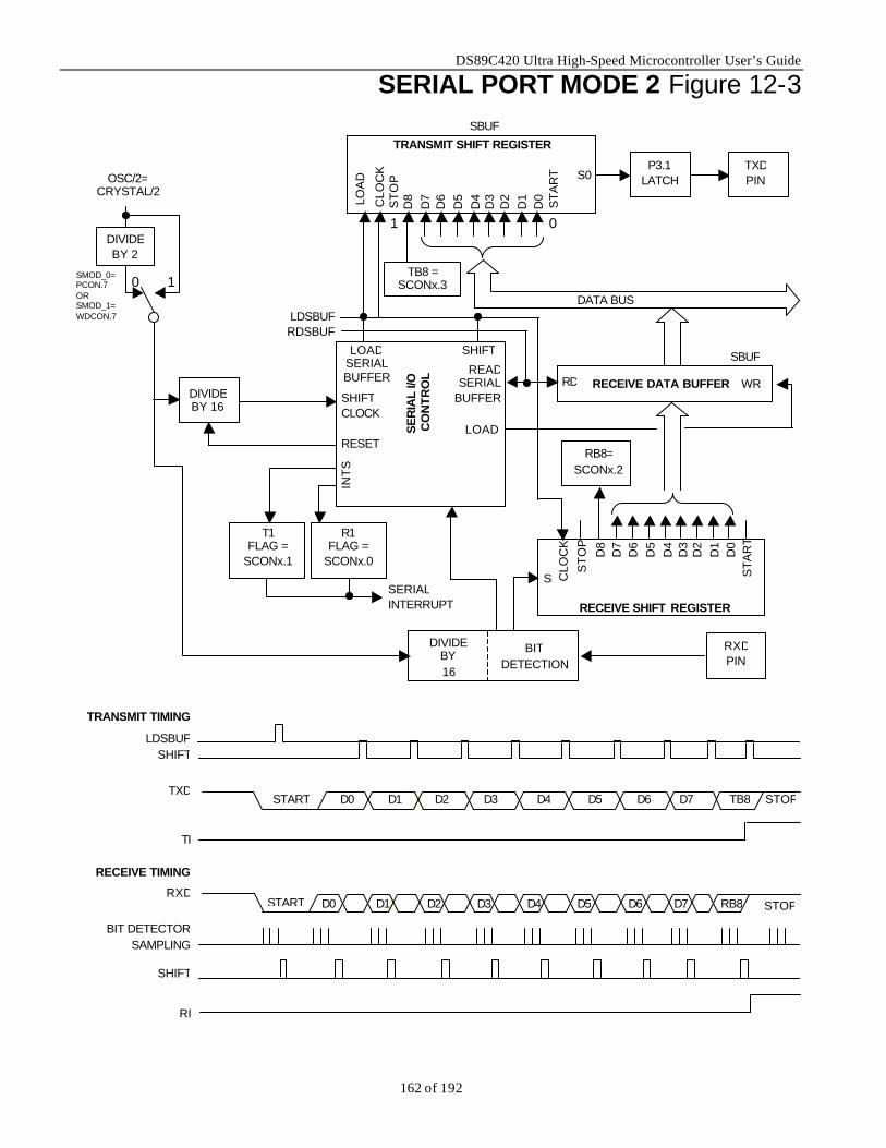
DS89C420 Ultra High-Speed Microcontroller User’s Guide
162 of 192
SERIAL PORT MODE 2 Figure 12-3
SBUF
DIVIDE BY 2
D7 LO
AD
CLO
CK
TRANSMIT SHIFT REGISTER
S0 P3.1
LATCH TXD PIN
RECEIVE DATA BUFFER WR RD
CLO
CK
RECEIVE SHIFT REGISTER
SI
READSERIAL
BUFFERSHIFT CLOCK
LOAD SERIAL BUFFER
LOAD
INT
S
SE
RIA
L I/O
C
ON
TR
OL
SHIFT
T1 FLAG =
SCONx.1
RXD PIN
SERIAL INTERRUPT
LDSBUFRDSBUF
ST
OP
ST
AR
T
1 0
ST
OP
ST
AR
T
RB8= SCONx.2
R1 FLAG =
SCONx.0
DIVIDE BY 16
BIT DETECTION
DATA BUS
SBUF
RESET
DIVIDE BY 16
SMOD_0= PCON.7 OR SMOD_1= WDCON.7
D6
D5
D4
D3
D2
D1
D0
D7
D5
D4
D3
D2
D1
D0
D6
OSC/2= CRYSTAL/2
10
D8
TB8 = SCONx.3
D8
TRANSMIT TIMING
LDSBUFSHIFT
RECEIVE TIMING
BIT DETECTORSAMPLING
SHIFT
TI
RI
TXDD0 D1 D2 D3 D4 D5 D6 D7 STOP START
RXDD0 D1 D2 D3 D4 D5 D6 D7 START STOP
TB8
RB8
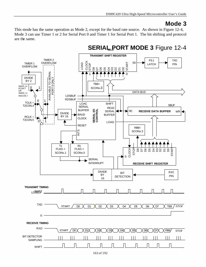
DS89C420 Ultra High-Speed Microcontroller User’s Guide
163 of 192
Mode 3 This mode has the same operation as Mode 2, except for the baud rate source. As shown in Figure 12-4, Mode 3 can use Timer 1 or 2 for Serial Port 0 and Timer 1 for Serial Port 1. The bit shifting and protocol are the same.
SERIAL PORT MODE 3 Figure 12-4
SBUF
DIVIDE BY 2
D7 LO
AD
CLO
CK
TRANSMIT SHIFT REGISTER
S0 P3.1
LATCH TXD PIN
RECEIVE DATA BUFFER WR RD
CLO
CK
RECEIVE SHIFT REGISTER
SI
READSERIAL
BUFFERBAUD CLOCK
LOAD SERIAL BUFFER
LOAD
INT
S
SE
RIA
L I/O
C
ON
TR
OL
SHIFT
T1 FLAG =
SCONx.1
RXD PIN
SERIAL INTERRUPT
LDSBUF RDSBUF
ST
OP
ST
AR
T
1 0
ST
OP
ST
AR
T
RB8= SCONx.3
R1 FLAG =
SCONx.0
DIVIDE BY 16
BIT DETECTION
DATA BUS
SBUF
RESET
DIVIDE BY 16
SMOD_0= PCON.7 OR SMOD_1= WDCON.7
D6
D5
D4
D3
D2
D1
D0
D7
D5
D4
D3
D2
D1
D0
D6
TIMER 2 OVERFLOW TIMER 1
OVERFLOW
AV
AIL
AB
LE T
O S
ER
IAL
PO
RT
0 O
NLY
1 0
1 0
1 0
TCLK =T2CON.4
RCLK =T2CON.5
D8
TB8= SCONx.3
D8
TRANSMIT TIMING
LDSBUF SHIFT
RECEIVE TIMING
BIT DETECTORSAMPLING
SHIFT
TI
TXDD0 D1 D2 D3 D4 D5 D6 D7 STOP START
RXDD0 D1 D2 D3 D4 D5 D6 D7START STOP
TB8
RB8
DS89C420 Ultra High-Speed Microcontroller User’s Guide
164 of 192
FRAMING ERROR DETECTION A framing error occurs when a valid stop bit is not detected. This results in the possible improper reception of the serial word. The UART can detect a framing error and notify the software. Typical causes of framing errors are noise and contention. The Framing Error condition is reported in the SCON register for the corresponding UART. The Framing Error bit, FE, is located in SCON0.7 or SCON1.7. Note that this bit normally serves as SM0 and is described as SM0/FE_0 or SM0/FE_1 in the register description. Framing Error information is made accessible by the SMOD0 Framing Error Detection Enable bit located at PCON.6. When SMOD0 is set to a logic 1, the framing error information is shown in SM0/FE (SCON0.7 or SCON1.7). When SMOD0 is set to a logic 0, the SM0 function is accessible. The information for bits SM0 and FE is actually stored in different registers. Changing SMOD0 only modifies which register is accessed; not the contents of either. The FE bit will be set to a 1 when a framing error occurs. It must be cleared by software. Note that the SMOD0 state must be 1 while reading or writing the FE bit. Also note that receiving a properly framed serial word will not clear the FE bit. This must be done in software.
MULTIPROCESSOR COMMUNICATION Multiprocessor communication mode makes special use of the 9th data bit in Modes 2 and 3. In the original 8051, the 9th bit was restricted to a 0 or 1 condition, but had no special purpose. In the 80C32 and the Ultra High-Speed Microcontroller, it can be used to signify that the incoming byte is an address. This allows the processor to be interrupted only if the correct address appears. If multiprocessor mode has been enabled, the receive interrupt (signaled by the RI bit) will only occur when a recognized address is received. When a serial word is received with the 9th bit set and the appropriate SM2=1, the byte will be assumed to be an address. The address will be compared to an internally stored address. If it matches, a receive interrupt will occur. The internal address is derived from the contents of two registers. The first register specifies an absolute address. This is the user specified address of the device. The second register is a bit masking register that tells the comparator which address bit(s) to actually use in the comparison. This allows broadcast transmissions that reach groups of microcontrollers or all microcontrollers on a serial port. The user defines this protocol. There are two Special Function Registers that support multiprocessor communication for each UART. These are independent, so that different addresses can be used in each. The registers are SADDR0 or SADDR1(hex address A9h or AAh) and SADEN0 or SADEN1 (hex address B9h or BAh). The SADDR register specifies the individual processor’s address. The SADEN identifies address bits that should be ignored in matching addresses. Software will write an 8-bit address to the SADDR register. This is the microcontroller’s individual address. Any bit in SADEN that contains a logic 0 will cause the corresponding bit in SADDR to be ignored in comparison. Thus logic 0 bits in SADEN create don’t care bit states for address comparisons. When an address is received, each address bit that is not masked by a don’t care will be compared to the SADDR. The microcontroller will interrupt on any address that matches this comparison. Any address that meets this comparison is called a Given Address.
RI
DS89C420 Ultra High-Speed Microcontroller User’s Guide
165 of 192
The following example shows how one address can be directed to an individual processor, or two out of three. Micro 1 SADDR 11110000 SADEN 11111010 ––––––––––––––––––––––––– Given 11110x0x Micro 2
SADDR 11110001 SADEN 11111001 ––––––––––––––––––––––––– Given 11110xx1
Micro 3 SADDR 11110010 SADEN 11111010 ––––––––––––––––––––––––– Given 11110x1x
Note that an address of 11110000 will reach only microcontroller 1. An address of 11110001 will reach both microcontroller 1 and microcontroller 2. An address of 11110010 will reach only microcontroller 3. The microcontroller will also match on any address that corresponds to the Broadcast Address. This is the logical OR of the SADDR and SADEN registers, with any 0s defined as don’t cares. In most cases, the Broadcast Address will be FFh. The multiprocessor communication is always enabled. However, the SADEN registers default to 00h, which means all address bits are don’t care, so all match. Thus if no multiprocessor communication is used, these registers can be ignored.
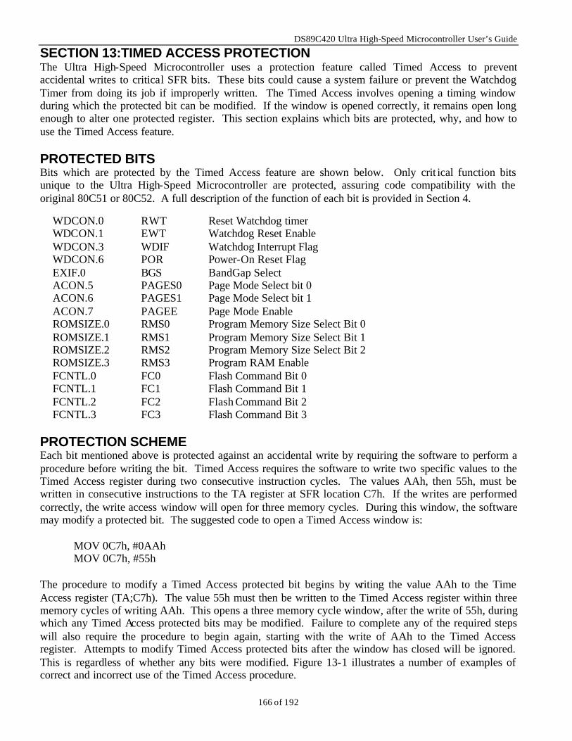
DS89C420 Ultra High-Speed Microcontroller User’s Guide
166 of 192
SECTION 13:TIMED ACCESS PROTECTION The Ultra High-Speed Microcontroller uses a protection feature called Timed Access to prevent accidental writes to critical SFR bits. These bits could cause a system failure or prevent the Watchdog Timer from doing its job if improperly written. The Timed Access involves opening a timing window during which the protected bit can be modified. If the window is opened correctly, it remains open long enough to alter one protected register. This section explains which bits are protected, why, and how to use the Timed Access feature. PROTECTED BITS Bits which are protected by the Timed Access feature are shown below. Only crit ical function bits unique to the Ultra High-Speed Microcontroller are protected, assuring code compatibility with the original 80C51 or 80C52. A full description of the function of each bit is provided in Section 4.
WDCON.0 RWT Reset Watchdog timer WDCON.1 EWT Watchdog Reset Enable WDCON.3 WDIF Watchdog Interrupt Flag WDCON.6 POR Power-On Reset Flag EXIF.0 BGS BandGap Select ACON.5 PAGES0 Page Mode Select bit 0 ACON.6 PAGES1 Page Mode Select bit 1 ACON.7 PAGEE Page Mode Enable ROMSIZE.0 RMS0 Program Memory Size Select Bit 0 ROMSIZE.1 RMS1 Program Memory Size Select Bit 1 ROMSIZE.2 RMS2 Program Memory Size Select Bit 2 ROMSIZE.3 RMS3 Program RAM Enable FCNTL.0 FC0 Flash Command Bit 0 FCNTL.1 FC1 Flash Command Bit 1 FCNTL.2 FC2 Flash Command Bit 2 FCNTL.3 FC3 Flash Command Bit 3
PROTECTION SCHEME Each bit mentioned above is protected against an accidental write by requiring the software to perform a procedure before writing the bit. Timed Access requires the software to write two specific values to the Timed Access register during two consecutive instruction cycles. The values AAh, then 55h, must be written in consecutive instructions to the TA register at SFR location C7h. If the writes are performed correctly, the write access window will open for three memory cycles. During this window, the software may modify a protected bit. The suggested code to open a Timed Access window is: MOV 0C7h, #0AAh
MOV 0C7h, #55h The procedure to modify a Timed Access protected bit begins by writing the value AAh to the Time Access register (TA;C7h). The value 55h must then be written to the Timed Access register within three memory cycles of writing AAh. This opens a three memory cycle window, after the write of 55h, during which any Timed Access protected bits may be modified. Failure to complete any of the required steps will also require the procedure to begin again, starting with the write of AAh to the Timed Access register. Attempts to modify Timed Access protected bits after the window has closed will be ignored. This is regardless of whether any bits were modified. Figure 13-1 illustrates a number of examples of correct and incorrect use of the Timed Access procedure.
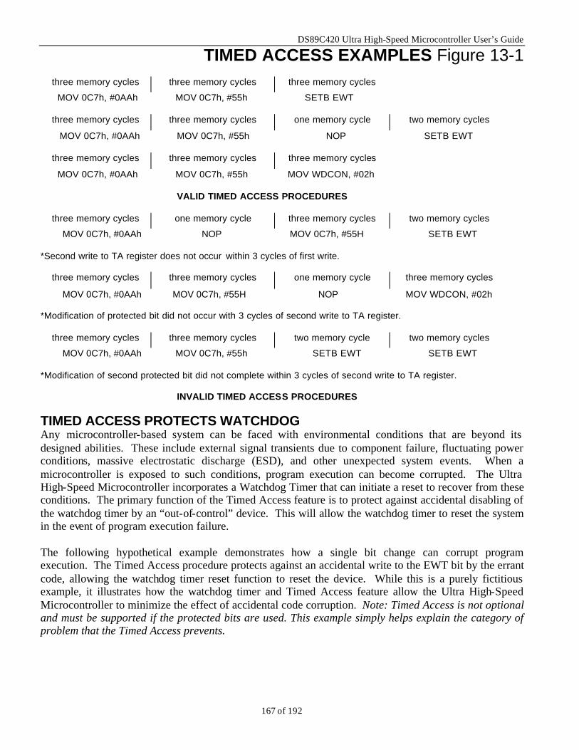
DS89C420 Ultra High-Speed Microcontroller User’s Guide
167 of 192
TIMED ACCESS EXAMPLES Figure 13-1
three memory cycles three memory cycles three memory cycles
MOV 0C7h, #0AAh MOV 0C7h, #55h SETB EWT
three memory cycles three memory cycles one memory cycle two memory cycles
MOV 0C7h, #0AAh MOV 0C7h, #55h NOP SETB EWT
three memory cycles three memory cycles three memory cycles
MOV 0C7h, #0AAh MOV 0C7h, #55h MOV WDCON, #02h VALID TIMED ACCESS PROCEDURES
three memory cycles one memory cycle three memory cycles two memory cycles
MOV 0C7h, #0AAh NOP MOV 0C7h, #55H SETB EWT *Second write to TA register does not occur within 3 cycles of first write.
three memory cycles three memory cycles one memory cycle three memory cycles
MOV 0C7h, #0AAh MOV 0C7h, #55H NOP MOV WDCON, #02h *Modification of protected bit did not occur with 3 cycles of second write to TA register.
three memory cycles three memory cycles two memory cycle two memory cycles
MOV 0C7h, #0AAh MOV 0C7h, #55h SETB EWT SETB EWT *Modification of second protected bit did not complete within 3 cycles of second write to TA register.
INVALID TIMED ACCESS PROCEDURES
TIMED ACCESS PROTECTS WATCHDOG Any microcontroller-based system can be faced with environmental conditions that are beyond its designed abilities. These include external signal transients due to component failure, fluctuating power conditions, massive electrostatic discharge (ESD), and other unexpected system events. When a microcontroller is exposed to such conditions, program execution can become corrupted. The Ultra High-Speed Microcontroller incorporates a Watchdog Timer that can initiate a reset to recover from these conditions. The primary function of the Timed Access feature is to protect against accidental disabling of the watchdog timer by an “out-of-control” device. This will allow the watchdog timer to reset the system in the event of program execution failure. The following hypothetical example demonstrates how a single bit change can corrupt program execution. The Timed Access procedure protects against an accidental write to the EWT bit by the errant code, allowing the watchdog timer reset function to reset the device. While this is a purely fictitious example, it illustrates how the watchdog timer and Timed Access feature allow the Ultra High-Speed Microcontroller to minimize the effect of accidental code corruption. Note: Timed Access is not optional and must be supported if the protected bits are used. This example simply helps explain the category of problem that the Timed Access prevents.
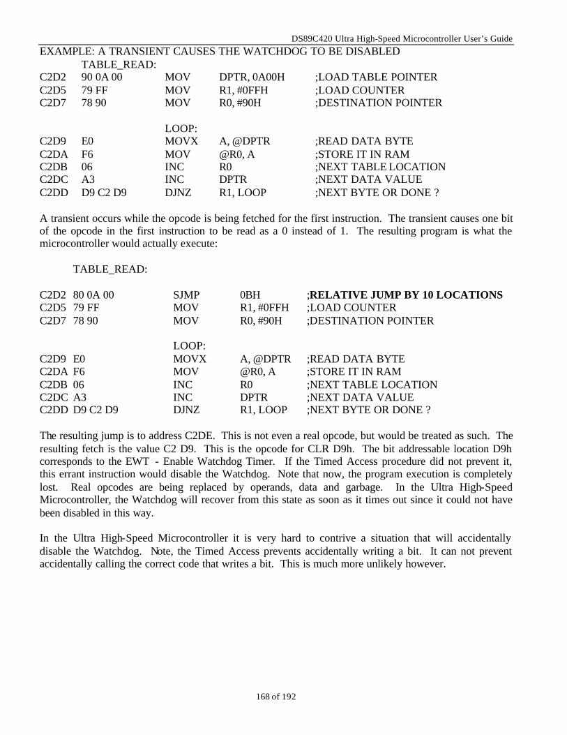
DS89C420 Ultra High-Speed Microcontroller User’s Guide
168 of 192
EXAMPLE: A TRANSIENT CAUSES THE WATCHDOG TO BE DISABLED TABLE_READ: C2D2 90 0A 00 MOV DPTR, 0A00H ;LOAD TABLE POINTER C2D5 79 FF MOV R1, #0FFH ;LOAD COUNTER C2D7 78 90 MOV R0, #90H ;DESTINATION POINTER LOOP: C2D9 E0 MOVX A, @DPTR ;READ DATA BYTE C2DA F6 MOV @R0, A ;STORE IT IN RAM C2DB 06 INC R0 ;NEXT TABLE LOCATION C2DC A3 INC DPTR ;NEXT DATA VALUE C2DD D9 C2 D9 DJNZ R1, LOOP ;NEXT BYTE OR DONE ? A transient occurs while the opcode is being fetched for the first instruction. The transient causes one bit of the opcode in the first instruction to be read as a 0 instead of 1. The resulting program is what the microcontroller would actually execute:
TABLE_READ:
C2D2 80 0A 00 SJMP 0BH ;RELATIVE JUMP BY 10 LOCATIONS C2D5 79 FF MOV R1, #0FFH ;LOAD COUNTER C2D7 78 90 MOV R0, #90H ;DESTINATION POINTER
LOOP: C2D9 E0 MOVX A, @DPTR ;READ DATA BYTE C2DA F6 MOV @R0, A ;STORE IT IN RAM C2DB 06 INC R0 ;NEXT TABLE LOCATION C2DC A3 INC DPTR ;NEXT DATA VALUE C2DD D9 C2 D9 DJNZ R1, LOOP ;NEXT BYTE OR DONE ? The resulting jump is to address C2DE. This is not even a real opcode, but would be treated as such. The resulting fetch is the value C2 D9. This is the opcode for CLR D9h. The bit addressable location D9h corresponds to the EWT - Enable Watchdog Timer. If the Timed Access procedure did not prevent it, this errant instruction would disable the Watchdog. Note that now, the program execution is completely lost. Real opcodes are being replaced by operands, data and garbage. In the Ultra High-Speed Microcontroller, the Watchdog will recover from this state as soon as it times out since it could not have been disabled in this way. In the Ultra High-Speed Microcontroller it is very hard to contrive a situation that will accidentally disable the Watchdog. Note, the Timed Access prevents accidentally writing a bit. It can not prevent accidentally calling the correct code that writes a bit. This is much more unlikely however.
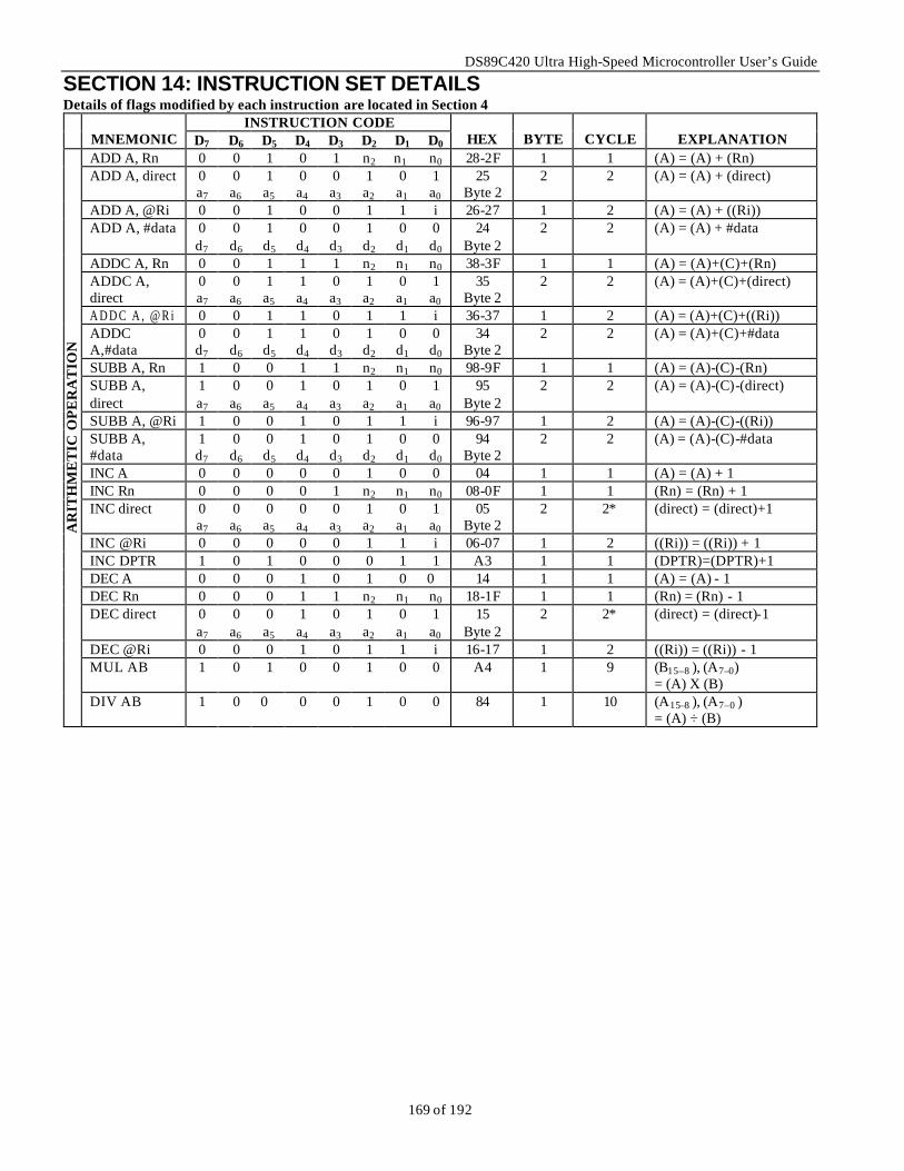
DS89C420 Ultra High-Speed Microcontroller User’s Guide
169 of 192
SECTION 14: INSTRUCTION SET DETAILS Details of flags modified by each instruction are located in Section 4
INSTRUCTION CODE MNEMONIC D7 D6 D5 D4 D3 D2 D1 D0
HEX
BYTE
CYCLE
EXPLANATION
ADD A, Rn 0 0 1 0 1 n2 n1 n0 28-2F 1 1 (A) = (A) + (Rn) ADD A, direct 0
a7 0 a6
1 a5
0 a4
0 a3
1 a2
0 a1
1 a0
25 Byte 2
2 2 (A) = (A) + (direct)
ADD A, @Ri 0 0 1 0 0 1 1 i 26-27 1 2 (A) = (A) + ((Ri)) ADD A, #data 0
d7 0 d6
1 d5
0 d4
0 d3
1 d2
0 d1
0 d0
24 Byte 2
2 2 (A) = (A) + #data
ADDC A, Rn 0 0 1 1 1 n2 n1 n0 38-3F 1 1 (A) = (A)+(C)+(Rn) ADDC A, direct
0 a7
0 a6
1 a5
1 a4
0 a3
1 a2
0 a1
1 a0
35 Byte 2
2 2 (A) = (A)+(C)+(direct)
A D D C A , @ R i 0 0 1 1 0 1 1 i 36-37 1 2 (A) = (A)+(C)+((Ri)) ADDC A,#data
0 d7
0 d6
1 d5
1 d4
0 d3
1 d2
0 d1
0 d0
34 Byte 2
2 2 (A) = (A)+(C)+#data
SUBB A, Rn 1 0 0 1 1 n2 n1 n0 98-9F 1 1 (A) = (A)-(C)-(Rn) SUBB A, direct
1 a7
0 a6
0 a5
1 a4
0 a3
1 a2
0 a1
1 a0
95 Byte 2
2 2 (A) = (A)-(C)-(direct)
SUBB A, @Ri 1 0 0 1 0 1 1 i 96-97 1 2 (A) = (A)-(C)-((Ri)) SUBB A, #data
1 d7
0 d6
0 d5
1 d4
0 d3
1 d2
0 d1
0 d0
94 Byte 2
2 2 (A) = (A)-(C)-#data
INC A 0 0 0 0 0 1 0 0 04 1 1 (A) = (A) + 1 INC Rn 0 0 0 0 1 n2 n1 n0 08-0F 1 1 (Rn) = (Rn) + 1 INC direct 0
a7 0 a6
0 a5
0 a4
0 a3
1 a2
0 a1
1 a0
05 Byte 2
2 2* (direct) = (direct)+1
INC @Ri 0 0 0 0 0 1 1 i 06-07 1 2 ((Ri)) = ((Ri)) + 1 INC DPTR 1 0 1 0 0 0 1 1 A3 1 1 (DPTR)=(DPTR)+1 DEC A 0 0 0 1 0 1 0 0 14 1 1 (A) = (A) - 1 DEC Rn 0 0 0 1 1 n2 n1 n0 18-1F 1 1 (Rn) = (Rn) - 1 DEC direct 0
a7 0 a6
0 a5
1 a4
0 a3
1 a2
0 a1
1 a0
15 Byte 2
2 2* (direct) = (direct)-1
DEC @Ri 0 0 0 1 0 1 1 i 16-17 1 2 ((Ri)) = ((Ri)) - 1 MUL AB 1 0 1 0 0 1 0 0 A4 1 9 (B15–8 ), (A7–0)
= (A) X (B)
AR
ITH
ME
TIC
OP
ER
AT
ION
DIV AB 1 0 0 0 0 1 0 0 84 1 10 (A15–8 ), (A7–0 ) = (A) ÷ (B)
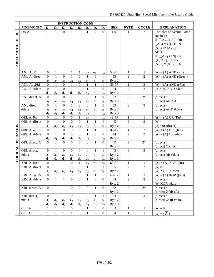
DS89C420 Ultra High-Speed Microcontroller User’s Guide
170 of 192
INSTRUCTION CODE
MNEMONIC D7 D6 D5 D4 D3 D2 D1 D0
HEX
BYTE
CYCLE
EXPLANATION
AR
ITH
ME
TIC
OP
ER
. DA A
1 1 0 1 0 1 0 0 D4 1 2 Contents of Accumulator are BCD, IF [[(A3-0 ) > 9] OR [(AC) = 1]] THEN (A3-0 ) = (A3-0 ) + 6 AND IF [[(A7-4 ) > 9] OR [(C) = 1]] THEN (A7-4 ) = (A7-4 ) + 6
ANL A, Rn 0 1 0 1 1 n2 n1 n0 58-5F 1 1 (A) = (A) AND (Rn) ANL A, direct 0
a7 1 a6
0 a5
1 a4
0 a3
1 a2
0 a1
i a0
55 Byte 2
2 2 (A) = (A) AND (direct)
ANL A, @Ri 0 1 0 1 0 1 1 i 56-57 1 2 (A) = (A) AND ((Ri)) ANL A, #data 0
d7 1 d6
0 d5
1 d4
0 d3
1 d2
0 d1
0 d0
54 Byte 2
2 2 (A)=(A) AND #data
ANL direct, A 0 a7
1 a6
0 a5
1 a4
0 a3
0 a2
1 a1
0 a0
52 Byte 2
2 2* (direct) = (direct) AND A
ANL direct, #data
0 a7 d7
1 a6 d6
0 a5 d5
1 a4 d4
0 a3 d3
0 a2 d2
1 a1 d1
1 a0 d0
53 Byte 2 Byte 3
3 3 (direct) = (direct) AND #data
ORL A, Rn 0 1 0 0 1 n2 n1 n0 48-4F 1 1 (A) = (A) OR (Rn) ORL A, direct 0
a7 1 a6
0 a5
0 a4
0 a3
1 a2
1 a1
I a0
45 Byte 2
2 2 (A) = (A) OR (direct)
ORL A, @Ri 0 1 0 0 0 1 1 i 46-47 1 2 (A) = (A) OR ((Ri)) ORL A, #data 0
d7 1 d6
0 d5
0 d4
0 d3
1 d2
0 d1
0 d0
44 Byte 2
2 2 (A) = (A) OR #data
ORL direct, A 0 1 0 0 0 0 1 0 42 Byte 2
2 2* (direct) = (direct) OR (A)
ORL direct, #data
0 a7 d7
1 a6 d6
0 a5 d5
0 a4 d4
0 a3 d3
0 a2 d2
1 a1 d1
1 a0 d0
43 Byte 2 Byte 3
3 3 (direct) = (direct) OR #data
XRL A, Rn 0 1 1 0 1 n2 n1 n0 68-6F 1 1 (A) = (A) XOR (Rn) XRL A, direct 0
a7 1 a6
1 a5
0 a4
0 a3
1 a2
0 a1
1 a0
65 Byte 2
2 2 (A) = (A) XOR (direct)
XRL A, @ Ri 0 1 1 0 0 1 1 i 66-67 1 2 (A) = (A) XOR ((Ri)) XRL A, #data 0 1 1 0 0 1 0 0 64
Byte 2 2 2 (direct) =
(A) XOR #data XRL direct, A 0 1 1 0 0 0 1 0 62
Byte 2 2 2* (direct) =
(direct) XOR (A) XRL direct, #data
0 a7 d7
1 a6 d6
1 a5 d5
0 a4 d4
0 a3 d3
0 a2 d2
1 a1
d1
1 a0 d0
63 Byte 2 Byte 3
3 3 (direct) = (direct) XOR #data
CLR A 1 1 1 0 0 1 0 0 E4 1 1 (A) = 0
LO
GIC
AL
OP
ER
AT
ION
CPL A 1 1 1 1 0 1 0 0 F4 1 1 (A) = ( A )
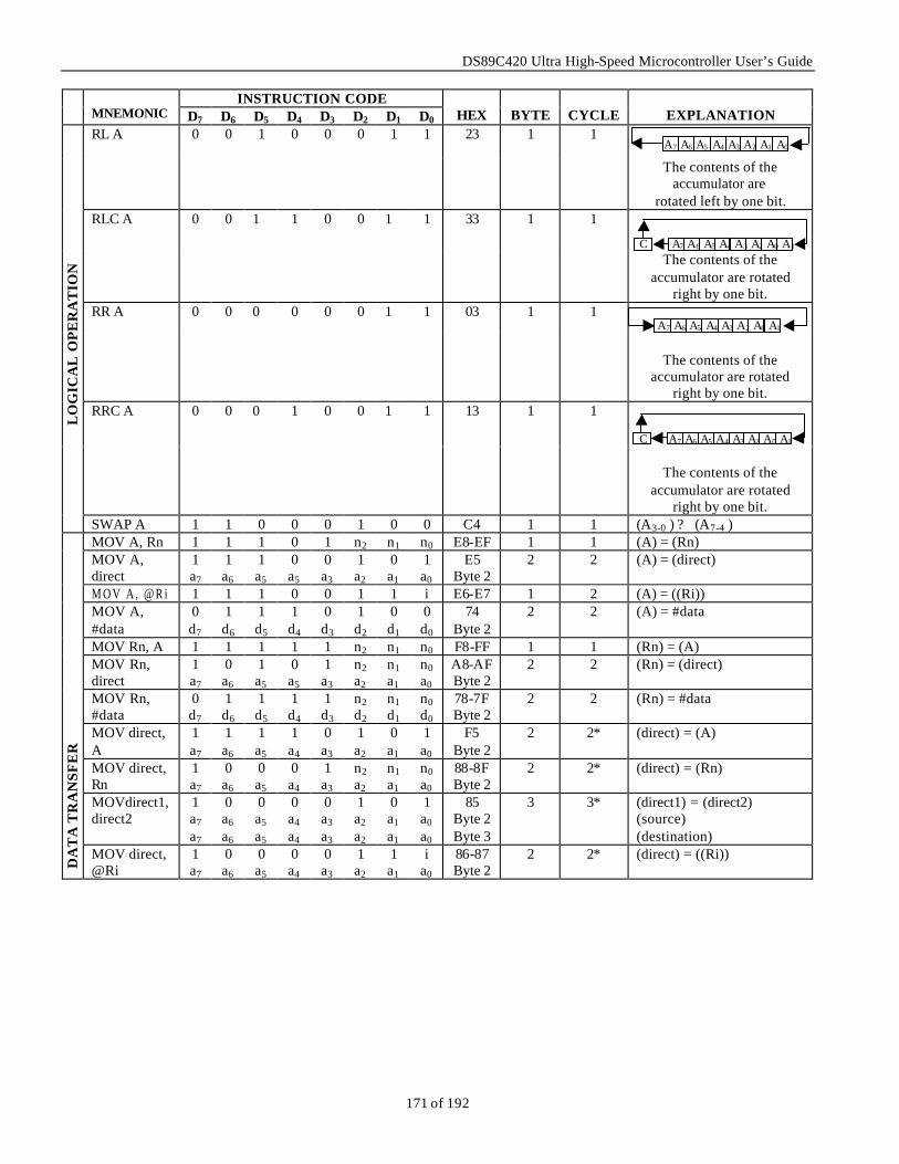
DS89C420 Ultra High-Speed Microcontroller User’s Guide
171 of 192
INSTRUCTION CODE
MNEMONIC D7 D6 D5 D4 D3 D2 D1 D0
HEX
BYTE
CYCLE
EXPLANATION
RL A
0 0 1 0 0 0 1 1 23 1 1 A7 A6 A5 A4 A3 A2 A1 A0
The contents of the accumulator are
rotated left by one bit. RLC A 0 0 1 1 0 0 1 1 33 1 1
C A7 A6 A5 A4 A3 A2 A0 A1
The contents of the accumulator are rotated
right by one bit. RR A 0 0 0 0 0 0 1 1 03 1 1
A7 A6 A5 A4 A3 A2 A0 A1
The contents of the accumulator are rotated
right by one bit. RRC A 0 0 0 1 0 0 1 1 13 1 1
C A7 A6 A5 A4 A3 A2 A0 A1
The contents of the
accumulator are rotated right by one bit.
LO
GIC
AL
OP
ER
AT
ION
SWAP A 1 1 0 0 0 1 0 0 C4 1 1 (A3-0 ) ? (A7-4 ) MOV A, Rn 1 1 1 0 1 n2 n1 n0 E8-EF 1 1 (A) = (Rn) MOV A, direct
1 a7
1 a6
1 a5
0 a5
0 a3
1 a2
0 a1
1 a0
E5 Byte 2
2 2 (A) = (direct)
M O V A , @ R i 1 1 1 0 0 1 1 i E6-E7 1 2 (A) = ((Ri)) MOV A, #data
0 d7
1 d6
1 d5
1 d4
0 d3
1 d2
0 d1
0 d0
74 Byte 2
2 2 (A) = #data
MOV Rn, A 1 1 1 1 1 n2 n1 n0 F8-FF 1 1 (Rn) = (A) MOV Rn, direct
1 a7
0 a6
1 a5
0 a5
1 a3
n2 a2
n1 a1
n0 a0
A8-AF Byte 2
2 2 (Rn) = (direct)
MOV Rn, #data
0 d7
1 d6
1 d5
1 d4
1 d3
n2 d2
n1 d1
n0 d0
78-7F Byte 2
2 2 (Rn) = #data
MOV direct, A
1 a7
1 a6
1 a5
1 a4
0 a3
1 a2
0 a1
1 a0
F5 Byte 2
2 2* (direct) = (A)
MOV direct, Rn
1 a7
0 a6
0 a5
0 a4
1 a3
n2 a2
n1 a1
n0 a0
88-8F Byte 2
2 2* (direct) = (Rn)
MOVdirect1, direct2
1 a7 a7
0 a6 a6
0 a5 a5
0 a4 a4
0 a3 a3
1 a2 a2
0 a1 a1
1 a0 a0
85 Byte 2 Byte 3
3 3* (direct1) = (direct2) (source) (destination)
DA
TA
TR
AN
SFE
R
MOV direct, @Ri
1 a7
0 a6
0 a5
0 a4
0 a3
1 a2
1 a1
i a0
86-87 Byte 2
2 2* (direct) = ((Ri))
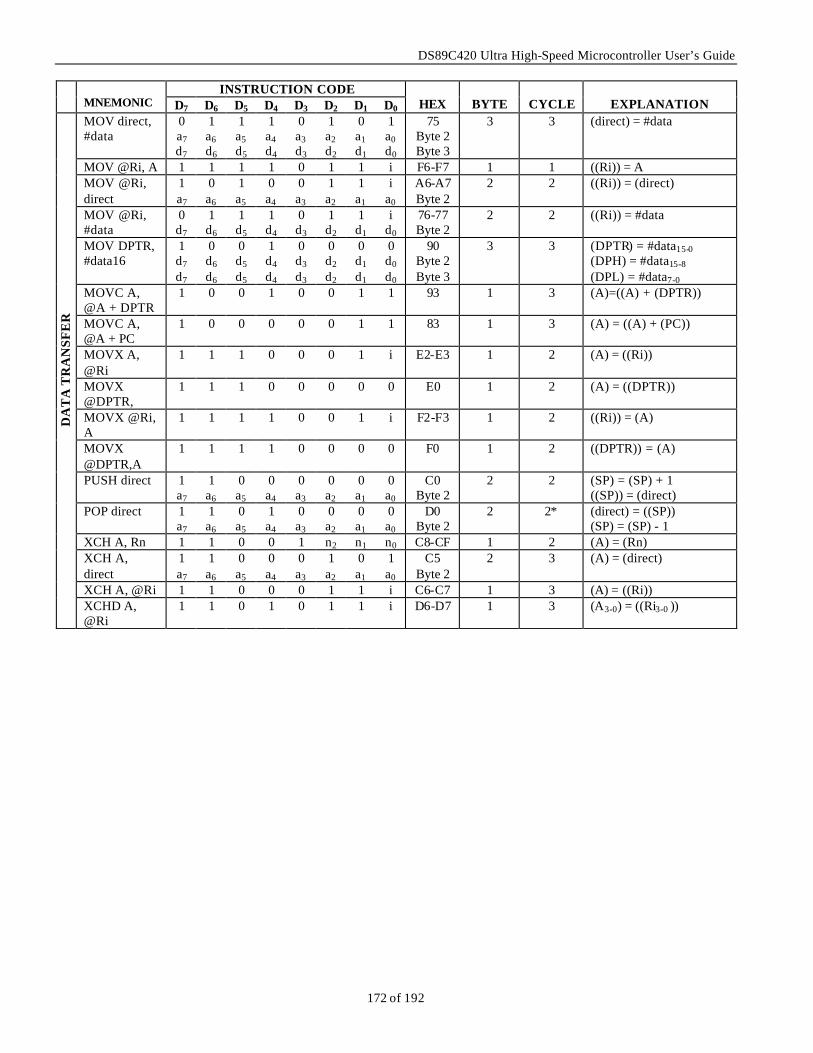
DS89C420 Ultra High-Speed Microcontroller User’s Guide
172 of 192
INSTRUCTION CODE
MNEMONIC D7 D6 D5 D4 D3 D2 D1 D0
HEX
BYTE
CYCLE
EXPLANATION MOV direct, #data
0 a7 d7
1 a6 d6
1 a5 d5
1 a4 d4
0 a3 d3
1 a2 d2
0 a1 d1
1 a0 d0
75 Byte 2 Byte 3
3 3 (direct) = #data
MOV @Ri, A 1 1 1 1 0 1 1 i F6-F7 1 1 ((Ri)) = A MOV @Ri, direct
1 a7
0 a6
1 a5
0 a4
0 a3
1 a2
1 a1
i a0
A6-A7 Byte 2
2 2 ((Ri)) = (direct)
MOV @Ri, #data
0 d7
1 d6
1 d5
1 d4
0 d3
1 d2
1 d1
i d0
76-77 Byte 2
2 2 ((Ri)) = #data
MOV DPTR, #data16
1 d7 d7
0 d6 d6
0 d5 d5
1 d4 d4
0 d3 d3
0 d2 d2
0 d1 d1
0 d0 d0
90 Byte 2 Byte 3
3 3 (DPTR) = #data15-0 (DPH) = #data15-8 (DPL) = #data7-0
MOVC A, @A + DPTR
1 0 0 1 0 0 1 1 93 1 3 (A)=((A) + (DPTR))
MOVC A, @A + PC
1 0 0 0 0 0 1 1 83 1 3 (A) = ((A) + (PC))
MOVX A, @Ri
1 1 1 0 0 0 1 i E2-E3 1 2 (A) = ((Ri))
MOVX @DPTR,
1 1 1 0 0 0 0 0 E0 1 2 (A) = ((DPTR))
MOVX @Ri, A
1 1 1 1 0 0 1 i F2-F3 1 2 ((Ri)) = (A)
MOVX @DPTR,A
1 1 1 1 0 0 0 0 F0 1 2 ((DPTR)) = (A)
PUSH direct 1 a7
1 a6
0 a5
0 a4
0 a3
0 a2
0 a1
0 a0
C0 Byte 2
2 2 (SP) = (SP) + 1 ((SP)) = (direct)
POP direct 1 a7
1 a6
0 a5
1 a4
0 a3
0 a2
0 a1
0 a0
D0 Byte 2
2 2* (direct) = ((SP)) (SP) = (SP) - 1
XCH A, Rn 1 1 0 0 1 n2 n1 n0 C8-CF 1 2 (A) = (Rn) XCH A, direct
1 a7
1 a6
0 a5
0 a4
0 a3
1 a2
0 a1
1 a0
C5 Byte 2
2 3 (A) = (direct)
XCH A, @Ri 1 1 0 0 0 1 1 i C6-C7 1 3 (A) = ((Ri))
DA
TA
TR
AN
SFE
R
XCHD A, @Ri
1 1 0 1 0 1 1 i D6-D7 1 3 (A3-0) = ((Ri3-0 ))
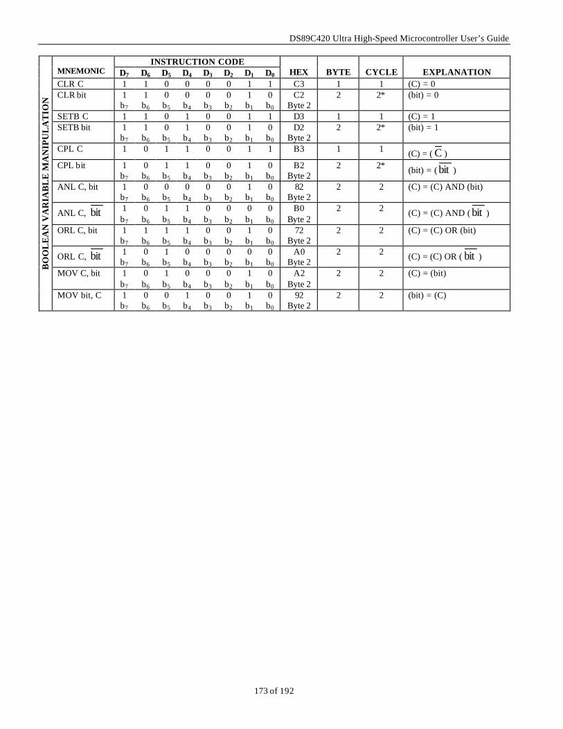
DS89C420 Ultra High-Speed Microcontroller User’s Guide
173 of 192
INSTRUCTION CODE
MNEMONIC D7 D6 D5 D4 D3 D2 D1 D0
HEX
BYTE
CYCLE
EXPLANATION CLR C 1 1 0 0 0 0 1 1 C3 1 1 (C) = 0 CLR bit 1
b7 1 b6
0 b5
0 b4
0 b3
0 b2
1 b1
0 b0
C2 Byte 2
2 2* (bit) = 0
SETB C 1 1 0 1 0 0 1 1 D3 1 1 (C) = 1 SETB bit 1
b7 1 b6
0 b5
1 b4
0 b3
0 b2
1 b1
0 b0
D2 Byte 2
2 2* (bit) = 1
CPL C 1 0 1 1 0 0 1 1 B3 1 1 (C) = ( C ) CPL bit 1
b7 0 b6
1 b5
1 b4
0 b3
0 b2
1 b1
0 b0
B2 Byte 2
2 2* (bit) = ( bit )
ANL C, bit 1 b7
0 b6
0 b5
0 b4
0 b3
0 b2
1 b1
0 b0
82 Byte 2
2 2 (C) = (C) AND (bit)
ANL C, bit 1 b7
0 b6
1 b5
1 b4
0 b3
0 b2
0 b1
0 b0
B0 Byte 2
2 2 (C) = (C) AND ( bit )
ORL C, bit 1 b7
1 b6
1 b5
1 b4
0 b3
0 b2
1 b1
0 b0
72 Byte 2
2 2 (C) = (C) OR (bit)
ORL C, bit 1 b7
0 b6
1 b5
0 b4
0 b3
0 b2
0 b1
0 b0
A0 Byte 2
2 2 (C) = (C) OR ( bit )
MOV C, bit 1 b7
0 b6
1 b5
0 b4
0 b3
0 b2
1 b1
0 b0
A2 Byte 2
2 2 (C) = (bit)
BO
OL
EA
N V
AR
IAB
LE
MA
NIP
UL
AT
ION
MOV bit, C 1 b7
0 b6
0 b5
1 b4
0 b3
0 b2
1 b1
0 b0
92 Byte 2
2 2 (bit) = (C)
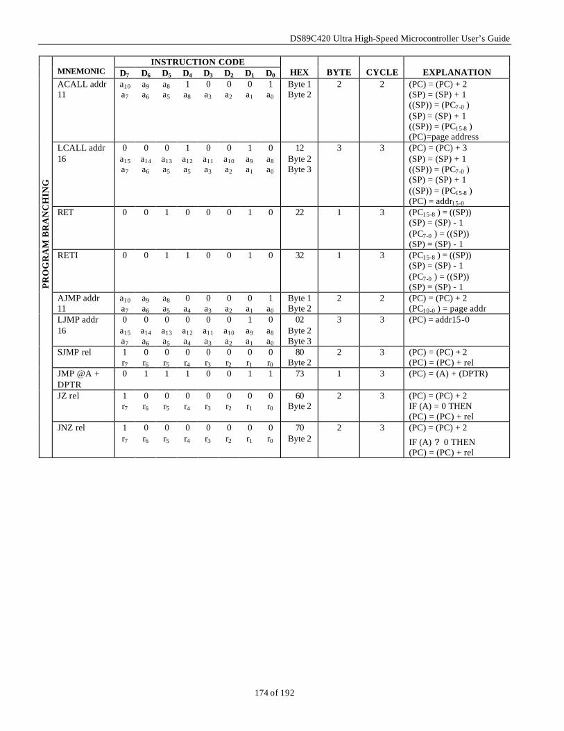
DS89C420 Ultra High-Speed Microcontroller User’s Guide
174 of 192
INSTRUCTION CODE
MNEMONIC D7 D6 D5 D4 D3 D2 D1 D0
HEX
BYTE
CYCLE
EXPLANATION ACALL addr 11
a10 a7
a9 a6
a8 a5
1 a8
0 a3
0 a2
0 a1
1 a0
Byte 1 Byte 2
2 2 (PC) = (PC) + 2 (SP) = (SP) + 1 ((SP)) = (PC7-0 ) (SP) = (SP) + 1 ((SP)) = (PC15-8 ) (PC)=page address
LCALL addr 16
0 a15 a7
0 a14 a6
0 a13 a5
1 a12 a5
0 a11 a3
0 a10 a2
1 a9 a1
0 a8 a0
12 Byte 2 Byte 3
3 3 (PC) = (PC) + 3 (SP) = (SP) + 1 ((SP)) = (PC7-0 ) (SP) = (SP) + 1 ((SP)) = (PC15-8 ) (PC) = addr15-0
RET 0 0 1 0 0 0 1 0 22 1 3 (PC15-8 ) = ((SP)) (SP) = (SP) - 1 (PC7-0 ) = ((SP)) (SP) = (SP) - 1
RETI 0 0 1 1 0 0 1 0 32 1 3 (PC15-8 ) = ((SP)) (SP) = (SP) - 1 (PC7-0 ) = ((SP)) (SP) = (SP) - 1
AJMP addr 11
a10 a7
a9 a6
a8 a5
0 a4
0 a3
0 a2
0 a1
1 a0
Byte 1 Byte 2
2 2 (PC) = (PC) + 2 (PC10-0 ) = page addr
LJMP addr 16
0 a15 a7
0 a14 a6
0 a13 a5
0 a12 a4
0 a11 a3
0 a10 a2
1 a9 a1
0 a8 a0
02 Byte 2 Byte 3
3 3 (PC) = addr15-0
SJMP rel 1 r7
0 r6
0 r5
0 r4
0 r3
0 r2
0 r1
0 r0
80 Byte 2
2 3 (PC) = (PC) + 2 (PC) = (PC) + rel
JMP @A + DPTR
0 1 1 1 0 0 1 1 73 1 3 (PC) = (A) + (DPTR)
JZ rel 1 r7
0 r6
0 r5
0 r4
0 r3
0 r2
0 r1
0 r0
60 Byte 2
2 3 (PC) = (PC) + 2 IF (A) = 0 THEN (PC) = (PC) + rel
P
RO
GR
AM
BR
AN
CH
ING
JNZ rel 1 r7
0 r6
0 r5
0 r4
0 r3
0 r2
0 r1
0 r0
70 Byte 2
2 3 (PC) = (PC) + 2
IF (A) ? 0 THEN (PC) = (PC) + rel
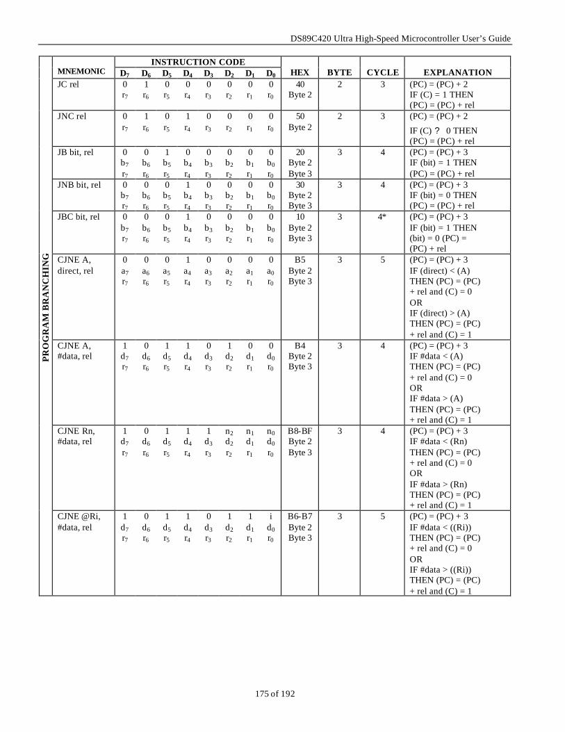
DS89C420 Ultra High-Speed Microcontroller User’s Guide
175 of 192
INSTRUCTION CODE
MNEMONIC D7 D6 D5 D4 D3 D2 D1 D0
HEX
BYTE
CYCLE
EXPLANATION JC rel 0
r7 1 r6
0 r5
0 r4
0 r3
0 r2
0 r1
0 r0
40 Byte 2
2 3 (PC) = (PC) + 2 IF (C) = 1 THEN (PC) = (PC) + rel
JNC rel 0 r7
1 r6
0 r5
1 r4
0 r3
0 r2
0 r1
0 r0
50 Byte 2
2 3 (PC) = (PC) + 2
IF (C) ? 0 THEN (PC) = (PC) + rel
JB bit, rel 0 b7
r7
0 b6
r6
1 b5
r5
0 b4
r4
0 b3
r3
0 b2
r2
0 b1
r1
0 b0
r0
20 Byte 2 Byte 3
3 4 (PC) = (PC) + 3 IF (bit) = 1 THEN (PC) = (PC) + rel
JNB bit, rel 0 b7 r7
0 b6 r6
0 b5 r5
1 b4 r4
0 b3 r3
0 b2 r2
0 b1 r1
0 b0 r0
30 Byte 2 Byte 3
3 4 (PC) = (PC) + 3 IF (bit) = 0 THEN (PC) = (PC) + rel
JBC bit, rel 0 b7 r7
0 b6 r6
0 b5 r5
1 b4 r4
0 b3 r3
0 b2 r2
0 b1 r1
0 b0 r0
10 Byte 2 Byte 3
3 4* (PC) = (PC) + 3 IF (bit) = 1 THEN (bit) = 0 (PC) = (PC) + rel
CJNE A, direct, rel
0 a7 r7
0 a6 r6
0 a5 r5
1 a4 r4
0 a3 r3
0 a2 r2
0 a1 r1
0 a0 r0
B5 Byte 2 Byte 3
3 5 (PC) = (PC) + 3 IF (direct) < (A) THEN (PC) = (PC) + rel and (C) = 0 OR IF (direct) > (A) THEN (PC) = (PC) + rel and (C) = 1
CJNE A, #data, rel
1 d7 r7
0 d6 r6
1 d5 r5
1 d4 r4
0 d3 r3
1 d2 r2
0 d1 r1
0 d0 r0
B4 Byte 2 Byte 3
3 4 (PC) = (PC) + 3 IF #data < (A) THEN (PC) = (PC) + rel and (C) = 0 OR IF #data > (A) THEN (PC) = (PC) + rel and (C) = 1
CJNE Rn, #data, rel
1 d7
r7
0 d6
r6
1 d5
r5
1 d4
r4
1 d3
r3
n2 d2
r2
n1 d1
r1
n0 d0
r0
B8-BF Byte 2 Byte 3
3 4 (PC) = (PC) + 3 IF #data < (Rn) THEN (PC) = (PC) + rel and (C) = 0 OR IF #data > (Rn) THEN (PC) = (PC) + rel and (C) = 1
P
RO
GR
AM
BR
AN
CH
ING
CJNE @Ri, #data, rel
1 d7 r7
0 d6 r6
1 d5 r5
1 d4 r4
0 d3 r3
1 d2 r2
1 d1 r1
i d0 r0
B6-B7 Byte 2 Byte 3
3 5 (PC) = (PC) + 3 IF #data < ((Ri)) THEN (PC) = (PC) + rel and (C) = 0 OR IF #data > ((Ri)) THEN (PC) = (PC) + rel and (C) = 1
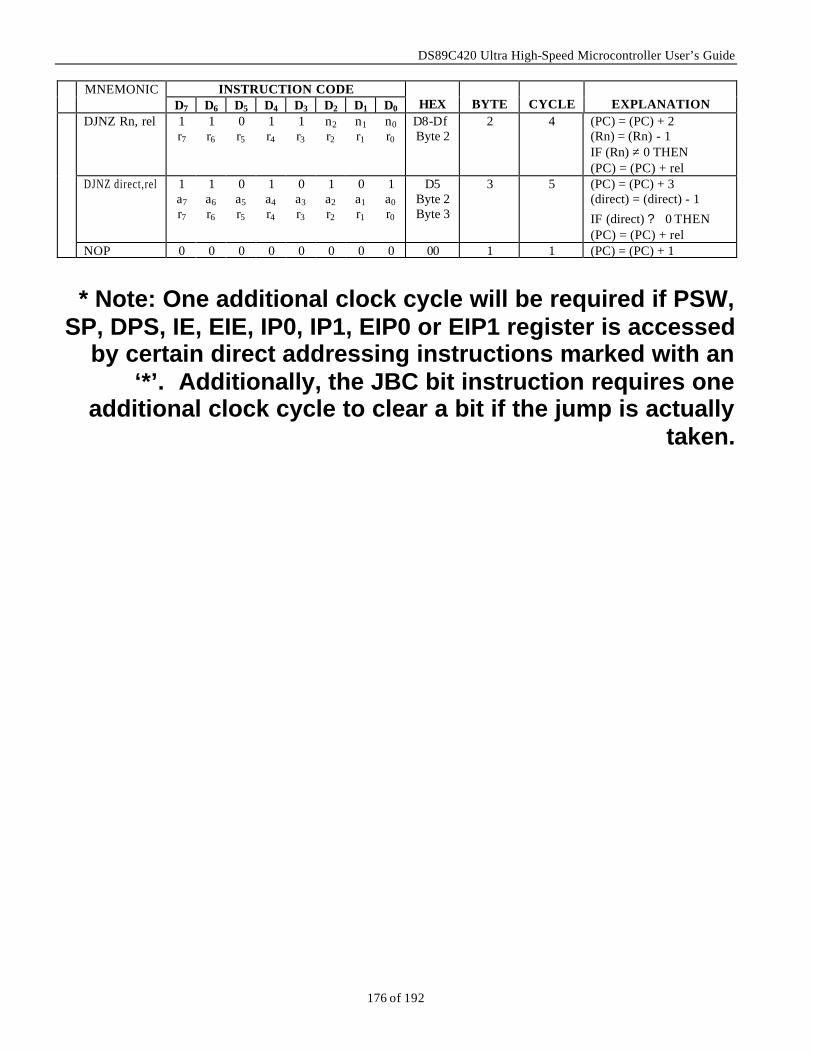
DS89C420 Ultra High-Speed Microcontroller User’s Guide
176 of 192
MNEMONIC INSTRUCTION CODE D7 D6 D5 D4 D3 D2 D1 D0
HEX
BYTE
CYCLE
EXPLANATION
DJNZ Rn, rel 1 r7
1 r6
0 r5
1 r4
1 r3
n2 r2
n1 r1
n0 r0
D8-Df Byte 2
2 4 (PC) = (PC) + 2 (Rn) = (Rn) - 1 IF (Rn) ≠ 0 THEN (PC) = (PC) + rel
DJNZ direct,rel 1 a7 r7
1 a6 r6
0 a5 r5
1 a4 r4
0 a3 r3
1 a2 r2
0 a1 r1
1 a0 r0
D5 Byte 2 Byte 3
3 5 (PC) = (PC) + 3 (direct) = (direct) - 1
IF (direct) ? 0 THEN (PC) = (PC) + rel
NOP 0 0 0 0 0 0 0 0 00 1 1 (PC) = (PC) + 1
* Note: One additional clock cycle will be required if PSW,
SP, DPS, IE, EIE, IP0, IP1, EIP0 or EIP1 register is accessed by certain direct addressing instructions marked with an
‘*’. Additionally, the JBC bit instruction requires one additional clock cycle to clear a bit if the jump is actually
taken.
DS89C420 Ultra High-Speed Microcontroller User’s Guide
177 of 192
SECTION 15: PROGRAM LOADING INTRODUCTION The DS89C420 family has the ability to perform program loading or reloading in a number of ways. First, ROM Loader Mode can be invoked to create a serial communication channel, which permits in-system program/erase of the internal and external program memory. Secondly, Parallel Programming Mode allows programming and erasure of the internal flash memory using industry standard EPROM or flash parallel programmers. Lastly, user code In-application programming allows the capability to in-application erase and reprogram the upper 8K block of flash memory via a special function register interface. Note: The terms ROM Loader, Serial Loader and Bootstrap Loader are used interchangeably in this section and refer to the same functional entity.
DS89C420 Ultra High-Speed Microcontroller User’s Guide
178 of 192
ROM LOADER MODE The DS89C420 defaults to the normal operating (non- loader) mode without external hardware. ROM Loader mode can be invoked at any time as described later in this section. Once the Loader session is complete, the device will perform a hardware reset and begin operation. This will be identical to an external reset, except that the ROM loader, during the loader session, may modify locations in scratchpad RAM in order to execute properly. The following table shows which areas of scratchpad RAM are guaranteed preserved and which ones will be of indeterminate state after exiting the loader. DS89C420
scratchpad memory Guaranteed Preserved 80h - FFh Indeterminate 00h – 7Fh
The guaranteed preserved locations are areas in scratchpad RAM that will not be changed by the bootstrap loader. The indeterminate area contains various stacks and buffers used by the loader, and a given byte in this area may or may not be modified by the loader. As such the user should not rely on the loader preserving any data in this area. It should also be noted that the loader, upon being invoked, clears the EWT bit (WDCON.1) so that the watchdog timer is prevented from generating an internal reset during the loader session. Invoking the ROM Loader Mode The ROM Loader mode is invoked by simultaneously applying a logic 1 to the RST pin, a logic 0 to the EA pin and driving the PSEN pin to a logic 0 level. If power were to cycle while the required input stimuli were present, the loader would be invoked on power up. When the ROM Loader Mode is invoked, the device will await an incoming <CR> character (0Dh) on serial port 0 at a baud rate that can be detected by the auto-baud routine. The auto-baud routine is described later in this section. The auto-baud routine receives and transmits data only on serial port 0, ignoring activity on serial port 1. Upon successful baud rate detection, the bootstrap loader transmits a banner similar to the one shown below, signaling to the host that loader mode has successfully been invoked. The banner will be followed by a “>” prompt which indicates the device is ready to receive a command. The command set recognizable by the ROM Loader is also detailed later in this section. The flow of these conditions is shown in the figure below. DS89C420 LOADER VERSION X.X COPYRIGHT (C) XXXX DALLAS SEMICONDUCTOR > Exiting the Loader In order to exit ROM loader mode on the DS89C420 device, first float the PSEN signal, then float or drive the RST pin low. The RST pin has an internal pull-down. The PSEN signal is an output and will drive itself high. When the loader stimulus is removed, the processor will perform a hardware reset and begin execution at location 0000h. Note that both of these conditions must occur or the loader will not be exited. The flow of these conditions is shown in the figure below.
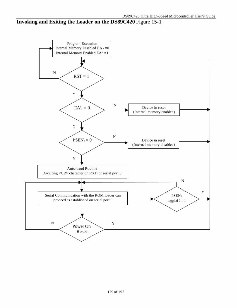
DS89C420 Ultra High-Speed Microcontroller User’s Guide
179 of 192
Invoking and Exiting the Loader on the DS89C420 Figure 15-1
Program Execution Internal Memory Disabled EA \ =0 Internal Memory Enabled EA \ =1
PSEN\ toggled 0→1
RST = 1
EA\ = 0
PSEN\ = 0
Power On Reset
Auto-baud Routine Awaiting <CR> character on RXD of serial port 0
Serial Communication with the ROM loader can proceed as established on serial port 0
Device in reset (Internal memory disabled)
Device in reset (Internal memory enabled)
N
N
N
N Y
Y
Y
Y
Y
N
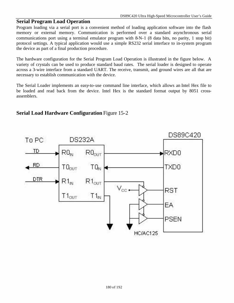
DS89C420 Ultra High-Speed Microcontroller User’s Guide
180 of 192
Serial Program Load Operation Program loading via a serial port is a convenient method of loading application software into the flash memory or external memory. Communication is performed over a standard asynchronous serial communications port using a terminal emulator program with 8-N-1 (8 data bits, no parity, 1 stop bit) protocol settings. A typical application would use a simple RS232 serial interface to in-system program the device as part of a final production procedure. The hardware configuration for the Serial Program Load Operation is illustrated in the figure below. A variety of crystals can be used to produce standard baud rates. The serial loader is designed to operate across a 3-wire interface from a standard UART. The receive, transmit, and ground wires are all that are necessary to establish communication with the device. The Serial Loader implements an easy-to-use command line interface, which allows an Intel Hex file to be loaded and read back from the device. Intel Hex is the standard format output by 8051 cross-assemblers. Serial Load Hardware Configuration Figure 15-2
DS89C420 Ultra High-Speed Microcontroller User’s Guide
181 of 192
AUTO-BAUD RATE DETECTION The Serial Bootstrap Loader can automatically detect, within certain limits, the external baud rate and configure itself to that speed. The Loader controls serial port 0 in mode 1 (asynchronous, one start bit, eight data bits, no parity, one stop bit, full duplex), using timer1 in 8-bit auto-reload mode with the serial port 0 doubler bit (PCON.7) set. For these settings, an equation to calculate possible serial loader baud rates is provided below as a function of crystal frequency and timer reload value. The table below shows baud rates generated using the equation.
)Re256(*192_
loadTimerquencyCrystalFre
BaudRateerSerialLoad−
=
** Timer Reload Values attempted by the Loader: FF, FE, FD, FC, FB, FA, F8, F6, F5, F4, F3, F0, EC, EA, E8, E6, E0, DD, D8, D4, D0, CC, C0, BA, B0, A8, A0, 98, 80, 60, 40 When communicating with a PC COM port having a standard 8250 / 16450 UART, one should attempt to match the loader baud rate and PC COM port baud rate within 3% in order to maintain a reliable communication channel. If baud rates cannot be matched exactly, it is suggested to configure the loader to the faster baud rate to avoid the possibility of overflowing the DS89C420 serial input buffer.
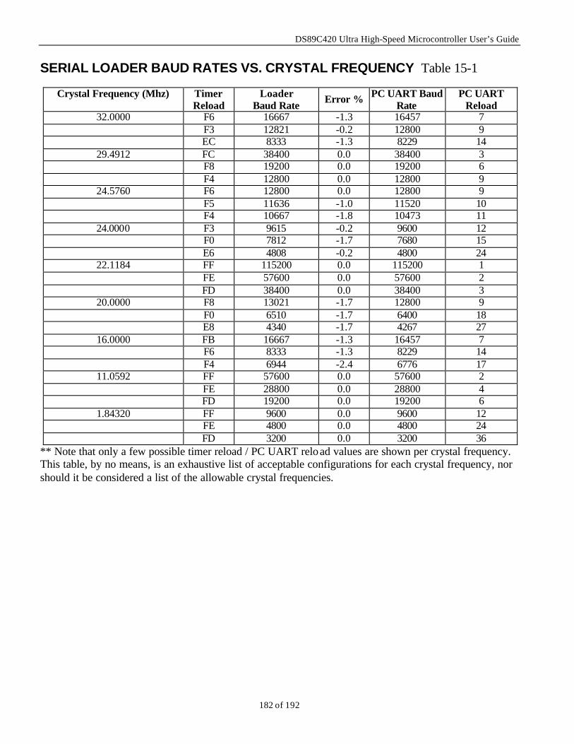
DS89C420 Ultra High-Speed Microcontroller User’s Guide
182 of 192
SERIAL LOADER BAUD RATES VS. CRYSTAL FREQUENCY Table 15-1
Crystal Frequency (Mhz) Timer Reload
Loader Baud Rate Error % PC UART Baud
Rate PC UART
Reload 32.0000 F6 16667 -1.3 16457 7
F3 12821 -0.2 12800 9 EC 8333 -1.3 8229 14
29.4912 FC 38400 0.0 38400 3 F8 19200 0.0 19200 6 F4 12800 0.0 12800 9
24.5760 F6 12800 0.0 12800 9 F5 11636 -1.0 11520 10 F4 10667 -1.8 10473 11
24.0000 F3 9615 -0.2 9600 12 F0 7812 -1.7 7680 15 E6 4808 -0.2 4800 24
22.1184 FF 115200 0.0 115200 1 FE 57600 0.0 57600 2 FD 38400 0.0 38400 3
20.0000 F8 13021 -1.7 12800 9 F0 6510 -1.7 6400 18 E8 4340 -1.7 4267 27
16.0000 FB 16667 -1.3 16457 7 F6 8333 -1.3 8229 14 F4 6944 -2.4 6776 17
11.0592 FF 57600 0.0 57600 2 FE 28800 0.0 28800 4 FD 19200 0.0 19200 6
1.84320 FF 9600 0.0 9600 12 FE 4800 0.0 4800 24 FD 3200 0.0 3200 36
** Note that only a few possible timer reload / PC UART reload values are shown per crystal frequency. This table, by no means, is an exhaustive list of acceptable configurations for each crystal frequency, nor should it be considered a list of the allowable crystal frequencies.
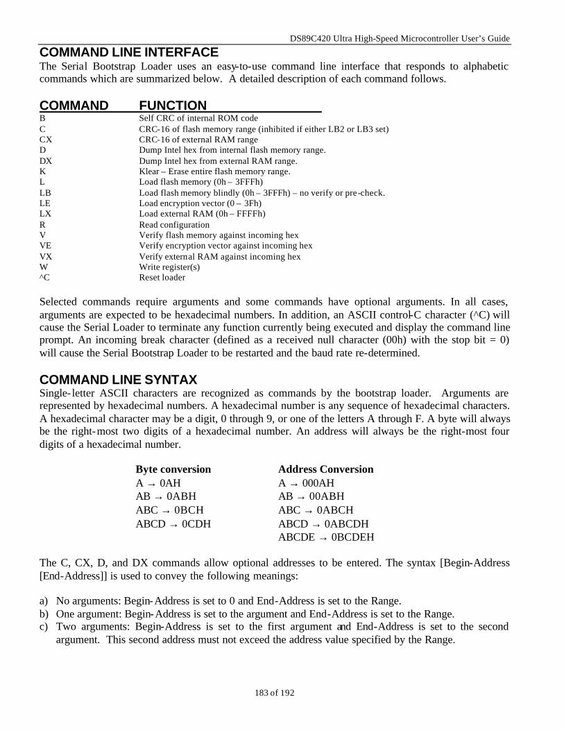
DS89C420 Ultra High-Speed Microcontroller User’s Guide
183 of 192
COMMAND LINE INTERFACE The Serial Bootstrap Loader uses an easy-to-use command line interface that responds to alphabetic commands which are summarized below. A detailed description of each command follows. COMMAND FUNCTION B Self CRC of internal ROM code C CRC-16 of flash memory range (inhibited if either LB2 or LB3 set) CX CRC-16 of external RAM range D Dump Intel hex from internal flash memory range. DX Dump Intel hex from external RAM range. K Klear – Erase entire flash memory range. L Load flash memory (0h – 3FFFh) LB Load flash memory blindly (0h – 3FFFh) – no verify or pre-check. LE Load encryption vector (0 – 3Fh) LX Load external RAM (0h – FFFFh) R Read configuration V Verify flash memory against incoming hex VE Verify encryption vector against incoming hex VX Verify external RAM against incoming hex W Write register(s) ^C Reset loader Selected commands require arguments and some commands have optional arguments. In all cases, arguments are expected to be hexadecimal numbers. In addition, an ASCII control-C character (^C) will cause the Serial Loader to terminate any function currently being executed and display the command line prompt. An incoming break character (defined as a received null character (00h) with the stop bit = 0) will cause the Serial Bootstrap Loader to be restarted and the baud rate re-determined. COMMAND LINE SYNTAX Single- letter ASCII characters are recognized as commands by the bootstrap loader. Arguments are represented by hexadecimal numbers. A hexadecimal number is any sequence of hexadecimal characters. A hexadecimal character may be a digit, 0 through 9, or one of the letters A through F. A byte will always be the right-most two digits of a hexadecimal number. An address will always be the right-most four digits of a hexadecimal number.
Byte conversion Address Conversion A → 0AH AB → 0ABH ABC → 0BCH ABCD → 0CDH
A → 000AH AB → 00ABH ABC → 0ABCH ABCD → 0ABCDH ABCDE → 0BCDEH
The C, CX, D, and DX commands allow optional addresses to be entered. The syntax [Begin-Address [End-Address]] is used to convey the following meanings: a) No arguments: Begin-Address is set to 0 and End-Address is set to the Range. b) One argument: Begin-Address is set to the argument and End-Address is set to the Range. c) Two arguments: Begin-Address is set to the first argument and End-Address is set to the second
argument. This second address must not exceed the address value specified by the Range.
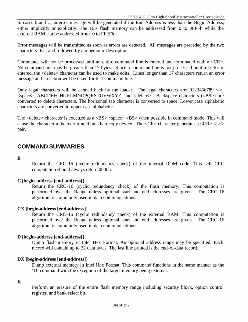
DS89C420 Ultra High-Speed Microcontroller User’s Guide
184 of 192
In cases b and c, an error message will be generated if the End Address is less than the Begin Address, either implicitly or explicitly. The 16K flash memory can be addressed from 0 to 3FFFh while the external RAM can be addressed from 0 to FFFFh. Error messages will be transmitted as soon as errors are detected. All messages are preceded by the two characters ‘E:’, and followed by a mnemonic description. Commands will not be processed until an entire command line is entered and terminated with a <CR>. No command line may be greater than 17 bytes. Since a command line is not processed until a <CR> is entered, the <delete> character can be used to make edits. Lines longer than 17 characters return an error message and no action will be taken for that command line. Only legal characters will be echoed back by the loader. The legal characters are: 0123456789 <:>, <space>, ABCDEFGHIJKLMNOPQRSTUVWXYZ, and <delete>. Backspace characters (<BS>) are converted to delete characters. The horizontal tab character is converted to space. Lower case alphabetic characters are converted to upper case alphabetic. The <delete> character is executed as a <BS> <space> <BS> when possible in command mode. This will cause the character to be overprinted on a hardcopy device. The <CR> character generates a <CR> <LF> pair.
COMMAND SUMMARIES B
Return the CRC-16 (cyclic redundancy check) of the internal ROM code. This self CRC computation should always return 0000h.
C [begin-address [end-address]]
Return the CRC-16 (cyclic redundancy check) of the flash memory. This computation is performed over the Range unless optional start and end addresses are given. The CRC-16 algorithm is commonly used in data communications.
CX [begin-address [end-address]]
Return the CRC-16 (cyclic redundancy check) of the external RAM. This computation is performed over the Range unless optional start and end addresses are given. The CRC-16 algorithm is commonly used in data communications
D [begin-address [end-address]]
Dump flash memory in Intel Hex Format. An optional address range may be specified. Each record will contain up to 32 data bytes. The last line printed is the end-of-data record.
DX [begin-address [end-address]]
Dump external memory in Intel Hex Format. This command functions in the same manner as the ‘D’ command with the exception of the target memory being external.
K
Perform an erasure of the entire flash memory range including security block, option control register, and bank select bit.
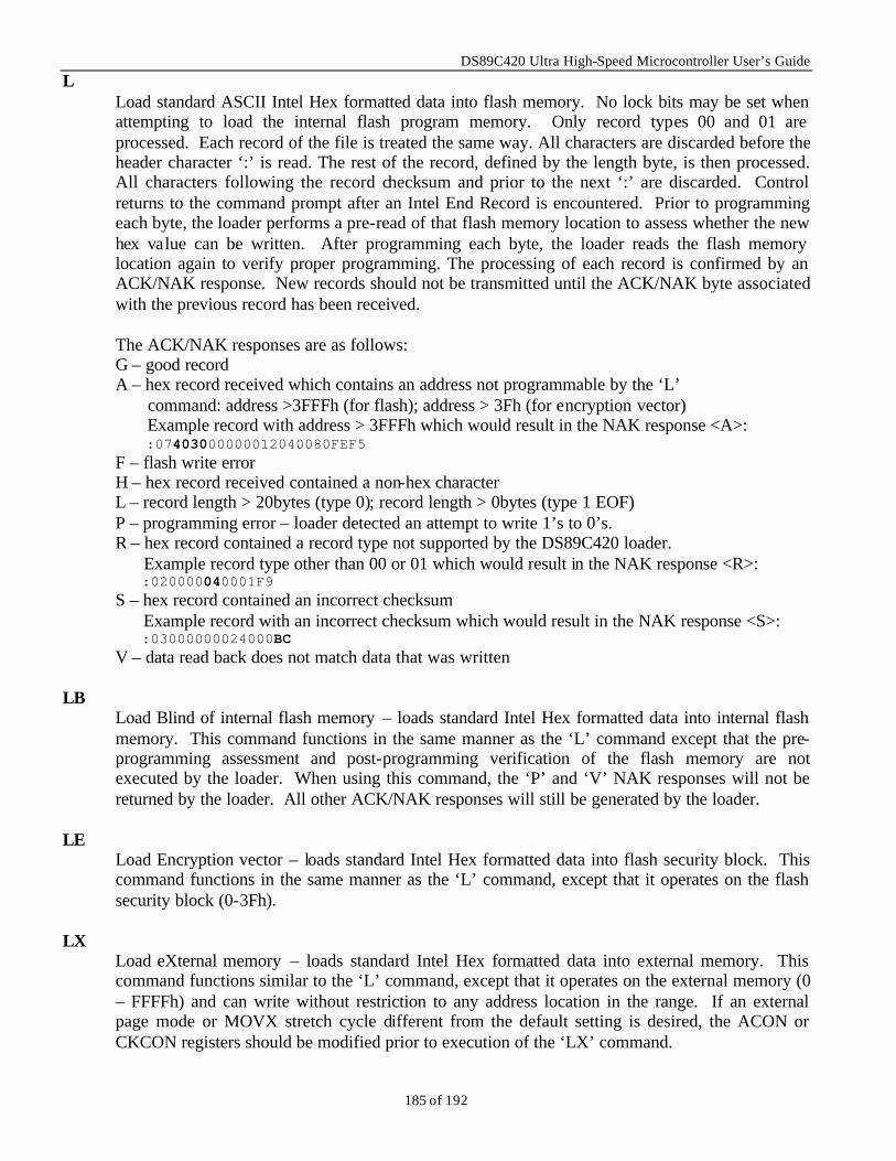
DS89C420 Ultra High-Speed Microcontroller User’s Guide
185 of 192
L Load standard ASCII Intel Hex formatted data into flash memory. No lock bits may be set when attempting to load the internal flash program memory. Only record types 00 and 01 are processed. Each record of the file is treated the same way. All characters are discarded before the header character ‘:’ is read. The rest of the record, defined by the length byte, is then processed. All characters following the record checksum and prior to the next ‘:’ are discarded. Control returns to the command prompt after an Intel End Record is encountered. Prior to programming each byte, the loader performs a pre-read of that flash memory location to assess whether the new hex value can be written. After programming each byte, the loader reads the flash memory location again to verify proper programming. The processing of each record is confirmed by an ACK/NAK response. New records should not be transmitted until the ACK/NAK byte associated with the previous record has been received.
The ACK/NAK responses are as follows:
G – good record A – hex record received which contains an address not programmable by the ‘L’ command: address >3FFFh (for flash); address > 3Fh (for encryption vector) Example record with address > 3FFFh which would result in the NAK response <A>: :07403000000012040080FEF5
F – flash write error H – hex record received contained a non-hex character L – record length > 20bytes (type 0); record length > 0bytes (type 1 EOF) P – programming error – loader detected an attempt to write 1’s to 0’s. R – hex record contained a record type not supported by the DS89C420 loader. Example record type other than 00 or 01 which would result in the NAK response <R>: :020000040001F9 S – hex record contained an incorrect checksum Example record with an incorrect checksum which would result in the NAK response <S>: :03000000024000BC V – data read back does not match data that was written LB
Load Blind of internal flash memory – loads standard Intel Hex formatted data into internal flash memory. This command functions in the same manner as the ‘L’ command except that the pre-programming assessment and post-programming verification of the flash memory are not executed by the loader. When using this command, the ‘P’ and ‘V’ NAK responses will not be returned by the loader. All other ACK/NAK responses will still be generated by the loader.
LE
Load Encryption vector – loads standard Intel Hex formatted data into flash security block. This command functions in the same manner as the ‘L’ command, except that it operates on the flash security block (0-3Fh).
LX Load eXternal memory – loads standard Intel Hex formatted data into external memory. This command functions similar to the ‘L’ command, except that it operates on the external memory (0 – FFFFh) and can write without restriction to any address location in the range. If an external page mode or MOVX stretch cycle different from the default setting is desired, the ACON or CKCON registers should be modified prior to execution of the ‘LX’ command.
DS89C420 Ultra High-Speed Microcontroller User’s Guide
186 of 192
R
Read – Displays the values of the Lock bits, Option Control Register, Address Control Register, Clock Control Register, Power Management Register, Ports 0, 1, 2, 3 and the Flash Control Register in the following format: LB:XX OCR:XX ACON:XX CKCON:XX PMR:XX P0:XX P1:XX P2:XX P3:XX FCNTL:XX
V
Verify current contents of flash memory versus the received Intel hex. This command operates similar to the Load command, except that it does not write to the flash memory; it simply compares the data byte(s) in the flash memory to the byte(s) in the data stream. The same ACK/NAK response scheme is used during verify operations as is used for load operations.
VE
Verify Encryption vector – verifies current contents of the flash security block versus the received Intel hex. This command works in the same manner as the ‘V’ command, but operates on the flash security block (0-3Fh).
VX
Verify eXternal memory – verifies current contents of external memory versus the received Intel hex. This command works in the same manner as the ‘V’ command, but operates on external memory (0-FFFFh).
W [LB | OCR | ACON | CKCON | PMR | P0 | P1 | P2 | P3] byte
Writes byte to the requested register. Valid entries for LB are 1 (enable LB1), 3 (enable LB1,LB2) and 7 (enable LB1,LB2,LB3). ACON register writes will modify only bits 7,6,5. CKCON register writes will modify only bits 2,1,0. PMR register writes will modify only bit 0. P3 register writes will modify only P3.7-P3.2 (P3.1 and P3.0 will not be altered).
^C
Interrupt whatever is going on, clear all the buffers, put up a prompt and wait for the next command. Anything in the type-ahead buffer is removed. All output is stopped.
DS89C420 Ultra High-Speed Microcontroller User’s Guide
187 of 192
ERROR MESSAGES E:ARGREQ An argument or arguments is required for this command. E:BADCMD An invalid command letter was entered. E:BADREG This message is printed if a register other than OCR, ACON, CKCON, PMR, P0, P1, P2, or P3 is used as the argument for the W command. E:BADVAL The requested value cannot be programmed into the OCR register because it contains 1’s in bit position(s) where 0’s have already been programmed. E:EXTARG Extra data was encountered on the command line when it wasn’t needed. Reenter the command. E:ILLOPT The optional parameters given were in error. If the start address is greater than the end address, either implicitly or explicitly, then an error is printed. The range bit implicitly determines the maximum range. E:LOCK BITS ENABLED The requested operation cannot be performed because due to the current lock bit settings. E:LOCK BITS ALREADY SET The requested lock bit setting cannot be programmed because a higher order lock bit has already been programmed. E:NOTHEX A non-hexadecimal character was found when expecting a hexadecimal character. E:VALUE MUST BE 1,3 OR 7 A value other than 1,3, or 7 was entered when trying to write the lock bits.
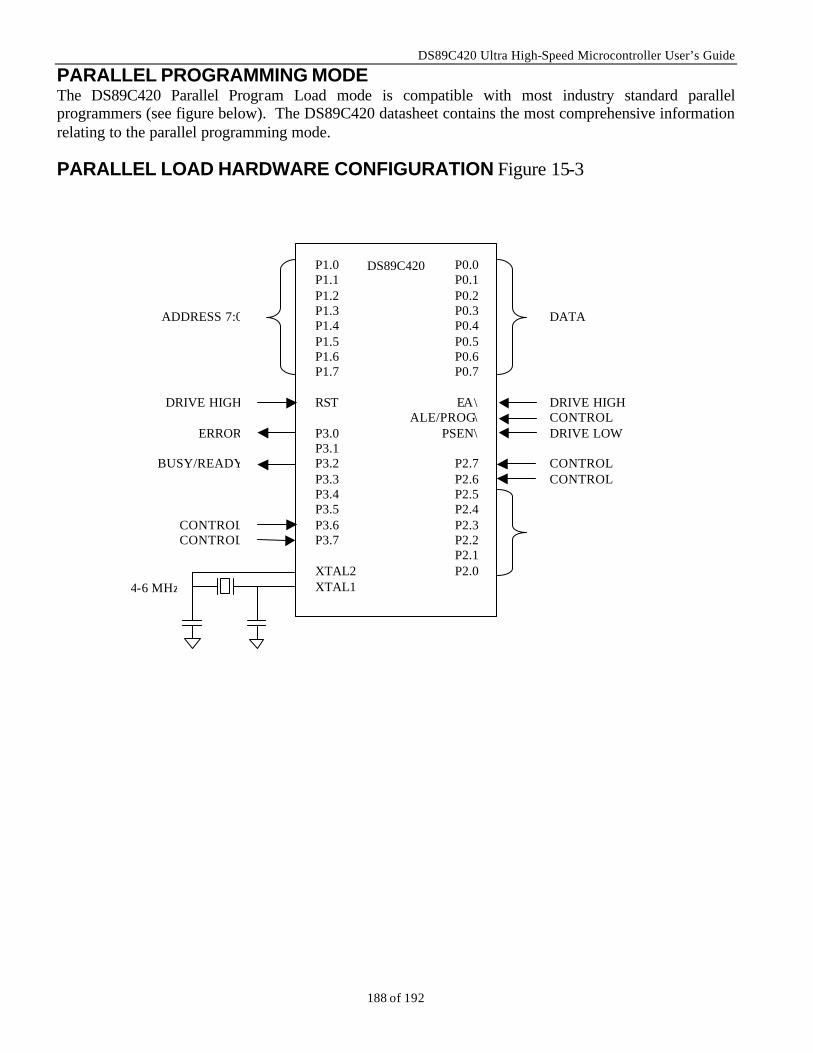
DS89C420 Ultra High-Speed Microcontroller User’s Guide
188 of 192
PARALLEL PROGRAMMING MODE The DS89C420 Parallel Program Load mode is compatible with most industry standard parallel programmers (see figure below). The DS89C420 datasheet contains the most comprehensive information relating to the parallel programming mode. PARALLEL LOAD HARDWARE CONFIGURATION Figure 15-3
P1.0 P1.1 P1.2 P1.3 P1.4 P1.5 P1.6 P1.7 RST P3.0 P3.1 P3.2 P3.3 P3.4 P3.5 P3.6 P3.7 XTAL2 XTAL1
P0.0P0.1P0.2P0.3P0.4P0.5P0.6P0.7
EA\ALE/PROG\
PSEN\
P2.7P2.6P2.5P2.4P2.3P2.2P2.1P2.0
DS89C420
DATA
DRIVE HIGH CONTROL DRIVE LOW CONTROL CONTROL
ADDRESS 7:0
DRIVE HIGH
ERROR
BUSY/READY
CONTROLCONTROL
4-6 MHz

DS89C420 Ultra High-Speed Microcontroller User’s Guide
189 of 192
USER CODE IN-APPLICATION PROGRAMMING MODE The DS89C420 datasheet contains the most comprehensive information relating to the in-application programming mode. Additional supporting information can be found in the SFR definitions of FCNTL (D5h) and FDATA (F6h) of this user guide.
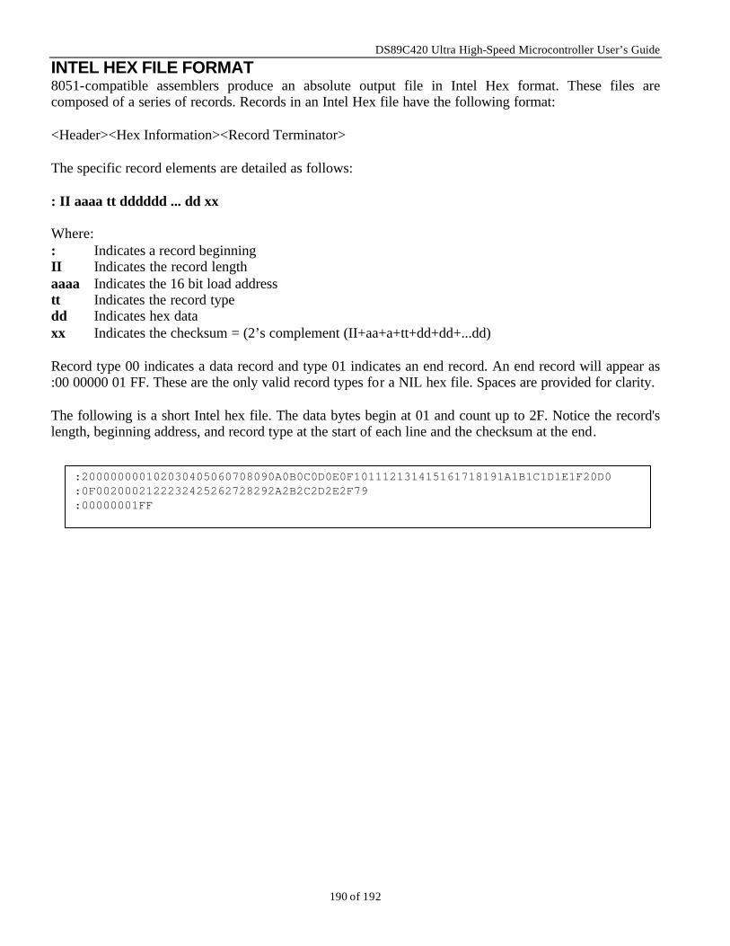
DS89C420 Ultra High-Speed Microcontroller User’s Guide
190 of 192
INTEL HEX FILE FORMAT 8051-compatible assemblers produce an absolute output file in Intel Hex format. These files are composed of a series of records. Records in an Intel Hex file have the following format: <Header><Hex Information><Record Terminator> The specific record elements are detailed as follows: : II aaaa tt dddddd ... dd xx Where: : Indicates a record beginning II Indicates the record length aaaa Indicates the 16 bit load address tt Indicates the record type dd Indicates hex data xx Indicates the checksum = (2’s complement (II+aa+a+tt+dd+dd+...dd) Record type 00 indicates a data record and type 01 indicates an end record. An end record will appear as :00 00000 01 FF. These are the only valid record types for a NIL hex file. Spaces are provided for clarity. The following is a short Intel hex file. The data bytes begin at 01 and count up to 2F. Notice the record's length, beginning address, and record type at the start of each line and the checksum at the end.
:200000000102030405060708090A0B0C0D0E0F101112131415161718191A1B1C1D1E1F20D0 :0F0020002122232425262728292A2B2C2D2E2F79 :00000001FF

DS89C420 Ultra High-Speed Microcontroller User’s Guide
191 of 192
REVISION HISTORY January 24, 2001 Original Issue