dallas semiconductor secure microcontroller user's guide
TRANSCRIPT
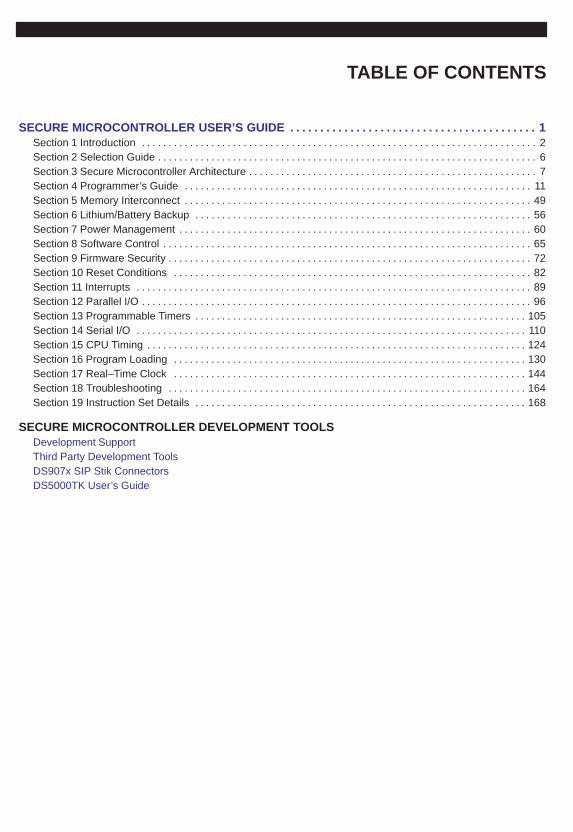
TABLE OF CONTENTS
i
SECURE MICROCONTROLLER USER’S GUIDE 1. . . . . . . . . . . . . . . . . . . . . . . . . . . . . . . . . . . . . . . . . Section 1 Introduction 2. . . . . . . . . . . . . . . . . . . . . . . . . . . . . . . . . . . . . . . . . . . . . . . . . . . . . . . . . . . . . . . . . . . . . . . . . . Section 2 Selection Guide 6. . . . . . . . . . . . . . . . . . . . . . . . . . . . . . . . . . . . . . . . . . . . . . . . . . . . . . . . . . . . . . . . . . . . . . . Section 3 Secure Microcontroller Architecture 7. . . . . . . . . . . . . . . . . . . . . . . . . . . . . . . . . . . . . . . . . . . . . . . . . . . . . . Section 4 Programmer’s Guide 11. . . . . . . . . . . . . . . . . . . . . . . . . . . . . . . . . . . . . . . . . . . . . . . . . . . . . . . . . . . . . . . . . Section 5 Memory Interconnect 49. . . . . . . . . . . . . . . . . . . . . . . . . . . . . . . . . . . . . . . . . . . . . . . . . . . . . . . . . . . . . . . . . Section 6 Lithium/Battery Backup 56. . . . . . . . . . . . . . . . . . . . . . . . . . . . . . . . . . . . . . . . . . . . . . . . . . . . . . . . . . . . . . . Section 7 Power Management 60. . . . . . . . . . . . . . . . . . . . . . . . . . . . . . . . . . . . . . . . . . . . . . . . . . . . . . . . . . . . . . . . . . Section 8 Software Control 65. . . . . . . . . . . . . . . . . . . . . . . . . . . . . . . . . . . . . . . . . . . . . . . . . . . . . . . . . . . . . . . . . . . . . Section 9 Firmware Security 72. . . . . . . . . . . . . . . . . . . . . . . . . . . . . . . . . . . . . . . . . . . . . . . . . . . . . . . . . . . . . . . . . . . . Section 10 Reset Conditions 82. . . . . . . . . . . . . . . . . . . . . . . . . . . . . . . . . . . . . . . . . . . . . . . . . . . . . . . . . . . . . . . . . . . Section 11 Interrupts 89. . . . . . . . . . . . . . . . . . . . . . . . . . . . . . . . . . . . . . . . . . . . . . . . . . . . . . . . . . . . . . . . . . . . . . . . . . Section 12 Parallel I/O 96. . . . . . . . . . . . . . . . . . . . . . . . . . . . . . . . . . . . . . . . . . . . . . . . . . . . . . . . . . . . . . . . . . . . . . . . . Section 13 Programmable Timers 105. . . . . . . . . . . . . . . . . . . . . . . . . . . . . . . . . . . . . . . . . . . . . . . . . . . . . . . . . . . . . . Section 14 Serial I/O 110. . . . . . . . . . . . . . . . . . . . . . . . . . . . . . . . . . . . . . . . . . . . . . . . . . . . . . . . . . . . . . . . . . . . . . . . . Section 15 CPU Timing 124. . . . . . . . . . . . . . . . . . . . . . . . . . . . . . . . . . . . . . . . . . . . . . . . . . . . . . . . . . . . . . . . . . . . . . . Section 16 Program Loading 130. . . . . . . . . . . . . . . . . . . . . . . . . . . . . . . . . . . . . . . . . . . . . . . . . . . . . . . . . . . . . . . . . . Section 17 Real–Time Clock 144. . . . . . . . . . . . . . . . . . . . . . . . . . . . . . . . . . . . . . . . . . . . . . . . . . . . . . . . . . . . . . . . . . Section 18 Troubleshooting 164. . . . . . . . . . . . . . . . . . . . . . . . . . . . . . . . . . . . . . . . . . . . . . . . . . . . . . . . . . . . . . . . . . . Section 19 Instruction Set Details 168. . . . . . . . . . . . . . . . . . . . . . . . . . . . . . . . . . . . . . . . . . . . . . . . . . . . . . . . . . . . . .
SECURE MICROCONTROLLER DEVELOPMENT TOOLSDevelopment SupportThird Party Development ToolsDS907x SIP Stik ConnectorsDS5000TK User’s Guide
USER’S GUIDE
050396 1/173
2
SECTION 1: INTRODUCTIONThe Secure Microcontroller family is a line of8051–compatible devices that utilize nonvolatile RAM(NV RAM) rather than ROM for program storage. Theuse of NV RAM allows the design of a “soft” microcon-troller which provides a number of unique features toembedded system designers. Foremost among these isthe enhanced security features that are employed bythe Secure Microcontroller Family to protect the userapplication software against piracy and tampering.These devices offer varying degrees of security, rangingfrom simple access prevention to a full encryption ofprogram and data memory of the device. Attempts togain access to protected information will result in theself–destruction of all data. The Secure Microcontrollerfamily is the heart of a wide range of security–critical ap-plications such as electronic banking, commercialtransactions, and pay TV access control, or any situa-tion which requires the protection of proprietary soft-ware and algorithms.
The Secure Microcontroller family is divided betweenchips and modules. The chips are monolithic micropro-cessors that connect to a standard SRAM and lithiumbattery. The modules combine the microprocessor withthe SRAM and lithium battery in a preassembled, pre-tested module. Depending on the specific configuration,modules are available in either 40–pin encapsulatedDIP or SIMM module format.
In addition to NV RAM, Dallas Semiconductor micro-controllers offer a number of peripherals that simplifyand reduce the cost of embedded systems. Althoughthe specific features of each chip or module vary, all de-vices offer the following basic feature set:
• 100% code–compatible with 8051
• Directly addresses 64KB program/64KB datamemory
• Nonvolatile memory control circuitry
• 10–year data retention in the absence of power
• In–system reprogramming via serial port
• 128 bytes fast access scratchpad RAM
• Two 16–bit general purpose timer/counters
• One UART
• Five interrupts with two external
• Dedicated memory bus, preserving four 8–bit portsfor general purpose I/O
• Power–Fail Reset
• Early Warning Power Fail Interrupt
• Watchdog Timer
SOFTWARE SECURITYOne of the most important features of the Secure Micro-controller family is firmware/memory security. The de-vices were specifically designed to offer an unprece-dented level of protection to the user applicationsoftware, preventing unauthorized copying of firmwareand denying access to critical data values. The use ofRAM rather than the traditional ROM or EPROM for pro-gram storage increases the security, since tamperingwith the system will result in the loss of the RAM con-tents. Additional features such as real–time high–speedmemory encryption, generation of dummy addresseson the bus, and internal storage of vector RAM in-creases the security of a Secure Microcontroller/Micro-processor–based system.
The DS5002FP Secure Microprocessor Chip andDS2252T Secure Microcontroller Module offer the high-est level of security, with permanently enabled memoryencryption, a 64–bit random encryption key, and a self–destruct input for tamper protection. The DS5000FPSoft Microprocessor Chip and DS5000(T) andDS2250(T) Soft Microcontroller Modules offer lesser,but still substantial, protection with optional data encryp-tion and a 48–bit encryption key.
SEPARATE ADDRESS/DATA BUSSoft Microprocessor chips provide a non–multiplexedaddress/data bus that interfaces to memory without in-terfering with I/O ports. This Byte–wide bus connects di-rectly to standard CMOS SRAM in 8K x 8, 32K x 8, or128K x 8 densities with no glue logic. Note that this is inaddition to the standard 8051 port 0 and 2 multiplexedbus. In module form, the Byte–wide bus is already con-nected directly to on–board SRAM, so the memory ac-cess becomes transparent and the I/O ports free for ap-plication use. The extra memory bus also allows for atime–of–day function to be included, and all Soft Micro-controller modules are available with built in real–timeclocks. The same clock devices are individually avail-able when building a system from chips. Battery backupand decoding are automatically handled by the micro-processor.
USER’S GUIDE
050396 2/173
3
LARGE NONVOLATILE MEMORYSoft Microprocessor chips provide nonvolatile memorycontrol for standard CMOS SRAM. Modules combinethe microprocessor chip with memory and lithium back-up. This includes conditionally write protected chip en-ables and a power supply output that switches between+5V and battery backup. The chip enables are decodedautomatically based on user selectable memory sizesand partitioning. Partitioning defines the portion ofmemory used for program and data segments. Areasthat are designated program are always write protectedand are treated as ROM. Data areas are write protectedonly when power is out of tolerance. A large nonvolatilememory is useful for data logging and as flexible pro-gram storage. Memory will be retained for over 10 yearsat room temperature in the absence of power by ultralow–leakage lithium backed circuits.
IN–SYSTEM LOADINGThe in–system programming capability lets the user up-date program code at any time. This program loading issupervised by a built–in ROM–based bootstrap loader.The ROM loader becomes transparent once programloading is complete. All devices allow program loadingvia the serial port. Data memory can also be retrievedusing this loader function. Selected versions provide
other parallel loading protocols as well. In–system load-ing allows a system to be configured during final systemtest. A user can load custom software, diagnostic rou-tines, or calibration constants. If something changes ornew features arise, the system can then be repro-grammed while in the field.
HIGH RELIABILITY OPERATIONSecure Microcontroller devices are designed for unsu-pervised operation in remote locations. Special fea-tures prevent a system from running out of control dur-ing transient events. These include a reset when poweris out of tolerance; an early warning power–fail interruptthat allows software to save critical data; and a watch-dog to reset the micro if it gets lost. Also, nonvolatilememory allows software to save the operating state so atask can be resumed when power returns to normal.
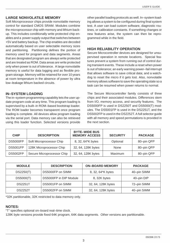
The Secure Microcontroller family consists of threechips and their associated modules. Differences stemfrom I/O, memory access, and security features. TheDS5000FP is used in DS2250T and DS5000(T) mod-ules. The DS5001FP is used in the DS2251T, and theDS5002FP is used in the DS2252T. A full selector guidewith all memory and speed permutations is provided inthe next section.
CHIP DESCRIPTIONBYTE–WIDE BUS
MEMORY ACCESS SECURITY PACKAGE
DS5000FP Soft Microprocessor Chip 8, 32, 64*K bytes Optional 80–pin QFP
DS5001FP 128K Microprocessor Chip 32, 64, 128K bytes None 80–pin QFP
DS5002FP Secure Microprocessor Chip 32, 64, 128K bytes Maximum 80–pin QFP
MODULE DESCRIPTION ON–BOARD MEMORY PACKAGE
DS2250(T) DS5000FP on SIMM 8, 32, 64*K bytes 40–pin SIMM
DS5000(T) DS5000FP in DIP Module 8, 32K bytes 40–pin DIP
DS2251T DS5001FP on SIMM 32, 64, 128K bytes 72–pin SIMM
DS2252T DS5002FP on SIMM 32, 64, 128K bytes 40–pin SIMM
*32K partitionable, 32K restricted to data memory only.
NOTES:“T” specifies optional on–board real–time clock.128K byte versions provide fixed 64K program, 64K data segments. Other versions are partitionable.
USER’S GUIDE
050396 3/173
4
PRODUCT DESCRIPTIONAll devices listed below have the standard 8051 familyfeature set listed once here for convenience, but not re-peated for each device.
• 8051–compatible instruction set
• Addresses 64K program and 64K data memory
• Four 8–bit pseudo–bidirectional I/O ports
• 128 bytes scratchpad RAM
• Two 16–bit timer/counters
• One UART
• Five Interrupts with two external
DS5000FP Soft Microprocessor ChipThe DS5000FP is the original Soft Microprocessor chip.It adds the following features to the 8051 set :
• Non–multiplexed Byte–wide address/data bus formemory access.
• Nonvolatile Control for 8K x 8 or 32K x 8 SRAMs
• Partitions one SRAM into program and data areas,and write protects the program segment
• Decodes memory for up to two 32K x 8 SRAMs (#2is data memory only)
• Power–fail Reset, and Interrupt
• Precision Watchdog Timer
• ROM based Serial Bootstrap Loader
• Optional security features
– Memory encryption in real–time– 48–bit user selected encryption key– Security lock destroys memory if unlocked– Vector RAM hides 48 bytes on–chip– Dummy operations on the memory bus
DS5000(T) Soft Microcontroller ModuleThe DS5000 incorporates the DS5000FP chip in a40–pin module with an 8051 footprint and pinout.
• Familiar 40–pin DIP package
• Built–in NV RAM of 8K x 8 or 32K x 8
• I/O ports not disturbed by on–board memory access
• 10–year data retention and clock operation in theabsence of power
• Partitions memory into program and data areas,write protects the program segment
• Power–fail Reset and Interrupt
• Precision Watchdog Timer
• ROM based Serial Bootstrap Loader
• Optional memory security
• Optional built–in real time clock (battery backed)
DS2250(T) Soft Microcontroller ModuleThe DS2250(T) incorporates the DS5000FP chip on a40–pin SIMM module. It has the identical feature set asthe DS5000(T), but is in a different form–factor. Thispackage change allows up to 64K bytes NV RAMinstead of 32K bytes. Note that as mentioned above, thesecond 32K is restricted to data memory. Like theDS5000(T), this module guarantees better than10–year data retention at room temperature.
DS5001FP 128K Soft Microprocessor ChipThe DS5001FP provides the base feature set of theDS5000FP with the following extras:
• Accesses up to 128K bytes on the Byte–wide bus.
• Decodes memory for 32K x 8 or 128K x 8 SRAMs.
• Four additional decoded peripheral chip enables
• CRC hardware for checking memory validity
• Optionally emulates an 8042 style slave interface
• Bandgap reference for more accurate power moni-tor
Note: The DS5001FP has no memory encryptionfeature.
USER’S GUIDE
050396 4/173
5
DS2251T 128K Soft Microcontroller ModuleThe DS2251T is a SIMM based on the DS5001. It pro-vides up to 128K bytes of on–board NV RAM and hasthe Byte–wide bus available at the connector. This isused with the decoded peripheral enables for memorymapped peripherals such as a UART or A/D converter.The real–time clock is a parallel access type with inter-rupt capability. Like the older versions, the DS2251Tprovides 10–year data retention, even in the largestmemory configuration.
DS5002FP Secure Microprocessor ChipThe DS5002FP is a highly secure version of theDS5001FP. It provides the operating features of theDS5001FP, with the following enhancements to theDS5000 security features.
• Security is active at all times
• Improved memory encryption using a 64–bit en-cryption key
• Automatic random generation of encryption keys
• Self–destruct input for tamper protection
• Optional top–coating prevents microprobe(DS5002FPM)
DS2252T Secure Microcontroller ModuleThe DS2252T incorporates the DS5002FP on a 40–pinSIMM. This includes from 32K bytes to 128K bytes ofsecure memory with a real time clock. The memory ishighly secure from tampering and from competitors.Like other products in the family, the D2252T has a dataretention period of over 10 years at room temperature.
USER’S GUIDE
050396 5/173
6
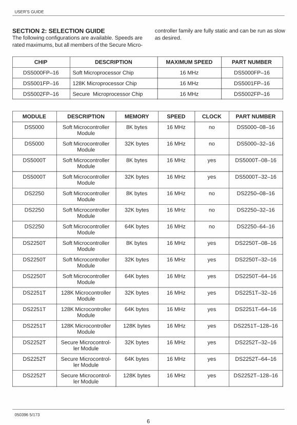
SECTION 2: SELECTION GUIDEThe following configurations are available. Speeds arerated maximums, but all members of the Secure Micro-
controller family are fully static and can be run as slowas desired.
CHIP DESCRIPTION MAXIMUM SPEED PART NUMBER
DS5000FP–16 Soft Microprocessor Chip 16 MHz DS5000FP–16
DS5001FP–16 128K Microprocessor Chip 16 MHz DS5001FP–16
DS5002FP–16 Secure Microprocessor Chip 16 MHz DS5002FP–16
MODULE DESCRIPTION MEMORY SPEED CLOCK PART NUMBER
DS5000 Soft MicrocontrollerModule
8K bytes 16 MHz no DS5000–08–16
DS5000 Soft MicrocontrollerModule
32K bytes 16 MHz no DS5000–32–16
DS5000T Soft MicrocontrollerModule
8K bytes 16 MHz yes DS5000T–08–16
DS5000T Soft MicrocontrollerModule
32K bytes 16 MHz yes DS5000T–32–16
DS2250 Soft MicrocontrollerModule
8K bytes 16 MHz no DS2250–08–16
DS2250 Soft MicrocontrollerModule
32K bytes 16 MHz no DS2250–32–16
DS2250 Soft MicrocontrollerModule
64K bytes 16 MHz no DS2250–64–16
DS2250T Soft MicrocontrollerModule
8K bytes 16 MHz yes DS2250T–08–16
DS2250T Soft MicrocontrollerModule
32K bytes 16 MHz yes DS2250T–32–16
DS2250T Soft MicrocontrollerModule
64K bytes 16 MHz yes DS2250T–64–16
DS2251T 128K MicrocontrollerModule
32K bytes 16 MHz yes DS2251T–32–16
DS2251T 128K MicrocontrollerModule
64K bytes 16 MHz yes DS2251T–64–16
DS2251T 128K MicrocontrollerModule
128K bytes 16 MHz yes DS2251T–128–16
DS2252T Secure Microcontrol-ler Module
32K bytes 16 MHz yes DS2252T–32–16
DS2252T Secure Microcontrol-ler Module
64K bytes 16 MHz yes DS2252T–64–16
DS2252T Secure Microcontrol-ler Module
128K bytes 16 MHz yes DS2252T–128–16

USER’S GUIDE
050396 6/173
7
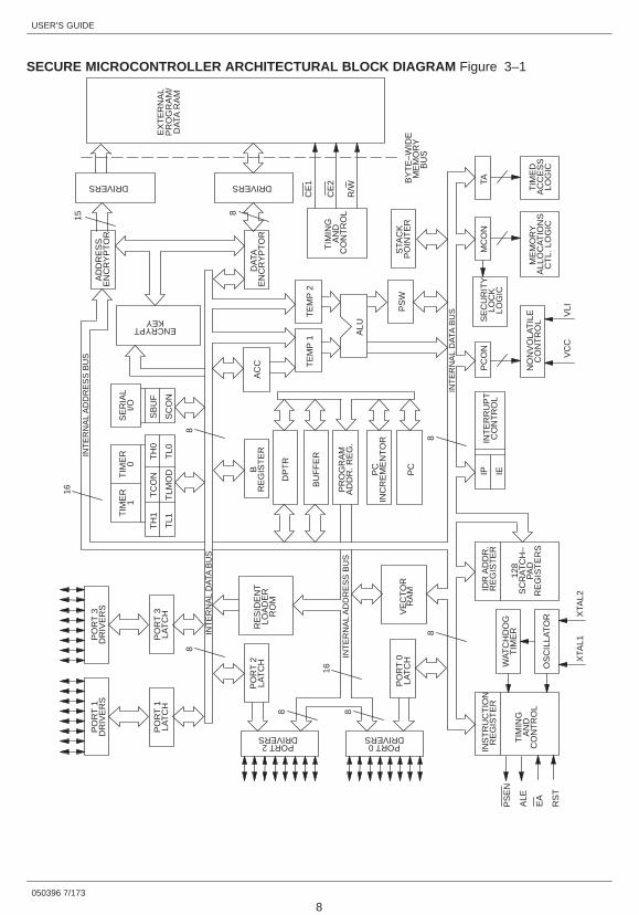
SECTION 3: SECURE MICROCONTROLLERARCHITECTUREIntroductionThe Secure Microcontroller family is based on an 8051compatible core with a memory interface and I/O logicbuild around it. Many functions are identical to standard8051s and are documented here for completeness. Ingeneral, most architecture features apply to all mem-bers of the Secure Microcontroller family. When there isa difference between versions, this will be mentioned. Ablock diagram of the microcontroller core is shown inFigure 3–1 below.
Bus OrganizationThere are four major busses in the Secure Microproces-sor: the Internal Data Bus, the Internal Address Bus, theByte–wide Memory Bus, and the Expanded Bus. All ad-dresses and data which are transferred during programexecution are passed on the Internal Address and DataBusses. User Program and Data Memory is always ac-cessed from either the byte–wide Program/Data RAMor from external memory located on the Expanded Bus.
The Byte–wide Memory Bus is used for access to Pro-gram/Data RAM in the same fashion as an 8051 Familydevice would access internal ROM or EPROM memory.This bus can be used in place of the Expanded Bus,freeing Port 2 and Port 0 pins for general I/O use.
CPU RegistersAll of the CPU registers are mapped as Special FunctionRegisters (SFR’s) and are identical in number and func-tion to those present within the 8051. These registersare described briefly below:
AccumulatorThe Accumulator (A) is used as either a source or des-tination register in all arithmetic instructions. It may alsobe used in most other types of instructions.
Stack PointerThe Stack Pointer (SP) is an 8–bit register which is usedto mark the location of the last byte of data stored in thestack. The stack itself may be located anywhere in theon–chip 128–byte Scratchpad register area. The StackPointer pre-increments during a stack push and post-decrements during a stack pop.
B RegisterThe major function of the B register is as a source anddestination register during multiply and divide instruc-tions. It may also be used as a scratchpad register.
Program Status WordThe Program Status Word (PSW) contains status flagsthat are set according to the results of a previouslyexecuted instruction. In addition, the PSW contains reg-ister bank select bits.
Data PointerThe Data Pointer (DPTR) is used to access DataMemory that may be mapped into Byte–wide Data RAMor onto external memory devices on the Expanded Bus.It is accessed by the user’s program as either two 8–bitSpecial Function registers or as a 16–bit register withcertain instructions.
Scratchpad RegistersScratchpad registers are 128 registers where data maybe stored directly. They are addressed from 00H to 7FHand may be accessed by a MOV instruction. Included inthe scratchpad area are four 8–byte banks of workingregisters. These registers are not part of the datamemory map.
Serial I/OThe on–chip serial I/O port is comprised of a receivedata buffer, a transmit data buffer, and a control register.Both the receive data buffer and the transmit data bufferare accessed in a single location (SBUF) in the SpecialFunction Register map. The control register (SCON) isaccessed in an separate location. When the serial I/Ofunction is enabled, two external I/O pins (P3.0, P3.1)are re–assigned in hardware to serve the transmit andreceive data functions.
Programmable TimersTwo 16–bit programmable timers are included that canperform various timing and counting functions. A total offour registers (TH1, TL1, TH0, and TL0) access the up-per and lower halves of each of the two timer/counters.A single control register (TCON) is used to select thevarious operating modes of the two timers. Two externalI/O pins (P3.4, P3.5) may be programmed to serve asexternal counter inputs, one pin for each of the two tim-er/counters.
USER’S GUIDE
050396 7/173
8
SECURE MICROCONTROLLER ARCHITECTURAL BLOCK DIAGRAM Figure 3–115
8
CE
1
CE
2
R/W
AD
DR
ES
SE
NC
RY
PT
OR
DA
TAE
NC
RY
PT
OR
TIM
ING
A
ND
CO
NT
RO
L
TAM
CO
NS
EC
UR
ITY
LOC
KLO
GIC
PC
ON
TIM
ED
AC
CE
SS
LOG
IC
ME
MO
RY
ALL
OC
AT
ION
SC
TL.
LO
GIC
NO
NV
OLA
TIL
EC
ON
TR
OL
INT
ER
RU
PT
CO
NT
RO
LIP IE
INT
ER
NA
L D
ATA
BU
S
STA
CK
PO
INT
ER
PS
W
IDR
AD
DR
.R
EG
IST
ER
128
SC
RA
TC
H–
PA
DR
EG
IST
ER
S
WA
TC
HD
OG
TIM
ER
OS
CIL
LAT
OR
INS
TR
UC
TIO
NR
EG
IST
ER
TIM
ING
AN
DC
ON
TR
OL
VC
CV
LI
XTA
L1X
TAL2
VE
CT
OR
RA
MP
OR
T 0
LAT
CH
TE
MP
1T
EM
P 2
AC
C
ALU
BR
EG
IST
ER
DP
TR
BU
FF
ER
PR
OG
RA
MA
DD
R. R
EG
.
PC
INC
RE
ME
NT
OR
PC
RE
SID
EN
TLO
AD
ER
RO
M
PO
RT
2LA
TC
H
INT
ER
NA
L A
DD
RE
SS
BU
S
INT
ER
NA
L D
ATA
BU
S
DRIVERS DRIVERS
PORT 2DRIVERS
PORT 0DRIVERS
ENCRYPTKEY
88
88
88
16
SE
RIA
LI/O
TIM
ER
0T
IME
R1
TH
1
TL1
TC
ON
TLM
OD
TH
0
TL0
SB
UF
SC
ON
PO
RT
3D
RIV
ER
SP
OR
T 1
DR
IVE
RS
PO
RT
1LA
TC
HP
OR
T 3
LAT
CH
16
INT
ER
NA
L A
DD
RE
SS
BU
S
BY
TE
–WID
EM
EM
OR
YB
US
PS
EN
ALE
EA
RS
T
EX
TE
RN
AL
PR
OG
RA
M/
DA
TA R
AM
USER’S GUIDE
050396 8/173
9
Parallel I/OFour SFR’s provide access for the four parallel I/O portlatches. These I/O ports are denoted as P0, P1, P2, andP3. A total of 32 bits of parallel I/O is available throughthese I/O ports. However, up to 16 bits are sacrificedwhen the Expanded Bus mode is used to interface to ex-ternal memory and up to six bits may be sacrificed if anyexternal interrupt inputs, timer counter inputs, or serialI/O functions are used. When using the Byte–wide bus,ports are not affected.
Program/Data RAM InterfaceSecure Microcontrollers provide a non–multiplexedByte–wide bus that connects to external SRAM. Theyalso make this RAM nonvolatile, decode memory ac-cess for it, and write–protect portions designated as pro-gram memory. The Byte–wide bus consists of up to 16address lines (depending on the version), eight datalines, read/write control, and decoded chip enables.When accessing the SRAM via its Byte–wide bus, thereis no activity on the ports. Thus if memory access is re-stricted to this bus, all ports are free for use by theapplication. In module form, the microprocessor is al-ready connected to SRAM via the Byte–wide bus mak-ing program and data memory access appear internal.
Secure Microprocessors can also access memory us-ing the multiplexed Expanded Bus consisting of Port 0and 2, WR (P3.6) and RD (P3.7). This is usually undesir-able since it consumes port pins that can be used forother activity. If Expanded bus access is desired, up to64K ROM and 64K RAM can be accessed in the samemanner as a traditional 8051. Each version has differentprovisions for using the Expanded bus, depending onmemory map and user’s configuration. These issuesare discussed under the Programmer’s Guide.
High–Reliability CircuitryThis feature ensures proper operation of the micro andmaintains the contents of the Program/Data RAM in theabsence of VCC using a self–contained lithium energysource. The logic provided includes the Power FailWarning Interrupt, Automatic Power Down and PowerOn Reset. As a result, the Program/Data RAM may bemodified whenever necessary during execution of theuser’s software but will remain unchanged when VCC isabsent. The circuitry also maintains the Internal
Scratchpad RAM and certain Special Function registersduring a power down condition.
Software Encryption LogicDS5000 and DS5002 series parts provide software se-curity circuits that include the Address Encryptor, DataEncryptor, and the Encryption Key Word. When the de-vice is operating in the Encryption mode and using theProgram/Data RAM, the Address Encryptor is used totransform “logical” addresses on the Internal AddressBus into encrypted addresses which appear on theByte–wide Memory Bus to the RAM. Similarly, the DataEncryptor transforms data on the Internal Data bus intoencrypted data during write operations on the Byte–wide Memory bus. When data is read back, the Data En-cryptor restores it to its true value. Although each en-cryptor uses its own algorithm for encrypting data, bothdepend on the Encryption Key Word stored on–chip.
Security Lock LogicThe Security Lock logic prevents a read or write to anyProgram/Data RAM location using the bootstrap loader.In addition, it inhibits the device from fetching code in theExpanded Bus Mode. By disabling access to key inter-nal resources, this feature precludes unauthorized dis-assembly of application software contained in Program/Data RAM. In contrast with an EPROM security bit,clearing the Security Lock wipes the entire RAM area.
Vector RAMThe Vector RAM is used to contain the reset and inter-rupt vector code when the Soft Microcontroller is operat-ing in the Encryption mode. This feature is included toinsure the security of the application software. The op-eration of the Vector RAM as well as the reason for itsinclusion in the architecture are discussed in theSoftware Security section.
Timed Access LogicThe Timed Access logic is used to protect against inad-vertent changes to configuration and to the ProgramRAM in the event of a loss of software control. The pro-tected configuration parameters include the PartitionAddress bits in the MCON register, as well as the EnableWatchdog Timer bit, Stop Mode bit, and Power On Re-set bit in the PCON register.

USER’S GUIDE
050396 9/173
10
Watchdog TimerWhen the user’s software is being executed, the Watch-dog Timer can be used to automatically restart the pro-cessor in the event that software control is lost. It is alsoused to generate an oscillator start–up delay to allow theclock frequency to stabilize. This occurs during resetcycles that follow a time in which the oscillator has beenstopped (Stop Mode Reset and Power On Reset).
Resident Loader ROMThe Resident Loader ROM contains firmware that con-trols the initial loading of the nonvolatile Program/Data
RAM. The firmware provides Serial Bootstrap Load op-eration via the on–chip serial port. The internal ROM isnot accessible by the user and performs the loadingfunction only when the device is strapped for operationin the Program mode. The ROM becomes transparentto the user once loading is complete and has no effecton the memory map.
USER’S GUIDE
050396 10/173
11
SECTION 4: PROGRAMMER’S GUIDEThe Secure Microcontroller uses nonvolatile RAMtechnology for both Program and Data memory. It usesNV SRAM in place of ROM by write protecting and de-coding memory segments that a user designates asProgram memory. The remaining RAM area is used asnonvolatile data storage. One of the advantages ofbreaking a common RAM into two segments is that asmaller number of memory chips is needed. For exam-ple, if a system requires 24K bytes of program memoryand 4K bytes of data memory, this all fits within one32K x 8 SRAM. The Secure Microcontroller can breakthis RAM into program and data segments, uncondition-ally write protecting the program area. The process ofdividing the common memory space into ROM andRAM is called partitioning. All Secure Microcontrollersare capable of doing this. However, there are differ-ences between original DS5000 series [includesDS5000FP, DS5000(T), and DS2250T] and newerDS5001 series [includes DS5001FP, DS2251T,DS5002FP, DS2252T]. The original DS5000 seriescould partition one SRAM of up to 32K bytes. It could ac-
cess a second RAM, but this was restricted to datamemory only. The DS5001 series can partition two32K byte SRAMs, or even one 128K x 8 SRAM. Com-mon elements of the programming model are given be-low, with individual differences highlighted.
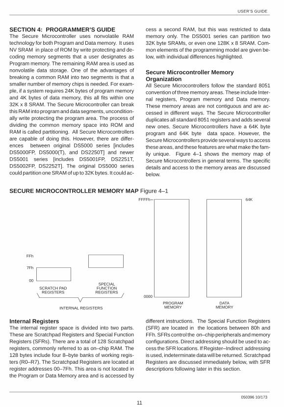
Secure Microcontroller MemoryOrganizationAll Secure Microcontrollers follow the standard 8051convention of three memory areas. These include Inter-nal registers, Program memory and Data memory.These memory areas are not contiguous and are ac-cessed in different ways. The Secure Microcontrollerduplicates all standard 8051 registers and adds severalnew ones. Secure Microcontrollers have a 64K byteprogram and 64K byte data space. However, theSecure Microcontrollers provide several ways to accessthese areas, and these features are what make the fam-ily unique. Figure 4–1 shows the memory map ofSecure Microcontrollers in general terms. The specificdetails and access to the memory areas are discussedbelow.
SECURE MICROCONTROLLER MEMORY MAP Figure 4–1
ÏÏÏÏÏÏÏÏÏÏÏÏÏÏÏÏÏÏÏÏÏÏÏÏÏÏÏÏÏÏÏÏÏÏÏÏÏÏÏÏÏÏÏÏ
ÏÏÏÏÏÏÏÏÏÏÏÏÏÏÏÏÏÏÏÏÏÏÏÏÏÏÏÏÏÏÏÏÏÏÏÏÏÏÏÏÏÏÏÏ
64K
SPECIALFUNCTION
REGISTERSSCRATCH PAD
REGISTERS
INTERNAL REGISTERSPROGRAMMEMORY
DATAMEMORY
0000
FFh
7Fh
00
–FFFFh–
Internal RegistersThe internal register space is divided into two parts.These are Scratchpad Registers and Special FunctionRegisters (SFRs). There are a total of 128 Scratchpadregisters, commonly referred to as on–chip RAM. The128 bytes include four 8–byte banks of working regis-ters (R0–R7). The Scratchpad Registers are located atregister addresses 00–7Fh. This area is not located inthe Program or Data Memory area and is accessed by
different instructions. The Special Function Registers(SFR) are located in the locations between 80h andFFh. SFRs control the on–chip peripherals and memoryconfigurations. Direct addressing should be used to ac-cess the SFR locations. If Register–Indirect addressingis used, indeterminate data will be returned. ScratchpadRegisters are discussed immediately below, with SFRdescriptions following later in this section.

7FH
2FH
2EH
2DH
2CH
2BH
2AH
29H
28H
27H
26H
25H
24H
23H
22H
21H
20H
1FH
18H
17H
10H
0FH
08H
07H
00H
BANK 3
BANK 2
BANK 1
BANK 0
MSB LSB
7F 7E 7D 7C 7B 7A 79 78
77 76 75 74 73 72 71 70
6F 6E 6D 6C 6B 6A 69 68
67 66 65 64 63 62 61 60
5F 5E 5D 5C 5B 5A 59 58
57 56 55 54 53 52 51 50
4F 4E 4D 4C 4B 4A 49 48
47 46 45 44 43 42 41 40
3F 3E 3D 3C 3B 3A 39 38
37 36 35 34 33 32 31 30
2F 2E 2D 2C 2B 2A 28 28
27 26 25 24 23 22 21 20
1F 1E 1D 1C 1B 1A 19 18
17 16 15 14 13 12 11 10
0F 0E 0D 0C 0B 0A 09 08
07 06 05 04 03 02 01 00
USER’S GUIDE
050396 11/173
12
The Scratchpad Registers are general purpose datastorage RAM. They are commonly used for temporarystorage of a small number of variables when high–speed access is needed. Off–chip RAM (MOVX) isused when the quantity of data is larger than 128 bytes.The Scratchpad Registers are lithium backed and willbe preserved in the absence of power.
The Scratchpad area has two additional functions. First,16 bytes of the Scratchpad area are bit addressable.That is, while each byte has an address of its own, thesebits also have individual bit addresses. Certain instruc-tions operate on bits instead of bytes. Although the ad-dresses appear the same, the microprocessor can dis-tinguish a bit address from a byte address by theinstruction used. A large number of individual softwareflags and conditions can be represented using 128(16*8) individually addressable bits.
A second use of the Scratchpad area is for the program-mer’s stack. Like the 8051, the Secure Microcontrolleruses a Stack Pointer (SP – 81h) SFR to direct stack ac-cess into the internal registers. The SP has a default val-ue of 07h. This means that stack storage will begin atlocation 08h. Each PUSH or CALL instruction will incre-ment the SP. Note that while the SP is located in the SFRarea, the stack itself is stored in the Scratchpad area.The Scratchpad Register Memory map is shown inFigure 4–2. Programmer’s note : with the use of ‘C’ com-pilers becoming more frequent, the large memory mod-el should be examined. This compiler model places thestack in off–chip SRAM. Secure Microcontroller basedsystems usually have an abundance of such SRAMcompared to ROM based systems. While off–chip stackresults in slower execution time, the stack size becomesvirtually unlimited.
SCRATCHPAD REGISTER MAP Figure 4–2
USER’S GUIDE
050396 12/173
13
The 8051 instruction set allows efficient (single cycle)access to variables when using the Working Registers.These are a group of four 8–byte banks of ScratchpadRAM. The active Working Registers are referred to asR0–R7. They reside between location 00h and 1Fh, de-pending on which bank is currently selected. Two bits inthe Special Function Register PSW called R1 (PSW.4)
and R0 (PSW.3) are used to determine which is the ac-tive bank. Once selected, all instructions involvingR0–R7 will be directed to the selected group of 8 bytes.This scheme also allows for a fast context switch bysimply changing banks. The following Table shows theoperation of the Register Bank selection.
PSW.4–3 ; R1–R0Register Bank Select Used to select an 8–byte bank of registers to be assigned as R0–R7.
R1 R0 BANK STARTING ADDRESS (R0)
0 0 00h
0 1 08h
1 0 10h
1 1 18h
Program and Data MemoryThe Secure Microcontroller divides its main memory be-tween Program and Data segments. Each map consistsof a 64K byte area from 0000h to FFFFh. Programmemory is inherently read only, since there are no 8051instructions that write to this segment. Data memory isread and write accessible without restrictions. The CPUautomatically routes program fetches to the programarea and MOVX instructions to the data memory area.All of these elements are in common with the standard8051. Secure Microcontroller differences lie in thememory interface, memory map control, and flexibility ofthe memory resources.
Secure Microcontrollers provide two separate buses formemory access. First is a Byte–wide address/data buswhich is new to the 8051 architecture. This bus also pro-vides a switched supply output that make standardSRAM into nonvolatile memory, decoded chip enables,and a R/W strobe. Furthermore, the Byte–wide busallows nonvolatile RAM memory to be divided betweenProgram and Data segments. When using a segment ofthe RAM as Program Memory, this area can be loadedusing the Bootstrap Loader function described later inthis book.
Second is an Expanded bus constituted by Ports 0 and2. This is the standard 8051 compatible memory buswhich is available as an option, but is not needed inmost cases. Program memory on the Expanded bus
must be ROM/EPROM and data memory must be vola-tile SRAM. If NV RAM is needed on the Expanded bus,then it must be externally backed up and write pro-tected. The Secure Microcontroller makes no specialprovisions for NV RAM on the Expanded bus.
When discussing memory addressing of Secure Micro-controllers, there are two important terms that are usedfrequently: Partition and Range. The Partition is theuser–selectable address that divides the program seg-ment from the data segment in a common RAM area onthe Byte–wide bus. The Partition is a user–adjustableboundary that can be selected during Bootstrap Load-ing or on the fly by the application software. The Rangeis the total amount of memory connected to the Byte–wide bus. This is set once during initial programming.
The DS5000 series devices can access between 8Kand 64K bytes of NV RAM on the Byte–wide bus. Up tothe first 32K bytes are Partitionable into Program andData segments as described above. The DS5001 se-ries can access between 8K and 128K bytes on itsByte–wide bus with better Partition control. TheMemory map control resides in the MCON (addressC6h) Special Function Register on DS5000 devices. OnDS5001 devices, both the MCON (address C6h) andRPCTL (address D8h) registers are used. Since thememory maps and control have significant differencesbetween these versions, they are described below inseparate sections.

USER’S GUIDE
050396 13/173
14
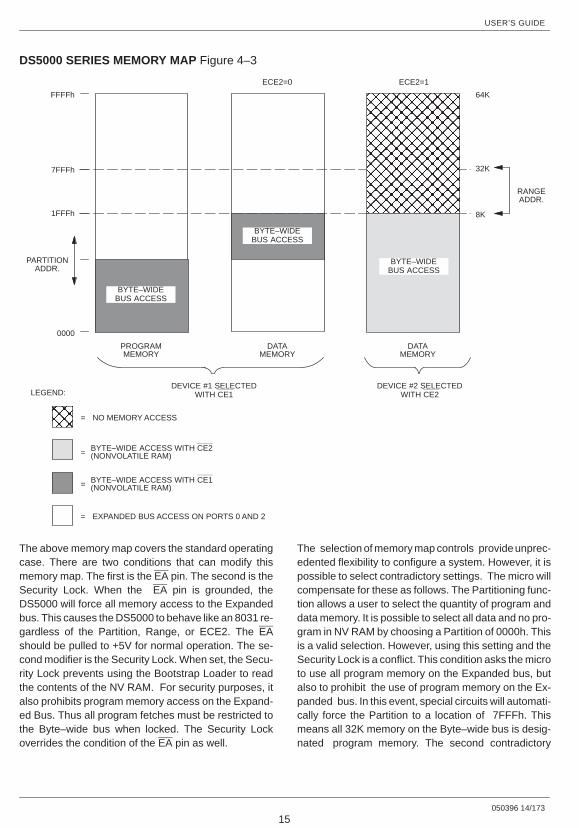
DS5000 Series Memory OrganizationAs mentioned above, the DS5000 series consists of theDS5000FP chip and the DS5000(T) and DS2250T mod-ules. The programming model discussed in this sectionapplies to all of these parts. The DS5000 series Byte–wide bus has 15 address lines, eight data lines, a R/Wstrobe, and two chip enables to access nonvolatileRAM. In the case of a module, these are already con-nected and may be thought of as internal or embeddedmemory. The DS5000 series can use either 8K x 8 or32K x 8 SRAMs. The user must inform the microcontrol-ler of the selected RAM size using the Range function.The Range bit resides in the MCON SFR at MCON.3and has a value of 0 when 8K SRAM is used and 1 whena 32K byte SRAM is used. Range is selected duringBootstrap Loading and can not be varied by the applica-tion software. The DS5000 device accesses memory onits Byte–wide bus using two chip enables. The first,CE1, is Partitionable. That is, the RAM connected toCE1, whether 8K or 32K, can be divided between pro-gram and data segments. The Partition is user–se-lected and can be set during Bootstrap Loading and bysoftware. Partitions are generally available on 2K byteboundaries in the DS5000 except for the last which is4K. The Partition is selected using the MCON SFR de-scribed below. CE2 is restricted to data memory only.The RAM on CE2 should be of the same size as CE1.Access to CE2 is manual, and functions like a bankswitch. Bit 2 (ECE2) of the MCON SFR controls accessto CE2 and is described below.
Figure 4–3 illustrates the functional memory map of aDS5000 series device. The Partition, Range, ECE2,and the logical address combine to determine whetherthe DS5000 uses its Byte–wide bus or the Expanded
Bus. Nonvolatile RAM access will occur when the log-ical address lies in one of the shaded regions. These areprogram addresses below the Partition address, dataaddresses above the Partition and below the Range ad-dress, or data addresses between 0 and the Rangewhen ECE2 is set to a logic 1. Note that when usingECE2 to force data access, the CE2 RAM will be se-lected instead of the CE1 RAM. This means that on aDS5000 module or a DS2250 with less than 64K RAM,no data memory exists under CE2. The ECE2 has noaffect on program memory, which continues from theCE1 RAM or the Expanded bus normally.
Note that the Partition and Range settings are not auto-matically linked. This means a user should take care notto select a Partition that is larger than the Range. Natu-rally when the Range is 32K, the Partition address canbe as high as 32K. When a Range of 8K is used, Parti-tion addresses below 8K should be used. Any addressthat does not map onto the Byte–wide bus will be auto-matically be routed to the Expanded Bus of Ports 0 and2. For module users. this means that any address notrouted to internal memory will go to the ports. The follow-ing examples will help illustrate the decoding.
When the Partition is at 3000h, and the Range at 32K,program memory below 3000h is accessed on theByte–wide bus. Program memory at or above 3000h isdirected to the Expanded bus or Ports 0 and 2. When thePartition is at 5800h and the Range at 32K, datamemory at 0000h is accessed on Ports 0 and 2. Datamemory at 6000h is located in NV RAM on the Byte–wide bus. When the Partition is at 1000h and the Rangeat 8K, all memory access above 1FFFh is on the Ex-panded bus. Below 8K, the Partition rules apply.
IMPORTANT APPLICATION NOTEThe MCON register is a special function register unique to Dallas Semiconductor microcontrollers which containsnonvolatile memory configuration information. This register should be set to the desired value before loading thedevice via the bootstrap loader. Failure to correctly configure the MCON register can cause the device to operateincorrectly, including symptoms which appear similar to a defective device. Because this register is nonvolatile, incor-rect memory settings will be preserved when power is removed. The DS5001FP, DS5002FP, DS2251T, andDS2252T store additional memory configuration information in the RPCTL register, which should also be set to thedesired value before loading the device via the bootstrap loader.
USER’S GUIDE
050396 14/173
15
DS5000 SERIES MEMORY MAP Figure 4–3
BYTE–WIDE ACCESS WITH CE2(NONVOLATILE RAM)
ÑÑÑÑÑÑÑÑÑÑÑÑÑÑÑÑÑÑÑÑÑÑÑÑÑÑÑÑÑÑÑÑÑÑÑÑ
FFFFh
7FFFh
1FFFh
0000
PROGRAM DATA DATA
ÑÑÑÑ
= NO MEMORY ACCESS
LEGEND:
MEMORY MEMORY MEMORY
BYTE–WIDEBUS ACCESS
64K
32K
8K
RANGEADDR.
BYTE–WIDEBUS ACCESS
BYTE–WIDEBUS ACCESS
PARTITIONADDR.
=
ÏÏÏÏ
= EXPANDED BUS ACCESS ON PORTS 0 AND 2
BYTE–WIDE ACCESS WITH CE1(NONVOLATILE RAM)=
ECE2=1ECE2=0
DEVICE #2 SELECTEDWITH CE2
DEVICE #1 SELECTEDWITH CE1
The above memory map covers the standard operatingcase. There are two conditions that can modify thismemory map. The first is the EA pin. The second is theSecurity Lock. When the EA pin is grounded, theDS5000 will force all memory access to the Expandedbus. This causes the DS5000 to behave like an 8031 re-gardless of the Partition, Range, or ECE2. The EAshould be pulled to +5V for normal operation. The se-cond modifier is the Security Lock. When set, the Secu-rity Lock prevents using the Bootstrap Loader to readthe contents of the NV RAM. For security purposes, italso prohibits program memory access on the Expand-ed Bus. Thus all program fetches must be restricted tothe Byte–wide bus when locked. The Security Lockoverrides the condition of the EA pin as well.
The selection of memory map controls provide unprec-edented flexibility to configure a system. However, it ispossible to select contradictory settings. The micro willcompensate for these as follows. The Partitioning func-tion allows a user to select the quantity of program anddata memory. It is possible to select all data and no pro-gram in NV RAM by choosing a Partition of 0000h. Thisis a valid selection. However, using this setting and theSecurity Lock is a conflict. This condition asks the microto use all program memory on the Expanded bus, butalso to prohibit the use of program memory on the Ex-panded bus. In this event, special circuits will automati-cally force the Partition to a location of 7FFFh. Thismeans all 32K memory on the Byte–wide bus is desig-nated program memory. The second contradictory
USER’S GUIDE
050396 15/173
16
case is to select a Range of 8K, and to choose a Parti-tion of greater than 8K. This will result in the Range asthe limiting factor. Addresses above the Range will auto-matically be deflected to the Expanded bus. No datamemory will be allocated in NV RAM for this configura-tion.
DS5000 Memory Map ControlThe Partition and Range can be selected using theBootstrap Loader discussed in a later section. In addi-
tion, the Partition can be selected or modified by the ap-plication software and CE2 is normally software con-trolled. However, in either case, the MCON SFR is usedto choose these settings. The MCON is summarized inthe SFR section below, but appears here also.
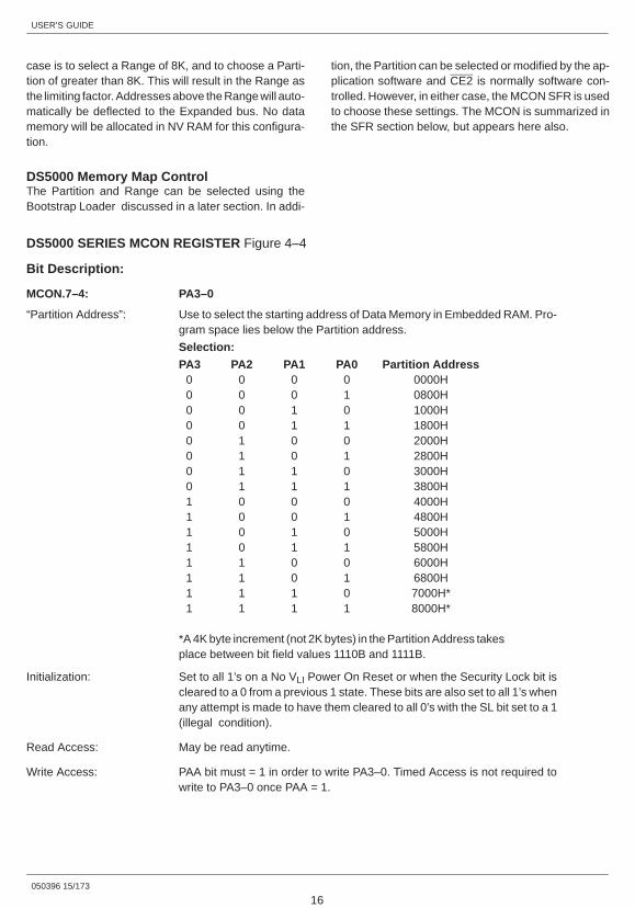
DS5000 SERIES MCON REGISTER Figure 4–4
Bit Description:
MCON.7–4: PA3–0
“Partition Address”: Use to select the starting address of Data Memory in Embedded RAM. Pro-gram space lies below the Partition address.
Selection:
PA3 PA2 PA1 PA0 Partition Address0 0 0 0 0000H0 0 0 1 0800H0 0 1 0 1000H0 0 1 1 1800H0 1 0 0 2000H0 1 0 1 2800H0 1 1 0 3000H0 1 1 1 3800H1 0 0 0 4000H1 0 0 1 4800H1 0 1 0 5000H1 0 1 1 5800H1 1 0 0 6000H1 1 0 1 6800H1 1 1 0 7000H*1 1 1 1 8000H*
*A 4K byte increment (not 2K bytes) in the Partition Address takesplace between bit field values 1110B and 1111B.
Initialization: Set to all 1’s on a No VLI Power On Reset or when the Security Lock bit iscleared to a 0 from a previous 1 state. These bits are also set to all 1’s whenany attempt is made to have them cleared to all 0’s with the SL bit set to a 1(illegal condition).
Read Access: May be read anytime.
Write Access: PAA bit must = 1 in order to write PA3–0. Timed Access is not required towrite to PA3–0 once PAA = 1.
USER’S GUIDE
050396 16/173
17
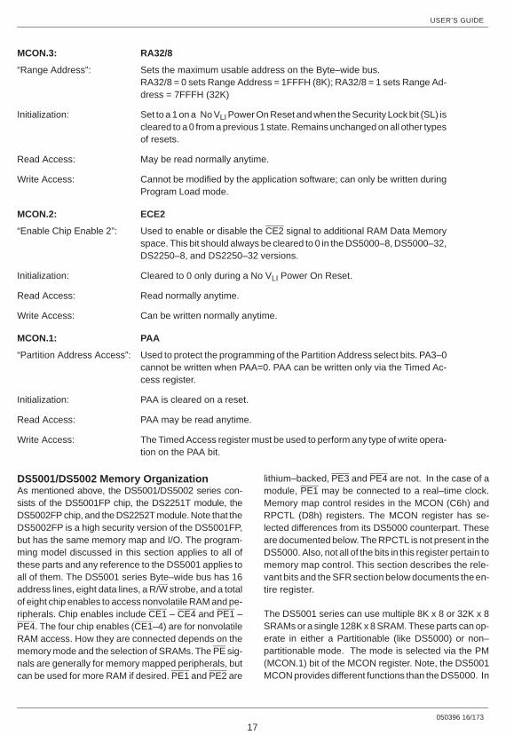
MCON.3: RA32/8
“Range Address”: Sets the maximum usable address on the Byte–wide bus.RA32/8 = 0 sets Range Address = 1FFFH (8K); RA32/8 = 1 sets Range Ad-dress = 7FFFH (32K)
Initialization: Set to a 1 on a No VLI Power On Reset and when the Security Lock bit (SL) iscleared to a 0 from a previous 1 state. Remains unchanged on all other typesof resets.
Read Access: May be read normally anytime.
Write Access: Cannot be modified by the application software; can only be written duringProgram Load mode.
MCON.2: ECE2
“Enable Chip Enable 2”: Used to enable or disable the CE2 signal to additional RAM Data Memoryspace. This bit should always be cleared to 0 in the DS5000–8, DS5000–32,DS2250–8, and DS2250–32 versions.
Initialization: Cleared to 0 only during a No VLI Power On Reset.
Read Access: Read normally anytime.
Write Access: Can be written normally anytime.
MCON.1: PAA
“Partition Address Access”: Used to protect the programming of the Partition Address select bits. PA3–0cannot be written when PAA=0. PAA can be written only via the Timed Ac-cess register.
Initialization: PAA is cleared on a reset.
Read Access: PAA may be read anytime.
Write Access: The Timed Access register must be used to perform any type of write opera-tion on the PAA bit.
DS5001/DS5002 Memory OrganizationAs mentioned above, the DS5001/DS5002 series con-sists of the DS5001FP chip, the DS2251T module, theDS5002FP chip, and the DS2252T module. Note that theDS5002FP is a high security version of the DS5001FP,but has the same memory map and I/O. The program-ming model discussed in this section applies to all ofthese parts and any reference to the DS5001 applies toall of them. The DS5001 series Byte–wide bus has 16address lines, eight data lines, a R/W strobe, and a totalof eight chip enables to access nonvolatile RAM and pe-ripherals. Chip enables include CE1 – CE4 and PE1 –PE4. The four chip enables (CE1–4) are for nonvolatileRAM access. How they are connected depends on thememory mode and the selection of SRAMs. The PE sig-nals are generally for memory mapped peripherals, butcan be used for more RAM if desired. PE1 and PE2 are
lithium–backed, PE3 and PE4 are not. In the case of amodule, PE1 may be connected to a real–time clock.Memory map control resides in the MCON (C6h) andRPCTL (D8h) registers. The MCON register has se-lected differences from its DS5000 counterpart. Theseare documented below. The RPCTL is not present in theDS5000. Also, not all of the bits in this register pertain tomemory map control. This section describes the rele-vant bits and the SFR section below documents the en-tire register.
The DS5001 series can use multiple 8K x 8 or 32K x 8SRAMs or a single 128K x 8 SRAM. These parts can op-erate in either a Partitionable (like DS5000) or non–partitionable mode. The mode is selected via the PM(MCON.1) bit of the MCON register. Note, the DS5001MCON provides different functions than the DS5000. In

USER’S GUIDE
050396 17/173
18
a Partitionable mode (PM=0), the DS5001 can use upto 64K x 8 SRAM for program and data on its Byte–widebus. It can partition this area into program and datasegments on 4K boundaries. The 64K memory spacewould consist of two 32K x 8 SRAMs. Each is accessedby a separate chip enable (CE1 and CE2), but the mi-crocontroller automatically decodes which is needed.While the DS5001 can use between one 8K x 8 SRAMand 4 32K x 8 SRAMs, it does not automatically know
which configuration is used. The Range function deter-mines how much total memory is connected to theByte–wide bus. The user must identify the total RAMsize using the Range bits RG1 and RG0. RG1 is lo-cated at MCON.3 and RG0 is located at RPCTL.0.These Range bits are selected during the BootstrapLoading process and can not be modified by the ap-plication software. The Table below shows the Rangevalues that can be selected when PM=0 (Partitionable).
RG1 RG0 RANGE CE1 ACCESS CE2 ACCESS
1 1 64K 0000–7FFFh 8000–FFFFh
1 0 32K 0000–7FFFh NA
0 1 16K 0000–1FFFh 2000h–3FFFh
0 0 8K 0000–1FFFh NA
The total RAM space is partitionable, regardless ofwhich Range is selected. This contrasts with theDS5000 that allowed partitioning of CE1 only. ThePartition table is shown below. PA3–0 are the four MSBsof the MCON register (MCON.7–4). Note that the Parti-tion values do not scale depending on Range. That is, if
a Range of less than 64K is selected, then the partitionsettings above the Range should not be unused. Themicrocontroller automatically decodes which RAM toenable, and uses the Partition to decide if this is pro-gram memory or data memory.
PA3 PA2 PA1 PA0 PARTITION BYTE–WIDE BUS MEMORY MAP
0 0 0 0 0000h 0K PROGRAM, DATA = RANGE
0 0 0 1 1000h 4K PROGRAM, DATA = RANGE – 4K
0 0 1 0 2000h 8K PROGRAM, DATA = RANGE – 8K
0 0 1 1 3000h 12K PROGRAM, DATA = RANGE – 12K
0 1 0 0 4000h 16K PROGRAM, DATA = RANGE – 16K
0 1 0 1 5000h 20K PROGRAM, DATA = RANGE – 20K
0 1 1 0 6000h 24K PROGRAM, DATA = RANGE – 24K
0 1 1 1 7000h 28K PROGRAM, DATA = RANGE – 28K
1 0 0 0 8000h 32K PROGRAM, DATA = RANGE – 32K
1 0 0 1 9000h 36K PROGRAM, 28K DATA
1 0 1 0 A000h 40K PROGRAM, 24K DATA
1 0 1 1 B000h 44K PROGRAM, 20K DATA
1 1 0 0 C000h 48K PROGRAM, 16K DATA
1 1 0 1 D000h 52K PROGRAM, 12K DATA
1 1 1 0 E000h 56K PROGRAM, 8K DATA
1 1 1 1 FFFFh 64K PROGRAM, 0K DATA
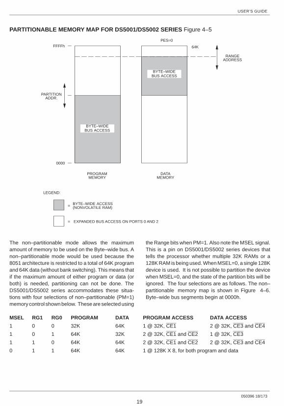
Figure 4–5 illustrates the functional memory map of aDS5001 series device in Partitionable mode. Note thatlike the DS5000, any access that does not correspond
to a Byte–wide bus location is routed to the Expandedbus Ports 0 and 2.
USER’S GUIDE
050396 18/173
19
PARTITIONABLE MEMORY MAP FOR DS5001/DS5002 SERIES Figure 4–5
FFFFh
0000
PROGRAM DATA
LEGEND:
BYTE–WIDEBUS ACCESS
BYTE–WIDEBUS ACCESS
PARTITIONADDR.
ÏÏÏÏ
= EXPANDED BUS ACCESS ON PORTS 0 AND 2
BYTE–WIDE ACCESS(NONVOLATILE RAM)=
PES=0
64K
RANGEADDRESS
MEMORY MEMORY
The non–partitionable mode allows the maximumamount of memory to be used on the Byte–wide bus. Anon–partitionable mode would be used because the8051 architecture is restricted to a total of 64K programand 64K data (without bank switching). This means thatif the maximum amount of either program or data (orboth) is needed, partitioning can not be done. TheDS5001/DS5002 series accommodates these situa-tions with four selections of non–partitionable (PM=1)memory control shown below. These are selected using
the Range bits when PM=1. Also note the MSEL signal.This is a pin on DS5001/DS5002 series devices thattells the processor whether multiple 32K RAMs or a128K RAM is being used. When MSEL=0, a single 128Kdevice is used. It is not possible to partition the devicewhen MSEL=0, and the state of the partition bits will beignored. The four selections are as follows. The non–partitionable memory map is shown in Figure 4–6.Byte–wide bus segments begin at 0000h.
MSEL RG1 RG0 PROGRAM DATA PROGRAM ACCESS DATA ACCESS
1 0 0 32K 64K 1 @ 32K, CE1 2 @ 32K, CE3 and CE4
1 0 1 64K 32K 2 @ 32K, CE1 and CE2 1 @ 32K, CE3
1 1 0 64K 64K 2 @ 32K, CE1 and CE2 2 @ 32K, CE3 and CE4
0 1 1 64K 64K 1 @ 128K X 8, for both program and data
USER’S GUIDE
050396 19/173
20
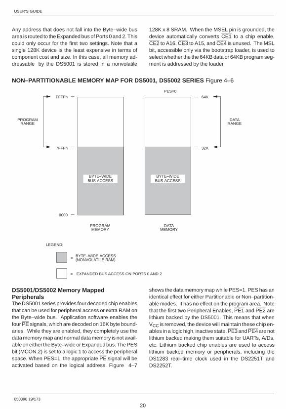
Any address that does not fall into the Byte–wide busarea is routed to the Expanded bus of Ports 0 and 2. Thiscould only occur for the first two settings. Note that asingle 128K device is the least expensive in terms ofcomponent cost and size. In this case, all memory ad-dressable by the DS5001 is stored in a nonvolatile
128K x 8 SRAM. When the MSEL pin is grounded, thedevice automatically converts CE1 to a chip enable,CE2 to A16, CE3 to A15, and CE4 is unused. The MSLbit, accessible only via the bootstrap loader, is used toselect whether the the 64KB data or 64KB program seg-ment is addressed by the loader.
NON–PARTITIONABLE MEMORY MAP FOR DS5001, DS5002 SERIES Figure 4–6
FFFFh
0000
PROGRAM DATA
LEGEND:
BYTE–WIDEBUS ACCESS
BYTE–WIDEBUS ACCESS
ÏÏÏÏ
= EXPANDED BUS ACCESS ON PORTS 0 AND 2
BYTE–WIDE ACCESS(NONVOLATILE RAM)=
PES=0
64K
32K7FFFh
DATARANGE
PROGRAMRANGE
MEMORY MEMORY
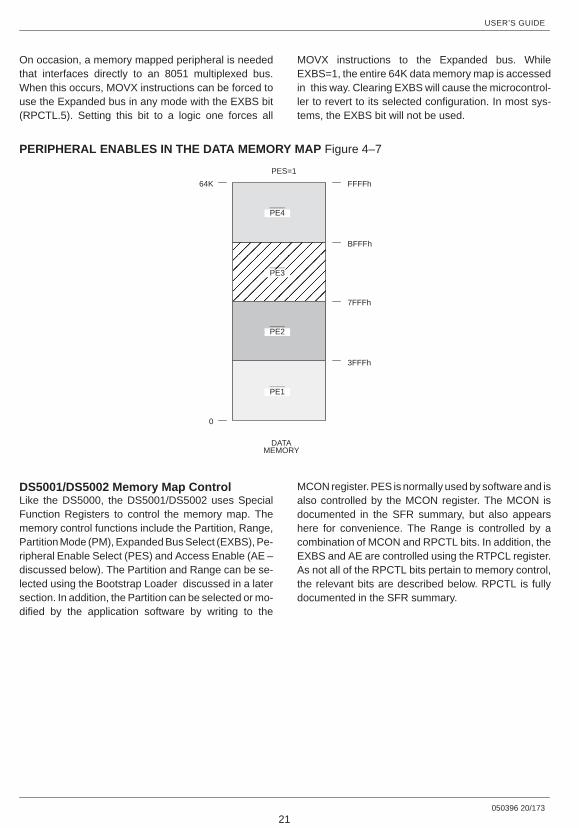
DS5001/DS5002 Memory MappedPeripheralsThe DS5001 series provides four decoded chip enablesthat can be used for peripheral access or extra RAM onthe Byte–wide bus. Application software enables thefour PE signals, which are decoded on 16K byte bound-aries. While they are enabled, they completely use thedata memory map and normal data memory is not avail-able on either the Byte–wide or Expanded bus. The PESbit (MCON.2) is set to a logic 1 to access the peripheralspace. When PES=1, the appropriate PE signal will beactivated based on the logical address. Figure 4–7
shows the data memory map while PES=1. PES has anidentical effect for either Partitionable or Non–partition-able modes. It has no effect on the program area. Notethat the first two Peripheral Enables, PE1 and PE2 arelithium backed by the DS5001. This means that whenVCC is removed, the device will maintain these chip en-ables in a logic high, inactive state. PE3 and PE4 are notlithium backed making them suitable for UARTs, A/Ds,etc. Lithium backed chip enables are used to accesslithium backed memory or peripherals, including theDS1283 real–time clock used in the DS2251T andDS2252T.
USER’S GUIDE
050396 20/173
21
On occasion, a memory mapped peripheral is neededthat interfaces directly to an 8051 multiplexed bus.When this occurs, MOVX instructions can be forced touse the Expanded bus in any mode with the EXBS bit(RPCTL.5). Setting this bit to a logic one forces all
MOVX instructions to the Expanded bus. WhileEXBS=1, the entire 64K data memory map is accessedin this way. Clearing EXBS will cause the microcontrol-ler to revert to its selected configuration. In most sys-tems, the EXBS bit will not be used.
PERIPHERAL ENABLES IN THE DATA MEMORY MAP Figure 4–7
ÏÏÏÏÏÏÏÏÏÏÏÏÏÏÏÏÏÏÏÏ
DATAMEMORY
PES=1
PE1
PE2
PE3
PE4
FFFFh
BFFFh
7FFFh
3FFFh
64K
0
DS5001/DS5002 Memory Map ControlLike the DS5000, the DS5001/DS5002 uses SpecialFunction Registers to control the memory map. Thememory control functions include the Partition, Range,Partition Mode (PM), Expanded Bus Select (EXBS), Pe-ripheral Enable Select (PES) and Access Enable (AE –discussed below). The Partition and Range can be se-lected using the Bootstrap Loader discussed in a latersection. In addition, the Partition can be selected or mo-dified by the application software by writing to the
MCON register. PES is normally used by software and isalso controlled by the MCON register. The MCON isdocumented in the SFR summary, but also appearshere for convenience. The Range is controlled by acombination of MCON and RPCTL bits. In addition, theEXBS and AE are controlled using the RTPCL register.As not all of the RPCTL bits pertain to memory control,the relevant bits are described below. RPCTL is fullydocumented in the SFR summary.

USER’S GUIDE
050396 21/173
22
DS5001/DS5002 SERIES MCON REGISTER Figure 4–8
PA3 PA2 PA1 PA0 RG1 PES PM –––
Bit Description:
MCON.7–4: PA3–0Partition Address. When PM=0, this address specifies the boundarybetween program and data memory in a continuous space.
Initialization: Unaffected by watchdog, external, or power–up resets. Set to 1111B on aNo VLI reset.
Read Access: Can be read normally at any time.
Write Access: Timed Access Protected. Also, cannot be written by the application soft-ware if set to 0000B by the serial loader. If a 0000B is written via the serialloader and the security lock is set, the Partition will become 1111B. Thesame will occur if write access is available and application software writes a0000B. In addition, these bits will be set to 1111B if security lock is cleared.
MCON.3: RG1One of two bits that determine the range of program space. RG0 is locatedin the RPCTL register.
Initialization: Unaffected by watchdog, external, or power–up resets. Set to 1 on a No VLIreset or a clearing of the security lock.
Read Access: Can be read at any time.
Write Access: Cannot be modified by the application software. Can only be written duringprogram load.
MCON.2: PESPeripheral Enable Select. When this bit is set, the data space is controlledby PE1 – PE4. Peripherals are memory–mapped in 16K blocks, and areaccessed by MOVX instructions.
Initialization: Cleared by all resets.
Read Access: Can be read at any time.
Write Access: Can be written at any time.
MCON.1: PMPartition Mode. When PM=0, a partitionable, continuous memory map isinvoked. When PM=1, one of four fixed allocations is used.
Initialization: Unaffected by watchdog, external, or power–up reset. Cleared on a No VLIreset.
Read Access: Can be read at any time.
Write Access: Cannot be written by the application software. Can only be modified duringprogram load.

USER’S GUIDE
050396 22/173
23
DS5001/DS5002 SERIES RPCTL REGISTER BITS AFFECTING MEMORY Figure 4–9
RNR ––– EXBS AE IBI DMA RPCON RG0
Bit Description:
RPCTL.5: EXBSThe Expanded Bus Select routes data memory access (MOVX) to theExpanded bus formed by ports 0 and 2 when set.
Initialization: Cleared after all resets.
Read Access: Can be read at any time.
Write Access: Can be written at any time.
RPCTL.4: AEAccess Enable is used when a software reload is desired without usingProgram Load mode. When set, the DS5001 will be temporarily configuredin a Partitionable configuration with the partition at 4K. This will occur evenif the PM=1. When cleared, the prior memory configuration is resumed.
Initialization: Cleared after all resets.
Read Access: Can be read at any time.
Write Access: Can be written at any time, timed access protected.
RPCTL.0: RG0This is a Range bit which is used to determine the size of the programmemory space. Its usage is shown above.
Initialization: Unaffected by watchdog, external, or power–up resets. Cleared on a No VLIreset or clearing of the security lock.
Read Access: Can be read at any time.
Write Access: Cannot be modified by the application software. Can only be written duringProgram Load.
Loading and Reloading Program MemorySoft Microcontrollers are programmed through a built–in Bootstrap Loader function. This loader is also used toconfigure the desired options for memory map control.The Secure Microcontroller uses its low power lithiumbacked circuits to maintain critical settings in the ab-sence of power. For this reason, it is not necessary to setthe Partition, Range, etc. after every power–up or reset.Once set, they will remain unless deliberately modified.Bootstrap Loading is discussed in a later section. Oneof the major advantages of a Secure Microcontroller isthe ability to change these settings, and even reload theentire program memory while the device is installed insystem. To completely re–program and re–configure a
device, the Bootstrap Loader must be invoked. Howev-er, the Secure Microcontroller is designed to allow apartial reload of memory without invoking the BootstrapLoader.
The major advantage of this technique is that it requiresno hardware or external switches. Most of the memorycan be reprogrammed under application software con-trol. It would commonly be used when the target systemconnects to a PC through a serial port as part of an ap-plication. For example, a data logger that must dumpmemory periodically. While connected to the PC, it isextremely easy to reload portions of memory using the“Soft Reload”.
USER’S GUIDE
050396 23/173
24
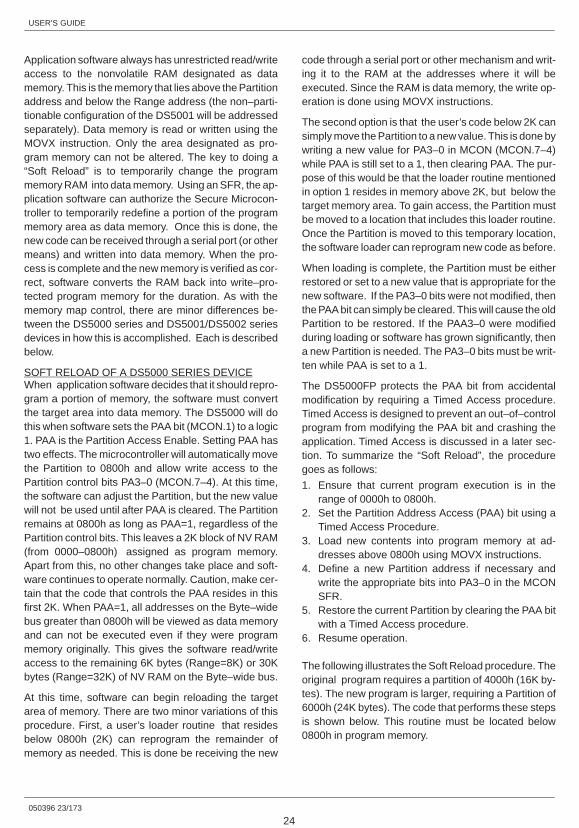
Application software always has unrestricted read/writeaccess to the nonvolatile RAM designated as datamemory. This is the memory that lies above the Partitionaddress and below the Range address (the non–parti-tionable configuration of the DS5001 will be addressedseparately). Data memory is read or written using theMOVX instruction. Only the area designated as pro-gram memory can not be altered. The key to doing a“Soft Reload” is to temporarily change the programmemory RAM into data memory. Using an SFR, the ap-plication software can authorize the Secure Microcon-troller to temporarily redefine a portion of the programmemory area as data memory. Once this is done, thenew code can be received through a serial port (or othermeans) and written into data memory. When the pro-cess is complete and the new memory is verified as cor-rect, software converts the RAM back into write–pro-tected program memory for the duration. As with thememory map control, there are minor differences be-tween the DS5000 series and DS5001/DS5002 seriesdevices in how this is accomplished. Each is describedbelow.
SOFT RELOAD OF A DS5000 SERIES DEVICEWhen application software decides that it should repro-gram a portion of memory, the software must convertthe target area into data memory. The DS5000 will dothis when software sets the PAA bit (MCON.1) to a logic1. PAA is the Partition Access Enable. Setting PAA hastwo effects. The microcontroller will automatically movethe Partition to 0800h and allow write access to thePartition control bits PA3–0 (MCON.7–4). At this time,the software can adjust the Partition, but the new valuewill not be used until after PAA is cleared. The Partitionremains at 0800h as long as PAA=1, regardless of thePartition control bits. This leaves a 2K block of NV RAM(from 0000–0800h) assigned as program memory.Apart from this, no other changes take place and soft-ware continues to operate normally. Caution, make cer-tain that the code that controls the PAA resides in thisfirst 2K. When PAA=1, all addresses on the Byte–widebus greater than 0800h will be viewed as data memoryand can not be executed even if they were programmemory originally. This gives the software read/writeaccess to the remaining 6K bytes (Range=8K) or 30Kbytes (Range=32K) of NV RAM on the Byte–wide bus.
At this time, software can begin reloading the targetarea of memory. There are two minor variations of thisprocedure. First, a user’s loader routine that residesbelow 0800h (2K) can reprogram the remainder ofmemory as needed. This is done be receiving the new
code through a serial port or other mechanism and writ-ing it to the RAM at the addresses where it will beexecuted. Since the RAM is data memory, the write op-eration is done using MOVX instructions.
The second option is that the user’s code below 2K cansimply move the Partition to a new value. This is done bywriting a new value for PA3–0 in MCON (MCON.7–4)while PAA is still set to a 1, then clearing PAA. The pur-pose of this would be that the loader routine mentionedin option 1 resides in memory above 2K, but below thetarget memory area. To gain access, the Partition mustbe moved to a location that includes this loader routine.Once the Partition is moved to this temporary location,the software loader can reprogram new code as before.
When loading is complete, the Partition must be eitherrestored or set to a new value that is appropriate for thenew software. If the PA3–0 bits were not modified, thenthe PAA bit can simply be cleared. This will cause the oldPartition to be restored. If the PAA3–0 were modifiedduring loading or software has grown significantly, thena new Partition is needed. The PA3–0 bits must be writ-ten while PAA is set to a 1.
The DS5000FP protects the PAA bit from accidentalmodification by requiring a Timed Access procedure.Timed Access is designed to prevent an out–of–controlprogram from modifying the PAA bit and crashing theapplication. Timed Access is discussed in a later sec-tion. To summarize the “Soft Reload”, the proceduregoes as follows:
1. Ensure that current program execution is in therange of 0000h to 0800h.
2. Set the Partition Address Access (PAA) bit using aTimed Access Procedure.
3. Load new contents into program memory at ad-dresses above 0800h using MOVX instructions.
4. Define a new Partition address if necessary andwrite the appropriate bits into PA3–0 in the MCONSFR.
5. Restore the current Partition by clearing the PAA bitwith a Timed Access procedure.
6. Resume operation.
The following illustrates the Soft Reload procedure. Theoriginal program requires a partition of 4000h (16K by-tes). The new program is larger, requiring a Partition of6000h (24K bytes). The code that performs these stepsis shown below. This routine must be located below0800h in program memory.
USER’S GUIDE
050396 24/173
25
MOV TA, #0AAh ; TIMED ACCESS
MOV TA, #55h ; TIMED ACCESS 2
MOV MCON, #10001010b ; SET PAA BIT
. ; USER’S CODE TO LOAD
. ; RAM USING MOVX
.
.
MOV TA, #0AAh ; TIMED ACCESS
MOV TA, #55h ; TIMED ACCESS 2
MOV MCON, #11001000b ; LOAD NEW PARTITION AND CLEAR PAA BIT
RELOADING PORTIONS OF A DS5000 SERIES DEVICE Figure 4–10
7FFFh
6000h
4000h
0000h
LEGEND:
PROGRAMMEMORY
SPACE
=
=
DATAMEMORY
SPACE
DATAMEMORY
SPACE
PROGRAMMEMORY
SPACE
PROGRAMMEMORY
SPACE
BEFORE LOADINGPAA=0PA3–0=1000b
DURING LOADINGPAA=1PA3–0=XXXXb
AFTER LOADINGPAA=0PA3–0=1100b
DATAMEMORY
SPACE
0800h
RANGE (32K)
NEW PARTITION (24K)
OLD PARTITION (16K)
0K
TEMP PARTITION (2K)
NONVOLATILE RAM PROGRAM MEMORY
NONVOLATILE RAM DATA MEMORY
USER’S GUIDE
050396 25/173
26
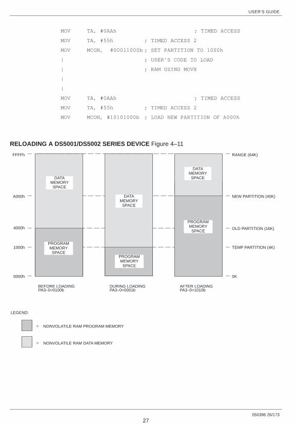
SOFT RELOAD OF A DS5001/DS5002When application software decides that it should repro-gram a portion of memory, the software must convertthe target area into data memory. However, a Soft Re-load of a DS5001 series device has minor variationsfrom the DS5000 version. First, there is no PAA bit in theDS5001. If the DS5001 is in a Partitionable mode thenthe user’s program must manipulate the Partition con-trol bits PA3–0, placing the Partition to a value that per-mits the target area to be loaded. Moving the Partition toa new value should convert the target area to datamemory allowing read/write access. The user’s loaderroutine then uses MOVX instructions to load the newprogram contents into memory. This program can be re-ceived from a serial port or other mechanism. When theloading procedure is complete, a new Partition (or theold one) must be loaded. Note that the loader routinemust reside below the Partition at all times.
In the DS5000 series, the PAA bit was protected by aTimed Access procedure. In the DS5001, the PA3–0bits are protected directly. The user’s program must usea Timed Access procedure to alter these bits. The mi-crocontroller further protects the application by not per-mitting software to write a 0000b into PA3–0. This wouldcause a program memory area of 0K. Timed Access isdiscussed in a later section.
If the device is in a non–partitionable configuration, thenan extra step is required. To perform a Soft Reload of theprogram contents in a non–partitionable mode, the soft-ware must convert the micro to a Partitionable modetemporarily. The Access Enable bit (RPCTL.4) will ac-complish this. Setting the AE bit to a logic 1 converts theDS5001 into a Partitionable mode for as long as it is set.This means that regardless of the original setting, onceAE=1, the memory map is a 64K partitionable mode.The Partition is set to 1000h (4K) when AE=1, so theloader routine must reside in this area. The user canthen perform the Soft Reload as discussed above.When loading is complete, the software should clear the
AE bit. Note that AE requires software to use a TimedAccess procedure to alter it. This method allows a userto alter program memory in a non–partitionable mode.Data memory can be initialized by application softwareat any time. Since full read/write access is available, nospecial provisions are needed.
To summarize the “Soft Reload” for a DS5001/DS5002,the procedure goes as follows:
Partitionable mode1. Write a value to PA3–0 using a Timed Access that
gives access to the target area of memory.
2. Load new contents into program memory at ad-dresses above the Partition using MOVX instruc-tions.
3. Define a new Partition address if necessary andwrite the appropriate bits into PA3–0 in the MCONSFR using a Timed Access.
4. Resume operation.
Non–Partitionable mode1. Set the AE bit to a 1 using a Timed Access proce-
dure.
2. Load new contents into program memory at ad-dresses above the Partition (4K) using MOVXinstructions.
3. Clear the AE bit using a Timed Access procedure.
4. Resume operation.
The following illustrates an example where a Soft Re-load is performed for a Partitionable mode. The originalprogram requires a partition of 4000h (16K bytes). Thenew program is larger, requiring a Partition of A000h(40K bytes). A loader routine resides below address1000h. The code that performs these steps is shown be-low. Note that the Timed Access procedure is per-formed, but is described in a later section.
USER’S GUIDE
050396 26/173
27
MOV TA, #0AAh ; TIMED ACCESS
MOV TA, #55h ; TIMED ACCESS 2
MOV MCON, #00011000b ; SET PARTITION TO 1000h
| ; USER’S CODE TO LOAD
| ; RAM USING MOVX
|
|
MOV TA, #0AAh ; TIMED ACCESS
MOV TA, #55h ; TIMED ACCESS 2
MOV MCON, #10101000b ; LOAD NEW PARTITION OF A000h
RELOADING A DS5001/DS5002 SERIES DEVICE Figure 4–11
FFFFh
A000h
4000h
0000h
LEGEND:
PROGRAMMEMORY
SPACE
=
=
DATAMEMORY
SPACE
DATAMEMORY
SPACE
PROGRAMMEMORY
SPACE
PROGRAMMEMORY
SPACE
BEFORE LOADINGPA3–0=0100b
DURING LOADINGPA3–0=0001b
AFTER LOADINGPA3–0=1010b
DATAMEMORY
SPACE
1000h
RANGE (64K)
NEW PARTITION (40K)
OLD PARTITION (16K)
0K
TEMP PARTITION (4K)
NONVOLATILE RAM PROGRAM MEMORY
NONVOLATILE RAM DATA MEMORY
USER’S GUIDE
050396 27/173
28
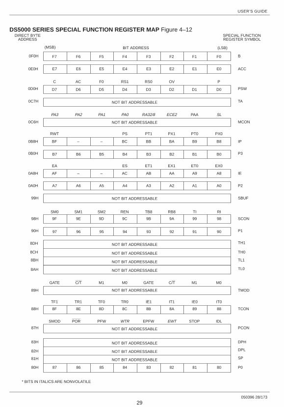
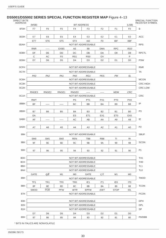
Special Function RegistersThe Secure Microcontroller uses Special Function Reg-isters (SFRs) to control most functions. In many cases,an SFR will contain 8 bits, each of which control a func-tion or report status on a function. The SFRs reside inregister locations 80–FFh. They can be accessed usingMOV instructions with direct addressing. In addition,some of the SFRs are bit addressable. This can be par-ticularly useful when enabling a function without modify-ing others in the register since an SFR can contain 8 un-related control and status functions.
With a few minor exceptions documented below, theSecure Microcontroller provides identical SFRs to astandard 8051, plus extra locations to control uniquefunctions. Modifications to the standard 8051 SFR mapare as follows. The PCON register GF1 (PCON.3) andGF0 (PCON.2) have been replaced by the Enable Pow-er Fail Interrupt and the Enable Watchdog Timer bits re-
spectively. In addition, the Secure Microcontroller re-quires a Timed Access procedure before allowingsoftware to modify the STOP mode bit (PCON.1). This isto prevent errant software from creating a situation thatthe Watchdog Timer can not recover from. The remain-ing SFRs are either identical to the 8051 or new to thearchitecture.
As with the memory map, there are some differencesbetween the DS5000 series and the DS5001 seriesSFRs. Figures 4–12 and 4–13 show an overview of theirrespective SFR maps. Following these figures are de-tailed descriptions. In the case where a particular SFRhas differences between the DS5000 andDS5001/DS5002, those differences will be pointed outunder the particular register. In some cases, theDS5001 and DS5002 have registers that do not appearin the DS5000. This is also highlighted under the partic-ular register.
F7 F6 F5 F4 F3 F2 F1 F0
E7 E6 E5 E4 E3 E2 E1 E0
C AC F0 RS1 RS0 OV P
D7 D6 D5 D4 D3 D2 D1 D0
PA3 PA2 PA1 PA0 RA32/8 ECE2 PAA SL
RWT PS PT1 PX1 PT0 PX0
BF – – BC BB BA B9 B8
B7 B6 B5 B4 B3 B2 B1 B0
EA ES ET1 EX1 ET0 EX0
AF – – AC AB AA A9 A8
A7 A6 A5 A4 A3 A2 A1 A0
SM0 SM1 SM2 REN TB8 RB8 TI RI
9F 9E 9D 9C 9B 9A 99 98
97 96 95 94 93 92 91 90
GATE C/T M1 M0 GATE C/T M1 M0
TF1 TR1 TF0 TR0 IE1 IT1 IE0 IT0
8F 8E 8D 8C 8B 8A 89 88
SMOD POR PFW WTR EPFW EWT STOP IDL
DIRECT BYTEADDRESS
SPECIAL FUNCTIONREGISTER SYMBOL
BIT ADDRESS
NOT BIT ADDRESSABLE
NOT BIT ADDRESSABLE
NOT BIT ADDRESSABLE
NOT BIT ADDRESSABLE
NOT BIT ADDRESSABLE
NOT BIT ADDRESSABLE
NOT BIT ADDRESSABLE
NOT BIT ADDRESSABLE
NOT BIT ADDRESSABLE
NOT BIT ADDRESSABLE
NOT BIT ADDRESSABLE
NOT BIT ADDRESSABLE
87 86 85 84 83 82 81 80
0F0H
0E0H
0D0H
0C7H
0C6H
0B8H
0B0H
0A8H
0A0H
99H
98H
90H
8DH
8CH
8BH
8AH
89H
88H
87H
83H
82H
81H
80H
B
ACC
PSW
TA
MCON
IP
P3
IE
P2
SBUF
SCON
P1
TH1
TH0
TL1
TL0
TMOD
TCON
PCON
DPH
DPL
SP
P0
(MSB) (LSB)
* BITS IN ITALICS ARE NONVOLATILE
USER’S GUIDE
050396 28/173
29
DS5000 SERIES SPECIAL FUNCTION REGISTER MAP Figure 4–12
C/TC/TC/T
WTRPOR
DIRECT BYTEADDRESS
SPECIAL FUNCTIONREGISTER SYMBOL
(MSB) (LSB)BIT ADDRESS
F7 F6 F5 F4 F3 F2 F1 F0
E7 E6 E5 E4 E3 E2 E1 E0
0F0H
0E0H
NOT BIT ADDRESSABLE
ST7 ST6 ST5 ST4 IA0 F0 IBF 0BF
0DAH
B
ACC
RPS
RNR ––– EXBS AE IBI DMA RPC RG0
0D8H RPCTL
C AC F0 RS1 RS0 OV P
0D0H PSW
NOT BIT ADDRESSABLE0CFH RNR
NOT BIT ADDRESSABLE0C7H TA
NOT BIT ADDRESSABLE0C6H MCON
NOT BIT ADDRESSABLE0C3H CRC HIGH
NOT BIT ADDRESSABLE0C2H CRC LOW
NOT BIT ADDRESSABLE0C1H CRC
PA3 PA2 PA1 PA0 RG1 PES PM SL
RNGE3 RNGE2 RNGE1 RNGE0 ––– ––– MDM CRC
RWT PS PT1 PX1 PT0 PX0
0B8H IP
0B0H P3
EA ES ET1 EX1 ET0 EX0
0A8H IE
0A0H P2
NOT BIT ADDRESSABLE99H SBUF
SM0 SM1 SM2 REN TB8 RB8 TI RI
98H SCON
90H P1
NOT BIT ADDRESSABLE8DH TH1
NOT BIT ADDRESSABLE8CH TH0
NOT BIT ADDRESSABLE8BH TL1
NOT BIT ADDRESSABLE8AH TL0
GATE M1 M0 GATE M1 M0
89H TMOD
TF1 TR1 TF0 TR0 IE1 IT1 IE0 IT0
88H TCON
NOT BIT ADDRESSABLE87H PCON
NOT BIT ADDRESSABLE83H DPH
NOT BIT ADDRESSABLE82H DPL
NOT BIT ADDRESSABLE81H SP
D7 D6 D5 D4 D3 D2 D1 D0
80H P0/DBB
DF DE DD DC DB DA D9 D8
D7 D6 D5 D4 D3 D2 D1 D0
BF ––– ––– BC BB BA B9 B8
B7 B6 B5 B4 B3 B2 B1 B0
AF ––– ––– AC AB AA A9 A8
A7 A6 A5 A4 A3 A2 A1 A0
97 96 95 94 93 92 91 90
9F 9E 9D 9C 9B 9A 99 98
8F 8E 8D 8C 8B 8A 89 88
87 86 85 84 83 82 81 80
NOT BIT ADDRESSABLE
SMOD PFW EPFW EWT STOP IDL
* BITS IN ITALICS ARE NONVOLATILE
USER’S GUIDE
050396 29/173
30
DS5001/DS5002 SERIES SPECIAL FUNCTION REGISTER MAP Figure 4–13
USER’S GUIDE
050396 30/173
31
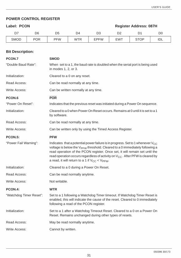
POWER CONTROL REGISTER
Label: PCON Register Address: 087H
D7 D6 D5 D4 D3 D2 D1 D0
SMOD POR PFW WTR EPFW EWT STOP IDL
Bit Description:
PCON.7 SMOD
“Double Baud Rate”: When set to a 1, the baud rate is doubled when the serial port is being usedin modes 1, 2, or 3.
Initialization: Cleared to a 0 on any reset.
Read Access: Can be read normally at any time.
Write Access: Can be written normally at any time.
PCON.6 POR
“Power On Reset”: Indicates that the previous reset was initiated during a Power On sequence.
Initialization: Cleared to a 0 when Power On Reset occurs. Remains at 0 until it is set to a 1by software.
Read Access: Can be read normally at any time.
Write Access: Can be written only by using the Timed Access Register.
PCON.5: PFW
“Power Fail Warning”: Indicates that a potential power failure is in progress. Set to 1 whenever VCCvoltage is below the VPFW threshold. Cleared to a 0 immediately following aread operation of the PCON register. Once set, it will remain set until theread operation occurs regardless of activity on VCC. After PFW is cleared bya read, it will return to a 1 if VCC < VPFW.
Initialization: Cleared to a 0 during a Power On Reset.
Read Access: Can be read normally anytime.
Write Access: Not writable.
PCON.4: WTR
“Watchdog Timer Reset”: Set to a 1 following a Watchdog Timer timeout. If Watchdog Timer Reset isenabled, this will indicate the cause of the reset. Cleared to 0 immediatelyfollowing a read of the PCON register.
Initialization: Set to a 1 after a Watchdog Timeout Reset. Cleared to a 0 on a Power OnReset. Remains unchanged during other types of resets.
Read Access: May be read normally anytime.
Write Access: Cannot by written.
USER’S GUIDE
050396 31/173
32
PCON.3: EPFW
“Enable Power Fail Interrupt”: Used to enable or disable the Power Fail Interrupt. When EPFW is set to a 1,it will be enabled; it will be disabled when EPFW is cleared to a 0.
Initialization: Cleared to a 0 on any type of reset.
Read Access: Can be read normally anytime.
Write Access: Can be written normally anytime.
PCON.2: EWT
“Enable Watchdog Timer”: Used to enabled or disable the Watchdog Timeout Reset. The WatchdogTimer is enabled if EWT is set to a 1 and will be disabled if EWT is clearedto a 0.
Initialization: Cleared to a 0 on a No–VLI Power on Reset. Remains unchanged duringother types of reset.
Read Access: May be read normally anytime.
Write Access: Can be written only by using the Timed Access register.
PCON.1: STOP
“Stop”: Used to invoke the Stop mode. When set to a 1, program execution will ter-minate immediately and Stop mode operation will commence. Cleared to a 0when program execution resumes following a hardware reset.
Initialization: Cleared to a 0 on any type of reset.
Read Access: Can be read anytime.
Write Access: Can be written only by using the Timed Access register.
PCON.0: IDL
“Idle” Used to invoke the Idle mode. When set to a 1, program execution will behalted and will resume when the idle bit is cleared to 0 following an interruptor a hardware reset.
Initialization: Cleared to 0 on any type of reset or interrupt.
Read Access: Can be read normally anytime.
Write Access: Can be written normally anytime.
USER’S GUIDE
050396 32/173
33
TIMER CONTROL REGISTER
Label: TCON Register Address 088H
D7 D6 D5 D4 D3 D2 D1 D0
TF1 TR1 TF0 TR0 IE1 IT1 IE0 IT0
Bit Description:
TCON.7: TF1
“Timer 1 Overflow Flag”: Status bit set to 1 when Timer 1 overflows from a previous count value of all1’s. Cleared to 0 when CPU vectors to Timer 1 interrupt service routine.
Initialization: Cleared to 0 on any type of reset.
TCON.6: TR1
“Timer 1 Run Control”: When set to a 1 by software, Timer 1 operation will be enabled.Timer 1 is disabled when cleared to 0.
Initialization: Cleared to 0 on any type of reset.
TCON.5: TF0
“Timer 0 Overflow”: Status bit set to 1 when Timer 0 overflows from a previous count value of all1’s. Cleared to 0 when CPU vectors to Timer 0 interrupt service routine.
Initialization: Cleared to 0 on any type of reset.
TCON.4: TR0
“Timer 0 Run Control”: When set to a 1 by software, Timer 0 operation is enabled. Timer 0 is dis-abled when cleared to 0.
Initialization: Cleared to 0 on any type of reset.
TCON.3: IE1
“Interrupt 1 Edge Detect”: Set to 1 to signal when a 1–to–0 transition (IT=1) or a low level (IT=0) hasbeen detected on the INT1 pin. Cleared to a 0 by hardware when interruptprocessed only if IT1=1.
Initialization: Cleared to 0 on any type of reset.
TCON.2: IT1
“Interrupt 1 Type Select”: When set to 1, 1–to–0 transitions on INT1 will be used to generate interruptrequests from this pin. When cleared to 0, INT1 is level-activated.
Initialization: Cleared to a 0 on any type of reset.
TCON.1: IE0
“Interrupt 0 Edge Detect”: Set to a 1 to signal when a 1–to–0 transition (IT0=1) or a low level (IT0=0)has been detected on the INT0 pin. Cleared to a 0 by hardware when inter-rupt processed only if IT0=1.
Initialization: Cleared to a 0 on any type of reset.

USER’S GUIDE
050396 33/173
34
TCON.0: IT0
“Interrupt 0 Type Select”: When set to 1, 1–to–0 transitions on INT0 will be used to generate interruptrequests from this pin. When cleared to 0, INT0 is level–activated.
Initialization: Cleared to a 0 on any type of reset.
TIMER MODE REGISTER
Label: TMOD Register Address: 089H
D7 D6 D5 D4 D3 D2 D1 D0
GATE C/T M1 M0 GATE C/T M1 M0
Bit Description:
TMOD.7 (Timer 1);TMOD.3 (Timer 0): GATE
“Gate Control”: When set to 1 with TRn=1, timer/counter’s input count pulses will only bedelivered while a 1 is present on the INT pin. When cleared to 0, countpulses will always be received by the timer/counter a long as TRn=1.
Initialization: Cleared to 0 on any reset.
TMOD.6 (Timer 1);TMOD.2 (Timer 0) C/T
“Counter/Timer Select”: When set to 1, the counter function is selected for the associated timer;when cleared to 0, the timer function is selected.
Initialization: Cleared to 0 on any reset.
TMOD.5, TMOD.4 (Timer 1);TMOD.1, TMOD.0 (Timer 0): M1,M0
“Mode Select”: These bits select the operating mode of the associated timer/counter as fol-lows:
M1 M00 0 Mode 0: 8 bits with 5–bit prescale0 1 Mode 1: 16 bits with no prescale1 0 Mode 2: 8 bits with auto–reload1 1 Mode 3: Timer 0 – Two 8–bit timers
Timer 1 – Stopped
Initialization: Cleared to 0 on any reset.
USER’S GUIDE
050396 34/173
35
SERIAL CONTROL REGISTER
Label:SCON Register Address: 098H
D7 D6 D5 D4 D3 D2 D1 D0
SM0 SM1 SM2 REN TB8 RB8 TI RI
Bit Description:
SCON.7, SCON.6: SM0, SM1
“Mode Select”: Used to select the operational mode of the serial I/O port as follows:
SM0 SM1 MODE WORD FUNCTION BAUD LENGTH CLOCK PERIOD
0 0 Mode 0 SYNC 8–bits 12 tCLK
0 1 Mode 1 ASYNC 10–bits Timer 1 Overflow
1 0 Mode 2 ASYNC 11–bits 64 tCLK or 32 tCLK
1 1 Mode 3 ASYNC 11–bits Timer 1 Overflow
Initialization: Cleared to 0 on any type of reset.
SCON.5: SM2
“Multiple MCU Comm”: Used to enable the multiple microcontroller communications feature formodes 2 and 3. When SM2=1, RI will be activated only when serial wordsare received which cause RB8 to be set to a 1.
Initialization: Cleared to a 0 on any type of reset.
SCON.4: REN
“Receive Enable”: When set to 1, the receive shift register will be enabled. Disabled whencleared to 0.
Initialization: Cleared to a 0 on any type of reset.
SCON.3: TB8
“Xmit Bit 8”: Can be set or cleared to define the state of the 9th data bit in modes 2 and 3 ofa serial data word.
Initialization: Cleared to a 0 on any type of reset.
SCON.2: RB8
“Rec. Bit 8”: Indicates the state of the 9th data bit received while in modes, 2 or 3. If mode1 is selected with SM2=0, RB8 is the state of the stop bit which was received.RB8 is not used in mode 0.
Initialization: Cleared to a 0 on any type of reset.
SCON.1: TI
“Xmit Interrupt”: Status bit used to signal that a data word has been completely shifted out. Inmode 0, it is set at the end of the 8th data bit. Set when the stop bit is trans-mitted in all other modes.
USER’S GUIDE
050396 35/173
36
Initialization: Cleared to a 0 on any type of reset.
SCON.0: RI
“Receive Interrupt”: Status bit used to signal that a serial data word has been received andloaded into the receive buffer register. In mode 0, it is set at the end of the 8thbit time. It is set at the mid–bit time of the incoming stop bit in all other modesof a valid received word according to the state of SM2.
INTERRUPT ENABLE REGISTER
Label:IE Register Address: 0A8H
D7 D6 D5 D4 D3 D2 D1 D0
EA – – ES ET1 EX1 ET0 EX0
Bit Description:
IE.7: EA
“Enable All Interrupts”: When set to 1, each interrupt except for PFW may be individually enabled ordisabled by setting or clearing the associated IE.x bit. When cleared to 0,interrupts are globally disabled and no pending interrupt request will be ac-knowledged except for PFW.
IE.4: ES
“Enable Serial Interrupt”: When set to 1, an interrupt request from either the serial port’s TI or RI flagscan be acknowledged. Serial I/O interrupts are disabled when cleared to 0.
IE.3: ET1
“Enable Timer 1 Interrupt”: When set to 1, an interrupt request from Timer 1’s TF1 flag can be acknowl-edged. Interrupts are disabled from this source when cleared to 0.
IE.2: EX1
“Enable External Interrupt 1”: When set to 1, an interrupt request from the IE1 flag can be acknowledged.Interrupts are disabled from this source when cleared to 0.
IE.1: ET0
“Enable Timer 0 Interrupt”: When set to 1, an interrupt request from Timer 0’s TF0 flag can be acknowl-edged. Interrupts are disabled from this source when cleared to 0.
IE.0: EX0
“Enable External Interrupt 0”: When set to 1, an interrupt from the IE0 flag can be acknowledged. Inter-rupts are disabled from this source when cleared to 0.
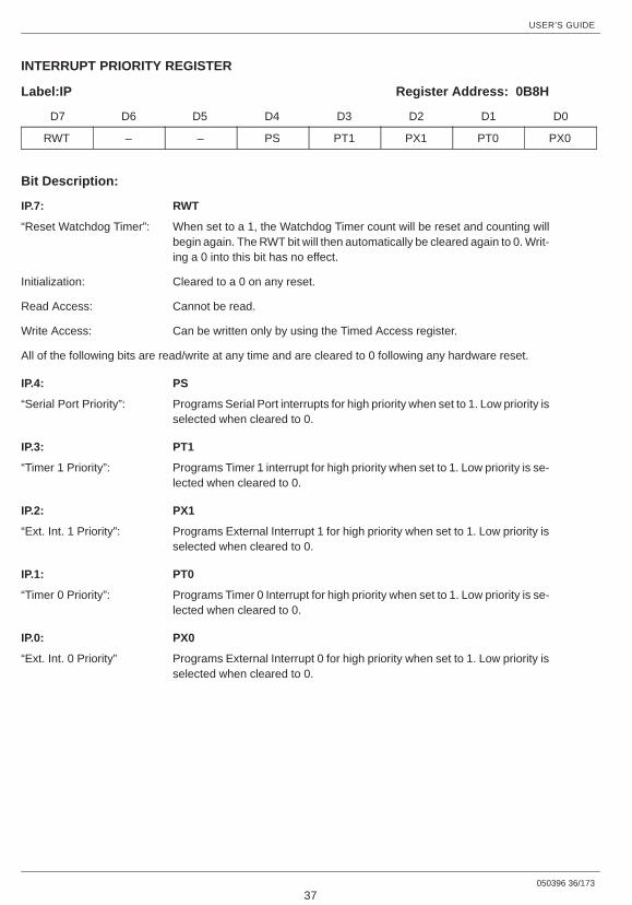
USER’S GUIDE
050396 36/173
37
INTERRUPT PRIORITY REGISTER
Label:IP Register Address: 0B8H
D7 D6 D5 D4 D3 D2 D1 D0
RWT – – PS PT1 PX1 PT0 PX0
Bit Description:
IP.7: RWT
“Reset Watchdog Timer”: When set to a 1, the Watchdog Timer count will be reset and counting willbegin again. The RWT bit will then automatically be cleared again to 0. Writ-ing a 0 into this bit has no effect.
Initialization: Cleared to a 0 on any reset.
Read Access: Cannot be read.
Write Access: Can be written only by using the Timed Access register.
All of the following bits are read/write at any time and are cleared to 0 following any hardware reset.
IP.4: PS
“Serial Port Priority”: Programs Serial Port interrupts for high priority when set to 1. Low priority isselected when cleared to 0.
IP.3: PT1
“Timer 1 Priority”: Programs Timer 1 interrupt for high priority when set to 1. Low priority is se-lected when cleared to 0.
IP.2: PX1
“Ext. Int. 1 Priority”: Programs External Interrupt 1 for high priority when set to 1. Low priority isselected when cleared to 0.
IP.1: PT0
“Timer 0 Priority”: Programs Timer 0 Interrupt for high priority when set to 1. Low priority is se-lected when cleared to 0.
IP.0: PX0
“Ext. Int. 0 Priority” Programs External Interrupt 0 for high priority when set to 1. Low priority isselected when cleared to 0.
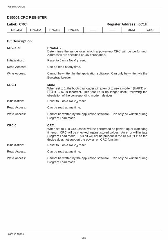
USER’S GUIDE
050396 37/173
38
DS5001 CRC REGISTER
Label: CRC Register Address: 0C1H
RNGE3 RNGE2 RNGE1 RNGE0 ––– ––– MDM CRC
Bit Description:
CRC.7–4 RNGE3–0Determines the range over which a power–up CRC will be performed.Addresses are specified on 4K boundaries.
Initialization: Reset to 0 on a No VLI reset.
Read Access: Can be read at any time.
Write Access: Cannot be written by the application software. Can only be written via theBootstrap Loader.
CRC.1 MDMWhen set to 1, the bootstrap loader will attempt to use a modem (UART) onPE4 if CRC is incorrect. This feature is no longer useful following theobsoletion of the corresponding modem devices.
Initialization: Reset to 0 on a No VLI reset.
Read Access: Can be read at any time.
Write Access: Cannot be written by the application software. Can only be written duringProgram Load mode.
CRC.0 CRCWhen set to 1, a CRC check will be performed on power–up or watchdogtimeout. CRC will be checked against stored values. An error will initiateProgram Load mode. This bit will not be present in the DS5002FP as thedevice does not support the power–on CRC function.
Initialization: Reset to 0 on a No VLI reset.
Read Access: Can be read at any time.
Write Access: Cannot be written by the application software. Can only be written duringProgram Load mode.
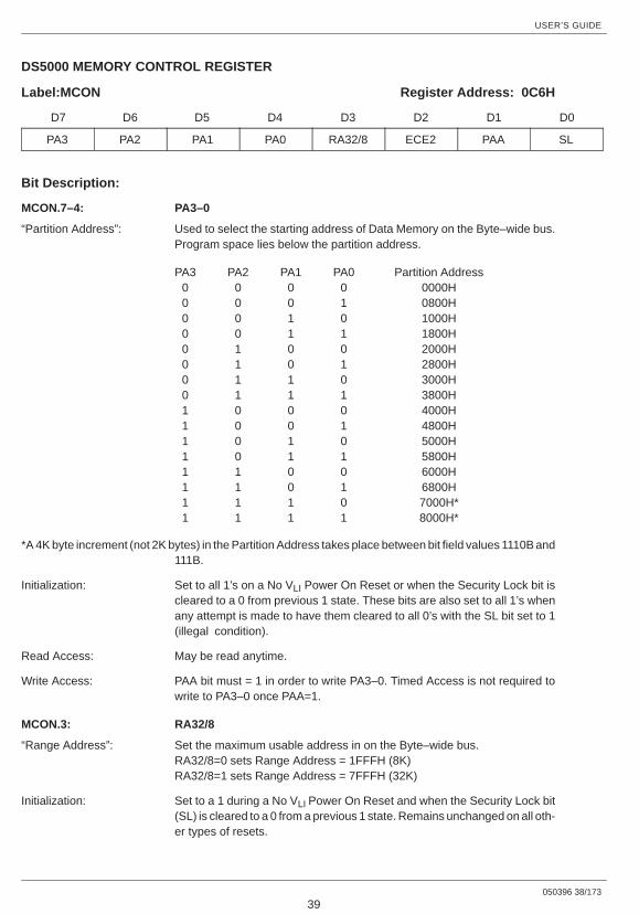
USER’S GUIDE
050396 38/173
39
DS5000 MEMORY CONTROL REGISTER
Label:MCON Register Address: 0C6H
D7 D6 D5 D4 D3 D2 D1 D0
PA3 PA2 PA1 PA0 RA32/8 ECE2 PAA SL
Bit Description:
MCON.7–4: PA3–0
“Partition Address”: Used to select the starting address of Data Memory on the Byte–wide bus.Program space lies below the partition address.
PA3 PA2 PA1 PA0 Partition Address0 0 0 0 0000H0 0 0 1 0800H0 0 1 0 1000H0 0 1 1 1800H0 1 0 0 2000H0 1 0 1 2800H0 1 1 0 3000H0 1 1 1 3800H1 0 0 0 4000H1 0 0 1 4800H1 0 1 0 5000H1 0 1 1 5800H1 1 0 0 6000H1 1 0 1 6800H1 1 1 0 7000H*1 1 1 1 8000H*
*A 4K byte increment (not 2K bytes) in the Partition Address takes place between bit field values 1110B and111B.
Initialization: Set to all 1’s on a No VLI Power On Reset or when the Security Lock bit iscleared to a 0 from previous 1 state. These bits are also set to all 1’s whenany attempt is made to have them cleared to all 0’s with the SL bit set to 1(illegal condition).
Read Access: May be read anytime.
Write Access: PAA bit must = 1 in order to write PA3–0. Timed Access is not required towrite to PA3–0 once PAA=1.
MCON.3: RA32/8
“Range Address”: Set the maximum usable address in on the Byte–wide bus.RA32/8=0 sets Range Address = 1FFFH (8K)RA32/8=1 sets Range Address = 7FFFH (32K)
Initialization: Set to a 1 during a No VLI Power On Reset and when the Security Lock bit(SL) is cleared to a 0 from a previous 1 state. Remains unchanged on all oth-er types of resets.
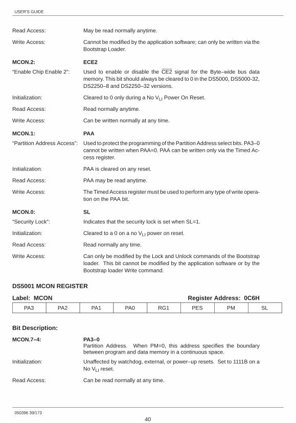
USER’S GUIDE
050396 39/173
40
Read Access: May be read normally anytime.
Write Access: Cannot be modified by the application software; can only be written via theBootstrap Loader.
MCON.2: ECE2
“Enable Chip Enable 2”: Used to enable or disable the CE2 signal for the Byte–wide bus datamemory. This bit should always be cleared to 0 in the DS5000, DS5000-32,DS2250–8 and DS2250–32 versions.
Initialization: Cleared to 0 only during a No VLI Power On Reset.
Read Access: Read normally anytime.
Write Access: Can be written normally at any time.
MCON.1: PAA
“Partition Address Access”: Used to protect the programming of the Partition Address select bits. PA3–0cannot be written when PAA=0. PAA can be written only via the Timed Ac-cess register.
Initialization: PAA is cleared on any reset.
Read Access: PAA may be read anytime.
Write Access: The Timed Access register must be used to perform any type of write opera-tion on the PAA bit.
MCON.0: SL
“Security Lock”: Indicates that the security lock is set when SL=1.
Initialization: Cleared to a 0 on a no VLI power on reset.
Read Access: Read normally any time.
Write Access: Can only be modified by the Lock and Unlock commands of the Bootstraploader. This bit cannot be modified by the application software or by theBootstrap loader Write command.
DS5001 MCON REGISTER
Label: MCON Register Address: 0C6H
PA3 PA2 PA1 PA0 RG1 PES PM SL
Bit Description:
MCON.7–4: PA3–0Partition Address. When PM=0, this address specifies the boundarybetween program and data memory in a continuous space.
Initialization: Unaffected by watchdog, external, or power–up resets. Set to 1111B on aNo VLI reset.
Read Access: Can be read normally at any time.
USER’S GUIDE
050396 40/173
41
Write Access: Timed Access Protected. Cannot be written by the application software ifset to 0000B by the serial loader. If a 0000B is written via the serial loaderand the security lock is set, the Partition will become 1111B. The same willoccur if write access is available and application software writes a 0000B. Inaddition, these bits will be set to 1111B if security lock is cleared.
MCON.3: RG1One of two bits that determine the range of program space. RG0 is locatedin the RPCTL register.
Initialization: Unaffected by watchdog, external, or power–up resets. Set to 1 on a No VLIreset or a clearing of the security lock.
Read Access: Can be read at any time.
Write Access: Cannot be modified by the application software. Can only be written via theBootstrap Loader.
MCON.2: PESPeripheral Enable Select. When this bit is set, the data space is controlledby PE1–PE4. Peripherals are memory–mapped in 16K blocks, and areaccessed by MOVX instructions on the Byte–wide bus.
Initialization: Cleared by all resets.
Read Access: Can be read at any time.
Write Access: Can be written at any time.
MCON.1: PMPartition Mode. When PM=0, a partitionable, continuous memory map isinvoked. When PM=1, one of four fixed allocations is used.
Initialization: Unaffected by watchdog, external, or power–up resets. Cleared on a No VLIreset.
Read Access: Can be read at any time.
Write Access: Cannot be modified by the application software. Can only be modified viathe Boostrap Loader.
MCON.0: SL
“Security Lock”: Indicates that the security lock is set when SL=1.
Initialization: Cleared to a 0 on a no VLI power on reset.
Read Access: Read normally any time.
Write Access: Can only be modified by the Lock and Unlock commands of the Bootstraploader. This bit cannot be modified by the application software or by theBootstrap loader Write command.
USER’S GUIDE
050396 41/173
42
PROGRAM STATUS WORD REGISTER
Label:PSW Register Address: 0D0H
D7 D6 D5 D4 D3 D2 D1 D0
C AC F0 RS1 RS0 OV P
All of the bits in PSW except parity are read/write and are cleared to 0 on any type of reset. The Parity bit is read onlyand is cleared to 0 on any type of reset.
Bit Description:
PSW.7: C
“Carry”: Set when the previous operation resulted in a carry (during addition) or aborrow (during subtraction). Otherwise cleared.
PSW.6: AC
“Auxiliary-Carry”: Set when the previous operation resulted in a carry (during addition) or aborrow (during subtraction) from the low–order nibble. Otherwise cleared.
PSW.5: F0
“User Flag 0”: General–purpose flag bit which can be set or cleared as needed.
PSW.4–3: R1–R0
“Register Bank Select”: Used to select an 8–byte bank of registers within the Data Register space tobe assigned as R0–R8 in subsequent instructions. The 8–byte bank startingaddress selection is as follows:
R1 R0 Data Register Address (R0)0 0 00H0 1 08H1 0 10H1 1 18H
PSW.2: OV
“Overflow”: Set when a carry was generated into the high–order bit but not a carry out ofthe high–order bit as a result of the previous operation, and visa–versa. OVis normally used in 2’s complement arithmetic.
PSW.0: P
“Parity”: Set if the modulo–2 sum of the eight bits of the accumulator is 1 (odd parity);cleared on even parity.

USER’S GUIDE
050396 42/173
43
DS5001/DS5002 RPC CONTROL REGISTER
Label: RPCTL Register Address: 0D8H
RNR ––– EXBS AE IBI DMA RPCON RG0
Bit Description:
RPCTL.7 RNRWhen internal hardware sets this read–only bit to a 1, a new value may beread from the random number generator register of the DS5001/DS5002(RNR;0CFh). This bit is cleared when the random number is read, andapproximately 160 µs are required to generated the next number.
Initialization: Cleared after all resets. Bit will be set approximately 160 µsec after a reset.
Read Access: Can be read at any time.
Write Access: Cannot be written.
RPCTL.5 EXBSThe Expanded Bus Select routes data memory access (MOVX) to theexpanded bus formed by ports 0 and 2 when set.
Initialization: Cleared after all resets.
Read Access: Can be read at any time.
Write Access: Can be written at any time.
RPCTL.4 AEAccess Enable is used when a software reload is desired without using theBootstrap Loader. When set, the device will be temporarily configured in aPartitionable configuration with the Partition at 4K. This will occur even if thePM=1. When cleared, the prior memory configuration is resumed.
Initialization: Cleared after all resets.
Read Access: Can be read at any time.
Write Access: Can be written at any time, Timed Access protected.
RPCTL.3 IBIWhen using the RPC mode, an interrupt may be required for the InputBuffer Flag. This interrupt is enabled by setting the Input Buffer Interrupt(IBI) bit. At this time, the timer 1 interrupt is disabled, and this RPC modeinterrupt is used in its place (vector location 1BH). This bit can be set onlywhen the RPCON bit is set.
Initialization: Cleared on all resets, and when the RPCON bit is cleared.
Read Access: Can be read at any time.
Write Access: Can be written when the RPC mode is enabled (RPCON=1).
RPCTL.2 DMAThis bit is set to enable DMA transfers when RPC mode is invoked. It canonly be set when RPCON=1.
Initialization: Cleared on all resets, and when RPC is cleared.

USER’S GUIDE
050396 43/173
44
Read Access: Can be read anytime.
Write Access: Can be written when the RPC mode is enabled (RPCON=1).
RPCTL.1 RPCONEnable the RPC 8042 I/O protocol. When set, port 0 becomes the data bus,and port 2 becomes the control signals.
Initialization: Cleared on all resets.
Read Access: Can be read at any time.
Write Access: Can be written at any time.
RPCTL.0 RG0This is a Range bit which is used to determine the size of the programmemory space. Its usage is shown above.
Initialization: Unaffected by watchdog, external, or power–up resets. Cleared on a No VLIreset or clearing of the security lock.
Read Access: Can be read at any time.
Write Access: Cannot be modified by the application software. Can only be modified viathe Bootstrap loader.
DS5001/DS5002 RPC STATUS REGISTER
Label: RPS Register Address: 0DAH
ST7 ST6 ST5 ST4 IA0 F0 IBF OBF
Bit Description:
RPS.7–4: General purpose status bits that can be written by the microcontroller andcan be read by the external host.
Initialization: Cleared when RPCON=0.
Read Access: Can be read by DS5001/DS5002 and host CPU when RPC mode is invoked.
Write Access: Can be written by the DS5001/DS5002 when RPC mode is invoked.
RPS.3: IA0Stores the value of the external system A0 for the last DBBIN Write whena valid write occurs (as determined by the IBF flag).
Initialization: Cleared when RPC=0.
Read Access: Can be read by DS5001/DS5002 and host CPU when in RPC mode.
Write Access: Automatically written when a valid DBBIN Write occurs. Cannot be writtenotherwise.
RPS.2: F0General purpose flag written by the DS5001/DS5002 and read by theexternal host.
Initialization: Cleared when RPC=0.

USER’S GUIDE
050396 44/173
45
Read Access: Can be read by DS5001/DS5002 and host CPU when in RPC mode.
Write Access: Can be written by the DS5001/DS5002 when in RPC mode.
RPS.1: IBFInput Buffer Full Flag is set following a write by the external host, and iscleared following a read of the DBBIN by the DS5001/DS5002.
Initialization: Cleared when RPC=0.
Read Access: Can be read by DS5001/DS5002 and host CPU when in RPC mode.
Write Access: Written automatically as part of the RPC communication. Cannot be set bythe application software.
RPS.0: OBFOutput Buffer Full Flag is set following a write of the DBBOUT by theDS5001/DS5002, and is cleared following a read of the DBBOUT by theexternal host.
Initialization: Cleared when RPC=0.
Read Access: Can be read by DS5001/DS5002 and host CPU when in RPC mode.
Write Access: Written automatically as part of the RPC communication. Cannot be set bythe application software.

USER’S GUIDE
050396 45/173
46
INSTRUCTION SETIntroductionThe Secure Microcontroller executes an instruction setwhich is object code compatible with the industry stan-dard 8051 microcontroller. As a result, software toolswritten for the 8051 are compatible with the SecureMicrocontroller, including cross–assemblers, compil-ers, and debugging tools.
There are a total of 42 instruction types recognized bythe Secure Microcontroller. When the instruction usesboth source and destination operands, they are speci-fied in the order of “destination, source”.
Addressing ModesThere are eight addressing modes. Five of these areused to address operands. The other three are used ininstructions which transfer execution of the program toanother address (e.g., Branch, Jump, Call).
The modes which address source operands, includeRegister Addressing, Direct Addressing, Register–Indi-rect Addressing, Immediate Addressing and Register-Indirect with Displacement. The first three of these canalso be used to address a destination operand. Mostinstructions use operands that are located in the InternalData Registers.
The addressing modes used for the Control Transferinstructions include Relative Addressing, Page Addres-sing, and Extended Addressing.
The operation of these addressing modes is summa-rized below, followed by an example.
Register AddressingRegister Addressing is used on operands contained inone of the eight registers (R7–R0) of the currently se-lected Working Register Bank. A register bank is se-lected via a 2–bit field in the PSW Special Function reg-ister. All of the Working registers may also be accessedthrough either Direct Addressing or Register-IndirectAddressing as well. This is due to the fact that the Work-ing registers are mapped into the lower 32 bytes of Inter-nal Data RAM as discussed above.
ADD A, R4 ; Add Accumulator to Working ; register R4
Direct AddressingDirect Addressing is the only mode available for use onoperands within the Special Function registers. Ad-dressing of bytes may also be used to access the 128Internal Data registers.
MOV 072H, 074H ; Load direct register (addr. 072H); with direct register (074H)
Direct addressing of bits is available on 128 bits locatedin the Internal Data registers in byte addresses of 20H –2FH inclusive. Direct bit addressing is also available inSpecial Function registers located at addresses on8–byte boundaries starting at 80H (i.e., 80H, 88H, 90H,98H, ...0F0H, 0F8H).
SETB 00H ; Set addressable bit 00H (D0 in ; Internal Data Reg. 20H)
Register Indirect AddressingSome instructions use Register–Indirect Addressing foraccessing operands in other Internal Data registers.This is done by using the contents of Working registerR1 or R0 as a pointer to other Internal Data registers.
ANL A, @R0 ; Logical AND of Accumulator with ; Internal Data register; pointed to ; by contents of R0
In addition, this addressing is used via the Stack Pointerregister (SP) for manipulation of the stack. The stackarea is contained in the Internal Data Register area. ThePUSH and POP instructions are the only ones whichuse SP for this addressing mode.
PUSH P0 ; Save the contents of the Port 0 ; SFR latch on the stack
The R0, R1, and the DPTR registers are used with Reg-ister–Indirect Addressing for accessing Data Memory.R1 or R0 in the selected Working Register bank may beused for accessing location within a 256–byte blockpointed to by the current contents of the P2 SFR latch(address high byte).
MOVX A, @R1 ; Load the Accumulator with the ; contents of Data Memory ; addressed by the 8–bit contents; of R1

USER’S GUIDE
050396 46/173
47
The 16–bit DPTR register may be used to access anyData Memory location within the 64K byte space.
MOVX @DPTR,A ; Load the Data Memory location ; pointed to by the contents of the ; DPTR register with the contents ; of the Accumulator.
Immediate AddressingImmediate Addressing is used to access constants foruse as operands which are contained in the currentinstruction in Program Memory.
ORL A, #040H ; Logical OR of the Accumulator ; with the constant value of 040H
Register–Indirect with DisplacementRegister–Indirect with Displacement Addressing isused to access data in look–up tables in ProgramMemory space. The location accessed is pointed to bythe contents of either the DPTR or the PC registers,which are used as a base register added together withthe contents of the Accumulator (A), which is used as anindex register.
MOVC A, @DPTR+A ; Load the Accumulator with ; the contents of the Program ; Memory location pointed to ; by the value of the DPTR ; register plus the value ; contained in the Accumulator
Relative AddressingRelative Addressing is used in the determination of adestination address for the Conditional Branch instruc-tions. Each of these instructions includes an 8–bit bytewhich contains a 2’s complement address offset (–127
to +128) which is added to the PC to determine the des-tination address which will be branched to when thetested condition is found to be true. The PC points to theProgram Memory location immediately after the Branchinstruction when the offset is added. If the condition isfound to be not true, then program execution continuesfrom the address of the following instruction.
JZ –20 ; Branch to the location (PC+2) –20 ; if the contents of the Accumulator
; = 0
Page AddressingPage Addressing is used by the Control Transferinstructions to specify a destination address within the2K byte block in which the next contiguous instructionresides. The full 16–bit address is calculated by takingthe highest-order five bits for the next contiguousinstruction (PC+2) and concatenating them with thelowest-order 11–bit filed contained in the currentinstruction. 11–bit field provides an efficient instructionencoding of a destination address for these instructions.
0830 ACALL 100H ; Call to the subroutine at ; address 0100H + current ; page address
In this case the destination address would be 800H +100H or 900H.
Extended AddressingExtended Addressing is used in the Control TransferInstructions to specify a 16–bit destination addresswithin the entire 64K byte addressable range of theSecure Microcontroller.
LJMP 0FF80H ; Jump to address 0FF80H
USER’S GUIDE
050396 47/173
48
Program Status FlagsAll of the Program Status flags are contained in the PSWregister. Instructions which affect the states of the flagsare summarized below.
INSTRUCTIONS THAT AFFECT FLAG SETTINGS
INSTRUCTION
FLAGS
C OV AC INSTRUCTION
FLAGS
C OV AC
ADD � � � CLR C 0
ADDC � � � CPL C �
SUBB � � � ANL C, bit �
MUL 0 � ANL C, bit �
DIV 0 � ORL C, bit �
DA � ORL C, bit �
RRC � MOV C, bit �
RLC � CJNE �
SETB C 1
LEGEND:0 = Cleared to 01 = Set to a 1� = Modified according to the result of the operation.
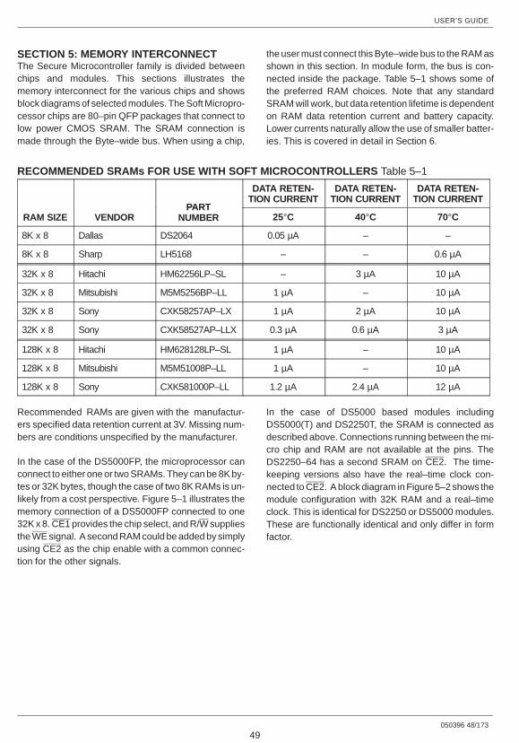
USER’S GUIDE
050396 48/173
49
SECTION 5: MEMORY INTERCONNECTThe Secure Microcontroller family is divided betweenchips and modules. This sections illustrates thememory interconnect for the various chips and showsblock diagrams of selected modules. The Soft Micropro-cessor chips are 80–pin QFP packages that connect tolow power CMOS SRAM. The SRAM connection ismade through the Byte–wide bus. When using a chip,
the user must connect this Byte–wide bus to the RAM asshown in this section. In module form, the bus is con-nected inside the package. Table 5–1 shows some ofthe preferred RAM choices. Note that any standardSRAM will work, but data retention lifetime is dependenton RAM data retention current and battery capacity.Lower currents naturally allow the use of smaller batter-ies. This is covered in detail in Section 6.
RECOMMENDED SRAMs FOR USE WITH SOFT MICROCONTROLLERS Table 5–1
PART
DATA RETEN-TION CURRENT
DATA RETEN-TION CURRENT
DATA RETEN-TION CURRENT
RAM SIZE VENDORPART
NUMBER 25°C 40°C 70°C
8K x 8 Dallas DS2064 0.05 µA – –
8K x 8 Sharp LH5168 – – 0.6 µA
32K x 8 Hitachi HM62256LP–SL – 3 µA 10 µA
32K x 8 Mitsubishi M5M5256BP–LL 1 µA – 10 µA
32K x 8 Sony CXK58257AP–LX 1 µA 2 µA 10 µA
32K x 8 Sony CXK58527AP–LLX 0.3 µA 0.6 µA 3 µA
128K x 8 Hitachi HM628128LP–SL 1 µA – 10 µA
128K x 8 Mitsubishi M5M51008P–LL 1 µA – 10 µA
128K x 8 Sony CXK581000P–LL 1.2 µA 2.4 µA 12 µA
Recommended RAMs are given with the manufactur-ers specified data retention current at 3V. Missing num-bers are conditions unspecified by the manufacturer.
In the case of the DS5000FP, the microprocessor canconnect to either one or two SRAMs. They can be 8K by-tes or 32K bytes, though the case of two 8K RAMs is un-likely from a cost perspective. Figure 5–1 illustrates thememory connection of a DS5000FP connected to one32K x 8. CE1 provides the chip select, and R/W suppliesthe WE signal. A second RAM could be added by simplyusing CE2 as the chip enable with a common connec-tion for the other signals.
In the case of DS5000 based modules includingDS5000(T) and DS2250T, the SRAM is connected asdescribed above. Connections running between the mi-cro chip and RAM are not available at the pins. TheDS2250–64 has a second SRAM on CE2. The time-keeping versions also have the real–time clock con-nected to CE2. A block diagram in Figure 5–2 shows themodule configuration with 32K RAM and a real–timeclock. This is identical for DS2250 or DS5000 modules.These are functionally identical and only differ in formfactor.
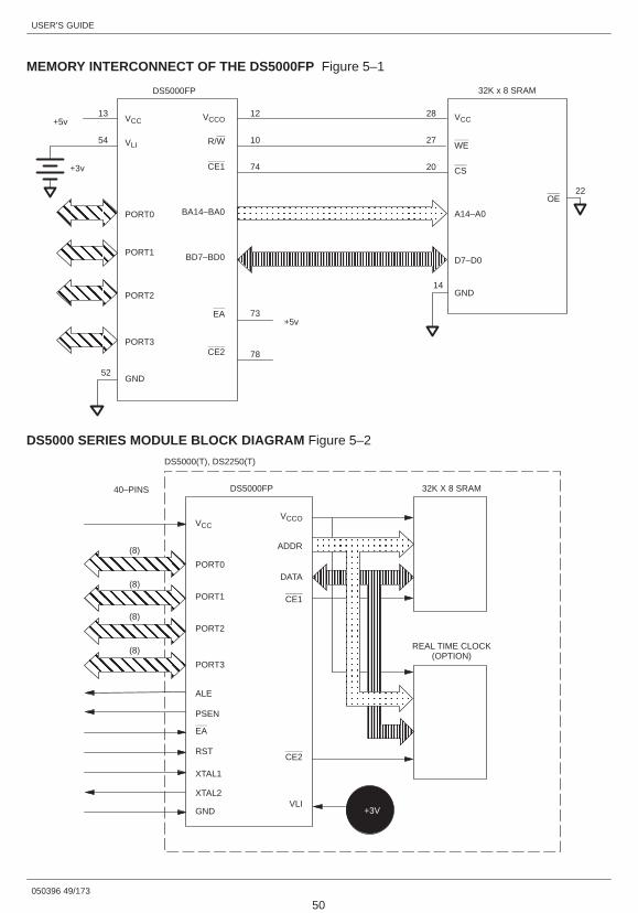
ÇÇÇÇÇÇ
ÇÇÇÇÇÇÇÇÇÇ ÇÇ
ÇÇÇÇÇÇÇÇÇÇÇÇÇÇ ÇÇ
ÇÇÇÇ
ÇÇÇÇÇÇÇÇÇÇ ÇÇ
ÇÇÇÇÇÇÇÇÇÇÇÇÇÇ
ÔÔÔÔÔÔÔÔÔÔÔÔÔÔÔÔÔÔÔÔÔÔÔÔÔÔÔÔÔÔÔÔÔÔÔÔÔÔÔÔÔÔÔÔÔÔÔÔÔÔÔÔÔÔ
ÓÓÓÓÓÓÓÓÓÓÓÓÓÓÓÓÓÓÓÓÓÓÓÓÓÓÓÓÓÓÓÓÓÓÓÓÓÓÓÓÓÓÓÓÓÓÓÓÓÓÓÓÓÓ
REAL TIME CLOCK(OPTION)
32K X 8 SRAMDS5000FP
DS5000(T), DS2250(T)
40–PINS
(8)
(8)
(8)
(8)
VCC
PORT0
PORT1
PORT2
PORT3
ALE
PSEN
EA
RST
XTAL1
XTAL2
GND
VCCO
ADDR
DATA
CE1
CE2
VLI+3V
USER’S GUIDE
050396 49/173
50
MEMORY INTERCONNECT OF THE DS5000FP Figure 5–1
ÓÓ
ÓÓÓÓÓÓÓÓÓÓÓÓÓÓÓÓÓÓÓÓ
ÔÔ
ÔÔÔÔÔÔÔÔÔÔÔÔÔÔÔÔÔÔÔÔÔÔ
ÇÇÇÇÇÇÇÇÇÇÇ
ÇÇÇÇÇÇÇÇÇÇÇ
ÇÇÇÇÇÇÇÇÇÇ
ÇÇÇÇÇÇÇÇÇÇ
13
54
+3v
+5v12
10
74
28
27
20
22
14
73
78
+5v
52
DS5000FP
VCC
WE
CS
A14–A0
D7–D0
GND
OE
32K x 8 SRAM
VCCO
R/W
CE1
BA14–BA0
BD7–BD0
EA
CE2
VCC
VLI
PORT0
PORT1
PORT2
PORT3
GND
DS5000 SERIES MODULE BLOCK DIAGRAM Figure 5–2
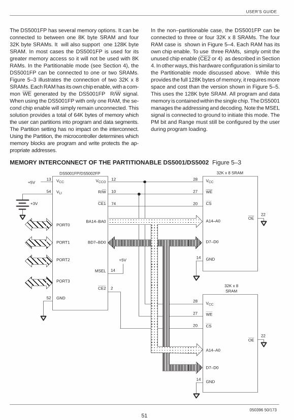
ÇÇ
ÇÇÇÇÇÇÇÇ
ÇÇ
ÇÇÇÇÇÇÇÇ
ÇÇ
ÇÇÇÇÇÇÇÇ
ÇÇ
ÇÇÇÇÇÇÇÇ
VCCO
R/W
CE1
BA14–BA0
BD7–BD0
MSEL
CE2
VCC
VLI
PORT0
PORT1
PORT2
PORT3
GND
28
27
20
14
VCC
WE
CS
A14–A0
D7–D0
GND
OE
32K x 8 SRAM
VCC
WE
CS
A14–A0
D7–D0
GND
OE
32K x 8SRAM
ÔÔÔÔÔÔÔÔÔÔÔÔÔÔÔÔÔÔÔÔÔÔÔÔÔÔÔÔÔÔÔÔÔÔÔÔÔÔÔÔÔÔÔÔÔÔÔÔÔÔÔÔÔÔÔÔÔÔÔÔÔÔÔÔÔÔÔÔÔÔÔÔÔÔÔÔÔÔÔÔÔÔÔÔÔÔÔÔÔÔÔÔÔÔÔÔÔÔÔÔÔÔÔÔÔÔÔÔÔÔÔÔÔÔÔÔÔÔÔÔÔÔÔÔÔÔÔÔÔÔÔÔÔÔÔÔÔÔÔÔ
ÓÓÓÓÓÓÓÓÓÓÓÓÓÓÓÓÓÓÓÓÓÓÓÓÓÓÓÓÓÓÓÓÓÓÓÓÓÓÓÓÓÓÓÓÓÓÓÓÓÓÓÓÓÓÓÓÓÓÓÓÓÓÓÓÓÓÓÓÓÓÓÓÓÓÓÓÓÓÓÓÓÓÓÓÓÓÓÓÓÓÓÓÓÓÓÓÓÓÓÓÓÓÓÓÓÓÓÓÓÓÓÓÓÓÓÓÓÓÓÓÓÓÓÓÓÓÓÓÓÓÓÓÓÓÓÓÓÓÓÓ
28
27
20
14
VCC
WE
CS
A14–A0
D7–D0
GND
OE
32K x 8SRAM
22
22
+5V
14
2
12
10
74
13
54
+3V
+5V
52
DS5001FP/DS5002FP
USER’S GUIDE
050396 50/173
51
The DS5001FP has several memory options. It can beconnected to between one 8K byte SRAM and four32K byte SRAMs. It will also support one 128K byteSRAM. In most cases the DS5001FP is used for itsgreater memory access so it will not be used with 8KRAMs. In the Partitionable mode (see Section 4), theDS5001FP can be connected to one or two SRAMs.Figure 5–3 illustrates the connection of two 32K x 8SRAMs. Each RAM has its own chip enable, with a com-mon WE generated by the DS5001FP R/W signal.When using the DS5001FP with only one RAM, the se-cond chip enable will simply remain unconnected. Thissolution provides a total of 64K bytes of memory whichthe user can partitions into program and data segments.The Partition setting has no impact on the interconnect.Using the Partition, the microcontroller determines whichmemory blocks are program and write protects the ap-propriate addresses.
In the non–partitionable case, the DS5001FP can beconnected to three or four 32K x 8 SRAMs. The fourRAM case is shown in Figure 5–4. Each RAM has itsown chip enable. To use three RAMs, simply omit theunused chip enable (CE2 or 4) as described in Section4. In other ways, this hardware configuration is similar tothe Partitionable mode discussed above. While thisprovides the full 128K bytes of memory, it requires morespace and cost than the version shown in Figure 5–5.This uses the 128K byte SRAM. All program and datamemory is contained within the single chip. The DS5001manages the addressing and decoding. Note the MSELsignal is connected to ground to initiate this mode. ThePM bit and Range must still be configured by the userduring program loading.
MEMORY INTERCONNECT OF THE PARTITIONABLE DS5001/DS5002 Figure 5–3
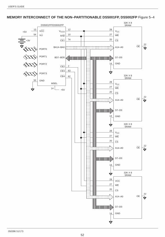
ÇÇÇÇÇÇÇÇÇÇÇÇÇÇÇÇÇÇ
ÇÇÇÇÇÇÇÇÇÇÇÇÇÇÇÇÇÇÇÇÇÇÇÇÇÇ
ÔÔÔÔÔÔÔÔÔÔÔÔÔÔÔÔÔÔÔÔÔÔÔÔÔÔÔÔÔÔÔÔÔÔÔÔÔÔÔÔÔÔÔÔÔÔÔÔÔÔÔÔÔÔÔÔÔÔÔÔÔÔÔÔÔÔÔÔÔÔÔÔÔÔÔÔÔÔÔÔÔÔÔÔÔÔÔÔÔÔÔÔÔÔÔÔÔÔÔÔÔÔÔÔÔÔÔÔÔÔÔÔÔÔÔÔÔÔÔÔÔÔÔÔÔÔÔÔÔÔÔÔÔÔÔÔÔÔÔÔÔÔÔÔÔÔÔÔÔÔÔÔÔÔÔÔÔÔÔÔÔÔÔÔÔÔÔÔÔÔÔÔÔÔÔÔÔÔÔÔÔÔÔÔÔÔÔÔÔÔÔÔÔÔÔÔÔÔÔÔÔÔÔÔÔÔÔÔÔÔÔÔÔÔÔÔÔÔÔÔÔÔÔÔÔÔÔÔÔÔÔÔÔÔÔÔÔÔÔÔÔÔÔÔÔÔÔÔÔÔÔÔ
ÓÓÓÓÓÓÓÓÓÓÓÓÓÓÓÓÓÓÓÓÓÓÓÓÓÓÓÓÓÓÓÓÓÓÓÓÓÓÓÓÓÓÓÓÓÓÓÓÓÓÓÓÓÓÓÓÓÓÓÓÓÓÓÓÓÓÓÓÓÓÓÓÓÓÓÓÓÓÓÓÓÓÓÓÓÓÓÓÓÓÓÓÓÓÓÓÓÓÓÓÓÓÓÓÓÓÓÓÓÓÓÓÓÓÓÓÓÓÓÓÓÓÓÓÓÓÓÓÓÓÓÓÓÓÓÓÓÓÓÓÓÓÓÓÓÓÓÓÓÓÓÓÓÓÓÓÓÓÓÓÓÓÓÓÓÓÓÓÓÓÓÓÓÓÓÓÓÓÓÓÓÓÓÓÓÓÓÓÓÓÓÓÓÓÓÓÓÓÓÓÓÓÓÓÓÓÓÓÓÓÓÓÓÓÓÓÓÓÓÓÓÓÓÓÓÓÓÓÓÓÓÓÓÓÓÓÓÓÓÓÓÓÓ
28
27
20
14
28
27
20
14
28
27
20
14
28
27
20
14
22
22
22
22
12
10
74
2
63
62
14+5V
13
54
+3V
52
DS5001FP/DS5002FP
+5V VCC
VLI
PORT0
PORT1
PORT2
PORT3
GND
VCCO
R/W
CE1
BA14–BA0
BD7–BD0
CE2
CE3
CE4
MSEL
VCC
WE
CS
A14–A0
D7–D0
GND
OE
32K X 8SRAM
VCC
WE
CS
A14–A0
D7–D0
GND
OE
32K X 8SRAM
VCC
WE
CS
A14–A0
D7–D0
GND
OE
32K X 8SRAM
VCC
WE
CS
A14–A0
D7–D0
GND
OE
32K X 8SRAM
USER’S GUIDE
050396 51/173
52
MEMORY INTERCONNECT OF THE NON–PARTITIONABLE DS5001FP, DS5002FP Figure 5–4
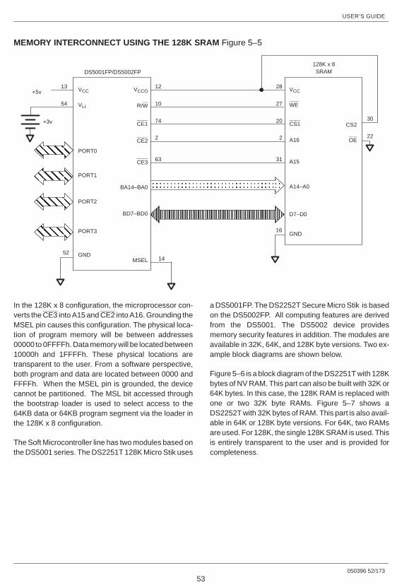
USER’S GUIDE
050396 52/173
53
MEMORY INTERCONNECT USING THE 128K SRAM Figure 5–5
ÓÓÓÓÓÓÓÓÓÓÓÓÓÔÔÔÔÔÔÔÔÔÔÔÔÔ
ÔÔÇ
ÇÇ
ÇÇÇÇÇÇ
ÇÇÇ
ÇÇÇÇÇÇ
ÇÇ
ÇÇÇÇÇ
ÇÇ
ÇÇÇÇÇÇÇÇ
13
54
+3v
+5v12
10
74
28
27
20
22
16
1452
DS5001FP/DS5002FP
VCC
WE
CS1
A16
A15
A14–A0
D7–D0
GND
CS2
OE
128K x 8SRAM
VCCO
R/W
CE1
CE2
CE3
BA14–BA0
BD7–BD0
MSEL
VCC
VLI
PORT0
PORT1
PORT2
PORT3
GND
2
63
30
2
31
In the 128K x 8 configuration, the microprocessor con-verts the CE3 into A15 and CE2 into A16. Grounding theMSEL pin causes this configuration. The physical loca-tion of program memory will be between addresses00000 to 0FFFFh. Data memory will be located between10000h and 1FFFFh. These physical locations aretransparent to the user. From a software perspective,both program and data are located between 0000 andFFFFh. When the MSEL pin is grounded, the devicecannot be partitioned. The MSL bit accessed throughthe bootstrap loader is used to select access to the64KB data or 64KB program segment via the loader inthe 128K x 8 configuration.
The Soft Microcontroller line has two modules based onthe DS5001 series. The DS2251T 128K Micro Stik uses
a DS5001FP. The DS2252T Secure Micro Stik is basedon the DS5002FP. All computing features are derivedfrom the DS5001. The DS5002 device providesmemory security features in addition. The modules areavailable in 32K, 64K, and 128K byte versions. Two ex-ample block diagrams are shown below.
Figure 5–6 is a block diagram of the DS2251T with 128Kbytes of NV RAM. This part can also be built with 32K or64K bytes. In this case, the 128K RAM is replaced withone or two 32K byte RAMs. Figure 5–7 shows aDS2252T with 32K bytes of RAM. This part is also avail-able in 64K or 128K byte versions. For 64K, two RAMsare used. For 128K, the single 128K SRAM is used. Thisis entirely transparent to the user and is provided forcompleteness.

USER’S GUIDE
050396 53/173
54
DS2251T–128 BLOCK DIAGRAM Figure 5–6
ÇÇÇ
ÇÇÇÇÇÇÇÇ Ç
ÇÇÇÇÇÇÇÇÇÇÇÇÇ Ç
ÇÇ
ÇÇÇÇÇÇÇÇ Ç
ÇÇÇÇÇÇÇÇÇÇÇÇÇ
ÔÔÔÔÔÔÔÔÔÔÔÔÔÔÔÔÔÔÔÔÔÔÔÔÔÔÔÔÔÔÔÔÔÔÔÔÔÔÔÔÔÔÔÔÔÔÔÔÔÔÔÔÔÔÔÔÔÔÔÔÔÔÔÔÔÔÔÔÔÔÔÔÔÔÔÔÔÔÔÔÔÔÔÔÔÔÔÔÔÔÔÔÔÔÔÔÔÔÔÔÔÔÔÔÔÔÔÔÔÔÔÔÔÔÔÔÔÔÔÔÔÔÔÔÔÔÔÔÔÔÔÔÔÔÔÔÔÔÔÔÔÔÔÔÔÔÔÔÔÔÔÔÔÔÔÔÔÔÔÔÔÔÔÔÔÔÔÔÔÔÔÔÔÔÔÔÔÔÔÔÔÔÔÔÔÔÔÔÔÔÔÔÔÔÔÔÔÔÔÔÔÔÔÔÔÔÔÔÔÔÔÔÔÔÔÔÔÔÔÔÔÔÔÔÔÔÔÔÔÔÔÔÔÔÔÔÔÔÔÔÔÔÔÔÔÔÔÔÔÔÔÔÔÔÔÔÔÔÔÔÔÔÔÔÔÔÔÔÔÔÔÔÔÔÔÔÔÔÔÔÔÔÔÔÔÔÔÔÔÔÔÔÔÔÔÔÔÔÔÔÔÔÔÔÔÔÔÔÔÔÔÔÔÔÔÔÔÔÔÔÔÔÔÔÔÔÔÔÔÔÔÔÔÔÔÔÔÔÔÔÔÔÔÔÔÔÔÔÔÔÔÔÔÔÔÔÔÔÔÔÔÔÔÔÔÔÔÔÔÔÔÔÔÔÔÔÔÔÔÔÔÔÔÔÔÔÔÔÔÔÔ
ÓÓÓÓÓÓÓÓÓÓÓÓÓÓÓÓÓÓÓÓÓÓÓÓÓÓÓÓÓÓÓÓÓÓÓÓÓÓÓÓÓÓÓÓÓÓÓÓÓÓÓÓÓÓÓÓÓÓÓÓÓÓÓÓÓÓÓÓÓÓÓÓÓÓÓÓÓÓÓÓÓÓÓÓÓÓÓÓÓÓÓÓÓÓÓÓÓÓÓÓÓÓÓÓÓÓÓÓÓÓÓÓÓÓÓÓÓÓÓÓÓÓÓÓÓÓÓÓÓÓÓÓÓÓÓÓÓÓÓÓÓÓÓÓÓÓÓÓÓÓÓÓÓÓÓÓÓÓÓÓÓÓÓÓÓÓÓÓÓÓÓÓÓÓÓÓÓÓÓÓÓÓÓÓÓÓÓÓÓÓÓÓÓÓÓÓÓÓÓÓÓÓÓÓÓÓÓÓÓÓÓÓÓÓÓÓÓÓÓÓÓÓÓÓÓÓÓÓÓÓÓÓÓÓÓÓÓÓÓÓÓÓÓÓÓÓÓÓÓÓÓÓÓÓÓÓÓÓÓÓÓÓÓÓÓÓÓÓÓÓÓÓÓÓÓÓÓÓÓÓÓÓÓÓÓÓÓÓÓÓÓÓÓÓÓÓÓÓÓÓÓÓÓÓÓÓÓÓÓÓÓÓÓÓÓÓÓÓÓÓÓÓÓÓÓÓÓÓÓÓÓÓÓÓÓÓÓÓÓÓÓÓÓÓÓÓÓÓÓÓÓÓÓÓÓÓÓÓÓÓÓÓÓÓÓÓÓÓÓÓÓÓÓÓÓÓÓÓÓÓÓÓÓÓÓÓÓÓÓÓÓ
DS2251T
DS5001FP 128K X 8 SRAM
REAL TIME CLOCK
BYTE–WIDE ADDRESS BUS
BYTE–WIDE DATA BUS
(14)
(8)
(8)
(8)
(8)
(8)
R/W
INTA
INTB
INTP
SQW
+3V
VLI
VCC
PORT0
PORT1
PORT2
PORT3
ALE
RST
PSEN
PROG
PF
VRST
PE3
PE4
XTAL1
XTAL2
GND
VCCO
ADDR
R/W
DATA
CE1
PE1
72 PINS
DS1283
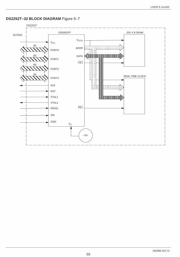
USER’S GUIDE
050396 54/173
55
DS2252T–32 BLOCK DIAGRAM Figure 5–7
ÇÇÇÇÇÇÇÇ
ÇÇ
ÇÇÇÇ
ÇÇÇÇÇÇÇÇÇÇ ÇÇ
ÇÇÇÇÇÇÇÇ
ÇÇÇÇ
ÇÇÇÇÇÇÇÇÇÇ
ÓÓÓÓÓÓÓÓÓÓÓÓÓÓÓÓÓÓÓÓÓÓÓÓÓÓÓÓÓÓÓÓÓÓÓÓÓÓÓÓÓÓÓÓÓÓÓÓÓÓÓÓÓÓÓÓ
DS2252T
DS5002FP 32K X 8 SRAM
REAL TIME CLOCK
(8)
(8)
(8)
(8)
+3V
VLI
VCC
PORT0
PORT1
PORT2
PORT3
ALE
RST
XTAL1
XTAL2
PROG
SDI
GND
VCCO
ADDR
DATA
CE1
PE1
40 PINS
ÔÔÔÔÔÔÔÔÔÔÔÔÔÔÔÔÔÔÔÔÔÔÔÔÔÔÔÔÔÔÔÔÔÔÔÔÔÔÔÔÔÔÔÔÔÔÔÔÔÔÔÔÔÔÔÔÔÔÔÔÔÔÔ
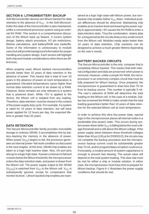
USER’S GUIDE
050396 55/173
56
SECTION 6: LITHIUM/BATTERY BACKUPSoft Microcontroller devices are lithium backed for dataretention in the absence of VCC. In the Soft Microcon-troller the state of the microcontroller is also maintained,unlike a conventional processor system using an exter-nal NV RAM. This section is a comprehensive discus-sion of the lithium back up feature. It covers systemdesign, battery attach procedure, I/O pin restrictions,lifetime calculations, and battery/RAM size tradeoffs.Some of the information is unnecessary to moduleusers but will provide background information for properhandling and system design. Each section will highlightboth chip and module considerations when there are dif-ferences.
When properly used, lithium backed microcontrollersprovide better than 10 years of data retention in theabsence of power. This means that a total of over 10years in the absence of power at room temperature isguaranteed. Elevated temperatures cause higher thannormal data retention current to be drawn by a RAM.However, these remarks are only relevant to a systemthat is powered down. While +5V is applied to thedevice, the lithium cell is isolated from any loading.Therefore, data retention must be viewed in the contextof the power supply duty cycle. For example, if a systemis rated for 10 years of data retention, but will havepower applied for 12 hours per day, the expected life-time is greater than 20 years.
DATA RETENTIONThe Secure Microcontroller family provides nonvolatilestorage in ordinary SRAM. It accomplishes this by bat-tery–backing the memory in the absence of power.When power (VCC) begins to fail, the processor gener-ates an internal power–fail reset condition as discussedin the next chapter. At this time, SRAM chip enables aretaken to a logic high inactive state. Also, I/O port pinsalso go to a logic high state. If power continues to fall andcrosses below the lithium threshold, the microprocessorenters the data retention state, and power is drawn fromthe lithium cell. The power supply output to the SRAM(VCCO) is switched from VCC to the lithium cell. VCC issubsequently ignored, except for comparators thatmonitor its level. Lithium backed chip enables are main-
tained at a logic high state with lithium power, but non–backed chip enables follow VCC down. Individual prod-uct differences should be observed. Maintaining chipenables at an inactive level and lowering the power sup-ply to approximately +3V causes the NV RAM to enter adata retention state. Thus the combination retains datafor a long period as the circuits draw a very small currentfrom the lithium cell. Modules easily attain better than10 years of data retention. Chip solutions can bedesigned to achieve a much greater lifetime dependingon the user’s needs.
BATTERY BACKED CIRCUITSThe Secure Microcontroller is the only computer that iscompletely lithium backed. This means that both inter-nal configuration and data are preserved when power isremoved. However, unlike a simple NV RAM, the micro-processor is an extremely complex circuit that must befully prepared for lithium backup. Once prepared, themicroprocessor is guaranteed to draw less than 75 nAfrom its backup source. This number is typically 5 nA.The user’s selection of RAM will determine the totalloading on the lithium cell. In the case of a module, Dal-las has screened the RAM to make certain that the totalloading guarantees better than 10 years of data reten-tion for the selected lithium cell at room temperature.
In order to achieve this ultra–low power state, speciallogic in the microprocessor places all internal nodes in apredictable (low power) state. This occurs during sys-tem power down while VCC is falling below the reset volt-age threshold and is still above the lithium voltage. If thepower supply slews between these threshold voltagesfaster than 40 µs (130 µs for DS5001/2), the circuits maynot complete the backup procedure and the micropro-cessor backup current could be substantially greaterthan 75 nA, and/or program/data corruption could occur.Fortunately, a modest amount of system capacitance isenough to prevent fast slewing. The actual value willdepend on the total system loading. This slew rate mustbe met for either a chip or module solution. In eithercase, the microprocessor must have time to prepare forlithium backup. Figure 6–1 illustrates the power supplyconditions that should be met.
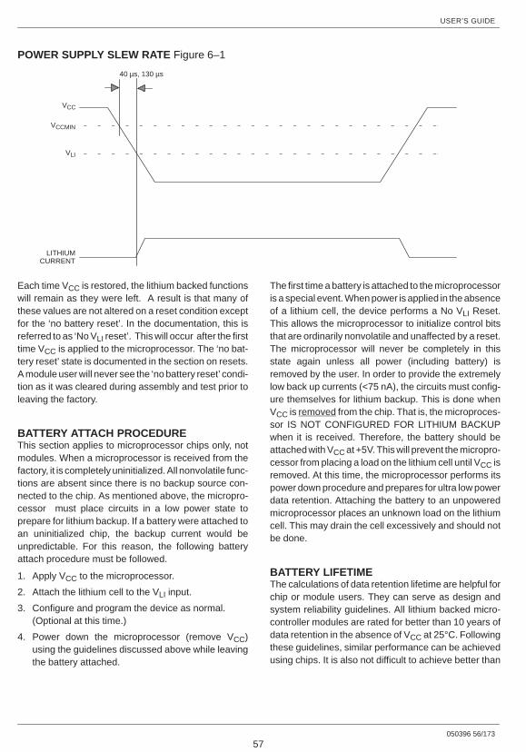
USER’S GUIDE
050396 56/173
57
POWER SUPPLY SLEW RATE Figure 6–1
40 µs, 130 µs
VCC
VCCMIN
VLI
LITHIUMCURRENT
Each time VCC is restored, the lithium backed functionswill remain as they were left. A result is that many ofthese values are not altered on a reset condition exceptfor the ‘no battery reset’. In the documentation, this isreferred to as ‘No VLI reset’. This will occur after the firsttime VCC is applied to the microprocessor. The ‘no bat-tery reset’ state is documented in the section on resets.A module user will never see the ‘no battery reset’ condi-tion as it was cleared during assembly and test prior toleaving the factory.
BATTERY ATTACH PROCEDUREThis section applies to microprocessor chips only, notmodules. When a microprocessor is received from thefactory, it is completely uninitialized. All nonvolatile func-tions are absent since there is no backup source con-nected to the chip. As mentioned above, the micropro-cessor must place circuits in a low power state toprepare for lithium backup. If a battery were attached toan uninitialized chip, the backup current would beunpredictable. For this reason, the following batteryattach procedure must be followed.
1. Apply VCC to the microprocessor.
2. Attach the lithium cell to the VLI input.
3. Configure and program the device as normal.(Optional at this time.)
4. Power down the microprocessor (remove VCC)using the guidelines discussed above while leavingthe battery attached.
The first time a battery is attached to the microprocessoris a special event. When power is applied in the absenceof a lithium cell, the device performs a No VLI Reset.This allows the microprocessor to initialize control bitsthat are ordinarily nonvolatile and unaffected by a reset.The microprocessor will never be completely in thisstate again unless all power (including battery) isremoved by the user. In order to provide the extremelylow back up currents (<75 nA), the circuits must config-ure themselves for lithium backup. This is done whenVCC is removed from the chip. That is, the microproces-sor IS NOT CONFIGURED FOR LITHIUM BACKUPwhen it is received. Therefore, the battery should beattached with VCC at +5V. This will prevent the micropro-cessor from placing a load on the lithium cell until VCC isremoved. At this time, the microprocessor performs itspower down procedure and prepares for ultra low powerdata retention. Attaching the battery to an unpoweredmicroprocessor places an unknown load on the lithiumcell. This may drain the cell excessively and should notbe done.
BATTERY LIFETIMEThe calculations of data retention lifetime are helpful forchip or module users. They can serve as design andsystem reliability guidelines. All lithium backed micro-controller modules are rated for better than 10 years ofdata retention in the absence of VCC at 25°C. Followingthese guidelines, similar performance can be achievedusing chips. It is also not difficult to achieve better than
USER’S GUIDE
050396 57/173
58
10 years depending on the user’s actual environmentand design goals.
The system lifetime can be determined from threeparameters: 1) Data retention current, 2) Lithium cellcapacity, 3) Lithium self–discharge. Current productionlithium cells have extremely good self–discharge per-formance. Manufacturer’s data and Dallas Semicon-ductor characterization has determined that the self–discharge of a coin cell lithium battery is less than 0.5%per year at 25°C. Consequently, even after 15 years ofshelf life, the lithium cell would have 90% of its capacityremaining. Therefore when using a lithium coin cell, theself–discharge mechanism is not a consideration forrating equipment life.
Data retention current is a combination of RAM, micro-processor, Real–time clock (RTC), and other lithium
backed circuits, if any. In a Dallas module, these arescreened for combination with the appropriate battery.In using a chip, the user must balance the size/cost of alarger lithium cell with the data retention current/cost ofSRAMs.
When designing a chip–based system and selecting theappropriate SRAM, the important specification is dataretention current. This is not the same as standby cur-rent. Data retention current should be specified withCE = VIH and VCC=3V. This specification is usuallyavailable at 25°C, and possibly for other temperatures.Selected RAMs have been provided in chapter 5 withthe manufacturer specified data retention current. Thelifetime calculations are illustrated below. The formulafor data retention life in years is as follows:
Battery capacity in amp hours
Data retention current in amps * # days in a year * # of hours in a day
As an example, the Microprocessor rated for 75 nA,SRAM for 500 nA, RTC for 400 nA for a total of 950 nA.
A Panasonic CR1632 lithium cell is used with a capacityof 120 mAh.
120 * 10–3 120 * 10–3
= = 14 years(75 + 500 + 400) * 10–9 * 24 * 365) 8.54 * 10–3
Thus a system with less than 1 µA of data retention cur-rent and a CR1632 lithium cell will achieve well over 10years of data retention in the absence of VCC. Referringto the recommended RAM chart in the previous section,the user will find a variety of RAMs that allow this at roomtemperature. It makes no difference if the system oper-ates at 70°C, as long as data retention is at 25°C. If stor-age is at elevated temperature, than the data retentioncurrent should be derated accordingly. If the manufac-turer does not specify data retention current over tem-perature, a conservative number is a 70% increase per10°C. Thus if a RAM in data retention mode draws 1 µAat 25°C, it will draw approximately 1.7 µA at 35°C.
A second example illustrates the case of elevated tem-perature storage.
In this example, the system is constructed using aDS5001FP chip with a Sony CXK581000P–LL 128K x 8SRAM. The system will be stored at 40°C. As shown inthe table in chapter 5, the data retention current of thisRAM is 2.4 µA at 40°C. The DS5001FP data retentioncurrent will actually drop as temperature increases, sothe maximum of 75 nA is conservative. This gives a totaldata retention current of 2475 nA. In this system, aRayovac BR2325 with a capacity of 180 mAh is used.
180 * 10–3 180 * 10–3
= = 8.3 years (2400 + 75) * 10–9 * 24 * 365) 21.68 * 10–3
Note that these ratings are for continuous data retentionso VCC is assumed absent for the entire period. Actual
performance have a longer lifetime based on the ratio oftime when VCC is applied vs. data retention time.

USER’S GUIDE
050396 58/173
59
LITHIUM BATTERY USAGEIn the vast majority of applications, lithium batteries pro-vide a reliable means of backing up data and configura-tion. The voltage varies only slightly over its useful life,so it is difficult to measure capacity. A CR chemistry willbegin life at 3.3V and drop to 2.9V near the end of life.As a consequence, some users choose to incorporatebattery clips so that lithium cells are easily replaced.This is not recommended since such clips are suscepti-ble to shock and vibration. It is possible that the connec-tion to a lithium cell would be momentarily lost duringsuch a shock, resulting in a potential loss of data. There-fore, soldered battery tabs are recommended. If a userelects to use a battery clip with a capacitor (to supportmomentary disconnect), the leakage of the capacitorshould be considered in the lifetime calculations.
FRESHNESS SEALThe Secure Microcontroller family is designed to maxi-mize the lifetime of a lithium backup source. The circuitsdescribed above contribute to a long life. There is onefurther provision that will benefit users that intend tostore their systems in an unpowered state, but that donot require it to retain data during this period. An exam-ple might be a completed system stored in inventory.Since data retention is not required, there is no benefit tousing even the modest lithium current that will normallybe drawn. For this reason, Secure Microcontrollers
incorporate the Freshness Seal. The Freshness Sealelectrically isolates the lithium cell from any externalloading. Thus even in the absence of power, the SRAMand Real–Time Clock leakage currents will not bedrawn from the lithium cell for as long as the FreshnessSeal is applied.
This feature is available to module users of the DS5000series [DS5000(T), DS2250T] and all users of theDS5001/2 series [DS5001FP, DS5002FP, DS2251T,DS2252T]. In the case of DS5000 and DS2250 mod-ules, the factory ships these with the Freshness Sealapplied. In the case of a DS5001, DS5002 seriesdevice, the Freshness Seal can be applied via the Boot-strap Loader at any time. Thus if the Freshness Seal isnot removed, the time that a Secure Microcontrollerbased system is stored in inventory will not reduce thedata retention lifetime since the lithium cell is unloaded.
To clear the Freshness Seal, simply apply VCC. On aDS5000 series device, the Freshness Seal can not berestored by the user. Therefore, if Freshness Seal isdesired for storage, the part should not be powered upwhen received or installed. Since a DS5001/DS5002series device can invoke the Freshness Seal via theLoader, this restriction does not apply. To invoke theFreshness Seal on a DS5001, DS5002 series device,the “N” command should be issued to the BootstrapLoader.
IMPORTANT APPLICATION NOTE
The pins on a Secure Microcontroller chip or module are generally as resilient as other CMOS circuits. They have nounusual susceptibility to electrostatic discharge (ESD) or other electrical transients. However, no pin on a SoftMicrocontroller chip or module should ever be taken to a voltage below ground. Negative voltages on any pincan turn on internal parasitic diodes that draw current directly from the battery. If a device pin is connected to the“outside world” where it may be handled or come in contact with electrical noise, protection should be added to pre-vent the device pin from going below –0.3V. It is also common for power supplies to give a small undershoot on powerup, which should be prevented. Application Note 93, Design Guidelines for Microcontrollers Incorporating NV RAM,discusses how to protect devices against these conditions.
USER’S GUIDE
050396 59/173
60
SECTION 7: POWER MANAGEMENTIntroductionAll Dallas Semiconductor microcontrollers are imple-mented using fully static CMOS circuitry for low powerconsumption. Power consumption is a linear function ofcrystal frequency. Two software initiated modes areavailable for further power saving at times when proces-sing is not required and VCC is at normal operating volt-age. These are the Idle and Stop modes. The additionalthird mode is the Data Retention or Zero Power Statewhich is made possible by the on–chip, circuitry. Thecontrol and status bits which apply to these operatingmodes are contained in the PCON register and are sum-marized in Figure 7–1. In addition, Table 7–1 summa-rizes the state of external pins in each of these modes.
Idle ModeThe Idle mode suspends activity of the CPU. However,the on–chip I/O function, including the timer/counters,and serial port continue their operation. This greatly re-duces the number of switching nodes and thereby dra-matically reduces the total power consumption of thedevice. The Idle mode is useful for applications in whichlower power consumption is desired with fast responseto external interrupts but no other processing.
Software can invoke the Idle mode by setting the IDL bitin the PCON register (PCON.0) to a logic 1 as shown in
Figure 7–1. The instruction which sets this bit will be thelast instruction executed before Idle mode operation be-gins. Once in the Idle mode, the microprocessor pre-serves the entire CPU status including the Stack Point-er, Program Counter, Program Status Word,Accumulator, and RAM. There are two ways to termi-nate the Idle mode. The first is from an interrupt whichhas been previously enabled prior to entering Idlemode. This will clear the IDL bit in the PCON registerand will cause the CPU to enter the interrupt service rou-tine as normal. When the RETI instruction is executed,the next instruction which will be executed is the onewhich immediately follows the instruction that set theIDL bit.
The second method of terminating the Idle mode is by aReset. At this time the IDL bit is cleared and the CPU isplaced in the reset state. Since the clock oscillator con-tinues to run in the Idle mode, an oscillator start up delay(referred to as tPOR in the AC Electrical Specifications)will not be generated following the reset. Two machinecycles are required to complete the reset operation (24oscillator periods). It should be noted that the WatchdogTimer continues to run during Idle and that a reset fromthe on–chip Watchdog Timer will terminate Idle mode.
CONTROL/STATUS BITS FOR POWER CONTROL Figure 7–1
Bit Description:
PCON.6: POR
“Power On Reset” Indicates that the previous reset was initiated during a Power On sequence.
Initialization: Cleared to a 0 when a Power On Reset occurs. Remains at 0 until it is set to a1 by software.
Read Access: Can be read normally at any time.
Write Access: Can be written only by using the Timed Access register.
PCON.5: PFW
“Power Fail Warning” Indicates that a potential power failure is in progress. Set to a 1 when VCCvoltage is below the VPFW threshold. Cleared to a 0 immediately following aread of the PCON register. Once set, it will remain set until read regardlessof VCC.
Initialization: Cleared to a 0 during a Power–On Reset.
Read Access: Can be read normally at any time.

USER’S GUIDE
050396 60/173
61
Write Access: Cannot be written.
PCON.3: EPFW
“Enable Power Fail Interrupt”: Used to enable or disable the Power Fail Interrupt. When EPFW is set to a 1,
it will be enabled; it will be disabled when EPFW is cleared to a 0.
Initialization: Cleared to a 0 on any type of reset.
Read Access: Can be read normally anytime.
Write Access: Can be written normally anytime.
PCON.1: STOP
“Stop”: Used to invoke the Stop mode. When set to a 1, program execution will ter-minate immediately and Stop mode operation will commence. Cleared to a 0when program execution resumes following a hardware reset.
Initialization: Clear to a 0 on any type of reset.
Read Access: Can be read anytime.
Write Access: Can be written only by using the Timed Access register.
PCON.0: IDL
“Idle”: Used to invoke to Idle mode. When set at a 1, program execution will behalted and will resume when the Idle bit is cleared to 0 following an interruptor a hardware reset.
Initialization: Cleared to 0 on any type of reset or interrupt.
Read Access: Can be read normally anytime.
Write Access: Can be written normally anytime.
PIN STATES IN IDLE/STOP MODES Table 7–1
MODEPROGRAMMEMORY ALE PSEN P0 P1 P2 P3
Idle Byte–wide 1 1 Port Data Port Data Port Data Port Data
Idle Expanded 1 1 Hi–Z Port Data Address Port Data
Stop Byte–wide 1 0 Port Data Port Data Port Data Port Data
Stop Expanded 1 0 Hi–Z Port Data Port Data Port Data
Stop ModeThe Stop mode is initiated by setting the STOP bit in thePCON register (PCON.1). The operation of the oscilla-tor is halted in the Stop mode so that no internal clockingsignals are produced for either the CPU or the I/O cir-cuitry. An External Reset via the RST pin is the onlymeans of exiting this mode without powering down (VCCtaken below VCCmin) and then back up to produce a
Power On Reset. The STOP bit may only be set by usingthe Timed Access software procedure described in Sec-tion 8. Since the oscillator is disabled in this mode, theWatchdog Timer will cease operation. When the exter-nal reset signal is issued to terminate the Stop mode, a21,504 clock delay will be generated to allow the clockoscillator to start up and its frequency to stabilize as isdone for a Power On Reset as described in Section 10.

USER’S GUIDE
050396 61/173
62
The original contents of those Special Function regis-ters that are initialized by a reset are lost.
Voltage Monitoring CircuitryThe on–chip voltage monitoring circuitry automaticallyplaces the microprocessor in its Data Retention state inthe absence of VCC. It insures that the proper internalcontrol signals are generated and that power from thelithium cell is applied at the proper times so that the Pro-gram/Data RAM, data in the Scratchpad Registers andcertain Special Function Registers remain unchangedwhen VCC is cycled on and off. In addition, an interrupt isavailable for signaling the processor of an impending
power fail condition so that the operational state of theprocessor can be saved just prior to entering the DataRetention.
The voltage monitoring circuitry recognizes three volt-age thresholds below nominal operating voltage. Thesethresholds are identified as VPFW (Power Fail Warningvoltage), VCCmin (minimum operating voltage), and VLI(lithium supply) voltage. These thresholds are used toinitiate required actions within the microprocessor dur-ing situations when VCC power is cycled on and off. Thetiming diagram shown in Figure 7–2 illustrates key inter-nal activities during power cycling.
SECURE MICROCONTROLLER POWER CYCLING TIMING Figure 7–2
tCSU
tPOR
tF
VPFW
VCCMIN
VLI
VCC
INTERRUPTSERVICEROUTINE
CLOCKOSC.
INTERNALRESET
LITHIUMCURRENT
USER’S GUIDE
050396 62/173
63
Power Fail InterruptWhen VCC is stable, program execution proceeds asnormal. If VCC should decay from its nominal operatingvoltage and drop to a level below the VPFW threshold,then the internal PFW status flag (PCON.5) will be set.In addition, a Power Fail Warning interrupt will be gener-ated if it has been enabled via the EPFW control bit(PCON.3). The purpose of these indicators is to warnthe processor of a potential power failure.
The VPFW threshold is above the specified minimumvalue for VCC (VCCmin) for full processor operation. TheVPFW threshold is selected so that with a reasonablepower supply slew rate, ample time is allowed for the ap-plication software to save all critical information whichwould otherwise be lost in the absence of VCC. Such in-formation may include the states of the Accumulator,Stack Pointer, Data Pointer, and other Special Functionregisters which are initialized with a reset when VCCvoltage is applied once again. Saved data can beplaced into Scratchpad RAM or Byte–wide NV RAM.Through the use of the Power Fail Warning interrupt, anorderly shutdown of the system may be performed priorto the time that processor operation is halted in theevent that VCC voltage is removed entirely.
The PFW flag is set to a logic 1 whenever the VCC levelis below the VPFW threshold. It is cleared in one of twoways: 1) a read of the PFW bit from software, or 2) aPower On Reset. If VCC is still below the VPFW thresholdwhen the bit is cleared, then the PFW bit will be immedi-ately set once again. An interrupt will be generated anytime that both the EPFW bit and the PFW flag are set.
Total Power FailureIf VCC voltage should fall below the VCCmin threshold,processor operation will halt. This is done by first placingthe CPU in a reset condition and then stopping the inter-nal clock oscillator circuit, as illustrated in Figure 7–2. Atthis time the interface to the Program/Data RAM is dis-abled by pulling the CE line high. This action guaranteesan orderly shutdown for the lithium-backed RAM.
The microprocessor is automatically placed in the DataRetention state, if VCC voltage drops below VLI, the con-trol circuitry accomplishes this by switching the internalpower supply line (VCCI) from pin to the lithium powersource. At this time, data is retained and no power isdrawn from VCC.
When power is once again applied to the system, theVCC voltage will eventually cross the VLI threshold.When this action is detected, the microprocessor willautomatically switch its internal supply line from the lithi-um source back to the VCC pin. When VCC voltageeventually goes above the VCCmin threshold, the clockoscillator is allowed to start up and an internal Power OnReset cycle is executed. Part of the cycle involves aconsiderable delay that is generated to allow the clockoscillator frequency to stabilize. Activity on the RST pinis ignored until this sequence is completed. The time re-quired for this cycle is shown as tPOR in Figure 7–2 andis specified in the AC Electrical Specifications. A de-tailed description of the Power On reset cycle operationis given in Section 10.
Typically, the time taken for the Power On Reset cyclewill be longer to complete than it takes for VCC to riseabove the VPFW threshold. In this case the internal PFWflag will be reset before execution of the user’s programbegins as illustrated in Figure 7–2. If the Power On Re-set cycle completes before VCC>VPFW, then PFW willbe set again as a result of VCC<VPFW during user soft-ware execution. A Power Fail Interrupt will occur at thistime if the EPFW bit is enabled. A user should monitorthe POR bit to know the power supply status. Refer toFigure 7–3 for details.
Partial Power FailuresTwo cases of partial power failure can occur in whichVCC voltage does not go through a completed power failcycle as described above. The first case is that in whichVCC drops below the VCCmin threshold and then returnsto its nominal level without going below the VLI thresh-old. The second case is that in which VCC drops belowthe VPFW threshold and then returns to its nominal levelwithout going below the VCCmin threshold. Both of thesecases are very possible in a system application andcould be caused by a “brownout” condition on an ACpower line.
The first case is indistinguishable by the software fromthe complete power fail cycle which was previously de-scribed. When VCC drops below VPFW the PFW flag willbe set and the clock oscillator will be stopped when VCCdrops below VCCmin. The only operational difference isthat if VCC never drops below the VLI threshold, the in-ternal power supply line will never be switched over tothe lithium cell. When VCC rises back above the VCCmin

USER’S GUIDE
050396 63/173
64
threshold, the Power On Reset cycle will be executed asbefore. As a result, no special processing is required insoftware to accommodate this case.
In the case that VCC dips without going below VLI, thePFW flag will be set and a Power Fail Warning interruptwill still occur when VCC drops below the VPFW thresh-old. The PFW flag will remain set until it is cleared by ei-ther a reset of the flag by the software or by a Power Oncycle. If it is cleared while VCC is still below the VPFWthreshold, it will be immediately set again. If it is clearedafter VCC has risen back above the VPFW threshold,
then it will remain cleared until the next time VCC goesbelow VPFW.
As long as the PFW flag is set, an interrupt condition isdefined if EPFW is set. If the software executes a ser-vice routine in response to a PFW interrupt and exits theservice routine with the PFW flag still set, then the pro-cessor will be immediately interrupted again. In a typicalapplication, however, the Power Fail Interrupt serviceroutine would test the PFW flag in a conditional loop todetermine if VCC has risen back above VPFW and wouldthen return control to the main program in response tothe event. See Figure 7–3 for details.
SECURE MICROCONTROLLER POWER MANAGEMENT Figure 7–3
POR = 0?
RUN NORMALRESET ROUTINE
SET POR
PFW = 1?
LONG POWER–UPSLEW RATE, KEEP
CHECKING
SET EPFWPOWER–FAILINTERRUPT
POWER ONBOOT ROUTINE
NO
NO
YES
YES
POWER–FAIL WARNINGINTERRUPT VECTOR
POWER HAS FALLEN BELOW VPFW,CLEAR PFW FLAG BY READING
(READ PCON)
SAVE CRITICAL DATA TO NVRAM;PREPARE FOR POWER FAILURE
POWER HASRETURNED,
RESUME
VOLTAGE IS STILL BELOWVPFW, NOT SAFE TO RUN
NO
YESOPERATION
PFW = 1?
RESET VECTOR
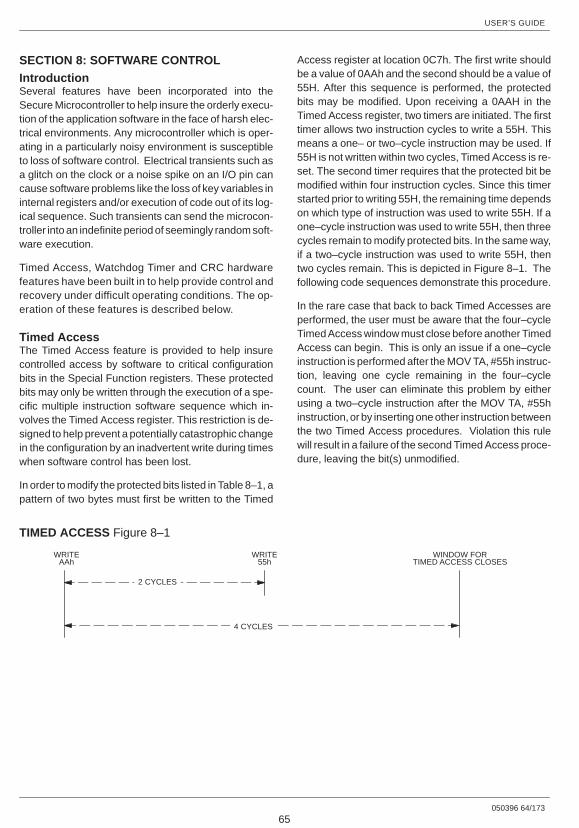
USER’S GUIDE
050396 64/173
65
SECTION 8: SOFTWARE CONTROLIntroductionSeveral features have been incorporated into theSecure Microcontroller to help insure the orderly execu-tion of the application software in the face of harsh elec-trical environments. Any microcontroller which is oper-ating in a particularly noisy environment is susceptibleto loss of software control. Electrical transients such asa glitch on the clock or a noise spike on an I/O pin cancause software problems like the loss of key variables ininternal registers and/or execution of code out of its log-ical sequence. Such transients can send the microcon-troller into an indefinite period of seemingly random soft-ware execution.
Timed Access, Watchdog Timer and CRC hardwarefeatures have been built in to help provide control andrecovery under difficult operating conditions. The op-eration of these features is described below.
Timed AccessThe Timed Access feature is provided to help insurecontrolled access by software to critical configurationbits in the Special Function registers. These protectedbits may only be written through the execution of a spe-cific multiple instruction software sequence which in-volves the Timed Access register. This restriction is de-signed to help prevent a potentially catastrophic changein the configuration by an inadvertent write during timeswhen software control has been lost.
In order to modify the protected bits listed in Table 8–1, apattern of two bytes must first be written to the Timed
Access register at location 0C7h. The first write shouldbe a value of 0AAh and the second should be a value of55H. After this sequence is performed, the protectedbits may be modified. Upon receiving a 0AAH in theTimed Access register, two timers are initiated. The firsttimer allows two instruction cycles to write a 55H. Thismeans a one– or two–cycle instruction may be used. If55H is not written within two cycles, Timed Access is re-set. The second timer requires that the protected bit bemodified within four instruction cycles. Since this timerstarted prior to writing 55H, the remaining time dependson which type of instruction was used to write 55H. If aone–cycle instruction was used to write 55H, then threecycles remain to modify protected bits. In the same way,if a two–cycle instruction was used to write 55H, thentwo cycles remain. This is depicted in Figure 8–1. Thefollowing code sequences demonstrate this procedure.
In the rare case that back to back Timed Accesses areperformed, the user must be aware that the four–cycleTimed Access window must close before another TimedAccess can begin. This is only an issue if a one–cycleinstruction is performed after the MOV TA, #55h instruc-tion, leaving one cycle remaining in the four–cyclecount. The user can eliminate this problem by eitherusing a two–cycle instruction after the MOV TA, #55hinstruction, or by inserting one other instruction betweenthe two Timed Access procedures. Violation this rulewill result in a failure of the second Timed Access proce-dure, leaving the bit(s) unmodified.
TIMED ACCESS Figure 8–1
2 CYCLES
4 CYCLES
WRITEAAh
WRITE55h
WINDOW FORTIMED ACCESS CLOSES
USER’S GUIDE
050396 65/173
66
This code allows the reset of the Watchdog Timer:
MOV 0C7H,#0AAH ; 1st TA ValueMOV 0C7H,#055H ; 2nd TA Value 2 CyclesSETB IP.7 ; Reset Watchdog Timer 1 Cycle
The Watchdog Timer bit may have been set using ORL IP, #80H whichtakes two cycles.
This code allows the reset of the Watchdog Timer using a different ap-proach:
MOV A, #55H ; Setup Acc for fast writeMOV 0C7H, #0AAH ; 1st TA ValueMOV 0C7H, A ; 2nd TA Value 1 CycleMOV A, IP ; Get Current IP 1 CycleORL A, #80H ; Prepare for fast write 1 CycleMOV IP, A ; Reset Watchdog Timer 1 Cycle
Note that a new value for IP could have been retrieved from any directregister instead of the current IP.
The bits which are write access–protected by the Timed Access function are listed in Table 8–1.
TIMED ACCESS PROTECTED CONTROL BITS Table 8–1
BIT NAME MICRO VERSION LOCATION DESCRIPTION
EWT All Secure Micro PCON.2 Enables the Watchdog Timer Reset function
RWT All Secure Micro IP.7 Resets the Watchdog Timer count
STOP All Secure Micro PCON.1 Stop Mode Enable
POR All Secure Micro PCON.6 Power On Reset
PAA DS5000 series MCON.1 Partition Address Access bit (protects PA3–0)
PA3–0 DS5001, DS5002series
MCON.7–4 Partition Address bits
AE DS5001, DS5002series
RPCTL.4 Access Enable
The Secure Microcontroller family has a variety of con-trol bits that are critical to the correct operation of theprocessor. Several of these are nonvolatile and will notbe altered by a reset. Thus they must be protected froman accidental write by software that has gone out of con-trol. This is a possibility in all microprocessor based sys-tems, especially those in an industrial environment.While the Watchdog Timer will recover from this condi-tion, the critical bits must be protected during the intervalbefore the time–out of the Watchdog Timer.
The Secure Microcontroller family actually has two lev-els of protection for these critical bits. The most criticalSFR bits can only be altered using the Bootstrap Load-er. An example is the Range function that determinesthe total memory. There is no need for an application tomodify this bit during normal operation. For those criticalbits that might need to be modified during normal opera-tion, the Timed Access procedure protects against aninadvertent write operation.

USER’S GUIDE
050396 66/173
67
Timed Access provides a statistical protection. It isunlikely that randomly generated states will correctlymatch the sequence and timing required to bypass theTimed Access logic. Presented below is a brief justifica-tion for each bit that is protected by Timed Access.
The EWT bit is protected to prevent errant software fromdisabling the Watchdog Timer. The Watchdog is one ofthe important mechanisms that assure correct opera-tion and should not be turned off accidentally. RWT isthe bit that software uses to restart the Watchdog time–out. The Secure Microcontroller makes this more diffi-cult by Timed Access protecting the bit. Thus softwaremust “really” intend to reset the time–out in order to doso. Note that the Watchdog Timer is disabled in Stopmode. Critical applications which rely on the WatchdogTimer should exercise caution if the application will uti-lize Stop mode.
POR informs the software of the power supply condi-tion. Specifically, it means the power has previouslydropped below the VCCMIN level and returned to nor-mal. In many systems, this is a unique condition thatrequires interaction with external hardware. Protectingthis bit with a Timed Access procedure prevents themicro from accidentally performing a power on resetprocedure.
On a DS5000 series device, the PAA bit allows softwareto alter the Partition. If this is done accidentally, theresulting configuration could be unrecoverable withouthuman intervention. This could mean selecting a Parti-tion that is outside of the user’s plan and that causes thesystem to fail. In a like manner, the PA3–0 bits on aDS5001 series device are protected through TimedAccess. As the DS5001 does not have a PAA bit, thePartition control bits are directly protected. The motiva-tion for protecting the AE bit is similar. This bit invokes aPartitionable configuration where one had not beenselected during Bootstrap loading. While there are sev-eral valid reasons to select AE, accidentally selectingthis condition might be unrecoverable without manualintervention.
Note that the Timed Access logic protects against thepossibility of a single inadvertent write modifying a criti-cal control bit. It does not protect against inadvertentlyentering a section of code that contains the correctsequence to modify a protected bit. However, the statis-tical protection does greatly improve the system’s resil-ience to a crash.
Watchdog TimerThe on–chip Watchdog Timer provides a method of re-storing proper operation during transients that causethe loss of controlled execution of software. When theWatchdog Timer is enabled, it will eventually reach atimeout condition after 122,800 machine cycles unless itis reset by the application software. An internal reset tothe CPU will be generated if the timeout condition is everreached. Software which utilizes the Watchdog Timermust periodically reset the RWT bit so that it will neverbe reached during normal operation. The reset opera-tion(s) should be inserted at critical check points in theprogram. The Watchdog Timer will monitor programexecution to insure that these check points are reached,indicating proper operation. If controlled execution ofthe software is lost so that these check points are not en-countered within the timeout period, then the WatchdogTimer will provide an automatic reset. A block diagramof the Watchdog Timer is shown in Figure 8–2.
The Special Function Register bits that are used to con-trol the Watchdog include the Enable Watchdog Timerbit (EWT; PCON.2), the Reset Watchdog Timer bit(RWT; IP.7), and the Watchdog Timer Reset status flag(WTR; PCON.4). The Watchdog Timer incorporates afree–running counter that starts counting as soon as theclock oscillator begins operation following a Power OnReset. If a 12 MHz crystal is used as the time base ele-ment, this gives a timeout period of 122.88 ms. TheWatchdog Timer Reset function is enabled with a TimedAccess write operation which sets the EWT bit to a 1. AWatchdog Timer Reset will then occur the next time thatthe free–running counter reaches its timeout condition.
Regardless of whether the Watchdog Timer will beused, it should be initialized after each reset. If theWatchdog Timer is desired, then the first step is to resetthe timer count. This is necessary since the timer is freerunning and may be about to time–out. Set the RWT bitto a logic 1 using a Timed Access procedure. This willrestart the timer with the full interval. Then enable theWatchdog Timer reset function by setting the EWT bit toa logic 1, again with a Timed Access procedure. Notethat the EWT bit only controls whether the reset isissued, not whether the timer runs. The Watchdog Timermust now be reset prior to 122,800 machine cycles or itwill reset the CPU. If the Watchdog Timer is not used,then clear the EWT bit to a logic 0 using a Timed Accessprocedure. Since the EWT bit is nonvolatile, this makescertain that the Watchdog reset function remains dis-abled.
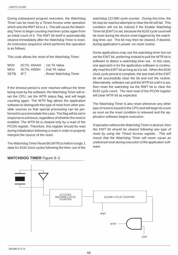
USER’S GUIDE
050396 67/173
68
During subsequent program execution, the WatchdogTimer can be reset by a Timed Access write operationwhich sets the RWT bit to a 1. This will cause the Watch-dog Timer to begin counting machine cycles again froman initial count of 0. The RWT bit itself is automaticallycleared immediately after the Watchdog Timer is reset.An instruction sequence which performs this operationis as follows.
This code allows the reset of the Watchdog Timer:
MOV 0C7H, #0AAH ; 1st TA ValueMOV 0C7H, #055H ; 2nd TA ValueSETB IP.7 ; Reset Watchdog Timer
If the timeout period is ever reached without the timerbeing reset by the software, the Watchdog Timer will re-set the CPU, set the WTR status flag, and will begincounting again. The WTR flag allows the applicationsoftware to distinguish this type of reset from other pos-sible sources so that special processing can be per-formed to accommodate this case. This flag will be set inresponse to a timeout, regardless of whether the reset isenabled. The WTR bit is cleared only by a read of thePCON register. Therefore, this register should be readduring initialization following a reset in order to properlyinterpret the source of the reset.
The Watchdog Timer Reset Bit (WTR) is held in a logic 1state for 8192 clock cycles following the time–out of the
watchdog 122,880 cycle counter. During this time, thebit may be read but attempts to clear the bit will fail. Thiscondition will not be noticed if the Enable WatchdogTimer bit (EWT) is set, because the 8192 cycle count willbe reset during the device reset triggered by the watch-dog time–out. The bit may then be cleared, if desired,during application’s power–on reset routine.
Some applications may use the watchdog timer but notset the EWT bit, preferring instead to poll the WTR bit insoftware to detect a watchdog time–out. In this case,one approach is for the application software to continu-ally read the EWT bit as long as it is set. When the 8192clock cycle period is complete, the last read of the EWTbit will successfully clear the bit and exit the routine.Alternatively, software can poll the WTR bit until it is set,then reset the watchdog via the RWT bit to clear the8192 cycle count. The next read of the PCON registerwill clear WTR bit as expected.
The Watchdog Timer is also reset whenever any othertype of reset is issued to the CPU and will begin its countas soon as the reset condition is released and the ap-plication software begins execution.
If operation without the Watchdog Timer is desired, thenthe EWT bit should be cleared following any type ofreset by using the Timed Access register. This willinsure that the Watchdog Timer will never cause anundesired reset during execution of the application soft-ware.
WATCHDOG TIMER Figure 8–2
12 CLOCKMACHINE CYCLE
COUNTER122,800 CYCLE COUNTER
RWT
WTR
EWT
USER’S GUIDE
050396 68/173
69
WATCHDOG TIMER CONTROL BITS
Bit Description:
PCON.4: WTR
“Watchdog Timer Reset” Set to a 1 when a Watchdog Timer timeout occurs. If Watchdog Timer Resetis enabled, this will indicate the cause of the reset. Cleared to 0 immediatelyfollowing a read of the PCON register.
Initialization: Set to a 1 after a Watchdog Timeout. Cleared to a 0 on a No–VLI Power OnReset. Remains unchanged during other types of resets.
Read Access: May be read normally anytime.
Write Access: Cannot be written.
PCON.2: EWT
“Enable Watchdog Timer Used to enable or disable the Watchdog Timeout Reset. The Reset isReset”: enabled if EWT is set to a 1 and will be disabled if EWT is cleared to a 0. This
bit affects the generation of a reset condition, not the running of the Watch-dog Timer.
Initialization: Cleared to a 0 on a No–VLI Power On Reset. Remains unchanged duringother types of resets.
Read Access: May be read normally anytime.
Write Access: Can be written only by using the Timed Access register.
IP.7: RWT
“Reset Watchdog Timer”: When set to a 1, the Watchdog Timer count will be reset, and counting willbegin again. The RWT bit will then automatically be cleared again to 0. Writ-ing a 0 into this bit has no effect. This bit should be set prior to EWT, as thetimers are free–running.
Initialization: Cleared to a 0 on any reset.
Read Access: Cannot be read.
Write Access: Can be written only by using the Timed Access register.
CRC MEMORY VERIFICATIONWhen using nonvolatile memory, there is always thepotential for a catastrophic event to alter the memorycontents. These events include lightning, massive ESD,severe mistreatment, etc. No nonvolatile technology isimmune to these events. To compensate, the DS5001series contains a CRC function that allows for automaticverification of memory on power up. The CRC functionis also available to the user for application software use.Note that this is not available on DS5000 series devices[DS5000(T), DS2250T, DS5000FP].
If the CRC option is selected through the BootstrapLoader, then on power up or after a Watchdog Timer
reset, the microcontroller will automatically perform aCRC–16 on the memory. The range over which it is per-formed is selected by the user, and the result iscompared to a pre–stored value. If the CRC–16 is inerror, the DS5001 series microcontroller will enter theBootstrap Loader and wait. From the perspective of thesystem, the appears held in a reset condition.
To support this function, the CRC register shown belowis accessible through the Bootstrap Loader. Setting theCRC bit (LSB) enables the power–up CRC function.The loader command “W” is used to write to this register.The upper nibble of the CRC register (a hex valuebetween 0 and F) defines the address space in 4K
USER’S GUIDE
050396 69/173
70
blocks over which the CRC calculation is performed.For example, if the nibble is set to 0001b, the CRC rangeis from 0000 to 0FFFh. Once the LSB of the CRC regis-ter is set, the loader “I” command will cause the CRC ofthe specified block to be computed. The result is auto-matically stored in the last two bytes of the specifiedblock. These bytes should not be used by the applica-tion. This computation will be correct provided that theCRC range is less than or equal to the partition if PM=0.If PM=1, using 32K RAMs, the CRC range must be lessthan or equal to the program range.
If CRC is enabled, the DS5001FP will automaticallyinvoke the Bootstrap Loader on either power–up or a
Watchdog timeout and the CRC check will be per-formed. If an error is detected, the Bootstrap Loader willwait for reloading. If there is no error, the application willbegin at address 0000h following a reset. Automaticchecking of the CRC can be disabled by writing a 0 tothe CRC register LSB. As mentioned above, this isdone using the “W” command in loader mode. The CRChardware uses registers 0C3h and 0C2h for most andleast significant byte intermediate storage. TheDS5002FP and DS2252T do not perform a CRC checkto ensure software security.
DS5001 CRC REGISTER (Address 0C1h)
RNGE3 RNGE2 RNGE1 RNGE0 ––– ––– MDM CRC
CRC.7–4: RANGE 3–0Determines the range over which a power–up CRC will be performed.Addresses are specified on 4K boundaries.
Initialization: Reset to 0 on a No VLI reset.
Read Access: Can be read at any time.
Write Access: Cannot be written by application software. Can be written via the BootstrapLoader.
CRC.1: MDMWhen set to 1, the Bootstrap Loader will attempt to use a modem (UART)on PE4 if CRC is incorrect. This feature is no longer useful following theobsoletion of the corresponding modem devices.
Initialization: Reset to 0 on a No VLI reset.
Read Access: Can be read at any time.
Write Access: Cannot be written by application software. Can be written via the BootstrapLoader.
CRC.0: CRCWhen set to 1, a CRC check will be performed on power–up or watchdogtimeout. CRC will be checked against stored values. An error will initiateProgram Load mode. This bit will not be present in the DS5002 as the devicedoes not support the power–on CRC function.
Initialization: Reset to 0 on a No VLI reset.
Read Access: Can be read at any time.
Write Access: Cannot be written by application software. Can be written via the BootstrapLoader.
USER’S GUIDE
050396 70/173
71
CRC CODE EXAMPLE Figure 8–3
This routine tests the CRC–16 circuit in the DS5001FP
crcmsb equ 0C3hcrclsb equ 0C2h
org 00h ;after reset, CRC regs = 0000
begin:
mov p2,crcmsb ;p2=00 read crcmsb registermov p3,crclsb ;p3=00 read crclsb registermov crclsb, #075h ;check crc register operation
;data in = 75 result = E7C1mov crclsb, #08Ah ;data in = 8A result = 37A7mov crclsb, #00Bh ;data in = 0B result = 7D37mov crclsb, #075h ;data in = 75 result = 31FDmov crclsb, #0C7h ;data in = C7 result = 13B1mov crclsb, #0AAh ;data in = AA result = 0B53mov crclsb, #075h ;data in = 75 result = DA8Amov crclsb, #0C7h ;data in = C7 result = 351Amov crclsb, #055h ;data in = 55 result = F474mov crclsb, #043h ;data in = 43 result = D6B5
nop ;delay after last write and before first read;let CRC finish
mov p0 ,crcmsb ;p0=D6 read CRCMSB registermov p1 ,crclsb ;p1=B5 read CRCLSB registermov crclsb ,crclsb ;clear CRC, data in = B5 result = 00D6nop ;need delaymov crclsb ,crclsb ;cleared, data in = D6 result = 0000
nopmov p2 ,crcmsb ;p1=00 read crcmsb registermov p3 ,crclsb ;p1=00 read crclsb register
end_loop:
sjmp $end
As mentioned, the CRC–16 function is optionally avail-able to the application software. This is availableregardless of whether the automatic power–on CRC isused. Although a CRC could be computed completely insoftware, it would take much longer than using theDS5001 facility. Using the CRC–16 hardware, theDS5001 series can perform a CRC–16 on 64K bytes ofmemory in approximately 500 ms. The CRC–16 logicresides behind the two SFRs mentioned above. Thesedisplay the current CRC result and also serve as theinput locations. The software must sequentially write thememory values into the CRC LSB at location 0C2h.
After a delay of one instruction cycle, the 16–bit resultwill be available at 0C3h and 0C2h. The CRC–16 is asuperior method of checking the file validity comparedto a checksum. Using the DS5001 hardware, it can becomputed quickly. When using the CRC–16 hardwareas part of an application, the existing CRC should firstbe cleared. This is done by writing the CRC back onitself. This process makes the CRC–16 result equal to0000h. The LSB is written back twice with a delay inbetween for computation. The code example shown inFigure 8–3 displays the CRC–16 result on ports 0 and 1.

USER’S GUIDE
050396 71/173
72
SECTION 9: FIRMWARE SECURITYOne of the most unique features of the Secure Micro-controller is its firmware security. The family far sur-passes the standard offering of ROM based microcon-trollers in keeping system attackers or competitors fromviewing the contents of memory. In a standard EPROMbased microcontroller, a knowledgeable attacker candisable the EPROM security bit and have access to theentire memory contents. The Secure Microcontroller’simproved security makes it a natural choice for systemswith high security requirements such as financial trans-action terminals. However, the firmware security canalso be employed to keep competitors from copying pro-prietary algorithms. Allowing access to these algo-rithms can create an instant competitor. This sectiondescribes the security features and their application.
Also included are guidelines to using microcontrollersecurity within the framework of total system security.
As with memory map control, there are variationsbetween the different Secure Microcontroller versions.The original DS5000 has a high level of firmware secu-rity and the DS5002 has added several distinct improve-ments. Note that the DS5001 has only minimal securityand should only be applied when other physical securityis used or when security is not needed. The table belowprovides a brief summary of the versions and their secu-rity features. A detailed description of each feature fol-lows. In the description, elements that are unique to aparticular Secure Microcontroller version have that ver-sion underlined.
FEATURE DS5001 DS5000 DS5002
Security Lock Yes Yes Yes
RAM memory Yes Yes Yes
Encrypted memory None Yes, user must enable Yes
Encryption Key None 48 bits 64 bits
Encryption Key Selection None User selected True random number
Encryption Keys loaded N/A When user selects Automatic, any new load, dump
Dummy bus access None Yes, when encrypted Yes
On–chip Vector RAM None Yes, when encrypted Yes
Self–Destruct Input None None Yes
Die Top Coating None None Optional (DS5002FPM)
Random Number Generator Yes None Yes
SECURITY OVERVIEWSecurity features are useful if an application dispensesservices on a pay per service basis. Electronicallybypassing the security would allow the dispensing of theservice for free, resulting in lost revenue to the systemowner. Another common application is the transmissionof secret information. The user’s algorithm and key datacould be observed in a unsecured system, resulting in abreak in the secure transmission. The Secure Micro-controller Family is designed to protect the contents ofmemory from being viewed. This is done with a com-
bination of circuit techniques and physical security. Thecombination is a formidable defense. Regardless of theapplication, the secure microcontroller protects the con-tents of memory from tampering and observation. Thispreserves secret information, access to services, criti-cal algorithms etc. The security features of the SecureMicrocontroller include physical security against probe,memory security through cryptographic scrambling,and memory bus security preventing analysis of theCPU’s operation. The features mentioned above anddescribed below protect the application code and data.
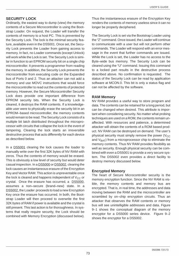
USER’S GUIDE
050396 72/173
73
SECURITY LOCKOrdinarily, the easiest way to dump (view) the memorycontents of a Secure Microcontroller is using the Boot-strap Loader. On request, the Loader will transfer thecontents of memory to a host PC. This is prevented bythe Security Lock. The lock is the minimal security fea-ture, available even in the DS5001. Once set, the Secu-rity Lock prevents the Loader from gaining access tomemory. In fact, no Loader commands (except Unlock)will work while the Lock is set. The Security Lock is simi-lar in function to an EPROM security bit on a single chipmicrocontroller. It prevents a programmer from readingthe memory. In addition, the Security Lock prevents themicrocontroller from executing code on the Expandedbus of Ports 0 and 2. Thus an attacker can not add amemory and use MOVC instructions that would forcethe microcontroller to read out the contents of protectedmemory. However, the Secure Microcontroller SecurityLock does provide one important difference fromEPROM security bits. When the Security Lock iscleared, it destroys the RAM contents. If a knowledge-able user were to physically erase the security bit in anEPROM–based microcontroller, the memory contentswould remain to be read. The Security Lock consists of amultiple bit latch distributed throughout the micropro-cessor with circuits that collapse the lock in the event oftampering. Clearing the lock starts an irreversibledestructive process that acts differently for each deviceas described below.
In a DS5001 clearing the lock causes the loader tomanually write over the first 32K bytes of NV RAM withzeros. Thus the contents of memory would be erased.This is obviously a low level of security but would detercasual inspection. In a DS5000 or DS5002, clearing thelock causes an instantaneous erasure of the EncryptionKey and Vector RAM. This action is unpreventable oncethe lock is cleared and happens independent of VCC orcrystal. Once the erasure has occurred, a DS5000,assumes a non–secure (brand–new) state. In aDS5002, the Loader proceeds to load a new EncryptionKey once the erasure has occurred. In both, the Boot-strap Loader will then proceed to overwrite the first32K bytes of RAM if power is available and the crystal isstill present. This last action is for thoroughness. In sys-tems that really require security, the Lock should becombined with Memory Encryption (discussed below).
Thus the instantaneous erasure of the Encryption Keyrenders the contents of memory useless since it can nolonger be properly deciphered.
The Security Lock is set via the Bootstrap Loader usingthe “Z” command. Once issued, the Loader will continueto communicate with a user but will not perform othercommands. The Loader will respond with an error mes-sage in the event that further commands are issued.While the Lock is set, the Loader has no access to theByte–wide bus memory. The Security Lock can becleared using the “U” command. Issuing this commandto a locked part results in the destructive processdescribed above. No confirmation is requested. Thestatus of the Security Lock can be read by applicationsoftware at MCON.0. This bit is only a status flag andcan not be affected by the software.
RAM MemoryNV RAM provides a useful way to store program anddata. The contents can be retained for a long period, butcan be changed when desired. This attribute is impor-tant when considering security. No matter what probingtechniques are used on a ROM, the contents remain un-affected. With resources and patience, a determinedattacker will obtain the contents of a ROM based prod-uct. NV RAM can be destroyed on demand. The user’sphysical security must simply remove the power (VCCand VBAT) from a microprocessor chip to eliminate thememory contents. Thus NV RAM provides flexibility aswell as security. Enough physical security can be com-bined with even a DS5001 to provide a very secure sys-tem. The DS5002 even provides a direct facility todestroy memory discussed below.
Encrypted MemoryThe heart of Secure Microcontroller security is thememory encryption function. Since the NV RAM is vis-ible, the memory contents and memory bus areencrypted. That is, in real time, the addresses and datamoving between the RAM and the microcontroller arescrambled by on–chip encryption circuits. Thus anattacker that observes the RAM contents or memorybus will see unintelligible addresses and data. Figure9–1 shows the conceptual diagram of the memoryencryptor for a DS5000 series device. Figure 9–2shows the encryptor for a DS5002.
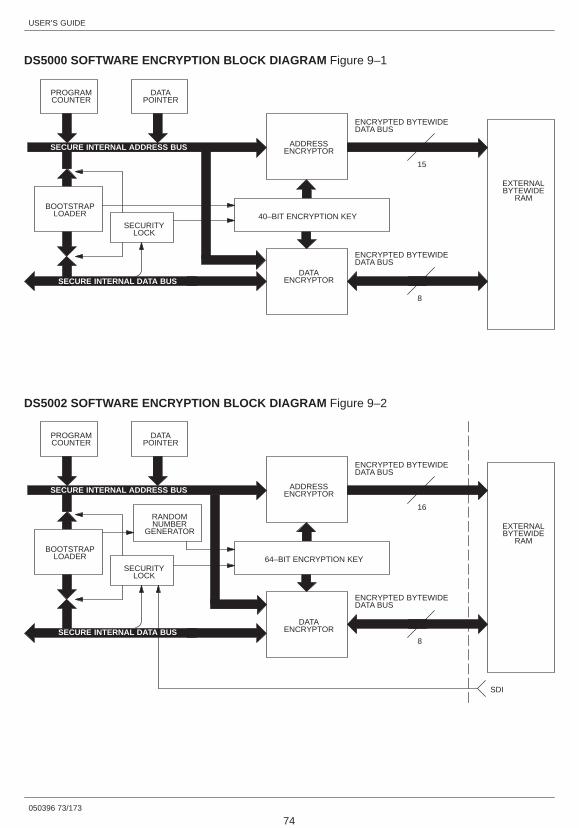
USER’S GUIDE
050396 73/173
74
DS5000 SOFTWARE ENCRYPTION BLOCK DIAGRAM Figure 9–1
PROGRAMCOUNTER
DATAPOINTER
ADDRESSENCRYPTOR
EXTERNALBYTEWIDE
RAM
40–BIT ENCRYPTION KEY
DATAENCRYPTOR
SECURITYLOCK
BOOTSTRAPLOADER
SECURE INTERNAL DATA BUS
SECURE INTERNAL ADDRESS BUS
ENCRYPTED BYTEWIDEDATA BUS
8
ENCRYPTED BYTEWIDEDATA BUS
15
DS5002 SOFTWARE ENCRYPTION BLOCK DIAGRAM Figure 9–2
PROGRAMCOUNTER
DATAPOINTER
ADDRESSENCRYPTOR
EXTERNALBYTEWIDE
RAM
64–BIT ENCRYPTION KEY
DATAENCRYPTOR
SECURITYLOCK
BOOTSTRAPLOADER
SECURE INTERNAL DATA BUS
SECURE INTERNAL ADDRESS BUS
ENCRYPTED BYTEWIDEDATA BUS
8
ENCRYPTED BYTEWIDEDATA BUS
16RANDOMNUMBER
GENERATOR
SDI
USER’S GUIDE
050396 74/173
75
In a DS5000, the encryption feature is optional. ADS5000 can be locked irrespective of its encryption andencrypted irrespective of the lock. Neither makes muchsense by itself. The encryption process is enabled byloading an Encryption Key for the first time. Prior to load-ing a Key, the DS5000 remains in a non–encryptedstate. Once encrypted, the memory interface will remainso until a part is locked, then unlocked. The process ofclearing the Security Lock deactivates the encryptioncircuits. Note that an Encryption Key of zero is still avalid Key. A DS5002 has encryption enabled at alltimes. No extra steps are required to invoke it. As dis-cussed below, the DS5002 generates its own securityKeys.
Encryption logic consists of an address encryptor and adata encryptor using separate but related algorithms.These encryptors are high speed circuits that are trans-parent to the application software. They are bidirec-tional and repeatable. That is, addresses and data thatare scrambled prior to writing to RAM will be correctlyunscrambled when reading in reverse. Each encryptoroperates with its own algorithm but both are dependenton the Encryption Key. Encryptors operate while pro-grams are being loaded so that the memory contentsare stored in its scrambled form. When programmemory is fetched, the process is reversed. Thus theactual program or data is only present in its “true” formwhile inside the microcontroller.
The address encryptor translates each “logical”address, i.e., the normal sequence of addresses thatare generated in the logical flow of a program, into anencrypted address (or physical address) at which thebyte is actually stored in RAM. Each time a logicaladdress is generated either during program loading orduring execution, the address encryptor circuits use theEncryption Key value and the address itself to form thephysical address that will be presented to the RAM onthe Byte–wide bus. The encryption algorithm is suchthat there is one and only one physical address forevery possible logical address. The address encryptoroperates over the entire memory range.
The Data Encryptor operates in a similar manner to theaddress encryptor. As each byte including opcode,operand, or data is received during Bootstrap Loading,its value is scrambled prior to storing it in RAM. Thevalue that is actually written in RAM is an encrypted rep-resentation. All values that are subsequently stored inRAM during execution also are encrypted. As each byteis read back to the CPU during execution, the internalData Encryptor restores it to its original value. Thisencryptor uses the Encryption Key and the data valueitself, but also the logical address. Thus the same datawith the same Key will have different physical values atdifferent address locations. The data encryption algo-rithm is repeatable and reversible so that with the samekey, data and address, the same encrypted value will beobtained. Note however that there are many possibleencrypted data values for each possible true value dueto the algorithms dependency on Key and address.
Using the combination of address and data encryption,the normal flow of program code is unintelligible in theNV RAM. What had been a sequential flow of addressesis now apparently random. The values stored in eachmemory location appear to have no relation to the origi-nal data. Another factor that makes analysis more diffi-cult is that all 256 possible values in each memory arevalid possibilities. Thus an encrypted value is not onlyscrambled, but it becomes another potentially validbyte.
Different memory areas are encrypted in the DS5000and DS5002. For a DS5000, all memory accessedunder CE1 can be encrypted. CE2 is not encrypted. Thisallows access to peripherals such as a Real–time Clockto be performed using CE2.
For the DS5002, encryption is performed on all bytesstored under CE1 through CE4. The memory or periph-erals accessed by PE1 through PE4 on a DS5002 arenot encrypted.
USER’S GUIDE
050396 75/173
76
Encryption AlgorithmThe Secure Microcontroller family uses a proprietaryalgorithm to encrypt memory. The DS5000FP andDS5002FP use different encryption algorithms. Theyare the result of improvements made over time in theproprietary encryptor circuits. The original DS5000FP(circa 1988) has the first version of encryptor. This wassoon improved with a second version encryptor in 1989,and remains in production today. A substantial improve-ment was made in the DS5002FP, which uses a widerKey and a more non–linear algorithm. The DS5002FPmemory encryptor uses elements of the DES (DataEncryption Standard) although not the entire algorithm.Full DES is impractical as memory encryption must beperformed in real–time on a one–to–one substitutionand not a block cypher basis. The encryption algorithmis supported by the fact that both address and data areencrypted, the algorithm and key are both secret, themost critical data can be stored on chip in vector RAM(discussed below), and the bus activity is scrambledusing dummy access (discussed below). For this rea-son, a security analysis of the DS5002FP is not simply amathematical treatment of the encryption algorithm.
Encryption KeyThe DS5000FP uses a 40–bit Encryption Key that isstored on–chip. As mentioned above, the Key is thebasis of the encryption algorithm. The resulting physicaladdresses and data are dependent on this value. Tam-pering with or unlocking the microcontroller will causethe Key to be instantaneously destroyed. If the memorycontents are encrypted, they become useless withoutthis Key. A user selects the 40–bit Key and loads it viathe Bootstrap Loader. Selecting this Key enables theencryption feature. The DS5002FP uses a 64–bit Key. Itis similarly stored on–chip in tamper resistant circuits. Inmuch the same way, this Key is the basis for the physicalvalues that are presented on the bus. Using a wider Keygives the encryption more complexity and more per-mutations that must be analyzed by an attacker. Apartfrom the width of the Key and complexity of the encryp-tor, the principal differences between the DS5000FPand DS5002FP are discussed below under Key Selec-tion and Loading.
Encryption Key Selection and LoadingOne of the significant differences between DS5000FPand DS5002FP lies in Encryption Key Management. Inthe case of a DS5000FP, the user must select a 40–bit
Key during program loading. This Key must be selectedprior to loading the microcontroller, as the memory willbe encrypted as it is loaded. The Key selection processmust be protected since an attacker that learns the Keycan reproduce the user’s code. This would be done byloading the correct Key in an unlocked DS5000FP,attaching the encrypted memory chip, and dumping thecode using the Bootstrap Loader.
The DS5002FP provides an improved Key manage-ment system. The microcontroller chooses its own64–bit Encryption Key from a number that is internallygenerated and secret. The Keys come from a true hard-ware random number generator. It is based on fre-quency differences between two on–chip ring oscilla-tors and the user’s crystal. At any time, it is unlikely thatany two DS5002FPs have the same key with 264 (1.84 *1019) combinations. There is no method to discover theKey value. No attacker can force the DS5002 to a partic-ular Key. In addition, no one can “forget” to enable theencryptor, since it is always enabled. An additionaladvantage of the secret Key is that an attacker can not“characterize” the encryptor by repeatedly loadingknown Keys and observing the result.
As mentioned above, encryption is always enabled onthe DS5002FP. Each time the Bootstrap Loader isinvoked, a new random number is prepared. If a Fill,Load, Dump, Verify, or CRC command is requested, theLoader selects the random number as a new EncryptionKey prior to accessing the memory. Execution of a Loador Fill command will result in a the data being loaded inan encrypted form determined by the value of the new-ly–generated Key. Any subsequent Dump, Verify, orCRC within the same Bootstrap session will cause thecontents of the encrypted RAM to be read out and prop-erly decrypted by the micro. Once a new Key is loaded, itwill allow all commands to work properly within the sameBootstrap session since memory access is done usingthe correct Key. Exiting and re–entering the BootstrapLoader, then doing a Dump will not work since thisaction would first result in Loading a new EncryptionKey. The microcontroller would no longer be able todecrypt the RAM contents. This extra precaution is usedregardless of the Security Lock. It prevents an attackerfrom retrieving memory through the Bootstrap Loadereven if the programmer forgets to lock the DS5002FP.Once the Security Lock is set, all Bootstrap Loaderaccess to the memory is prohibited.
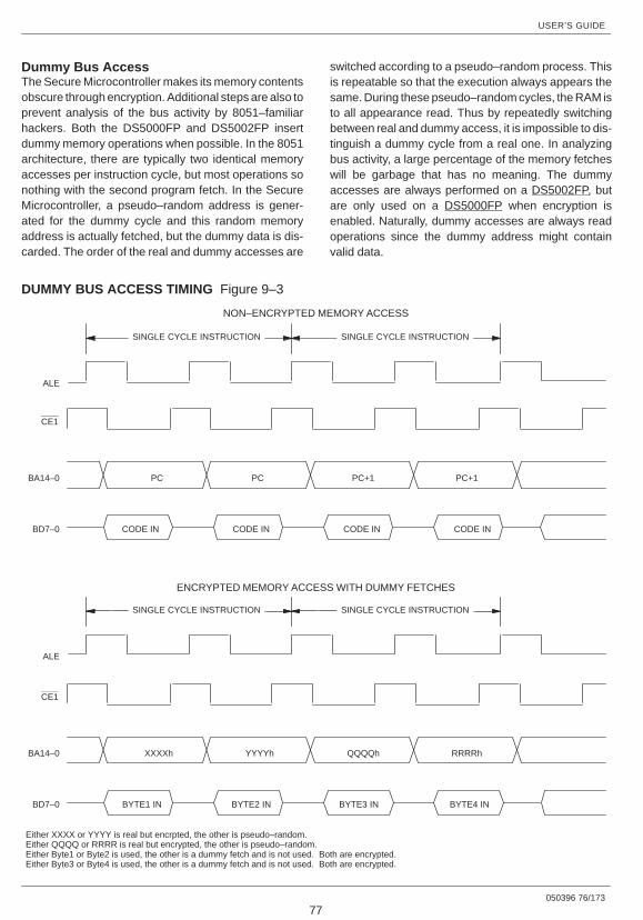
CE1
ALE
BA14–0
BD7–0
XXXXh YYYYh QQQQh RRRRh
SINGLE CYCLE INSTRUCTION SINGLE CYCLE INSTRUCTION
ENCRYPTED MEMORY ACCESS WITH DUMMY FETCHES
Either XXXX or YYYY is real but encrpted, the other is pseudo–random.Either QQQQ or RRRR is real but encrypted, the other is pseudo–random.Either Byte1 or Byte2 is used, the other is a dummy fetch and is not used. Both are encrypted.Either Byte3 or Byte4 is used, the other is a dummy fetch and is not used. Both are encrypted.
BYTE1 IN BYTE2 IN BYTE3 IN BYTE4 IN
USER’S GUIDE
050396 76/173
77
Dummy Bus AccessThe Secure Microcontroller makes its memory contentsobscure through encryption. Additional steps are also toprevent analysis of the bus activity by 8051–familiarhackers. Both the DS5000FP and DS5002FP insertdummy memory operations when possible. In the 8051architecture, there are typically two identical memoryaccesses per instruction cycle, but most operations sonothing with the second program fetch. In the SecureMicrocontroller, a pseudo–random address is gener-ated for the dummy cycle and this random memoryaddress is actually fetched, but the dummy data is dis-carded. The order of the real and dummy accesses are
switched according to a pseudo–random process. Thisis repeatable so that the execution always appears thesame. During these pseudo–random cycles, the RAM isto all appearance read. Thus by repeatedly switchingbetween real and dummy access, it is impossible to dis-tinguish a dummy cycle from a real one. In analyzingbus activity, a large percentage of the memory fetcheswill be garbage that has no meaning. The dummyaccesses are always performed on a DS5002FP, butare only used on a DS5000FP when encryption isenabled. Naturally, dummy accesses are always readoperations since the dummy address might containvalid data.
DUMMY BUS ACCESS TIMING Figure 9–3
CE1
ALE
BA14–0
BD7–0
PC PC PC+1 PC+1
CODE IN CODE IN CODE IN CODE IN
SINGLE CYCLE INSTRUCTION SINGLE CYCLE INSTRUCTION
NON–ENCRYPTED MEMORY ACCESS

USER’S GUIDE
050396 77/173
78
On–chip Vector RAMA 48–byte RAM area is incorporated inside theDS5000FP and DS5002FP. This area maps to the first48 locations of program memory to store reset andinterrupt vectors. Any other data stored in the first 48locations will be contained in this Vector RAM. The prin-cipal reason for the Vector RAM is that the reset andinterrupt vectors are known logical addresses in the8051 family. Thus an attacker could force a reset orinterrupt and discover the encrypted address gener-ated by the Secure Microcontroller. By storing theseVectors in on–chip RAM, it is impossible to observesuch relationships. Although it is very unlikely that anapplication program could be deciphered by observingthe vector addresses, the Vector RAM eliminated thispossibility. Note that the dummy accesses discussedabove also occur while the Vector area is beingaccessed.
The Vector RAM is automatically loaded with the resetand interrupt vectors during Bootstrap Loading. Thisfeature is transparent to operation and no action isrequired to use it. However, considering the Vector areafeature can improve overall system security. As men-tioned above, the Vector RAM is instantaneouslydestroyed in the event of an unlock (also by a self–de-struct on DS5002FP). Since it is hidden and subject todestruction, the 48 bytes are the most secure memory ina system. Thus the most critical constants can also bestored there. This is an ideal location for storing DESkeys for applications involving data encryption such aselectronic funds transfer.
The Vector RAM is always used on a DS5002FP. Thedata stored between logical location 00h and 30h will beloaded into and executed for the Vector RAM. This datawill not be duplicated in NV RAM accessed by the Byte–wide bus. The operation of DS5000FP Vector RAM isthe same, but only when the encryption feature isenabled. When a DS5000FP has not had an EncryptionKey loaded, the Vector RAM is left unused.
Self–Destruct InputThe Self–Destruct Input (SDI) is an active high input pinthat is used to clear the security lock on a DS5002FP inresponse to an external event. The SDI is intended to beused with external tamper detection circuitry. It can beactivated by an active high signal with or without operat-
ing power applied to the VCCI pin. Activation of the SDIpin instantaneously clears the Security Lock initiatingthe sequence of events described above. In addition,power is momentarily removed from all Byte–wide businterface signals including the VCCO pin, resulting inloss of data by the external RAM. Address and datalines are also pulled low to remove any excess chargethat could help retain data in that RAM. The SDI pin isdeglitched so that a 2 µs pulse is required to activate it.However, this pin is sensitive so it should be grounded ifnot used. It is only available on the DS5002FP andDS2252FP products.
Microprobe/Die Top CoatingThe DS5002FPM is provided with a special top–layercoating that is designed to prevent a microprobe attack.The coating is implemented with a second layer of metalon the microcontroller die. This metal will result in ashort circuit of critical functions if probing is attempted.The probing action destroys the data that is secret.Also, security circuits and Vector RAM derive theirpower from this screen. Therefore they will be de–pow-ered if the top coating is removed, also destroying thesecret data. In this event, any critical data stored on–chip will be destroyed and off–chip data is rendered use-less.
Random Number GeneratorAs mentioned above, the DS5002FP incorporates ahardware random number generator used by the Boot-strap Loader to generate Encryption Keys. The Ran-dom Number Generator is not a security circuit perse,but it is available to the application and can be used toimprove the overall system security. Random numbershave numerous applications with respect to security.For example, to prevent an attacker from developing ahistogram of code execution, the Random NumberGenerator could be used to decide how long to spend onparticular activities. The random number is created8 bits at a time. They are obtained by the applicationcode at SFR location 0CFh. The random number takes160 µs to develop. Reading a byte from register 0CFhwill start the generation of another random number.After the random number is read, another will be avail-able approximately 160 µs later. The RNR bit(RPCTL.7; 0D8h) will be set to a logic 1 each time a newnumber is available. If the random number is read priorto RNR being set, the value will be 00.
USER’S GUIDE
050396 78/173
79
Security Summary by PartThe preceding information outlined each of the securityfeatures. Their inclusion in various parts is shown in thetable at the beginning of this chapter. For completeness,the following is a summary description of security fea-tures for each part in the Secure Microcontroller Family.
DS5000FP / DS5000(T) / DS2250(T)The DS5000 is the second generation of a microcontrol-ler with security. The first is an earlier version of DS5000circa 1988, now obsolete. The DS5000 incorporates acombination of real–time memory encryption and Secu-rity Lock. The memory encryption is optional however.To invoke the encryption, the user must select a 48–bitEncryption Key using the Bootstrap Loader. A user thenloads the memory which will be automatically encryptedusing this Key. After the memory is loaded and verified,the DS5000 can be locked. Locking the micro preventsan attacker from using the Bootstrap Loader to decryptand dump the memory contents. Unlocking the DS5000destroys the Encryption Key and Vector RAM. VectorRAM is 48 bytes of secret storage on–chip. It is used tohold reset and interrupt vectors as well as any applica-tion values than must be hidden. In addition to encrypt-ing the memory, the DS5000 generates dummy buscycles to obscure the actual program flow. Dummycycles appear to be actual memory fetches but are notactually used inside the microcontroller. Also funda-mental to the security of a DS5000 is its basis on RAM.This allows all security features to be changed fre-quently. The strategy is that an attacker must spend along time breaking into the DS5000, but the user cansimply change system security at any time. Thus anystolen information has a very limited lifetime.
DS5001FP / DS2251TThe DS5001 is a newer product than the DS5000, buthas less security. It is useful in systems that need a largememory, but that provide sufficient physical security forall needs. The DS5001 incorporates a Security Lock.
This is used to prevent the Bootstrap Loader fromdumping memory. Once locked, the Bootstrap Loadercan not access the memory. Unlocking the DS5001causes the Bootstrap Loader to write over the NV RAM.The RAM nature of the DS5001 product allows a user tovary security frequently and to manually destroy it if nec-essary.
DS5002FP / DS2252(T)The DS5002 adopts the memory and I/O improvementsof the DS5001 and improves on the security of theDS5000. It is a high security version of the DS5001. Thisdevice is intended for maximum security and hasnumerous improvements to the DS5000. The security isalways enabled on a DS5002. Thus an attacker can notcharacterize the security and the user can not forget toenable the security. The DS5002 follows a similarscheme of memory encryption and Security Lock. TheDS5002 encryptor is a superior algorithm using a 64–bitEncryption Key. In addition, the Key is managed by theDS5002. Using the Bootstrap Loader, each part gener-ates a random number for its 64–bit Key prior to loadingmemory. Leaving and re–entering the Bootstrap loadercauses the DS5002 to select a new number as a poten-tial Key. Any subsequent memory access with theLoader causes the new Key to be installed. Like theDS5000, the DS5002 also uses dummy bus access andVector RAM to further hide memory bus activity. TheSecurity Lock of a DS5002 is similar in nature to theDS5000. Once locked, the DS5002 Bootstrap Loaderdoes not have access to memory. Unlocking theDS5002 destroys the Encryption Key and Vector RAM.The NV RAM accessed by the Byte–wide bus is alsomanually erased under Bootstrap Loader control. TheDS5002 provides an external method to clear the Secu-rity Lock using its Self–Destruct Input (SDI). Thiscauses the erasure of the Key and Vector RAM and alsoremoves power from the NV RAM. The DS5002FPMprovides a internal metal microprobe shield to preventmicroprobing of the die.

USER’S GUIDE
050396 79/173
80
APPLICATION: ADVANCED SECURITYTECHNIQUESThe Secure Microcontroller family has been used fornumerous applications requiring security. Different lev-els of security are required depending on the sensitivityof the application and the value of the protected informa-tion. As mentioned above, the goal of the microcontrol-ler security is to make stealing the protected informationmore difficult than the information is worth. This taskactually has two pieces. First, the Secure Microcontrol-ler makes attack difficult. This is combined with theuser’s physical security to make information retrievaldifficult. The second part is to make the protectedinformation less valuable. To this end, the NV RAMnature allows a user to frequently alter the firmwarebased security aspects of the system. Thus if the criticalinformation changes before the security can be broken,the information that is actually retrieved will be worth-less.
To assess the security of a system, the total imple-mentation must be examined. The DS5000FP orDS5002FP provide a high level of security, but theuser’s firmware can accidentally defeat some features.Below are a sampling of implementation issues that willmake the DS5000FP or DS5002FP more difficult tocrack. There are also suggestions on making a systemmore secure using external circuits.
Avoid Clear TextThe encryption algorithms used by DS5000FP orDS5002FP are generally adequate to prevent analysiswhen combined with well developed code. However, theencryption is defeated to some extent if the user storestext that appears on a display in encrypted form. Thisgives the pirate a starting point to look for the clear text inencrypted storage and analyze the encryption algo-rithm. The “data answer” is already known. If clear text isrequired, then preferably store it in nonencryptedmemory. If this is impractical, then disperse it so that it ishard to find. Avoid at all costs reading the clear text frommemory then immediately displaying it. This is a suremeans to identify the encrypted values of the text for theattacker.
Avoid CRC or ChecksumRunning a checksum on power up provides the piratewith a sequential listing of the addresses in encryptedform. Therefore the attacker has a great advantage indeciphering the Address Encryptor. Preferably avoid a
checksum. If one is needed, then check the minimumamount of memory and perform the check in non–se-quential fashion.
Avoid Long Straight Runs of CodeA common coding practice is to run numerous sequen-tial operations. This is common knowledge and shouldbe avoided. The pirate can use this in the same way as achecksum process. It provides a sequential listing ofencrypted addresses and assists with analysis of theaddress encryption.
Use JumpsTo address the prior problem, jumps are advised. Thesecan be jumps for no reason other than to space outstraight runs of code. However, using jumps also pro-vides several other techniques to make bus analysismore difficult. As an example, the code can jump intoVector RAM. While in this area, dummy access willoccur on the bus.
Use Random valuesThe Random Number Generator of the DS5002FP canbe used to make a pirate’s task more difficult. When timeis available, the software should perform randomactions at random time intervals. As an example, theRandom Number Generator can be used to select atimer interrupt value. Thus the microprocessor will beinterrupted at random intervals making characterizationvery difficult. Software can elect to out of Vector RAM fora random period of time. Also as discussed above, themicroprocessor generates dummy RAM reads whenpossible. However, it can not generate dummy writes.However the user’s code can. Random numbers can bewritten to address that are known to be unused. If this isdone while the microprocessor is visibly performing ameaningful task, it will make analysis very difficult.
Vector RAMAs mentioned above, the Vector RAM can be used formany things beside vectors. This is the most securestorage in the system. It resides on–chip behind tamperprotection. Thus it is useful for storing the most sensitivedata. Thus even an attacker could break the encryption,this information would still be secret. For EFT or similarapplications, this is a good location for the storage ofDES keys. Since DES is a public algorithm, the realprotection is keeping the DES key secret. As this is only8 bytes, it fits well within the Vector RAM.
USER’S GUIDE
050396 80/173
81
Change CodePerhaps most importantly, the user should reprogramportions of the Secure Microcontroller that deal with se-curity. For example, if the microprocessor is performingDES, the user can change DES keys. Any security sys-tem can be broken with enough time and resources. Byaltering the security features, this threat can be mini-mized.
External CircuitsA variety of external circuits can support secure opera-tion. For example, the DS2400 is a unique 48–bit SiliconSerial Number. If it is installed with the microprocessor, itcan be read when the system is first powered up, then
stored inside the Secure Microcontroller. This serializesthe system. If the software ever finds a different serialnumber (or missing number) from the stored one, it canrefuse to work. This would mean that the microproces-sor had been moved.
Tamper ProtectionUsing a variety of tamper sensors in conjunction with theDS5002 makes the system very difficult to crack. Thesecircuits vary from simple switches to light, temperature,pressure, or oxygen sensors. When the physical secu-rity is violated, the SDI pin is activated and the memorycontents are destroyed.
USER’S GUIDE
050396 81/173
82
SECTION 10: RESET CONDITIONSReset SourcesThe Secure Microcontroller family is designed to pro-vide proper reset operation with a minimum of externalcircuitry. In fact, for may applications, external reset cir-cuitry is not required. The possible sources of reset areas follows:
a) Power On (operating voltage applied to VCC)
b) No VLI Power On
c) External RST pin
d) Watchdog Timeout
Certain actions are taken in all cases where a reset hasbeen issued. Whenever any type of reset is executed,the ALE and PSEN quasi–bidirectional pins are confi-gured as inputs. In addition, an internal reset line (IRST)is active continuously until the condition which is caus-ing the reset has been removed. IRST will then go inac-tive and execution of the application program will begin.Special Function Registers are initialized during resetas shown in Table 10–1.
Figure 10–1 is a summary of the bits that indicate thesource of the most recent reset. Operational detailswhich are unique to the different sources of reset arediscussed below:
RESET STATUS BITS Figure 10–1
PCON.6: POR
“Power On Reset”: Indicates that the previous reset was initiated during a Power On.
Initialization: Cleared to a 0 whenever a Power On Reset occurs; remains unchanged onother types of resets. Must be set to a 1 by software.
Read Access: Can be read normally anytime.
Write Access: Can be written only by using the Timed Access register.
PCON.4: WTR
“Watchdog Timer Reset”: Set to a 1 when a timeout condition of the Watchdog Timer occurs. Clearedto a 0 immediately following a read operation.
Initialization: Set to a 1 on a Watchdog Timeout Reset. Remains unchanged on any othertype of reset.
Read Access: Read normally anytime.
Write Access: Not writable.
PCON.2: EWT
“Enable Watchdog Timer”: The Watchdog Timer is enabled if EWT is set to a 1 and is disabled if EWT iscleared to a 0. This is not normally considered a status bit but is convenientfor detecting a No VLI reset condition.
Initialization: Cleared to a 0 on a No–VLI Power On Reset. Remains unchanged duringother types of reset.
Read Access: May be read normally anytime.
Write Access: Writable only by using the Timer Access register.
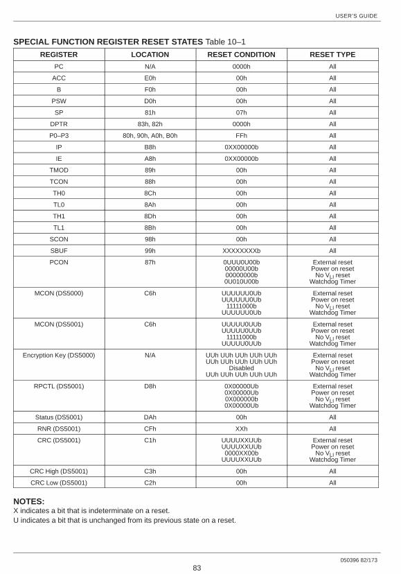
USER’S GUIDE
050396 82/173
83
SPECIAL FUNCTION REGISTER RESET STATES Table 10–1
REGISTER LOCATION RESET CONDITION RESET TYPE
PC N/A 0000h All
ACC E0h 00h All
B F0h 00h All
PSW D0h 00h All
SP 81h 07h All
DPTR 83h, 82h 0000h All
P0–P3 80h, 90h, A0h, B0h FFh All
IP B8h 0XX00000b All
IE A8h 0XX00000b All
TMOD 89h 00h All
TCON 88h 00h All
TH0 8Ch 00h All
TL0 8Ah 00h All
TH1 8Dh 00h All
TL1 8Bh 00h All
SCON 98h 00h All
SBUF 99h XXXXXXXXb All
PCON 87h 0UUU0U00b00000U00b00000000b0U010U00b
External resetPower on reset
No VLI resetWatchdog Timer
MCON (DS5000) C6h UUUUUU0UbUUUUUU0Ub
11111000bUUUUUU0Ub
External resetPower on reset
No VLI resetWatchdog Timer
MCON (DS5001) C6h UUUUU0UUbUUUUU0UUb
11111000bUUUUU0UUb
External resetPower on reset
No VLI resetWatchdog Timer
Encryption Key (DS5000) N/A UUh UUh UUh UUh UUhUUh UUh UUh UUh UUh
DisabledUUh UUh UUh UUh UUh
External resetPower on reset
No VLI resetWatchdog Timer
RPCTL (DS5001) D8h 0X00000Ub0X00000Ub0X000000b0X00000Ub
External resetPower on reset
No VLI resetWatchdog Timer
Status (DS5001) DAh 00h All
RNR (DS5001) CFh XXh All
CRC (DS5001) C1h UUUUXXUUbUUUUXXUUb0000XX00b
UUUUXXUUb
External resetPower on reset
No VLI resetWatchdog Timer
CRC High (DS5001) C3h 00h All
CRC Low (DS5001) C2h 00h All
NOTES:X indicates a bit that is indeterminate on a reset.U indicates a bit that is unchanged from its previous state on a reset.
USER’S GUIDE
050396 83/173
84
Power On ResetThe Secure Microcontroller family provides an internalPower On Reset capability which requires no externalcomponents. When voltage is applied to the VCC pinfrom a power off condition, the device automatically per-
forms an internal reset sequence to prepare the proces-sor for execution of the application software. The tradi-tional capacitor reset circuit should not be used.Figure 10–2 illustrates the timing associated with thePower On Reset cycle.
POWER ON RESET TIMING Figure 10–2
VCCI
VLI
VCCMIN
CLOCKOSC.
INTERNALRESET
LITHIUMCURRENT
tCSU
tPOR
This cycle begins with Power On reset delay time. Thisis generated by the internal control circuitry to allow theinternal clock oscillator to start up from its halted statethat is in effect when VCC is below VCCmin. The periodtCSU is a mechanical startup time that is dependent onthe individual crystal. The delay shown as tPOR in thefigure is generated by internal circuitry which counts atotal of 21,504 (1.792 ms @ 12 MHz) clock oscillator pe-riods before it allows the internal reset line to be re-leased. The purpose of this delay is to allow time for theclock frequency to stabilize.
The Power On Reset delay is not the total amount oftime which must pass before execution can begin in theapplication from the initial application of VCC voltage.First the power supply slew rate is required for VCC torise from 0V to the VCCmin threshold shown inFigure 10–2. Next, operation with a crystal is partly me-chanical and some time is required to get the mass of
the crystal into vibrational motion. The user should con-sult the crystal vendor for a start–up time specification.
When a Power On Reset cycle is in progress, the exter-nal RST pin has no effect on internal operation. Oncecontrol of the processor is transferred to the user’s pro-gram, a hardware reset may be issued externally via theRST pin.
A Power On Reset causes special initialization to beperformed on the Special Function Registers as shownin Table 10–1.
The distinguishing action taken during a Power On Re-set is that the POR bit is cleared in order to indicate thata Power On Reset has just occurred. All other controlbits which are initialized according to the type of resetare left unchanged from their previous condition.
USER’S GUIDE
050396 84/173
85
No–VLI Power On ResetDuring a Power On Reset cycle, a test is automaticallyperformed by the internal control circuitry to measurethe voltage of the lithium power source. This test deter-mines whether or not the voltage (VLI) is above the mini-mum level required (VLImin) to insure that the nonvolatileareas can be maintained in the absence of VCC. If thevoltage is found to be above the required level, then nospecial initialization is performed. If it is below the re-quired level, then the Special Function Registers are ini-tialized during the reset as shown in Table 10–1 for aNo–VLI reset.
The additional initialization can be summarized as fol-lows:
The POR bit (PCON.6) is cleared to indicate that a Pow-er On Reset has just occurred.
The Watchdog Timer is disabled by writing a 0 into theEWT bit (PCON.2).
The Partition Address bits (PA3–0) are set to all 1’s. Inaddition, the Range function is set to select a 32K byteaddress space for the RAM.
On a DS5000, the Encryption Key and software encryp-tion operation are disabled.
Finally, the Security Lock bit is cleared to 0.
External ResetFor applications which require an external reset capabil-ity, a reset pin (RST) is provided with a Schmitt Triggerinput. This input may be used to force a reset conditionany time when the micro is executing the applicationprogram or when it is in either the Idle or Stop modes.Reset is initiated by holding the RST pin active (high) for
a minimum time of two machine cycles (24 clock oscilla-tor periods). If the reset was initiated from Stop mode,the rising edge will result in an internally–generatedPower On Reset time (tPOR) which is required for the os-cillator to start and for the clock frequency to stabilize.
All of the control bits that are initialized according to thetype of reset within the Special Function registers areleft unchanged from their previous condition followingan External Reset. Note, an RC circuit should not beused on the reset pin to generate a power–on reset.
Watchdog Timer ResetThe on–chip Watchdog Timer is provided as a methodof restoring proper software operation in the event thatsoftware control is lost. The Watchdog Timer is enabledvia the EWT bit (PCON.2). This bit can only be written byusing the Timed Access function.
Once the Watchdog Timer is initialized, an internal resetwill be issued if the software fails to reset the timer viathe RWT bit (IP.7) at least once before it reaches itstimeout condition. The timeout period is equal to122,880 machine cycles. If a 12 MHz crystal is used asthe time base element, this give a timeout period of122.88 milliseconds. In order to reset the WatchdogTimer in the application software, the RWT bit must bewritten with a 1 using the Timed Access procedure. TheWatchdog Timer is also reset following any other type ofreset.
When a Watchdog Timer reset occurs, special initializa-tion is performed on the Special Function Registers asshown in Table 10–1.
The distinguishing action taken during this type of resetis that the WTR status flag is set to indicated that aWatchdog Timer Reset has just occurred.
USER’S GUIDE
050396 85/173
86
APPLICATION: RESET ROUTINE EXAMPLELike the 8051, Dallas Semiconductor Microcontrollerswill begin execution at address 0000h. This is the ResetVector, followed by other vector locations used for inter-rupts. These are discussed in the section covering inter-rupt operation. Since there are only three memory loca-tions dedicated to the Reset Vector, the user willtypically insert a jump statement to a more convenientmemory address. This will be the reset routine. It can lieany where in the 64K bytes of program memoryaddressed by the device. A common choice is location
0030h. Thus at location 0000h, the user would use theinstruction SJMP 30h. This instruction requires twobytes, so it easily fits in the available space. At the loca-tion of the reset routine, the user places instructions thatinitialize the microprocessor and any external hardwarespecific to the application. This note describes theoperations that are typically done and shows someexample code.
The following functions are typically initialized in auser’s reset routine:
MEMORY INTERRUPTS TIMERS/SERIAL PROTECTION
Partition Power–fail Timer setup Watchdog Timer
Current Memory Map External Timer for baud–rates POR
Data Pointer Serial Port Serial Port
Timer
Memory MapThe most critical and most overlooked initialization isthat of the memory map. Several of these functions arenonvolatile and are not cleared during a reset. Thosethat are cleared could leave the microprocessor in anundesirable state. Therefore, the user should eitherverify the correctness of the memory map or simply set itproperly following each reset. An example of how thememory map could be incorrect on reset is as follows.
The user typically sets the Partition, Range, etc., duringBootstrap Loading. In the course of operating however,the user may temporarily move the Partition to alter a
lookup table. If while the Partition is moved, a resetshould occur, the Partition will remain in the temporaryposition unless corrected.
In developing the reset routine, the user should carefullynote the reset state of each critical bit. For example,when using the ECE2 on a DS5000FP, note that it is notaltered on reset. On a DS5001FP, the PES bit is clearedon a reset. Thus a DS5000T that is accessing the Real–time Clock when a reset occurs will still be pointing theCE2 space after reset. The DS2251T user that isaccessing the RTC when a reset occurs will start in thenormal memory configuration.
USER’S GUIDE
050396 86/173
87
A code example that initializes the memory map is asfollows. It assumes that the DS5000FP user requires a
Partition of 5800h. A DS5001FP using the same codewould use a Partition of B000h.
MCON EQU 0C6hOrg 00h
SJMP Start
Org 30hStart :
MOV TA, #0AAh ;TimedMOV TA, #55h ; AccessORL MCON, #02h ;Set PAA – DS5000 ONLYMOV MCON, #0B8h ;Set Partition to 5800 on DS5000, B000h on DS5001MOV TA, #0AAh ;Timed – DS5000 ONLYMOV TA, #55h ; Access – DS5000 ONLYANL MCON, #0FDh ;Clear PAA – DS5000 ONLY
Another common memory requirement is the initializa-tion of the Data Pointer. When using NV RAM to storedata, this pointer must be moved to the Partitionaddress (in a partitionable configuration). Thus if thePartition is set to 5800h, the DPTR should be set to5800h to start. Once data has been saved in NV RAM,the DPTR should be saved in a known, nonvolatile loca-tion so that is can be restored on a reset.
InterruptsAfter a reset, all interrupts are disabled. Therefore theuser must enable individual interrupts that are needed.
The global interrupt enable must also be activated. Anyinterrupt needing a higher priority must be selected assuch. The following code example shows the enablingof individual interrupts. A user would combine theappropriate bits as needed by the application. In thisapplication example, the serial port is given a high prior-ity interrupt.
ORG 00hSJMP Start
Org 30h Start :
ORL PCON, #08h ;Enable Power–fail Warning by setting EPFWSETB PS ;Set Serial Port Interrupt to High PrioritySETB ES ;Enable Serial Port InterruptSETB ET1 ;Enable Timer 1 InterruptSETB EX1 ;Enable External Interrupt 1SETB ET0 ;Enable Timer 0 InterruptSETB EX0 ;Enable External Interrupt 0
SETB EA ; Globally enable interrupts
USER’S GUIDE
050396 87/173
88
TimersThe microprocessor disables timer activity (excludingthe Watchdog) and serial port communication on a re-set. Therefore, each timer must be setup and enabledas part of the reset routine. The serial port mode mustalso be initialized if used. This is covered in detail in theUser’s Guide section on Timers and Serial I/O respec-
tively. Shown here is an example of Timer and SerialPort setup. In this example, Timer 0 is set up to generatea 10 ms interrupt. Timer 1 is setup to generate 9600baud for the serial port. The serial port is set up forasynchronous communication with a PC (mode 1). Acrystal frequency of 11.0592 MHz is assumed.
ORG 00hSJMP Start
Org 30h Start :
SETB PS ;Set Serial Port Interrupt to High PrioritySETB ES ;Enable Serial Port InterruptSETB ET0 ;Enable Timer 0 InterruptMOV TMOD, #00100001b ;Select Timer 1 mode 2 – 8 bit auto–reload,
; Timer 0 mode 1 – 16 bit manual reloadMOV TH1, #0FDh ;Setup 9600 baudMOV TL1, #00h ; ” ”MOV TH0, #0DBh ;Select a 10 ms count. 9216 counts = 10 msMOV TL0, #0FFh ; 9216d counts = 2400h counts (FFFFh–2400h =
; DBFFh); Timer 0 ISR must reload DBFFh manually
MOV SCON, #01010011b ;Select Serial Port mode 1,; TXD and RXD interrupts active
MOV TCON, #01010000b ;Enable the operation of both TimersSETB EA ;Globally enable interrupts
ProtectionThe microprocessor provides protection from transientsthrough a built in power–fail/power–on reset and Watch-dog Timer. Each of these functions should be initialized
by the user as part of the reset routine. The followingcode demonstrates the set up for a user that will supportthe Watchdog function.
TA EQU 0C7h
ORG 00hSJMP Start
Org 30hStart :
MOV TA, #0AAh ;TimedMOV TA, #55h ; AccessORL IP, #80h ;Set RWT to restart the Watchdog Timer
MOV TA, #0AAh ;TimedMOV TA, #55h ; AccessORL PCON, #44h ;Set POR (PCON.6) bit for power on reset detect
; and enable Watchdog Timer by setting EWT (PCON.2)
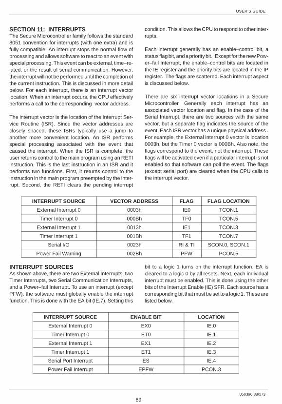
USER’S GUIDE
050396 88/173
89
SECTION 11: INTERRUPTSThe Secure Microcontroller family follows the standard8051 convention for interrupts (with one extra) and isfully compatible. An interrupt stops the normal flow ofprocessing and allows software to react to an event withspecial processing. This event can be external, time–re-lated, or the result of serial communication. However,the interrupt will not be performed until the completion ofthe current instruction. This is discussed in more detailbelow. For each interrupt, there is an interrupt vectorlocation. When an interrupt occurs, the CPU effectivelyperforms a call to the corresponding vector address.
The interrupt vector is the location of the Interrupt Ser-vice Routine (ISR). Since the vector addresses areclosely spaced, these ISRs typically use a jump toanother more convenient location. An ISR performsspecial processing associated with the event thatcaused the interrupt. When the ISR is complete, theuser returns control to the main program using an RETIinstruction. This is the last instruction in an ISR and itperforms two functions. First, it returns control to theinstruction in the main program preempted by the inter-rupt. Second, the RETI clears the pending interrupt
condition. This allows the CPU to respond to other inter-rupts.
Each interrupt generally has an enable–control bit, astatus flag bit, and a priority bit. Except for the new Pow-er–fail Interrupt, the enable–control bits are located inthe IE register and the priority bits are located in the IPregister. The flags are scattered. Each interrupt aspectis discussed below.
There are six interrupt vector locations in a SecureMicrocontroller. Generally each interrupt has anassociated vector location and flag. In the case of theSerial Interrupt, there are two sources with the samevector, but a separate flag indicates the source of theevent. Each ISR vector has a unique physical address .For example, the External interrupt 0 vector is location0003h, but the Timer 0 vector is 000Bh. Also note, theflags correspond to the event, not the interrupt. Theseflags will be activated even if a particular interrupt is notenabled so that software can poll the event. The flags(except serial port) are cleared when the CPU calls tothe interrupt vector.
INTERRUPT SOURCE VECTOR ADDRESS FLAG FLAG LOCATION
External Interrupt 0 0003h IE0 TCON.1
Timer Interrupt 0 000Bh TF0 TCON.5
External Interrupt 1 0013h IE1 TCON.3
Timer Interrupt 1 001Bh TF1 TCON.7
Serial I/O 0023h RI & TI SCON.0, SCON.1
Power Fail Warning 002Bh PFW PCON.5
INTERRUPT SOURCESAs shown above, there are two External Interrupts, twoTimer Interrupts, two Serial Communication Interrupts,and a Power–fail Interrupt. To use an interrupt (exceptPFW), the software must globally enable the interruptfunction. This is done with the EA bit (IE.7). Setting this
bit to a logic 1 turns on the interrupt function. EA iscleared to a logic 0 by all resets. Next, each individualinterrupt must be enabled. This is done using the otherbits of the Interrupt Enable (IE) SFR. Each source has acorresponding bit that must be set to a logic 1. These arelisted below.
INTERRUPT SOURCE ENABLE BIT LOCATION
External Interrupt 0 EX0 IE.0
Timer Interrupt 0 ET0 IE.1
External Interrupt 1 EX1 IE.2
Timer Interrupt 1 ET1 IE.3
Serial Port Interrupt ES IE.4
Power Fail Interrupt EPFW PCON.3
USER’S GUIDE
050396 89/173
90
External InterruptsThe two external interrupts are INT0 and INT1. Theycorrespond to P3.2 and P3.3 respectively. These pinsbecome interrupts when the respective interrupt isenabled. Otherwise, they are simply port pins. No otherspecial action is required. Each pin is sampled once permachine cycle when the interrupts are enabled. INT0 isenabled by setting the EX0 bit to a logic 1. INT1 isenabled by setting the EX1 bit to a logic 1. These bits arelocated at IE.0 and IE.2 respectively. The external inter-rupts each have a status flag that indicates that thecondition has occurred. The flags are IE0 at TCON.1and IE1 at TCON.3. These flags are set to a logic 1when the interrupt condition occurs. They are clearedwhen the CPU calls to the appropriate interrupt vector.
The external interrupts can be programmed to respondto falling–edge or low–level activation. IT0 (TCON.0)and IT1 (TCON.2) control the edge/level nature of INT0and INT1 respectively. When ITn is a logic 0, theassociated interrupt is low–level activated. This causesthe IEn flag to be set for as long as the INTn pin remainsa logic 0. The interrupt (if enabled) will remain active dur-ing this period. Note that the level interrupt is notlatched. Thus the pin must be held in a low state until theISR can be activated. If the INTn pin is brought to a logichigh prior to beginning the ISR, there will be no interrupt.If the INTn is left at a logic low after the RETI instructionof the ISR, another interrupt will be activated after oneinstruction is executed.
Setting the ITn bit to a logic 1 causes the external inter-rupt to be edge activated. This causes the device todetect a falling edge on the INTn pin. This edge condi-tion is latched until the interrupt is serviced. Thus inedge mode, the INTn pin can go from a logic 1 to a logic0, then back to a logic 1 and the interrupt will still beactive. After the falling–edge has been detected, theINTn pin is subsequently ignored until after the ISR iscompete. The edge detector is actually a “pseudo–edge” detector. Since the pin is actually sampled, thecondition must be a logic high for at least one machinecycle and logic low for at least one machine cycle inorder to guarantee recognition of the falling edge. TheIEn flag is automatically cleared when the interrupt isserviced.
Timer InterruptsThe Secure Microcontroller, like the 8051, has two inter-nal timers. These timers can each generate an interruptwhen the value in the timer registers overflows. When
the Timer 0 overflows, the TF0 flag is set to al logic 1.Likewise for the TF1 flag with respect to Timer 1. TF0 islocated at TCON.5 and TF1 is located at TCON.7.These flags indicate the overflow condition. If the corre-sponding timer interrupt is desired, then ET0 at IE.1 andET1 at IE.3 must be set to a logic 1 respectively. Whenset, the timer overflow will cause an interrupt to theappropriate vector location. If the interrupt is active, theflag will automatically be cleared by the CPU.
Serial Port InterruptsThe on–chip serial port generates an interrupt wheneither a word is received or a word is transmitted. Theinterrupt is effectively a logical OR of the two conditions.Each condition has its own flag. The flags operateregardless of whether the interrupt has been enabled.RI is located at SCON.0 and represents a serial wordreceived. TI is located at SCON.1 and represents aserial word transmitted. Each flag is set to a logic 1 toindicate an active state. Since there are two flags for oneinterrupt, these flags are used by the ISR to determinethe cause of the interrupt. The flags must be cleared bysoftware to clear the interrupt condition. The serial inter-rupt is activated by setting the ES bit at IE.4 to a logic 1.
Power–fail Warning InterruptThe Secure Microcontroller family adds a new interruptto the standard 8051 collection. It is used in conjunctionwith the power monitor and nonvolatile memory. Duringa power down or brown out, as VCC is falling, the SecureMicrocontroller can generate an early warning Power–fail Interrupt (PFW). This allows the software to savecritical data prior to entering a reset condition. Since thenonvolatile RAM is not affected by a reset, this data iseffectively saved. Software can use the PFW to save thecurrent routine, current data, shut off external functions,or simply to enter a known region of memory for thepower down.
The PFW is enabled by setting the EPFW bit at PCON.3to a logic 1. The Power–fail Warning flag (PFW) islocated at PCON.5. When ever VCC drops below theVPFW voltage threshold, the PFW flag will be set to alogic 1. This flag will be cleared when read by software.If the voltage is still below the VPFW, the flag will againbe set immediately. This will occur regardless ofwhether the interrupt is enabled. The VPFW voltage isdifferent for each member of the Secure Microcontrollerfamily. Check the electrical specifications for details.Note that the PFW interrupt is not controlled by the EA
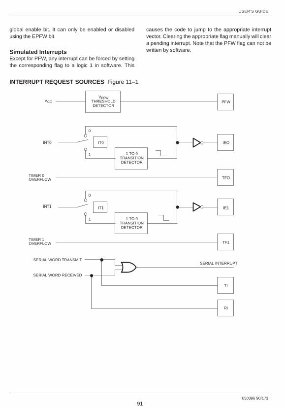
USER’S GUIDE
050396 90/173
91
global enable bit. It can only be enabled or disabledusing the EPFW bit.
Simulated InterruptsExcept for PFW, any interrupt can be forced by settingthe corresponding flag to a logic 1 in software. This
causes the code to jump to the appropriate interruptvector. Clearing the appropriate flag manually will cleara pending interrupt. Note that the PFW flag can not bewritten by software.
INTERRUPT REQUEST SOURCES Figure 11–1
PFW
IEO
TFO
IE1
TF1
0
1
0
1
VPFWTHRESHOLDDETECTOR
1 TO 0TRANSITIONDETECTOR
1 TO 0TRANSITIONDETECTOR
IT0
IT1
VCC
TIMER 0OVERFLOW
TIMER 1OVERFLOW
INT0
INT1
TI
RI
SERIAL WORD TRANSMIT
SERIAL WORD RECEIVED
SERIAL INTERRUPT
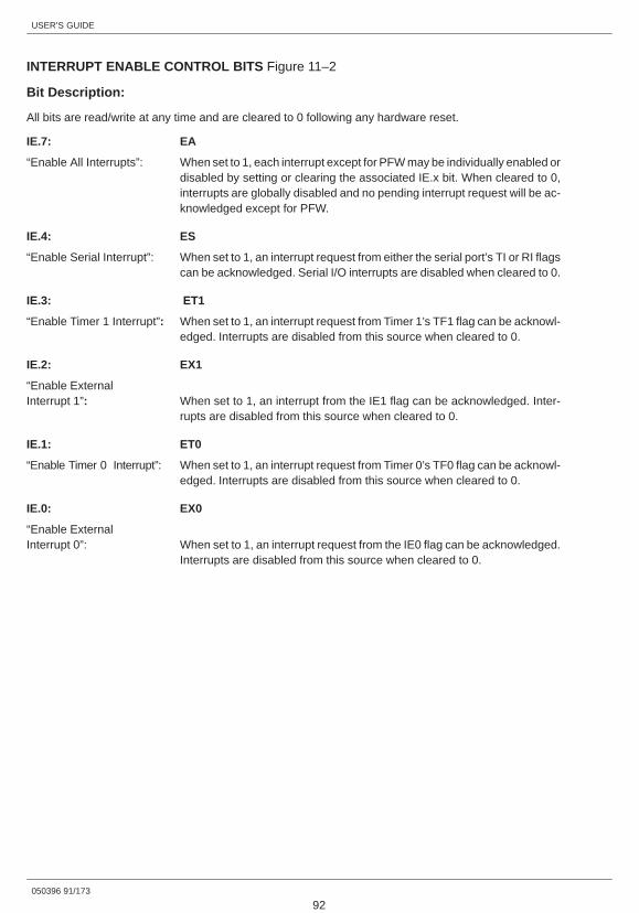
USER’S GUIDE
050396 91/173
92
INTERRUPT ENABLE CONTROL BITS Figure 11–2
Bit Description:
All bits are read/write at any time and are cleared to 0 following any hardware reset.
IE.7: EA
“Enable All Interrupts”: When set to 1, each interrupt except for PFW may be individually enabled ordisabled by setting or clearing the associated IE.x bit. When cleared to 0,interrupts are globally disabled and no pending interrupt request will be ac-knowledged except for PFW.
IE.4: ES
“Enable Serial Interrupt”: When set to 1, an interrupt request from either the serial port’s TI or RI flagscan be acknowledged. Serial I/O interrupts are disabled when cleared to 0.
IE.3: ET1
“Enable Timer 1 Interrupt”: When set to 1, an interrupt request from Timer 1’s TF1 flag can be acknowl-edged. Interrupts are disabled from this source when cleared to 0.
IE.2: EX1
“Enable External Interrupt 1”: When set to 1, an interrupt from the IE1 flag can be acknowledged. Inter-
rupts are disabled from this source when cleared to 0.
IE.1: ET0
“Enable Timer 0 Interrupt”: When set to 1, an interrupt request from Timer 0’s TF0 flag can be acknowl-edged. Interrupts are disabled from this source when cleared to 0.
IE.0: EX0
“Enable External Interrupt 0”: When set to 1, an interrupt request from the IE0 flag can be acknowledged.
Interrupts are disabled from this source when cleared to 0.

USER’S GUIDE
050396 92/173
93
INTERRUPT PRIORITIESThe Secure Microcontroller provides a three priorityinterrupt scheme. Multiple priority levels allow higherpriority sources to interrupt lower priority ISRs. ThePower–fail Warning Interrupt automatically has thehighest priority if enabled. The remaining interrupts canbe programmed by the user to either high or low priority.The priority scheme woks as follows. The ISR for a lowpriority source can be interrupted by a high prioritysource. A low priority ISR can not be interrupted byanother low priory source. Neither can a high priorityISR be interrupted by a another high priority source. ThePFW source will interrupt any ISR if activated.
In the case of simultaneous interrupt requests, the mi-crocontroller has a natural scheme to arbitrate. First, ifhigh and low priority interrupt requests are receivedsimultaneously, then the high priority source will beserviced. If two or more requests from equal prioritysources are received, the following natural priorityscheme will be used to arbitrate.
Each interrupt priority is determined by an individual bitas shown below. Setting the appropriate bit to a logic 1will cause that interrupt to be high priority.
PRIORITY FLAG INTERRUPT SOURCE
1 PFW Power–fail Warning
2 IE0 External Interrupt 0
3 TF0 Timer 0 Interrupt
4 IE1 External Interrupt 1
5 TF1 Timer 1 Interrupt
6 RI+TI Serial I/O Interrupt
INTERRUPT PRIORITY CONTROL BITS Figure 11–3
Bit Description:
All bits are read/write at any time and are cleared to 0 following any hardware reset.
IP.4: PS
“Serial Port Priority”: Programs Serial Port interrupts for high priority when set to 1. Low priority isselected when cleared to 0.
IP.3: PT1
“Timer 1 Priority”: Programs Timer 1 interrupt for high priority when set to 1. Low priority is se-lected when cleared to 0.
IP.2: PX1
“Ext. Int. 1 Priority”: Programs External Interrupt 1 for high priority when set to 1. Low priority isselected when cleared to 0.
IP.1: PT0
“Timer 0 Priority”: Program Timer 0 interrupt for high priority when set to 1. Low priority is se-lected when cleared to 0.
IP.0: PX0
“Ext. Int. 0 Priority”: Programs External Interrupt 0 for high priority when set to 1. Low priority isselected when cleared to 0.
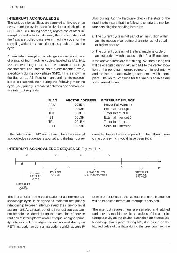
USER’S GUIDE
050396 93/173
94
INTERRUPT ACKNOWLEDGEThe various interrupt flags are sampled an latched onceevery machine cycle, specifically during clock phaseS5P2 (see CPU timing section) regardless of other in-terrupt related activity. Likewise, the latched states ofthe flags are polled once every machine cycle for thesampling which took place during the previous machinecycle.
A complete interrupt acknowledge sequence consistsof a total of four machine cycles, labeled as IA1, IA2,IA3, and IA4 in Figure 11–4. The various interrupt flagsare sampled and latched once every machine cycle,specifically during clock phase S5P2. This is shown inthe diagram as IA1. If one or more pending interrupt reg-isters are latched, then during the following machinecycle (IA2) priority is resolved between one or more ac-tive interrupt requests.
Also during IA2, the hardware checks the state of themachine to insure that the following criteria are met be-fore servicing the pending interrupt:
a) The current cycle is not part of an instruction withinan interrupt service routine of an interrupt of equalor higher priority.
b) The current cycle is not the final machine cycle ofan instruction which accesses the IP or IE registers.
If the above criteria are met during IA2, then a long callwill be executed during IA3 and IA4 to the vector loca-tion of the pending interrupt source of highest priorityand the interrupt acknowledge sequence will be com-plete. The vector locations for the various sources aresummarized below.
FLAG VECTOR ADDRESS INTERRUPT SOURCEPFW 002BH Power Fail WarningIE0 0003H External Interrupt 0TF0 000BH Timer Interrupt 0IE1 0013H External Interrupt 1TF1 001BH Timer Interrupt 1RI+TI 0023H Serial I/O Interrupt
If the criteria during IA2 are not met, then the interruptacknowledge sequence is aborted and the interrupt re-
quest latches will again be polled on the following ma-chine cycle (which would have been IA3).
INTERRUPT ACKNOWLEDGE SEQUENCE Figure 11–4
IA1 IA2 IA3 IA4
INTERRUPTSERVICEROUTINE
LONG CALL TOVECTOR ADDRESS
POLLINGCYCLEINTERRUPT
LATCHED(S5P2)
INTERRUPTGOES
ACTIVE
The first criteria for the continuation of an interrupt ac-knowledge cycle is designed to maintain the priorityrelationship between interrupts and their priority levelassignment. As a result, pending interrupt sources can-not be acknowledged during the execution of serviceroutines of interrupts which are of equal or higher prior-ity. Interrupt acknowledges are not allowed during anRETI instruction or during instructions which access IP
or IE in order to insure that at least one more instructionwill be executed before an interrupt is serviced.
The interrupt request flags are sampled and latchedduring every machine cycle regardless of the other in-terrupt activity on the device. Each time an attempt ac-knowledge takes place during IA2, it is based on thelatched value of the flags during the previous machine

USER’S GUIDE
050396 94/173
95
cycle. If the interrupt acknowledge does not take placefor one of the reasons cited above, the request flag willbecome subsequently inactive and the interrupt willhave been lost and will not be serviced.
When an interrupt request is acknowledged, a long callis executed to the interrupt vector location and the2–byte return address is pushed onto the stack. In addi-tion, an internal flag is set which indicates to the hard-ware the interrupt source that is being serviced. Execu-tion then proceeds from the interrupt vector location. Atthe conclusion of the interrupt service routine, an RETIinstruction should be performed to return control to themain program. The RETI performs the same action as aRET instruction in terms of its operation on the stack andthe Program Counter. In other words, two bytes of returnaddress are popped off the stack and loaded into theProgram Counter. However, the RETI performs the
additional operation of clearing the interrupt–in–serviceflag to inform the hardware that a service routine is nolonger in progress. Therefore, an RETI should alwaysbe used to terminate an interrupt service routine. Failureto do so would indicate that the interrupt was still beingserviced.
Higher priority interrupts, which are enabled, can inter-rupt lower priority interrupts. According to this rule, ahigher priority interrupt could become pending just priorto machine cycle IA3 during an interrupt acknowledge ofa lower priority interrupt. This would cause the hardwareto vector to the higher priority service routine during thetwo machine cycles just after the long call to the lowerpriority interrupt so that no instruction within the lowerpriority interrupt service routine would have beenexecuted.

EXTERNALADDRESSCONTROL
VCCADDRESS/DATA
POWERDOWN
PORT0.n
INTERNALDATA BUS
WRITEENABLE
READENABLE
READLATCH/PIN
D Q
Q
USER’S GUIDE
050396 95/173
96
SECTION 12: PARALLEL I/O
OVERVIEWThe Secure Microcontroller provides four 8–bit bidirec-tional ports for general purpose I/O functions. Each portpin is bit and byte addressable using four SFRs that con-trol the respective port latch. Each bit has an associatedlatch (accessed via SFR), input buffer circuit, and outputdriver circuit. Ports 0, 2, and 3 also have alternate func-tions that can be used in place of general I/O. All of theSFR latches for the parallel port pins are written with 1’sduring a hardware reset. Figure 12–1 illustrates func-tional circuit diagrams for bits within each of the four I/Oports. Port 1 has no alternate function; it is always avail-able for parallel I/O functions.
Ports 0 and 2 can serve as a multiplexed ExpandedMemory bus for applications needing memory mappedI/O. In the DS5001/2FP the Ports 0 and 2 can also serveas a slave RPC interface to a host microprocessor.
Port 3 pins each have individual, optional functions de-scribed below. Enabling the optional function by writinga 1 to the associated latch bit in the Port 3 SFR automati-cally converts the I/O pin into its alternate function. Forexample, enabling the serial port automatically convertsP3.0 and P3.1 into the RXD and TXD function. Alternatefunctions pins and general I/O pins can be enabled inde-pendent of each other. Enabling selected pins to per-form their alternate function leaves the other as bitaddressable I/O pins.
PIN NAME FUNCTIONP3.7 RD Expanded Data Memory Read StrobeP3.6 WR Expanded Data Memory Write StrobeP3.5 T1 Timer/Counter 1 InputP3.4 T0 Timer/Counter 0 InputP3.3 INT1 External Interrupt 1 InputP3.2 INT0 External Interrupt 0 InputP3.1 TXD Serial Port Transmit DataP3.0 RXD Serial Port Receive Data
In many cases it may be desirable to use a combinationof pure I/O and alternate function pins on port 3. For ex-ample, a user may decide to use the serial port andINTO pins, leaving 5 pins available for use as generalpurpose I/O (assuming P3.6 and P3.7 are not beingused to access external memory). SETB and CLR com-mands can be used to access the general I/O pins with-
out any effect on the pins being used in their alternatefunction. If the MOV command is used to write to port 3,however, software must always write a logic 1 to the pinsthat are being used in their alternate function. Failure todo so will disturb their function, resulting in serial portdata corruption or disabling of the alternate function inthe case of other pins.
PORT 0 FUNCTIONAL CIRCUITRY Figure 12–1
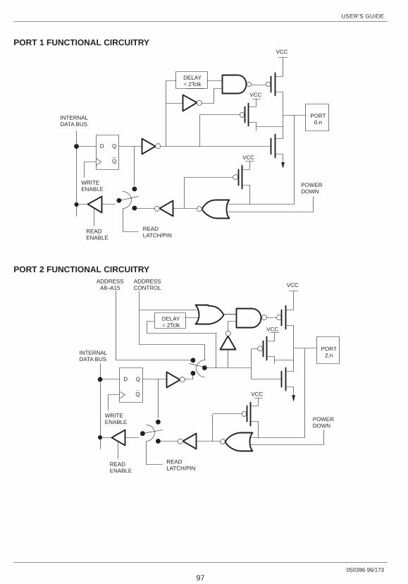
USER’S GUIDE
050396 96/173
97
PORT 1 FUNCTIONAL CIRCUITRYVCC
POWERDOWN
PORT0.n
INTERNALDATA BUS
WRITEENABLE
READENABLE
READLATCH/PIN
D Q
VCC
VCC
DELAY= 2Tclk
Q
PORT 2 FUNCTIONAL CIRCUITRY
VCC
POWERDOWN
PORT2.n
WRITEENABLE
READENABLE
READLATCH/PIN
D Q
VCC
VCC
DELAY= 2Tclk
ADDRESSCONTROL
ADDRESSA8–A15
INTERNALDATA BUS
Q
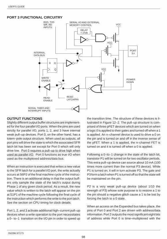
USER’S GUIDE
050396 97/173
98
PORT 3 FUNCTIONAL CIRCUITRY
VCC
POWERDOWN
PORT3.n
WRITEENABLE
READENABLE
READLATCH/PIN
D Q
VCC
VCC
SERIAL I/O AND EXTERNALMEMORY CONTROL
RXD, TXDWR, RDINPUTS
INTERNALDATA BUS
Q
DELAY= 2Tclk
SERIAL TIMER ANDINTERRUPT INPUTS
OUTPUT FUNCTIONSSlightly different output buffer structures are implement-ed for the four parallel I/O ports. When the pins are usedstrictly for parallel I/O, ports 1, 2, and 3 have internalweak pull–up devices. Port 0, on the other hand, has atotem–pole output structure. When used as outputs, allport pins will drive the state to which the associated SFRlatch bit has been set except for Port 0 which will onlydrive low. Port 0 requires a pull–up to drive high whenused as parallel I/O. Port 0 functions as true I/O whenused as the multiplexed address/data bus.
When an instruction is executed that writes a new valueto the SFR latch for a parallel I/O port, the write actuallyoccurs at S6P2 of the final machine cycle of the instruc-tion. There is an additional delay in that the output buff-ers only sample the state of the latch’s output duringPhase 1 of any given clock period. As a result, the newvalue which is written to the latch will appear on the pinat S1P1 of the machine cycle following the final cycle ofthe instruction which performs the write to the port latch.See the section on CPU timing for clock details.
Port 1, 2, and 3 activate additional high–current pull–updevices when a write operation to the port necessitatesa 0– to–1 transition on the I/O pin in order to speed up
the transition time. The structure of these devices is il-lustrated in Figure 12–2. The pull–up structure is com-prised of three pFET devices which are turned on whena logic 0 is applied to their gates and turned off when a 1is applied. An n–channel device is used to drive a 0 onthe pin and is turned on and off in the inverse sense ofthe pFET. When a 1 is applied, the n–channel FET isturned on and it is turned off when a 0 is applied.
Following a 0–to–1 change in the state of the latch bit,transistor P1 will be turned on for two oscillator periods.This extra pull–up device can source about 10 mA (100times more current than the normal P3 device). WhileP1 is turned on, it will in turn activate P3. The gate andP3 form a latch when P1 is turned off so that the state willbe maintained on the pin.
P2 is a very weak pull–up device (about 1/10 thestrength of P3) whose sole purpose is to restore a 1 tothe pin should a negative glitch cause a 1 to be lost byforcing the latch to a 0 state.
When an access on the Expanded bus takes place, thepins of Port 0 and Port 2 are driven with address/datainformation. Port 2 outputs the most significant eight bitsof address while Port 0 is time–multiplexed with the
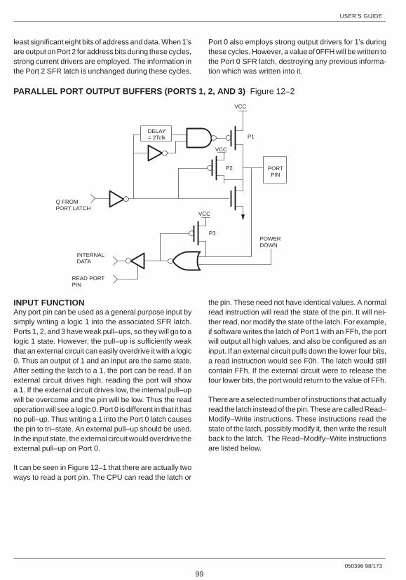
USER’S GUIDE
050396 98/173
99
least significant eight bits of address and data. When 1’sare output on Port 2 for address bits during these cycles,strong current drivers are employed. The information inthe Port 2 SFR latch is unchanged during these cycles.
Port 0 also employs strong output drivers for 1’s duringthese cycles. However, a value of 0FFH will be written tothe Port 0 SFR latch, destroying any previous informa-tion which was written into it.
PARALLEL PORT OUTPUT BUFFERS (PORTS 1, 2, AND 3) Figure 12–2
DELAY= 2Tclk
VCC
VCC
PORTPIN
POWERDOWN
VCC
P1
P2
P3
Q FROMPORT LATCH
INTERNALDATA
READ PORTPIN
INPUT FUNCTIONAny port pin can be used as a general purpose input bysimply writing a logic 1 into the associated SFR latch.Ports 1, 2, and 3 have weak pull–ups, so they will go to alogic 1 state. However, the pull–up is sufficiently weakthat an external circuit can easily overdrive it with a logic0. Thus an output of 1 and an input are the same state.After setting the latch to a 1, the port can be read. If anexternal circuit drives high, reading the port will showa 1. If the external circuit drives low, the internal pull–upwill be overcome and the pin will be low. Thus the readoperation will see a logic 0. Port 0 is different in that it hasno pull–up. Thus writing a 1 into the Port 0 latch causesthe pin to tri–state. An external pull–up should be used.In the input state, the external circuit would overdrive theexternal pull–up on Port 0.
It can be seen in Figure 12–1 that there are actually twoways to read a port pin. The CPU can read the latch or
the pin. These need not have identical values. A normalread instruction will read the state of the pin. It will nei-ther read, nor modify the state of the latch. For example,if software writes the latch of Port 1 with an FFh, the portwill output all high values, and also be configured as aninput. If an external circuit pulls down the lower four bits,a read instruction would see F0h. The latch would stillcontain FFh. If the external circuit were to release thefour lower bits, the port would return to the value of FFh.
There are a selected number of instructions that actuallyread the latch instead of the pin. These are called Read–Modify–Write instructions. These instructions read thestate of the latch, possibly modify it, then write the resultback to the latch. The Read–Modify–Write instructionsare listed below.

USER’S GUIDE
050396 99/173
100
READ–MODIFY–WRITE INSTRUCTIONS
MNEMONIC DESCRIPTIONANL – Logical ANDORL – Logical ORXRL – Logical Exclusive ORJBC – Branch if Bit Set and Clear (bit)CPL – Complement BitINC – IncrementDEC – DecrementDJNZ – Decrement and Branch if not ZeroMOV PX.n,C – Move Carry Bit to bit n of Port XCLR PX.n – Clear bit n in Port XSETB PX.n – Set bit n in Port X
Read–Modify–Write instructions input the state of the latch rather than the pin so that the operation takes place on thevalue which was originally written to the latch by the software.
REPROGRAMMABLE PERIPHERALCONTROLLER (RPC)The Reprogrammable Peripheral Controller (RPC)mode of the DS5001FP and DS5002FP emulate the8042 slave hardware interface commonly used in IBM–compatible PCs for control of peripherals such as a key-board or a mouse device. In addition to a direct interfaceto the PC backplane bus, the device brings the advan-tages of up to 128KB of reprogrammable, nonvolatileprogram and data memory to intelligent peripheral con-trol. The nonvolatile data memory accessed by thedevice can be used for system configuration, hard disksetup parameters, or even maintenance records.
In operating as a slave controller, the device communi-cates with a host processor via three resource registers:Data Bus Buffer In (DBBIN), Data Bus Buffer Out(DBBOUT), and Status (STATUS). The host may read
data or status and write data or commands. The STA-TUS register provides information about DBBIN,DBBOUT, and user–defined flags. Both DBBIN andDBBOUT share special function register address 80Hwith Port 0. The context will determine which register isused. The STATUS register is at SFR location 0DAH.
To enable the RPC mode, the RPCON bit in the RPCTLregister (described in Figure 12–6) must be set to a 1. Atthis time, Ports 0 and 2 are reconfigured to emulate the8042 hardware interface as shown in Figure 12–3. Port0 becomes an 8–bit data bus that can connect directly toa PC data bus. Port 2 provides the control and addressinformation for the data bus. Both ports are true bidirec-tional I/O devices in this mode. Normal operation ofthese ports is suspended when RPC mode is enabled.The modified port functions are described as follows:
Port 0: D0–7 This is the 8–bit bi–directional data bus of the RPC. It can interface directly to a PC or other host.
Port 2.0: A0 Address input used to determine whether the data bus word is data or command/status.
Port 2.1: CE If a multiple RPC mode environment is required, this input can be used to select an individualDS5001 on a common bus.
Port 2.2: RD Input that allows the host to read data or status from the DBBOUT or STATUS.
Port 2.3: WR Input that allows the host to write data or commands to DBBIN.
Port 2.4: OBF Output flag that indicates to a host that the output buffer is full and should be read.
Port 2.5: IBF Output that indicates to a host that the input buffer is empty.
Port 2.6: DRQ Output that indicates to a host that a DMA is required.
Port 2.7: DACK Input that indicates to the DS5001 that the host has granted a DMA.
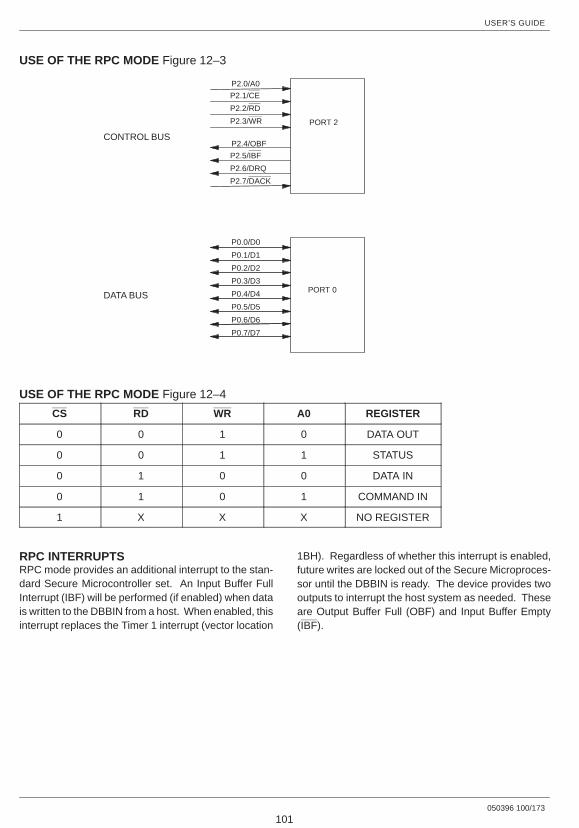
USER’S GUIDE
050396 100/173
101
USE OF THE RPC MODE Figure 12–3
P2.3/WR
P2.2/RD
P2.1/CE
PORT 2
P2.0/A0
P2.7/DACK
P2.6/DRQ
P2.5/IBF
P2.4/OBFCONTROL BUS
PORT 0
P0.0/D0
DATA BUS
P0.1/D1
P0.2/D2
P0.3/D3
P0.4/D4
P0.5/D5
P0.6/D6
P0.7/D7
USE OF THE RPC MODE Figure 12–4
CS RD WR A0 REGISTER
0 0 1 0 DATA OUT
0 0 1 1 STATUS
0 1 0 0 DATA IN
0 1 0 1 COMMAND IN
1 X X X NO REGISTER
RPC INTERRUPTSRPC mode provides an additional interrupt to the stan-dard Secure Microcontroller set. An Input Buffer FullInterrupt (IBF) will be performed (if enabled) when datais written to the DBBIN from a host. When enabled, thisinterrupt replaces the Timer 1 interrupt (vector location
1BH). Regardless of whether this interrupt is enabled,future writes are locked out of the Secure Microproces-sor until the DBBIN is ready. The device provides twooutputs to interrupt the host system as needed. Theseare Output Buffer Full (OBF) and Input Buffer Empty(IBF).
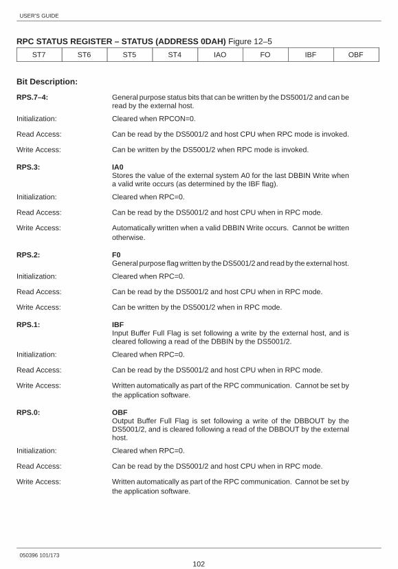
USER’S GUIDE
050396 101/173
102
RPC STATUS REGISTER – STATUS (ADDRESS 0DAH) Figure 12–5
ST7 ST6 ST5 ST4 IAO FO IBF OBF
Bit Description:
RPS.7–4: General purpose status bits that can be written by the DS5001/2 and can beread by the external host.
Initialization: Cleared when RPCON=0.
Read Access: Can be read by the DS5001/2 and host CPU when RPC mode is invoked.
Write Access: Can be written by the DS5001/2 when RPC mode is invoked.
RPS.3: IA0Stores the value of the external system A0 for the last DBBIN Write whena valid write occurs (as determined by the IBF flag).
Initialization: Cleared when RPC=0.
Read Access: Can be read by the DS5001/2 and host CPU when in RPC mode.
Write Access: Automatically written when a valid DBBIN Write occurs. Cannot be writtenotherwise.
RPS.2: F0General purpose flag written by the DS5001/2 and read by the external host.
Initialization: Cleared when RPC=0.
Read Access: Can be read by the DS5001/2 and host CPU when in RPC mode.
Write Access: Can be written by the DS5001/2 when in RPC mode.
RPS.1: IBFInput Buffer Full Flag is set following a write by the external host, and iscleared following a read of the DBBIN by the DS5001/2.
Initialization: Cleared when RPC=0.
Read Access: Can be read by the DS5001/2 and host CPU when in RPC mode.
Write Access: Written automatically as part of the RPC communication. Cannot be set bythe application software.
RPS.0: OBFOutput Buffer Full Flag is set following a write of the DBBOUT by theDS5001/2, and is cleared following a read of the DBBOUT by the externalhost.
Initialization: Cleared when RPC=0.
Read Access: Can be read by the DS5001/2 and host CPU when in RPC mode.
Write Access: Written automatically as part of the RPC communication. Cannot be set bythe application software.
USER’S GUIDE
050396 102/173
103
RPC PROTOCOLData is written to the microprocessor by the host CPUand is placed in the DBBIN. At this time, the IBF flag isset in the RPC Status Register. If enabled by the IBI bitin the RPCTL register, an IBI interrupt will occur. No fur-ther updates of the DBBIN will be allowed until the bufferis read by the microprocessor. Once read, the IBF flagwill be cleared. When the DBBOUT is written to by themicroprocessor, the OBF is set in the RPC Status Reg-ister (STATUS). No future writes are allowed until theDBBOUT is read by the external host. The OBF iscleared when such a read takes place.
The RPC mode provides a simple interface to a hostprocessor. In general, four control bits specify theoperation to be performed. This works as shown in Fig-ure 12–3.
These conditions provide the basis of a complete slaveinterface. The protocol for such communications mightoperate as follows:
1. Host processor reads STATUS.
2. If DBBIN is empty (IBF=0), host writes a data or com-mand word to DBBIN.
3. If DBBOUT is full (OBF=1), host reads a word fromDBBOUT.
4. RPC detects IBF flag via interrupt or polling. Inputdata or command word is processed.
5. RPC recognizes OBF=0, and writes a new word toDBBOUT.
Timing diagrams in RPC AC electrical specificationsillustrate the operation of the RPC mode bus transfers.A DBBOUT read places the contents of DBBOUT on thedata bus and clears OBF. A STATUS register readplaces the contents of the STATUS register on the databus. A write to DBBIN causes the contents of the databus to be transferred to the DBBIN, and the IBF flag(STATUS) is set. A command write operates in thesame way. The DS5001FP or DS5002FP can deter-mine whether the write was data or command byexamining the IA0 bit in the STATUS register. This bitwill be equal to the A0 input of the most recent valid hostwrite operation.
DMA OPERATIONIf DMA transfers are required, the RPC mode can sup-port them. DMA transfers are initiated by setting theDMA bit in the RPCTL register. The DRQ output is de–asserted at this time. DRQ can be asserted by writing a1 to the DRQ line (P2.6) from software. The host CPUmust respond by pulling the DACK input low. Data canthen be transferred according to the user’s required pro-tocol. DMA mode can be cancelled by clearing the DMAbit, by a reset, or by clearing the RPCON bit of theRPCTL control register to leave the RPC mode.
USER’S GUIDE
050396 103/173
104
RPC CONTROL REGISTER – RPCTL (ADDRESS 0D8H) Figure 12–6
RNR – EXBS AE IBI DMA RPCON RG0
Bit Description:
RPCTL.3: IBIWhen using the RPC mode, an interrupt may be required for the Input BufferFlag. This interrupt is enabled by setting the Input Buffer Interrupt (IBI) bit.At this time, the timer 1 interrupt is disabled, and this RPC mode interruptis used in its place (vector location 1BH). This bit can be set only when theRPCON bit is set.
Initialization: Cleared on all resets, and when the RPCON bit is cleared.
Read Access: Can be read at any time.
Write Access: Can be written when RPC mode is enabled (RPCON=1).
RPCTL.2: DMAThis bit is set to enable DMA transfers when RPC mode is invoked. It canonly be set when RPCON=1.
Initialization: Cleared on all resets, and when the RPC is cleared.
Read Access: Can be read at any time.
Write Access: Can be written when RPC mode is enabled (RPCON=1).
RPCTL.1: RPCONEnable the 8042 I/O protocol. When set, Port 0 becomes the data bus, andPort 2 becomes the control signals as shown in Figure 12–3.
Initialization: Cleared on all resets.
Read Access: Can be read at any time.
Write Access: Can be written at any time.

USER’S GUIDE
050396 104/173
105
SECTION 13: PROGRAMMABLE TIMERS
FUNCTIONAL DESCRIPTIONThe Secure Microcontroller incorporates two 16–bit tim-ers called Timer 0 and Timer 1. Both can be used to gen-erate precise time intervals, measure external pulsewidths, or count externally applied pulses.
Each programmable timer operates either as a “timer”in which time periodic interrupts may be generated or asa “counter”, in which the timer register is incrementedwhen transitions are detected on an external input pin.
When a programmable timer is operating as a “timer”,the least–significant timer register is incremented onceevery machine cycle or at 1/12 the frequency of theclock oscillator. When a 12 MHz crystal is used, the reg-ister will be incremented once every 1 µs.
When “counter” operation is selected, the least–signifi-cant timer register is incremented each time that a1–to–0 transition is detected on the corresponding inputpin that may be assigned for the timer (T0 for Timer 0, T1for Timer 1). These pins are the optional function of P3.4and P3.5 respectively. The timing of the “counter” modeis internally synchronized to the machine cycles. DuringS5P2 of every machine cycle, the external input pin issampled. A 1–to–0 transition is defined as a 1 detectedduring a machine cycle followed by a 0 detected in theS5P2 clock phase of the next machine cycle. The newcount value in the timer register will be present during
clock phase S3P1 of the next successive (or third) ma-chine cycle. See the section on timing for details.
The TMOD and TCON Special Function registers areused to control the initialization of the two program-mable timers. A summary of the bits contained in TMODis shown in Figure 13–1. The relevant TCON registerbits are depicted in Figure 13–2. Each Timer has fourcontrol bits associated with it including C/T, GATE, M1,and M0. C/T=1 selects counter operation and C/T=0 se-lects timer operation.
A separate GATE bit in the TMOD register is providedfor each timer. These bits enable an associated externalinterrupt input pin as a gating control for the timer orcounter function. The P3.2 (INT0) pin operates in con-junction with Timer 0 while the P3.3 (INT1) pin operateswith Timer 1. When the Timer Run bit (TRn) and GATEare both set to a 1, the timer or counter function will beenabled only during the times that the associated inter-rupt input pin is at a 1 level. When the Timer function isselected, the GATE bit provides a means of measuringthe widths of logic 1 pulses applied to the interrupt pin inunits of machine cycles. When the counter function isselected, the pulse is measured in units of 1–to–0 transi-tions detected on the external counter input pin.
Both of the programmable timers have M1,M0 controlbits in the TMOD register which are used to select one ofthe four operating modes described below.
TMOD REGISTER CONTROL BIT SUMMARY Figure 13–1
Bit Description
TMOD.7 (Timer 1);TMOD.3 (Timer 0): GATE
“Gate Control”: When set to 1 with TRns=1, timer/counter’s input count pulses will only bedelivered while a 1 is present on the INT pin. When cleared to 0, counterpulses will always be received by the timer/counter as long as TRn=1.
Initialization: Cleared to 0 on any reset.
TMOD.6 (Timer 1);TMOD.2 (Timer 0): C/T
“Counter/Timer Select”: When set to a 1, the counter function is selected for the associated program-mable timer; when cleared to 0, the timer function is selected.
Initialization: Cleared to 0 on any reset.
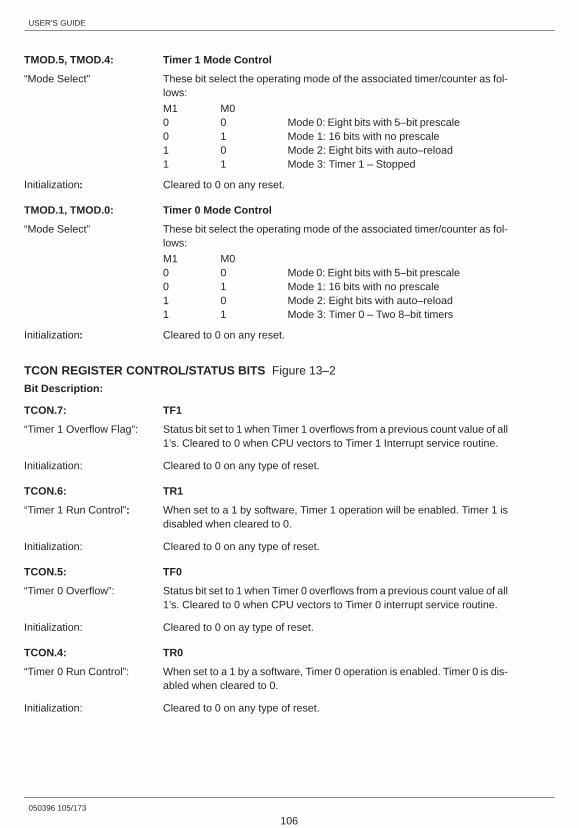
USER’S GUIDE
050396 105/173
106
TMOD.5, TMOD.4: Timer 1 Mode Control
“Mode Select” These bit select the operating mode of the associated timer/counter as fol-lows:
M1 M00 0 Mode 0: Eight bits with 5–bit prescale0 1 Mode 1: 16 bits with no prescale1 0 Mode 2: Eight bits with auto–reload1 1 Mode 3: Timer 1 – Stopped
Initialization: Cleared to 0 on any reset.
TMOD.1, TMOD.0: Timer 0 Mode Control
“Mode Select” These bit select the operating mode of the associated timer/counter as fol-lows:
M1 M00 0 Mode 0: Eight bits with 5–bit prescale0 1 Mode 1: 16 bits with no prescale1 0 Mode 2: Eight bits with auto–reload1 1 Mode 3: Timer 0 – Two 8–bit timers
Initialization: Cleared to 0 on any reset.
TCON REGISTER CONTROL/STATUS BITS Figure 13–2
Bit Description:
TCON.7: TF1
“Timer 1 Overflow Flag”: Status bit set to 1 when Timer 1 overflows from a previous count value of all1’s. Cleared to 0 when CPU vectors to Timer 1 Interrupt service routine.
Initialization: Cleared to 0 on any type of reset.
TCON.6: TR1
“Timer 1 Run Control”: When set to a 1 by software, Timer 1 operation will be enabled. Timer 1 isdisabled when cleared to 0.
Initialization: Cleared to 0 on any type of reset.
TCON.5: TF0
“Timer 0 Overflow”: Status bit set to 1 when Timer 0 overflows from a previous count value of all1’s. Cleared to 0 when CPU vectors to Timer 0 interrupt service routine.
Initialization: Cleared to 0 on ay type of reset.
TCON.4: TR0
“Timer 0 Run Control”: When set to a 1 by a software, Timer 0 operation is enabled. Timer 0 is dis-abled when cleared to 0.
Initialization: Cleared to 0 on any type of reset.

USER’S GUIDE
050396 106/173
107
Mode 0Figure 13–3 is a block diagram of a timer/counter oper-ating in Mode 0. Mode 0 configures either program-mable timer for operation as a 13–bit timer/counter. ForTimer 0, selection of Mode 0 configures bit 4 – 0 of TL0as bits 4 – 0 respectively of the 13–bit timer/counter reg-ister. In addition, bits 7 – 0 of TH0 are configured as bits12 – 5 respectively of the 13–bit timer/counter register.Bits 7 – 5 of TL0 are indeterminate and should be ig-nored when read. All of the timer/counter bits arecleared to 0 by a hardware reset. When the TR0 bit is setwith either GATE=0 or INT0=1, the 13–bit register will beincremented as each count is received. The previous
value of the 13–bit register is unchanged when the TR0bit is set to a 1 from a previous 0 condition.
When the 13–bit timer/counter reaches a value of1FFFH (all 1’s) the next count received will cause thevalue to roll over to 0000 and the TF0 flag will be set. Ad-ditionally, an interrupt will be generated if it had been en-abled.
Mode 0 operation for Timer 1 is functionally identical tothat described for Timer 0. TH1 and TL1 are used toform the 13–bit register as just described for Timer 0.Likewise, TR1, TF1, and INT1 perform the functions de-scribed for TR0, TF0, and INT0.
TIMER/COUNTER MODE 0 AND 1 OPERATION Figure 13–3
TF0 INTERRUPT
7 0
7 0
1
MU
X
MU
X
1
INVALID WHEN READ IN MODE 0
0 IF MODE 01 IF MODE 1
TH0
TL0
T0 PIN
OSC. DIVIDEBY 12
GATE
INT0 PIN
TR0
NOTE: FOR TIMER 1 OPERATION
TF0 ➞ TF1TH0 ➞ TH1TL0 ➞ TL1T0 ➞ T1TR0 ➞ TR1INT0 ➞ INT1
1 IF C/T = 10 IF C/T = 0
0
0ÏÏÏÏÏÏÏÏÏÏÏÏ

USER’S GUIDE
050396 107/173
108
Mode 1Mode 1 for both programmable timers operates in anidentical fashion described for Mode 0, except Mode 1configures a 16–bit timer/counter register. In this case,for Timer 0, TH0 contains the most significant eight bitsof the count value while TL0 holds the least significanteight bits. Timer 1 uses TH1, TL1 in an identical fashionin Mode 1. Figure 13–3 is also a diagram depicting op-eration in Mode 1 for the timer/counters.
Mode 2The selection of Mode 2 configures an 8–bit timer/counter with automatic reload of a value preset by soft-
ware. Figure 13–4 illustrates a functional block diagramof this operational mode. When Timer 0 is used inMode 2, TL0 is incremented as each count is received.When the value of 0FFH (all 1’s) is reached, TF0 will beset on the next count and the reload value held in TH0will be transferred into TL0. TH0 remains unchangeduntil it is modified by the application software.
Timer 1 operates in an identical fashion when it is set foroperation in Mode 2.
TIMER/COUNTER MODE 2 OPERATION Figure 13–4
7 0
MU
X
OSC. DIVIDEBY 12
1 IF C/T = 10 IF C/T = 0
GATE
INT0 PIN
TR0
TF0
TL0
TH0
T0
INTERRUPT
RELOAD
1
0

USER’S GUIDE
050396 108/173
109
Mode 3When Timer 0 is selected for operation in Mode 3, bothTH0 and TL0 are configured independently as an 8–bittimer/counter and as an 8–bit timer. Figure 13–5 illus-trates the function of Timer 0 for Mode 3 operation.
For Timer 0 in Mode 3, TL0 becomes an 8–bit timer/counter which is controlled by the Timer 0 control bits(TR0 and TF0) in the TMOD and TCON registers. TL0’scount input may be assigned to either the 12 tCLK signalor to the external T0 pin via C/T for Timer 0. In addition,the count input may be gated as a function of the INT0pin using Timer 0’s GATE bit in TMOD.
TH0 becomes an 8–bit timer when Mode 3 is selectedfor Timer 0. TH0’s input can only be the 12 tCLK signal.
TR1 and TF1 are assigned for use with TH0 as is the in-terrupt for Timer 1, which will be generated when TH0overflows from all 1’s.
When Timer 1 is selected for operation in Mode 3, itstops counting and holds its current value. This action isthe same as setting TR1=0. When Timer 0 is selected inMode 3, Timer 1’s control bits are stolen as describedabove. As a result, Timer 1’s functions are limited in thisMODE. It is forced to operate as a timer whose clock in-put is 12 tCLK and it cannot generate an interrupt onoverflow. In addition, it also cannot be used with theGATE function. However, it can be started and stoppedby switching it into or out of Mode 3 or it can be assignedas a baud rate generator for the serial port.
TIMER 0 MODE 3 OPERATION Figure 13–5
MU
X
GATE
INT0 PIN
OSC. DIVIDEBY 12 TR0
TR1
TH0 TL0
7 0 7 0
TF1 TF0INTERRUPTINTERRUPT
T0 PIN
1 IF C/T = 10 IF C/T = 0
0
1

USER’S GUIDE
050396 109/173
110
SECTION 14: SERIAL I/O
FUNCTION DESCRIPTIONThe Secure Microcontroller, like the 8051, includes apowerful Serial I/O (UART) port capable of both syn-chronous and asynchronous communication. The baudrate and time–base source is fully programmable. Theserial port uses P3.0 as Receive Data (RXD) and P3.1Transmit Data (TXD). Note that no special action otherthan enabling the function (i.e. writing a logic 1 to thecorresponding port pins) is required to make these pinsbecome the serial port. The serial port is capable of fullduplex operation in asynchronous mode and half–du-plex operation in synchronous mode.
The serial port consists of a receive shift register,receive buffer, transmit shift register and control logic.An incoming serial word from an external source isshifted into the receive shift register one bit at a time.Bits are shifted at the baud rate, which is programmable.The baud rate must be programmed by user’s softwareto match the incoming frequency or the serial data willbe unintelligible. Once the word is received, the serialport transfers it into the receive buffer. At this time, theserial port can receive another byte into its shift register.Once a word is received, the software should read thereceive buffer before another word is completelyreceived. The serial port will automatically transfer thenew word into the receive buffer regardless of whethersoftware has read the old value. This destroys the datathat had been present from the previous word. At 9600
baud, receiving an asynchronous word takes 1.04 ms.Thus software must read a received word within 1.04 msor it may be overwritten by another incoming word.
The transmit shift register has no buffer. Software writesinto the shift register and the word is immediately shiftedout. Thus software must wait until the serial word isshifted out before writing another to transmit. Both thereceive buffer and the transmit shift register are locatedin the SFR map. Furthermore, they reside at the sameaddress called SBUF (99h). Reading SBUF automati-cally transfers the word out of the serial receive buffer.Writing to SBUF automatically transfers a byte into thetransmit shift register. Serial Port operation is controlledvia the SCON (98h) register.
Each serial port function (receive and transmit) is capa-ble of generating an interrupt. If enabled, the receivefunction interrupts the CPU when a word has beenshifted in. This indicates that software should read thereceive buffer. The serial port will set the RI flag bit in theSCON.0 location to indicate the source of the interrupt.The serial port will also generate an interrupt when it hascompletely shifted out a word. This indicates thatanother word can be transmitted. The serial port will setthe TI flag bit at SCON.1 to indicate the source of theinterrupt. Remember that the Serial Interrupt vectors tolocation 23h regardless of the source. The ISR mustdetermine the cause of the interrupt from the flags men-tioned above.
SERIAL PORT OPERATING MODES Table 14–1
MODE SYNC/ASYNC BAUD CLOCK DATA BITS START/STOP 9TH DATA BITFUNCTION
MODE 0 SYNC 12 tCLK 8 None None
MODE 1 ASYNC Timer 1Overflow
8 1 Start
1 Stop
None
MODE 2 ASYNC 32 tCLK or 64 tCLK
9 1 Start
1 Stop
0, 1, or parity
MODE 3 ASYNC Timer 1Overflow
9 1 Start
1 Stop
0, 1, or parity
The serial port has four modes (Mode 0–3) of operationas shown in Table 14–1. Mode 0, is a synchronousmode. This means that the microcontroller serial portwill supply a clock to synchronize the data I/O shifting.One clock pulse is generated per bit. The externaldevice that is communicating with the micro must alsouse this clock. This mode is typically used with serialperipherals. Synchronous mode is generally capable of
a higher speed communication speeds than theasynchronous modes. It generates its speed as a fixedfunction of 12 microcontroller oscillator clocks per bit.
Mode 1 is a 10–bit asynchronous mode using 8–bitwords, one start bit, and one stop bit. The time base isgenerated from the Timer 1 overflow and is thereforefully programmable. A user simply loads the timer with a
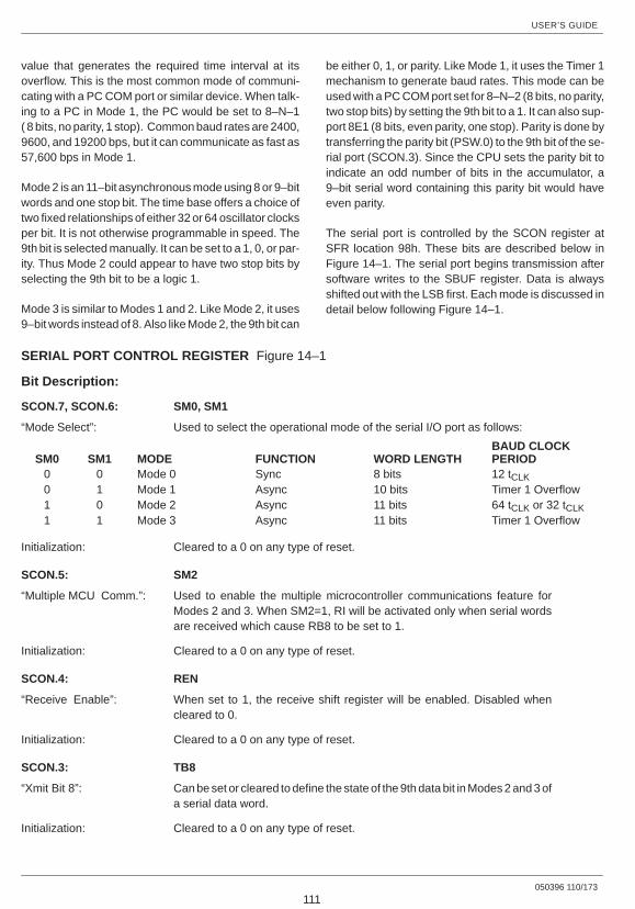
USER’S GUIDE
050396 110/173
111
value that generates the required time interval at itsoverflow. This is the most common mode of communi-cating with a PC COM port or similar device. When talk-ing to a PC in Mode 1, the PC would be set to 8–N–1( 8 bits, no parity, 1 stop). Common baud rates are 2400,9600, and 19200 bps, but it can communicate as fast as57,600 bps in Mode 1.
Mode 2 is an 11–bit asynchronous mode using 8 or 9–bitwords and one stop bit. The time base offers a choice oftwo fixed relationships of either 32 or 64 oscillator clocksper bit. It is not otherwise programmable in speed. The9th bit is selected manually. It can be set to a 1, 0, or par-ity. Thus Mode 2 could appear to have two stop bits byselecting the 9th bit to be a logic 1.
Mode 3 is similar to Modes 1 and 2. Like Mode 2, it uses9–bit words instead of 8. Also like Mode 2, the 9th bit can
be either 0, 1, or parity. Like Mode 1, it uses the Timer 1mechanism to generate baud rates. This mode can beused with a PC COM port set for 8–N–2 (8 bits, no parity,two stop bits) by setting the 9th bit to a 1. It can also sup-port 8E1 (8 bits, even parity, one stop). Parity is done bytransferring the parity bit (PSW.0) to the 9th bit of the se-rial port (SCON.3). Since the CPU sets the parity bit toindicate an odd number of bits in the accumulator, a9–bit serial word containing this parity bit would haveeven parity.
The serial port is controlled by the SCON register atSFR location 98h. These bits are described below inFigure 14–1. The serial port begins transmission aftersoftware writes to the SBUF register. Data is alwaysshifted out with the LSB first. Each mode is discussed indetail below following Figure 14–1.
SERIAL PORT CONTROL REGISTER Figure 14–1
Bit Description:
SCON.7, SCON.6: SM0, SM1
“Mode Select”: Used to select the operational mode of the serial I/O port as follows:
SM0 SM1 MODE FUNCTION WORD LENGTHBAUD CLOCKPERIOD
0 0 Mode 0 Sync 8 bits 12 tCLK0 1 Mode 1 Async 10 bits Timer 1 Overflow1 0 Mode 2 Async 11 bits 64 tCLK or 32 tCLK1 1 Mode 3 Async 11 bits Timer 1 Overflow
Initialization: Cleared to a 0 on any type of reset.
SCON.5: SM2
“Multiple MCU Comm.”: Used to enable the multiple microcontroller communications feature forModes 2 and 3. When SM2=1, RI will be activated only when serial wordsare received which cause RB8 to be set to 1.
Initialization: Cleared to a 0 on any type of reset.
SCON.4: REN
“Receive Enable”: When set to 1, the receive shift register will be enabled. Disabled whencleared to 0.
Initialization: Cleared to a 0 on any type of reset.
SCON.3: TB8
“Xmit Bit 8”: Can be set or cleared to define the state of the 9th data bit in Modes 2 and 3 ofa serial data word.
Initialization: Cleared to a 0 on any type of reset.
USER’S GUIDE
050396 111/173
112
SCON.2: RB8
“Rcv. Bit 8”: Indicates the state of the 9th data bit received while in Mode 2 or 3 operation.If Mode 1 is selected with SM2=0, RB8 is the state of the stop bit which wasreceived. RB8 is not used in Mode 0.
Initialization: Cleared to a 0 on any type of reset.
SCON.1: TI
“Xmit Interrupt”: Status bit used to signal that a word has been completely shifted out in Mode0; it is set at the end of the 8th data bit. Set when the stop bit is transmitted.
Initialization: Cleared to a 0 on any type of reset.
SCON.0: RI
“Receive Interrupt”: Status bit used to signal that a serial data word has been received andloaded into the receive buffer register. In Mode 0, it is set at the end of the 8thbit time. It is set at the mid–bit time of the incoming stop bit in all other modesof a valid received word according to the state of SM2.
Initialization: Cleared to a 0 on any type of reset.
BAUD RATE GENERATIONAs shown in Table 14–1, the baud rate clock source forthe serial I/O is determined by the selection of the oper-ating mode.
In Modes 0 and 2, the baud rate is divided down from theclock oscillator frequency by a fixed value. In Mode 0,the baud rate is 1/12 of the clock oscillator frequency, or:
Mode 0 Baud Rate � 112tCLK
In Mode 2, the baud rate is either 1/32 or 1/64 of theclock oscillator frequency. This selection is dependenton the state of the SMOD bit (PCON.7). If SMOD=0, thebaud rate will be 1/64 the clock oscillator frequency. IfSMOD=1, the baud rate is 1/32 the clock oscillator fre-quency. This can also be given as:
Mode 2 Baud Rate � 2SMOD
64X 1
tCLK
Note that 2SMOD means two to the power of SMOD.20=1, 21=2
The baud rates in Modes 1 and 3 are variable becausethey are a function of the Timer 1 overflow signal and thevalue of the SMOD bit. A general equation which de-scribes the baud rate frequency can be given as:
Mode 1, 3 Baud Rate � 2SMOD
32X 1
tT1
where, tT1 is the overflow period of Timer 1. In this ap-plication Timer 1 can be configured in either the timer orthe counter configuration. If the counter configuration isselected, then the baud rate frequency will be divideddown from an external clock source applied to the P3.3(INT1) pin. As a general guideline, the GATE bit for Tim-er 1 should be 0 if the counter function is selected in thissituation so that a continuous clock source will be avail-able for the baud generator.

USER’S GUIDE
050396 112/173
113
In most applications, Timer 1 will be configured as a tim-er which uses the internal clock oscillator frequency asits clock source. The baud rate will then be divided downfrom the time base applied to the XTAL1 and XTAL2pins. In order to provide the most flexibility, Timer 1should be programmed to operate in Mode 2 which con-
figures TL1 as an 8–bit timer which is automatically re-loaded with the value held in TH1 when its timeoutcondition is reached. This operational mode is selectedby assigning the TMOD register control bits in the fol-lowing configuration:
D7 D6 D5 D4 D3 D2 D1 D0
GATE C/T M1 M0 GATE C/T M1 M00 0 1 0 X X X X
In the configuration selected above, the baud rate for the serial port can be expressed as:
Serial I�O Mode 1, 3 Baud Rate �2SMOD
32X 1
12tCLK (256 � (TH1))
Table 14–2 lists some commonly used baud rates whichcan be derived by using Timer 1 in the timer configura-
tion described above with a 11.059 MHz crystal as thetime base.
TIMER 1 BAUD RATE GENERATION Table 14–2
BAUD RATE (BPS) 1/tCLK (MHz)SMOD
(PCON.7)TIMER 1
C/TTIMERMODE TH1
19200 11.059 1 0 2 0FDH
9600 11.059 0 0 2 0FDH
4800 11.059 0 0 2 0FAH
2400 11.059 0 0 2 0F4H
1200 11.059 0 0 2 0E8H
300 11.059 0 0 2 0A0H
When Timer 1 is used in this manner its interrupt shouldbe disabled since the timeout period is much faster thanis reasonable for interrupt response and service by theapplication software. See the application note at theend of this section.
SYNCHRONOUS OPERATION (MODE 0)Mode 0 is the synchronous operating Mode 0 of theSerial I/O Port. It is intended primarily for transferringdata to external shift registers or for communication withserial peripheral devices. The word length is eight bitson both transmit and receive. Serial data is both inputand output on the RXD pin. Both transmit and receivedata are synchronized to a clock signal which is outputon the TXD pin at the serial data rate fixed at 1/12 of thefrequency of the clock oscillator. A block diagram of theserial I/O port and timing waveforms for Mode 0 is
shown in Figure 14–2 as a reference for the followingdiscussion.
Serial data output is initiated following any instructionwhich causes data to be written to the Transmit Shiftregister located at the SBUF register address. At thetime that data is written to the Transmit Shift register, a 1is simultaneously written to the 9th bit position of theregister (D8). The internal WRSBUF signal is pulsedduring S6P2 and data is shifted out LSB first beginningat S6P2 of the next machine cycle. The contents of theTransmit Shift register are shifted to the right one posi-tion during S6P2 of every machine cycle until D7 hasbeen output. As each shift right operation is performed,a 0 is shifted into the MSB position from the left. At theend of the D7 bit time, another shift is performed at S6P2which loads the output latch of RXD with the 1 which
USER’S GUIDE
050396 113/173
114
was originally written into bit position D8. During the finalshift register operation, another 0 is shifted in from theleft so that the Transmit Shift register contains all 0’s.Also at this time, the Transmit Interrupt flag (TI) is setand a serial interrupt will be generated if enabled.
During serial data transmission in Mode 0, SHCLK is ini-tially driven low onto the TXD pin at S3 of the machinecycle when D0 is output. During the time that the dataword is shifted out, SHCLK will be low during S3, S4,and S5 and high during S6, S1, and S2 of every machinecycle.
A serial data word will be shifted into the Receive Shiftregister as soon as the condition REN=1 and RI=0 is sa-tisfied. This condition can only be initiated by a write tothe SCON register from the application software. AtS6P2 of the second machine cycle following the write toSCON, the RXD pin will be sampled and the value (D0)
will be shifted into the MSB position of the Receive Shiftregister. Seven more shifts will occur at S6P2 of subse-quent machine cycles until the entire 8–bit word hasbeen shifted into the Receive Shift register.
The SHCLK signal will be initially output low on the TXDpin starting at S3P1 of the same machine cycle in whichD0 was sampled. As in the case described above fortransmit, SHCLK will be low during S3, S4, and S5 andhigh during S6, S1, and S2 of every machine cycle.
After the last data bit (D7) has been shifted in, the controllogic will immediately load the Receive Data Buffer atthe SBUF register address with the contents of the Re-ceive Shift register. At S1P1 of the 10th machine cyclefollowing the write to SCON which initiated reception,the Receive Interrupt flag will be set and a serial inter-rupt will be generated if it has been enabled.
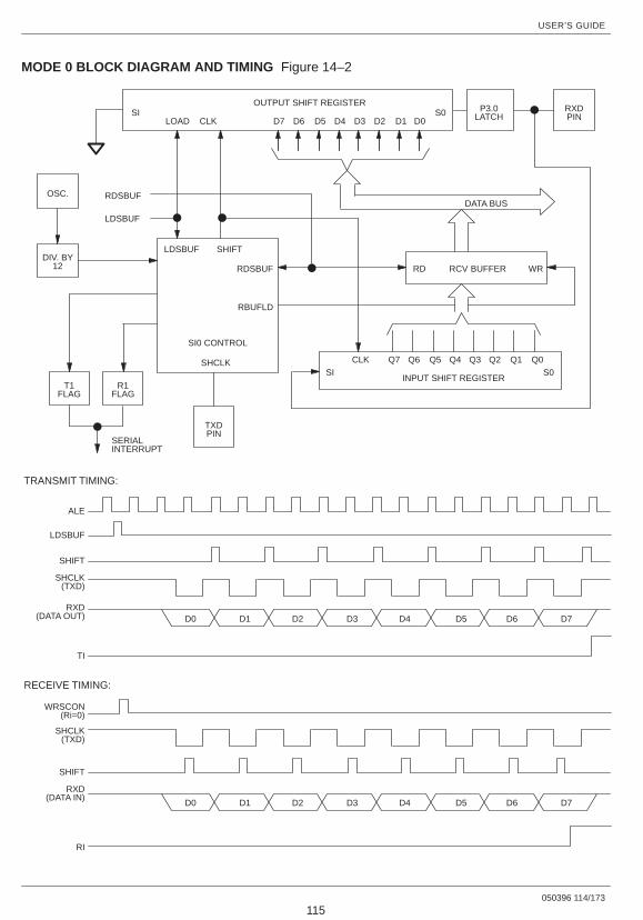
USER’S GUIDE
050396 114/173
115
MODE 0 BLOCK DIAGRAM AND TIMING Figure 14–2
T1FLAG
OUTPUT SHIFT REGISTERSI S0
LOAD CLK D7 D6 D5 D4 D3 D2 D1 D0
DATA BUS
P3.0LATCH
RXDPIN
LDSBUF
RDSBUF
R1FLAG
SERIALINTERRUPT
LDSBUF
SI0 CONTROL
SHIFT
RDSBUF
RBUFLD
RD RCV BUFFER WR
SI S0INPUT SHIFT REGISTER
CLK Q7 Q6 Q5 Q4 Q3 Q2 Q1 Q0
TXDPIN
SHCLK
DIV. BY12
OSC.
D0 D1 D2 D3 D4 D5 D6 D7
D0 D1 D2 D3 D4 D5 D6 D7
ALE
LDSBUF
SHIFT
SHCLK(TXD)
RXD(DATA OUT)
TI
WRSCON(Ri=0)
SHCLK(TXD)
SHIFT
RXD(DATA IN)
RI
TRANSMIT TIMING:
RECEIVE TIMING:
USER’S GUIDE
050396 115/173
116
ASYNCHRONOUS OPERATIONMode 1, 2, and 3 provide asynchronous, full-duplexcommunication via the Serial I/O Port. The serial dataword is either 10 or 11 bits long, depending on the modeselected. All three modes include one start bit, eightdata bits, and one stop bit. Modes 2 and 3 include anadditional, programmable 9th data bit. TXD is used forserial data output, while RXD is used for serial data in-put. In all three modes, the serial data word is both trans-mitted and received LSB first. The baud rate generatorclock pulse (BRG clock) is derived either from the Timer1 overflow output or divided directly from the clock oscil-lator frequency (of period tCLK). The following descrip-tion applies to all three of the operational modes.Figure 14–3 is a functional block diagram of the opera-tion of the serial I/O port in Mode 1 including the timingwaveforms which should be referred to in the discussionbelow.
Asynchronous serial data output begins whenever soft-ware writes to the SBUF register. When the write opera-tion occurs at the time indicated by the WRSBUF signalin the timing diagram, the contents of the 8–bit data buswill be loaded into bits D8–D1 of the Transmit Shift regis-ter. Simultaneously, a 0 will be loaded into the D0 bitposition of the shift register and a 1 will be loaded intothe Stop bit position. (D9 for Mode 1, D10 for Modes2 or 3).
During data transmission, the clocking frequency pro-vided by the output of Timer 1 is divided down by a factorof 16 by the hardware to establish the serial output bitrate. Following the write operation to the Transmit Shiftregister, the LSB will be shifted out to the output latch ofthe TXD pin at the next time the divide–by–16 counterrolls over to zero. This counter is not synchronized to themachine cycles associated with instruction execution.As a result, data transmission will commence anywherefrom 0 to 16 of the Baud Rate Generator clocks from thetime that the Transmit Shift register is written. Succes-sive bits from the Transmit Shift register will be shiftedinto the output latch of the TXD pin each time thedivide–by–16 counter rolls over to zero. As each shiftright operation is performed, a 0 is shifted into the MSBposition from the left. When the Stop bit is shifted into thelatch, the shifting operation is complete and the TI flagwill be set. A serial interrupt will be generated if it hasbeen enabled.
The Baud Rate Generator clock output is fed directlyinto the Bit Detector to perform serial data reception.
Reception begins when a valid start bit of 0 is detectedon the RXD pin. The Bit Detector will determine whenthis has occurred as follows: On each BRG clock pulse,the RXD pin will be sampled for a 1–to–0 transition.When such a transition is recognized, the Bit Detectorwill then reset its own internal divide–by–16 counter andsample the RXD pin on the 7th, 8th, and 9th BRG clocktimes following the transition. If a logic 0 level is detectedon two out of these three sample times, a valid start bit isassumed. Otherwise, the Bit Detector will reject the in-coming signal as a start bit and will repeat the processby searching for another 1–to–0 transition on RXD.
If a valid start bit is detected, the RXD pin will besampled in the middle of each successive bit time untilthe entire 10–bit or 11–bit serial word has been re-ceived. Following the detection of a valid start bit,successive bit times begin each time that the Bit Detec-tor’s divide–by–16 counter rolls over to 0. During eachbit time, the RXD pin is sampled on the 7th, 8th, and 9thBRG clock times. For the data bits, the logic level whichis read at least two out of the three sample times by theBit Detector will be the one which is shifted into the Re-ceive Shift register. Just after the logic level is detectedduring the 10th bit time, the control logic will test to see ifthe following conditions are true:
a) The previous state of RI was 0.
b) SM2=0; or if SM2=1, then if the 10th receivedbit=1.
If these conditions are met during the 10th bit time, thenthe control logic will not perform another shift, but willinstead load the contents of the Receive Shift registerinto the Receive Data Buffer, load the logic state deter-mined at the Stop bit time into the RB8 status flag (ifSM2=0), and set the RI bit. A serial interrupt will then begenerated if it the appropriate enable bits have been set.If the above conditions are not satisfied during the stopbit time, then the received word is lost.
The first condition is interpreted by the control logic tomean an “overrun” condition has been detected. Thismeans that a serial data word has been received beforesoftware read the previous word from the Receive DataBuffer. Only a hardware reset or writing logic 0 to the RIbit will clear RI. It is therefore recommended that soft-ware clear the RI bit after reading from the SBUF regis-ter. This signals the hardware that a properly receiveddata word has been processed by the application soft-
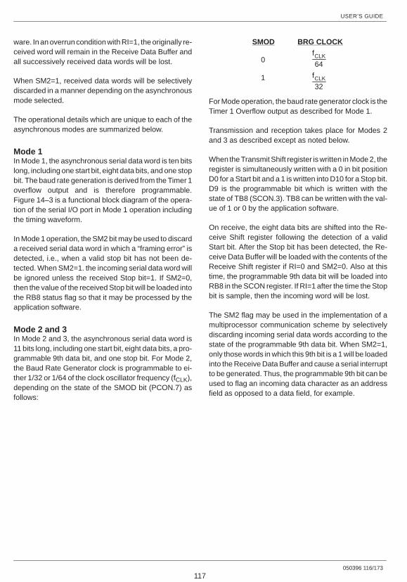
USER’S GUIDE
050396 116/173
117
ware. In an overrun condition with RI=1, the originally re-ceived word will remain in the Receive Data Buffer andall successively received data words will be lost.
When SM2=1, received data words will be selectivelydiscarded in a manner depending on the asynchronousmode selected.
The operational details which are unique to each of theasynchronous modes are summarized below.
Mode 1In Mode 1, the asynchronous serial data word is ten bitslong, including one start bit, eight data bits, and one stopbit. The baud rate generation is derived from the Timer 1overflow output and is therefore programmable.Figure 14–3 is a functional block diagram of the opera-tion of the serial I/O port in Mode 1 operation includingthe timing waveform.
In Mode 1 operation, the SM2 bit may be used to discarda received serial data word in which a “framing error” isdetected, i.e., when a valid stop bit has not been de-tected. When SM2=1. the incoming serial data word willbe ignored unless the received Stop bit=1. If SM2=0,then the value of the received Stop bit will be loaded intothe RB8 status flag so that it may be processed by theapplication software.
Mode 2 and 3In Mode 2 and 3, the asynchronous serial data word is11 bits long, including one start bit, eight data bits, a pro-grammable 9th data bit, and one stop bit. For Mode 2,the Baud Rate Generator clock is programmable to ei-ther 1/32 or 1/64 of the clock oscillator frequency (fCLK),depending on the state of the SMOD bit (PCON.7) asfollows:
fCLK
64
fCLK
32
SMOD BRG CLOCK
0
1
For Mode operation, the baud rate generator clock is theTimer 1 Overflow output as described for Mode 1.
Transmission and reception takes place for Modes 2and 3 as described except as noted below.
When the Transmit Shift register is written in Mode 2, theregister is simultaneously written with a 0 in bit positionD0 for a Start bit and a 1 is written into D10 for a Stop bit.D9 is the programmable bit which is written with thestate of TB8 (SCON.3). TB8 can be written with the val-ue of 1 or 0 by the application software.
On receive, the eight data bits are shifted into the Re-ceive Shift register following the detection of a validStart bit. After the Stop bit has been detected, the Re-ceive Data Buffer will be loaded with the contents of theReceive Shift register if RI=0 and SM2=0. Also at thistime, the programmable 9th data bit will be loaded intoRB8 in the SCON register. If RI=1 after the time the Stopbit is sample, then the incoming word will be lost.
The SM2 flag may be used in the implementation of amultiprocessor communication scheme by selectivelydiscarding incoming serial data words according to thestate of the programmable 9th data bit. When SM2=1,only those words in which this 9th bit is a 1 will be loadedinto the Receive Data Buffer and cause a serial interruptto be generated. Thus, the programmable 9th bit can beused to flag an incoming data character as an addressfield as opposed to a data field, for example.
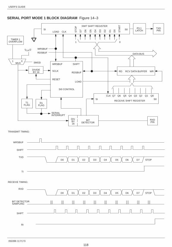
USER’S GUIDE
050396 117/173
118
SERIAL PORT MODE 1 BLOCK DIAGRAM Figure 14–3
MUX
TIMER 1OVERFLOW
1 0
T1FLAG
BITDETECTOR
RXDPIN
DIV.BY16
fCLK/2
TRANSMIT TIMING:
WRSBUF
SHIFT
TXD
TI
RXD
BIT DETECTORSAMPLING
SHIFT
RI
RECEIVE TIMING:
D0 D1 D2 D3 D4 D5 D6 D7 STOP
D0 D1 D2 D3 D4 D5 D6 D7 STOP
XMIT SHIFT REGISTERSI S0
LOAD CLK
DATA BUS
P3.1LATCH
TXDPIN
WRSBUF
RDSBUF
SMOD
DIVIDEBY 16
R1FLAG
SERIALINTERRUPT
WRSBUF
SCLK
RESET
SI0 CONTROL
SHIFT
RDSBUF
LOAD
RD RCV DATA BUFFER WR
SI S0RECEIVE SHIFT REGISTER
CLK Q7 Q6 Q5 Q4 Q3 Q2 Q1 Q0
D7
D6
D5
D4
D3
D2
D1
D0
ST
OP
STA
RT
1 0

USER’S GUIDE
050396 118/173
119
MODE2 AND 3 BLOCK DIAGRAM Figure 14–4
T1FLAG
BITDETECTOR
RXDPIN
DIV.BY16
XMIT SHIFT REGISTERSI S0
LOAD CLK
DATA BUS
P3.1LATCH
TXDPIN
WRSBUF
RDSBUF
DIVIDEBY 16
R1FLAG
SERIALINTERRUPT
WRSBUF
SCLK
RESET
SI0 CONTROL
SHIFT
RDSBUF
LOAD
RD RCV DATA BUFFER WR
SI S0RECEIVE SHIFT REGISTER
CLK Q7 Q6 Q5 Q4 Q3 Q2 Q1 Q0
TB8
Q8
RB8
BRGCLOCK
D0 D1 D2 D3 D4 D5 D6 D7 STOP
D0 D1 D2 D3 D4 D5 D6 D7 STOP
D8
TRANSMIT TIMING:
WRSBUF
SHIFT
TXD
TI
RXD
BIT DETECTORSAMPLING
SHIFT
RI
RECEIVE TIMING:
D8
D6
D5
D4
D3
D2
D1
D0
ST
OP
STA
RT
D7
1 0
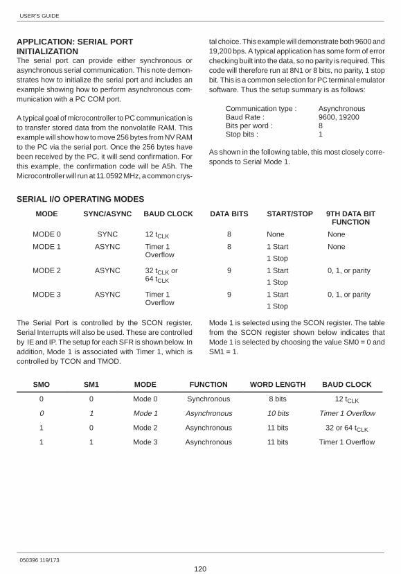
USER’S GUIDE
050396 119/173
120
APPLICATION: SERIAL PORTINITIALIZATIONThe serial port can provide either synchronous orasynchronous serial communication. This note demon-strates how to initialize the serial port and includes anexample showing how to perform asynchronous com-munication with a PC COM port.
A typical goal of microcontroller to PC communication isto transfer stored data from the nonvolatile RAM. Thisexample will show how to move 256 bytes from NV RAMto the PC via the serial port. Once the 256 bytes havebeen received by the PC, it will send confirmation. Forthis example, the confirmation code will be A5h. TheMicrocontroller will run at 11.0592 MHz, a common crys-
tal choice. This example will demonstrate both 9600 and19,200 bps. A typical application has some form of errorchecking built into the data, so no parity is required. Thiscode will therefore run at 8N1 or 8 bits, no parity, 1 stopbit. This is a common selection for PC terminal emulatorsoftware. Thus the setup summary is as follows:
Communication type : AsynchronousBaud Rate : 9600, 19200Bits per word : 8Stop bits : 1
As shown in the following table, this most closely corre-sponds to Serial Mode 1.
SERIAL I/O OPERATING MODES
MODE SYNC/ASYNC BAUD CLOCK DATA BITS START/STOP 9TH DATA BITFUNCTION
MODE 0 SYNC 12 tCLK 8 None None
MODE 1 ASYNC Timer 1Overflow
8 1 Start
1 Stop
None
MODE 2 ASYNC 32 tCLK or 64 tCLK
9 1 Start
1 Stop
0, 1, or parity
MODE 3 ASYNC Timer 1Overflow
9 1 Start
1 Stop
0, 1, or parity
The Serial Port is controlled by the SCON register.Serial Interrupts will also be used. These are controlledby IE and IP. The setup for each SFR is shown below. Inaddition, Mode 1 is associated with Timer 1, which iscontrolled by TCON and TMOD.
Mode 1 is selected using the SCON register. The tablefrom the SCON register shown below indicates thatMode 1 is selected by choosing the value SM0 = 0 andSM1 = 1.
SMO SM1 MODE FUNCTION WORD LENGTH BAUD CLOCK
0 0 Mode 0 Synchronous 8 bits 12 tCLK
0 1 Mode 1 Asynchronous 10 bits Timer 1 Overflow
1 0 Mode 2 Asynchronous 11 bits 32 or 64 tCLK
1 1 Mode 3 Asynchronous 11 bits Timer 1 Overflow

USER’S GUIDE
050396 120/173
121
SM0 = 0 and SM1 = 1 corresponds to the value SCON.7= 0 and SCON.6 = 1. In addition the since the applica-tion requires receiving data, the serial receiver must be
enabled. This is done by setting the REN bit at SCON.4to a logic 1. The remaining bits in SCON can be writtento 0. Thus the value for SCON is 01010000b or 50h.
SCON – 98hSM0 SM1 SM2 REN TB8 RB8 TI RI0 1 0 1 0 0 0 0
This application uses the serial interrupt. It serves twopurposes. First, the software knows when a byte hasbeen sent, so it knows when another can be written.Second, after the 256 bytes have been transmitted, thePC will respond. It is not know when this will occur andthe software may have other tasks to attend. Therefore
the serial interrupt will inform the microcontroller whenthe confirmation code has been received by the serialport. This example will enable only the serial Interrupt. Itwill be set for high priority since in a real system, otherinterrupts might be enabled.
IE – 0A8hEA – – ES ET1 EX1 ET0 EX01 0 0 1 0 0 0 0
To enable interrupts, the EA bit must be set. In addition,the setting the ES bit turns on the Serial Interrupt. Thusthe value 10010000b or 90h will enable serial interrupts.Note that although a timer will ultimately be used to gen-
erate serial baud rates, the timer interrupt is not used.As mentioned above, this example will use a high prior-ity for the serial interrupt. This is done as follows.
IP – 0B8hRWT – – PS PT1 PX1 PT0 PX00 0 0 1 0 0 0 0
The serial port interrupt has been set to a high priority bysetting the PS bit to a logic 1. Thus the serial port is con-figured for high priority by writing a 00010000b or 10h tothe IP register at location 0B8h.
The serial port is now configured. The only remainingtask is to set the correct baud rate. The example statedabove that the communication rate would be either 9600or 19,200 baud. To generate baud rates in Serial Mode1, the Timer 1 is used. The serial port uses the Timer 1overflow, then divides this frequency by either 16 or 32to generate the internal baud rate clock. Each time theTimer 1 value increments past 0FFh is considered anoverflow. Due to the formula used for generating baudrates shown below, the 11.0592 MHz crystal assumedfor this example generates good baud rate values. Thisis the most convenient and commonly used choice forgenerating baud rates. Other convenient values are7.3728 MHz and 1.8432 MHz.
To get 9600 bits per second, the baud rate generatormust create an interval af 1/9600 seconds = 1.0416 ms.To get 19,200 bits per second, the interval is 1/19200 =520.83 µs. Note that the timers count up, so the value
that the timer starts from must be selected to generatethe desired interval. The following values are useful:
1/11.0592 MHz = tCLK = 90.4 *10 –9
Timer runs at 12 tCLK per count = 1.085 * 10 –6
Time out = (256 – Timer start value) * 12 tCLK =(256 – Timer start value) * 1.085 * 10 –6
serial port Baud rate clock = 1/baud rate = (16or 32) * Time out
Whether 16 or 32 is used in the baud rate generator isdetermined by the SMOD bit at PCON.7. 16 is used forSMOD=1, and 32 is used for SMOD=0. This is com-monly referred to by the expression (2SMOD)/32. SinceSMOD is either 0 or 1, this value is either 1/32 or 2/32respectively.
The user selects the time–out value and the setting forSMOD to set the baud rate. This is done as follows.
Baud Rate � 2SMOD
32X 1
12tCLK * (256� TH1)
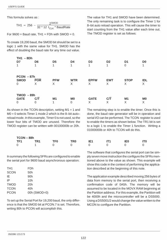
USER’S GUIDE
050396 121/173
122
This formula solves as :
TH1 � 256� 2SMOD
32 * 12 tCLK * BaudRate
For 9600 = Baud rate, TH1 = FDh with SMOD = 0.
To create 19,200 baud, the SMOD bit should be set to alogic 1 with the same value for TH1. SMOD has theeffect of doubling the baud rate for any time out value.
The value for TH1 and SMOD have been determined.The only remaining task is to configure the Timer 1 for8–bit auto reload operation. This will cause the timer tostart counting from the TH1 value after each time out.The TMOD register is set as follows:
TH1 – 8DhD7 D6 D5 D4 D3 D2 D1 D01 1 1 1 1 1 0 1
PCON – 87hSMOD POR PFW WTR EPFW EWT STOP IDL0 X X X X X X X
TMOD – 89hGATE C/T M1 M0 GATE C/T M1 M00 0 1 0 X X X X
As shown in the TCON description, setting M1 = 1 andM0 = 0 selects Timer 1 mode 2 which is the 8–bit auto–reload mode. In this example, Timer 0 is not used, so thelower four bits of TMOD are unused. Therefore theTMOD register can be written with 00100000b or 20h.
The remaining step is to enable the timer. Once this isdone, the baud rate generator will be in operation andserial I/O can be performed. The TCON register is usedto enable the timers as shown below. The TR1 bit is setto a logic 1 to enable the Timer 1 function. Writing a01000000b or 40h to TCON will do this.
TCON – 88hTF1 TR1 TF0 TR0 IE1 IT1 IE0 IT00 1 0 0 0 0 0 0
In summary the following SFRs are configured to enablethe serial port for 9600 baud asynchronous operation:
TH1 FDhSCON 50hIE 90hIP 10hTMOD 20hTCON 40hPCON 00h (SMOD=0)
To set up the Serial Port for 19,200 baud, the only differ-ence is that the SMOD bit at PCON.7 is set. Therefore,writing 80h to PCON will accomplish this.
The software that configures the serial port can be sim-ply seven move instruction the configure the SFRs men-tioned above to the value as shown. This example willshow this code in the context of performing the applica-tion described at the beginning of this note.
The application example described moving 256 bytes ofdata from memory to the serial port, then receiving aconfirmation code of 0A5h. The memory will beassumed to be located in the MOVX RAM beginning atthe Partition address. For this example, the Partition willbe 4000h and the microcontroller will be a DS5000.Using a DS5001/2 would change the value written to theMCON to configure the Partition.
USER’S GUIDE
050396 122/173
123
;This code example shows how to initialize the serial port and transmit /
; receive code as described above.
TA Equ 0C7h
MCON Equ 0C6h
Org 00h
Reset :
SJMP Start
Org 23h
Serial_ISR :
CLR RI ;Clear receive flag
CLR TI ;Clear transmit flag
RETI ;No special processing, return to application
Org 30h
Start :
MOV TA, #0AAh ;Start Timed Access
MOV TA, #55h ; finish Timed Access
MOV MCON, #88h ;Select Partition at 4000h (DS5000)
CLR RI ;Initialize receive flag
CLR TI :Initialize transmit flag
MOV SCON, #50h ;Configure Serial Port for Mode 1 and enable receiver
MOV TMOD, #20h ;Configure the Timer 1 for 8–bit auto–reload
MOV TCON, #40h ;Enable the Timer 1
MOV TH1, #0FDh ;Set Baud Rate
ANL PCON, #7Fh ;Set SMOD=0
MOV IP, #10h ;Set Serial Interrupt to high priority
MOV IE, #90h ;Globally enable interrupts and Serial Interrupt
Send :
MOV R0, #0FFh ;Set loop counter to 255
MOV DPTR, #4000h ;Put the data pointer at the beginning of data memory
Send_Loop :
MOVX A, @DPTR ;Get data byte
MOV SBUF, A ;Transmit data byte
JNB TI, $ ;Wait for serial word to be sent (interrupt)
INC DPTR ;Next byte to be sent
DJNZ R0, Send_Loop ;Decrement loop counter
Receive :
JNB RI, $ ;Wait for incoming word (interrupt)
MOV R1, SBUF ;Get received byte
CJNE R1, # 0A5h, Send ;Check for confirmation code
; and resend all data if wrong
End

XTAL2
XTAL1
GND
NC
EXT. OSC.SIGNAL
USER’S GUIDE
050396 123/173
124
SECTION 15: CPU TIMING
OSCILLATORThe Secure Microcontroller provides an on–chip oscilla-tor circuit which may be driven either by using an exter-nal crystal as a time base or from a TTL–compatibleclock signal. The oscillator circuitry provides the internalclocking signals to the on–chip CPU and I/O circuitry.
The schematic shown in Figure 15–1 illustrates the re-quired connections when using a crystal. Typically, thevalues of C1 and C2 should both be 33 pF. If a resonatoris used, C1 and C2 should be 47 pF.
XTAL1Input to the inverting oscillator amplifier and input to theinternal clock generating circuits.
XTAL2Output from the inverting oscillator amplifier. This pin isalso used to distribute the clock to other devices.
Oscillator CharacteristicsXTAL1 and XTAL2 are the input and output, respective-ly, of an inverting amplifier which can be configured foruse as an on–chip oscillator as shown in Figure 15–1.The crystal should be parallel resonant, AT cut type.
To drive the device from an external clock source,XTAL1 should be driven, while XTAL2 is left uncon-nected as shown in Figure 15–2. There are no require-ments on the duty cycle of the external clock signalsince the input to the internal clocking circuitry isthrough a divide–by–two flip–flop. However, minimumand maximum high and low times specified in the elec-trical specifications must be met to insure proper opera-tion.
CRYSTAL CONNECTION Figure 15–1
Soft Micro
XTAL1 XTAL2
33 pF 33 pF
CLOCK SOURCE INPUT Figure 15–2
USER’S GUIDE
050396 124/173
125
INSTRUCTION TIMINGThe internal clocking signals are divided to produce thenecessary clock phases, state times, and machinecycles which define the sequential execution of instruc-tions. Two clock oscillator periods define one state time.The first clock oscillator pulse period of a state time iscalled the Phase 1 clock. while the second is called thePhase 2 clock. In general, arithmetic and logical opera-tions take place during Phase 1 and internal register–to–register transfers take place during Phase 2.
A machine–cycle is composed of a total of twelve oscil-lator periods or six state times. The state times withinthe machine cycle are numbered S1 through S6. Eachclock oscillator period within the machine cycle is desig-nated according to the state number and the phase itrepresents within the state. Thus, the oscillator periodsare numbered S1P1 (State 1, Phase 1) through S6P2(State 6, Phase 2).
All of the instruction sequences executed by the CPUare preceded by a single byte (8–bit) opcode and con-sist of a total of either one, two, or three bytes. Most ofthe instructions execute in one machine cycle. The restof the instructions execute in two machine cycles, ex-cept for multiply (MUL) and divide (DIV) which executein four cycles each.
Figure 15–3 is a timing diagram illustrating the memoryaccess and execution timing for typical instructionswhen they are executed from Byte–wide RAM. The tim-ing shown is referenced to the internally–generated ma-chine cycles composed of state times and clock oscilla-tor phases. The relationship between the internalinstruction execution timing and the external signalsXTAL2 and ALE is illustrated in the diagram. Except forthe MOVX instructions, two code bytes from ProgramMemory are always read during each machine cycle ofinstruction execution. These read operations take placeat state times S1 and S4.
Execution of a 1–byte, 1–cycle instruction is illustratedin Figure 15–3A. It begins with the opcode byte fetchwhich occurs during S1 and the opcode byte is latchedinto the Instruction register at S1P2. The code bytewhich is read during S4, in this case, is actually the op-code byte of the next instruction. This byte is effectivelydiscarded and the Program Counter is not incremented.Execution of the instruction is completed S6P2, the endof the machine cycle.
In the 2–byte 1–cycle instruction shown in Figure15–3B, the opcode is read during S1 while the secondbyte of the instruction, or the operand, is read during S4.Again, execution of the instruction is complete at theend of S6P2.
A 1–byte, 2–cycle instruction is shown in Figure 15–3C.In this case the opcode byte is read at S1 of the first ma-chine cycle. The next opcode is then read three timesduring the S1 and S4 of the second machine cycle. Theinformation is discarded each of these times until it is fi-nally read when the next instruction is actuallyexecuted.
Finally, Figure 15–3D illustrates the execution of one ofthe MOVX instruction which is also a 1–byte, 2–cycleinstruction. However, the execution timing of this uniquein that a Data Memory location is accessed during theexecution of the instruction. This access takes placeduring the time period from S4 of the first cycle throughS3 of the second cycle. If the access is made from DataMemory mapped on the Expanded Bus, then ports P0,P2, and pins P3.6 and P3.7 will automatically be en-abled and the read or write operation will take place onexternal memory. If the access is made from DataMemory space which is mapped within the Byte–wideRAM, then the read or write operation will take place onthe Byte–wide RAM bus and the external port pins willnot be affected.
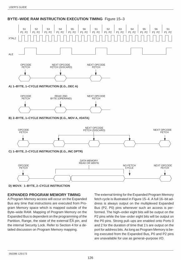
USER’S GUIDE
050396 125/173
126
BYTE–WIDE RAM INSTRUCTION EXECUTION TIMING Figure 15–3
S1P1 P2
S2P1 P2
S3P1 P2
S4P1 P2
S5P1 P2
S6P1 P2
S1P1 P2
S2P1 P2
S3P1 P2
S4P1 P2
S5P1 P2
S6P1 P2
S1P1 P2
OPCODEFETCH
NEXT OPCODEFETCH (DISCARD)
NEXT OPCODEFETCH
OPCODEFETCH
READ 2NDBYTE (OPERAND)
NEXT OPCODEFETCH
OPCODEFETCH
NEXT OPCODEFETCH (DISCARD) NEXT OPCODE
FETCH
OPCODEFETCH
NO FETCHCYCLE
NEXT OPCODEFETCH
DATA MEMORYREAD OR WRITE
XTAL2
ALE
A) 1–BYTE, 1–CYCLE INSTRUCTION (E.G., DEC A)
B) 2–BYTE, 1–CYCLE INSTRUCTION (E.G., MOV A, #DATA)
C) 1–BYTE, 2–CYCLE INSTRUCTION (E.G., INC DPTR)
D) MOVX: 1–BYTE, 2–CYCLE INSTRUCTION
EXPANDED PROGRAM MEMORY TIMINGA Program Memory access will occur on the ExpandedBus any time that instructions are executed from Pro-gram Memory space which is mapped outside of theByte–wide RAM. Mapping of Program Memory on theExpanded Bus is dependent on the programming of thePartition, Range, the state of the external EA pin, andthe internal Security Lock. Refer to Section 4 for a de-tailed discussion on Program Memory mapping.
The external timing for the Expanded Program Memoryfetch cycle is illustrated in Figure 15–4. A full 16–bit ad-dress is always output on the multiplexed ExpandedBus (P2, P0) pins whenever such an access is per-formed. The high–order eight bits will be output on theP2 pins while the low–order eight bits will be output onthe P0 pins. Strong pull–ups are enabled onto Ports 0and 2 for the duration of time that 1’s are output on theport for address bits. As long as Program Memory is be-ing executed from the Expanded Bus, P0 and P2 pinsare unavailable for use as general–purpose I/O.

USER’S GUIDE
050396 126/173
127
Multiplexed address and data information appear on thePort 0 pins as Program Memory fetches are performedon the Expanded Bus. The falling edge of ALE can beused to signal when the lowest eight bits of valid ad-dress information are being output on Port 0 when sucha fetch occurs. In addition, ALE is activated twice everymachine cycle during access to Program Memory, re-gardless of whether the fetch takes place to RAM or tothe Expanded Bus. Whenever a Program Memory fetchtakes place on the Expanded Bus, the SFR latch for Port0 is written with all 1’s (0FFH) so that the original in-formation contained in this register is lost. Port 0 pinsare driven with internal buffers when 1’s are output dur-ing Expanded Program Memory cycles.
The PSEN signal is provided as the read strobe pulsefor Expanded Program Memory fetches. When theSecure Microcontroller is accessing Program Memoryfrom Byte–wide RAM, PSEN will remain inactive. Dur-ing Program Memory fetches on the Expanded Bus, it isactivated twice every machine cycle, except when aMOVX instruction is being executed. As discussed inthe previous section, not all bytes fetched from Expand-ed Program Memory are actually used by the CPU dur-ing instruction execution. A complete memory cycle, in-cluding the enabled and disabling of both ALE andPSEN, takes six clock oscillator periods. This is one–half of a machine cycle.
EXPANDED PROGRAM MEMORY FETCH Figure 15–4
MACHINE CYCLE MACHINE CYCLE
ALE
PORT 0
PORT 2
PCLOUT
PCLOUT
PCLOUT
PCLOUT
PCH OUT
DATASAMPLED
DATASAMPLED
DATASAMPLED
DATASAMPLED
PSEN
PCH OUT PCH OUT PCH OUT PCH OUT
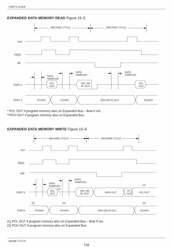
USER’S GUIDE
050396 127/173
128
EXPANDED DATA MEMORY READ Figure 15–5
PSEN
MACHINE CYCLE MACHINE CYCLE
ALE
PORT 0
PORT 2 PCH/P2 PCH/P2 DPH OR P2 OUT PCH/P2
PCLOUT
DPL ORRI, OUT
PCLOUT
DATASAMPLED
DATASAMPLED
DATASAMPLED
RD
* PCL OUT if program memory also on Expanded Bus – float if not.**PCH OUT if program memory also on Expanded Bus.
EXPANDED DATA MEMORY WRITE Figure 15–6
PSEN
MACHINE CYCLE MACHINE CYCLE
DATASAMPLED
DATASAMPLED
ALE
PORT 0
PORT2 PCH/P2 PCH/P2 DPH OR P2 OUT PCH/P2
PCLOUT PCL OUT
PCOUT
DPL ORRI, OUT DATA OUT
(1)
(1)
(2) (2) (2)
WR
(1) PCL OUT if program memory also on Expanded Bus – float if not.(2) PCH OUT if program memory also on Expanded Bus.
USER’S GUIDE
050396 128/173
129
EXPANDED DATA MEMORY TIMINGThe timing for the Expanded Data Memory access cycleis illustrated in Figures 15–5 and 6. Accesses to DataMemory on the Expanded Bus will occur any time that aMOVX instruction is executed that references a DataMemory location that is mapped outside the area whichhas been assigned to the Expanded Bus via the Parti-tion and Range.
When a MOVX instruction is used with the Data Pointerregister (e.g., MOVX @DPTR) to access a DataMemory location on the Expanded Bus, a full 16–bit ad-dress will be generated to the external memory. The16–bit address is generated on P2 and P0 which are thesame pins as for a Program Memory fetch from Expand-ed Memory. The contents of the SFR latch for Port 2 willnot be modified, however, during the execution of a DataMemory fetch cycle on the Expanded Bus. If the MOVXinstruction is not followed by another instruction requir-ing a cycle on the Expanded Bus, then the original con-tents of the Port 2 SFR latch will appear once again dur-ing the next machine cycle.
Multiplexed address/data information is output on Port 0during the execution of a Data Memory cycle on the Ex-panded Bus. The falling edge of ALE can be used tolatch the lower eight bits of address information into anexternal transparent latch (e.g., 74LS373 or equiva-
lent). During the second cycle of a MOVX instruction,the first ALE pulse will not be generated so that valid ad-dress information will remain in the latch and be pres-ented to the external memory device for the duration ofthe cycle. Port 0 is written with all 1’s (0FFH) so that theoriginal information contained in this register is lost.Also, Port 0 pins are driven with internal buffers when 1’sare output during Expanded Data Memory cycles.
When a MOVX instruction is used with an indirect regis-ter address (e.g., MOVX @R0) for the same purpose,only an 8–bit address will be generated for the currentinstruction. This 8–bit address will appear on Port 0,while the contents of the SFR latch for Port 2 will remainon Port 2.
When data is to be read from Data Memory on the Ex-panded Bus, the external RD pin will be activated duringthe second machine cycle of the MOVX instruction. Acomplete RD cycle, including activation of ALE and RD,takes twelve clock oscillator periods. PSEN is inactiveduring this machine cycle. This cycle is illustrated in Fig-ure 15–5. When the MOVX instruction specifies a writeoperation to the external memory device, the WR signalwill be activated as shown in Figure 15–6. Data is outputon Port 0 just before WR is activated and remains validuntil it goes back to its inactive level at the conclusion ofthe cycle.

USER’S GUIDE
050396 129/173
130
SECTION 16: PROGRAM LOADING
INTRODUCTIONProgram loading is performed to initialize the contentsof NV RAM and to configure the microcontroller. Load-ing is done using a Bootstrap ROM Loader built into allmembers of the Secure Microcontroller family. Whenthis Bootstrap Loader is invoked, the user’s NV RAMappears as data memory to the ROM and can thereforebe initialized. Once loading is complete, the BootstrapROM then becomes transparent. It has no effect on theuser’s memory map and is completely invisible. Boot-strap Loading is normally done for the initial programloading. There are no restrictions on using it forupgrades or reprogramming, though it is possible usingthe memory mapping features, to perform partialreloads without invoking the loader.
The Bootstrap Loader is primarily used to initializememory, but it is capable of several other functions. Itcan change the memory map configuration, dump orverify the contents of memory, perform a CRC check, filla block with a constant, manipulate the security featuresand the I/O ports. It can not display or edit the Scratch-pad RAM (128 bytes) or SFRs since it uses theseresources for its own operation. Note that the Scratch-pad RAM will be erased by the loader. Therefore theloader should not be invoked while critical data is storedin this area. The MOVX RAM area will not be altered bythe loader unless a user requests that this be done.
Each version of microcontroller has different loadermodes and different commands. All versions are capa-ble of being programmed via the serial port and this isthe preferred method. The DS5000 series is also capa-ble of a parallel programming technique similar to anEPROM–based 8051. The DS5001/DS5002 seriessupports an alternate parallel load mode that is for useby a host microprocessor using the 8042–type RPCmode. The following discussions explain the methods ofinvoking the Bootstrap Loader. Then the different pro-gramming modes are described. The remaining sec-tions give a detailed description of the commands andsyntax used by the Bootstrap ROM.
The DS5000 series [DS5000(T), DS2250T, andDS5000FP] and the DS5001/2 series [DS5001FP,DS2251T, DS5002FP, DS2251T] have different pro-gram loading modes available. The DS5000 series canbe loaded via its serial port or in a parallel fashion like anEPROM type 87C51. The serial mode allows theDS5000 to be programmed in a fixture or while installed
in the end system. The parallel method requires asuper–voltage and is normally done in a fixture only. TheDS5001 series has a similar serial mode with the samebenefits. The parallel mode is entirely different. TheDS5001FP or DS5002FP, using its RPC slave interface,can be loaded in a parallel manner by a host micropro-cessor. This is also an in–system technique but could beperformed in a fixture. It requires no super–voltagepulses. Note that this mode is a high–speed loader andbears no resemblance to an 87C51 load mode.
Note: Dallas Semiconductor highly recommendsthat serial load capability be designed into the tar-get system . This provides substantial flexibility toupgrade and troubleshoot the system. Using in–systemserial loading allows a product to take full advantage ofthe Secure Microcontroller’s features.
INVOKING THE BOOTSTRAP LOADERThe Secure Microcontroller defaults to normal operating(non–loader) mode without external hardware. If theloader mode is desired, it can be invoked at any timeusing the methods described later in this section. Oncethe Bootstrap Loader session is complete, the devicewill perform a hardware reset and begin operation. Thiswill be identical to an external reset, except that thebootstrap loader, as part of normal operation, will modifyvarious locations in scratchpad RAM. The followingtable shows which areas of scratchpad RAM are guar-anteed destroyed, guaranteed preserved, or will be ofindeterminate state after exiting the bootstrap loader.
DS5000FP DS5001/2FP
Guaranteed Preserved None 70h–7Fh
Indeterminate None 38h–6Fh
Guaranteed Destroyed 00h–7Fh 0h–37h
The guaranteed preserved locations are areas inscratchpad RAM that will not be changed by the boot-strap loader. These locations as useful for storing datasuch as serial numbers, which should be retainedregardless of the software. Similarly, the guaranteeddestroyed locations have all been overwritten duringbootstrap loader execution with indeterminate data.These locations can be used to store security–sensitivedata, because it will be erased by the loader beforeanother program can read it out.
USER’S GUIDE
050396 130/173
131
The indeterminate area contains various stacks andbuffers used by the loader, and a given byte in this areamay or may not be modified by the loader. As such theuser should not rely on the bootstrap loader preservingany data in this area. In a like manner, because not alllocations are used, the indeterminate area of scratch-pad RAM should not be used for storing security–sensi-tive data.
The methods of invoking the loader vary between theDS5000 series and DS5001/DS5002 series, and aredescribed below.
DS5000 SeriesThe DS5000 is placed in its Program Load configurationby simultaneously applying a logic 1 to the RST pin andforcing the PSEN line to a logic 0 level. Immediately fol-lowing this action, the DS5000 will look for a serial ASCIIcarriage return (0DH) character received at 57600,19200, 9600, 2400, 1200, or 300 bps over the serial portor a Parallel Program Load pulse. For whichever type isfirst detected, the DS5000 will place itself in theassociated Program Load mode. If an ASCII <CR>character is detected first, then the DS5000 will place it-self in the Serial Program Load mode and will ignore anyParallel Program Strobe pulses. Conversely, if a Paral-lel Program Strobe pulse is first detected, then theDS5000 will be placed in the Parallel Program Loadmode and all incoming data on the serial port will be ig-nored. The selected program load mode will remain ineffect until the next time power is removed from the de-vice or when the Program Load configuration (RST=1,PSEN=0) is removed.
In normal programming of the DS5000, problems withselection of the incorrect Program Load mode will not beencountered. When the DS5000 is placed in an8751–compatible programming system, no serial datawill be applied on the RXD pin for the serial port. As aresult, there is almost no chance of random activity onthis pin being interpreted as a <CR> character at a validbaud rate. Similarly, serial program loading will mostoften be performed in the end system. Consequently,there is again almost no chance of a valid Parallel Pro-gram Strobe pulse (with VPP voltage at 13V) being inter-preted as a signal to invoke the Parallel Program Loadmode when the Serial Program Load mode is desired.
If the Program Load configuration is removed such thatRST=0 and PSEN=1 with power still applied at VCC, the
device will undergo an internal hardware reset and willbegin executing code from the reset vector at 0000h inProgram Memory.
DS5001/DS5002 SeriesThe DS5001 and DS5002 microcontrollers use an iden-tical method to invoke the bootstrap loader. A fallingedge on the PROG pin will invoke the loader with asingle device pin. Note that the PROG pin must remainlow for 48 oscillator clocks to be certain of recognition.Taking the PROG pin to a logic 1 will remove the loaderand cause the DS5001 to perform a reset. Note also thatthe PROG pin must be high for as much as 48 clocksbefore the CPU is guaranteed to exit the loader. Thisconstitutes the “pseudo–edge” detection of the programpin. Note also that pulling RST=1 and PSEN=0 will alsocause the loader to be invoked.
Once the loader mode stimulus has been detected, theDS5001 will begin looking for an ASCII carriage return(0Dh). It will look at the serial port and the RPC (8042)port. For serial reception, the loader will auto–baud at57600, 19200, 9600, 2400, 1200 and 300 bps. For RPCmode, the 0Dh value must be written into the Data Inbuffer as described in the RPC section under ParallelI/O. When either of these conditions is detected, theloader will place itself in that loader mode. Activity onthe other port will be ignored. This condition will remainuntil the loader is exited or power is cycled. When theloader stimulus is removed, the processor will perform ahardware reset and begin execution at location 0000h.
EXITING THE LOADERThe normal method of leaving the loader is to removethe stimulus that invoked it. In the DS5000 series, theRST pin, must be driven low or allowed to float and thePSEN signal should be allowed to float. The RST pinhas an internal pull–down. The PSEN is an output andwill drive itself. Note that both of these conditions mustoccur or the loader will not be exited. For the DS5001,there are several options. If the RST and PSEN option isused, the they must be removed as described above. IfPROG is pulled low, it can either be returned high or theExit “E” command can be issued. Since the loader isedge activated, this will restart the user’s code evenwhile the PROG pin is low. If power were to cycle whilethe PROG pin were low, the loader would be invoked onpower up. The flow of these conditions is shown inFigure 16–1.
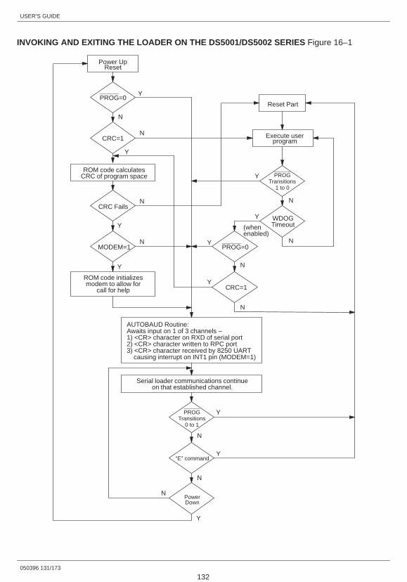
USER’S GUIDE
050396 131/173
132
INVOKING AND EXITING THE LOADER ON THE DS5001/DS5002 SERIES Figure 16–1
AUTOBAUD Routine:Awaits input on 1 of 3 channels –1) <CR> character on RXD of serial port2) <CR> character written to RPC port3) <CR> character received by 8250 UART causing interrupt on INT1 pin (MODEM=1)
Power UpReset
CRC=1
PROG=0
ROM code calculates
CRC Fails
MODEM=1
ROM code initializes
CRC of program space
modem to allow forcall for help
Serial loader communications continueon that established channel.
PROGTransitions
0 to 1
“E” command
PowerDown
PROG=0
CRC=1
(whenenabled)
WDOGTimeout
PROGTransitions
1 to 0
Reset Part
Execute userprogram
Y
N
N
Y
N
N
Y
Y
N
N
Y
Y
Y
N
N
N
Y
Y
Y
Y
N
N
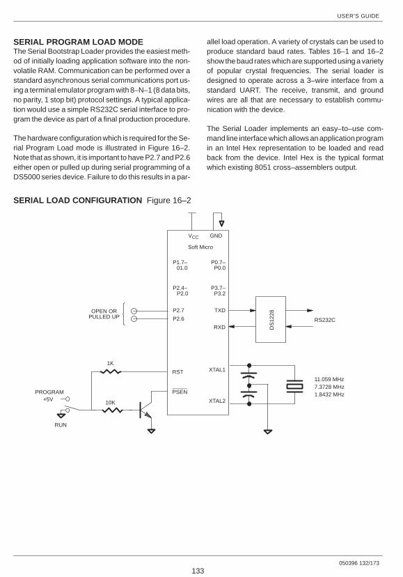
USER’S GUIDE
050396 132/173
133
SERIAL PROGRAM LOAD MODEThe Serial Bootstrap Loader provides the easiest meth-od of initially loading application software into the non-volatile RAM. Communication can be performed over astandard asynchronous serial communications port us-ing a terminal emulator program with 8–N–1 (8 data bits,no parity, 1 stop bit) protocol settings. A typical applica-tion would use a simple RS232C serial interface to pro-gram the device as part of a final production procedure.
The hardware configuration which is required for the Se-rial Program Load mode is illustrated in Figure 16–2.Note that as shown, it is important to have P2.7 and P2.6either open or pulled up during serial programming of aDS5000 series device. Failure to do this results in a par-
allel load operation. A variety of crystals can be used toproduce standard baud rates. Tables 16–1 and 16–2show the baud rates which are supported using a varietyof popular crystal frequencies. The serial loader isdesigned to operate across a 3–wire interface from astandard UART. The receive, transmit, and groundwires are all that are necessary to establish commu-nication with the device.
The Serial Loader implements an easy–to–use com-mand line interface which allows an application programin an Intel Hex representation to be loaded and readback from the device. Intel Hex is the typical formatwhich existing 8051 cross–assemblers output.
SERIAL LOAD CONFIGURATION Figure 16–2
PSEN
RST
+5V
1K
10K
RS232C
11.059 MHz7.3728 MHz1.8432 MHz
DS
1228
VCC GND
Soft Micro
P2.7
P2.6
TXD
RXD
XTAL1
XTAL2
P1.7–
P2.4–
01.0
P2.0
P0.7– P0.0
P3.7–P3.2
PROGRAM
RUN
OPEN ORPULLED UP

USER’S GUIDE
050396 133/173
134
AUTO–BAUD RATE DETECTIONThe Serial Bootstrap Loader has the capability of deter-mining which of the six supported baud rate frequenciesis being used for communication and initializing its inter-nal hardware for communication at that frequency.When the Program Load mode is first invoked, the de-vice will watch for activity on the serial port. If a <CR>character is received at one of the six supported baudrates, then operation in the Serial Program Load modewill be established. The loader expects to talk asynchro-nously at 300, 1200, 2400, 9600, 19200, or 57600 baud
using eight data bits, no parity, and one stop bit in full du-plex. A break signal followed by a carriage return willcause a re–determination of baud rate. Although an11.0592 MHz crystal is standard for generating baudrates, the auto–baud rate detector allows a variety ofcrystals to be used. If a crystal frequency other than11.0592 MHz is used, then the baud rate frequencieswhich will be recognized by the serial loader are shownin Table 16–1. Other crystals will generate non–stan-dard band rates.
SERIAL LOADER BAUD RATES FOR DIFFERENT CRYSTAL FREQUENCIES Table 16–1
BAUD RATE
CRYSTAL FREQ (MHz) 300 1200 2400 9600 19200 57600
14.7456 Y Y Y Y
11.0592 Y Y Y Y Y Y
9.21600 Y Y Y Y
7.37280 Y Y Y Y
5.52960 Y Y Y Y
1.84320 Y Y Y Y
USER’S GUIDE
050396 134/173
135
BOOTSTRAP LOADER INITIALIZATIONWhen loader mode is invoked, the device will await anincoming <CR> character at a valid baud rate througheither the serial port (in Serial Program Load mode) orvia the parallel interface (in Parallel Program Loadmode). At this point, the bootstrap loader will transmit a
banner to the host to indicate that it has been invoked.The banner will appear similar to the one shown below,but will vary between specific members of the SecureMicrocontroller family and between revision levels. Thebanner will be followed by a “>” prompt which indicatesthe device is ready to receive a command.
DS500X LOADER VERSION X.X COPYRIGHT (C) XXX DALLAS SEMICONDUCTOR>
COMMAND LINE INTERFACEThe Secure Microcontroller family implements an easy-to–use command line interface which is very similar tothose found in debugging environments. The Serial
Bootstrap Loader responds to single character alpha-betic commands which are summarized below. Thereare differences between versions as noted. A detaileddescription of each command follows.
COMMAND FUNCTION VERSION
C CRC–16 of RAM AllD Dump Intel hex file AllE Exit loader DS5001FP/DS5002FPF Fill RAM with a constant AllG Get value from ports AllI Include CRC DS5001FP/DS2251TK Load 40–bit key DS5000FP/DS2250T/DS5000(T)L Load Intel Hex file AllN New – invoke Freshness DS5001 seriesP Put a value to the ports All (DS5000 after Rev. D4)R Read configuration AllT Trace (echo) incoming data AllU Unlock security AllV Verify RAM against incoming Hex AllW Write register(s) AllZ Lock All^C Reset loader AllXon/Xoff Flow control of serial transmission All
Selected commands require arguments and some com-mands have optional arguments. In all cases, argu-ments are expected to be hexadecimal numbers. Inaddition, an ASCII control–C character (^C) will causethe Serial Loader to terminate any function currently be-ing executed and display the command line prompt. Anincoming break character (defined as a received nullcharacter (00H) with the stop bit = 0) will cause the Seri-al Bootstrap Loader to be restarted and the baud rate re-determined.
COMMAND LINE SYNTAXSingle–letter ASCII characters are recognized as com-mands. Arguments are represented by hexadecimal
numbers. A hexadecimal number is any sequence ofhexadecimal characters. A hexadecimal character maybe a digit, 0 through 9, or one of the letters A through F. Abyte will always be the right–most two digits of a hexa-decimal number. For example, the following hexadeci-mal numbers will result in the following bytes:
A → 0AHAB → 0ABHABC → 0BCHABCD → 0CDH
USER’S GUIDE
050396 135/173
136
An address will always be the right–most four digits of ahexadecimal number. For example, the following hexa-decimal numbers will result in the following addresses:
A → 000AHAB → 00ABHABC → 0ABCHABCD → 0ABCDHABCDE → 0BCDEH
The D and F commands allow optional addresses to beentered. The syntax [Begin–Address [End–Address]] isused to convey the following meanings:
a) No arguments: Begin–Address is set to 0 and End-Address is set to the Range.
b) One argument: Begin–Address is set to the argu-ment and End–Address is set to the Range.
c) Two arguments: Begin–Address is set to the first ar-gument and End–Address is set to the second argu-ment. This second address may exceed the addressvalue specified by the Range.
In cases b and c, the End Address may not be less thanthe Begin Address, either implicitly or explicitly. RAM willbe addressed from 0 to 1FFF for 8K RAM and from 0 to7FFF for 32K RAM. This maximum value is determinedby the Range.
Error messages will be printed as soon as errors are de-tected. All messages are preceded by the two charac-ters ‘E:’, and followed by a mnemonic description.
Commands will not be processed until an entire com-mand line is entered and terminated with a <CR>. Nocommand line may be greater than 16 bytes, which isthe maximum number of characters in the K command.Since a command line is not processed until a <CR> isentered, it may be edited with the delete key which willdo a destructive delete to the screen. Lines longer than16 characters will cause an error message to be dis-played and no action to be taken on the command line.
Only legal characters will be echoed back to the screen.The legal characters are: 0123456789 <:>, <space>,ABCDEFGHIJKLMNOPQRSTUVWXYZ, and <de-lete>. Backspace characters (<BS>) are converted todelete characters. The horizontal tab character is con-
verted to space. Lower case alphabetic characters areconverted to upper case alphabetic.
The <delete> character is executed as a <BS> <space><BS> when possible in command mode. This will causethe character to be overprinted on a hardcopy device.The <CR> character generates a <CR> <LF> pair.
The Serial Bootstrap Loader will respond to XOFF char-acters by stopping transmission as soon as the charac-ter is received. A control–C or an XON will resume serialtransmission. The Serial Bootstrap Loader will nottransmit a XOFF character. The program is able to keepup with input as long as the receiver can keep up with itsoutput. The receiver should be programmed to quittransmission after it sends an XOFF and transmit any-thing before sending an XON.
Intel Hex data is not echoed unless the Trace mode istoggled on.
COMMAND SUMMARIES^CInterrupt whatever is going on, clear all the buffers, putup a prompt and wait for the next command. Anything inthe type–ahead buffer is removed. All output is stopped.If trace had been on before, it is cleared. If XOFF hadbeen in effect, it is cleared.
C [begin–address [end–address]]Return the CRC–16 (cyclic redundancy check) of theNV RAM. This computation is performed over theRange unless optional start and end addresses are giv-en. The CRC–16 algorithm is commonly used in datacommunications.
D [begin–address [end–address]]Dump memory in Intel Hex Format. An optional addressrange may be specified. Each record will contain up to32 data bytes. The last line printed is the end–of–datarecord.
EThe serial loader is exited. This works if a negative edgeon PROG was used to invoke it, or a CRC check failed.

USER’S GUIDE
050396 136/173
137
F byte [begin–address [end–address]]Fill memory with the value of the specified byte. An op-tional address range may be specified.
GData is read from ports 0, 1, 2 and 3 and is printed as fourpairs of hexadecimal digits.
IA CRC–16 is computed from 0 to CRC_RANGE minus 2and the computed CRC is put into CRC_RANGE minusone and CRC_RANGE. This is used when power–onCRC checking is desired. This command will printDONE when it finishes.
K byte–1 byte–2 byte–3 byte–4 byte–5Load the encryption key word. The five bytes areechoed before they are put into the registers.
LLoad standard Intel Hex formatted data into memory.Only record types 00 and 01 are processed. Each line ofthe file is treated the same way. All characters are dis-carded before the header character ‘:’ is read. The restof the record, defined by the length byte, is then pro-cessed. Control returns to the command prompt after anIntel End Record is encountered. Each byte put tomemory, is read back to verify it is there. If the byte readback is different, an error is reported. All errors are re-ported immediately after the character is received whichcaused the error. The program will then read charactersuntil a colon is found and then attempt to process thedata input from the command line. Note that all bytes areput to memory as they are encountered. This meansthat if a bad checksum is found, an error will be reported,but all the bytes on the line will have been put to memory.
MToggle the status of the modem available bit (MDM inthe CRC register). This will display either AVAILABLEor UNAVAILABLE. This command is only available withthe DS5001FP or DS2251T.
NThe Newness command, N, will place the device intofreshness mode if VCC is removed following executionof the command. After typing “N” the device will promptCONFIRM:. At this point the host system must replyFRESH, followed by a carriage return, to complete theprocess. If completed successfully, the message
POWER DOWN TO MAINTAIN FRESHNESS will bereturned. Deviation from this sequence will display themessage DID NOT CONFIRM and return to the loaderprompt. This command is only available with theDS5001FP, DS5002FP or modules based on theseparts. This command may not be executed when talkingthrough the modem to the serial loader.
PDS5000:P <P0 value> <P1 value> <P2 value> <P3 value>Writes values to all ports simultaneously. DS5001/DS5002:P <port> <value>Writes value to the requested port.
RDS5000:Displays the value of the MCON register.DS5001/DS5002:Displays the values of the MCON register, RPCTL reg-ister, MSL bit, and CRC registers in the following form:MCON:XX RPCTL:XX MSL:XX CRC:XX.The CALIB register is no longer supported and shouldbe ignored. CRC is not displayed on DS5002.
TTrace by echoing the incoming Intel Hex data. This is atoggle command and will display the state after toggling.Initially the state of the toggle is OFF.
UClear the Security Lock. The Range is set to 32K and thepartitioning is set to all program memory. Note that un-locking the Security Lock clears the encryption regis-ters, Vector RAM, and selects CE1 for the RAM. The Uand Z commands are the only commands that may beexecuted when the chip is locked.
VVerify current contents of memory with the Intel Hexcoming in. This command operates similar to the Loadcommand, except that it does not write to RAM; it simplycompares the byte in memory to the byte in the datastream. A message is reported if an error is detected.
W byteDS5000:Writes byte to the MCON register to configure the Parti-tion, Range, and ECE2 bits. The PAA and SL bits are
USER’S GUIDE
050396 137/173
138
unaffected by this command.DS5001/DS5002:W [CRC/MCON/MSL/RPCTL] byteWrites byte to the requested register. The SL bit is unaf-fected by this command. This command is discussed ingreater detail later in this section.
ZSet the Security Lock. Only the U and Z commands maybe given after the Security Lock is set.
^CRestarts most operations. N cannot be restarted.
Xon/XoffThese two characters provide flow control to the serialloader. The serial loader will never issue them, but willrespond to both. Xoff (control–S, DS3, 0x13) requeststhat character transmission stop. Xon (control–Q, DC1,0x11) requests the resumption of transmission.
NOTES ON SELECTED DS5001FP ANDDS5002FP COMMANDSWhen using the Include command ‘I’, certain precau-tions are needed, The CRCBIT (bit 0) of the CRC SFR(C1h) must be set or the error message E:NOCRCB isprinted. The MSL bit must not be cleared (via loader) orthe error message E:NOTCOD is printed. If the PM bit(bit 1) of the MCON SFR (C6h) is one, thenCRC_RANGE must be less than or equal to the pro-gram Range, or else the error message E:BADRNG isprinted.
When storing an end system, it may not be desirable tolithium–back RAM or a real–time clock. The Newnesscommand ‘N’ will accomplish this. When ‘N’ is issued,the loader will prompt with CONFIRM: after the N isentered. The user must type FRESH without anyspaces or deletes and terminate it with a carriage returnto put the part into freshness. The message DID NOTCONFIRM is printed if a mistake is made while enteringFRESH; otherwise the message POWER DOWN TOMAINTAIN FRESHNESS is printed. The ‘N’ commandshould be the last function that is executed. After this,the system should be powered down for storage. At thistime, the VCCO will be pulled low, removing power fromRAM or clock. The newness command may not beexecuted when talking through the modem to the serialloader. If it is attempted, the error message E:ILLCMDis printed.
The DS5001FP and DS5002FP provide loader com-mands to assist in system checkout. These are ‘G” Getand ‘P’ Put. Get will read the values of all four I/O ports.Put is used to write a value to a port. This allows a mea-sure of hardware control while the device is effectively ina reset state. If a port number other than 0, 1, 2, or 3 isused, the error message E:BADREG is printed. Ports 0and 2 may not be altered when talking to the loaderthrough the RPC interface. The error messageE:BADREG is printed if it is attempted. Bits 0 and 1 ofport 3 will always be written as ones when port 3 isaltered (serial port).
The DS5001FP/DS5002FP write command has moreoptions than the DS5000 version. Any of the followingregisters/functions can be initialized using the loader.VAL is written to the requested register. If an illegal reg-ister name is entered, the error message E:BADREG isprinted.
CRC This register selects the range overwhich a power–on CRC will be per-formed, and enables the process. Onlybits 0, 4, 5, 6 and 7 of the CRC registermay be altered. Bits 1, 2, and 3 are leftalone.
MCON Controls range, partition, and peripheralselects, All but bit 0 of the MCON regis-ter may be altered.
MSL This bit allows the data space in a fixedmemory (non–partitionable) system tobe loaded using the loader software.MSL only uses the low order bit of valueto change the MSL bit. In fixed partitionand 128K mode, if MSL equals 0, pro-gram loads/verifies will go to data space.Upon entry, MSL will be = 1. MSL has noeffect in user mode.
RPCTL RPCTL only uses the low order bit of VALto change bit 0 of the RPCTL register.The LSB of the RPCTL is also used todetermine the Range.
Only record types 00 (data) and 01 (end) may beloaded. Other record types will cause the error mes-sage E:BADREC to be printed out, but loading will con-tinue with the next valid record. The last two bytes ofeach record contain a checksum. This checksum is
USER’S GUIDE
050396 138/173
139
compared to the computed value for the record, and ifdifferent, the error message E:BADCKS is printed out.Unfortunately, the data bytes for this record will havebeen put to memory already. End of Data records (01)do not check for valid checksums. After a byte is put tomemory, it is read back immediately to see if it is thesame. If not, the error message E:MEMVER is printed.
ERROR MESSAGESE:ARGREQAn argument or arguments is required for this com-mand.
E:BADCKSThe checksum found at the end of an Intel Hex recordloaded into RAM is not the same as the same as thevalue calculated. The last 2 bytes of each record con-tain a checksum. End of data records (01) do not checkfor valid checksums.
E:BADCMDAn invalid command letter was entered.
E:BADRECA record type other than 00 (data) or 01 (end) wasencountered while reading an Intel Hex data record.Loading will continue with the next valid record.
E:BADREGA port number other than 0, 1, 2, or 3 was used as anargument for a P command. This message is alsoprinted if register other than CALIB, CRC, MCON, MSL,or RPCTL was used as an argument for a W command.
E:BADRNGThe CRC_RANGE must be less than or equal to theProgram Range if the PM bit is set. The CRC_RANGEmust be less than or equal to the Program Range andthe partition if the PM bit is cleared.
E:EXTARGExtra data was encountered on the command line whenit wasn’t needed. Reenter the command.
E:ILLCMDAn illegal command was entered via the modem. Reen-ter the command.
E:ILLOPTThe optional parameters given were in error. If the startaddress is greater than the given address, either implic-itly or explicitly, then an error is printed. The range bit im-plicitly determines the maximum range.
E:LOCKEDThe requested operation cannot be performed becausethe device is locked.
E:MEMVERAn error was encountered while programming or verify-ing a byte in RAM. Reload the record or file. Repeatederror messages may indicate a bad device.
E:NOCRCBThe CRC bit (bit 0) of the CRC SFR must be set whenusing the Include command. The Include command isnot supported on the DS5002FP/DS2252T.
E:NOTCODThe Include command was entered while the MSL bitwas cleared. The MSL bit must be set (via loader) whenusing the Include command.
E:NOTHEXA non–hexadecimal character was found whenexpected.
E:VERIFYThe byte which was sent did not verify with the corre-sponding one in RAM.
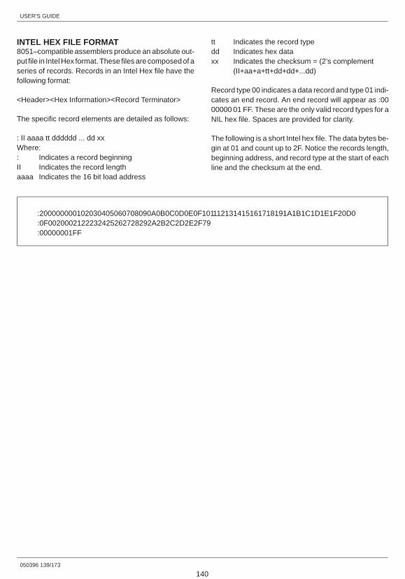
USER’S GUIDE
050396 139/173
140
INTEL HEX FILE FORMAT8051–compatible assemblers produce an absolute out-put file in Intel Hex format. These files are composed of aseries of records. Records in an Intel Hex file have thefollowing format:
<Header><Hex Information><Record Terminator>
The specific record elements are detailed as follows:
: II aaaa tt dddddd ... dd xxWhere:: Indicates a record beginningII Indicates the record lengthaaaa Indicates the 16 bit load address
tt Indicates the record typedd Indicates hex dataxx Indicates the checksum = (2’s complement
(II+aa+a+tt+dd+dd+...dd)
Record type 00 indicates a data record and type 01 indi-cates an end record. An end record will appear as :0000000 01 FF. These are the only valid record types for aNIL hex file. Spaces are provided for clarity.
The following is a short Intel hex file. The data bytes be-gin at 01 and count up to 2F. Notice the records length,beginning address, and record type at the start of eachline and the checksum at the end.
:200000000102030405060708090A0B0C0D0E0F101112131415161718191A1B1C1D1E1F20D0:0F0020002122232425262728292A2B2C2D2E2F79:00000001FF
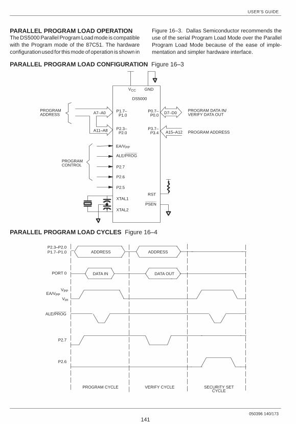
USER’S GUIDE
050396 140/173
141
PARALLEL PROGRAM LOAD OPERATIONThe DS5000 Parallel Program Load mode is compatiblewith the Program mode of the 87C51. The hardwareconfiguration used for this mode of operation is shown in
Figure 16–3. Dallas Semiconductor recommends theuse of the serial Program Load Mode over the ParallelProgram Load Mode because of the ease of imple-mentation and simpler hardware interface.
PARALLEL PROGRAM LOAD CONFIGURATION Figure 16–3
ALE/PROG
PSEN
RST
D7–D0
A15–A12 PROGRAM ADDRESS
PROGRAM DATA IN/VERIFY DATA OUTA7–A0
A11–A8
PROGRAMADDRESS
PROGRAMCONTROL
VCC GND
DS5000
P1.7– P1.0
P2.3– P2.0
EA/VPP
P2.7
P2.6
P2.5
XTAL1
XTAL2
P0.7–P0.0
P3.7–P3.4
PARALLEL PROGRAM LOAD CYCLES Figure 16–4
ALE/PROG
ADDRESS
DATA IN
ADDRESS
DATA OUT
PROGRAM CYCLE VERIFY CYCLE SECURITY SETCYCLE
P2.3–P2.0P1.7–P1.0
PORT 0
EA/VPP
P2.7
P2.6
VPP
VIH

USER’S GUIDE
050396 141/173
142
PARALLEL PROGRAM LOAD MODETable 16–3 summarizes the selection of the availableParallel Program Load cycles. Figure 16–4 illustratesthe timing associated with these cycles.
8751–COMPATIBLE PROGRAM LOAD CYCLES Table 16–3
MODE RST PSEN PROG EA P2.7 P2.6 P2.5
Program 1 0 0 VPP 1 0 X
Security Set 1 0 0 VPP 1 1 X
Verify 1 X X 1 0 0 X
Prog Expanded 1 0 0 VPP 0 1 0
Verify Expanded 1 0 1 1 0 1 0
Prog MCON or Key 1 0 0 VPP 0 1 1
Verify MCON 1 0 1 1 0 1 1
The Program cycle is used to load a byte of data into aregister or memory location within the DS5000. TheVerify cycle is used to read this byte back for compari-son with the originally loaded value to verify proper load-ing. The Security Set cycle may be used to enable theSoftware Security feature of the DS5000. One may alsoenter bytes for the MCON register or the Encryption Keyusing the Program MCON cycle. When using this cycle,the absolute register address must be presented at Port1 and 2 as is the normal Program cycle (Port 2 should be00H). The MCON contents can be likewise verified us-ing the Verify MCON cycle.
When the DS5000 first detects a Parallel ProgramStrobe pulse or a Security Set Strobe pulse while in theProgram Load mode following a Power–On Reset, theinternal hardware of the DS5000 is initialized so that anexisting 4K byte 8751 program can be programmed intoa DS5000 with little or no modification. This initializationautomatically sets the Range Address for 8K bytes andmaps the lower 4K byte bank of Embedded RAM as Pro-gram Memory. The top 4K bytes of Embedded RAM aremapped as Data Memory. In order to program code (andthereby use the DS5000–enhanced capability), the Pro-gram/Verify Expanded cycles can be used. Up to32K bytes of program code can be entered and verified.Note that the expanded 32K byte Program/Verify cyclestake much longer than the standard cycles.
A typical parallel loading session would follow this pro-cedure. First, set the contents of the MCON register withthe correct range and partition (if using expanded pro-gramming). Next, the Encryption Key can be loaded ifdesired. Then, program the DS5000 using either stan-dard or expanded program cycles and verify. Last, turnon the security lock using a Security Set cycle.
The Security Set strobe pulse from an 8751–compatibleprogramming system can be used to enable the Soft-ware Security feature of the DS5000. To explain this op-eration on the DS5000, it is useful to review how thisfunction works with the 8751. The Security Set Strobepulse is used to program the EPROM Security Lock biton an 8751. The programmed bit disables the on–chipEPROM memory from being read back during a Verifycycle. The bit can only be erased by UV light when therest of the program is erased.
With the DS5000, the Security Set Strobe pulse servesa similar function for its NV RAM–based Security Lockwhich when set disables the NV RAM from beginningread either through a Verify cycle in the Parallel Pro-gram mode or back through the serial port in the SerialPort mode. When a Security Set Strobe pulse is re-ceived by the DS5000, the current state of the SecurityLock bit is checked. If it is currently a 0, it will be set to 1.The Security Lock can be cleared by clearing the LSB ofthe MCON register.
USER’S GUIDE
050396 142/173
143
PARALLEL PROGRAMMING CONCERNSDallas Semiconductor highly recommends using theserial load mode for programming the DS5000. It hasproven highly reliable and easy to use. In the event thatparallel programming is still desirable to some users,several incompatibilities have been discovered in con-ventional device programmers. The following is a sum-mary of these incompatibilities:
1. The DS5000 is a fully CMOS device, and was actu-ally designed to be pin–compatible with the80C51/87C51 as opposed to the 8051/8751. As a re-sult there is a subtle difference between these twodevices. This has to do with the oscillator input pins,XTAL1 and XTAL2. On the CMOS devices, XTAL1is the pin which is driven in the external drive config-uration. On NMOS devices, XTAL2 is driven for theexternal clock configuration. This difference has noeffect when a crystal is tied to the pins for an externaltime base. However, many programming systemsuse the external drive configuration in order to main-tain the ability to program multiple types of devicesin a single 40–pin socket. For this reason, theDS5000 will not operate correctly in a 8751–compat-ible socket which uses the external clock mode.
2. The 87C51 data sheet specifies a “fast” program-ming timing algorithm for programming the locationsin its on–chip EPROM memory. This algorithm isidentical to the 8751 Program mode specificationexcept for the number and duration of ALE lowpulses during a “Program Byte” state. There are 25pulses specified, each with a low time of 90 to 110µs following by a minimum high time of 10 µs. Sincethe Parallel Load mode is partially implemented us-ing internal ROM firmware, the 87C51 fast program-ming algorithm is incompatible with the DS5000.Programming systems which implement this algo-rithm will not correctly program a DS5000.
3. Also since the Parallel Program mode is partiallyfirmware based, a minimum recovery time is re-quired between back–to–back Program Bytestrobes and between a Program Byte strobe fol-lowed by a Verify strobe.
4. Many programming systems apply VCC voltage dur-ing programming and remove it when programmingis completed. This operation is compatible with theDS5000 if the Power–On Reset time spec (tPOR) is
met before programming begins. Since there is nosimilar specification on the 8751 or on the 87C51,some programming systems may not meet theDS5000’s requirements and Program strobe pulsesmay not be recognized by the DS5000.
5. The DS5000 is compatible with either the 21V VPPof the 8751 or the 12V VPP of the 87C51. However,some programming systems sample the current thatis drawn during programming on the VCC pin and/oron the VPP pin. An 8751 is specified to draw a maxi-mum of 30 mA of IPP current during programming,while an 87C51 is specified for a maximum of 50 mA.A DS5000 will draw a maximum of only 15 mA of IPPcurrent during programming. As a result, these pro-gramming systems may erroneously report that thedevice is incorrectly installed in the socket.
Because of the limitations cited above, Dallas Semicon-ductor recommends that the Serial Bootstrap Loader beused for initial program loading of the DS5000.
RPC PROGRAM MODE OPERATIONThe DS5001FP and DS5002FP series offer high–speedprogramming mode with many of the benefits of theSerial Loader. Like the Serial mode, it is primarilyintended as an in–system technique but can be used ina fixture. This mode uses the RPC (8042) slave inter-face to perform a high speed parallel load. When thePROG pin is pulled to a logic 0, the Bootstrap ROM willbegin looking for an ASCII carriage return. This cancome in via the serial port or the RPC port. The RPCport is accessed as shown in the section on Parallel I/O.If the RPC buffer is written with a 0Dh, this will cause theloader to respond with its banner and prompt using thissame interface. An external microprocessor isassumed to have written and read these values. TheRPC loader implements the same command interfaceand syntax as the Serial Loader. The only difference isthe speed at which data can be written, and the lack of abaud rate consideration. As bytes are written into thebuffer, they will be acted upon. Handshaking will beused as described in the Parallel I/O section.
The RPC mode requires no super–voltage pulses. TheCS, RD, and WR strobes control the transfer of databetween the DS5001 and the host. This protocol makesthe DS5001 ideal for PC based applications, but anyhost processor can perform the loading.
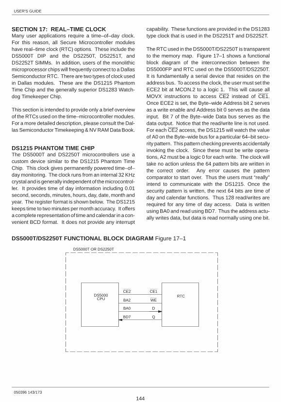
USER’S GUIDE
050396 143/173
144
SECTION 17: REAL–TIME CLOCKMany user applications require a time–of–day clock.For this reason, all Secure Microcontroller moduleshave real–time clock (RTC) options. These include theDS5000T DIP and the DS2250T, DS2251T, andDS2252T SIMMs. In addition, users of the monolithicmicroprocessor chips will frequently connect to a DallasSemiconductor RTC. There are two types of clock usedin Dallas modules. These are the DS1215 PhantomTime Chip and the generally superior DS1283 Watch-dog Timekeeper Chip.
This section is intended to provide only a brief overviewof the RTCs used on the time–microcontroller modules.For a more detailed description, please consult the Dal-las Semiconductor Timekeeping & NV RAM Data Book.
DS1215 PHANTOM TIME CHIPThe DS5000T and DS2250T microcontrollers use acustom device similar to the DS1215 Phantom TimeChip. This clock gives permanently powered time–of–day monitoring. The clock runs from an internal 32 KHzcrystal and is generally independent of the microcontrol-ler. It provides time of day information including 0.01second, seconds, minutes, hours, day, date, month andyear. The register format is shown below. The DS1215keeps time to two minutes per month accuracy. It offersa complete representation of time and calendar in a con-venient BCD format. It does not provide any interrupt
capability. These functions are provided in the DS1283type clock that is used in the DS2251T and DS2252T.
The RTC used in the DS5000T/DS2250T is transparentto the memory map. Figure 17–1 shows a functionalblock diagram of the interconnection between theDS5000FP and RTC used on the DS5000T/DS2250T.It is fundamentally a serial device that resides on theaddress bus. To access the clock, the user must set theECE2 bit at MCON.2 to a logic 1. This will cause allMOVX instructions to access CE2 instead of CE1.Once ECE2 is set, the Byte–wide Address bit 2 servesas a write enable and Address bit 0 serves as the datainput. Bit 7 of the Byte–wide Data bus serves as thedata output. Notice that the read/write line is not used.For each CE2 access, the DS1215 will watch the valueof A0 on the Byte–wide bus for a particular 64–bit secu-rity pattern. This pattern checking prevents accidentallyinvoking the clock. Since these must be write opera-tions, A2 must be a logic 0 for each write. The clock willtake no action unless the 64 pattern bits are written inthe correct order. Any error causes the patterncomparator to start over. Thus the users must “really”intend to communicate with the DS1215. Once thesecurity pattern is written, the next 64 bits are time ofday and calendar functions. Thus 128 read/writes arerequired for any time of day access. Data is writtenusing BA0 and read using BD7. Thus the address actu-ally writes data, but data is read normally using one bit.
DS5000T/DS2250T FUNCTIONAL BLOCK DIAGRAM Figure 17–1
DS5000CPU
RTC
DS5000T OR DS2250T
CE2 CE1
BA2 WE
BA0 D
BD7 Q
USER’S GUIDE
050396 144/173
145
The timekeeper contains a shift register with 128 loca-tions. The first 64 locations correspond to a patternshown in Figure 17–2. The next 64 are time data. Be-fore access to time data may occur, the 64–bit patternmust be written. The incoming bits are checked by apattern recognition circuit. As each correct bit of the pat-tern is received, the pointer is advanced. Any incorrectbit will cause the pointer to stop, and it may only be resetby a read operation. When the 64 bits of the patternhave been correctly written, access to RTC data begins.The next 64 bits are time data according to Figure 17–4.When the 64 bits of time data have been read or written(each bit increments the pointer), the pointer has com-pleted its cycle of 128. The next time access is initiatedby writing the pattern again. The pointer should be resetwith a read operation, to set it to a known location.
To write a data bit to the RTC, a MOVX instruction thatforces A2 low and A0 to the state of the bit must be per-formed. All other address lines should be low. Addressline A2 can be thought of as the write enable to the clockand A0 as the input bit. Therefore, to write the 64 bits ofthe pattern recognition sequence, 64 MOVX instruc-tions must be executed. A read is performed in a similarmanner, but A2 is high. Notice that data is encoded intothe address line. Either a MOVX A, @DPTR or MOVX@DPTR, A will accomplish a write if the DPH contains00H, and DPL contains 0000000Xb. The data bit is A0.The R/W signal is irrelevant.
To read a data bit from the clock once the 64–bit patternhas been entered, a MOVX instruction (MOVX A, @Rior MOVX A, @DPTR) must be executed that sets A2 toa 1. The data bit desired will then be returned in bit 7 ofthe accumulator. Therefore, to retrieve the 8 bytes oftime information in the clock, 64 read MOVX instructionsmust be executed.
Since the clock pointer increments for each memory ac-cess (read or write), extra reads or writes must not beperformed (the pointer would move accidently). For thisreason, any interruption of the time read/write processshould close ECE2 immediately. An inadvertentmemory access to this space would move the pointer,and time data would appear to be garbage on returningto timekeeping. If possible, interrupts should be dis-abled when executing time transactions.
Note that the clock access is performed as a Byte–widememory access. The EA pin must remain high. If thispin is low, all memory access is directed outside the chipvia the expanded bus. Therefore, the timekeeper wouldbe outside the current memory map.
Figure 17–3 is a flowchart which summarizes how to ac-cess the time for retrieval and modification. Also, anapplication example at the end of this section lists a pro-gram which contains sample subroutines for communi-cating with the clock.
IMPORTANT APPLICATION NOTE
The ECE2 bit used to access the DS1215 on the DS5000T and DS2250T is non–volatile. If the processor is reset orpower is lost during an access to the RTC (while ECE2=1), it will maintain its state following reset. This unintentionalsetting of the ECE2 bit may interfere with MOVX instructions if software expects the bit to be cleared following reset.As a general precaution, it is recommended that the ECE2 bit be cleared as part of the reset routine of the device.

USER’S GUIDE
050396 145/173
146
PATTERN COMPARISON REGISTER DESCRIPTION Figure 17–2
7 6 5 4 3 2 1 0
10100011
01011100
11000101
00111010
10100011
01011100
11000101
00111010
BYTE 0
BYTE 1
BYTE 2
BYTE 3
BYTE 4
BYTE 5
BYTE 6
BYTE 7
HEXCODE
C5
3A
A3
5C
C5
3A
A3
5C

USER’S GUIDE
050396 146/173
147
DS1215 REGISTER ENTRY FLOWCHART Figure 17–3
Set ECE2 bit in the MCONregister to a logic 1
Perform a dummy readoperation to reset clock patternrecognition circuit*
To open clock, write the 64–bitserial pattern by using A2 andA0 embedded address lines
Are clock timeregisters to beread/written?
Read time registers one bit ata time using read MOVXinstructions that set A2 tologic 1. Bit to be read willbe returned in bit 7 of databyte.
Clear ECE2 to a zero toaccess normal embedded
data memory map
* To guarantee that the pattern recognition circuit isreset to the first bit of the sequence it is highly rec-ommended that 65 read operations be performed.This is in case the DS5000T has been interruptedor reset while the clock was open.
Write to time registers one bitat a time using write MOVXinstructions that clear A2 to a logic 0. A0 should be the bitto be written.
Read
Written
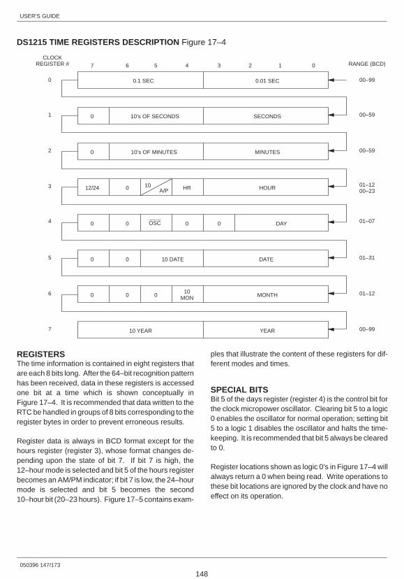
USER’S GUIDE
050396 147/173
148
DS1215 TIME REGISTERS DESCRIPTION Figure 17–4
OSC
7 6 5 4 3 2 1 0
0.1 SEC
0
0
HR012/24
0000
00
000
10 YEAR
RANGE (BCD)
00–99
00–59
00–59
01–12
01–07
01–31
01–12
00–99
CLOCK
0
1
2
3
4
5
6
7
REGISTER #
0.01 SEC
10’s OF SECONDS SECONDS
10’s OF MINUTES MINUTES
10A/P HOUR
DAY
10 DATE DATE
10MON MONTH
YEAR
00–23
REGISTERSThe time information is contained in eight registers thatare each 8 bits long. After the 64–bit recognition patternhas been received, data in these registers is accessedone bit at a time which is shown conceptually inFigure 17–4. It is recommended that data written to theRTC be handled in groups of 8 bits corresponding to theregister bytes in order to prevent erroneous results.
Register data is always in BCD format except for thehours register (register 3), whose format changes de-pending upon the state of bit 7. If bit 7 is high, the12–hour mode is selected and bit 5 of the hours registerbecomes an AM/PM indicator; if bit 7 is low, the 24–hourmode is selected and bit 5 becomes the second10–hour bit (20–23 hours). Figure 17–5 contains exam-
ples that illustrate the content of these registers for dif-ferent modes and times.
SPECIAL BITSBit 5 of the days register (register 4) is the control bit forthe clock micropower oscillator. Clearing bit 5 to a logic0 enables the oscillator for normal operation; setting bit5 to a logic 1 disables the oscillator and halts the time-keeping. It is recommended that bit 5 always be clearedto 0.
Register locations shown as logic 0’s in Figure 17–4 willalways return a 0 when being read. Write operations tothese bit locations are ignored by the clock and have noeffect on its operation.

USER’S GUIDE
050396 148/173
149
TIME REGISTER EXAMPLES Figure 17–5
7 6 5 4 3 2 1 0
0
0
101
0000
00
000
RANGE (BCD)
00–99
00–59
00–59
01–12
01–07
01–31
01–12
00–99
CLOCK
0
1
2
3
4
5
6
7
REGISTER #
1 0 0 0 1 0 0 1
1 0 1 0 0 0 1
0 0 1 0 0 1 0
1 0 0 0 1
0 0 0 1
1 1 0 0 0 0
1 0 0 0 0
001 0 1 0 0 0
The time indicated is 11 o’clock PM, 12 minutes, 51.89 seconds. The date indicated is Sunday, October 30th, 1988.
0
0
000
0000
00
000
00–99
00–59
00–59
01–12
01–07
01–31
01–12
00–99
0
1
2
3
4
5
6
7
1 0 0 0 1 0 0 1
1 0 1 0 0 0 1
1 0 1 1 0 0 1
1 0 0 1 1
0 0 1 0
1 0 0 0 1 0
1 0 0 0 1
001 0 1 0 0 0
The time indicated is 2300 hour, 59 minutes, 51.89 seconds. The date indicated is Monday, November 22nd, 1988.
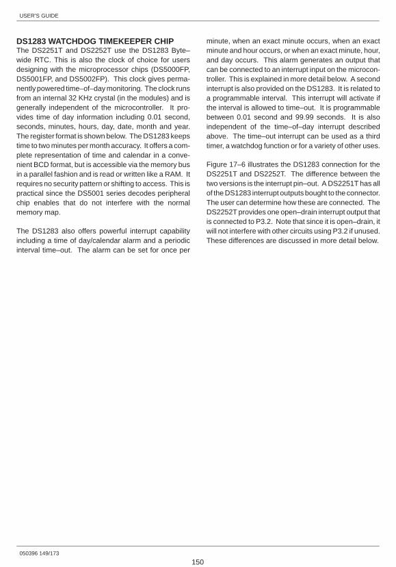
USER’S GUIDE
050396 149/173
150
DS1283 WATCHDOG TIMEKEEPER CHIPThe DS2251T and DS2252T use the DS1283 Byte–wide RTC. This is also the clock of choice for usersdesigning with the microprocessor chips (DS5000FP,DS5001FP, and DS5002FP). This clock gives perma-nently powered time–of–day monitoring. The clock runsfrom an internal 32 KHz crystal (in the modules) and isgenerally independent of the microcontroller. It pro-vides time of day information including 0.01 second,seconds, minutes, hours, day, date, month and year.The register format is shown below. The DS1283 keepstime to two minutes per month accuracy. It offers a com-plete representation of time and calendar in a conve-nient BCD format, but is accessible via the memory busin a parallel fashion and is read or written like a RAM. Itrequires no security pattern or shifting to access. This ispractical since the DS5001 series decodes peripheralchip enables that do not interfere with the normalmemory map.
The DS1283 also offers powerful interrupt capabilityincluding a time of day/calendar alarm and a periodicinterval time–out. The alarm can be set for once per
minute, when an exact minute occurs, when an exactminute and hour occurs, or when an exact minute, hour,and day occurs. This alarm generates an output thatcan be connected to an interrupt input on the microcon-troller. This is explained in more detail below. A secondinterrupt is also provided on the DS1283. It is related toa programmable interval. This interrupt will activate ifthe interval is allowed to time–out. It is programmablebetween 0.01 second and 99.99 seconds. It is alsoindependent of the time–of–day interrupt describedabove. The time–out interrupt can be used as a thirdtimer, a watchdog function or for a variety of other uses.
Figure 17–6 illustrates the DS1283 connection for theDS2251T and DS2252T. The difference between thetwo versions is the interrupt pin–out. A DS2251T has allof the DS1283 interrupt outputs bought to the connector.The user can determine how these are connected. TheDS2252T provides one open–drain interrupt output thatis connected to P3.2. Note that since it is open–drain, itwill not interfere with other circuits using P3.2 if unused.These differences are discussed in more detail below.
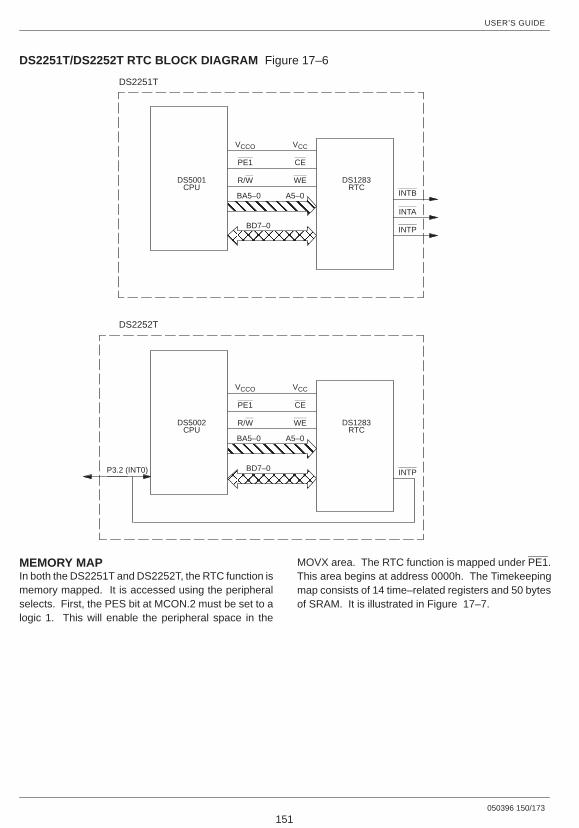
USER’S GUIDE
050396 150/173
151
DS2251T/DS2252T RTC BLOCK DIAGRAM Figure 17–6
ÇÇÇÇÇÇÇÇÇÇÇÇ
DS5001CPU
DS1283RTC
DS2251T
VCCO VCC
PE1 CE
R/W WE
ÑÑÑÑÑÑÑÑÑÑÑÑ
BA5–0 A5–0
BD7–0
INTB
INTA
INTP
ÇÇÇÇÇÇÇÇÇÇÇÇ
DS5002CPU
DS1283RTC
DS2252T
VCCO VCC
PE1 CE
R/W WE
ÑÑÑÑÑÑÑÑÑÑÑÑ
BA5–0 A5–0
BD7–0 INTPP3.2 (INT0)
MEMORY MAPIn both the DS2251T and DS2252T, the RTC function ismemory mapped. It is accessed using the peripheralselects. First, the PES bit at MCON.2 must be set to alogic 1. This will enable the peripheral space in the
MOVX area. The RTC function is mapped under PE1.This area begins at address 0000h. The Timekeepingmap consists of 14 time–related registers and 50 bytesof SRAM. It is illustrated in Figure 17–7.
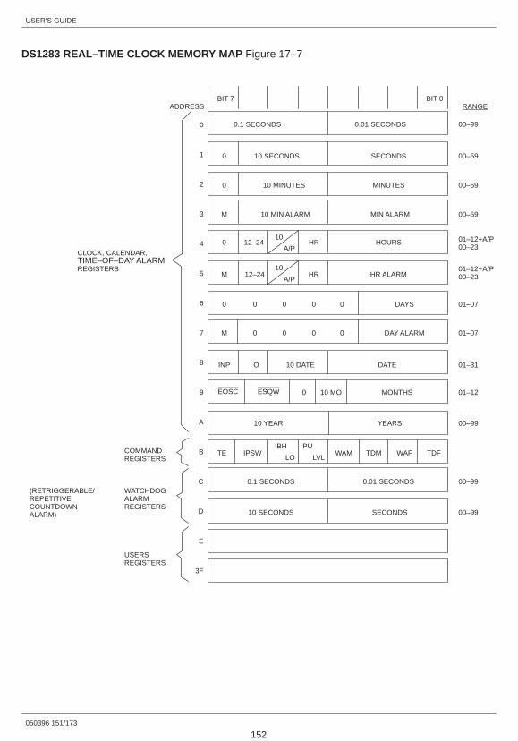
USER’S GUIDE
050396 151/173
152
DS1283 REAL–TIME CLOCK MEMORY MAP Figure 17–7
0.1 SECONDS 0.01 SECONDS
0 10 SECONDS SECONDS
MINUTES10 MINUTES0
M 10 MIN ALARM MIN ALARM
0 12–2410
A/PHR HOURS
M 12–2410
A/PHR HR ALARM
0 0 0 0 0 DAYS
M 0 0 0 0 DAY ALARM
INP O 10 DATE DATE
EOSC ESQW 0 10 MO MONTHS
10 YEAR YEARS
TE IPSW WAM TDM WAF TDFIBH PU
LO LVL
0.1 SECONDS 0.01 SECONDS
10 SECONDS SECONDS
00–99
00–59
00–59
00–59
01–12+A/P00–23
01–12+A/P00–23
01–07
01–07
01–31
01–12
00–99
00–99
00–99
0
1
2
3
4
5
6
7
8
9
A
B
C
D
E
3F
RANGEBIT 7 BIT 0
ADDRESS
CLOCK, CALENDAR,TIME–OF–DAY ALARMREGISTERS
COMMANDREGISTERS
WATCHDOGALARMREGISTERS
USERSREGISTERS
(RETRIGGERABLE/REPETITIVECOUNTDOWNALARM)

USER’S GUIDE
050396 152/173
153
The time, calendar, and alarms are controlled by theinformation in these 14 registers. In particular, the Com-mand register controls most functions. This is describedin Figure 17–8. There are two additional bits thatdeserve mention. These reside in the register ataddress 09h. Bit 7 is EOSC, which enables the Time-keeping oscillator if set to a 0. Battery lifetime can bepreserved by disabling the oscillator when it is notneeded and power is not present. Note the user’s soft-
ware should enable the oscillator, as it should be off forshipping. If the oscillator is off, a user can read or writeto the Timekeeping register, but the time value will notchange. Bit 6 of the same register is the ESQW bit. Thiscontrols the timekeeper 1024 Hz SQW output. TheSQW signal is available on the DS2251T. When it isenabled, it drives a square wave of 1024 Hz. When dis-abled, it is tri–state so it will not interfere with other usesof a port pin.
DS1283 REAL–TIME CLOCK COMMAND REGISTER Figure 17–8
RTC COMMAND Register Address 0BH
TE IPSW IBH/L0 PU/LVL WAM TDM WAF TDF
CMD.7: TE
Transfer Enable To avoid updating of time registers while a read is taking place, the updatemay be frozen. Setting the TE bit to a logic 0 will prevent an update of theuser–readable registers from the actual time of day. Setting TE to a logic 1will enable updates every 0.01 seconds.
CMD.6: IPSW
Interrupt Switch When set to a logic 1, INTP will be assigned to time of day alarm and INTBwill be assigned to the periodic time–out. When set to a logic 0, the functionsare reversed.
CMD.5: IBHL
INTB H/L When set to logic 1, the INTB will source current (active high). When set to alogic 0, INTB will sink current (active low).
CMD.4: PU/LVL
Pulse/Level When set to a logic 1, INTP will sink current for approximately 3 ms when it isactivated. INTB will sink or source (as set by IBLH) for 3 ms. When set to alogic 0, the interrupt pins will signal with a continuous level.
CMD.3: WAM
Watchdog Alarm When set to a logic 1, the watchdog countdown timer interrupt will beMask disabled. When set to a logic 0, the countdown interrupt is enabled.
CMD.2: TDM
Time of Day When set to a logic 1, the time of day interrupt is disabled. When set to aAlarm Mask logic 0, the time of day alarm is enabled.
CMD.1: WAF
Watchdog This bit will be set to a logic 1 by the DS1283 when a watchdog time–outAlarm Flag occurs. WAF is reset by reading or writing either of the countdown registers.
CMD.0: TDF
Time of Day This bit is set to a logic 1 by the DS1283 when a time of day alarm occurs. It isAlarm Flag cleared by reading or writing any time of day alarm register (register 3, 5, or 7).
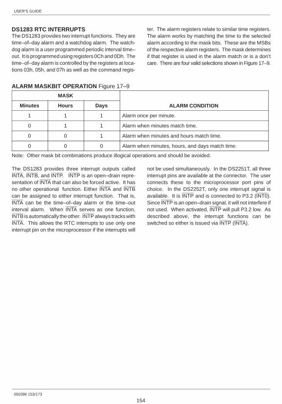
USER’S GUIDE
050396 153/173
154
DS1283 RTC INTERRUPTSThe DS1283 provides two interrupt functions. They aretime–of–day alarm and a watchdog alarm. The watch-dog alarm is a user programmed periodic interval time–out. It is programmed using registers 0Ch and 0Dh. Thetime–of–day alarm is controlled by the registers at loca-tions 03h, 05h, and 07h as well as the command regis-
ter. The alarm registers relate to similar time registers.The alarm works by matching the time to the selectedalarm according to the mask bits. These are the MSBsof the respective alarm registers. The mask determinesif that register is used in the alarm match or is a don’tcare. There are four valid selections shown in Figure 17–9.
ALARM MASKBIT OPERATION Figure 17–9
MASK
Minutes Hours Days ALARM CONDITION
1 1 1 Alarm once per minute.
0 1 1 Alarm when minutes match time.
0 0 1 Alarm when minutes and hours match time.
0 0 0 Alarm when minutes, hours, and days match time.
Note: Other mask bit combinations produce illogical operations and should be avoided.
The DS1283 provides three interrupt outputs calledINTA, INTB, and INTP. INTP is an open–drain repre-sentation of INTA that can also be forced active. It hasno other operational function. Either INTA and INTBcan be assigned to either interrupt function. That is,INTA can be the time–of–day alarm or the time–outinterval alarm. When INTA serves as one function,INTB is automatically the other. INTP always tracks withINTA. This allows the RTC interrupts to use only oneinterrupt pin on the microprocessor if the interrupts will
not be used simultaneously. In the DS2251T, all threeinterrupt pins are available at the connector. The userconnects these to the microprocessor port pins ofchoice. In the DS2252T, only one interrupt signal isavailable. It is INTP and is connected to P3.2 (INT0).Since INTP is an open–drain signal, it will not interfere ifnot used. When activated, INTP will pull P3.2 low. Asdescribed above, the interrupt functions can beswitched so either is issued via INTP (INTA).
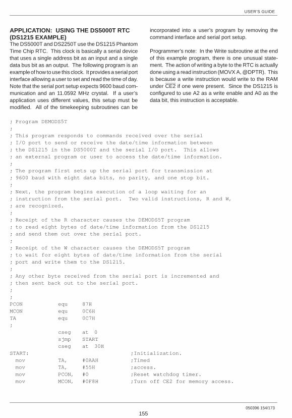
USER’S GUIDE
050396 154/173
155
APPLICATION: USING THE DS5000T RTC(DS1215 EXAMPLE)The DS5000T and DS2250T use the DS1215 PhantomTime Chip RTC. This clock is basically a serial devicethat uses a single address bit as an input and a singledata bus bit as an output. The following program is anexample of how to use this clock. It provides a serial portinterface allowing a user to set and read the time of day.Note that the serial port setup expects 9600 baud com-munication and an 11.0592 MHz crystal. If a user’sapplication uses different values, this setup must bemodified. All of the timekeeping subroutines can be
incorporated into a user’s program by removing thecommand interface and serial port setup.
Programmer’s note: In the Write subroutine at the endof this example program, there is one unusual state-ment. The action of writing a byte to the RTC is actuallydone using a read instruction (MOVX A, @DPTR). Thisis because a write instruction would write to the RAMunder CE2 if one were present. Since the DS1215 isconfigured to use A2 as a write enable and A0 as thedata bit, this instruction is acceptable.
; Program DEMODS5T;; This program responds to commands received over the serial; I/O port to send or receive the date/time information between; the DS1215 in the DS5000T and the serial I/O port. This allows; an external program or user to access the date/time information.;; The program first sets up the serial port for transmission at; 9600 baud with eight data bits, no parity, and one stop bit.;; Next, the program begins execution of a loop waiting for an; instruction from the serial port. Two valid instructions, R and W,; are recognized.;; Receipt of the R character causes the DEMODS5T program; to read eight bytes of date/time information from the DS1215; and send them out over the serial port.;; Receipt of the W character causes the DEMODS5T program; to wait for eight bytes of date/time information from the serial; port and write them to the DS1215.;; Any other byte received from the serial port is incremented and; then sent back out to the serial port.;;PCON equ 87HMCON equ 0C6HTA equ 0C7H;
cseg at 0sjmp STARTcseg at 30H
START: ;Initialization.mov TA, #0AAH ;Timedmov TA, #55H ;access.mov PCON, #0 ;Reset watchdog timer.mov MCON, #0F8H ;Turn off CE2 for memory access.

USER’S GUIDE
050396 155/173
156
lcall CLOSE ;Close date/time registers.
mov IE, #0mov TMOD, #20H ;Initialize themov TH1, #0FAH ;serial portmov TL1, #0FAH ;for 9600orl PCON, #80H ;baud using 11.0592 MHz crystal.mov SCON, #52Hmov TCON, #40H
L:jnb RI, L ;Wait for character.clr RI ;Clear the receiver.mov A, SBUF ;Load in the character.cjne A, #’R, H ;Skip if not a read.lcall OPEN ;Set up to read date/time.mov B #8 ;Set up to send 8 bytes.
F:lcall RBYTE ;Read a byte of date/time.
G:jnb TI, G ;Wait for end of previous send.clr TI ;Clear transmitter.mov SBUF, A ;Send out the byte.djnz B, F ;Loop for 8 bytes.sjmp L ;Return to main loop.
H:cjne A, #’W’, J ;Skip if not a write.lcall OPEN ;Set up to read date/time.mov B, #8 ; Set up to receive 8 bytes.
I:jnb RI, I ;Wait to receive a byte.clr RI ;Clear the receiver.mov A, SBUF ;Bring in the byte.lcall WBYTE ;Write a byte of date/time.djnz B, I ;Loop for 8 bytes.sjmp L ;Return to main loop.
J:jnb TI, J ;If it is neither an R nor a Wclr TI ;increment the character,inc A ;send it back out to themov SBUF, A ;serial port, and thensjmp L ;return to the main loop.
;;; SUBROUTINE TO OPEN THE CLOCK/CALENDAR (ECC);; This subroutine executes the sequence of reads and writes which; is required in order to open communication with the timekeeper.; The subroutine returns with the timekeeper opened for data; access with both the accumulator and B register modified.;

USER’S GUIDE
050396 156/173
157
OPEN: LCALL CLOSE ;Make sure it is closed.MOV B,#4 ;Set pattern period count.MOV A,#0C5H ;Load first byte of pattern.
OPENA: LCALL WBYTE ;Send out the byte.XRL A,#0FFH ;Generate next pattern byte.LCALL WBYTE ;Send out the byte.SWAP A ;Generate next pattern byte.DJNZ B,OPENA ;Repeat until 8 bytes sent.RET ;Return.
;;********************************;*** SUBROUTINE TO CLOSE THE RTC;********************************;; This subroutine insures that the registers of the timekeeper; are closed by executing 9 successive reads of the date and time; registers. The subroutine returns with both the accumulator; and the B register modified.;CLOSE: MOV B,#9 ;Set up to read 9 bytes.CLOSEA: LCALL RBYTE ;Read a byte.
DJNZ B,CLOSEA ;Loop for 9 byte reads.RET ;Return.
;;***********************************;*** SUBROUTINE TO READ A DATA BYTE;***********************************;; This subroutine performs a “context switch: to the CE2 data; space and then reads one byte from the timekeeping device.; Then it switches back to the CE1 data space and returns; the byte read in the accumulator, with all other registers; unchanged.;RBYTE: PUSH DPL ;Save the data
PUSH DPH ; pointer on stack.PUSH MCON ;Save MCON register.ORL MCON,#4 ;Switch to CE2.PUSH B ;Save the B register.MOV DPL,#4 ;Set up for data input.MOV DPH,#0 ;Set high address byte.MOV B,#8 ;Set the bit count.
LI: PUSH ACC ;Save the accumulator.MOVX A,@DPTR ;Input the data bit from the RTC into
; ACC.7.RLC A ;Move it to carry.POP ACC ;Get the accumulator.RRC A ;Save the data bit.DJNZ B,LI ;Loop for a whole byte.POP B ;Restore the B register.POP MCON ;Restore the MCON register.
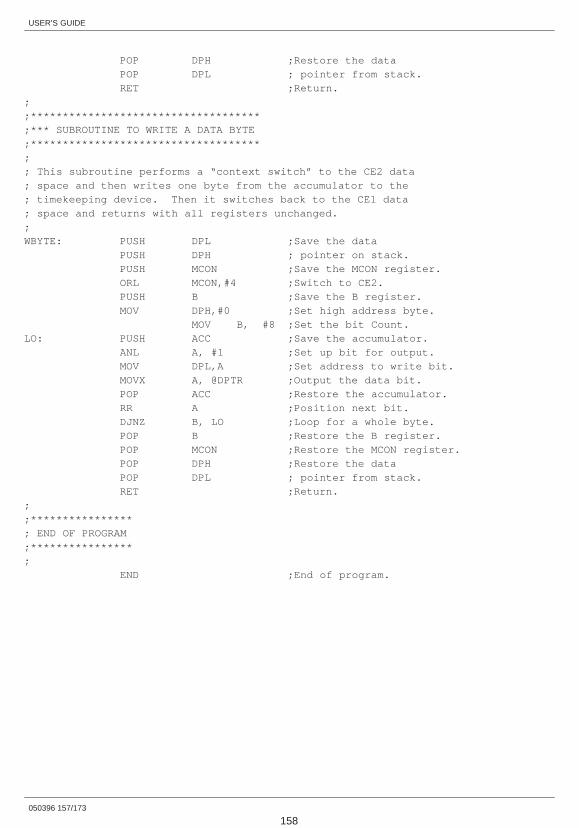
USER’S GUIDE
050396 157/173
158
POP DPH ;Restore the dataPOP DPL ; pointer from stack.RET ;Return.
;;************************************;*** SUBROUTINE TO WRITE A DATA BYTE;************************************;; This subroutine performs a “context switch” to the CE2 data; space and then writes one byte from the accumulator to the; timekeeping device. Then it switches back to the CE1 data; space and returns with all registers unchanged.;WBYTE: PUSH DPL ;Save the data
PUSH DPH ; pointer on stack.PUSH MCON ;Save the MCON register.ORL MCON,#4 ;Switch to CE2.PUSH B ;Save the B register.MOV DPH,#0 ;Set high address byte.
MOV B, #8 ;Set the bit Count.LO: PUSH ACC ;Save the accumulator.
ANL A, #1 ;Set up bit for output.MOV DPL,A ;Set address to write bit.MOVX A, @DPTR ;Output the data bit.POP ACC ;Restore the accumulator.RR A ;Position next bit.DJNZ B, LO ;Loop for a whole byte.POP B ;Restore the B register.POP MCON ;Restore the MCON register.POP DPH ;Restore the dataPOP DPL ; pointer from stack.RET ;Return.
;;****************; END OF PROGRAM;****************;
END ;End of program.
USER’S GUIDE
050396 158/173
159
APPLICATION: USING THE DS2251T RTC(DS1283 EXAMPLE)The DS2251T or DS2252T use the DS1283 Byte–widetype real–time clock (RTC). This clock is accessed in aparallel fashion like a RAM. The user simply writes to theregisters to set the time and control functions. The fol-lowing program is an example of how to use this clock. Itprovides a serial port interface allowing an user to set
and read the time of day. Note that the serial port setupexpects 9600 baud communication and an 11.0592MHz crystal. If a user’s application uses different val-ues, this setup must be modified. All of the timekeepingaccess is performed in the code under Set Time and TellTime. The remainder of this program concerns gettingdata in and out of the serial port for display purposesand has nothing to do with timekeeper access.
; Program DS1283;; This program responds to commands received over the serial; port to set the date and time information in the DS1283;; The program first initializes the serial port for communication; at 9600 baud with eight data bits, no parity, and one stop bit.;; After setting the date and time, the program begins execution; of an infinite loop which sends back the date and time each; time a character is received.;CR EQU 0DHLF EQU 0AH;MCON EQU 0C6HTA EQU 0C7H CSEG AT 0; MOV TA, #0AAH ; Timed MOV TA, #55H ; access. MOV PCON, #0 ; Reset watchdog timer. ANL MCON, #0FBH ; Turn off PES for memory access. MOV P2, #0 ; Clear high byte of address.
; for clock access; MOV IE, #0 MOV TMOD, #20H ; Initialize the MOV TH1, #0FAH ; serial port MOV TL1, #0FAH ; for 9600 ORL PCON, #80H ; baud, with 11.0522 MHz crystal. MOV SCON, #52H MOV TCON, #40H
;Messages MOV DPTR, #TEXT0 LCALL TEXT_OUT LCALL CHAR_IN LCALL CHAR_OUT PUSH ACC MOV DPTR, #TEXT3 LCALL TEXT_OUT POP ACC ANL A, #5FH CJNE A, #’Y’, TELL_TIME
USER’S GUIDE
050396 159/173
160
;Set Time CLR A MOV R0, #0Bh LCALL WBYTE ; Freeze the registers. MOV DPTR, #YEAR LCALL TEXT_OUT LCALL HEX_IN LCALL WBYTE ; Set the year. MOV DPTR, #MONTH LCALL TEXT_OUT LCALL HEX_IN LCALL WBYTE ; Set the month. MOV DPTR, #DAY LCALL TEXT_OUT LCALL HEX_IN LCALL WBYTE ; Set the day. DEC R0 MOV DPTR, #DAYW LCALL TEXT_OUT LCALL HEX_IN LCALL WBYTE ; Set day of the week. DEC R0 MOV DPTR, #HOUR LCALL TEXT_OUT LCALL HEX_IN LCALL WBYTE ; Set the hour. DEC R0 MOV DPTR, #MINUTE LCALL TEXT_OUT LCALL HEX_IN LCALL WBYTE ; Set the minute. CLR A LCALL WBYTE ; Set seconds LCALL WBYTE ; to 00.00 MOV DPTR, #TRIGGER LCALL TEXT_OUT LCALL CHAR_IN ; Wait for trigger. MOV A, #80H MOV R0, #11 LCALL WBYTE ; Un–freeze the registers.;TELL_TIME: MOV DPTR, #TEXT4 LCALL TEXT_OUT ; Invite user to read time.CONTINUE:; LCALL CHAR_IN ; Wait for read request. CLR A MOV R0, #11 LCALL WBYTE ; Freeze the registers. MOV DPTR, #TEXT1 LCALL TEXT_OUT MOV R0, #9 LCALL RBYTE ; Read the month. ANL A, #1FH ; Isolate it. LCALL HEX_OUT ; Display month. MOV A, #’/’ LCALL CHAR_OUT
USER’S GUIDE
050396 160/173
161
LCALL RBYTE ; Read the day of month. ANL A, #3FH ; Isolate it. LCALL HEX_OUT ; Display day of month. MOV A, #’/’ LCALL CHAR_OUT MOV R0, #10 LCALL RBYTE ; Read the year. LCALL HEX_OUT ; Display the year. MOV DPTR, #TEXT2 LCALL TEXT_OUT MOV R0, #4 LCALL RBYTE ; Read the hour. DEC R0 LCALL HEX_OUT ; Display the hour. MOV A, #’:’ LCALL CHAR_OUT LCALL RBYTE ; Read the minute. LCALL HEX_OUT ; Display the minute. MOV A, #’:’ LCALL CHAR_OUT LCALL RBYTE ; Read the second. LCALL HEX_OUT ; Display the second. MOV A, #’.’ LCALL CHAR_OUT LCALL RBYTE ; Read fraction of second. LCALL HEX_OUT ; Display fraction of second. MOV DPTR, #TEXT3 LCALL TEXT_OUT MOV A, #80H MOV R0, #11 LCALL WBYTE ; Un–freeze the registers.; SJMP CONTINUE ; Repeat indefinitely.;;Utilities
HEX_IN: MOV B, #0HEX_LP: LCALL CHAR_IN LCALL CHAR_OUT CJNE A, #0DH, NOT_CR MOV A, B RETNOT_CR: ADD A, #–30H JNC HEX_LP CJNE A, #10, $+3 JC HEX_XX ADD A, #–7 CJNE A, #10, $+3 JC HEX_LP CJNE A, #16, $+3 JNC HEX_LPHEX_XX: XCH A, B ANL A, #0FH SWAP A
USER’S GUIDE
050396 161/173
162
ORL A, B MOV B, A SJMP HEX_LP;HEX_OUT: MOV B, #2OUT_LP: SWAP A PUSH ACC ANL A, #0FH CJNE A, #10, $+3 JC HEX_OK ADD A, #7HEX_OK: ADD A, #30H LCALL CHAR_OUT POP ACC DJNZ B, OUT_LP RET;TEXT_OUT: PUSH ACCWT1: CLR A MOVC A, @A+DPTR INC DPTR JZ WT2 LCALL CHAR_OUT SJMP WT1WT2: POP ACC RET;CHAR_IN: JNB RI, CHAR_IN MOV A, SBUF CLR RI RET;CHAR_OUT: JNB TI, CHAR_OUT MOV SBUF, A CLR TI RET;RBYTE: PUSH MCON ; Save MCON register. ORL MCON, #4 ; Switch to PES. MOVX A, @R0 ; Read the register. DEC R0 ; Decrement the pointer. POP MCON ; Restore MCON register. RET ; Return.;WBYTE: PUSH MCON ; Save MCON register. ORL MCON, #4 ; Switch to PES. MOVX @R0, A ; Read the register. DEC R0 ; Decrement the pointer.
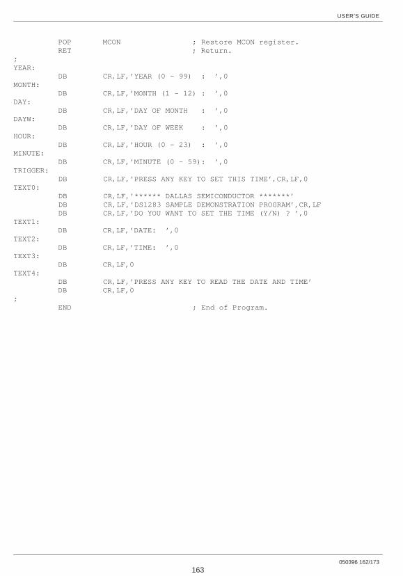
USER’S GUIDE
050396 162/173
163
POP MCON ; Restore MCON register. RET ; Return.;YEAR: DB CR,LF,’YEAR (0 – 99) : ’,0MONTH: DB CR,LF,’MONTH (1 – 12) : ’,0DAY: DB CR,LF,’DAY OF MONTH : ’,0DAYW: DB CR,LF,’DAY OF WEEK : ’,0HOUR: DB CR,LF,’HOUR (0 – 23) : ’,0MINUTE: DB CR,LF,’MINUTE (0 – 59): ’,0TRIGGER: DB CR,LF,’PRESS ANY KEY TO SET THIS TIME’,CR,LF,0TEXT0: DB CR,LF,’****** DALLAS SEMICONDUCTOR *******’ DB CR,LF,’DS1283 SAMPLE DEMONSTRATION PROGRAM’,CR,LF DB CR,LF,’DO YOU WANT TO SET THE TIME (Y/N) ? ’,0TEXT1: DB CR,LF,’DATE: ’,0TEXT2: DB CR,LF,’TIME: ’,0TEXT3: DB CR,LF,0TEXT4: DB CR,LF,’PRESS ANY KEY TO READ THE DATE AND TIME’ DB CR,LF,0; END ; End of Program.
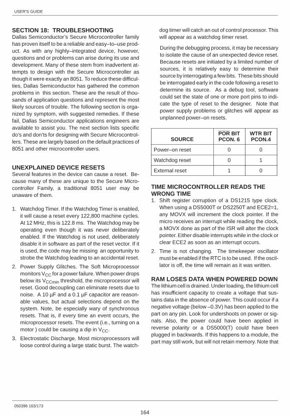
USER’S GUIDE
050396 163/173
164
SECTION 18: TROUBLESHOOTINGDallas Semiconductor’s Secure Microcontroller familyhas proven itself to be a reliable and easy–to–use prod-uct. As with any highly–integrated device, however,questions and or problems can arise during its use anddevelopment. Many of these stem from inadvertent at-tempts to design with the Secure Microcontroller asthough it were exactly an 8051. To reduce these difficul-ties, Dallas Semiconductor has gathered the commonproblems in this section. These are the result of thou-sands of application questions and represent the mostlikely sources of trouble. The following section is orga-nized by symptom, with suggested remedies. If thesefail, Dallas Semiconductor applications engineers areavailable to assist you. The next section lists specificdo’s and don’ts for designing with Secure Microcontrol-lers. These are largely based on the default practices of8051 and other microcontroller users.
UNEXPLAINED DEVICE RESETSSeveral features in the device can cause a reset. Be-cause many of these are unique to the Secure Micro-controller Family, a traditional 8051 user may beunaware of them.
1. Watchdog Timer. If the Watchdog Timer is enabled,it will cause a reset every 122,800 machine cycles.At 12 MHz, this is 122.8 ms. The Watchdog may beoperating even though it was never deliberatelyenabled. If the Watchdog is not used, deliberatelydisable it in software as part of the reset vector. If itis used, the code may be missing an opportunity tostrobe the Watchdog leading to an accidental reset.
2. Power Supply Glitches. The Soft Microprocessormonitors VCC for a power failure. When power dropsbelow its VCCmin threshold, the microprocessor willreset. Good decoupling can eliminate resets due tonoise. A 10 µF and a 0.1 µF capacitor are reason-able values, but actual selections depend on thesystem. Note, be especially wary of synchronousresets. That is, if every time an event occurs, themicroprocessor resets. The event (i.e., turning on amotor ) could be causing a dip in VCC.
3. Electrostatic Discharge. Most microprocessors willloose control during a large static burst. The watch-
dog timer will catch an out of control processor. Thiswill appear as a watchdog timer reset.
During the debugging process, it may be necessaryto isolate the cause of an unexpected device reset.Because resets are initiated by a limited number ofsources, it is relatively easy to determine theirsource by interrogating a few bits. These bits shouldbe interrogated early in the code following a reset todetermine its source. As a debug tool, softwarecould set the state of one or more port pins to indi-cate the type of reset to the designer. Note thatpower supply problems or glitches will appear asunplanned power–on resets.
SOURCEPOR BITPCON. 6
WTR BITPCON.4
Power–on reset 0 0
Watchdog reset 0 1
External reset 1 0
TIME MICROCONTROLLER READS THEWRONG TIME1. Shift register corruption of a DS1215 type clock.
When using a DS5000T or DS2250T and ECE2=1,any MOVX will increment the clock pointer. If themicro receives an interrupt while reading the clock,a MOVX done as part of the ISR will alter the clockpointer. Either disable interrupts while in the clock orclear ECE2 as soon as an interrupt occurs.
2. Time is not changing. The timekeeper oscillatormust be enabled if the RTC is to be used. If the oscil-lator is off, the time will remain as it was written.
RAM LOSES DATA WHEN POWERED DOWNThe lithium cell is drained. Under loading, the lithium cellhas insufficient capacity to create a voltage that sus-tains data in the absence of power. This could occur if anegative voltage (below –0.3V) has been applied to thepart on any pin. Look for undershoots on power or sig-nals. Also, the power could have been applied inreverse polarity or a DS5000(T) could have beenplugged in backwards. If this happens to a module, thepart may still work, but will not retain memory. Note that

USER’S GUIDE
050396 164/173
165
lithium batteries have a very long time constant. Puttingthe device on the shelf for one to two weeks may restoreenough voltage to battery back the memory again. Thelifetime of such a battery will be reduced, however.
UNABLE TO INVOKE STOP MODEUnlike the 8051, the STOP bit in the PCON register isTimed Access protected. Existing 8051 code will notuse the Timed Access procedure, so the STOP modewould not be successfully invoked.
SERIAL PORT DOES NOT WORKThe serial port is not a complicated peripheral, but thereare many elements that need to be initialized. The fol-lowing checklist is provided to help in debugging.
1. Are the P3.0 (RXD) and P3.1 (TXD) bits in the Port3 SFR latch set to 1?
2. Is the correct serial port mode selected?
3. If using serial port mode 1 or 3, is appropriate timerreload value selected?
4. If using serial port mode 1 or 3, is timer 1 enabled?(TCON.6)
5. If desired, is the serial port doubler bit, SMOD, set?(PCON.7)
6. If desired, is the receiver enable bit, REN, set?(SCON.4)
7. Is the serial port interrupt bit, ES, set? (IE.4)
8. Is the global interrupt enable bit, EA, set? (IE.7)
PROGRAM WILL NOT EXECUTEThis is a general category of complaint. In most casesmore information is needed. Prior to calling for applica-tions support, check the status of ALE, PSEN, XTAL2,Ports, and RST. Also, try adding instructions that write avalue to the ports to see which sections of code arebeing run and which are not (similar to using print state-ments). The following is a list of some common reasonsthat the program will not execute.
EA is floatingThe EA pin has an internal pull down resistor. If EA isallowed to float, it assumes an active state which pre-vents using NV RAM. When EA=0, the device will usethe Expanded Bus on Ports 0 and 2. Connect EA directlyto +5V for proper operation.
Crystal is not runningCheck the capacitance used with the crystals. Approxi-mately 20–40 pF is typical. Take note of any straycapacitance that could increase the actual loading.
Memory map is not configuredIf the developer has not used the Bootstrap Loader toselect the correct memory map, it may be incompatiblewith the software. For example, a DS2251 with 64K ofmemory could be configured with a 32K range. Codeabove 32K in NV RAM would not be executed.
No StackC programmers frequently use a large memory model.This places the C stack in MOVX RAM area. The typicaldefault address for compilers is to place the stack at0000h. A device in a Partitionable mode will not haveMOVX NV RAM begin at 0000h. The C start up configu-ration should be altered to put the stack and any otherdata variables above the Partition. C programs will typi-cally crash if there is no stack.
Code is written for an 8052The 8052 family has 256 bytes of on chip RAM and athird timer. Secure Microcontroller family devices are8051 derivatives and do not have these resources.
Watchdog is running and unsupportedIf the Watchdog is enabled but not supported by soft-ware, it will reset the microprocessor at intervals of122.8 ms with a 12 MHz crystal. If writing to an LCD dis-play or similar activity, the initialization may take moretime that this. The code would appear not to run sincethe display would never get it message printed. Makecertain the Watchdog is either supported or disabled insoftware.
The CRC bit is set on a DS5001If the CRC bit is set, the DS5001 CPU will invoke theBootstrap Loader on each power up and perform aCRC. If the answer does not match the stored value, theprocessor will remain in the loader mode. If the user hasinadvertently set this bit and is not actually using theCRC, it will surely be incorrect and will invoke the loaderon each power up. A program will seem to run (the inter-nal ROM checking the NV RAM) then stop.

USER’S GUIDE
050396 165/173
166
HIGH CURRENT DRAIN IN STOP MODESecure Microcontrollers draw approximately 80 µA ofICC in Stop mode. However, the EA pin has a resistiveload of between 40K to 125K ohms. If EA is connectedto +5V, this pin will draw between 40 µA to 125 µA. Thiscurrent can be eliminated by grounding the EA pin andlocking the device via the bootstrap loader. Whenlocked, internal logic disregards the state of EA. Since itis no longer connected to +5V, the device will only drawits very low ICC.
DATA IS LOST OR CORRUPTEDA common cause is that data in a DS2250–64 or aDS5000FP based system is lost between banks. TheECE2 bit was most likely left active when software wassupposed to write to CE1 memory. The opposite is alsopossible. When using the DS5000FP or DS2250(T)data crossing between CE1 and CE2 must be managedcarefully.
Another possible cause is electrostatic discharge(ESD). This can corrupt memory locations and/or dam-age to the device. For more information see ApplicationNote 93: Design Guidelines for Microcontrollers Incor-porating NV RAM, located in this Data Book.
INT0 IS STUCK LOW ON DS2252TThe DS2252T incorporates a DS1283 real–time clockwith interrupt capability. The INTP output of the DS1283is connected to the INTO pin of the DS5002FP micro-controller and also the INTO pin of the SIMM. If an RTCinterrupt occurs, this will pull the INTO signal low.
If the system is not expecting the INTO signal to beactive, this can appear as the INTO signal “stuck” low.Because the state of the DS1283 alarm is undefinedafter the freshness seal is broken, the device can powerup with the interrupt active, holding the INTO signal low.This condition can also occur if software accidentallyactivates the DS1283 alarm during normal operation, orif an alarm occurs during data retention mode. To clearthis condition, clear the DS1283 alarm (if desired) aspart of the power–on reset sequence.
DS5000TK KIT DOES NOT RESPOND TOKIT5K SOFTWARE1. VCC and GND must be supplied via the ribbon cable.
An external crystal (via ribbon cable) is required torun a program. The DS5000TK hardware internaloscillator is used only for program loading.
2. Cable is broken or a standard phone cable has beenused. A standard phone cable has the wrong pin outof the DS5000TK.
3. Incorrect COM port has been selected.
4. The device is not locked into its ZIF socket.
COMMUNICATION FAILS ON A DS5000TK1. The ribbon cable represents a significant stray
capacitance to the crystal pins. The crystal may berunning at the wrong frequency. This can bechecked by observing ALE which should be 1/6 ofthe crystal. If it is not, adjust the capacitors to get thecorrect frequency.
2. The A/B switch is in the wrong position. In positionA, the serial port is routed to the target system. Inposition B, it goes back to the PC COM port.
DEMODS5T PROGRAM DOESN’T WORKNormally due to the serial communication problemsmentioned above. For the demo, the crystal must oscil-late at 11.0592 MHz. Also, the A/B switch must be inposition B so the microcontroller communicates with thePC via the serial port while running code.
DO’S AND DON’TSThis section highlights common mistakes and offershelpful hints.
DON’TSRC ResetsDo not use an RC circuit for a power–on reset. TheSecure Microcontroller family does this internally. If thetraditional RC circuit is used without a diode, it willexpose the RST pin to –5V if power falls faster than theRC time constant.
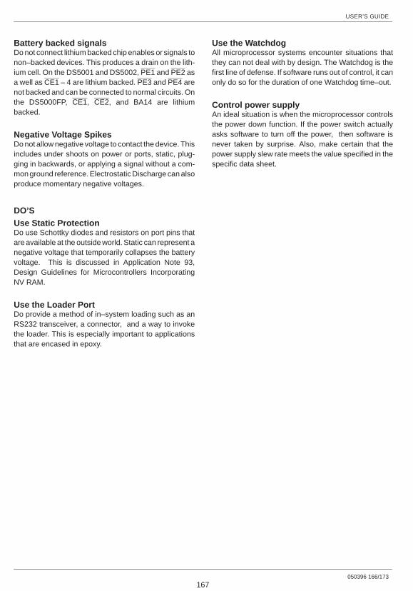
USER’S GUIDE
050396 166/173
167
Battery backed signalsDo not connect lithium backed chip enables or signals tonon–backed devices. This produces a drain on the lith-ium cell. On the DS5001 and DS5002, PE1 and PE2 asa well as CE1 – 4 are lithium backed. PE3 and PE4 arenot backed and can be connected to normal circuits. Onthe DS5000FP, CE1, CE2, and BA14 are lithiumbacked.
Negative Voltage SpikesDo not allow negative voltage to contact the device. Thisincludes under shoots on power or ports, static, plug-ging in backwards, or applying a signal without a com-mon ground reference. Electrostatic Discharge can alsoproduce momentary negative voltages.
DO’SUse Static ProtectionDo use Schottky diodes and resistors on port pins thatare available at the outside world. Static can represent anegative voltage that temporarily collapses the batteryvoltage. This is discussed in Application Note 93,Design Guidelines for Microcontrollers IncorporatingNV RAM.
Use the Loader PortDo provide a method of in–system loading such as anRS232 transceiver, a connector, and a way to invokethe loader. This is especially important to applicationsthat are encased in epoxy.
Use the WatchdogAll microprocessor systems encounter situations thatthey can not deal with by design. The Watchdog is thefirst line of defense. If software runs out of control, it canonly do so for the duration of one Watchdog time–out.
Control power supplyAn ideal situation is when the microprocessor controlsthe power down function. If the power switch actuallyasks software to turn off the power, then software isnever taken by surprise. Also, make certain that thepower supply slew rate meets the value specified in thespecific data sheet.
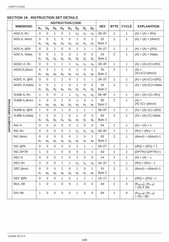
USER’S GUIDE
050396 167/173
168
SECTION 19: INSTRUCTION SET DETAILS
MNEMONICINSTRUCTION CODE
HEX BYTE CYCLE EXPLANATIONMNEMONIC D7 D6 D5 D4 D3 D2 D1 D0HEX BYTE CYCLE EXPLANATION
ADD A, Rn 0 0 1 0 1 n2 n1 n0 28–2F 1 1 (A) = (A) + (Rn)
ADD A, direct 0a7
0a6
1a5
0a4
0a3
1a2
0a1
1a0
25Byte 2
2 1 (A) = (A) + (direct)
ADD A, @Ri 0 0 1 0 0 1 1 i 26–27 1 1 (A) = (A) + ((Ri))
ADD A, #data 0d7
0d6
1d5
0d4
0d3
1d2
0d1
0d0
24Byte 2
2 1 (A) = (A) + #data
ADDC A, Rn 0 0 1 1 1 n2 n1 n0 38–3F 1 1 (A) = (A)+(C)+(Rn)
ADDCA,direct 0a7
0a6
1a5
1a4
0a3
1a2
0a1
1a0
35Byte 2
2 1 (A) =(A)+(C)+(direct)
ADDC A, @Ri 0 0 1 1 0 1 1 i 36–37 1 1 (A) = (A)+(C)+((Ri))
ADDC A,#data 0d7
0d6
1d5
1d4
0d3
1d2
0d1
0d0
34Byte 2
2 1 (A) = (A)+(C)+#data
SUBB A, Rn 1 0 0 1 1 n2 n1 n0 98–9F 1 1 (A) = (A)–(C)–(Rn)
AT
ION SUBB A,direct 1
a7
0a6
0a5
1a4
0a3
1a2
0a1
1a0
95Byte 2
2 1 (A) = (A)–(C)–(direct)
PE
RA
SUBB A, @Ri 1 0 0 1 0 1 1 i 96–97 1 1 (A) = (A)–(C)–((Ri))
ME
TIC
OP
SUBB A,#data 1d7
0d6
0d5
1d4
0d3
1d2
0d1
0d0
94Byte 2
2 1 (A) = (A)-(C)-#data
ITH
M
INC A 0 0 0 0 0 1 0 0 04 1 1 (A) = (A) + 1
AR
IT
INC Rn 0 0 0 0 1 n2 n1 n0 08–0F 1 1 (Rn) = (Rn) + 1
INC direct 0a7
0a6
0a5
0a4
0a3
1a2
0a1
1a0
05Byte 2
2 1 (direct) = (direct)+1
INC @Ri 0 0 0 0 0 1 1 i 06–07 1 1 ((Ri)) = ((Ri)) + 1
INC DPTR 1 0 1 0 0 0 1 1 A3 1 2 (DPTR)=(DPTR)+1
DEC A 0 0 0 1 0 1 0 0 14 1 1 (A) = (A) – 1
DEC Rn 0 0 0 1 1 n2 n1 n0 18–1F 1 1 (Rn) = (Rn) – 1
DEC direct 0a7
0a6
0a5
1a4
0a3
1a2
0a1
1a0
15Byte 2
2 1 (direct) = (direct)–1
DEC @Ri 0 0 0 1 0 1 1 i 16–17 1 1 ((Ri)) = ((Ri)) –1
MUL AB 1 0 1 0 0 1 0 0 A4 1 4 (B15–8), (A7–0)= (A) X (B)
DIV AB 1 0 0 0 0 1 0 0 84 1 4 (A15–8), (A7–0)= (A)�(B)
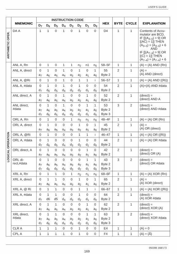
USER’S GUIDE
050396 168/173
169
EXPLANATIONCYCLEBYTEHEXINSTRUCTION CODE
MNEMONIC EXPLANATIONCYCLEBYTEHEXD0D1D2D3D4D5D6D7MNEMONIC
AR
ITH
ME
TIC
OP
ER
. DA A 1 1 0 1 0 1 0 0 D4 1 1 Contents of Accu-mulator are BCD, IF [[(A3–0) > 9] OR[(AC) = 1]] THEN(A3–0) = (A3–0) + 6
AND IF [[(A7–4) > 9] OR[(C) = 1]] THEN(A7–4) = (A7–4) + 6
ANL A, Rn 0 1 0 1 1 n2 n1 n0 58–5F 1 1 (A) = (A) AND (Rn)
ANL A, direct 0a7
1a6
0a5
1a4
0a3
1a2
0a1
1a0
55Byte 2
2 1 (A) =(A) AND (direct)
ANL A, @Ri 0 1 0 1 0 1 1 i 56–57 1 1 (A) = (A) AND ((Ri))
ANL A, #data 0d7
1d6
0d5
1d4
0d3
1d2
0d1
0d0
54Byte 2
2 1 (A)=(A) AND #data
ANL direct, A 0a7
1a6
0a5
1a4
0a3
0a2
1a1
0a0
52Byte 2
2 1 (direct) =(direct) AND A
ANL direct,#data
0a7d7
1a6d6
0a5d5
1a4d4
0a3d3
0a2d2
1a1d1
1a0d0
53Byte 2Byte 3
3 2 (direct) =(direct) AND #data
ORL A, Rn 0 1 0 0 1 n2 n1 n0 48–4F 1 1 (A) = (A) OR (Rn)
ORL A, direct 0a7
1a6
0a5
0a4
0a3
1a2
0a1
1a0
45Byte 2
2 1 (A) =(A) OR (direct)
TIO
N ORL A, @Ri 0 1 0 0 0 1 1 i 46–47 1 1 (A) = (A) OR ((Ri))
OP
ER
AT ORL A, #data 0d7
1d6
0d5
0d4
0d3
1d2
0d1
0d0
44Byte 2
2 1 (A) = (A) OR #data
GIC
AL
O
ORL direct, A 0a7
1a6
0a5
0a4
0a3
0a2
1a1
0a0
42Byte 2
2 1 (direct) =(direct) OR (A)
LOG
ORL di-rect,#data
0a7d7
1a6d6
0a5d5
0a4d4
0a3d3
0a2d2
1a1d1
1a0d0
43Byte 2Byte 3
3 2 (direct) = (direct) OR #data
XRL A, Rn 0 1 1 0 1 n2 n1 n0 68–6F 1 1 (A) = (A) XOR (Rn)
XRL A, direct 0a7
1a6
1a5
0a4
0a3
1a2
0a1
1a0
65Byte 2
2 1 (A) = (A) XOR (direct)
XRL A, @ Ri 0 1 1 0 0 1 1 i 66–67 1 1 (A) = (A) XOR ((Ri))
XRL A, #data 0d7
1d6
1d5
0d4
0d3
1d2
0d1
0d0
64Byte 2
2 1 (direct) =(A) XOR #data
XRL direct, A 0a7
1a6
1a5
0a4
0a3
0a2
1a1
0a0
62Byte 2
2 1 (direct) =(direct) XOR (A)
XRL direct,#data
0a7d7
1a6d6
1a5d5
0a4d4
0a3d3
0a2d2
1a1d1
1a0d0
63Byte 2Byte 3
3 2 (direct) =(direct) XOR #data
CLR A 1 1 1 0 0 1 0 0 E4 1 1 (A) = 0
CPL A 1 1 1 1 0 1 0 0 F4 1 1 (A) = (A)

USER’S GUIDE
050396 169/173
170
EXPLANATIONCYCLEBYTEHEXINSTRUCTION CODE
MNEMONIC EXPLANATIONCYCLEBYTEHEXD0D1D2D3D4D5D6D7MNEMONIC
RL A 0 0 1 0 0 0 1 1 23 1 1A1A7 A6 A5 A4 A3 A2 A0
The contents of theaccumulator are ro-tated left by one bit.
RAT
ION
RLC A 0 0 1 1 0 0 1 1 33 1 1A1A7 A6 A5 A4 A3 A2 A0
The contents of theaccumulator are ro-tated left by one bit.
C
LOG
ICA
L O
PE
R
RR A 0 0 0 0 0 0 1 1 03 1 1
The contents ofthe accumulatorare rotated rightby one bit.
A1A7 A6 A5 A4 A3 A2 A0
RRC A 0 0 0 1 0 0 1 1 13 1 1A1A7 A6 A5 A4 A3 A2 A0
The contents of theaccumulator are ro-tated right by onebit.
C
SWAP A 1 1 0 0 0 1 0 0 C4 1 1 (A3–0) � (A7–4)
MOV A, Rn 1 1 1 0 1 n2 n1 n0 E8–EF 1 1 (A) = (Rn)
MOV A, direct 1a7
1a6
1a3
0a4
0a3
1a2
0a1
1a0
E5Byte 2
2 1 (A) = (direct)
MOV A, @Ri 1 1 1 0 0 1 1 i E6–E7 1 1 (A) = ((Ri))
MOV A, #data 0d7
1d6
1d5
1d4
0d3
1d2
0d1
0d0
74Byte 2
2 1 (A) = #data
MOV Rn, A 1 1 1 1 1 n2 n1 n0 F8–FF 1 1 (Rn) = (A)
NS
FE
R MOV Rn, direct
1a7
0a6
1a5
0a4
1a3
n2a2
n1a1
n0a0
A8–AFByte 2
2 2 (Rn) = (direct)
TA T
RA
N
MOV Rn,#data
0d7
1d6
1d5
1d4
1d3
n2d2
n1d1
n0d0
78–7FByte 2
2 1 (Rn) = #data
DA
T
MOV direct, A 1a7
1a6
1a5
1a4
0a3
1a2
0a1
1a0
F5Byte 2
2 1 (direct) = (A)
MOV direct,Rn
1a7
0a6
0a5
0a4
1a3
n2a2
n1a1
n0a0
88–8FByte 2
2 2 (direct) = (Rn)
MOV direct1,direct2
1a7a7
0a6a6
0a5a5
0a4a4
0a3a3
1a2a2
0a1a1
1a0a0
85Byte 2Byte 3
3 2 (direct1) = (direct2)(source) (destination)
MOV direct,@Ri
1a7
0a6
0a5
0a4
0a3
1a2
1a1
ia0
86–87Byte 2
2 2 (direct) = ((Ri))
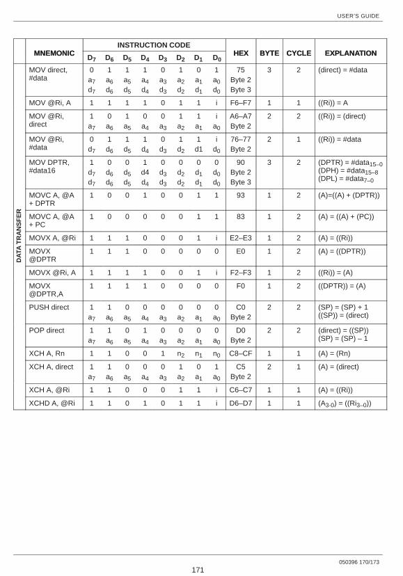
USER’S GUIDE
050396 170/173
171
EXPLANATIONCYCLEBYTEHEXINSTRUCTION CODE
MNEMONIC EXPLANATIONCYCLEBYTEHEXD0D1D2D3D4D5D6D7MNEMONIC
MOV direct,#data
0a7d7
1a6d6
1a5d5
1a4d4
0a3d3
1a2d2
0a1d1
1a0d0
75Byte 2Byte 3
3 2 (direct) = #data
MOV @Ri, A 1 1 1 1 0 1 1 i F6–F7 1 1 ((Ri)) = A
MOV @Ri, direct
1a7
0a6
1a5
0a4
0a3
1a2
1a1
ia0
A6–A7Byte 2
2 2 ((Ri)) = (direct)
MOV @Ri,#data
0d7
1d6
1d5
1d4
0d3
1d2
1d1
id0
76–77Byte 2
2 1 ((Ri)) = #data
MOV DPTR,#data16
1d7d7
0d6d6
0d5d5
1d4d4
0d3d3
0d2d2
0d1d1
0d0d0
90Byte 2Byte 3
3 2 (DPTR) = #data15–0(DPH) = #data15–8(DPL) = #data7–0
R
MOVC A, @A+ DPTR
1 0 0 1 0 0 1 1 93 1 2 (A)=((A) + (DPTR))
AN
SF
ER
MOVC A, @A+ PC
1 0 0 0 0 0 1 1 83 1 2 (A) = ((A) + (PC))
TR
AN
MOVX A, @Ri 1 1 1 0 0 0 1 i E2–E3 1 2 (A) = ((Ri))
DAT
A T
MOVX@DPTR
1 1 1 0 0 0 0 0 E0 1 2 (A) = ((DPTR))
MOVX @Ri, A 1 1 1 1 0 0 1 i F2–F3 1 2 ((Ri)) = (A)
MOVX@DPTR,A
1 1 1 1 0 0 0 0 F0 1 2 ((DPTR)) = (A)
PUSH direct 1a7
1a6
0a5
0a4
0a3
0a2
0a1
0a0
C0Byte 2
2 2 (SP) = (SP) + 1((SP)) = (direct)
POP direct 1a7
1a6
0a5
1a4
0a3
0a2
0a1
0a0
D0Byte 2
2 2 (direct) = ((SP))(SP) = (SP) – 1
XCH A, Rn 1 1 0 0 1 n2 n1 n0 C8–CF 1 1 (A) = (Rn)
XCH A, direct 1a7
1a6
0a5
0a4
0a3
1a2
0a1
1a0
C5Byte 2
2 1 (A) = (direct)
XCH A, @Ri 1 1 0 0 0 1 1 i C6–C7 1 1 (A) = ((Ri))
XCHD A, @Ri 1 1 0 1 0 1 1 i D6–D7 1 1 (A3-0) = ((Ri3–0))
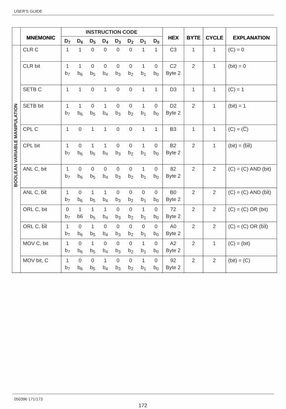
USER’S GUIDE
050396 171/173
172
EXPLANATIONCYCLEBYTEHEXINSTRUCTION CODE
MNEMONIC EXPLANATIONCYCLEBYTEHEXD0D1D2D3D4D5D6D7MNEMONIC
CLR C 1 1 0 0 0 0 1 1 C3 1 1 (C) = 0
CLR bit 1b7
1b6
0b5
0b4
0b3
0b2
1b1
0b0
C2Byte 2
2 1 (bit) = 0
SETB C 1 1 0 1 0 0 1 1 D3 1 1 (C) = 1
PU
LAT
ION SETB bit 1
b7
1b6
0b5
1b4
0b3
0b2
1b1
0b0
D2Byte 2
2 1 (bit) = 1
E M
AN
IP CPL C 1 0 1 1 0 0 1 1 B3 1 1 (C) = (C)
N V
AR
IAB
LE
CPL bit 1b7
0b6
1b5
1b4
0b3
0b2
1b1
0b0
B2Byte 2
2 1 (bit) = (bit)
BO
OLE
AN
ANL C, bit 1b7
0b6
0b5
0b4
0b3
0b2
1b1
0b0
82Byte 2
2 2 (C) = (C) AND (bit)
ANL C, bit 1b7
0b6
1b5
1b4
0b3
0b2
0b1
0b0
B0Byte 2
2 2 (C) = (C) AND (bit)
ORL C, bit 0b7
1b6
1b5
1b4
0b3
0b2
1b1
0b0
72Byte 2
2 2 (C) = (C) OR (bit)
ORL C, bit 1b7
0b6
1b5
0b4
0b3
0b2
0b1
0b0
A0Byte 2
2 2 (C) = (C) OR (bit)
MOV C, bit 1b7
0b6
1b5
0b4
0b3
0b2
1b1
0b0
A2Byte 2
2 1 (C) = (bit)
MOV bit, C 1b7
0b6
0b5
1b4
0b3
0b2
1b1
0b0
92Byte 2
2 2 (bit) = (C)
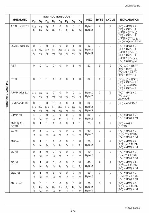
USER’S GUIDE
050396 172/173
173
EXPLANATIONCYCLEBYTEHEXINSTRUCTION CODE
MNEMONIC EXPLANATIONCYCLEBYTEHEXD0D1D2D3D4D5D6D7MNEMONIC
ACALL addr 11 a10a7
a9a6
a8a5
1a4
0a3
0a2
0a1
1a0
Byte 1Byte 2
2 2 (PC) = (PC) + 2(SP) = (SP) + 1((SP)) = (PC7–0)(SP) = (SP) + 1((SP)) = (PC15–8)(PC)=page address
LCALL addr 16 0a15a7
0a14a6
0a13a5
1a12a4
0a11a3
0a10a2
1a9a1
0a8a0
12Byte 2Byte 3
3 2 (PC) = (PC) + 3(SP) = (SP) + 1((SP)) = (PC7–0)(SP) = (SP) + 1((SP)) = (PC15–8)(PC) = addr15–0
RET 0 0 1 0 0 0 1 0 22 1 2 (PC15–8) = ((SP))(SP) = (SP) – 1(PC7–0) = ((SP))(SP) = (SP) – 1
AN
CH
ING
RETI 0 0 1 1 0 0 1 0 32 1 2 (PC15–8) = ((SP))(SP) = (SP) – 1(PC7-0) = ((SP))(SP) = (SP) – 1
RA
M B
RA
N
AJMP addr 11 a10a7
a9a6
a8a5
0a4
0a3
0a2
0a1
1a0
Byte 1Byte 2
2 2 (PC) = (PC) + 2(PC10-0) = page addr
PR
OG
R
LJMP addr 16 0a15a7
0a14a6
0a13a5
0a12a4
0a11a3
0a10a2
1a9a1
0a8a0
02Byte 2Byte 3
3 2 (PC) = addr15-0
SJMP rel 1r7
0r6
0r5
0r4
0r3
0r2
0r1
0r0
80Byte 2
2 2 (PC) = (PC) + 2(PC) = (PC) + rel
JMP @A +DPTR
0 1 1 1 0 0 1 1 73 1 2 (PC) = (A) +(DPTR)
JZ rel 0r7
1r6
1r5
0r4
0r3
0r2
0r1
0r0
60Byte 2
2 2 (PC) = (PC) + 2 IF (A) = 0 THEN(PC) = (PC) + rel
JNZ rel 0r7
1r6
1r5
1r4
0r3
0r2
0r1
0r0
70Byte 2
2 2 (PC) = (PC) + 2IF (A) � 0 THEN(PC) = (PC) + rel
JC rel 0r7
1r6
0r5
0r4
0r3
0r2
0r1
0r0
40Byte 2
2 2 (PC) = (PC) + 2IF (C) = 1 THEN(PC) = (PC) + rel
JC rel 0r7
1r6
0r5
0r4
0r3
0r2
0r1
0r0
40Byte 2
2 2 (PC) = (PC) + 2IF (C) = 1 THEN(PC) = (PC) + rel
JNC rel 0r7
1r6
0r5
1r4
0r3
0r2
0r1
0r0
50Byte 2
2 2 (PC) = (PC) + 2IF (C) � 0 THEN(PC) = (PC) + rel
JB bit, rel 0b7r7
0b6r6
1b5r5
0b4r4
0b3r3
0b2r2
0b1r1
0b0r0
20Byte 2Byte 3
3 2 (PC) = (PC) + 3IF (bit) = 1 THEN(PC) = (PC) + rel

USER’S GUIDE
050396 173/173
174
EXPLANATIONCYCLEBYTEHEXINSTRUCTION CODE
MNEMONIC EXPLANATIONCYCLEBYTEHEXD0D1D2D3D4D5D6D7MNEMONIC
JNB bit, rel 0b7r7
0b6r6
1b5r5
1b4r4
0b3r3
0b2r2
0b1r1
0b0r0
30Byte 2Byte 3
3 2 (PC) = (PC) + 3IF (bit) = 0 THEN(PC) = (PC) + rel
JBC bit, directrel
0b7r7
0b6r6
0b5r5
1b4r4
0b3r3
0b2r2
0b1r1
0b0r0
10Byte 2Byte 3
3 2 (PC) = (PC) + 3IF (bit) = 1 THEN(bit) = 0 (PC) =(PC) + rel
CJNE A, directrel
1
a7r7
0
a6r6
1
a5r5
1
adr4
0
a3r3
1
a2r2
0
a1r1
1
a0r0
B5Byte 2Byte 3
3 2 (PC) = (PC) + 3IF (direct) < (A)THEN (PC) = (PC)+ rel and (C) = 0
ORIF (direct) > (A)THEN (PC) = (PC)+ rel and (C) = 1
RO
GR
AM
BR
AN
CH
ING CJNE A, #data
rel1
d7r7
0
d6r6
1
d5r5
1
d4r4
0
d3r3
1
d2r2
0
d1r1
0
d0r0
B4Byte 2Byte 3
3 2 (PC) = (PC) + 3IF #data < (A)THEN (PC) = (PC)+ rel and (C) = 0
ORIF #data > (A)THEN (PC) = (PC)+ rel and (C) = 1
PR
CJNE Rn,#data rel
1
d7r7
0
d6r6
1
d5r5
1
d4r4
1
d3r3
n2
d2r2
n1
d1r1
n0
d0r0
B8-BFByte 2Byte 3
3 2 (PC) = (PC) + 3IF #data < (Rn)THEN (PC) = (PC)+ rel and (C) = 0
ORIF #data > (Rn)THEN (PC) = (PC)+ rel and (C) = 1
CJNE @Ri,#data rel
1
d7r7
0
d6r6
1
d5r5
1
d4r4
0
d3r3
1
d2r2
1
d1r1
i
d0r0
B6-B7Byte 2Byte 3
3 2 (PC) = (PC) + 3IF #data < ((Ri))THEN (PC) = (PC)+ rel and (C) = 0
ORIF #data > ((Ri))THEN (PC) = (PC)+ rel and (C) = 1
DJNZ Rn, rel 1r7
1r6
0r5
1r4
1r3
n2r2
n1r1
n0r0
D8-DfByte 2
2 2 (PC) = (PC) + 2(Rn) = (Rn) – 1 IF (Rn) 0 THEN(PC) = (PC) + rel
DJNZ direct rel 1a7r7
1a6r6
0a5r5
1a4r4
0a3r3
1a2r2
0a1r1
1a0r0
D5Byte 2Byte 3
3 2 (PC) = (PC) + 3(direct) = (direct)–1IF (direct)�0 THEN(PC) = (PC) + rel
NOP 0 0 0 0 0 0 0 0 00 1 1 (PC) = (PC) + 1