mb96610 series f2mc-16fx,16-bit proprietary microcontroller · mb96610 series f2mc-16fx,16-bit...
TRANSCRIPT
MB96610 Series
F2MC-16FX,16-bit Proprietary Microcontroller
Cypress Semiconductor Corporation • 198 Champion Court • San Jose, CA 95134-1709 • 408-943-2600 Document Number: 002-04709 Rev.*C Revised July 11, 2017
MB96610 series is based on Cypress advanced F2MC-16FX architecture (16-bit with instruction pipeline for RISC-like
performance). The CPU uses the same instruction set as the established F2MC-16LX family thus allowing for easy
migration of F2MC-16LX Software to the new F2MC-16FX products. F2MC-16FX product improvements compared to
the previous generation include significantly improved performance - even at the same operation frequency, reduced
power consumption and faster start-up time.For high processing speed at optimized power consumption an internal
PLL can be selected to supply the CPU with up to 32MHz operation frequency from an external 4MHz to 8MHz resonator.
The result is a minimum instruction cycle time of 31.2ns going together with excellent EMI behavior. The emitted power
is minimized by the on-chip voltage regulator that reduces the internal CPU voltage. A flexible clock tree allows selecting
suitable operation frequencies for peripheral resources independent of the CPU speed.
Features
Technology
0.18µm CMOS
CPU
F2MC-16FX CPU
Optimized instruction set for controller applications (bit, byte, word and long-word data types, 23 different addressing modes, barrel shift, variety of pointers)
8-byte instruction queue
Signed multiply (16-bit 16-bit) and divide (32-bit/16-bit) instructions available
System clock
On-chip PLL clock multiplier (1 to 8, 1 when PLL stop)
4MHz to 8MHz crystal oscillator (maximum frequency when using ceramic resonator depends on Q-factor)
Up to 8MHz external clock for devices with fast clock input feature
32.768kHz subsystem quartz clock
100kHz/2MHz internal RC clock for quick and safe startup, clock stop detection function, watchdog
Clock source selectable from mainclock oscillator, subclock oscillator and on-chip RC oscillator, independently for CPU and 2 clock domains of peripherals
The subclock oscillator is enabled by the Boot ROM program controlled by a configuration marker after a Power or External reset
Low Power Consumption - 13 operating modes (different Run, Sleep, Timer, Stop modes)
On-chip voltage regulator
Internal voltage regulator supports a wide MCU supply voltage range (Min=2.7V), offering low power consumption
Low voltage detection function
Reset is generated when supply voltage falls below programmable reference voltage
Code Security
Protects Flash Memory content from unintended read-out
DMA
Automatic transfer function independent of CPU, can be assigned freely to resources
Interrupts
Fast Interrupt processing
8 programmable priority levels
Non-Maskable Interrupt (NMI)
CAN
Supports CAN protocol version 2.0 part A and B
ISO16845 certified
Bit rates up to 1Mbps
32 message objects
Each message object has its own identifier mask
Programmable FIFO mode (concatenation of message objects)
Maskable interrupt
Disabled Automatic Retransmission mode for Time Triggered CAN applications
Programmable loop-back mode for self-test operation
USART
Full duplex USARTs (SCI/LIN)
Wide range of baud rate settings using a dedicated reload timer
Special synchronous options for adapting to different synchronous serial protocols
Document Number: 002-04709 Rev.*C Page 2 of 63
MB96610 Series
LIN functionality working either as master or slave LIN device
Extended support for LIN-Protocol to reduce interrupt load
A/D converter
SAR-type
8/10-bit resolution
Signals interrupt on conversion end, single conversion mode, continuous conversion mode, stop conversion mode, activation by software, external trigger, reload timers and PPGs
Range Comparator Function
Source Clock Timers
Three independent clock timers (23-bit RC clock timer, 23-bit Main clock timer, 17-bit Sub clock timer)
Hardware Watchdog Timer
Hardware watchdog timer is active after reset
Window function of Watchdog Timer is used to select the lower window limit of the watchdog interval
Reload Timers
16-bit wide
Prescaler with 1/21, 1/22, 1/23, 1/24, 1/25, 1/26 of peripheral clock frequency
Event count function
Free-Running Timers
Signals an interrupt on overflow, supports timer clear upon match with Output Compare (0, 4)
Prescaler with 1, 1/21, 1/22, 1/23, 1/24, 1/25, 1/26, 1/27, 1/28 of peripheral clock frequency
Input Capture Units
16-bit wide
Signals an interrupt upon external event
Rising edge, Falling edge or Both (rising & falling) edges sensitive
Output Compare Units
16-bit wide
Signals an interrupt when a match with Free-running Timer occurs
A pair of compare registers can be used to generate an output signal
Programmable Pulse Generator
16-bit down counter, cycle and duty setting registers
Can be used as 2 ×8-bit PPG
Interrupt at trigger, counter borrow and/or duty match
PWM operation and one-shot operation
Internal prescaler allows 1, 1/4, 1/16, 1/64 of peripheral clock as counter clock or of selected Reload timer underflow as clock input
Can be triggered by software or reload timer
Can trigger ADC conversion
Timing point capture
Quadrature Position/Revolution Counter (QPRC)
Up/down count mode, Phase difference count mode, Count mode with direction
16-bit position counter
16-bit revolution counter
Two 16-bit compare registers with interrupt
Detection edge of the three external event input pins AIN, BIN and ZIN is configurable
Real Time Clock
Operational on main oscillation (4MHz), sub oscillation (32kHz) or RC oscillation (100kHz/2MHz)
Capable to correct oscillation deviation of Sub clock or RC oscillator clock (clock calibration)
Read/write accessible second/minute/hour registers
Can signal interrupts every half second/second/minute/hour/day
Internal clock divider and prescaler provide exact 1s clock
External Interrupts
Edge or Level sensitive
Interrupt mask bit per channel
Each available CAN channel RX has an external interrupt for wake-up
Selected USART channels SIN have an external interrupt for wake-up
Non Maskable Interrupt
Disabled after reset, can be enabled by Boot-ROM depending on ROM configuration block
Once enabled, can not be disabled other than by reset
High or Low level sensitive
Pin shared with external interrupt 0
I/O Ports
Most of the external pins can be used as general purpose I/O
All push-pull outputs
Bit-wise programmable as input/output or peripheral signal
Bit-wise programmable input enable
One input level per GPIO-pin (either Automotive or CMOS hysteresis)
Bit-wise programmable pull-up resistor
Document Number: 002-04709 Rev.*C Page 3 of 63
MB96610 Series
Built-in On Chip Debugger (OCD)
One-wire debug tool interface
Break function:
Hardware break: 6 points (shared with code event)
Software break: 4096 points
Event function
Code event: 6 points (shared with hardware break)
Data event: 6 points
Event sequencer: 2 levels + reset
Execution time measurement function
Trace function: 42 branches
Security function
Flash Memory
Dual operation flash allowing reading of one Flash bank while programming or erasing the other bank
Command sequencer for automatic execution of programming algorithm and for supporting DMA for programming of the Flash Memory
Supports automatic programming, Embedded Algorithm
Write/Erase/Erase-Suspend/Resume commands
A flag indicating completion of the automatic algorithm
Erase can be performed on each sector individually
Sector protection
Flash Security feature to protect the content of the Flash
Low voltage detection during Flash erase or write
Document Number: 002-04709 Rev.*C Page 4 of 63
MB96610 Series
Contents
1. Product Lineup .................................................................................................................................................... 6 2. Block Diagram ..................................................................................................................................................... 7 3. Pin Assignment ................................................................................................................................................... 8 4. Pin Description .................................................................................................................................................... 9 5. Pin Circuit Type ................................................................................................................................................. 11 6. I/O Circuit Type .................................................................................................................................................. 13 7. Memory Map ...................................................................................................................................................... 18 8. RAMstart Addresses ......................................................................................................................................... 19 9. User ROM Memory Map for Flash Devices ..................................................................................................... 20 10. Serial Programming Communication Interface .............................................................................................. 21 11. Interrupt Vector Table ....................................................................................................................................... 22 12. Handling Precautions ....................................................................................................................................... 26 12.1 Precautions for Product Design ........................................................................................................................ 26 12.2 Precautions for Package Mounting ................................................................................................................... 27 12.3 Precautions for Use Environment ..................................................................................................................... 29 13. Handling Devices .............................................................................................................................................. 30 13.1 Latch-up prevention .......................................................................................................................................... 30 13.2 Unused pins handling ....................................................................................................................................... 30 13.3 External clock usage ........................................................................................................................................ 30 13.3.1 Single phase external clock for Main oscillator.................................................................................................. 30 13.3.2 Single phase external clock for Sub oscillator ................................................................................................... 31 13.3.3 Opposite phase external clock .......................................................................................................................... 31 13.4 Notes on PLL clock mode operation ................................................................................................................. 31 13.5 Power supply pins (Vcc/Vss) ............................................................................................................................ 31 13.6 Crystal oscillator and ceramic resonator circuit ................................................................................................ 31 13.7 Turn on sequence of power supply to A/D converter and analog inputs........................................................... 32 13.8 Pin handling when not using the A/D converter ................................................................................................ 32 13.9 Notes on Power-on ........................................................................................................................................... 32 13.10 Stabilization of power supply voltage................................................................................................................ 32 13.11 Serial communication ....................................................................................................................................... 32 13.12 Mode Pin (MD) ................................................................................................................................................. 32 14. Electrical Characteristics ................................................................................................................................. 33 14.1 Absolute Maximum Ratings .............................................................................................................................. 33 14.2 Recommended Operating Conditions............................................................................................................... 35 14.3 DC Characteristics............................................................................................................................................ 36 14.3.1 Current Rating ................................................................................................................................................... 36 14.3.2 Pin Characteristics ............................................................................................................................................ 39 14.4 AC Characteristics ............................................................................................................................................ 40 14.4.1 Main Clock Input Characteristics ....................................................................................................................... 40 14.4.2 Sub Clock Input Characteristics ........................................................................................................................ 41 14.4.3 Built-in RC Oscillation Characteristics ............................................................................................................... 42 14.4.4 Internal Clock Timing ........................................................................................................................................ 42 14.4.5 Operating Conditions of PLL ............................................................................................................................. 43 14.4.6 Reset Input ........................................................................................................................................................ 43 14.4.7 Power-on Reset Timing ..................................................................................................................................... 44 14.4.8 USART Timing .................................................................................................................................................. 45 14.4.9 External Input Timing ........................................................................................................................................ 47 14.5 A/D Converter ................................................................................................................................................... 48 14.5.1 Electrical Characteristics for the A/D Converter ................................................................................................ 48
Document Number: 002-04709 Rev.*C Page 5 of 63
MB96610 Series
14.5.2 Accuracy and Setting of the A/D Converter Sampling Time .............................................................................. 49 14.5.3 Definition of A/D Converter Terms .................................................................................................................... 49 14.6 Low Voltage Detection Function Characteristics .............................................................................................. 52 14.7 Flash Memory Write/Erase Characteristics ...................................................................................................... 54 15. Example Characteristics ................................................................................................................................... 55 16. Ordering Information ........................................................................................................................................ 58 17. Package Dimension .......................................................................................................................................... 59 18. Major Changes .................................................................................................................................................. 60 Document History ...................................................................................................................................................... 62
Document Number: 002-04709 Rev.*C Page 6 of 63
MB96610 Series
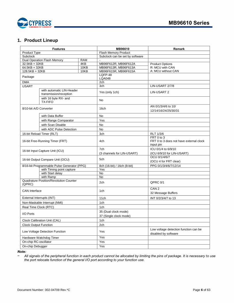
1. Product Lineup
Features MB96610 Remark
Product Type Flash Memory Product
Subclock Subclock can be set by software
Dual Operation Flash Memory RAM -
32.5KB + 32KB 4KB MB96F612R, MB96F612A Product Options R: MCU with CAN A: MCU without CAN
64.5KB + 32KB 10KB MB96F613R, MB96F613A
128.5KB + 32KB 10KB MB96F615R, MB96F615A
Package LQFP-48 LQA048
DMA 2ch
USART 3ch LIN-USART 2/7/8
with automatic LIN-Header transmission/reception
Yes (only 1ch) LIN-USART 2
with 16 byte RX- and TX-FIFO
No
8/10-bit A/D Converter 16ch AN 0/1/3/4/6 to 10/
12/14/16/24/25/30/31
with Data Buffer No
with Range Comparator Yes
with Scan Disable No
with ADC Pulse Detection No
16-bit Reload Timer (RLT) 3ch RLT 1/3/6
16-bit Free-Running Timer (FRT) 4ch FRT 0 to 3 FRT 0 to 3 does not have external clock input pin
16-bit Input Capture Unit (ICU) 7ch
(3 channels for LIN-USART)
ICU 0/1/4 to 6/9/10
(ICU 6/9/10 for LIN-USART)
16-bit Output Compare Unit (OCU) 5ch OCU 0/1/4/6/7
(OCU 4 for FRT clear)
8/16-bit Programmable Pulse Generator (PPG) 8ch (16-bit) / 16ch (8-bit) PPG 0/1/3/4/6/7/12/14
with Timing point capture Yes
with Start delay No
with Ramp No
Quadrature Position/Revolution Counter (QPRC)
2ch QPRC 0/1
CAN Interface 1ch CAN 2
32 Message Buffers
External Interrupts (INT) 11ch INT 0/2/3/4/7 to 13
Non-Maskable Interrupt (NMI) 1ch
Real Time Clock (RTC) 1ch
I/O Ports 35 (Dual clock mode)
37 (Single clock mode)
Clock Calibration Unit (CAL) 1ch
Clock Output Function 2ch
Low Voltage Detection Function Yes Low voltage detection function can be
disabled by software
Hardware Watchdog Timer Yes
On-chip RC-oscillator Yes
On-chip Debugger Yes
Note:
− All signals of the peripheral function in each product cannot be allocated by limiting the pins of package. It is necessary to use the port relocate function of the general I/O port according to your function use.
Document Number: 002-04709 Rev.*C Page 7 of 63
MB96610 Series
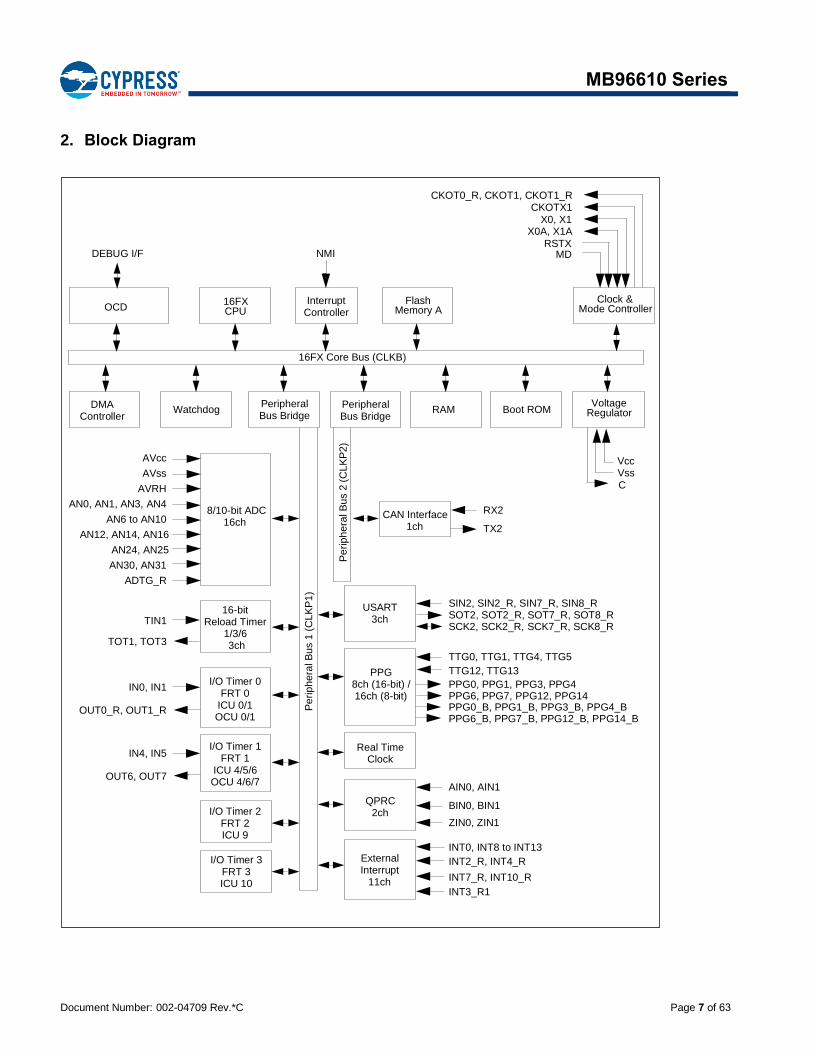
2. Block Diagram
MD
InterruptController
DMAController
Pe
rip
he
ral B
us 1
(CL
KP
1)
Pe
rip
he
ral B
us 2
(CL
KP
2)
I/O Timer 3FRT 3ICU 10
I/O Timer 2FRT 2ICU 9
I/O Timer 1FRT 1
ICU 4/5/6OCU 4/6/7
I/O Timer 0FRT 0
ICU 0/1OCU 0/1
16-bitReload Timer
1/3/6
8/10-bit ADC16ch
CAN Interface1ch
USART3ch
PPG8ch (16-bit) /16ch (8-bit)
Real TimeClock
ExternalInterrupt
11ch
QPRC2ch
VccVss
PPG0, PPG1, PPG3, PPG4
OUT0_R, OUT1_R
IN0, IN1
C
PeripheralBus Bridge
PeripheralBus Bridge
16FX Core Bus (CLKB)
TIN1
TOT1, TOT3
AVcc
AVss
AVRH
AN12, AN14, AN16
ADTG_R
AN6 to AN10
IN4, IN5
OUT6, OUT7
INT2_R, INT4_R
INT7_R, INT10_R
AN24, AN25
AN30, AN31
RAM Boot ROMWatchdogVoltage
Regulator
SIN2, SIN2_R, SIN7_R, SIN8_RSOT2, SOT2_R, SOT7_R, SOT8_RSCK2, SCK2_R, SCK7_R, SCK8_R
TX2
RX2
16FXCPU
Clock &Mode Controller
FlashMemory A
NMI
AIN0, AIN1
BIN0, BIN1
ZIN0, ZIN1
TTG0, TTG1, TTG4, TTG5
CKOT0_R, CKOT1, CKOT1_RCKOTX1
X0, X1X0A, X1A
RSTX
PPG6, PPG7, PPG12, PPG14PPG0_B, PPG1_B, PPG3_B, PPG4_BPPG6_B, PPG7_B, PPG12_B, PPG14_B
TTG12, TTG13
INT0, INT8 to INT13
INT3_R1
OCD
DEBUG I/F
AN0, AN1, AN3, AN4
3ch
Document Number: 002-04709 Rev.*C Page 8 of 63
MB96610 Series
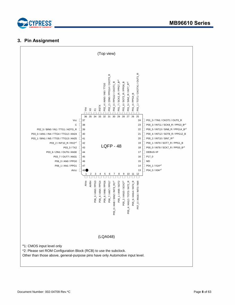
3. Pin Assignment
(Top view)
(LQA048)
*1: CMOS input level only
*2: Please set ROM Configuration Block (RCB) to use the subclock.
Other than those above, general-purpose pins have only Automotive input level.
LQFP - 48
P01_0 / TIN1 / CKOT1 / OUT0_R
P00_3 / INT11 / SCK8_R / PPG3_B*1
P00_5 / INT13 / SIN8_R / PPG14_B*1
P00_4 / INT12 / SOT8_R / PPG12_B
P00_2 / INT10 / SIN7_R*1
P00_1 / INT9 / SOT7_R / PPG1_B
P00_0 / INT8 / SCK7_R / PPG0_B*1
DEBUG I/F
P17_0
MD
P04_1 / X1A*2
P04_0 / X0A*2
Vss
X0
X1
RS
TX
P0
2_4 /
AIN
0 /
IN0 /
TT
G0
P0
2_2
/ Z
IN0
/P
PG
14
/C
KO
T0_R
P0
2_0
/P
PG
12
/C
KO
T1_
R
P0
1_7
/S
CK
2_
R /
PP
G7_B
*1
P0
1_6
/ S
OT
2_
R /
PP
G6_B
P0
1_5
/ S
IN2_
R /
IN
T7_
R*1
P0
1_4
/P
PG
4_B
P0
1_1
/T
OT
1/
CK
OT
X1
/O
UT
1_R
Vcc
C
P02_5 / BIN0 / IN1 / TTG1 / ADTG_R
P03_0 / AIN1 / IN4 / TTG4 / TTG12 / AN24
P03_1 / BIN1 / IN5 / TTG5 / TTG13 / AN25
P03_2 / INT10_R / RX2*1
P03_3 / TX2
P03_6 / ZIN1 / OUT6 / AN30
P03_7 / OUT7 / AN31
P06_0 / AN0 / PPG0
P06_1 / AN1 / PPG1
AVcc
AV
ss
AV
RH
P0
6_
3/A
N3
/P
PG
3
P0
6_
4/A
N4
/P
PG
4
P0
6_
6/A
N6
/P
PG
6
P0
6_
7/A
N7
/P
PG
7
P0
5_0
/A
N8
/S
IN2
/ IN
T3_
R1
*1
P0
5_1
/A
N9 /
SO
T2
P0
5_2
/A
N10
/ S
CK
2*1
P0
5_4
/A
N12
/T
OT
3/IN
T2_
R
P0
5_
6 /
AN
14
/ IN
T4_R
P0
7_0 /
AN
16
/ IN
T0 /
NM
I
24
23
22
21
20
19
18
17
16
15
14
13
37
38
39
40
41
42
43
44
45
46
47
48
36 35 34 33 32 31 30 29 28 27 26 25
1 2 3 4 5 6 7 8 9 10 11 12
Document Number: 002-04709 Rev.*C Page 9 of 63
MB96610 Series
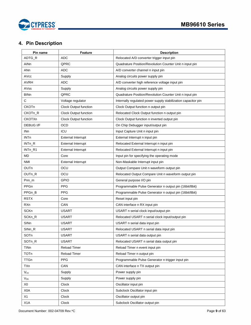
4. Pin Description
Pin name Feature Description
ADTG_R ADC Relocated A/D converter trigger input pin
AINn QPRC Quadrature Position/Revolution Counter Unit n input pin
ANn ADC A/D converter channel n input pin
AVcc Supply Analog circuits power supply pin
AVRH ADC A/D converter high reference voltage input pin
AVss Supply Analog circuits power supply pin
BINn QPRC Quadrature Position/Revolution Counter Unit n input pin
C Voltage regulator Internally regulated power supply stabilization capacitor pin
CKOTn Clock Output function Clock Output function n output pin
CKOTn_R Clock Output function Relocated Clock Output function n output pin
CKOTXn Clock Output function Clock Output function n inverted output pin
DEBUG I/F OCD On Chip Debugger input/output pin
INn ICU Input Capture Unit n input pin
INTn External Interrupt External Interrupt n input pin
INTn_R External Interrupt Relocated External Interrupt n input pin
INTn_R1 External Interrupt Relocated External Interrupt n input pin
MD Core Input pin for specifying the operating mode
NMI External Interrupt Non-Maskable Interrupt input pin
OUTn OCU Output Compare Unit n waveform output pin
OUTn_R OCU Relocated Output Compare Unit n waveform output pin
Pnn_m GPIO General purpose I/O pin
PPGn PPG Programmable Pulse Generator n output pin (16bit/8bit)
PPGn_B PPG Programmable Pulse Generator n output pin (16bit/8bit)
RSTX Core Reset input pin
RXn CAN CAN interface n RX input pin
SCKn USART USART n serial clock input/output pin
SCKn_R USART Relocated USART n serial clock input/output pin
SINn USART USART n serial data input pin
SINn_R USART Relocated USART n serial data input pin
SOTn USART USART n serial data output pin
SOTn_R USART Relocated USART n serial data output pin
TINn Reload Timer Reload Timer n event input pin
TOTn Reload Timer Reload Timer n output pin
TTGn PPG Programmable Pulse Generator n trigger input pin
TXn CAN CAN interface n TX output pin
Vcc Supply Power supply pin
Vss Supply Power supply pin
X0 Clock Oscillator input pin
X0A Clock Subclock Oscillator input pin
X1 Clock Oscillator output pin
X1A Clock Subclock Oscillator output pin
Document Number: 002-04709 Rev.*C Page 10 of 63
MB96610 Series
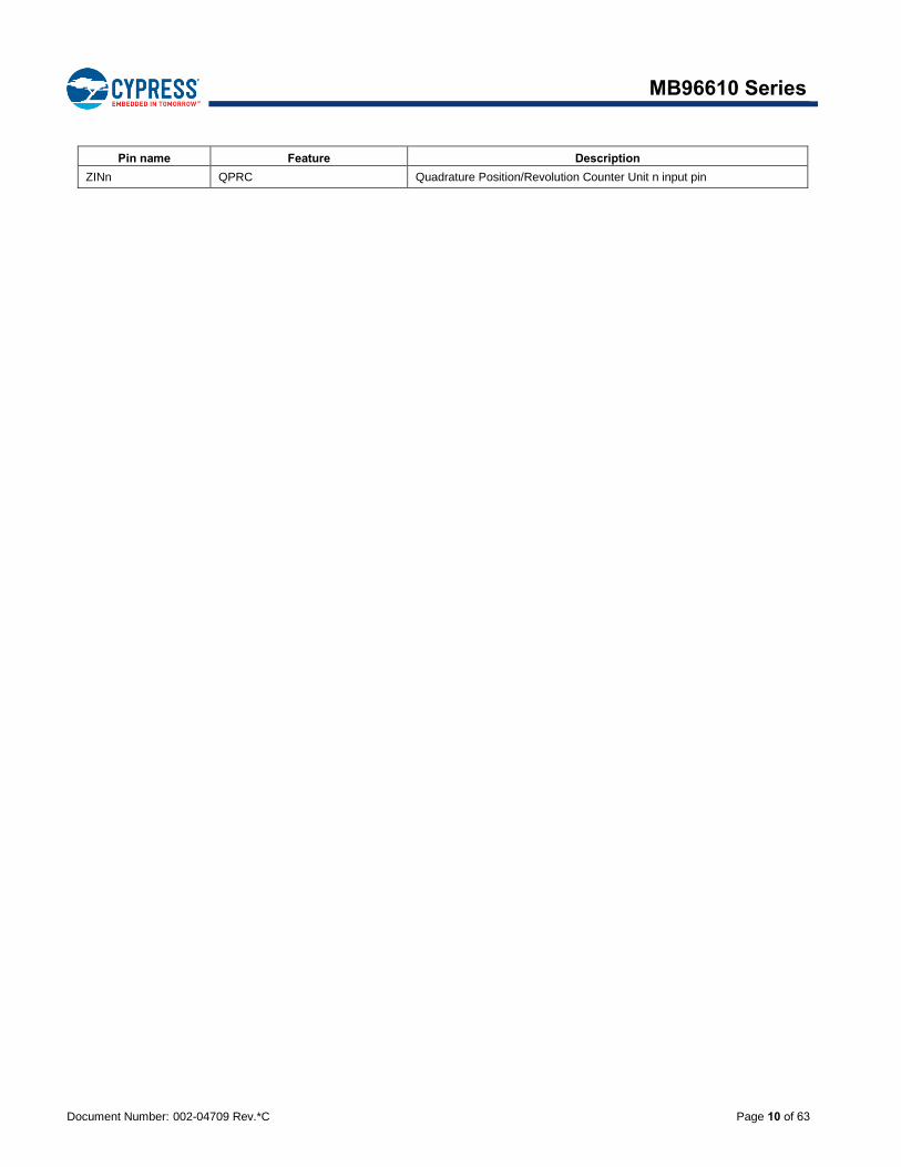
Pin name Feature Description
ZINn QPRC Quadrature Position/Revolution Counter Unit n input pin
Document Number: 002-04709 Rev.*C Page 11 of 63
MB96610 Series
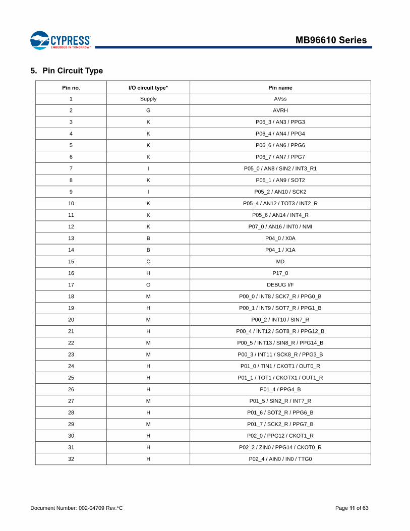
5. Pin Circuit Type
Pin no. I/O circuit type* Pin name
1 Supply AVss
2 G AVRH
3 K P06_3 / AN3 / PPG3
4 K P06_4 / AN4 / PPG4
5 K P06_6 / AN6 / PPG6
6 K P06_7 / AN7 / PPG7
7 I P05_0 / AN8 / SIN2 / INT3_R1
8 K P05_1 / AN9 / SOT2
9 I P05_2 / AN10 / SCK2
10 K P05_4 / AN12 / TOT3 / INT2_R
11 K P05_6 / AN14 / INT4_R
12 K P07_0 / AN16 / INT0 / NMI
13 B P04_0 / X0A
14 B P04_1 / X1A
15 C MD
16 H P17_0
17 O DEBUG I/F
18 M P00_0 / INT8 / SCK7_R / PPG0_B
19 H P00_1 / INT9 / SOT7_R / PPG1_B
20 M P00_2 / INT10 / SIN7_R
21 H P00_4 / INT12 / SOT8_R / PPG12_B
22 M P00_5 / INT13 / SIN8_R / PPG14_B
23 M P00_3 / INT11 / SCK8_R / PPG3_B
24 H P01_0 / TIN1 / CKOT1 / OUT0_R
25 H P01_1 / TOT1 / CKOTX1 / OUT1_R
26 H P01_4 / PPG4_B
27 M P01_5 / SIN2_R / INT7_R
28 H P01_6 / SOT2_R / PPG6_B
29 M P01_7 / SCK2_R / PPG7_B
30 H P02_0 / PPG12 / CKOT1_R
31 H P02_2 / ZIN0 / PPG14 / CKOT0_R
32 H P02_4 / AIN0 / IN0 / TTG0
Document Number: 002-04709 Rev.*C Page 12 of 63
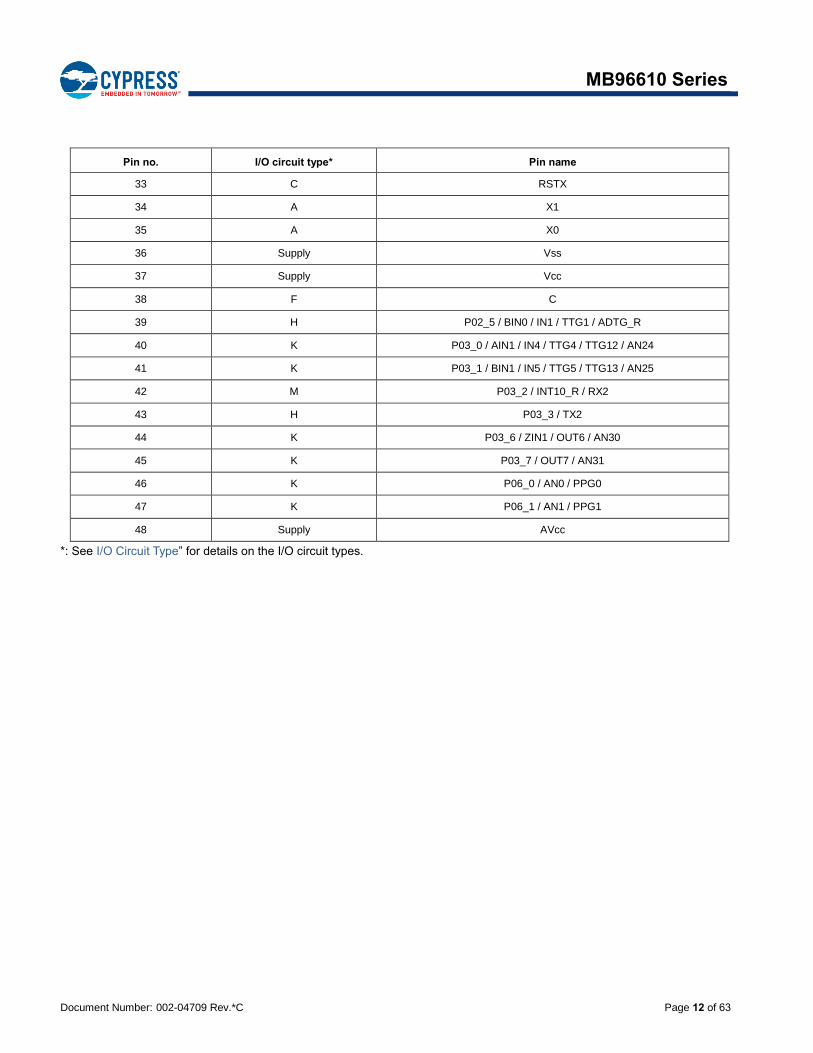
MB96610 Series
Pin no. I/O circuit type* Pin name
33 C RSTX
34 A X1
35 A X0
36 Supply Vss
37 Supply Vcc
38 F C
39 H P02_5 / BIN0 / IN1 / TTG1 / ADTG_R
40 K P03_0 / AIN1 / IN4 / TTG4 / TTG12 / AN24
41 K P03_1 / BIN1 / IN5 / TTG5 / TTG13 / AN25
42 M P03_2 / INT10_R / RX2
43 H P03_3 / TX2
44 K P03_6 / ZIN1 / OUT6 / AN30
45 K P03_7 / OUT7 / AN31
46 K P06_0 / AN0 / PPG0
47 K P06_1 / AN1 / PPG1
48 Supply AVcc
*: See I/O Circuit Type” for details on the I/O circuit types.
Document Number: 002-04709 Rev.*C Page 13 of 63
MB96610 Series
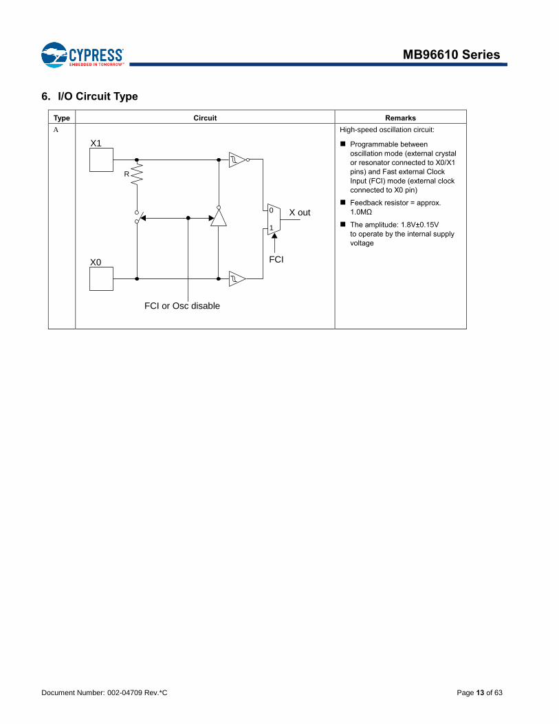
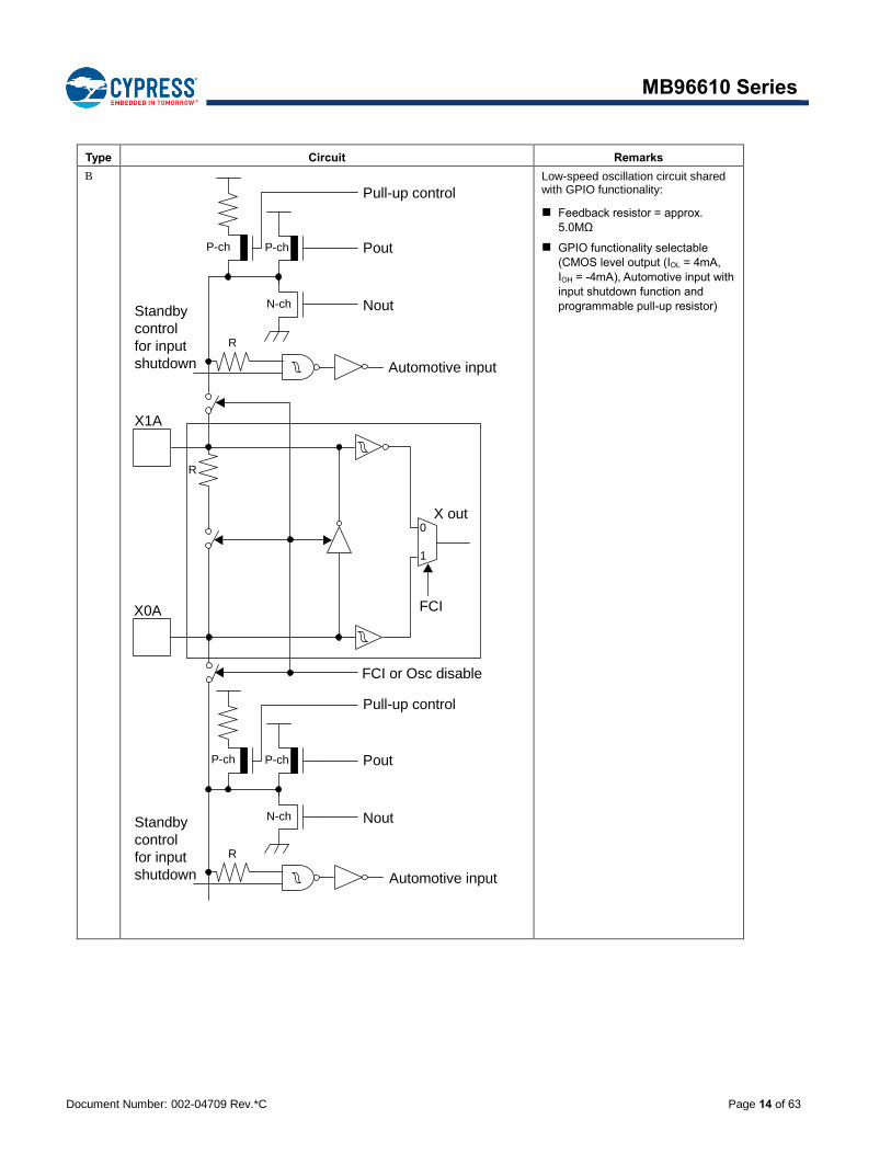
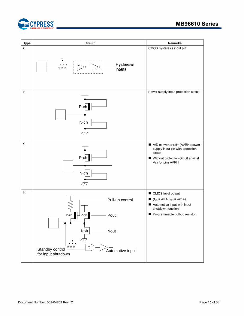
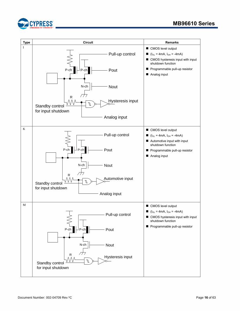
6. I/O Circuit Type
Type Circuit Remarks
A
High-speed oscillation circuit:
Programmable between
oscillation mode (external crystal
or resonator connected to X0/X1
pins) and Fast external Clock
Input (FCI) mode (external clock
connected to X0 pin)
Feedback resistor = approx.
1.0MΩ
The amplitude: 1.8V±0.15V
to operate by the internal supply
voltage
R
FCI
X out0
1
X1
X0
FCI or Osc disable
Document Number: 002-04709 Rev.*C Page 14 of 63
MB96610 Series
Type Circuit Remarks
B
Low-speed oscillation circuit shared with GPIO functionality:
Feedback resistor = approx.
5.0MΩ
GPIO functionality selectable
(CMOS level output (IOL = 4mA,
IOH = -4mA), Automotive input with
input shutdown function and
programmable pull-up resistor)
R
FCI
X out0
1
Pout
R
Nout
Automotive input
FCI or Osc disable
Standby
control
for input
shutdown
Standby
control
for input
shutdown
Automotive input
X1A
X0A
R
P-ch P-ch
N-ch
Pull-up control
Pull-up control
Pout
Nout
P-ch P-ch
N-ch
Document Number: 002-04709 Rev.*C Page 15 of 63
MB96610 Series
Type Circuit Remarks
C
CMOS hysteresis input pin
F
Power supply input protection circuit
G
A/D converter ref+ (AVRH) power
supply input pin with protection
circuit
Without protection circuit against
VCC for pins AVRH
H
CMOS level output
(IOL = 4mA, IOH = -4mA)
Automotive input with input
shutdown function
Programmable pull-up resistor
P-ch
N-ch
P-ch
N-ch
Standby control
for input shutdownAutomotive input
R
Pull-up control
Pout
Nout
P-ch P-ch
N-ch
Document Number: 002-04709 Rev.*C Page 16 of 63
MB96610 Series
Type Circuit Remarks
I
CMOS level output
(IOL = 4mA, IOH = -4mA)
CMOS hysteresis input with input
shutdown function
Programmable pull-up resistor
Analog input
K
CMOS level output
(IOL = 4mA, IOH = -4mA)
Automotive input with input
shutdown function
Programmable pull-up resistor
Analog input
M
CMOS level output
(IOL = 4mA, IOH = -4mA)
CMOS hysteresis input with input
shutdown function
Programmable pull-up resistor
Standby control
for input shutdown
R
Pull-up control
Pout
Nout
P-ch P-ch
N-ch
Analog input
Hysteresis input
Standby control
for input shutdown
R
Pull-up control
Pout
Nout
P-ch P-ch
N-ch
Analog input
Automotive input
Standby control
for input shutdown
Hysteresis inputR
Pull-up control
Pout
Nout
P-ch P-ch
N-ch
Document Number: 002-04709 Rev.*C Page 17 of 63
MB96610 Series
Type Circuit Remarks
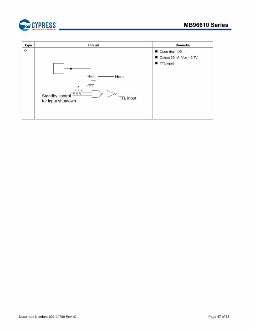
O
Open-drain I/O
Output 25mA, Vcc = 2.7V
TTL input
Standby control
for input shutdownTTL input
R
NoutN-ch
Document Number: 002-04709 Rev.*C Page 18 of 63
MB96610 Series
7. Memory Map
*1: For details about USER ROM area, see “
User ROM Memory Map for Flash Devices” on the following pages.
*2: For RAMSTART addresses, see the table on the next page.
*3: Unused GPR banks can be used as RAM area.
GPR: General-Purpose Register
The DMA area is only available if the device contains the corresponding resource.
The available RAM and ROM area depends on the device.
FF:FFFFH
DE:0000H
DD:FFFFH
10:0000H
0F:C000H
0E:9000H
01:0000H
00:8000H
RAMSTART0*2
00:0C00H
00:0380H
00:0180H
00:0100H
00:00F0H
00:0000H
GPR*3
DMA
Reserved
Peripheral
Reserved
USER ROM*1
Reserved
Boot-ROM
Peripheral
ROM/RAM
MIRROR
Internal RAM
bank0
Peripheral
Reserved
Document Number: 002-04709 Rev.*C Page 19 of 63
MB96610 Series
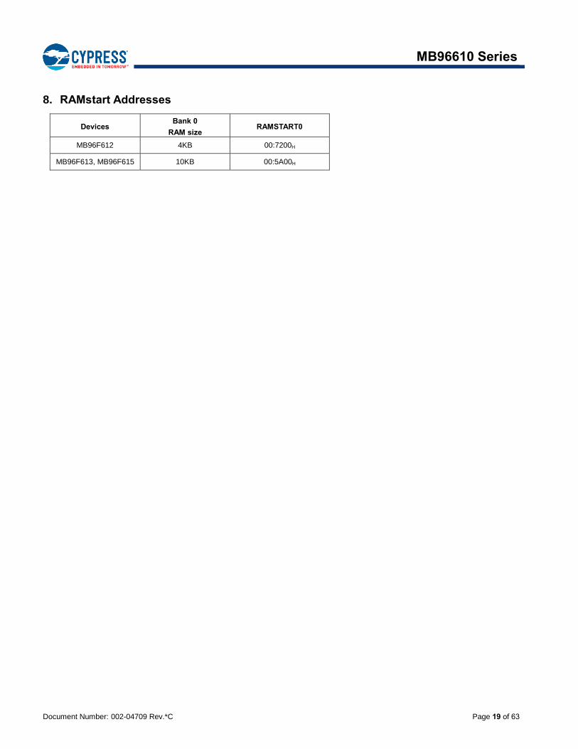
8. RAMstart Addresses
Devices Bank 0
RAM size RAMSTART0
MB96F612 4KB 00:7200H
MB96F613, MB96F615 10KB 00:5A00H
Document Number: 002-04709 Rev.*C Page 20 of 63
MB96610 Series
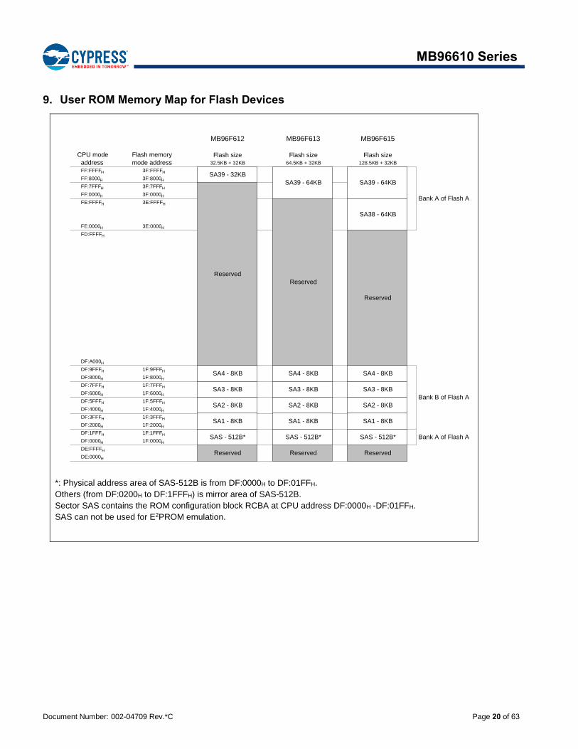
9. User ROM Memory Map for Flash Devices
*: Physical address area of SAS-512B is from DF:0000H to DF:01FFH.
Others (from DF:0200H to DF:1FFFH) is mirror area of SAS-512B.
Sector SAS contains the ROM configuration block RCBA at CPU address DF:0000H -DF:01FFH.
SAS can not be used for E2PROM emulation.
MB96F612 MB96F613 MB96F615
Flash size Flash size
32.5KB + 32KB 64.5KB + 32KB 128.5KB + 32KB
FF:FFFFH 3F:FFFFH
FF:8000H 3F:8000H
FF:7FFFH 3F:7FFFH
FF:0000H 3F:0000H
FE:FFFFH 3E:FFFFH
FE:0000H 3E:0000H
FD:FFFFH
Bank A of Flash A
SAS - 512B*
Reserved
Reserved
SA2 - 8KB
SA1 - 8KB
SA4 - 8KB
SA3 - 8KB
SA38 - 64KB
SA39 - 64KB
CPU mode
address
Flash memory
mode address
Reserved
SA4 - 8KB
SA3 - 8KB
SA2 - 8KB
SA1 - 8KB
SAS - 512B*
Reserved
SA4 - 8KB
SA3 - 8KB
Reserved
Reserved
SA39 - 32KB
SA39 - 64KB
Bank B of Flash A
Bank A of Flash ASAS - 512B*
SA2 - 8KB
SA1 - 8KB
Flash size
DF:A000H
DF:9FFFH 1F:9FFFH
DF:8000H 1F:8000H
DF:7FFFH 1F:7FFFH
DF:6000H 1F:6000H
DF:5FFFH 1F:5FFFH
DF:4000H 1F:4000H
DF:3FFFH 1F:3FFFH
DF:2000H 1F:2000H
DF:1FFFH 1F:1FFFH
DF:0000H 1F:0000H
DE:FFFFH
DE:0000H
Document Number: 002-04709 Rev.*C Page 21 of 63
MB96610 Series
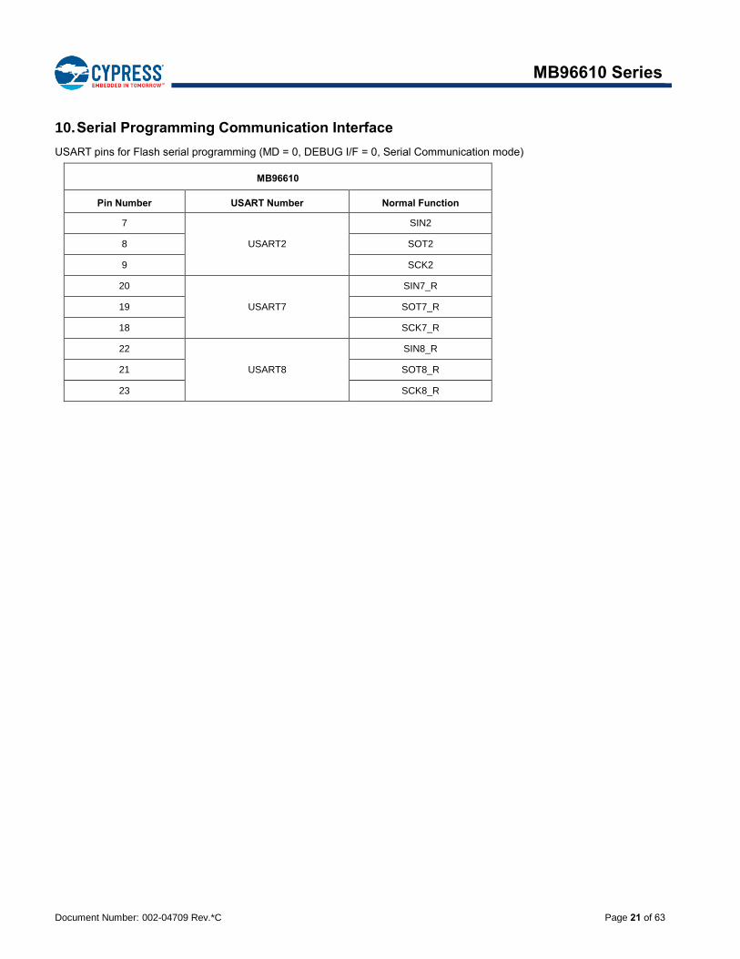
10. Serial Programming Communication Interface
USART pins for Flash serial programming (MD = 0, DEBUG I/F = 0, Serial Communication mode)
MB96610
Pin Number USART Number Normal Function
7
USART2
SIN2
8 SOT2
9 SCK2
20
USART7
SIN7_R
19 SOT7_R
18 SCK7_R
22
USART8
SIN8_R
21 SOT8_R
23 SCK8_R
Document Number: 002-04709 Rev.*C Page 22 of 63
MB96610 Series
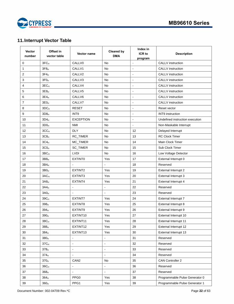
11. Interrupt Vector Table
Vector
number
Offset in
vector table Vector name
Cleared by
DMA
Index in
ICR to
program
Description
0 3FCH CALLV0 No - CALLV instruction
1 3F8H CALLV1 No - CALLV instruction
2 3F4H CALLV2 No - CALLV instruction
3 3F0H CALLV3 No - CALLV instruction
4 3ECH CALLV4 No - CALLV instruction
5 3E8H CALLV5 No - CALLV instruction
6 3E4H CALLV6 No - CALLV instruction
7 3E0H CALLV7 No - CALLV instruction
8 3DCH RESET No - Reset vector
9 3D8H INT9 No - INT9 instruction
10 3D4H EXCEPTION No - Undefined instruction execution
11 3D0H NMI No - Non-Maskable Interrupt
12 3CCH DLY No 12 Delayed Interrupt
13 3C8H RC_TIMER No 13 RC Clock Timer
14 3C4H MC_TIMER No 14 Main Clock Timer
15 3C0H SC_TIMER No 15 Sub Clock Timer
16 3BCH LVDI No 16 Low Voltage Detector
17 3B8H EXTINT0 Yes 17 External Interrupt 0
18 3B4H - - 18 Reserved
19 3B0H EXTINT2 Yes 19 External Interrupt 2
20 3ACH EXTINT3 Yes 20 External Interrupt 3
21 3A8H EXTINT4 Yes 21 External Interrupt 4
22 3A4H - - 22 Reserved
23 3A0H - - 23 Reserved
24 39CH EXTINT7 Yes 24 External Interrupt 7
25 398H EXTINT8 Yes 25 External Interrupt 8
26 394H EXTINT9 Yes 26 External Interrupt 9
27 390H EXTINT10 Yes 27 External Interrupt 10
28 38CH EXTINT11 Yes 28 External Interrupt 11
29 388H EXTINT12 Yes 29 External Interrupt 12
30 384H EXTINT13 Yes 30 External Interrupt 13
31 380H - - 31 Reserved
32 37CH - - 32 Reserved
33 378H - - 33 Reserved
34 374H - - 34 Reserved
35 370H CAN2 No 35 CAN Controller 2
36 36CH - - 36 Reserved
37 368H - - 37 Reserved
38 364H PPG0 Yes 38 Programmable Pulse Generator 0
39 360H PPG1 Yes 39 Programmable Pulse Generator 1
Document Number: 002-04709 Rev.*C Page 23 of 63
MB96610 Series
Vector
number
Offset in
vector table Vector name
Cleared by
DMA
Index in
ICR to
program
Description
40 35CH - - 40 Reserved
41 358H PPG3 Yes 41 Programmable Pulse Generator 3
42 354H PPG4 Yes 42 Programmable Pulse Generator 4
43 350H - - 43 Reserved
44 34CH PPG6 Yes 44 Programmable Pulse Generator 6
45 348H PPG7 Yes 45 Programmable Pulse Generator 7
46 344H - - 46 Reserved
47 340H - - 47 Reserved
48 33CH - - 48 Reserved
49 338H - - 49 Reserved
50 334H PPG12 Yes 50 Programmable Pulse Generator 12
51 330H - - 51 Reserved
52 32CH PPG14 Yes 52 Programmable Pulse Generator 14
53 328H - - 53 Reserved
54 324H - - 54 Reserved
55 320H - - 55 Reserved
56 31CH - - 56 Reserved
57 318H - - 57 Reserved
58 314H - - 58 Reserved
59 310H RLT1 Yes 59 Reload Timer 1
60 30CH - - 60 Reserved
61 308H RLT3 Yes 61 Reload Timer 3
62 304H - - 62 Reserved
63 300H - - 63 Reserved
64 2FCH RLT6 Yes 64 Reload Timer 6
65 2F8H ICU0 Yes 65 Input Capture Unit 0
66 2F4H ICU1 Yes 66 Input Capture Unit 1
67 2F0H - - 67 Reserved
68 2ECH - - 68 Reserved
69 2E8H ICU4 Yes 69 Input Capture Unit 4
70 2E4H ICU5 Yes 70 Input Capture Unit 5
71 2E0H ICU6 Yes 71 Input Capture Unit 6
72 2DCH - - 72 Reserved
73 2D8H - - 73 Reserved
74 2D4H ICU9 Yes 74 Input Capture Unit 9
75 2D0H ICU10 Yes 75 Input Capture Unit 10
76 2CCH - - 76 Reserved
77 2C8H OCU0 Yes 77 Output Compare Unit 0
78 2C4H OCU1 Yes 78 Output Compare Unit 1
79 2C0H - - 79 Reserved
80 2BCH - - 80 Reserved
Document Number: 002-04709 Rev.*C Page 24 of 63
MB96610 Series
Vector
number
Offset in
vector table Vector name
Cleared by
DMA
Index in
ICR to
program
Description
81 2B8H OCU4 Yes 81 Output Compare Unit 4
82 2B4H - - 82 Reserved
83 2B0H OCU6 Yes 83 Output Compare Unit 6
84 2ACH OCU7 Yes 84 Output Compare Unit 7
85 2A8H - - 85 Reserved
86 2A4H - - 86 Reserved
87 2A0H - - 87 Reserved
88 29CH - - 88 Reserved
89 298H FRT0 Yes 89 Free-Running Timer 0
90 294H FRT1 Yes 90 Free-Running Timer 1
91 290H FRT2 Yes 91 Free-Running Timer 2
92 28CH FRT3 Yes 92 Free-Running Timer 3
93 288H RTC0 No 93 Real Time Clock
94 284H CAL0 No 94 Clock Calibration Unit
95 280H - - 95 Reserved
96 27CH - - 96 Reserved
97 278H - - 97 Reserved
98 274H ADC0 Yes 98 A/D Converter 0
99 270H - - 99 Reserved
100 26CH - - 100 Reserved
101 268H - - 101 Reserved
102 264H - - 102 Reserved
103 260H - - 103 Reserved
104 25CH - - 104 Reserved
105 258H LINR2 Yes 105 LIN USART 2 RX
106 254H LINT2 Yes 106 LIN USART 2 TX
107 250H - - 107 Reserved
108 24CH - - 108 Reserved
109 248H - - 109 Reserved
110 244H - - 110 Reserved
111 240H - - 111 Reserved
112 23CH - - 112 Reserved
113 238H - - 113 Reserved
114 234H - - 114 Reserved
115 230H LINR7 Yes 115 LIN USART 7 RX
116 22CH LINT7 Yes 116 LIN USART 7 TX
117 228H LINR8 Yes 117 LIN USART 8 RX
118 224H LINT8 Yes 118 LIN USART 8 TX
119 220H - - 119 Reserved
120 21CH - - 120 Reserved
121 218H - - 121 Reserved
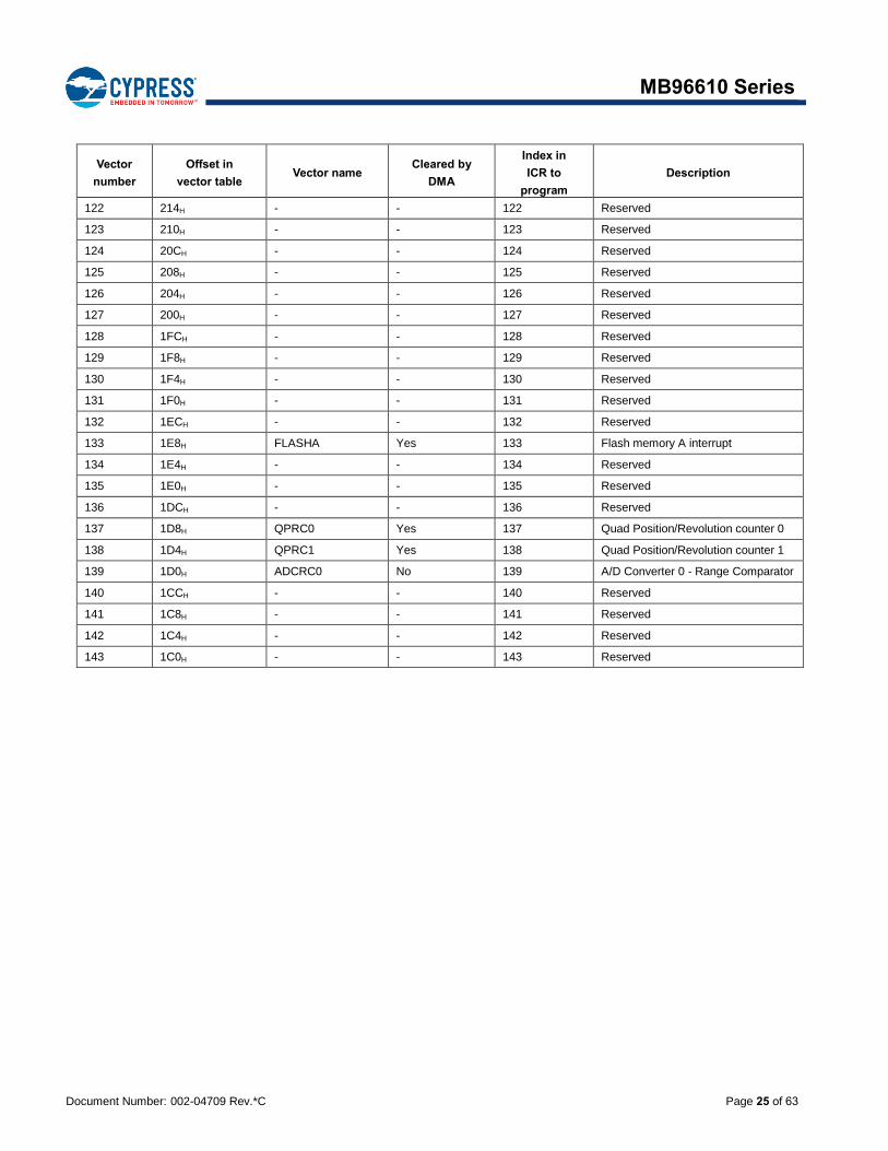
Document Number: 002-04709 Rev.*C Page 25 of 63
MB96610 Series
Vector
number
Offset in
vector table Vector name
Cleared by
DMA
Index in
ICR to
program
Description
122 214H - - 122 Reserved
123 210H - - 123 Reserved
124 20CH - - 124 Reserved
125 208H - - 125 Reserved
126 204H - - 126 Reserved
127 200H - - 127 Reserved
128 1FCH - - 128 Reserved
129 1F8H - - 129 Reserved
130 1F4H - - 130 Reserved
131 1F0H - - 131 Reserved
132 1ECH - - 132 Reserved
133 1E8H FLASHA Yes 133 Flash memory A interrupt
134 1E4H - - 134 Reserved
135 1E0H - - 135 Reserved
136 1DCH - - 136 Reserved
137 1D8H QPRC0 Yes 137 Quad Position/Revolution counter 0
138 1D4H QPRC1 Yes 138 Quad Position/Revolution counter 1
139 1D0H ADCRC0 No 139 A/D Converter 0 - Range Comparator
140 1CCH - - 140 Reserved
141 1C8H - - 141 Reserved
142 1C4H - - 142 Reserved
143 1C0H - - 143 Reserved
Document Number: 002-04709 Rev.*C Page 26 of 63
MB96610 Series
12. Handling Precautions
Any semiconductor devices have inherently a certain rate of failure. The possibility of failure is greatly affected by the conditions in
which they are used (circuit conditions, environmental conditions, etc.). This page describes precautions that must be observed to
minimize the chance of failure and to obtain higher reliability from your Cypress semiconductor devices.
12.1 Precautions for Product Design
This section describes precautions when designing electronic equipment using semiconductor devices.
Absolute Maximum Ratings
Semiconductor devices can be permanently damaged by application of stress (voltage, current, temperature, etc.) in excess of
certain established limits, called absolute maximum ratings. Do not exceed these ratings.
Recommended Operating Conditions
Recommended operating conditions are normal operating ranges for the semiconductor device. All the device's electrical
characteristics are warranted when operated within these ranges.
Always use semiconductor devices within the recommended operating conditions. Operation outside these ranges may adversely
affect reliability and could result in device failure.
No warranty is made with respect to uses, operating conditions, or combinations not represented on the data sheet. Users
considering application outside the listed conditions are advised to contact their sales representative beforehand.
Processing and Protection of Pins These precautions must be followed when handling the pins which connect semiconductor devices to power supply and input/output functions.
1. Preventing Over-Voltage and Over-Current Conditions
Exposure to voltage or current levels in excess of maximum ratings at any pin is likely to cause deterioration within the device, and in extreme cases leads to permanent damage of the device. Try to prevent such overvoltage or over-current conditions at the design stage.
2. Protection of Output Pins
Shorting of output pins to supply pins or other output pins, or connection to large capacitance can cause large current flows. Such conditions if present for extended periods of time can damage the device. Therefore, avoid this type of connection.
3. Handling of Unused Input Pins
Unconnected input pins with very high impedance levels can adversely affect stability of operation. Such pins should be connected through an appropriate resistance to a power supply pin or ground pin.
Latch-up Semiconductor devices are constructed by the formation of P-type and N-type areas on a substrate. When subjected to abnormally high voltages, internal parasitic PNPN junctions (called thyristor structures) may be formed, causing large current levels in excess of several hundred mA to flow continuously at the power supply pin. This condition is called latch-up.
Document Number: 002-04709 Rev.*C Page 27 of 63
MB96610 Series
CAUTION: The occurrence of latch-up not only causes loss of reliability in the semiconductor device, but can cause injury or damage from high heat, smoke or flame. To prevent this from happening, do the following:
1. Be sure that voltages applied to pins do not exceed the absolute maximum ratings. This should include attention to abnormal
noise, surge levels, etc.
2. Be sure that abnormal current flows do not occur during the power-on sequence.
Observance of Safety Regulations and Standards
Most countries in the world have established standards and regulations regarding safety, protection from electromagnetic
interference, etc. Customers are requested to observe applicable regulations and standards in the design of products.
Fail-Safe Design
Any semiconductor devices have inherently a certain rate of failure. You must protect against injury, damage or loss from such
failures by incorporating safety design measures into your facility and equipment such as redundancy, fire protection, and
prevention of over-current levels and other abnormal operating conditions.
Precautions Related to Usage of Devices
Cypress semiconductor devices are intended for use in standard applications (computers, office automation and other office
equipment, industrial, communications, and measurement equipment, personal or household devices, etc.).
CAUTION:
Customers considering the use of our products in special applications where failure or abnormal operation may directly affect
human lives or cause physical injury or property damage, or where extremely high levels of reliability are demanded (such as
aerospace systems, atomic energy controls, sea floor repeaters, vehicle operating controls, medical devices for life support, etc.)
are requested to consult with sales representatives before such use. The company will not be responsible for damages arising
from such use without prior approval.
12.2 Precautions for Package Mounting
Package mounting may be either lead insertion type or surface mount type. In either case, for heat resistance during soldering, you
should only mount under Cypress's recommended conditions. For detailed information about mount conditions, contact your sales
representative.
Lead Insertion Type
Mounting of lead insertion type packages onto printed circuit boards may be done by two methods: direct soldering on the board,
or mounting by using a socket.
Direct mounting onto boards normally involves processes for inserting leads into through-holes on the board and using the flow
soldering (wave soldering) method of applying liquid solder. In this case, the soldering process usually causes leads to be
subjected to thermal stress in excess of the absolute ratings for storage temperature. Mounting processes should conform to
Cypress recommended mounting conditions.
If socket mounting is used, differences in surface treatment of the socket contacts and IC lead surfaces can lead to contact
deterioration after long periods. For this reason it is recommended that the surface treatment of socket contacts and IC leads be
verified before mounting.
Document Number: 002-04709 Rev.*C Page 28 of 63
MB96610 Series
Surface Mount Type
Surface mount packaging has longer and thinner leads than lead-insertion packaging, and therefore leads are more easily
deformed or bent. The use of packages with higher pin counts and narrower pin pitch results in increased susceptibility to open
connections caused by deformed pins, or shorting due to solder bridges.
You must use appropriate mounting techniques. Cypress recommends the solder reflow method, and has established a ranking of
mounting conditions for each product. Users are advised to mount packages in accordance with Cypress ranking of recommended
conditions.
Lead-Free Packaging
CAUTION:
When ball grid array (BGA) packages with Sn-Ag-Cu balls are mounted using Sn-Pb eutectic soldering, junction strength may be
reduced under some conditions of use.
Storage of Semiconductor Devices
Because plastic chip packages are formed from plastic resins, exposure to natural environmental conditions will cause absorption
of moisture. During mounting, the application of heat to a package that has absorbed moisture can cause surfaces to peel,
reducing moisture resistance and causing packages to crack. To prevent, do the following:
1. Avoid exposure to rapid temperature changes, which cause moisture to condense inside the product. Store products in locations where temperature changes are slight.
2. Use dry boxes for product storage. Products should be stored below 70% relative humidity, and at temperatures between 5°C
and 30°C.When you open Dry Package that recommends humidity 40% to 70% relative humidity.
3. When necessary, Cypress packages semiconductor devices in highly moisture-resistant aluminum laminate bags, with a silica
gel desiccant. Devices should be sealed in their aluminum laminate bags for storage.
4. Avoid storing packages where they are exposed to corrosive gases or high levels of dust.
Baking
Packages that have absorbed moisture may be de-moisturized by baking (heat drying). Follow the Cypress recommended
conditions for baking.
Condition: 125°C/24 h
Static Electricity
Because semiconductor devices are particularly susceptible to damage by static electricity, you must take the following
precautions:
1. Maintain relative humidity in the working environment between 40% and 70%. Use of an apparatus for ion generation may be
needed to remove electricity.
2. Electrically ground all conveyors, solder vessels, soldering irons and peripheral equipment.
3. Eliminate static body electricity by the use of rings or bracelets connected to ground through high resistance (on the level of 1
MΩ).Wearing of conductive clothing and shoes, use of conductive floor mats and other measures to minimize shock loads is
recommended.
4. Ground all fixtures and instruments, or protect with anti-static measures.
5. Avoid the use of styro foam or other highly static-prone materials for storage of completed board assemblies.
Document Number: 002-04709 Rev.*C Page 29 of 63
MB96610 Series
12.3 Precautions for Use Environment
Reliability of semiconductor devices depends on ambient temperature and other conditions as described above.
For reliable performance, do the following:
1. Humidity
Prolonged use in high humidity can lead to leakage in devices as well as printed circuit boards. If high humidity levels are anticipated, consider anti-humidity processing.
2. Discharge of Static Electricity
When high-voltage charges exist close to semiconductor devices, discharges can cause abnormal operation. In such cases, use anti-static measures or processing to prevent discharges.
3. Corrosive Gases, Dust, or Oil
Exposure to corrosive gases or contact with dust or oil may lead to chemical reactions that will adversely affect the device. If you use devices in such conditions, consider ways to prevent such exposure or to protect the devices.
4. Radiation, Including Cosmic Radiation
Most devices are not designed for environments involving exposure to radiation or cosmic radiation. Users should provide shielding as appropriate.
5. Smoke, Flame
CAUTION:
Plastic molded devices are flammable, and therefore should not be used near combustible substances. If devices begin to smoke
or burn, there is danger of the release of toxic gases.
Customers considering the use of Cypress products in other special environmental conditions should consult with sales representatives.
Document Number: 002-04709 Rev.*C Page 30 of 63
MB96610 Series
13. Handling Devices
Special care is required for the following when handling the device:
Latch-up prevention
Unused pins handling
External clock usage
Notes on PLL clock mode operation
Power supply pins (Vcc/Vss)
Crystal oscillator and ceramic resonator circuit
Turn on sequence of power supply to A/D converter and analog inputs
Pin handling when not using the A/D converter
Notes on Power-on
Stabilization of power supply voltage
Serial communication
Mode Pin (MD)
13.1 Latch-up prevention
CMOS IC chips may suffer latch-up under the following conditions:
A voltage higher than VCC or lower than VSS is applied to an input or output pin.
A voltage higher than the rated voltage is applied between Vcc pins and Vss pins.
The AVCC power supply is applied before the VCC voltage. Latch-up may increase the power supply current dramatically, causing thermal damages to the device.
For the same reason, extra care is required to not let the analog power-supply voltage (AVCC, AVRH) exceed
the digital power-supply voltage.
13.2 Unused pins handling Unused input pins can be left open when the input is disabled (corresponding bit of Port Input Enable register
PIER = 0).
Leaving unused input pins open when the input is enabled may result in misbehavior and possible permanent
damage of the device. To prevent latch-up, they must therefore be pulled up or pulled down through resistors which should be more
than 2k.
Unused bidirectional pins can be set either to the output state and be then left open, or to the input state with
either input disabled or external pull-up/pull-down resistor as described above.
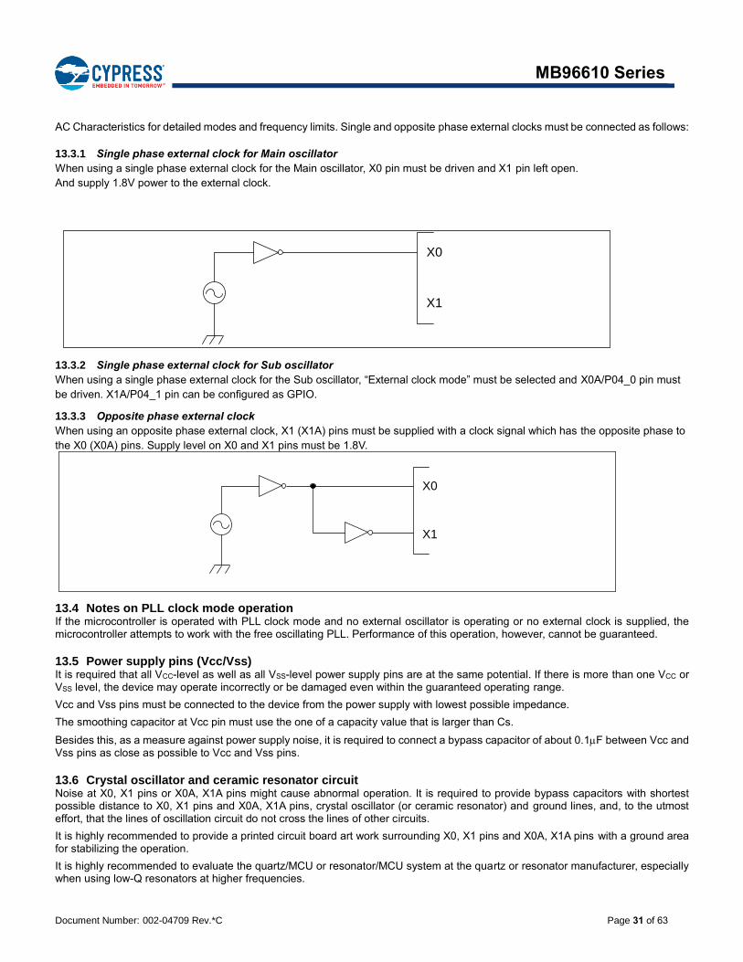
13.3 External clock usage The permitted frequency range of an external clock depends on the oscillator type and configuration.
See
Document Number: 002-04709 Rev.*C Page 31 of 63
MB96610 Series
AC Characteristics for detailed modes and frequency limits. Single and opposite phase external clocks must be connected as follows:
13.3.1 Single phase external clock for Main oscillator
When using a single phase external clock for the Main oscillator, X0 pin must be driven and X1 pin left open.
And supply 1.8V power to the external clock.
13.3.2 Single phase external clock for Sub oscillator
When using a single phase external clock for the Sub oscillator, “External clock mode” must be selected and X0A/P04_0 pin must
be driven. X1A/P04_1 pin can be configured as GPIO.
13.3.3 Opposite phase external clock
When using an opposite phase external clock, X1 (X1A) pins must be supplied with a clock signal which has the opposite phase to
the X0 (X0A) pins. Supply level on X0 and X1 pins must be 1.8V.
13.4 Notes on PLL clock mode operation If the microcontroller is operated with PLL clock mode and no external oscillator is operating or no external clock is supplied, the microcontroller attempts to work with the free oscillating PLL. Performance of this operation, however, cannot be guaranteed.
13.5 Power supply pins (Vcc/Vss) It is required that all VCC-level as well as all VSS-level power supply pins are at the same potential. If there is more than one VCC or VSS level, the device may operate incorrectly or be damaged even within the guaranteed operating range.
Vcc and Vss pins must be connected to the device from the power supply with lowest possible impedance.
The smoothing capacitor at Vcc pin must use the one of a capacity value that is larger than Cs.
Besides this, as a measure against power supply noise, it is required to connect a bypass capacitor of about 0.1F between Vcc and Vss pins as close as possible to Vcc and Vss pins.
13.6 Crystal oscillator and ceramic resonator circuit Noise at X0, X1 pins or X0A, X1A pins might cause abnormal operation. It is required to provide bypass capacitors with shortest possible distance to X0, X1 pins and X0A, X1A pins, crystal oscillator (or ceramic resonator) and ground lines, and, to the utmost effort, that the lines of oscillation circuit do not cross the lines of other circuits.
It is highly recommended to provide a printed circuit board art work surrounding X0, X1 pins and X0A, X1A pins with a ground area for stabilizing the operation.
It is highly recommended to evaluate the quartz/MCU or resonator/MCU system at the quartz or resonator manufacturer, especially when using low-Q resonators at higher frequencies.
X0
X1
X0
X1
Document Number: 002-04709 Rev.*C Page 32 of 63
MB96610 Series
13.7 Turn on sequence of power supply to A/D converter and analog inputs It is required to turn the A/D converter power supply (AVCC, AVRH) and analog inputs (ANn) on after turning the digital power supply (VCC) on.
It is also required to turn the digital power off after turning the A/D converter supply and analog inputs off. In this case, AVRH must not exceed AVCC Input voltage for ports shared with analog input ports also must not exceed AVCC (turning the analog and digital power supplies simultaneously on or off is acceptable)
13.8 Pin handling when not using the A/D converter If the A/D converter is not used, the power supply pins for A/D converter should be connected such as AVCC = VCC AVSS = AVRH = VSS.
13.9 Notes on Power-on To prevent malfunction of the internal voltage regulator, supply voltage profile while turning the power supply on should be slower
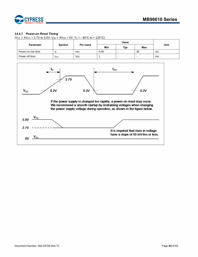
than 50s from 0.2V to 2.7V.
13.10 Stabilization of power supply voltage If the power supply voltage varies acutely even within the operation safety range of the VCC power supply voltage, a malfunction may occur. The VCC power supply voltage must therefore be stabilized. As stabilization guidelines, the power supply voltage must be stabilized in such a way that VCC ripple fluctuations (peak to peak value) in the commercial frequencies (50Hz to 60Hz) fall within
10% of the standard VCC power supply voltage and the transient fluctuation rate becomes 0.1V/s or less in instantaneous fluctuation for power supply switching.
13.11 Serial communication There is a possibility to receive wrong data due to noise or other causes on the serial communication.
Therefore, design a printed circuit board so as to avoid noise.
Consider receiving of wrong data when designing the system. For example apply a checksum and retransmit the data if an error occurs.
13.12 Mode Pin (MD) Connect the mode pin directly to Vcc or Vss pin. To prevent the device unintentionally entering test mode due to noise, lay out the printed circuit board so as to minimize the distance from the mode pin to Vcc or Vss pin and provide a low-impedance connection.
Document Number: 002-04709 Rev.*C Page 33 of 63
MB96610 Series
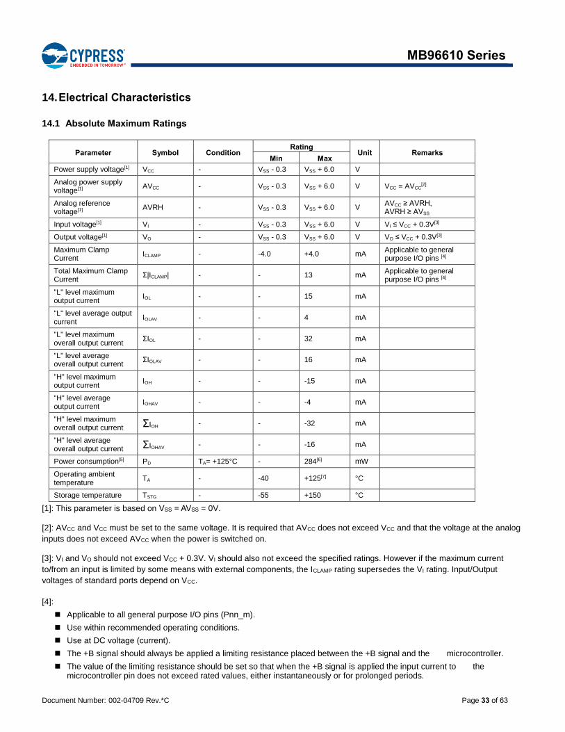
14. Electrical Characteristics
14.1 Absolute Maximum Ratings
Parameter Symbol Condition Rating
Unit Remarks Min Max
Power supply voltage[1] VCC - VSS - 0.3 VSS + 6.0 V
Analog power supply voltage[1]
AVCC - VSS - 0.3 VSS + 6.0 V VCC = AVCC[2]
Analog reference voltage[1]
AVRH - VSS - 0.3 VSS + 6.0 V AVCC ≥ AVRH, AVRH ≥ AVSS
Input voltage[1] VI - VSS - 0.3 VSS + 6.0 V VI ≤ VCC + 0.3V[3]
Output voltage[1] VO - VSS - 0.3 VSS + 6.0 V VO ≤ VCC + 0.3V[3]
Maximum Clamp Current
ICLAMP - -4.0 +4.0 mA Applicable to general purpose I/O pins [4]
Total Maximum Clamp Current
Σ|ICLAMP| - - 13 mA Applicable to general purpose I/O pins [4]
"L" level maximum output current
IOL - - 15 mA
"L" level average output current
IOLAV - - 4 mA
"L" level maximum overall output current
ΣIOL - - 32 mA
"L" level average overall output current
ΣIOLAV - - 16 mA
"H" level maximum output current
IOH - - -15 mA
"H" level average output current
IOHAV - - -4 mA
"H" level maximum overall output current ΣIOH - - -32 mA
"H" level average overall output current ΣIOHAV - - -16 mA
Power consumption[5] PD TA= +125°C - 284[6] mW
Operating ambient temperature
TA - -40 +125[7] °C
Storage temperature TSTG - -55 +150 °C
[1]: This parameter is based on VSS = AVSS = 0V.
[2]: AVCC and VCC must be set to the same voltage. It is required that AVCC does not exceed VCC and that the voltage at the analog
inputs does not exceed AVCC when the power is switched on.
[3]: VI and VO should not exceed VCC + 0.3V. VI should also not exceed the specified ratings. However if the maximum current
to/from an input is limited by some means with external components, the ICLAMP rating supersedes the VI rating. Input/Output
voltages of standard ports depend on VCC.
[4]:
Applicable to all general purpose I/O pins (Pnn_m).
Use within recommended operating conditions.
Use at DC voltage (current).
The +B signal should always be applied a limiting resistance placed between the +B signal and the microcontroller.
The value of the limiting resistance should be set so that when the +B signal is applied the input current to the microcontroller pin does not exceed rated values, either instantaneously or for prolonged periods.
Document Number: 002-04709 Rev.*C Page 34 of 63
MB96610 Series
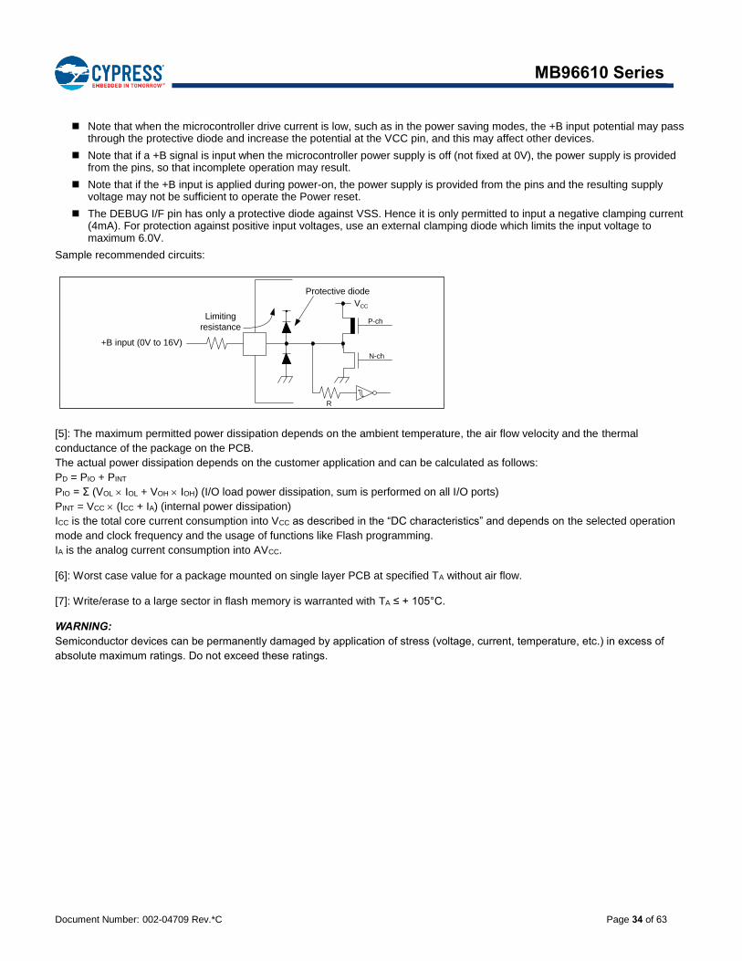
Note that when the microcontroller drive current is low, such as in the power saving modes, the +B input potential may pass through the protective diode and increase the potential at the VCC pin, and this may affect other devices.
Note that if a +B signal is input when the microcontroller power supply is off (not fixed at 0V), the power supply is provided from the pins, so that incomplete operation may result.
Note that if the +B input is applied during power-on, the power supply is provided from the pins and the resulting supply voltage may not be sufficient to operate the Power reset.
The DEBUG I/F pin has only a protective diode against VSS. Hence it is only permitted to input a negative clamping current (4mA). For protection against positive input voltages, use an external clamping diode which limits the input voltage to maximum 6.0V.
Sample recommended circuits:
[5]: The maximum permitted power dissipation depends on the ambient temperature, the air flow velocity and the thermal
conductance of the package on the PCB.
The actual power dissipation depends on the customer application and can be calculated as follows:
PD = PIO + PINT
PIO = Σ (VOL IOL + VOH IOH) (I/O load power dissipation, sum is performed on all I/O ports)
PINT = VCC (ICC + IA) (internal power dissipation)
ICC is the total core current consumption into VCC as described in the “DC characteristics” and depends on the selected operation
mode and clock frequency and the usage of functions like Flash programming.
IA is the analog current consumption into AVCC.
[6]: Worst case value for a package mounted on single layer PCB at specified TA without air flow.
[7]: Write/erase to a large sector in flash memory is warranted with TA ≤ + 105°C.
WARNING:
Semiconductor devices can be permanently damaged by application of stress (voltage, current, temperature, etc.) in excess of
absolute maximum ratings. Do not exceed these ratings.
VCC
R
+B input (0V to 16V)
Limiting
resistance
Protective diode
P-ch
N-ch
Document Number: 002-04709 Rev.*C Page 35 of 63
MB96610 Series
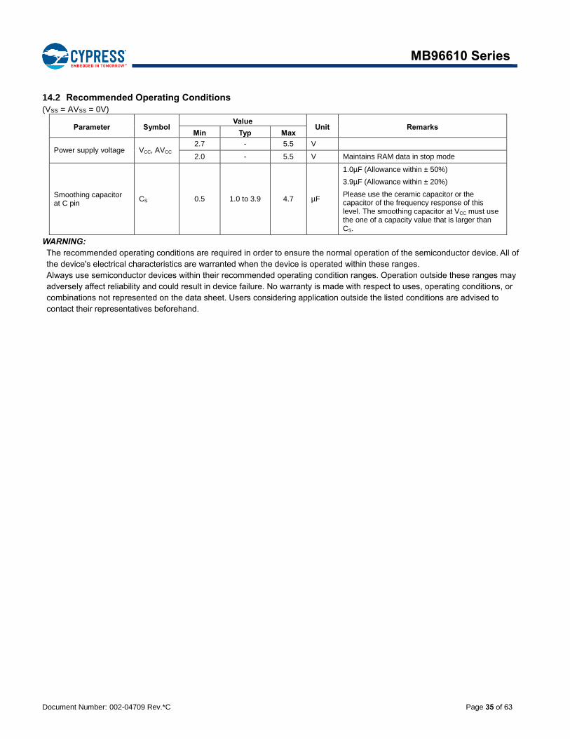
14.2 Recommended Operating Conditions
(VSS = AVSS = 0V)
Parameter Symbol Value
Unit Remarks Min Typ Max
Power supply voltage VCC, AVCC 2.7 - 5.5 V
2.0 - 5.5 V Maintains RAM data in stop mode
Smoothing capacitor at C pin
CS 0.5 1.0 to 3.9 4.7 µF
1.0µF (Allowance within ± 50%)
3.9µF (Allowance within ± 20%)
Please use the ceramic capacitor or the capacitor of the frequency response of this level. The smoothing capacitor at VCC must use the one of a capacity value that is larger than CS.
WARNING:
The recommended operating conditions are required in order to ensure the normal operation of the semiconductor device. All of
the device's electrical characteristics are warranted when the device is operated within these ranges.
Always use semiconductor devices within their recommended operating condition ranges. Operation outside these ranges may
adversely affect reliability and could result in device failure. No warranty is made with respect to uses, operating conditions, or
combinations not represented on the data sheet. Users considering application outside the listed conditions are advised to
contact their representatives beforehand.
Document Number: 002-04709 Rev.*C Page 36 of 63
MB96610 Series
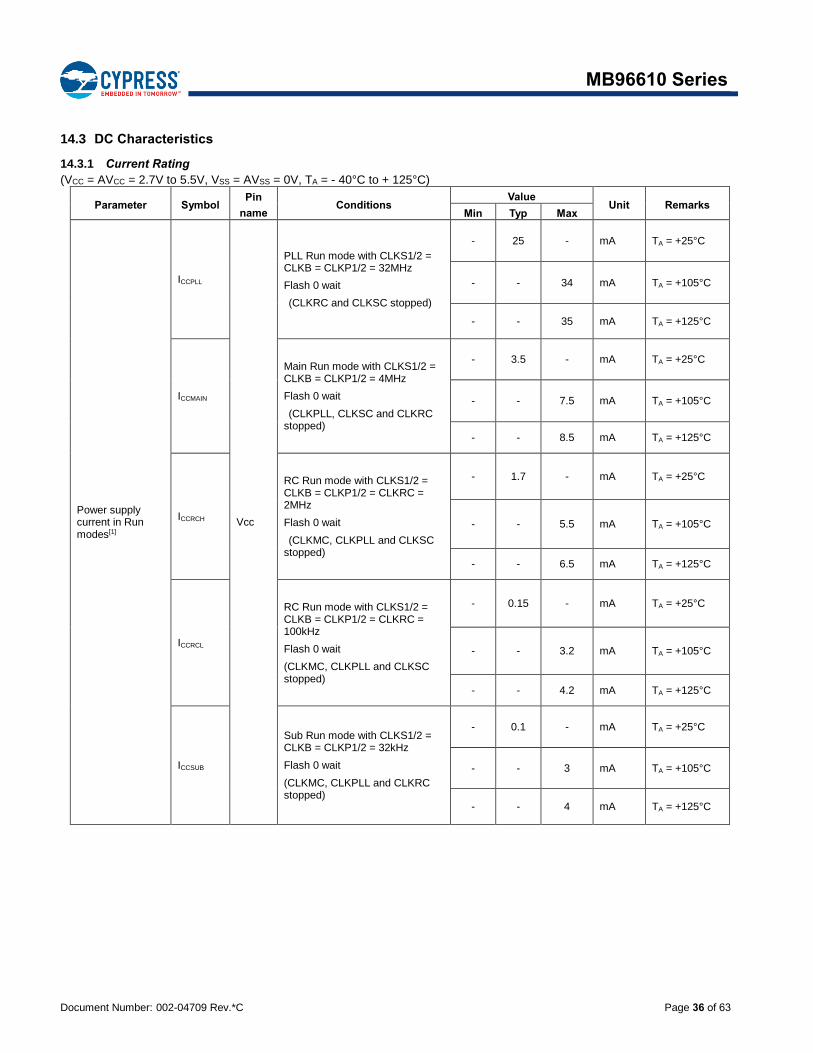
14.3 DC Characteristics
14.3.1 Current Rating
(VCC = AVCC = 2.7V to 5.5V, VSS = AVSS = 0V, TA = - 40°C to + 125°C)
Parameter Symbol Pin
name Conditions
Value Unit Remarks
Min Typ Max
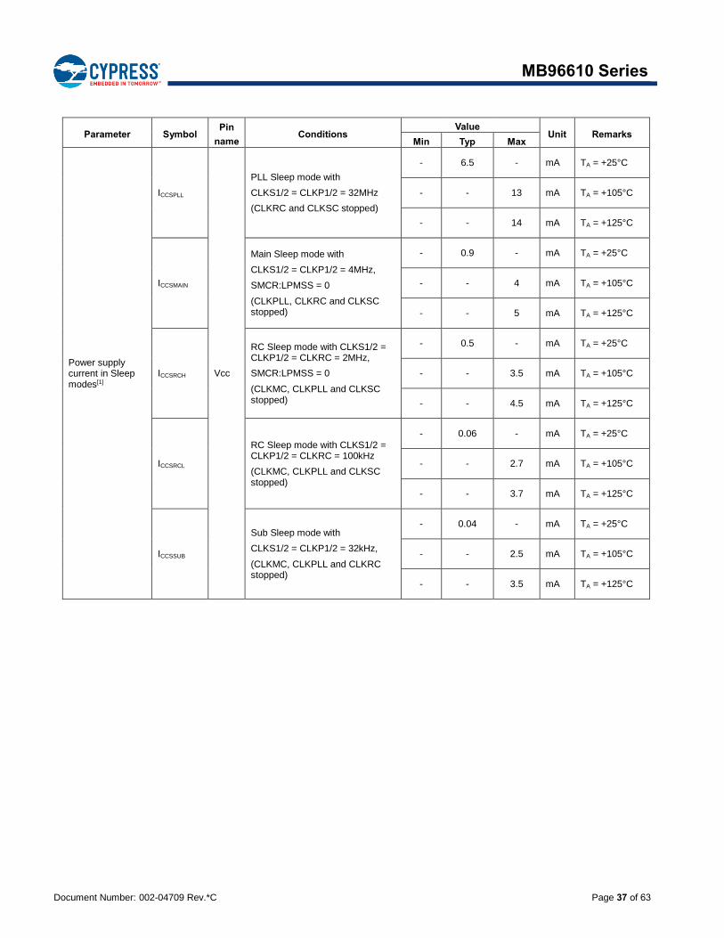
Power supply current in Run modes[1]
ICCPLL
Vcc
PLL Run mode with CLKS1/2 = CLKB = CLKP1/2 = 32MHz
Flash 0 wait
(CLKRC and CLKSC stopped)
- 25 - mA TA = +25°C
- - 34 mA TA = +105°C
- - 35 mA TA = +125°C
ICCMAIN
Main Run mode with CLKS1/2 = CLKB = CLKP1/2 = 4MHz
Flash 0 wait
(CLKPLL, CLKSC and CLKRC stopped)
- 3.5 - mA TA = +25°C
- - 7.5 mA TA = +105°C
- - 8.5 mA TA = +125°C
ICCRCH
RC Run mode with CLKS1/2 = CLKB = CLKP1/2 = CLKRC = 2MHz
Flash 0 wait
(CLKMC, CLKPLL and CLKSC stopped)
- 1.7 - mA TA = +25°C
- - 5.5 mA TA = +105°C
- - 6.5 mA TA = +125°C
ICCRCL
RC Run mode with CLKS1/2 = CLKB = CLKP1/2 = CLKRC = 100kHz
Flash 0 wait
(CLKMC, CLKPLL and CLKSC stopped)
- 0.15 - mA TA = +25°C
- - 3.2 mA TA = +105°C
- - 4.2 mA TA = +125°C
ICCSUB
Sub Run mode with CLKS1/2 = CLKB = CLKP1/2 = 32kHz
Flash 0 wait
(CLKMC, CLKPLL and CLKRC stopped)
- 0.1 - mA TA = +25°C
- - 3 mA TA = +105°C
- - 4 mA TA = +125°C
Document Number: 002-04709 Rev.*C Page 37 of 63
MB96610 Series
Parameter Symbol Pin
name Conditions
Value Unit Remarks
Min Typ Max
Power supply current in Sleep modes[1]
ICCSPLL
Vcc
PLL Sleep mode with
CLKS1/2 = CLKP1/2 = 32MHz
(CLKRC and CLKSC stopped)
- 6.5 - mA TA = +25°C
- - 13 mA TA = +105°C
- - 14 mA TA = +125°C
ICCSMAIN
Main Sleep mode with
CLKS1/2 = CLKP1/2 = 4MHz,
SMCR:LPMSS = 0
(CLKPLL, CLKRC and CLKSC stopped)
- 0.9 - mA TA = +25°C
- - 4 mA TA = +105°C
- - 5 mA TA = +125°C
ICCSRCH
RC Sleep mode with CLKS1/2 = CLKP1/2 = CLKRC = 2MHz,
SMCR:LPMSS = 0
(CLKMC, CLKPLL and CLKSC stopped)
- 0.5 - mA TA = +25°C
- - 3.5 mA TA = +105°C
- - 4.5 mA TA = +125°C
ICCSRCL
RC Sleep mode with CLKS1/2 = CLKP1/2 = CLKRC = 100kHz
(CLKMC, CLKPLL and CLKSC stopped)
- 0.06 - mA TA = +25°C
- - 2.7 mA TA = +105°C
- - 3.7 mA TA = +125°C
ICCSSUB
Sub Sleep mode with
CLKS1/2 = CLKP1/2 = 32kHz,
(CLKMC, CLKPLL and CLKRC stopped)
- 0.04 - mA TA = +25°C
- - 2.5 mA TA = +105°C
- - 3.5 mA TA = +125°C
Document Number: 002-04709 Rev.*C Page 38 of 63
MB96610 Series
Parameter Symbol Pin
name Conditions
Value Unit Remarks
Min Typ Max
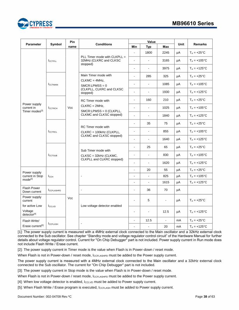
Power supply current in Timer modes[2]
ICCTPLL
Vcc
PLL Timer mode with CLKPLL = 32MHz (CLKRC and CLKSC stopped)
- 1800 2245 µA TA = +25°C
- - 3165 µA TA = +105°C
- - 3975 µA TA = +125°C
ICCTMAIN
Main Timer mode with
CLKMC = 4MHz,
SMCR:LPMSS = 0 (CLKPLL, CLKRC and CLKSC stopped)
- 285 325 µA TA = +25°C
- - 1085 µA TA = +105°C
- - 1930 µA TA = +125°C
ICCTRCH
RC Timer mode with
CLKRC = 2MHz,
SMCR:LPMSS = 0 (CLKPLL, CLKMC and CLKSC stopped)
- 160 210 µA TA = +25°C
- - 1025 µA TA = +105°C
- - 1840 µA TA = +125°C
ICCTRCL
RC Timer mode with
CLKRC = 100kHz (CLKPLL, CLKMC and CLKSC stopped)
- 35 75 µA TA = +25°C
- - 855 µA TA = +105°C
- - 1640 µA TA = +125°C
ICCTSUB
Sub Timer mode with
CLKSC = 32kHz (CLKMC, CLKPLL and CLKRC stopped)
- 25 65 µA TA = +25°C
- - 830 µA TA = +105°C
- - 1620 µA TA = +125°C
Power supply current in Stop mode[3]
ICCH
Vcc
-
- 20 55 µA TA = +25°C
- - 825 µA TA = +105°C
- - 1615 µA TA = +125°C
Flash Power Down current
ICCFLASHPD - - 36 70 µA
Power supply current
for active Low
Voltage detector[4]
ICCLVD Low voltage detector enabled
- 5 - µA TA = +25°C
- - 12.5 µA TA = +125°C
Flash Write/
Erase current[5] ICCFLASH -
- 12.5 - mA TA = +25°C
- - 20 mA TA = +125°C
[1]: The power supply current is measured with a 4MHz external clock connected to the Main oscillator and a 32kHz external clock connected to the Sub oscillator. See chapter “Standby mode and voltage regulator control circuit” of the Hardware Manual for further details about voltage regulator control. Current for "On Chip Debugger" part is not included. Power supply current in Run mode does not include Flash Write / Erase current.
[2]: The power supply current in Timer mode is the value when Flash is in Power-down / reset mode.
When Flash is not in Power-down / reset mode, ICCFLASHPD must be added to the Power supply current.
The power supply current is measured with a 4MHz external clock connected to the Main oscillator and a 32kHz external clock connected to the Sub oscillator. The current for "On Chip Debugger" part is not included.
[3]: The power supply current in Stop mode is the value when Flash is in Power-down / reset mode.
When Flash is not in Power-down / reset mode, ICCFLASHPD must be added to the Power supply current.
[4]: When low voltage detector is enabled, ICCLVD must be added to Power supply current.
[5]: When Flash Write / Erase program is executed, ICCFLASH must be added to Power supply current.
Document Number: 002-04709 Rev.*C Page 39 of 63
MB96610 Series
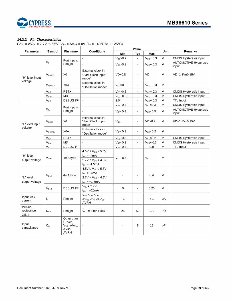
14.3.2 Pin Characteristics
(VCC = AVCC = 2.7V to 5.5V, VSS = AVSS = 0V, TA = - 40°C to + 125°C)
Parameter Symbol Pin name Conditions Value
Unit Remarks Min Typ Max
"H" level input voltage
VIH Port inputs Pnn_m
- VCC×0.7 - VCC+ 0.3 V CMOS Hysteresis input
- VCC×0.8 - VCC+ 0.3 V AUTOMOTIVE Hysteresis input
VIHX0S X0
External clock in
"Fast Clock Input mode"
VD×0.8 - VD V VD=1.8V±0.15V
VIHX0AS X0A External clock in
"Oscillation mode" VCC×0.8 - VCC+ 0.3 V
VIHR RSTX - VCC×0.8 - VCC+ 0.3 V CMOS Hysteresis input
VIHM MD - VCC- 0.3 - VCC+ 0.3 V CMOS Hysteresis input
VIHD DEBUG I/F - 2.0 - VCC+ 0.3 V TTL Input
"L" level input voltage
VIL Port inputs Pnn_m
- VSS- 0.3 - VCC×0.3 V CMOS Hysteresis input
- VSS- 0.3 - VCC×0.5 V AUTOMOTIVE Hysteresis input
VILX0S X0 External clock in "Fast Clock Input mode"
VSS - VD×0.2 V VD=1.8V±0.15V
VILX0AS X0A External clock in
"Oscillation mode" VSS- 0.3 - VCC×0.2 V
VILR RSTX - VSS- 0.3 - VCC×0.2 V CMOS Hysteresis input
VILM MD - VSS- 0.3 - VSS+ 0.3 V CMOS Hysteresis input
VILD DEBUG I/F - VSS- 0.3 - 0.8 V TTL Input
"H" level
output voltage VOH4 4mA type
4.5V ≤ VCC ≤ 5.5V
IOH = -4mA VCC- 0.5 - VCC V
2.7V ≤ VCC < 4.5V
IOH = -1.5mA
"L" level
output voltage
VOL4 4mA type
4.5V ≤ VCC ≤ 5.5V
IOL = +4mA - - 0.4 V
2.7V ≤ VCC < 4.5V
IOL = +1.7mA
VOLD DEBUG I/F VCC = 2.7V
IOL = +25mA 0 - 0.25 V
Input leak current
IIL Pnn_m
VSS < VI < VCC
AVSS < VI <AVCC, AVRH
- 1 - + 1 µA
Pull-up resistance
value
RPU Pnn_m VCC = 5.0V ±10% 25 50 100 kΩ
Input capacitance
CIN
Other than C, Vcc, Vss, AVcc, AVss, AVRH
- - 5 15 pF
Document Number: 002-04709 Rev.*C Page 40 of 63
MB96610 Series
14.4 AC Characteristics
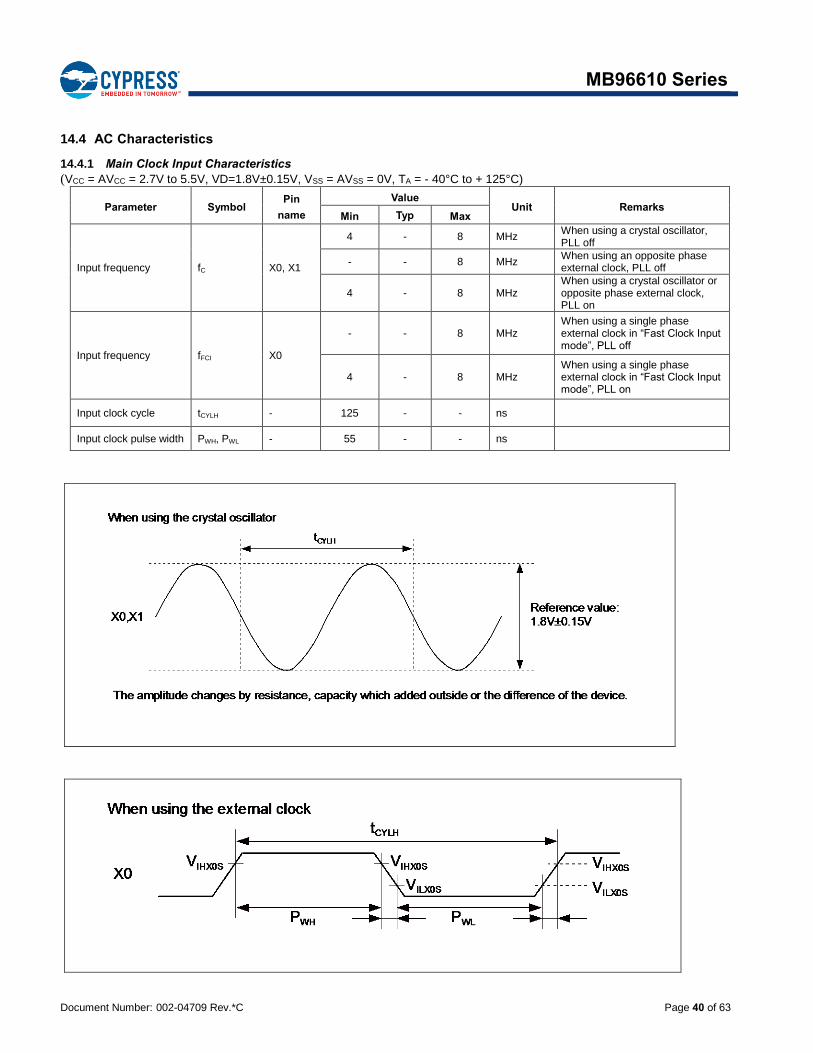
14.4.1 Main Clock Input Characteristics
(VCC = AVCC = 2.7V to 5.5V, VD=1.8V±0.15V, VSS = AVSS = 0V, TA = - 40°C to + 125°C)
Parameter Symbol Pin
name
Value Unit Remarks
Min Typ Max
Input frequency fC X0, X1
4 - 8 MHz When using a crystal oscillator, PLL off
- - 8 MHz When using an opposite phase external clock, PLL off
4 - 8 MHz When using a crystal oscillator or opposite phase external clock, PLL on
Input frequency fFCI X0
- - 8 MHz When using a single phase external clock in “Fast Clock Input mode”, PLL off
4 - 8 MHz When using a single phase external clock in “Fast Clock Input mode”, PLL on
Input clock cycle tCYLH - 125 - - ns
Input clock pulse width PWH, PWL - 55 - - ns
Document Number: 002-04709 Rev.*C Page 41 of 63
MB96610 Series
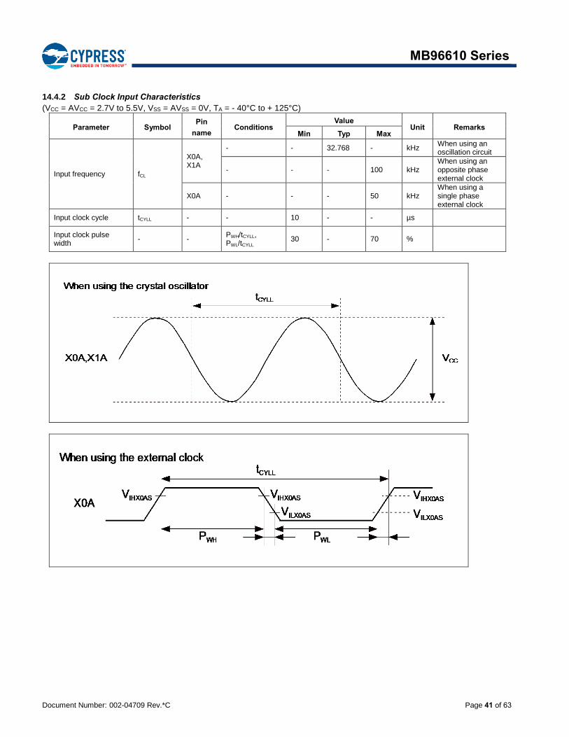
14.4.2 Sub Clock Input Characteristics
(VCC = AVCC = 2.7V to 5.5V, VSS = AVSS = 0V, TA = - 40°C to + 125°C)
Parameter Symbol Pin
name Conditions
Value Unit Remarks
Min Typ Max
Input frequency fCL
X0A, X1A
- - 32.768 - kHz When using an oscillation circuit
- - - 100 kHz When using an opposite phase external clock
X0A - - - 50 kHz When using a single phase external clock
Input clock cycle tCYLL - - 10 - - µs
Input clock pulse width
- - PWH/tCYLL, PWL/tCYLL
30 - 70 %
Document Number: 002-04709 Rev.*C Page 42 of 63
MB96610 Series
14.4.3 Built-in RC Oscillation Characteristics
(VCC = AVCC = 2.7V to 5.5V, VSS = AVSS = 0V, TA = - 40°C to + 125°C)
Parameter Symbol Value
Unit Remarks Min Typ Max
Clock frequency fRC
50 100 200 kHz When using slow frequency of RC oscillator
1 2 4 MHz When using fast frequency of RC oscillator
RC clock stabilization time tRCSTAB
80 160 320 s When using slow frequency of RC oscillator (16 RC clock cycles)
64 128 256 s
When using fast frequency of RC oscillator (256 RC clock cycles)
14.4.4 Internal Clock Timing
(VCC = AVCC = 2.7V to 5.5V, VSS = AVSS = 0V, TA = - 40°C to + 125°C)
Parameter Symbol Value
Unit Min Max
Internal System clock frequency
(CLKS1 and CLKS2) fCLKS1, fCLKS2 - 54 MHz
Internal CPU clock frequency (CLKB), Internal peripheral clock frequency (CLKP1)
fCLKB, fCLKP1 - 32 MHz
Internal peripheral clock frequency (CLKP2) fCLKP2 - 32 MHz
Document Number: 002-04709 Rev.*C Page 43 of 63
MB96610 Series
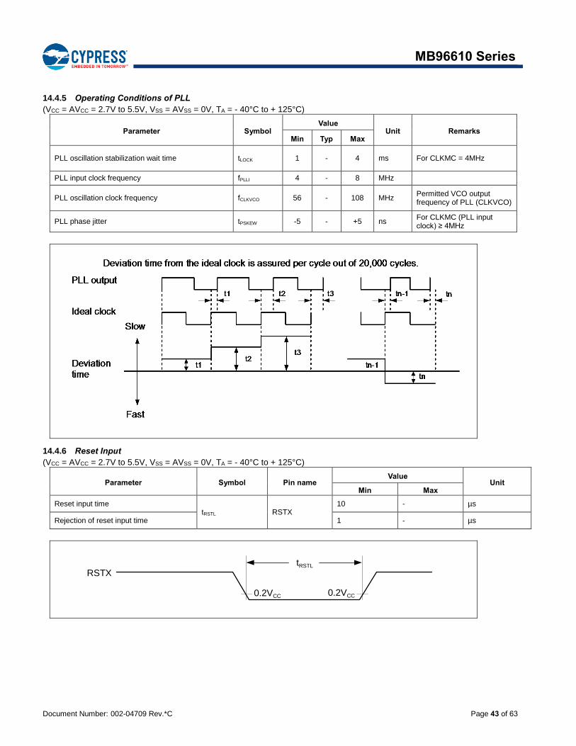
14.4.5 Operating Conditions of PLL
(VCC = AVCC = 2.7V to 5.5V, VSS = AVSS = 0V, TA = - 40°C to + 125°C)
Parameter Symbol Value
Unit Remarks Min Typ Max
PLL oscillation stabilization wait time tLOCK 1 - 4 ms For CLKMC = 4MHz
PLL input clock frequency fPLLI 4 - 8 MHz
PLL oscillation clock frequency fCLKVCO 56 - 108 MHz Permitted VCO output frequency of PLL (CLKVCO)
PLL phase jitter tPSKEW -5 - +5 ns For CLKMC (PLL input clock) ≥ 4MHz
14.4.6 Reset Input
(VCC = AVCC = 2.7V to 5.5V, VSS = AVSS = 0V, TA = - 40°C to + 125°C)
Parameter Symbol Pin name Value
Unit Min Max
Reset input time tRSTL RSTX
10 - µs
Rejection of reset input time 1 - µs
RSTX
0.2VCC 0.2VCC
tRSTL
Document Number: 002-04709 Rev.*C Page 44 of 63
MB96610 Series
14.4.7 Power-on Reset Timing
(VCC = AVCC = 2.7V to 5.5V, VSS = AVSS = 0V, TA = - 40°C to + 125°C)
Parameter Symbol Pin name Value
Unit Min Typ Max
Power on rise time tR Vcc 0.05 - 30 ms
Power off time tOFF Vcc 1 - - ms
Document Number: 002-04709 Rev.*C Page 45 of 63
MB96610 Series
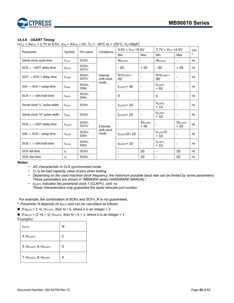
14.4.8 USART Timing
(VCC = AVCC = 2.7V to 5.5V, VSS = AVSS = 0V, TA = - 40°C to + 125°C, CL=50pF)
Parameter Symbol Pin name Conditions 4.5V VCC <5.5V 2.7V VCC <4.5V Uni
t Min Max Min Max
Serial clock cycle time tSCYC SCKn
Internal shift clock mode
4tCLKP1 - 4tCLKP1 - ns
SCK ↓ →SOT delay time tSLOVI SCKn, SOTn
- 20 + 20 - 30 + 30 ns
SOT → SCK ↑ delay time tOVSHI SCKn, SOTn
N×tCLKP1–20*
- N×tCLKP1– 30*
- ns
SIN → SCK ↑ setup time tIVSHI SCKn, SINn
tCLKP1+ 45 - tCLKP1
+ 55 - ns
SCK ↑ → SIN hold time tSHIXI SCKn, SINn
0 - 0 - ns
Serial clock "L" pulse width tSLSH SCKn
External shift clock mode
tCLKP1+ 10 - tCLKP1
+ 10 - ns
Serial clock "H" pulse width tSHSL SCKn tCLKP1+ 10 - tCLKP1
+ 10 - ns
SCK ↓ → SOT delay time tSLOVE SCKn, SOTn
- 2tCLKP1
+ 45 -
2tCLKP1
+ 55 ns
SIN → SCK ↑ setup time tIVSHE SCKn, SINn
tCLKP1/2+ 10 - tCLKP1/2 + 10
- ns
SCK ↑ → SIN hold time tSHIXE SCKn, SINn
tCLKP1+ 10 - tCLKP1
+ 10 - ns
SCK fall time tF SCKn - 20 - 20 ns
SCK rise time tR SCKn - 20 - 20 ns
Notes:
− AC characteristic in CLK synchronized mode
− CL is he load capacity value of pins when testing.
− Depending on the used machine clock frequency, the maximum possible baud rate can be limited by some parameters. These parameters are shown in “MB96600 series HARDWARE MANUAL”.
− tCLKP1 indicates the peripheral clock 1 (CLKP1), Unit: ns These characteristics only guarantee the same relocate port number.
For example, the combination of SCKn and SOTn_R is not guaranteed.
*: Parameter N depends on tSCYC and can be calculated as follows:
If tSCYC = 2 ×k ×tCLKP1, then N = k, where k is an integer > 2
If tSCYC = (2 ×k + 1) ×tCLKP1, then N = k + 1, where k is an integer > 1
Examples:
tSCYC N
4 ×tCLKP1 2
5 ×tCLKP1, 6 ×tCLKP1 3
7 ×tCLKP1, 8 ×tCLKP1 4
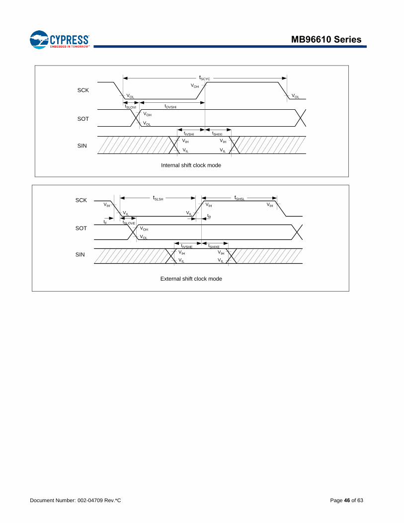
Document Number: 002-04709 Rev.*C Page 46 of 63
MB96610 Series
tSCYC
VOL VOL
VOH
VOH
VIH VIH
VILVIL
tSLOVI
tIVSHI tSHIXI
VOL
SCK
SOT
SIN
Internal shift clock mode
tOVSHI
tSLSH
VIH VIH
VIH
VIH
VIL
VIH
VIL
VIL VIL
VOL
VOH
tSLOVE
tR
tSHIXEtIVSHE
tF
SCK
SOT
SIN
tSHSL
External shift clock mode
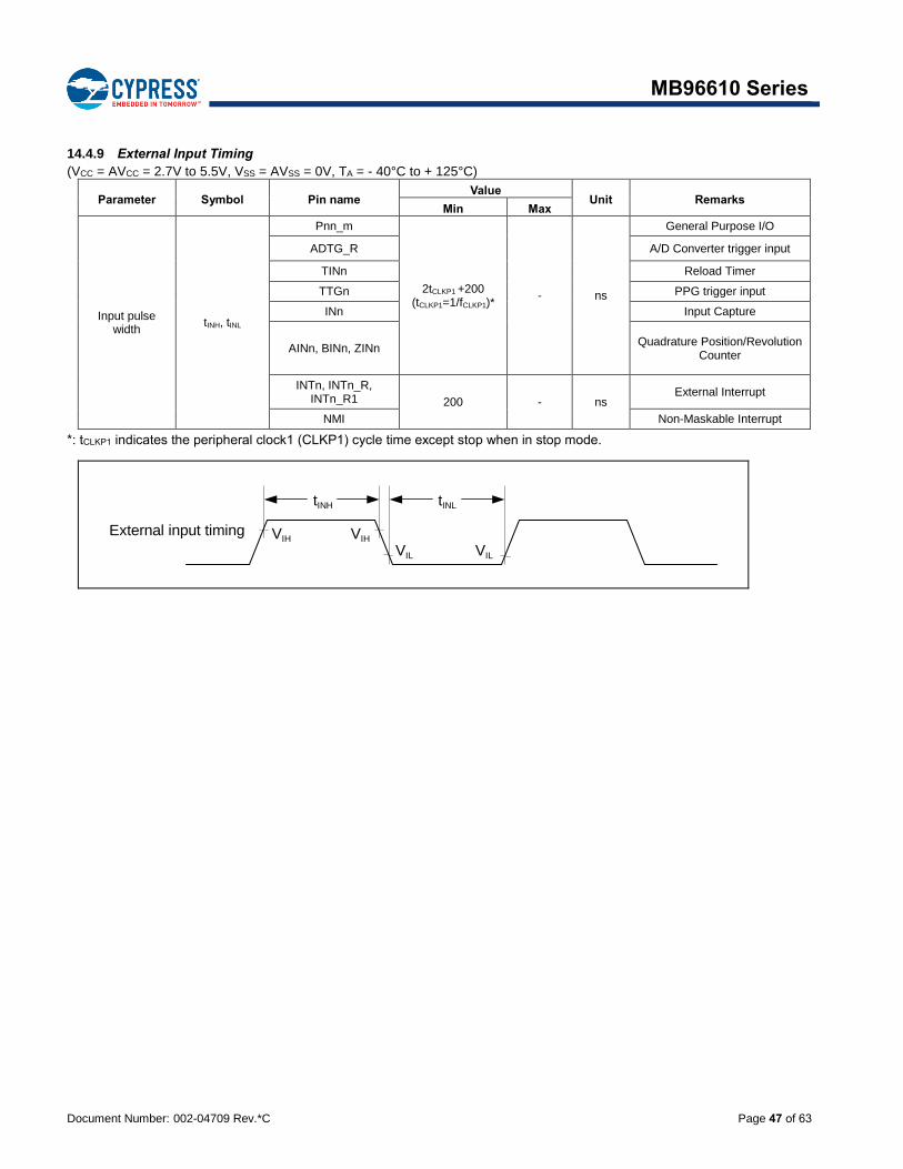
Document Number: 002-04709 Rev.*C Page 47 of 63
MB96610 Series
14.4.9 External Input Timing
(VCC = AVCC = 2.7V to 5.5V, VSS = AVSS = 0V, TA = - 40°C to + 125°C)
Parameter Symbol Pin name Value
Unit Remarks Min Max
Input pulse width
tINH, tINL
Pnn_m
2tCLKP1 +200 (tCLKP1=1/fCLKP1)*
- ns
General Purpose I/O
ADTG_R A/D Converter trigger input
TINn Reload Timer
TTGn PPG trigger input
INn Input Capture
AINn, BINn, ZINn Quadrature Position/Revolution
Counter
INTn, INTn_R, INTn_R1 200 - ns
External Interrupt
NMI Non-Maskable Interrupt
*: tCLKP1 indicates the peripheral clock1 (CLKP1) cycle time except stop when in stop mode.
VIH
VIL
tINLtINH
VIL
External input timing VIH
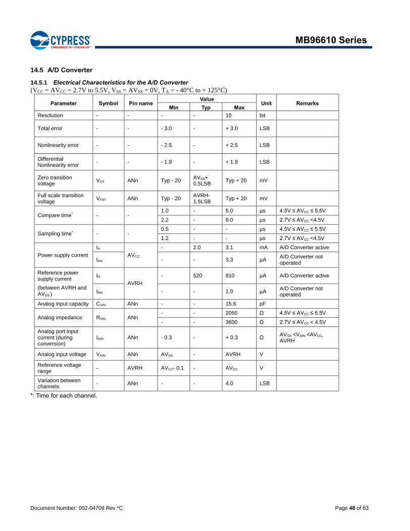
Document Number: 002-04709 Rev.*C Page 48 of 63
MB96610 Series
14.5 A/D Converter
14.5.1 Electrical Characteristics for the A/D Converter
(VCC = AVCC = 2.7V to 5.5V, VSS = AVSS = 0V, TA = - 40°C to + 125°C)
Parameter Symbol Pin name Value
Unit Remarks Min Typ Max
Resolution - - - - 10 bit
Total error - - - 3.0 - + 3.0 LSB
Nonlinearity error - - - 2.5 - + 2.5 LSB
Differential Nonlinearity error
- - - 1.9 - + 1.9 LSB
Zero transition voltage
VOT ANn Typ - 20 AVSS+ 0.5LSB
Typ + 20 mV
Full scale transition voltage
VFST ANn Typ - 20 AVRH- 1.5LSB
Typ + 20 mV
Compare time* - - 1.0 - 5.0 µs 4.5V ≤ ΑVCC ≤ 5.5V
2.2 - 8.0 µs 2.7V ≤ ΑVCC <4.5V
Sampling time* - - 0.5 - - µs 4.5V ≤ ΑVCC ≤ 5.5V
1.2 - - µs 2.7V ≤ ΑVCC <4.5V
Power supply current
IA
AVCC
- 2.0 3.1 mA A/D Converter active
IAH - - 3.3 µA A/D Converter not operated
Reference power supply current
(between AVRH and AVSS )
IR
AVRH
- 520 810 µA A/D Converter active
IRH - - 1.0 µA A/D Converter not operated
Analog input capacity CVIN ANn - - 15.6 pF
Analog impedance RVIN ANn - - 2050 Ω 4.5V ≤ AVCC ≤ 5.5V
- - 3600 Ω 2.7V ≤ AVCC < 4.5V
Analog port input current (during conversion)
IAIN ANn - 0.3 - + 0.3 Ω AVSS <VAIN <AVCC, AVRH
Analog input voltage VAIN ANn AVSS - AVRH V
Reference voltage range
- AVRH AVCC- 0.1 - AVCC V
Variation between channels
- ANn - - 4.0 LSB
*: Time for each channel.
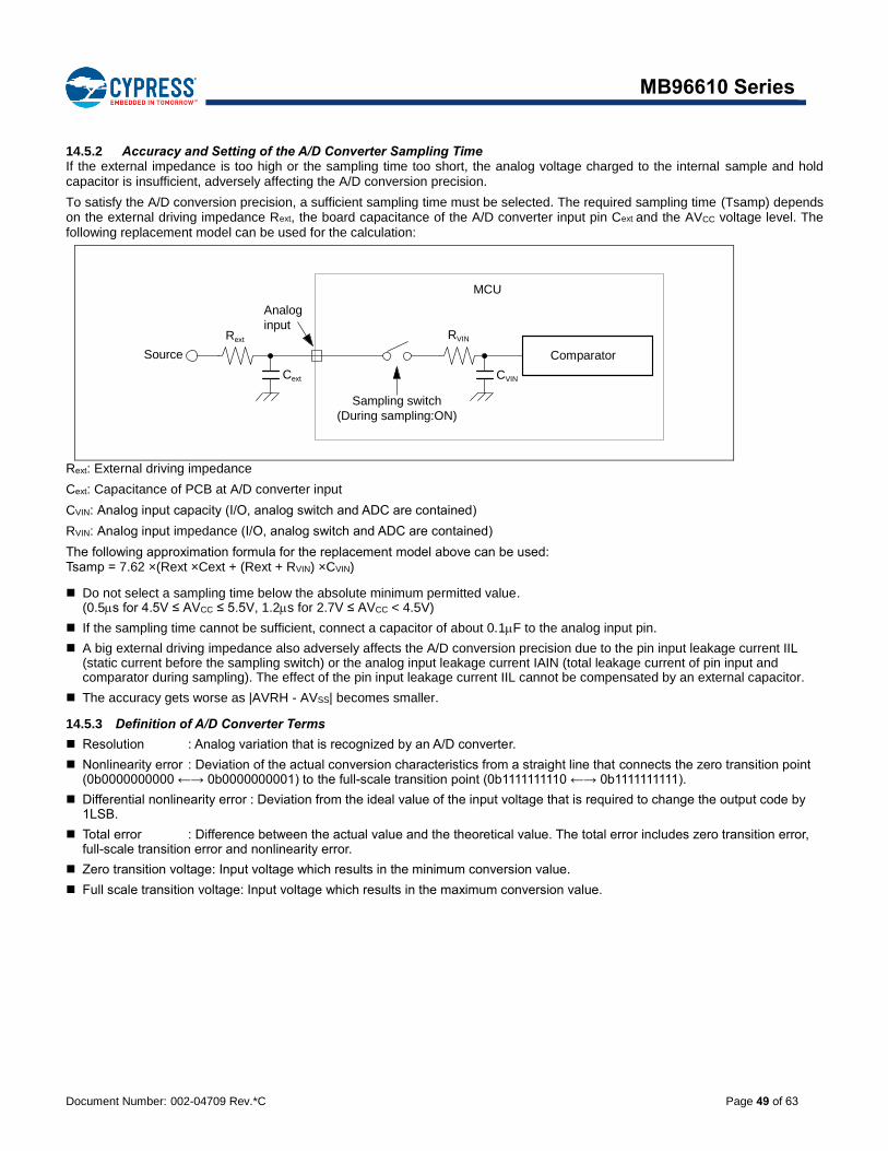
Document Number: 002-04709 Rev.*C Page 49 of 63
MB96610 Series
14.5.2 Accuracy and Setting of the A/D Converter Sampling Time If the external impedance is too high or the sampling time too short, the analog voltage charged to the internal sample and hold capacitor is insufficient, adversely affecting the A/D conversion precision.
To satisfy the A/D conversion precision, a sufficient sampling time must be selected. The required sampling time (Tsamp) depends on the external driving impedance Rext, the board capacitance of the A/D converter input pin Cext and the AVCC voltage level. The following replacement model can be used for the calculation:
Rext: External driving impedance
Cext: Capacitance of PCB at A/D converter input
CVIN: Analog input capacity (I/O, analog switch and ADC are contained)
RVIN: Analog input impedance (I/O, analog switch and ADC are contained)
The following approximation formula for the replacement model above can be used: Tsamp = 7.62 ×(Rext ×Cext + (Rext + RVIN) ×CVIN)
Do not select a sampling time below the absolute minimum permitted value. (0.5s for 4.5V ≤ AVCC ≤ 5.5V, 1.2s for 2.7V ≤ AVCC < 4.5V)
If the sampling time cannot be sufficient, connect a capacitor of about 0.1F to the analog input pin.
A big external driving impedance also adversely affects the A/D conversion precision due to the pin input leakage current IIL (static current before the sampling switch) or the analog input leakage current IAIN (total leakage current of pin input and comparator during sampling). The effect of the pin input leakage current IIL cannot be compensated by an external capacitor.
The accuracy gets worse as |AVRH - AVSS| becomes smaller.
14.5.3 Definition of A/D Converter Terms
Resolution : Analog variation that is recognized by an A/D converter.
Nonlinearity error : Deviation of the actual conversion characteristics from a straight line that connects the zero transition point (0b0000000000 ←→ 0b0000000001) to the full-scale transition point (0b1111111110 ←→ 0b1111111111).
Differential nonlinearity error : Deviation from the ideal value of the input voltage that is required to change the output code by 1LSB.
Total error : Difference between the actual value and the theoretical value. The total error includes zero transition error, full-scale transition error and nonlinearity error.
Zero transition voltage: Input voltage which results in the minimum conversion value.
Full scale transition voltage: Input voltage which results in the maximum conversion value.
Sampling switch
(During sampling:ON)
CVIN
RVIN
Analog
input
MCU
Rext
Cext
Source Comparator
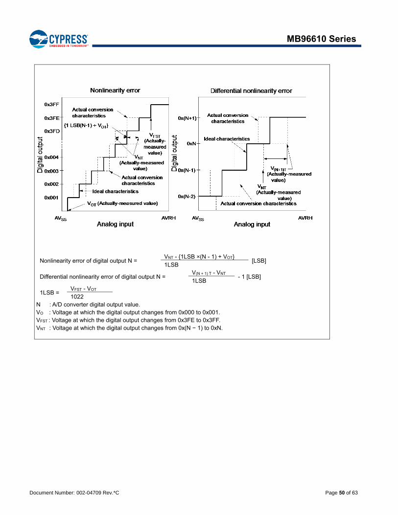
Document Number: 002-04709 Rev.*C Page 50 of 63
MB96610 Series
Nonlinearity error of digital output N = VNT - {1LSB ×(N - 1) + VOT}
[LSB] 1LSB
Differential nonlinearity error of digital output N = V(N + 1) T - VNT
- 1 [LSB] 1LSB
1LSB = VFST - VOT
1022
N : A/D converter digital output value.
VO : Voltage at which the digital output changes from 0x000 to 0x001.
VFST : Voltage at which the digital output changes from 0x3FE to 0x3FF.
VNT : Voltage at which the digital output changes from 0x(N − 1) to 0xN.
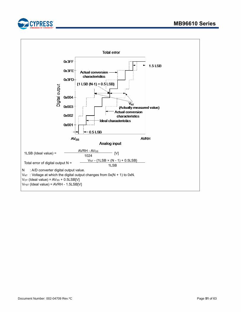
Document Number: 002-04709 Rev.*C Page 51 of 63
MB96610 Series
1LSB (Ideal value) = AVRH - AVSS
[V] 1024
Total error of digital output N = VNT - {1LSB × (N - 1) + 0.5LSB}
1LSB
N : A/D converter digital output value.
VNT : Voltage at which the digital output changes from 0x(N + 1) to 0xN.
VOT (Ideal value) = AVSS + 0.5LSB[V]
VFST (Ideal value) = AVRH - 1.5LSB[V]
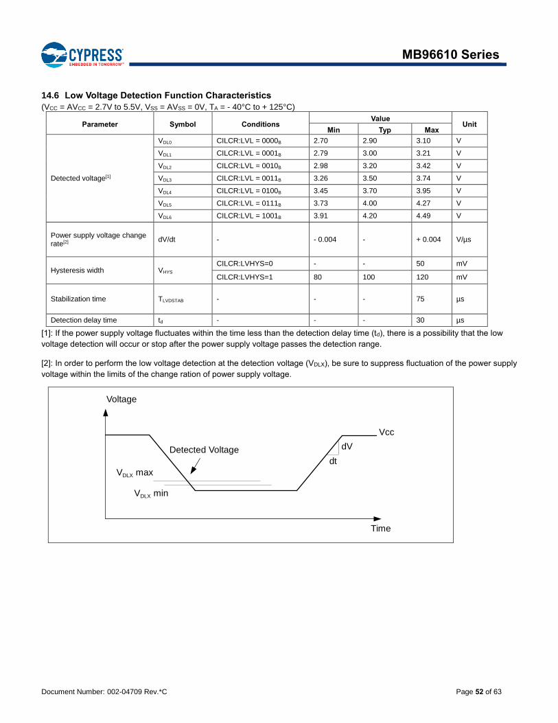
Document Number: 002-04709 Rev.*C Page 52 of 63
MB96610 Series
14.6 Low Voltage Detection Function Characteristics
(VCC = AVCC = 2.7V to 5.5V, VSS = AVSS = 0V, TA = - 40°C to + 125°C)
Parameter Symbol Conditions Value
Unit Min Typ Max
Detected voltage[1]
VDL0 CILCR:LVL = 0000B 2.70 2.90 3.10 V
VDL1 CILCR:LVL = 0001B 2.79 3.00 3.21 V
VDL2 CILCR:LVL = 0010B 2.98 3.20 3.42 V
VDL3 CILCR:LVL = 0011B 3.26 3.50 3.74 V
VDL4 CILCR:LVL = 0100B 3.45 3.70 3.95 V
VDL5 CILCR:LVL = 0111B 3.73 4.00 4.27 V
VDL6 CILCR:LVL = 1001B 3.91 4.20 4.49 V
Power supply voltage change rate[2]
dV/dt - - 0.004 - + 0.004 V/µs
Hysteresis width VHYS CILCR:LVHYS=0 - - 50 mV
CILCR:LVHYS=1 80 100 120 mV
Stabilization time TLVDSTAB - - - 75 µs
Detection delay time td - - - 30 µs
[1]: If the power supply voltage fluctuates within the time less than the detection delay time (td), there is a possibility that the low
voltage detection will occur or stop after the power supply voltage passes the detection range.
[2]: In order to perform the low voltage detection at the detection voltage (VDLX), be sure to suppress fluctuation of the power supply
voltage within the limits of the change ration of power supply voltage.
Time
Vcc
VDLX min
Voltage
VDLX max
dV
dt
Detected Voltage
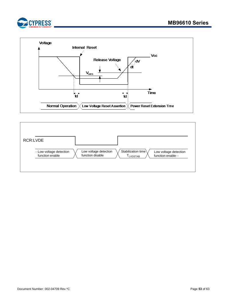
Document Number: 002-04709 Rev.*C Page 53 of 63
MB96610 Series
RCR:LVDE
···Low voltage detection
function enable
Low voltage detection
function disable
Stabilization time
TLVDSTAB
Low voltage detection
function enable···
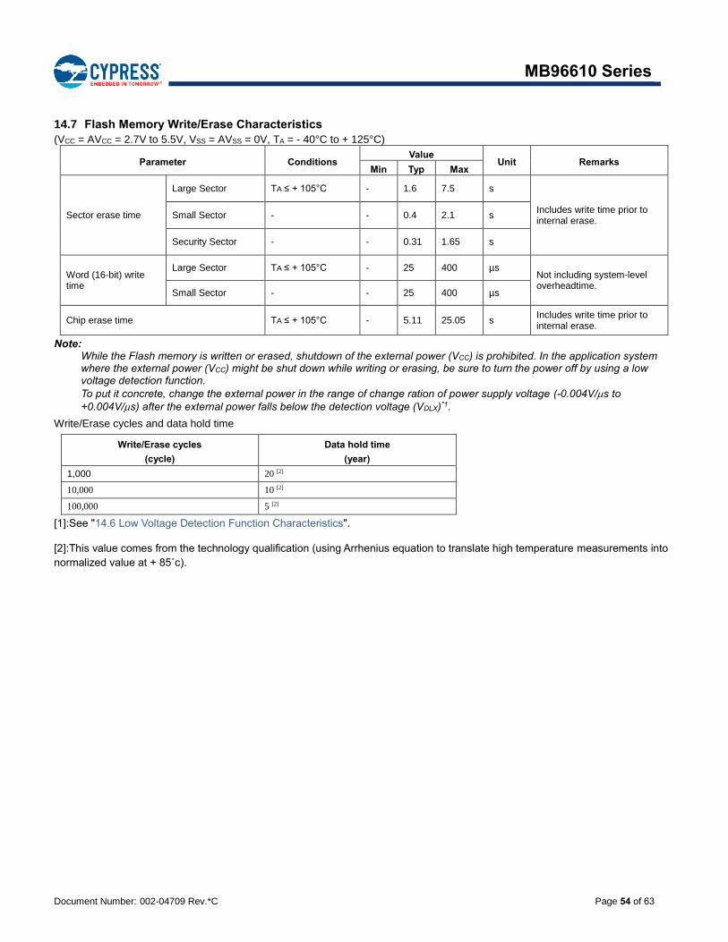
Document Number: 002-04709 Rev.*C Page 54 of 63
MB96610 Series
14.7 Flash Memory Write/Erase Characteristics
(VCC = AVCC = 2.7V to 5.5V, VSS = AVSS = 0V, TA = - 40°C to + 125°C)
Parameter Conditions Value
Unit Remarks Min Typ Max
Sector erase time
Large Sector TA ≤ + 105°C - 1.6 7.5 s
Includes write time prior to internal erase.
Small Sector - - 0.4 2.1 s
Security Sector - - 0.31 1.65 s
Word (16-bit) write time
Large Sector TA ≤ + 105°C - 25 400 µs Not including system-level overheadtime.
Small Sector - - 25 400 µs
Chip erase time TA ≤ + 105°C - 5.11 25.05 s Includes write time prior to internal erase.
Note: While the Flash memory is written or erased, shutdown of the external power (VCC) is prohibited. In the application system where the external power (VCC) might be shut down while writing or erasing, be sure to turn the power off by using a low voltage detection function.
To put it concrete, change the external power in the range of change ration of power supply voltage (-0.004V/s to
+0.004V/s) after the external power falls below the detection voltage (VDLX)*1.
Write/Erase cycles and data hold time
Write/Erase cycles
(cycle)
Data hold time
(year)
1,000 20 [2]
10,000 10 [2]
100,000 5 [2]
[1]:See "14.6 Low Voltage Detection Function Characteristics".
[2]:This value comes from the technology qualification (using Arrhenius equation to translate high temperature measurements into
normalized value at + 85˚c).
Document Number: 002-04709 Rev.*C Page 55 of 63
MB96610 Series
15. Example Characteristics
This characteristic is an actual value of the arbitrary sample. It is not the guaranteed value.
MB96F615
0.01
0.10
1.00
10.00
100.00
-50 0 50 100 150
I CC
[mA
]
TA [ºC]
Run Mode
PLL clock (32MHz)
Main osc. (4MHz)
RC clock (2MHz)
RC clock (100kHz)
Sub osc. (32kHz)
(VCC = 5.5V)
0.001
0.010
0.100
1.000
10.000
100.000
-50 0 50 100 150
I CC
[mA
]
TA [ºC]
Sleep Mode
PLL clock (32MHz)
Main osc. (4MHz)
RC clock (2MHz)
RC clock (100kHz)
Sub osc. (32kHz)
(VCC = 5.5V)
Document Number: 002-04709 Rev.*C Page 56 of 63
MB96610 Series
MB96F615
0.001
0.010
0.100
1.000
10.000
-50 0 50 100 150
I CC
[mA
]
TA [ºC]
Timer Mode
PLL clock (32MHz)
Main osc. (4MHz)
RC clock (2MHz)
RC clock (100kHz)
Sub osc. (32kHz)
(VCC = 5.5V)
0.001
0.010
0.100
1.000
-50 0 50 100 150
I CC
[mA
]
TA [ºC]
Stop Mode (VCC = 5.5V)
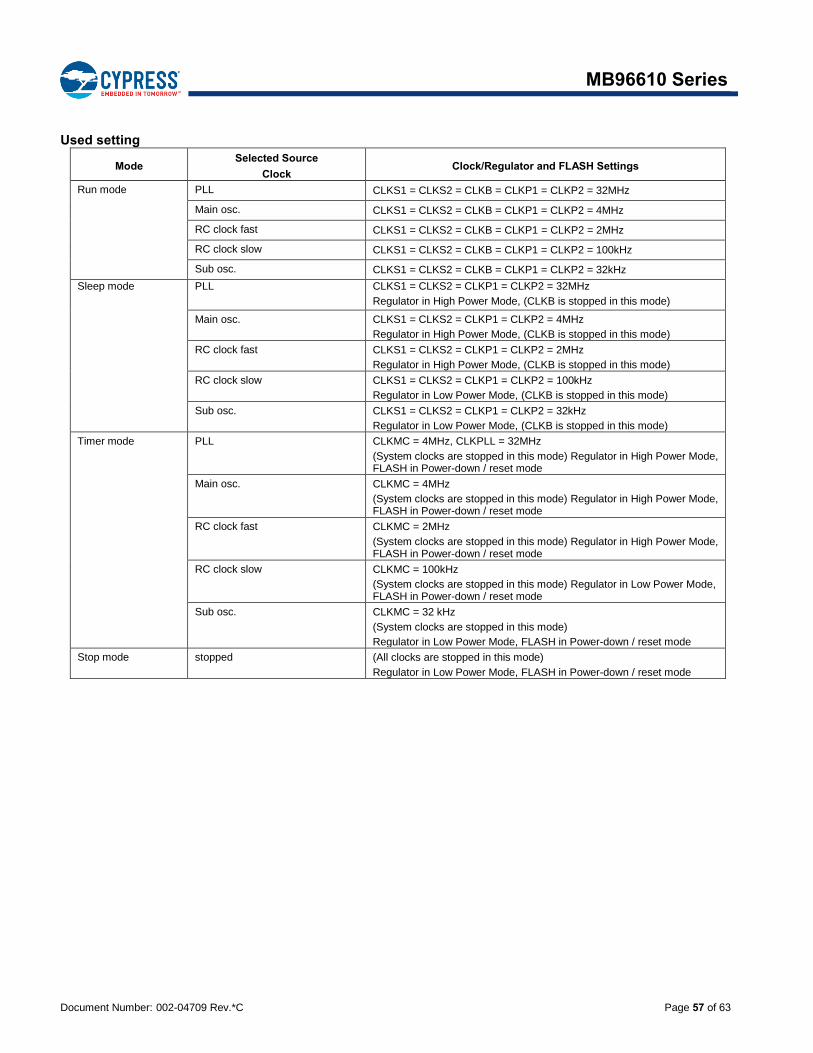
Document Number: 002-04709 Rev.*C Page 57 of 63
MB96610 Series
Used setting
Mode Selected Source
Clock Clock/Regulator and FLASH Settings
Run mode PLL CLKS1 = CLKS2 = CLKB = CLKP1 = CLKP2 = 32MHz
Main osc. CLKS1 = CLKS2 = CLKB = CLKP1 = CLKP2 = 4MHz
RC clock fast CLKS1 = CLKS2 = CLKB = CLKP1 = CLKP2 = 2MHz
RC clock slow CLKS1 = CLKS2 = CLKB = CLKP1 = CLKP2 = 100kHz
Sub osc. CLKS1 = CLKS2 = CLKB = CLKP1 = CLKP2 = 32kHz
Sleep mode PLL CLKS1 = CLKS2 = CLKP1 = CLKP2 = 32MHz
Regulator in High Power Mode, (CLKB is stopped in this mode)
Main osc. CLKS1 = CLKS2 = CLKP1 = CLKP2 = 4MHz
Regulator in High Power Mode, (CLKB is stopped in this mode)
RC clock fast CLKS1 = CLKS2 = CLKP1 = CLKP2 = 2MHz
Regulator in High Power Mode, (CLKB is stopped in this mode)
RC clock slow CLKS1 = CLKS2 = CLKP1 = CLKP2 = 100kHz
Regulator in Low Power Mode, (CLKB is stopped in this mode)
Sub osc. CLKS1 = CLKS2 = CLKP1 = CLKP2 = 32kHz
Regulator in Low Power Mode, (CLKB is stopped in this mode)
Timer mode PLL CLKMC = 4MHz, CLKPLL = 32MHz
(System clocks are stopped in this mode) Regulator in High Power Mode, FLASH in Power-down / reset mode
Main osc. CLKMC = 4MHz
(System clocks are stopped in this mode) Regulator in High Power Mode, FLASH in Power-down / reset mode
RC clock fast CLKMC = 2MHz
(System clocks are stopped in this mode) Regulator in High Power Mode, FLASH in Power-down / reset mode
RC clock slow CLKMC = 100kHz
(System clocks are stopped in this mode) Regulator in Low Power Mode, FLASH in Power-down / reset mode
Sub osc. CLKMC = 32 kHz
(System clocks are stopped in this mode)
Regulator in Low Power Mode, FLASH in Power-down / reset mode
Stop mode stopped (All clocks are stopped in this mode)
Regulator in Low Power Mode, FLASH in Power-down / reset mode

Document Number: 002-04709 Rev.*C Page 58 of 63
MB96610 Series
16. Ordering Information
MCU with CAN controller
Part number Flash memory Package*
MB96F612RBPMC-GSE1
Flash A (64.5KB) 48-pin plastic LQFP (LQA048)
MB96F612RBPMC-GS-UJE1
MB96F612RBPMC-GSE2
MB96F612RBPMC-GS-UJE2
MB96F612RBPMC-GTE1
MB96F613RBPMC-GSE1
Flash A (96.5KB) 48-pin plastic LQFP (LQA048)
MB96F613RBPMC-GS-UJE1
MB96F613RBPMC-GSE2
MB96F613RBPMC-GS-UJE2
MB96F613RBPMC-GTE1
MB96F615RBPMC-GSE1
Flash A (160.5KB) 48-pin plastic LQFP (LQA048)
MB96F615RBPMC-GS-UJE1
MB96F615RBPMC-GSE2
MB96F615RBPMC-GS-UJE2
MB96F615RBPMC-GTE1
*: For details about package, see "Package Dimension".
MCU without CAN controller
Part number Flash memory Package*
MB96F612ABPMC-GSE1
Flash A (64.5KB)
48-pin plastic LQFP (LQA048)
MB96F612ABPMC-GS-UJE1
MB96F612ABPMC-GSE2
MB96F612ABPMC-GS-UJE2
MB96F612ABPMC-GTE1
MB96F613ABPMC-GSE1
Flash A (96.5KB)
48-pin plastic LQFP (LQA048)
MB96F613ABPMC-GS-UJE1
MB96F613ABPMC-GSE2
MB96F613ABPMC-GS-UJE2
MB96F613ABPMC-GTE1
MB96F615ABPMC-GSE1
Flash A (160.5KB)
48-pin plastic LQFP (LQA048) MB96F615ABPMC-GS-UJE1
MB96F615ABPMC-GSE2
MB96F615ABPMC-GTE1
*: For details about package, see "Package Dimension".
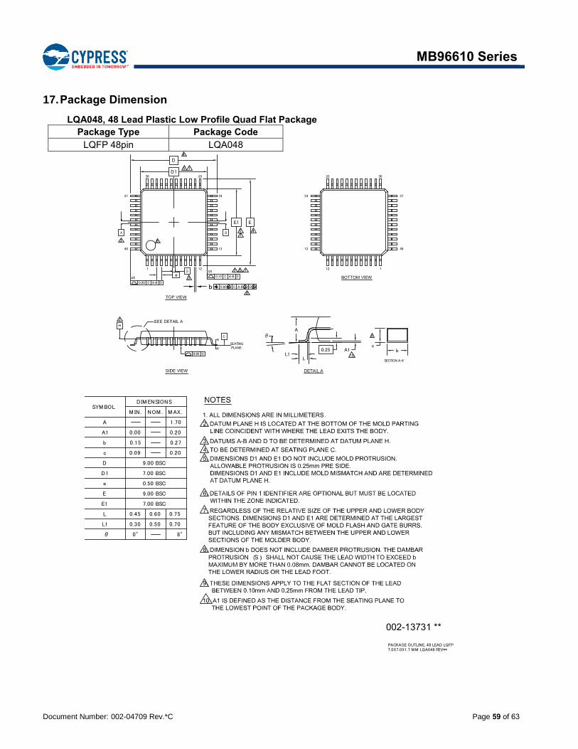
Document Number: 002-04709 Rev.*C Page 59 of 63
MB96610 Series
17. Package Dimension
LQA048, 48 Lead Plastic Low Profile Quad Flat Package
Package Type Package Code
LQFP 48pin LQA048
DIM ENSIONSSYM BOL
M IN. NOM . M AX.
A 1.70
A1 0.00 0.20
b 0.15 0.27
c 0.09 0.20
D 9.00 BSC
D1 7.00 BSC
e 0.50 BSC
E
E1
L 0.45 0.60 0.75
L1 0.30 0.50 0.70
9.00 BSC
7.00 BSC
0° 8°θ
D1
D
e
1 12
48
EE1
457
4
5 7
3
0.20 C A-B D
3
b
0.10 C A-B D
0.80 C A-B D
8
752
2
A
A'
SEATINGPLANE
θA
A10.2510
b
SECTION A-A'
c
9
L1L
6
0.80 C
1
4813
24
36 25
37
12
13
24
25 36
37
7.0X7.0X1.7 MM LQA048 REV**PACKAGE OUTLINE, 48 LEAD LQFP
002-13731 **
Document Number: 002-04709 Rev.*C Page 60 of 63
MB96610 Series
18. Major Changes
Spansion Publication Number: MB96610_DS704-00007
Page Section Change Results
Revision 3.0
4
FEATURES Changed the description of “External Interrupts”
Interrupt mask and pending bit per channel
Interrupt mask bit per channel
23 to 26 HANDLING PRECAUTIONS Added a section
34
ELECTRICAL CHARACTERISTICS
3. DC Characteristics
(1) Current Rating
Changed the Conditions for ICCSRCH
CLKS1/2 = CLKB = CLKP1/2 = CLKRC = 2MHz,
CLKS1/2 = CLKP1/2 = CLKRC = 2MHz,
Changed the Conditions for ICCSRCL
CLKS1/2 = CLKB = CLKP1/2 = CLKRC = 100kHz
CLKS1/2 = CLKP1/2 = CLKRC = 100kHz
35
Changed the Conditions for ICCTPLL
PLL Timer mode with CLKP1 = 32MHz
PLL Timer mode with CLKPLL = 32MHz
Changed the Value of “Power supply current in Timer modes”
ICCTPLL
Typ: 2480μA → 1800μA (TA = +25°C)
Max: 2710μA → 2245μA (TA = +25°C)
Max: 3985μA → 3165μA (TA = +105°C)
Max: 4830μA → 3975μA (TA = +125°C)
Changed the Conditions for ICCTRCL
RC Timer mode with CLKRC = 100kHz,
SMCR:LPMSS = 0 (CLKPLL, CLKMC and CLKSC stopped)
RC Timer mode with CLKRC = 100kHz
(CLKPLL, CLKMC and CLKSC stopped)
36
Changed the annotation *2
Power supply for "On Chip Debugger" part is not included.
Power supply current in Run mode does not include
Flash Write / Erase current.
The current for "On Chip Debugger" part is not included.
47 5. A/D Converter (2) Accuracy and Setting of the A/D Converter Sampling Time
Deleted the unit “[Min]” from approximation formula of Sampling time
52
7. Flash Memory Write/Erase Characteristics Changed the condition
(VCC = AVCC = 2.7V to 5.5V, VD=1.8V±0.15V, VSS = AVSS = 0V, TA = - 40°C to + 125°C)
(VCC = AVCC = 2.7V to 5.5V, VSS = AVSS = 0V, TA = - 40°C to + 125°C)
Document Number: 002-04709 Rev.*C Page 61 of 63
MB96610 Series
Page Section Change Results
52
ELECTRICAL CHARACTERISTICS
7. Flash Memory Write/Erase Characteristics
Changed the Note
While the Flash memory is written or erased, shutdown of the external power (VCC) is prohibited. In the application system where the external power (VCC) might be shut down while writing, be sure to turn the power off by using an external voltage detector.
While the Flash memory is written or erased, shutdown of the external power (VCC) is prohibited. In the application system where the external power (VCC) might be shut down while writing or erasing, be sure to turn the power off by using a low voltage detection function.
56
ORDERING INFORMATION
Deleted the Part number
MCU with CAN controller
MB96F612RBPMC-GTE2
MB96F613RBPMC-GTE2
MB96F615RBPMC-GTE2
MCU without CAN controller
MB96F612ABPMC-GTE2
MB96F613ABPMC-GTE2
MB96F615ABPMC-GTE2
Revision 3.1
- - Company name and layout design change
Rev.*B
6, 8, 58, 59
1. Product Lineup
3. Pin Assignment
16. Ordering Information
17. Package Dimension
Package description modified to JEDEC description.
FPT-48P-M26 → LQA048
58 16. Ordering Information
Added the following part number.
MB96F612RBPMC-GS-UJE1,
MB96F612RBPMC-GS-UJE2,
MB96F613RBPMC-GS-UJE1,
MB96F613RBPMC-GS-UJE2,
MB96F615RBPMC-GS-UJE1,
MB96F615RBPMC-GS-UJE2,
MB96F612ABPMC-GS-UJE1,
MB96F612ABPMC-GS-UJE2
MB96F613ABPMC-GS-UJE1,
MB96F613ABPMC-GS-UJE2
MB96F615ABPMC-GS-UJE1,
MB96F615ABPMC-GS-UJE2
Rev.*C
58 16. Ordering Information Deleted the Part number
MCU without CAN controller
MB96F615ABPMC-GS-UJE2
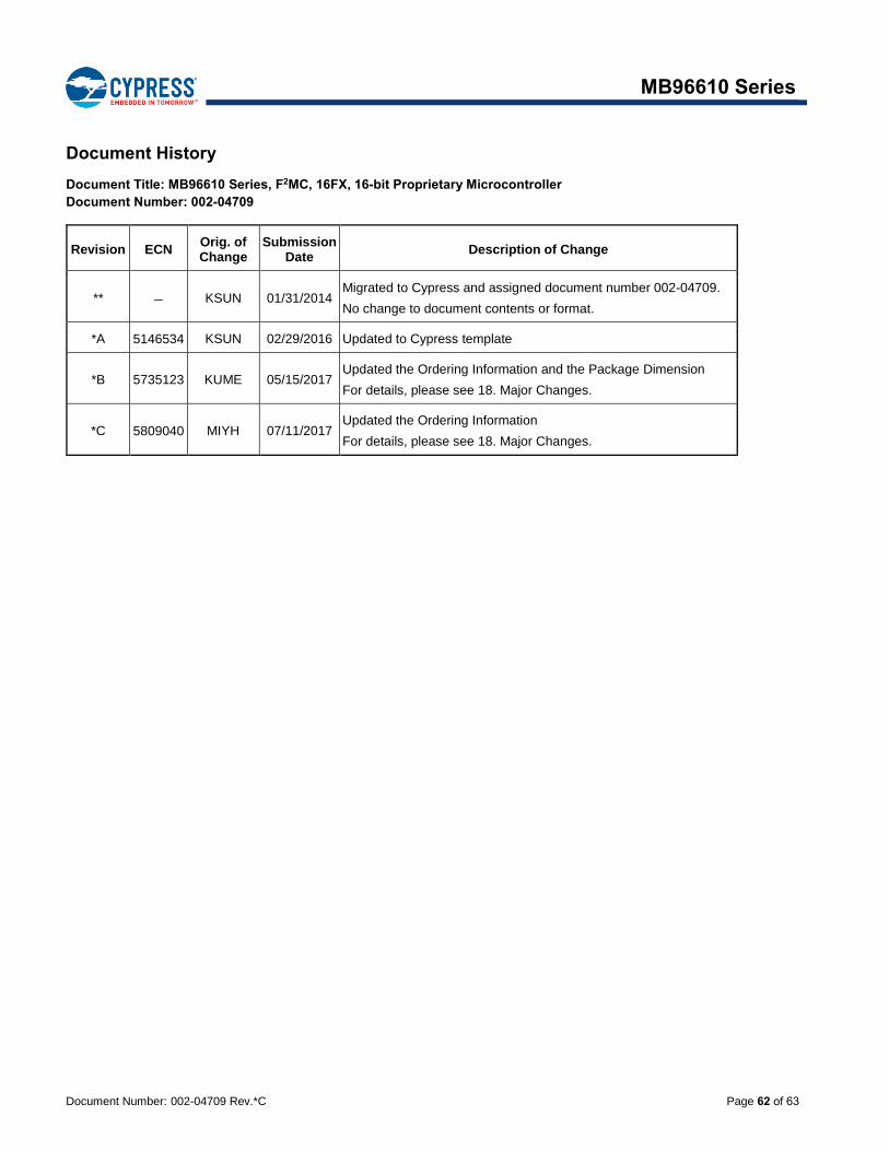
Document Number: 002-04709 Rev.*C Page 62 of 63
MB96610 Series
Document History
Document Title: MB96610 Series, F2MC, 16FX, 16-bit Proprietary Microcontroller
Document Number: 002-04709
Revision ECN Orig. of Change
Submission Date
Description of Change
** KSUN 01/31/2014 Migrated to Cypress and assigned document number 002-04709.
No change to document contents or format.
*A 5146534 KSUN 02/29/2016 Updated to Cypress template
*B 5735123 KUME 05/15/2017 Updated the Ordering Information and the Package Dimension
For details, please see 18. Major Changes.
*C 5809040 MIYH 07/11/2017 Updated the Ordering Information
For details, please see 18. Major Changes.
Document Number: 002-04709 Rev.*C Revised July 11, 2017 Page 63 of 63
MB96610 Series
Sales, Solutions, and Legal Information
Worldwide Sales and Design Support
Cypress maintains a worldwide network of offices, solution centers, manufacturer’s representatives, and distributors. To find the
office closest to you, visit us at Cypress Locations.
Products ARM® Cortex® Microcontrollers cypress.com/arm
Automotive cypress.com/automotive
Clocks & Buffers cypress.com/clocks
Interface cypress.com/interface
Internet of Things cypress.com/iot
Memory cypress.com/memory
Microcontrollers cypress.com/mcu
PSoC cypress.com/psoc
Power Management ICs cypress.com/pmic
Touch Sensing cypress.com/touch
USB Controllers cypress.com/usb
Wireless/RF cypress.com/wireless
PSoC® Solutions PSoC 1 | PSoC 3 | PSoC 4 | PSoC 5LP | PSoC 6
Cypress Developer Community Forums | WICED IOT Forums | Projects | Video | Blogs | Training | Components
Technical Support cypress.com/support
All other trademarks or registered trademarks referenced herein are the property of their respective owners.
© Cypress Semiconductor Corporation, 2014-2017. This document is the property of Cypress Semiconductor Corporation and its subsidiaries, including Spansion LLC (“Cypress”). This document,
including any software or firmware included or referenced in this document (“Software”), is owned by Cypress under the intellectual property laws and treaties of the United States and other countries worldwide. Cypress reserves all rights under such laws and treaties and does not, except as specifically stated in this paragraph, grant any license under its patents, copyrights, trademarks, or other intellectual property rights. If the Software is not accompanied by a license agreement and you do not otherwise have a writ ten agreement with Cypress governing the use of the Software, then
Cypress hereby grants you a personal, non-exclusive, nontransferable license (without the right to sublicense) (1) under its copyright rights in the Software (a) for Software provided in source code form, to modify and reproduce the Software solely for use with Cypress hardware products, only internally within your organization, and (b) to distribute the Software in binary code form externally to end users (either directly or indirectly through resellers and distributors), solely for use on Cypress hardware product units, and (2) under those claims of Cypress’s patents that are infringed by the
Software (as provided by Cypress, unmodified) to make, use, distribute, and import the Software solely for use with Cypress hardware products. Any other use, reproduction, modification, translation, or compilation of the Software is prohibited.
TO THE EXTENT PERMITTED BY APPLICABLE LAW, CYPRESS MAKES NO WARRANTY OF ANY KIND, EXPRESS OR IMPLIED, WITH REGARD TO THIS DOCUMENT OR ANY SOFTWARE
OR ACCOMPANYING HARDWARE, INCLUDING, BUT NOT LIMITED TO, THE IMPLIED WARRANTIES OF MERCHANTABILITY AND FITNESS FOR A PARTICULAR PURPOSE. To the extent permitted by applicable law, Cypress reserves the right to make changes to this document without further notice. Cypress does not assume any liability arising out of the application or use of any product or circuit described in this document. Any information provided in this document, including any sample design information or programming code, is provided only for reference purposes. It
is the responsibility of the user of this document to properly design, program, and test the functionality and safety of any application made of this information and any resulting product. Cypress products are not designed, intended, or authorized for use as critical components in systems designed or intended for the operation of weapons, weapons systems, nuclear installations, life-support devices or systems, other medical devices or systems (including resuscitation equipment and surgical implants), pollution control or hazardous substances management, or other uses where the
failure of the device or system could cause personal injury, death, or property damage (“Unintended Uses”). A critical component is any component of a device or system whose failure to perform can be reasonably expected to cause the failure of the device or system, or to affect its safety or effectiveness. Cypress is not liable, in whole or in part, and you shall and hereby do release Cypress from any claim, damage, or other liability arising from or related to all Unintended Uses of Cypress products. You shall indemnify and hold Cypress harmless from and against all claims, costs,
damages, and other liabilities, including claims for personal injury or death, arising from or related to any Unintended Uses of Cypress products.
Cypress, the Cypress logo, Spansion, the Spansion logo, and combinations thereof, WICED, PSoC, CapSense, EZ-USB, F-RAM, and Traveo are trademarks or registered trademarks of Cypress in the United States and other countries. For a more complete list of Cypress trademarks, visit cypress.com. Other names and brands may be claimed as property of their respective owners.
Mouser Electronics
Authorized Distributor
Click to View Pricing, Inventory, Delivery & Lifecycle Information: Cypress Semiconductor:
MB96F612RBPMC-GSE1 MB96F613RBPMC-GSE1 MB96F615RBPMC-GS-UJE1 MB96F612RBPMC-GS-UJE1
MB96F613ABPMC-GS-110UJE1 MB96F613ABPMC-GS-UJE1 MB96F613RBPMC-GS-UJE2 MB96F612ABPMC-GS-
101UJE1 MB96F613RBPMC-GS-109UJE2 MB96F612ABPMC-GS-UJE1 MB96F613ABPMC-GS-110E1
MB96F613ABPMC-GSAE1 MB96F613ABPMC-GSE1 MB96F613ABPMC-GSE2 MB96F613ABPMC-GS-F4E1
MB96F613ABPMC-GS-N2E1 MB96F613ABPMC-GTE1 MB96F613RBPMC-GS-108E2 MB96F613RBPMC-GS-109E2
MB96F613RBPMC-GSAE1 MB96F613RBPMC-GSE2 MB96F613RBPMC-GS-ERE2 MB96F613RBPMC-GS-F4E1
MB96F613RBPMC-GS-N2E1 MB96F613RBPMC-GS-N2E2 MB96F613RBPMC-GTE1 MB96F613ABPMC-GS-112E1
MB96F613RBPMC-GS-111E2 MB96F613RBPMC-GS-113E2 MB96F613RBPMC-GS-115E2 MB96F613RBPMC-GS-
116E2 MB96F613RBPMC-GS-114E2 MB96F613RBPMC-GS-117E2 MB96F613RBPMC-GS-118E2
MB96F613RBPMC-GS-124E2 MB96F613ABPMC-GS-112UJE1 MB96F613RBPMC-GS-123E2 MB96F613RBPMC-
GS-125E2 MB96F613RBPMC-GS-126E2 MB96F615RBPMC-GS-UJERE2 MB96F612ABPMC-GS-N2E1
MB96F615RBPMC-GS-N2E1 MB96F612RBPMC-GS-UJE2 MB96F612ABPMC-GS-101E1 MB96F613RBPMC-GS-
127E2 MB96F615RBPMC-GSAE1 MB96F615ABPMC-GTE1 MB96F615RBPMC-GS-UJE2 MB96F612RBPMC-
GSAE1 MB96F615RBPMC-GS-F4E1 MB96F613RBPMC-GS-UJE1 MB96F615RAPMC-GSE1 MB96F612ABPMC-
GSAE1 MB96F612RBPMC-GS-N2E1 MB96F615ABPMC-GSE2 MB96F613RBPMC-GSA-UJE1 MB96F612ABPMC-
GSE2 MB96F615ABPMC-GSE1 MB96F612ABPMC-GS-F4E1 MB96F615RBPMC-GSE1 MB96F615RBPMC-GS-
JAE1 MB96F612ABPMC-GS-101N2E1 MB96F613RBPMC-GS-128E2 MB96F615RBPMC-GTE1 MB96F615RBPMC-
GS-N2E2 MB96F613RBPMC-GS-129E2 MB96F615RBPMC-GSE2 MB96F615RBPMC-GS-ERE2
MB96F612RBPMC-GSE2 MB96F613RBPMC-GS-130E2 MB96F615ABPMC-GSAE1 MB96F615ABPMC-GS-F4E1
MB96F612ABPMC-GSE1 MB96F615RBPMC-GT-N2E1 MB96F612RBPMC-GS-N2E2 MB96F615ABPMC-GT-N2E1
MB96F612RBPMC-GS-F4E1 MB96F615RAPMC-GSE2