dual-channel, 14- and 16-bit, 250-msps analog-to-digital
TRANSCRIPT
CLKINP,
CLKINM
INAP,
INAM
Configuration
Registers
SC
LK
SE
N
SD
ATA
SD
OU
T
RE
SE
T
Common
ModeVCM
DACLKP,
D MACLK
DAFRAMEP,
MAFRAME
INBP,
MINB
14-, 16-Bit
ADC
Digital
Block
Digital Gain
and Test
Patterns
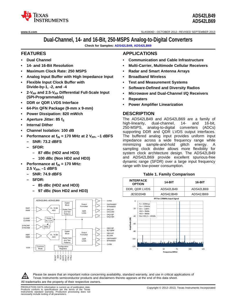
ADS42LB49, ADS42LB69
SYNCINP,
MSYNCIN
OVRA
CT
RL
1
CT
RL
2
DA[3:0]P,
DA[3:0]M
Output
Formatter
QDR
LVDS
DBCLKP,
MBCLK
DBFRAMEP,
MBFRAME
DB[3:0]P,
MB[3:0]M
Output
Formatter
QDR
LVDS
OVRB
Divide
by 1,2,4
Delay
14-, 16-Bit
ADC
Digital
Block
Digital Gain
and Test
Patterns
-120
-100
-80
-60
-40
-20
0
0 25 50 75 100 125
Am
pli
tud
e(d
B)
Frequency (MHz)
FFT for 170MHz Input Signal
Fs = 250Msps
Fin = 170MHz
Ain = -1dBFS
HD2 = 90dBc
HD3 = 89dBc
Non HD2,3 = 100dBc
ADS42LB49ADS42LB69
www.ti.com SLAS904D –OCTOBER 2012–REVISED SEPTEMBER 2013
Dual-Channel, 14- and 16-Bit, 250-MSPS Analog-to-Digital ConvertersCheck for Samples: ADS42LB49, ADS42LB69
1FEATURES APPLICATIONS2• Dual Channel • Communication and Cable Infrastructure• 14- and 16-Bit Resolution • Multi-Carrier, Multimode Cellular Receivers• Maximum Clock Rate: 250 MSPS • Radar and Smart Antenna Arrays• Analog Input Buffer with High Impedance Input • Broadband Wireless• Flexible Input Clock Buffer with • Test and Measurement Systems
Divide-by-1, -2, and -4 • Software-Defined and Diversity Radios• 2-VPP and 2.5-VPP Differential Full-Scale Input • Microwave and Dual-Channel I/Q Receivers
(SPI-Programmable) • Repeaters• DDR or QDR LVDS Interface • Power Amplifier Linearization• 64-Pin QFN Package (9-mm x 9-mm)• Power Dissipation: 820 mW/ch DESCRIPTION
The ADS42LB49 and ADS42LB69 are a family of• Aperture Jitter: 85 fShigh-linearity, dual-channel, 14- and 16-bit,• Internal Dither 250-MSPS, analog-to-digital converters (ADCs)
• Channel Isolation: 100 dB supporting DDR and QDR LVDS output interfaces.The buffered analog input provides uniform input• Performance at fIN = 170 MHz at 2 VPP, –1 dBFSimpedance across a wide frequency range while– SNR: 73.2 dBFSminimizing sample-and-hold glitch energy. A
– SFDR: sampling clock divider allows more flexibility for– 87 dBc (HD2 and HD3) system clock architecture design. The ADS42LB49
and ADS42LB69 provide excellent spurious-free– 100 dBc (Non HD2 and HD3)dynamic range (SFDR) over a large input frequency• Performance at fIN = 170 MHz: range with low-power consumption.
2.5 VPP, –1 dBFS– SNR: 74.9 dBFS Table 1. Family Comparison– SFDR: INTERFACE 14-BIT 16-BITOPTION– 85 dBc (HD2 and HD3)
DDR, QDR LVDS ADS42LB49 ADS42LB69– 97 dBc (Non HD2 and HD3)JESD204B ADS42JB49 ADS42JB69
1
Please be aware that an important notice concerning availability, standard warranty, and use in critical applications ofTexas Instruments semiconductor products and disclaimers thereto appears at the end of this data sheet.
2All trademarks are the property of their respective owners.PRODUCTION DATA information is current as of publication date. Copyright © 2012–2013, Texas Instruments IncorporatedProducts conform to specifications per the terms of the TexasInstruments standard warranty. Production processing does notnecessarily include testing of all parameters.

ADS42LB49ADS42LB69
SLAS904D –OCTOBER 2012–REVISED SEPTEMBER 2013 www.ti.com
This integrated circuit can be damaged by ESD. Texas Instruments recommends that all integrated circuits be handled withappropriate precautions. Failure to observe proper handling and installation procedures can cause damage.
ESD damage can range from subtle performance degradation to complete device failure. Precision integrated circuits may be moresusceptible to damage because very small parametric changes could cause the device not to meet its published specifications.
ORDERING INFORMATION (1)
(1) For the most current package and ordering information, see the Package Option Addendum at the end of this document, or visit thedevice product folder at www.ti.com.
ABSOLUTE MAXIMUM RATINGSOver operating free-air temperature range, unless otherwise noted.
VALUEUNIT
MIN MAXAVDD3V –0.3 3.6 V
Supply voltage range AVDD –0.3 2.1 VDRVDD –0.3 2.1 V
Voltage between AGND and DGND –0.3 0.3 VINA, INBP, INA, INBM –0.3 3 VCLKINP, CLKINM –0.3 AVDD + 0.3 V
Voltage applied to input pinsSYNCINP, SYNCINM –0.3 AVDD + 0.3 VSCLK, SEN, SDATA, RESET, CTRL1, CTRL2 –0.3 3.9 VOperating free-air, TA –40 +85 °C
Temperature range Operating junction, TJ +125 °CStorage, Tstg –65 +150 °C
Electrostatic discharge (ESD) Human body model (HBM) 2 kVratings
THERMAL INFORMATIONADS42LB49,ADS42LB69
THERMAL METRIC (1) UNITSRGC (QFN)64 PINS
θJA Junction-to-ambient thermal resistance 22.9θJCtop Junction-to-case (top) thermal resistance 7.1θJB Junction-to-board thermal resistance 2.5
°C/WψJT Junction-to-top characterization parameter 0.1ψJB Junction-to-board characterization parameter 2.5θJCbot Junction-to-case (bottom) thermal resistance 0.2
(1) For more information about traditional and new thermal metrics, see the IC Package Thermal Metrics application report, SPRA953.
2 Submit Documentation Feedback Copyright © 2012–2013, Texas Instruments Incorporated
Product Folder Links: ADS42LB49 ADS42LB69
ADS42LB49ADS42LB69
www.ti.com SLAS904D –OCTOBER 2012–REVISED SEPTEMBER 2013
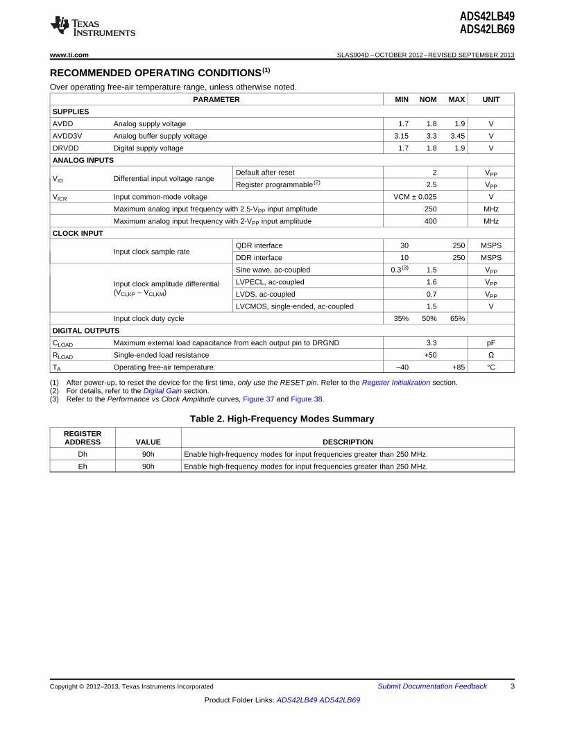
RECOMMENDED OPERATING CONDITIONS (1)
Over operating free-air temperature range, unless otherwise noted.PARAMETER MIN NOM MAX UNIT
SUPPLIESAVDD Analog supply voltage 1.7 1.8 1.9 VAVDD3V Analog buffer supply voltage 3.15 3.3 3.45 VDRVDD Digital supply voltage 1.7 1.8 1.9 VANALOG INPUTS
Default after reset 2 VPPVID Differential input voltage rangeRegister programmable (2) 2.5 VPP
VICR Input common-mode voltage VCM ± 0.025 VMaximum analog input frequency with 2.5-VPP input amplitude 250 MHzMaximum analog input frequency with 2-VPP input amplitude 400 MHz
CLOCK INPUTQDR interface 30 250 MSPS
Input clock sample rateDDR interface 10 250 MSPSSine wave, ac-coupled 0.3 (3) 1.5 VPP
LVPECL, ac-coupled 1.6 VPPInput clock amplitude differential(VCLKP – VCLKM) LVDS, ac-coupled 0.7 VPP
LVCMOS, single-ended, ac-coupled 1.5 VInput clock duty cycle 35% 50% 65%
DIGITAL OUTPUTSCLOAD Maximum external load capacitance from each output pin to DRGND 3.3 pFRLOAD Single-ended load resistance +50 ΩTA Operating free-air temperature –40 +85 °C
(1) After power-up, to reset the device for the first time, only use the RESET pin. Refer to the Register Initialization section.(2) For details, refer to the Digital Gain section.(3) Refer to the Performance vs Clock Amplitude curves, Figure 37 and Figure 38.
Table 2. High-Frequency Modes SummaryREGISTERADDRESS VALUE DESCRIPTION
Dh 90h Enable high-frequency modes for input frequencies greater than 250 MHz.Eh 90h Enable high-frequency modes for input frequencies greater than 250 MHz.
Copyright © 2012–2013, Texas Instruments Incorporated Submit Documentation Feedback 3
Product Folder Links: ADS42LB49 ADS42LB69

ADS42LB49ADS42LB69
SLAS904D –OCTOBER 2012–REVISED SEPTEMBER 2013 www.ti.com
ELECTRICAL CHARACTERISTICS: ADS42LB69 (16-Bit)Typical values are at TA = +25°C, AVDD = 1.8 V, AVDD3V = 3.3 V, DRVDD = 1.8 V, 50% clock duty cycle, –1-dBFSdifferential analog input, and sampling rate = 250 MSPS, unless otherwise noted. Minimum and maximum values are acrossthe full temperature range of TMIN = –40°C to TMAX = +85°C, AVDD = 1.8 V, AVDD3V = 3.3 V, DRVDD = 1.8 V.
2-VPP FULL-SCALE 2.5-VPP FULL-SCALEPARAMETER TEST CONDITIONS UNITS
MIN TYP MAX MIN TYP MAXfIN = 10 MHz 73.9 75.8 dBFSfIN = 70 MHz 73.7 75.5 dBFS
SNR Signal-to-noise ratiofIN = 170 MHz 70.8 73.2 74.7 dBFSfIN = 230 MHz 72.8 74.1 dBFSfIN = 10 MHz 73.7 75.1 dBFSfIN = 70 MHz 73.6 75.3 dBFS
SINAD Signal-to-noise and distortion ratiofIN = 170 MHz 69.6 73.1 74.2 dBFSfIN = 230 MHz 72.5 73.4 dBFSfIN = 10 MHz 87 83 dBc
Spurious-free dynamic range fIN = 70 MHz 90 88 dBcSFDR (including second and third
fIN = 170 MHz 81 87 85 dBcharmonic distortion)fIN = 230 MHz 86 83 dBcfIN = 10 MHz 86 82 dBcfIN = 70 MHz 89 87 dBc
THD Total harmonic distortionfIN = 170 MHz 78 85 82 dBcfIN = 230 MHz 83 81 dBcfIN = 10 MHz 97 95 dBcfIN = 70 MHz 90 88 dBc
HD2 2nd-order harmonic distortionfIN = 170 MHz 81 87 85 dBcfIN = 230 MHz 86 84 dBcfIN = 10 MHz 87 83 dBcfIN = 70 MHz 96 94 dBc
HD3 3rd-order harmonic distortionfIN = 170 MHz 81 91 85 dBcfIN = 230 MHz 87 83 dBcfIN = 10 MHz 102 103 dBc
Worst spur fIN = 70 MHz 101 103 dBc(other than second and third
fIN = 170 MHz 87 101 101 dBcharmonics)fIN = 230 MHz 100 100 dBcf1 = 46 MHz, f2 = 50 MHz, 97 94 dBFSeach tone at –7 dBFSTwo-tone intermodulationIMD distortion f1 = 185 MHz, f2 = 190 MHz, 94 90 dBFSeach tone at –7 dBFS20-MHz, full-scale signal onchannel under observation;Crosstalk 100 100 dB170-MHz, full-scale signal onother channelRecovery to within 1% (of full- ClockInput overload recovery scale) for 6-dB overload with sine- 1 1 cyclewave inputFor 50-mVPP signal on AVDDPSRR AC power-supply rejection ratio > 40 > 40 dBsupply, up to 10 MHz
ENOB Effective number of bits fIN = 170 MHz 11.85 12.03 LSBsDNL Differential nonlinearity fIN = 170 MHz ±0.6 ±0.6 LSBsINL Integrated nonlinearity fIN = 170 MHz ±3 ±8 ±3.5 LSBs
4 Submit Documentation Feedback Copyright © 2012–2013, Texas Instruments Incorporated
Product Folder Links: ADS42LB49 ADS42LB69

ADS42LB49ADS42LB69
www.ti.com SLAS904D –OCTOBER 2012–REVISED SEPTEMBER 2013
ELECTRICAL CHARACTERISTICS: ADS42LB49 (14-Bit)Typical values are at TA = +25°C, AVDD = 1.8 V, AVDD3V = 3.3 V, DRVDD = 1.8 V, 50% clock duty cycle, –1-dBFSdifferential analog input, and sampling rate = 250 MSPS, unless otherwise noted. Minimum and maximum values are acrossthe full temperature range of TMIN = –40°C to TMAX = +85°C, AVDD = 1.8 V, AVDD3V = 3.3 V, DRVDD = 1.8 V.
2-VPP FULL-SCALE 2.5-VPP FULL-SCALEPARAMETER TEST CONDITIONS UNITS
MIN TYP MAX MIN TYP MAXfIN = 10 MHz 73.3 74.9 dBFSfIN = 70 MHz 73.1 74.7 dBFS
SNR Signal-to-noise ratiofIN = 170 MHz 69.5 72.7 74.1 dBFSfIN = 230 MHz 72.3 73.5 dBFSfIN = 10 MHz 73.1 74.1 dBFSfIN = 70 MHz 73.1 74.4 dBFS
SINAD Signal-to-noise and distortion ratiofIN = 170 MHz 68.5 72.6 73.6 dBFSfIN = 230 MHz 72 72.9 dBFSfIN = 10 MHz 87 82 dBc
Spurious-free dynamic range fIN = 70 MHz 90 88 dBcSFDR (including second and third
fIN = 170 MHz 79 87 85 dBcharmonic distortion)fIN = 230 MHz 86 83 dBcfIN = 10 MHz 86 81 dBcfIN = 70 MHz 89 87 dBc
THD Total harmonic distortionfIN = 170 MHz 76 85 82 dBcfIN = 230 MHz 83 81 dBcfIN = 10 MHz 97 95 dBcfIN = 70 MHz 90 88 dBc
HD2 2nd-order harmonic distortionfIN = 170 MHz 79 87 85 dBcfIN = 230 MHz 86 84 dBcfIN = 10 MHz 87 82 dBcfIN = 70 MHz 96 94 dBc
HD3 3rd-order harmonic distortionfIN = 170 MHz 79 91 85 dBcfIN = 230 MHz 87 83 dBcfIN = 10 MHz 104 103 dBc
Worst spur fIN = 70 MHz 101 103 dBc(other than second and third
fIN = 170 MHz 87 100 101 dBcharmonics)fIN = 230 MHz 99 100 dBcf1 = 46 MHz, f2 = 50 MHz, 99 95 dBFSeach tone at –7 dBFSTwo-tone intermodulationIMD distortion f1 = 185 MHz, f2 = 190 MHz, 93 93 dBFSeach tone at –7 dBFS20-MHz, full-scale signal onchannel under observation;Crosstalk 100 90 dB170-MHz, full-scale signal onother channelRecovery to within 1% (of full- ClockInput overload recovery scale) for 6-dB overload with sine- 1 1 cyclewave inputFor a 50-mVPP signal on AVDDPSRR AC power-supply rejection ratio > 40 > 40 dBsupply, up to 10 MHz
ENOB Effective number of bits fIN = 170 MHz 11.76 11.93 LSBsDNL Differential nonlinearity fIN = 170 MHz ±0.15 ±0.15 LSBsINL Integrated nonlinearity fIN = 170 MHz ±0.75 ±3 ±0.9 LSBs
Copyright © 2012–2013, Texas Instruments Incorporated Submit Documentation Feedback 5
Product Folder Links: ADS42LB49 ADS42LB69

ADS42LB49ADS42LB69
SLAS904D –OCTOBER 2012–REVISED SEPTEMBER 2013 www.ti.com
ELECTRICAL CHARACTERISTICS: GeneralTypical values are at +25°C, AVDD = 1.8 V, AVDD3V = 3.3 V, DRVDD = 1.8 V, 50% clock duty cycle, –1-dBFS differentialanalog input, and sampling rate = 250 MSPS, unless otherwise noted. Minimum and maximum values are across the fulltemperature range: TMIN = –40°C to TMAX = +85°C, AVDD = 1.8 V, AVDD3V = 3.3 V, DRVDD = 1.8 V.
PARAMETER TEST CONDITIONS MIN TYP MAX UNIT
ANALOG INPUTS
Default (after reset) 2 VPPDifferential input voltageVID range Register programmed (1) 2.5 VPP
Differential input resistance (at 170 MHz) 1.2 kΩ
Differential input capacitance (at 170 MHz) 4 pF
With 50-Ω source impedance, and 50-ΩAnalog input bandwidth 900 MHztermination
VCM Common-mode output voltage 1.9 V
VCM output current capability 10 mA
DC ACCURACY
Offset error –20 20 mV
Gain error as a result ofEGREF internal reference inaccuracy ±2 %FS
alone
EGCHAN Gain error of channel alone –5 %FS
Temperature coefficient of 0.01 Δ%/°CEGCHAN
POWER SUPPLY
IAVDD Analog supply current 141 182 mA
IAVDD3V Analog buffer supply current 302 340 mA
Digital and Output buffer External 100-Ω differential termination onIDRVDD 219 245 mAsupply current LVDS outputs
Analog power 253 mW
Analog buffer power 996 mW
Power consumption (includes External 100-Ω differential termination ondigital blocks and output 393 mWLVDS outputsbuffers)
Total power 1.64 1.85 W
Global power-down (both 160 mWchannels)
(1) Refer to the Serial Interface section.
6 Submit Documentation Feedback Copyright © 2012–2013, Texas Instruments Incorporated
Product Folder Links: ADS42LB49 ADS42LB69

CLKIN
SYNCIN
tSU_SYNCIN
Sample N
tH_SYNCIN
ADS42LB49ADS42LB69
www.ti.com SLAS904D –OCTOBER 2012–REVISED SEPTEMBER 2013
TIMING REQUIREMENTS: GeneralTypical values are at +25°C, AVDD = 1.8 V, AVDD3V = 3.3 V, DRVDD = 1.8 V, sampling frequency = 250 MSPS, sine waveinput clock, CLOAD = 3.3 pF, and RLOAD = 100 Ω, unless otherwise noted. Minimum and maximum values are across the fulltemperature range: TMIN = –40°C to TMAX = +85°C, AVDD = 1.8 V, AVDD3V = 3.3 V, DRVDD = 1.7 V to 1.9 V.
PARAMETER DESCRIPTION MIN TYP MAX UNITtA Aperture delay 0.5 0.7 1.1 ns
Aperture delay matching Between two channels of the same device ±70 psBetween two devices at the same temperature andVariation of aperture delay ±150 pssupply voltage.
tJ Aperture jitter 85 fS rmsTime to valid data after coming out of STANDBY 50 100 µsmode
Wakeup time Time to valid data after coming out of GLOBALpower-down mode (in this mode, both channels 250 1000 µspower-down)
ClockDefault latency after reset 14 cyclesClockADC latency (1) Normal OVR latency 14 cyclesClockFast OVR latency 9 cycles
Setup time for SYNCIN Referenced to input clocktSU_SYNCIN 400 psrising edgeHold time for SYNCIN Referenced to input clocktH_SYNCIN 100 psrising edge
(1) Overall latency = ADC latency + tPDI.
TIMING DIAGRAM: General
Figure 1. Timing Diagram for SYNCINP and SYNCINM Inputs
Copyright © 2012–2013, Texas Instruments Incorporated Submit Documentation Feedback 7
Product Folder Links: ADS42LB49 ADS42LB69

ADS42LB49ADS42LB69
SLAS904D –OCTOBER 2012–REVISED SEPTEMBER 2013 www.ti.com
TIMING REQUIREMENTS: DDR LVDS Mode (1)
Typical values are at +25°C, AVDD = 1.8 V, AVDD3V = 3.3 V, DRVDD = 1.8 V, sampling frequency = 250 MSPS, sine waveinput clock, CLOAD = 3.3 pF, and RLOAD = 100 Ω, unless otherwise noted. Minimum and maximum values are across the fulltemperature range: TMIN = –40°C to TMAX = +85°C, AVDD = 1.8 V, AVDD3V = 3.3 V, and DRVDD = 1.7 V to 1.9 V.
PARAMETER DESCRIPTION MIN TYP MAX UNITData valid to zero-crossing of differential output clocktSU Data setup time 0.62 0.82 ns(CLKOUTP – CLKOUTM) (2)
Zero-crossing of differential output clocktHO Data hold time 0.54 0.64 ns(CLKOUTP – CLKOUTM) to data becoming invalid (2)
Input clock rising edge cross-over to output clocktPDI Clock propagation delay 8 10.5 13 ns(CLKOUTP – CLKOUTM) rising edge cross-overDuty cycle of differential clockLVDS bit clock duty cycle 52 %(CLKOUTP – CLKOUTM)
tFALL, Data fall time, Rise time measured from –100 mV to +100 mV 0.14 nstRISE Data rise time 10 MSPS ≤ Sampling frequency ≤ 250 MSPStCLKRISE, Output clock rise time, Rise time measured from –100 mV to +100 mV 0.18 nstCLKFALL Output clock fall time 10 MSPS ≤ Sampling frequency ≤ 250 MSPS
(1) Measurements are done with a transmission line of a 100-Ω characteristic impedance between the device and load. Setup and hold timespecifications take into account the effect of jitter on the output data and clock.
(2) Data valid refers to a logic high of +100 mV and a logic low of –100 mV.
Table 3. DDR LVDS Timings at Lower Sampling FrequenciesCLOCK PROPAGATION
SETUP TIME (ns) HOLD TIME (ns) DELAY (ns)tSU tHO tPDISAMPLING
FREQUENCY (MSPS) MIN TYP MAX MIN TYP MAX MIN TYP MAX80 2.40 2.96 2.16 2.82 9 11.9 15120 1.57 1.92 1.40 1.84 8 11.1 14160 1.17 1.40 1.02 1.36 8 10.6 13200 0.82 1.07 0.72 1.02 8 10.5 13230 0.69 0.91 0.61 0.84 8 10.5 13
8 Submit Documentation Feedback Copyright © 2012–2013, Texas Instruments Incorporated
Product Folder Links: ADS42LB49 ADS42LB69

Sample N Sample N+1
D1
D3
D5
D7
D9
D11
D13
D15
D0
D2
D4
D6
D8
D10
D12
D14
D1
D3
D5
D7
D9
D11
D13
D15
D0
D2
D4
D6
D8
D10
D12
D14
CLKINP
Data Latency: 14 Clock Cycles
CLKOUTP
tPD
CLKOUT edges are centered
within the data valid window
Dx[15:0] E O E E O E O E O E O E O
NN-1tSU
tH
CLKINM
CLKOUTM
tA
Sample NINxP
CLKOUTM
CLKOUTP
Dx0P, Dx0M
Dx2P, Dx2M
Dx4P, Dx4M
Dx6P, Dx6M
Dx8P, Dx8M
Dx10P, Dx10M
Dx12P, Dx12M
Dx14P, Dx14M(16-Bit Version Only)
ADS42LB49ADS42LB69
www.ti.com SLAS904D –OCTOBER 2012–REVISED SEPTEMBER 2013
TIMING DIAGRAM: DDR LVDS Mode
Figure 2. DDR LVDS Output Timing Diagram
Copyright © 2012–2013, Texas Instruments Incorporated Submit Documentation Feedback 9
Product Folder Links: ADS42LB49 ADS42LB69
ADS42LB49ADS42LB69
SLAS904D –OCTOBER 2012–REVISED SEPTEMBER 2013 www.ti.com
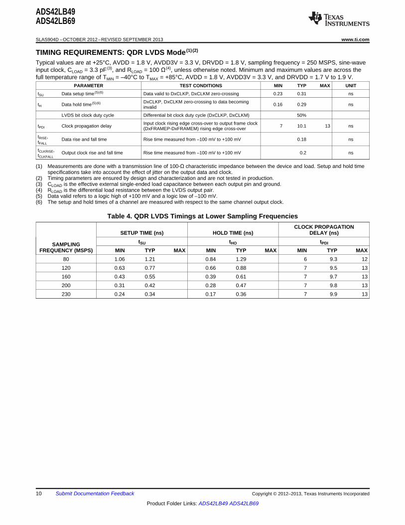
TIMING REQUIREMENTS: QDR LVDS Mode (1) (2)
Typical values are at +25°C, AVDD = 1.8 V, AVDD3V = 3.3 V, DRVDD = 1.8 V, sampling frequency = 250 MSPS, sine-waveinput clock, CLOAD = 3.3 pF (3), and RLOAD = 100 Ω (4), unless otherwise noted. Minimum and maximum values are across thefull temperature range of TMIN = –40°C to TMAX = +85°C, AVDD = 1.8 V, AVDD3V = 3.3 V, and DRVDD = 1.7 V to 1.9 V.
PARAMETER TEST CONDITIONS MIN TYP MAX UNIT
tSU Data setup time (5) (6) Data valid to DxCLKP, DxCLKM zero-crossing 0.23 0.31 ns
DxCLKP, DxCLKM zero-crossing to data becomingtH Data hold time (5) (6) 0.16 0.29 nsinvalid
LVDS bit clock duty cycle Differential bit clock duty cycle (DxCLKP, DxCLKM) 50%
Input clock rising edge cross-over to output frame clocktPDI Clock propagation delay 7 10.1 13 ns(DxFRAMEP-DxFRAMEM) rising edge cross-over
tRISE, Data rise and fall time Rise time measured from –100 mV to +100 mV 0.18 nstFALL
tCLKRISE, Output clock rise and fall time Rise time measured from –100 mV to +100 mV 0.2 nstCLKFALL
(1) Measurements are done with a transmission line of 100-Ω characteristic impedance between the device and load. Setup and hold timespecifications take into account the effect of jitter on the output data and clock.
(2) Timing parameters are ensured by design and characterization and are not tested in production.(3) CLOAD is the effective external single-ended load capacitance between each output pin and ground.(4) RLOAD is the differential load resistance between the LVDS output pair.(5) Data valid refers to a logic high of +100 mV and a logic low of –100 mV.(6) The setup and hold times of a channel are measured with respect to the same channel output clock.
Table 4. QDR LVDS Timings at Lower Sampling FrequenciesCLOCK PROPAGATION
SETUP TIME (ns) HOLD TIME (ns) DELAY (ns)tSU tHO tPDISAMPLING
FREQUENCY (MSPS) MIN TYP MAX MIN TYP MAX MIN TYP MAX80 1.06 1.21 0.84 1.29 6 9.3 12120 0.63 0.77 0.66 0.88 7 9.5 13160 0.43 0.55 0.39 0.61 7 9.7 13200 0.31 0.42 0.28 0.47 7 9.8 13230 0.24 0.34 0.17 0.36 7 9.9 13
10 Submit Documentation Feedback Copyright © 2012–2013, Texas Instruments Incorporated
Product Folder Links: ADS42LB49 ADS42LB69

NN-1
DA0M, DB0M
DA0P, DB0P
15 11 7 3
14 10 6 2
13 9 5 1
12 8 4 0
15 11 7 3
14 10 6 2
13 9 5 1
12 8 4 0
CLKINM
Data Latency: 14 Clock Cycles
Sample N
DxCLKP
N+1
15
14
13
12
TPD
DxCLK edges are centeredin the data valid window.
DA1M, DB1M
DA1P, DB1P
DA2M, DB2M
DA2P, DB2P
DA3M, DB3M
DA3P, DB3P
tsu th
DxFRAMEP
CLKIN, DxCLK, DxFRAMEP (x = A or B) are differential:
KvoÇZZW[]]À]PvoZÁv(o]Ç.
CLKINP
DxCLKM
DxFRAMEM
INxP
tA
ADS42LB49ADS42LB69
www.ti.com SLAS904D –OCTOBER 2012–REVISED SEPTEMBER 2013
TIMING DIAGRAM: QDR LVDS Mode
Figure 3. QDR LVDS Output Timing Diagram
Copyright © 2012–2013, Texas Instruments Incorporated Submit Documentation Feedback 11
Product Folder Links: ADS42LB49 ADS42LB69

DAn_PDBn_P
DAn_MDBn_M
GND
Logic 0
V(1)
ODL = 350 mV-
Logic 1
V(1)
ODH = +350 mV
VOCM
ADS42LB49ADS42LB69
SLAS904D –OCTOBER 2012–REVISED SEPTEMBER 2013 www.ti.com
DIGITAL CHARACTERISTICSThe dc specifications refer to the condition where the digital outputs are not switching, but are permanently at a valid logiclevel '0' or '1'. AVDD = 1.8 V, AVDD3V = 3.3 V, DRVDD = 1.8 V, and, unless otherwise noted.
PARAMETER TEST CONDITIONS MIN TYP MAX UNIT
DIGITAL INPUTS (RESET, SCLK, SDATA, SEN, CTRL1, CTRL2) (1)
VIH High-level input voltage All digital inputs support 1.3 V1.8-V and 3.3-V CMOS
VIL Low-level input voltage 0.4 Vlogic levels
RESET, SDATA, SCLK, VHIGH = 1.8 V 10 µACTRL1, CTRL2 (2)IIH High-level input current
SEN (3) VHIGH = 1.8 V 0 µA
RESET, SDATA, SCLK, VLOW = 0 V 0 µACTRL1, CTRL2IIL Low-level input currentSEN VLOW = 0 V 10 µA
DIGITAL OUTPUTS, CMOS INTERFACE (OVRA, OVRB, SDOUT)
VOH High-level output voltage DRVDD – 0.1 DRVDD V
VOL Low-level output voltage 0 0.1 V
DIGITAL OUTPUTS, LVDS INTERFACE
With an externalVODH High-level output differential voltage 250 350 500 mV100-Ω termination
With an externalVODL Low-level output differential voltage –500 –350 –250 mV100-Ω termination
VOCM Output common-mode voltage 1.05 V
(1) SCLK, SDATA, and SEN function as digital input pins in serial configuration mode.(2) SDATA and SCLK have an internal 150-kΩ pull-down resistor.(3) SEN has an internal 150-kΩ pull-up resistor to AVDD. Because the pull-up resistor is weak, SEN can also be driven by 1.8-V or 3.3-V
CMOS buffers.
(1) With an external 100-Ω termination.
Figure 4. DDR LVDS Output Voltage Levels
12 Submit Documentation Feedback Copyright © 2012–2013, Texas Instruments Incorporated
Product Folder Links: ADS42LB49 ADS42LB69

1
2
3
4
5
6
7
8
9
10
11
12
13
14
15
16
17 18 19 20 21 22 23 24 25 26 27 28 29 30 31 32
48
47
46
45
44
43
42
41
40
39
38
37
36
35
34
33
64 63 62 61 60 59 58 57 56 55 54 53 52 51 50 49
DB8M
DB8P
DB6M
DB6P
DB4M
DB4P
DB2M
DB2P
DB0M
DB0P
DRVDD
CTRL2
AVDD
INBP
INBM
AVDD AVDD
DA8P
DA8M
DA6P
DA6M
DA4P
DA4M
DA2P
DA2M
DA0P
DA0M
AVDD
CTRL1
AVDD
INAP
INAM
AV
DD
3V
SC
LK
SD
ATA
SE
N
SD
OU
T
RE
SE
T
AV
DD
CL
KIN
M
CL
KIN
P
AV
DD
VC
M
RE
SE
RV
ED
SY
NC
INP
SY
NC
INM
AV
DD
AV
DD
3V
GND Pad (Backside)
DR
VD
D
DB
10
P
DB
10
M
DB
12
P
DB
12
M
DB
14
P
DB
14
M
CL
KO
UT
P
CL
KO
UT
M
DA
14
P
DA
14
M
DA
12
P
DA
12
M
DA
10
P
DA
10
M
DR
VD
D
ADS42LB49ADS42LB69
www.ti.com SLAS904D –OCTOBER 2012–REVISED SEPTEMBER 2013
PIN CONFIGURATIONS
RGC PACKAGEQFN-64
(Top View)
Figure 5. ADS42LB69 DDR LVDS
Copyright © 2012–2013, Texas Instruments Incorporated Submit Documentation Feedback 13
Product Folder Links: ADS42LB49 ADS42LB69

ADS42LB49ADS42LB69
SLAS904D –OCTOBER 2012–REVISED SEPTEMBER 2013 www.ti.com
PIN ASSIGNMENTS: ADS42LB69 DDR LVDS OUTPUT INTERFACEPIN
I/O DESCRIPTIONNAME NUMBERINPUT AND REFERENCEINAP, INAM 36, 35 I Differential analog input for channel AINBP, INBM 14, 15 I Differential analog input for channel BVCM 27 O Common-mode voltage for analog inputs, 1.9 VCLOCK AND SYNCCLKINP, CLKINM 25, 24 I Differential clock input for ADCSYNCINP, SYNCINM 29, 30 I External sync input. If not used, connect SYNCINP to GND and SYNCINM to AVDD.CONTROL AND SERIAL
Can be configured as power-down input pin or as OVR output pin for channel A,CTRL1 37 I/O depending on the register bit PDN/OVR FOR CTRL PINS.Can be configured as power-down input pin or as OVR output pin for channel B,CTRL2 12 I/O depending on the register bit PDN/OVR FOR CTRL PINS
Reserved 28 — Do not connectRESET 22 I Hardware reset. Active high.SCLK 18 I Serial interface clock inputSDATA 19 I Serial interface data input.SDOUT 21 O Serial interface data outputSEN 20 I Serial interface enableDATA INTERFACECLKOUTP, 57, 56 O Differential LVDS output clockCLKOUTMDA[14:0]P, DA[14:0]M 39-48, 50-55 O DDR LVDS output interface for channel ADB[14:0]P, DB[14:0]M 1-10, 58-63 O DDR LVDS output interface for channel BPOWER SUPPLY
13, 16, 23, 26, 31,AVDD I Analog 1.8-V power supply33, 36, 38AVDD3V 17, 32 I Analog 3.3 V power supply for analog bufferDRVDD 11, 49, 64 I Digital 1.8-V power supplyGND Ground pad I Ground
14 Submit Documentation Feedback Copyright © 2012–2013, Texas Instruments Incorporated
Product Folder Links: ADS42LB49 ADS42LB69

1
2
3
4
5
6
7
8
9
10
11
12
13
14
15
16
17 18 19 20 21 22 23 24 25 26 27 28 29 30 31 32
48
47
46
45
44
43
42
41
40
39
38
37
36
35
34
33
64 63 62 61 60 59 58 57 56 55 54 53 52 51 50 49
DB6M
DB6P
DB4M
DB4P
DB2M
DB2P
DB0M
DB0P
NC/OVR
NC/OVR
DRVDD
CTRL2
AVDD
INBP
INBM
AVDD AVDD
DA6P
DA6M
DA4P
DA4M
DA2P
DA2M
DA0P
DA0M
NC/OVR
NC/OVR
AVDD
CTRL1
AVDD
INAP
INAM
AV
DD
3V
SC
LK
SD
ATA
SE
N
SD
OU
T
RE
SE
T
AV
DD
CLK
INM
CLK
INP
AV
DD
VC
M
RE
SE
RV
ED
SY
NC
INP
SY
NC
INM
AV
DD
AV
DD
3V
GND Pad (Backside)
DR
VD
D
DR
VD
D
DB
8P
DB
8M
DB
10P
DB
10M
DB
12P
DB
12M
CLK
OU
TP
CLK
OU
TM
DA
12P
DA
12M
DA
10P
DA
10M
DA
8P
DA
8M
ADS42LB49ADS42LB69
www.ti.com SLAS904D –OCTOBER 2012–REVISED SEPTEMBER 2013
RGC PACKAGEQFN-64
(Top View)
Figure 6. ADS42LB49 DDR LVDS
Copyright © 2012–2013, Texas Instruments Incorporated Submit Documentation Feedback 15
Product Folder Links: ADS42LB49 ADS42LB69

ADS42LB49ADS42LB69
SLAS904D –OCTOBER 2012–REVISED SEPTEMBER 2013 www.ti.com
PIN ASSIGNMENTS: ADS42LB49 DDR LVDS OUTPUT INTERFACEPIN
I/O DESCRIPTIONNAME NUMBERINPUT AND REFERENCEINAP, INAM 35, 35 I Differential analog input for channel AINBP, INBM 14, 15 I Differential analog input for channel BVCM 27 O Common-mode voltage for analog inputs, 1.9 VCLOCK AND SYNCCLKINP, CLKINM 25, 24 I Differential clock input for ADCSYNCINP, SYNCINM 29, 30 I External sync input. If not used, connect SYNCINP to GND and SYNCINM to AVDD.CONTROL AND SERIAL
Can be configured as power-down input pin or as OVR output pin for channel A,CTRL1 37 I/O depending on the register bit PDN/OVR FOR CTRL PINS.Can be configured as power-down input pin or as OVR output pin for channel B,CTRL2 12 I/O depending on the register bit PDN/OVR FOR CTRL PINSIf the OVR ON LSB bit is set, these pins can be used because they carry overrangeNC/OVR 9, 10, 39, 40 — information. Otherwise, do not connect these pins.
Reserved 28 — Do not connectRESET 22 I Hardware reset. Active high.SCLK 18 I Serial interface clock inputSDATA 19 I Serial interface data input.SDOUT 21 O Serial interface data outputSEN 20 I Serial interface enableDATA INTERFACECLKOUTP, 57, 56 O Differential LVDS output clockCLKOUTMDA[14:0]P, DA[14:0]M 41-48, 50-55 O DDR LVDS output interface for channel ADB[14:0]P, DB[14:0]M 1-8, 58-63 O DDR LVDS output interface for channel BPOWER SUPPLY
13, 16, 23, 26, 31,AVDD I Analog 1.8-V power supply33, 36, 38AVDD3V 17, 32 I Analog 3.3-V analog supply for analog bufferDRVDD 11, 49, 64 I Digital 1.8-V power supplyGND Ground pad I Ground
16 Submit Documentation Feedback Copyright © 2012–2013, Texas Instruments Incorporated
Product Folder Links: ADS42LB49 ADS42LB69

1
2
3
4
5
6
7
8
9
10
11
12
13
14
15
16
17 18 19 20 21 22 23 24 25 26 27 28 29 30 31 32
48
47
46
45
44
43
42
41
40
39
38
37
36
35
34
33
64 63 62 61 60 59 58 57 56 55 54 53 52 51 50 49
DB1M
DB1P
DBCLKM
DBCLKP
DB2M
DB2P
DB3M
DB3P
DBFRAMEM
DBFRAMEP
DRVDD
CTRL2
AVDD
INBP
INBM
AVDD AVDD
DA2P
DA2M
DACLKP
DACLKM
DA1P
DA1M
DA0P
DA0M
NC
NC
AVDD
CTRL1
AVDD
INAP
INAM
AV
DD
3V
SC
LK
SD
ATA
SE
N
SD
OU
T
RE
SE
T
AV
DD
CL
KIN
M
CL
KIN
P
AV
DD
VC
M
RE
SE
RV
ED
SY
NC
INP
SY
NC
INM
AV
DD
AV
DD
3V
GND Pad (Backside)
DR
VD
D
DR
VD
D
DB
0P
DB
0M
NC
NC
OV
RB
NC
NC
NC
NC
OV
RA
DA
FR
AM
EP
DA
FR
AM
EM
DA
3P
DA
3M
ADS42LB49ADS42LB69
www.ti.com SLAS904D –OCTOBER 2012–REVISED SEPTEMBER 2013
RGC PACKAGEQFN-64
(Top View)
Figure 7. ADS42LB69, ADS42LB49 QDR LVDS
Copyright © 2012–2013, Texas Instruments Incorporated Submit Documentation Feedback 17
Product Folder Links: ADS42LB49 ADS42LB69

ADS42LB49ADS42LB69
SLAS904D –OCTOBER 2012–REVISED SEPTEMBER 2013 www.ti.com
PIN ASSIGNMENTS: QDR LVDS OUTPUT INTERFACEPIN
I/O DESCRIPTIONNAME NUMBERINPUT AND REFERENCEINAP, INAM 34, 35 I Differential analog input for channel AINBP, INBM 14, 15 I Differential analog input for channel BVCM 27 O Common-mode voltage for analog inputs, 1.9 VCLOCK AND SYNCCLKINP, CLKINM 24, 25 I Differential clock input for ADCSYNCINP, SYNCINM 29, 30 I External sync input If not used, connect SYNCINP to GND and SYNCINM to AVDD.CONTROL AND SERIAL
Can be configured as power-down input pin or as OVR output pin for channel A,CTRL1 37 I depending on the register bit PDN/OVR FOR CTRL PINS.Can be configured as power-down input pin or as OVR output pin for channel B,CTRL2 12 I depending on the register bit PDN/OVR FOR CTRL PINS
39, 40, 55-58, 60,NC — Do not connect61Reserved 28 — Do not connectRESET 22 I Hardware reset. Active high.SCLK 18 I Serial interface clock inputSDATA 19 I Serial interface data input.SDOUT 21 O Serial interface data outputSEN 20 I Serial interface enableDATA INTERFACE
41-44, 47, 48, 50,DA[3:0]P, DA[3:0]M O 4-bit QDR LVDS output interface for channel A51DACLKP, DACLKM 45, 46 O Differential output clock for channel ADAFRAMEP, 52, 53 — Differential frame clock output for channel ADAFRAMEMDB[3:0]P, DB[3:0]M 1, 2, 5-8, 62, 63 — 4-bit QDR LVDS output interface for channel BDBCLKP, DBCLKM 3, 4 — Differential output clock for channel ADBFRAMEP, 9, 10 — Differential frame clock output for channel ADBFRAMEMOVRA 54 O Overrange indication channel AOVRB 59 O Overrange indication channel APOWER SUPPLY
13, 16, 23, 26, 31,AVDD I Analog 1.8-V power supply33, 36, 38AVDD3V 17, 32 I Analog 3.3-V power supply for analog bufferDRVDD 11, 49, 64 I Digital 1.8-V power supplyGND Ground pad I Ground
18 Submit Documentation Feedback Copyright © 2012–2013, Texas Instruments Incorporated
Product Folder Links: ADS42LB49 ADS42LB69

CLKINP,
MCLKIN
INAP,
I MNA
Configuration
Registers
SC
LK
SE
N
SD
ATA
SD
OU
T
RE
SE
T
Common
ModeVCM
INBP,
MINB
14-Bit
ADC
Digital
Block
Digital Gain
and Test
Patterns
ADS42LB49
SYNCINP,
MSYNCIN
CT
RL
1
CT
RL
2
DA[13:0]P,
DA[13:0]M
CLKOUTP,
CLKOUTM
Output
Formatter
DDR LVDS
DB[13:0]P,
DB[13:0]M
Output
Formatter
DDR LVDS
Divide
by 1,2,4
Delay
Digital
Block
Digital Gain
and Test
Patterns
14-Bit
ADC
CLKINP,
CLKINM
INAP,
INAM
Configuration
RegistersS
CLK
SE
N
SD
ATA
SD
OU
T
RE
SE
TCommon
ModeVCM
INBP,
INBM
16-Bit
ADC
Digital
Block
Digital Gain
and Test
Patterns
ADS42LB69
SYNCINP,
SYNCINM
CT
RL
1
CT
RL
2
DA[15:0]P,
DA[15:0]M
CLKOUTP,
CLKOUTM
Output
Formatter
DDR LVDS
DB[15:0]P,
DB[15:0]M
Output
Formatter
DDR LVDS
Divide
by 1,2,4
Delay
Digital
Block
Digital Gain
and Test
Patterns
16-Bit
ADC
ADS42LB49ADS42LB69
www.ti.com SLAS904D –OCTOBER 2012–REVISED SEPTEMBER 2013
FUNCTIONAL BLOCK DIAGRAMS
Figure 8. ADS42LB69 DDR LVDS
Figure 9. ADS42LB49 DDR LVDS
Copyright © 2012–2013, Texas Instruments Incorporated Submit Documentation Feedback 19
Product Folder Links: ADS42LB49 ADS42LB69

CLKINP,
CLKINM
INAP,
INAM
Configuration
Registers
SC
LK
SE
N
SD
ATA
SD
OU
T
RE
SE
T
Common
ModeVCM
DACLKP,
D MACLK
DAFRAMEP,
MAFRAME
INBP,
MINB
14-, 16-Bit
ADC
Digital
Block
Digital Gain
and Test
Patterns
ADS42LB49, ADS42LB69
SYNCINP,
MSYNCIN
OVRA
CT
RL
1
CT
RL
2
DA[3:0]P,
DA[3:0]M
Output
Formatter
QDR
LVDS
DBCLKP,
MBCLK
DBFRAMEP,
MBFRAME
DB[3:0]P,
MB[3:0]M
Output
Formatter
QDR
LVDS
OVRB
Divide
by 1,2,4
Delay
14-, 16-Bit
ADC
Digital
Block
Digital Gain
and Test
Patterns
ADS42LB49ADS42LB69
SLAS904D –OCTOBER 2012–REVISED SEPTEMBER 2013 www.ti.com
Figure 10. ADS42LB69, ADS42LB49 QDR LVDS
20 Submit Documentation Feedback Copyright © 2012–2013, Texas Instruments Incorporated
Product Folder Links: ADS42LB49 ADS42LB69

−120
−100
−80
−60
−40
−20
0
0 25 50 75 100 125
Frequency (MHz)
Am
plitu
de (
dBF
S)
FIN = 300 MHzSFDR = 76 dBcSNR = 72.2 dBFSSINAD = 70.5 dBFSTHD = 74 dBcSFDR Non HD2,HD3= 97 dBc
G003
−120
−100
−80
−60
−40
−20
0
0 25 50 75 100 125
Frequency (MHz)
Am
plitu
de (
dBF
S)
FIN = 10 MHzSFDR = 84 dBcSNR = 75.7 dBFSSINAD = 75.2 dBFSTHD = 83 dBcSFDR Non HD2, HD3 = 104 dBc
G004
−120
−100
−80
−60
−40
−20
0
0 25 50 75 100 125
Frequency (MHz)
Am
plitu
de (
dBF
S)
FIN = 10 MHzSFDR = 88 dBcSNR = 74 dBFSSINAD = 73.9 dBFSTHD = 87 dBcSFDR Non HD2, HD3 = 102 dBc
G001
−120
−100
−80
−60
−40
−20
0
0 25 50 75 100 125
Frequency (MHz)
Am
plitu
de (
dBF
S)
FIN = 170 MHzSFDR = 90 dBcSNR = 73.1 dBFSSINAD = 73 dBFSTHD = 87 dBcSFDR Non HD2, HD3 = 100 dBc
G002
ADS42LB49ADS42LB69
www.ti.com SLAS904D –OCTOBER 2012–REVISED SEPTEMBER 2013
TYPICAL CHARACTERISTICS: ADS42LB69Typical values are at TA = +25°C, full temperature range is TMIN = –40°C to TMAX = +85°C, ADC sampling rate = 250 MSPS,50% clock duty cycle, QDR interface, AVDD3V = 3.3 V, AVDD = DRVDD = 1.8 V, –1-dBFS differential input, and 32k-point
FFT, unless otherwise noted.
Figure 11. FFT FOR 10-MHz INPUT SIGNAL Figure 12. FFT FOR 170-MHz INPUT SIGNAL
Figure 13. FFT FOR 300-MHz INPUT SIGNAL Figure 14. FFT FOR 10-MHz INPUT SIGNAL(2.5-VPP Full-Scale)
Copyright © 2012–2013, Texas Instruments Incorporated Submit Documentation Feedback 21
Product Folder Links: ADS42LB49 ADS42LB69

−120
−100
−80
−60
−40
−20
0
0 25 50 75 100 125
Frequency (MHz)
Am
plitu
de (
dBF
S)
Each Tone at−7 dBFS AmplitudefIN1 = 46 MHzfIN2 = 50 MHz2−Tone IMD = 97 dBFSSFDR = 101 dBFS
G007
−120
−100
−80
−60
−40
−20
0
0 25 50 75 100 125
Frequency (MHz)
Am
plitu
de (
dBF
S)
Each Tone at−36 dBFS AmplitudefIN1 = 46 MHzfIN2 = 50 MHz2−Tone IMD = 101 dBFSSFDR = 103 dBFS
G008
−120
−100
−80
−60
−40
−20
0
0 25 50 75 100 125
Frequency (MHz)
Am
plitu
de (
dBF
S)
FIN = 170 MHzSFDR = 87 dBcSNR = 74.7 dBFSSINAD = 74.3 dBFSTHD = 84 dBcSFDR Non HD2, HD3 = 93 dBc
G005
−120
−100
−80
−60
−40
−20
0
0 25 50 75 100 125
Frequency (MHz)
Am
plitu
de (
dBF
S)
FIN = 300 MHzSFDR = 72 dBcSNR = 73.3 dBFSSINAD = 70 dBFSTHD = 70 dBcSFDR Non HD2, HD3 = 93 dBc
G006
ADS42LB49ADS42LB69
SLAS904D –OCTOBER 2012–REVISED SEPTEMBER 2013 www.ti.com
TYPICAL CHARACTERISTICS: ADS42LB69 (continued)Typical values are at TA = +25°C, full temperature range is TMIN = –40°C to TMAX = +85°C, ADC sampling rate = 250 MSPS,50% clock duty cycle, QDR interface, AVDD3V = 3.3 V, AVDD = DRVDD = 1.8 V, –1-dBFS differential input, and 32k-pointFFT, unless otherwise noted.
Figure 15. FFT FOR 170-MHz INPUT SIGNAL Figure 16. FFT FOR 300-MHz INPUT SIGNAL(2.5-VPP Full-Scale) (2.5-VPP Full-Scale)
Figure 17. FFT FOR TWO-TONE INPUT SIGNAL Figure 18. FFT FOR TWO-TONE INPUT SIGNAL(At –7 dBFS, 46 MHz and 50 MHz) (At –36 dBFS, 46 MHz and 50 MHz)
22 Submit Documentation Feedback Copyright © 2012–2013, Texas Instruments Incorporated
Product Folder Links: ADS42LB49 ADS42LB69

−108
−106
−104
−102
−100
−98
−96
−94
−36 −33 −30 −27 −24 −21 −18 −15 −12 −9 −7
Each Tone Amplitude (dBFS)
Tw
o −
Ton
e IM
D (
dBF
S)
fIN1 = 46 MHzfIN2 = 50 MHz
G011
−108
−106
−104
−102
−100
−98
−96
−94
−92
−36 −33 −30 −27 −24 −21 −18 −15 −12 −9 −7
Each Tone Amplitude (dBFS)
Tw
o −
Ton
e IM
D (
dBF
S)
fIN1 = 185 MHzfIN2 = 190 MHz
G012
−120
−100
−80
−60
−40
−20
0
0 25 50 75 100 125
Frequency (MHz)
Am
plitu
de (
dBF
S)
Each Tone at−7 dBFS AmplitudefIN1 = 185 MHzfIN2 = 190 MHz2−Tone IMD = 94 dBFSSFDR = 96 dBFS
G008
−120
−100
−80
−60
−40
−20
0
0 25 50 75 100 125
Frequency (MHz)
Am
plitu
de (
dBF
S)
Each Tone at−36 dBFS AmplitudefIN1 = 185 MHzfIN2 = 190 MHz2−Tone IMD = 107 dBFSSFDR = 108 dBFS
G010
ADS42LB49ADS42LB69
www.ti.com SLAS904D –OCTOBER 2012–REVISED SEPTEMBER 2013
TYPICAL CHARACTERISTICS: ADS42LB69 (continued)Typical values are at TA = +25°C, full temperature range is TMIN = –40°C to TMAX = +85°C, ADC sampling rate = 250 MSPS,50% clock duty cycle, QDR interface, AVDD3V = 3.3 V, AVDD = DRVDD = 1.8 V, –1-dBFS differential input, and 32k-pointFFT, unless otherwise noted.
Figure 19. FFT FOR TWO-TONE INPUT SIGNAL Figure 20. FFT FOR TWO-TONE INPUT SIGNAL(At –7 dBFS, 185 MHz and 190 MHz) (At –36 dBFS, 185 MHz and 190 MHz)
Figure 21. IMD3 vs INPUT AMPLITUDE Figure 22. IMD3 vs INPUT AMPLITUDE(46 MHz and 50 MHz) (185 MHz and 190 MHz)
Copyright © 2012–2013, Texas Instruments Incorporated Submit Documentation Feedback 23
Product Folder Links: ADS42LB49 ADS42LB69

60
65
70
75
80
85
90
95
100
105
110
−2−1.5−1−0.5 0 0.5 1 1.5 2 2.5 3 3.5 4 4.5 5 5.5 6
Digital Gain (dB)
SF
DR
(dB
c)
10 MHz70 MHz100 MHz130 MHz
170 MHz230 MHz270 MHz350 MHz
400 MHz491 MHz
G015
66
68
70
72
74
76
78
−2−1.5−1−0.5 0 0.5 1 1.5 2 2.5 3 3.5 4 4.5 5 5.5 6
Gain (dB)
SN
R (
dBF
S)
10 MHz70 MHz100 MHz130 MHz
170 MHz230 MHz270 MHz350 MHz
400 MHz491 Mhz
G016
55
60
65
70
75
80
85
90
95
100
0 50 100 150 200 250 300 350 400
Input Frequency (MHz)
SF
DR
(dB
c)
2−VPP Full−Scale2.5−VPP Full−Scale
G013
70
71
72
73
74
75
76
77
0 50 100 150 200 250 300 350 400
Input Frequency (MHz)
SN
R (
dBF
S)
2−VPP Full−Scale2.5−VPP Full−Scale
G014
ADS42LB49ADS42LB69
SLAS904D –OCTOBER 2012–REVISED SEPTEMBER 2013 www.ti.com
TYPICAL CHARACTERISTICS: ADS42LB69 (continued)Typical values are at TA = +25°C, full temperature range is TMIN = –40°C to TMAX = +85°C, ADC sampling rate = 250 MSPS,50% clock duty cycle, QDR interface, AVDD3V = 3.3 V, AVDD = DRVDD = 1.8 V, –1-dBFS differential input, and 32k-pointFFT, unless otherwise noted.
Figure 23. SFDR vs INPUT FREQUENCY Figure 24. SNR vs INPUT FREQUENCY
Figure 25. SFDR vs DIGITAL GAIN Figure 26. SNR vs DIGITAL GAIN
24 Submit Documentation Feedback Copyright © 2012–2013, Texas Instruments Incorporated
Product Folder Links: ADS42LB49 ADS42LB69

1.85 1.87 1.9 1.93 1.9582
84
86
88
90
92
94
96
72.5
73
73.5
74
74.5
75
75.5
76
Input Common−Mode Voltage (V)
SF
DR
(dB
c)
SN
R (
dBF
S)
SFDRSNR
Input Frequency = 70 MHz
G019
1.85 1.87 1.9 1.93 1.9580
83
86
89
92
95
98
72.5
73
73.5
74
74.5
75
75.5
Input Common−Mode Voltage (V)
SF
DR
(dB
c)
SN
R (
dBF
S)
SFDRSNR
Input Frequency = 170 MHz
G020
−70 −60 −50 −40 −30 −20 −10 071.5
72
72.5
73
73.5
74
74.5
75
75.5
76
76.5
77
20
30
40
50
60
70
80
90
100
110
120
130
Amplitude (dBFS)
SN
R (
dBF
S)
SF
DR
(dB
c,dB
FS
)
SNR(dBFS)SFDR(dBc)SFDR(dBFS)
Input Frequency = 70 MHz
G017
−70 −60 −50 −40 −30 −20 −10 072
72.5
73
73.5
74
74.5
75
75.5
76
76.5
77
77.5
20
30
40
50
60
70
80
90
100
110
120
130
Amplitude (dBFS)S
NR
(dB
FS
)
SF
DR
(dB
c,dB
FS
)
SNR(dBFS)SFDR(dBc)SFDR(dBFS)
Input Frequency = 170 MHz
G018
ADS42LB49ADS42LB69
www.ti.com SLAS904D –OCTOBER 2012–REVISED SEPTEMBER 2013
TYPICAL CHARACTERISTICS: ADS42LB69 (continued)Typical values are at TA = +25°C, full temperature range is TMIN = –40°C to TMAX = +85°C, ADC sampling rate = 250 MSPS,50% clock duty cycle, QDR interface, AVDD3V = 3.3 V, AVDD = DRVDD = 1.8 V, –1-dBFS differential input, and 32k-pointFFT, unless otherwise noted.
Figure 27. PERFORMANCE ACROSS INPUT AMPLITUDE Figure 28. PERFORMANCE ACROSS INPUT AMPLITUDE(170 MHz)(70 MHz)
Figure 29. PERFORMANCE vs INPUT COMMON-MODE Figure 30. PERFORMANCE vs INPUT COMMON-MODEVOLTAGE (70 MHz) VOLTAGE (170 MHz)
Copyright © 2012–2013, Texas Instruments Incorporated Submit Documentation Feedback 25
Product Folder Links: ADS42LB49 ADS42LB69

78
81
84
87
90
93
96
99
−40 −15 10 35 60 85Temperature (°C)
SF
DR
(dB
c)
AVDD3V = 3.15 VAVDD3V = 3.2 VAVDD3V = 3.25 VAVDD3V = 3.3 V
AVDD3V = 3.35 VAVDD3V = 3.4 VAVDD3V = 3.45 V
Input Frequency = 170 MHz
G023
72
72.5
73
73.5
74
74.5
75
−40 −15 10 35 60 85Temperature (°C)
SN
R (
dBF
S)
AVDD3V = 3.15 VAVDD3V = 3.2 VAVDD3V = 3.25 VAVDD3V = 3.3 V
AVDD3V = 3.35 VAVDD3V = 3.4 VAVDD3V = 3.45 V
Input Frequency = 170 MHz
G024
78
81
84
87
90
93
96
99
−40 −15 10 35 60 85Temperature (°C)
SF
DR
(dB
c)
AVDD = 1.7 VAVDD = 1.75 VAVDD = 1.8 V
AVDD = 1.85 VAVDD = 1.9 V
Input Frequency = 170 MHz
G021
72
72.5
73
73.5
74
74.5
75
−40 −15 10 35 60 85Temperature (°C)
SN
R (
dBF
S)
AVDD = 1.7 VAVDD = 1.75VAVDD = 1.8 V
AVDD = 1.85 VAVDD = 1.9 V
Input Frequency = 170 MHz
G022
ADS42LB49ADS42LB69
SLAS904D –OCTOBER 2012–REVISED SEPTEMBER 2013 www.ti.com
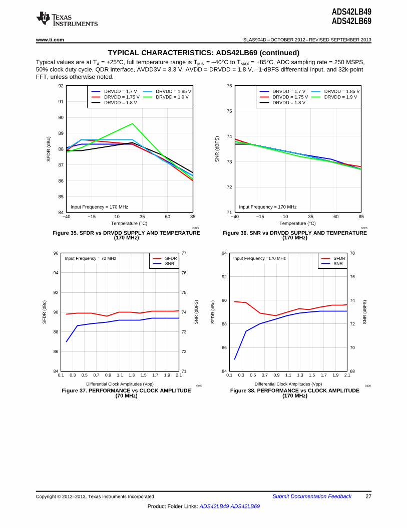
TYPICAL CHARACTERISTICS: ADS42LB69 (continued)Typical values are at TA = +25°C, full temperature range is TMIN = –40°C to TMAX = +85°C, ADC sampling rate = 250 MSPS,50% clock duty cycle, QDR interface, AVDD3V = 3.3 V, AVDD = DRVDD = 1.8 V, –1-dBFS differential input, and 32k-pointFFT, unless otherwise noted.
Figure 31. SFDR vs AVDD SUPPLY AND TEMPERATURE Figure 32. SNR vs AVDD SUPPLY AND TEMPERATURE(170 MHz) (170 MHz)
Figure 33. SFDR vs AVDD_BUF SUPPLY AND Figure 34. SNR vs AVDD_BUF SUPPLY ANDTEMPERATURE (170 MHz) TEMPERATURE (170 MHz)
26 Submit Documentation Feedback Copyright © 2012–2013, Texas Instruments Incorporated
Product Folder Links: ADS42LB49 ADS42LB69
0.1 0.3 0.5 0.7 0.9 1.1 1.3 1.5 1.7 1.9 2.184
86
88
90
92
94
96
71
72
73
74
75
76
77
Differential Clock Amplitudes (Vpp)
SF
DR
(dB
c)
SN
R (
dBF
S)
SFDRSNR
Input Frequency = 70 MHz
G027
0.1 0.3 0.5 0.7 0.9 1.1 1.3 1.5 1.7 1.9 2.184
86
88
90
92
94
68
70
72
74
76
78
Differential Clock Amplitudes (Vpp)
SF
DR
(dB
c)
SN
R (
dBF
S)
SFDRSNR
Input Frequency =170 MHz
G028
84
85
86
87
88
89
90
91
92
−40 −15 10 35 60 85Temperature (°C)
SF
DR
(dB
c)
DRVDD = 1.7 VDRVDD = 1.75 VDRVDD = 1.8 V
DRVDD = 1.85 VDRVDD = 1.9 V
Input Frequency = 170 MHz
G025
71
72
73
74
75
76
−40 −15 10 35 60 85Temperature (°C)
SN
R (
dBF
S)
DRVDD = 1.7 VDRVDD = 1.75 VDRVDD = 1.8 V
DRVDD = 1.85 VDRVDD = 1.9 V
Input Frequency = 170 MHz
G026
ADS42LB49ADS42LB69
www.ti.com SLAS904D –OCTOBER 2012–REVISED SEPTEMBER 2013
TYPICAL CHARACTERISTICS: ADS42LB69 (continued)Typical values are at TA = +25°C, full temperature range is TMIN = –40°C to TMAX = +85°C, ADC sampling rate = 250 MSPS,50% clock duty cycle, QDR interface, AVDD3V = 3.3 V, AVDD = DRVDD = 1.8 V, –1-dBFS differential input, and 32k-pointFFT, unless otherwise noted.
Figure 35. SFDR vs DRVDD SUPPLY AND TEMPERATURE Figure 36. SNR vs DRVDD SUPPLY AND TEMPERATURE(170 MHz) (170 MHz)
Figure 37. PERFORMANCE vs CLOCK AMPLITUDE Figure 38. PERFORMANCE vs CLOCK AMPLITUDE(70 MHz) (170 MHz)
Copyright © 2012–2013, Texas Instruments Incorporated Submit Documentation Feedback 27
Product Folder Links: ADS42LB49 ADS42LB69

30 40 50 60 7082
84
86
88
90
92
94
96
71
72
73
74
75
76
77
78
Input Clock Duty Cycle (%)
SF
DR
(dB
c)
SN
R (
dBF
S)
SNRSFDR
Input Frequency = 70 MHz
G029
30 40 50 60 7082
84
86
88
90
92
94
71
72
73
74
75
76
77
Input Clock Duty Cycle (%)S
FD
R (
dBc)
SN
R (
dBF
S)
SNRSFDR
Input Frequency = 170 MHz
G030
ADS42LB49ADS42LB69
SLAS904D –OCTOBER 2012–REVISED SEPTEMBER 2013 www.ti.com
TYPICAL CHARACTERISTICS: ADS42LB69 (continued)Typical values are at TA = +25°C, full temperature range is TMIN = –40°C to TMAX = +85°C, ADC sampling rate = 250 MSPS,50% clock duty cycle, QDR interface, AVDD3V = 3.3 V, AVDD = DRVDD = 1.8 V, –1-dBFS differential input, and 32k-pointFFT, unless otherwise noted.
Figure 39. PERFORMANCE vs CLOCK DUTY CYCLE Figure 40. PERFORMANCE vs CLOCK DUTY CYCLE(70 MHz) (170 MHz)
28 Submit Documentation Feedback Copyright © 2012–2013, Texas Instruments Incorporated
Product Folder Links: ADS42LB49 ADS42LB69
−120
−100
−80
−60
−40
−20
0
0 25 50 75 100 125
Frequency (MHz)
Am
plitu
de (
dBF
S)
FIN = 300 MHzSFDR = 76 dBcSNR = 71.75 dBFSSINAD = 70.3 dBFSTHD = 74 dBcSFDR Non HD2, HD3 = 96 dBc
G033
−120
−100
−80
−60
−40
−20
0
0 25 50 75 100 125
Frequency (MHz)
Am
plitu
de (
dBF
S)
FIN = 10 MHzSFDR = 85 dBcSNR = 74.8 dBFSSINAD = 74.4 dBFSTHD = 84 dBcSFDR Non HD2, HD3 = 103 dBc
G034
−120
−100
−80
−60
−40
−20
0
0 25 50 75 100 125
Frequency (MHz)
Am
plitu
de (
dBF
S)
FIN = 10 MHzSFDR = 88 dBcSNR = 73.3 dBFSSINAD = 73.2 dBFSTHD = 87 dBcSFDR Non HD2, HD3 = 102 dBc
G031
−120
−100
−80
−60
−40
−20
0
0 25 50 75 100 125
Frequency (MHz)
Am
plitu
de (
dBF
S)
FIN = 170 MHzSFDR = 89 dBcSNR = 72.75 dBFSSINAD = 72.6 dBFSTHD = 87 dBcSFDR Non HD2, HD3 = 101 dBc
G032
ADS42LB49ADS42LB69
www.ti.com SLAS904D –OCTOBER 2012–REVISED SEPTEMBER 2013
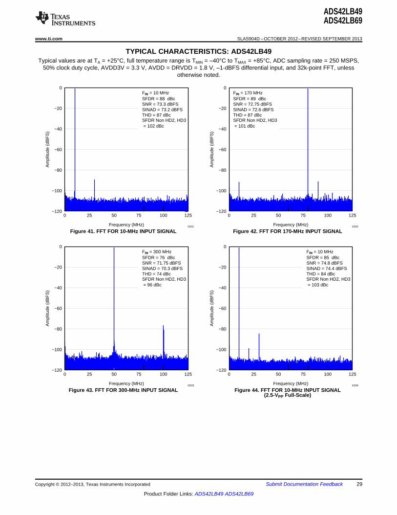
TYPICAL CHARACTERISTICS: ADS42LB49Typical values are at TA = +25°C, full temperature range is TMIN = –40°C to TMAX = +85°C, ADC sampling rate = 250 MSPS,
50% clock duty cycle, AVDD3V = 3.3 V, AVDD = DRVDD = 1.8 V, –1-dBFS differential input, and 32k-point FFT, unlessotherwise noted.
Figure 41. FFT FOR 10-MHz INPUT SIGNAL Figure 42. FFT FOR 170-MHz INPUT SIGNAL
Figure 43. FFT FOR 300-MHz INPUT SIGNAL Figure 44. FFT FOR 10-MHz INPUT SIGNAL(2.5-VPP Full-Scale)
Copyright © 2012–2013, Texas Instruments Incorporated Submit Documentation Feedback 29
Product Folder Links: ADS42LB49 ADS42LB69

−120
−100
−80
−60
−40
−20
0
0 25 50 75 100 125
Frequency (MHz)
Am
plitu
de (
dBF
S)
Each Tone at−7 dBFS AmplitudefIN1 = 46 MHzfIN2 = 50 MHz2−Tone IMD = 99 dBFSSFDR = 103 dBFS
G037
−120
−100
−80
−60
−40
−20
0
0 25 50 75 100 125
Frequency (MHz)
Am
plitu
de (
dBF
S)
Each Tone at−36 dBFS AmplitudefIN1 = 46 MHzfIN2 = 50 MHz2−Tone IMD = 100 dBFSSFDR = 103 dBFS
G038
−120
−100
−80
−60
−40
−20
0
0 25 50 75 100 125
Frequency (MHz)
Am
plitu
de (
dBF
S)
FIN = 170 MHzSFDR = 87 dBcSNR = 74 dBFSSINAD = 73.6 dBFSTHD = 83 dBcSFDR Non HD2, HD3 = 92 dBc
G035
−120
−100
−80
−60
−40
−20
0
0 25 50 75 100 125
Frequency (MHz)
Am
plitu
de (
dBF
S)
FIN = 300 MHzSFDR = 72 dBcSNR = 72.8 dBFSSINAD = 69.5 dBFSTHD = 71 dBcSFDR Non HD2, HD3 = 95 dBc
G036
ADS42LB49ADS42LB69
SLAS904D –OCTOBER 2012–REVISED SEPTEMBER 2013 www.ti.com
TYPICAL CHARACTERISTICS: ADS42LB49 (continued)Typical values are at TA = +25°C, full temperature range is TMIN = –40°C to TMAX = +85°C, ADC sampling rate = 250 MSPS,50% clock duty cycle, AVDD3V = 3.3 V, AVDD = DRVDD = 1.8 V, –1-dBFS differential input, and 32k-point FFT, unlessotherwise noted.
Figure 45. FFT FOR 170-MHz INPUT SIGNAL Figure 46. FFT FOR 300-MHz INPUT SIGNAL(2.5-VPP Full-Scale) (2.5-VPP Full-Scale)
Figure 47. FFT FOR TWO-TONE INPUT SIGNAL Figure 48. FFT FOR TWO-TONE INPUT SIGNAL(At –7 dBFS, 46 MHz and 50 MHz) (At –36 dBFS, 46 MHz and 50 MHz)
30 Submit Documentation Feedback Copyright © 2012–2013, Texas Instruments Incorporated
Product Folder Links: ADS42LB49 ADS42LB69

−108
−106
−104
−102
−100
−98
−96
−94
−36 −33 −30 −27 −24 −21 −18 −15 −12 −9 −7
Each Tone Amplitude (dBFS)
Tw
o −
Ton
e IM
D (
dBF
S)
fIN1 = 46 MHzfIN2 = 50 MHz
G041
−108
−106
−104
−102
−100
−98
−96
−94
−92
−36 −33 −30 −27 −24 −21 −18 −15 −12 −9 −7
Each Tone Amplitude (dBFS)
Tw
o −
Ton
e IM
D (
dBF
S)
fIN1 = 185 MHzfIN2 = 190 MHz
G042
−120
−100
−80
−60
−40
−20
0
0 25 50 75 100 125
Frequency (MHz)
Am
plitu
de (
dBF
S)
Each Tone at−7 dBFS AmplitudefIN1 = 185 MHzfIN2 = 190 MHz2−Tone IMD = 93 dBFSSFDR = 97 dBFS
G039
−120
−100
−80
−60
−40
−20
0
0 25 50 75 100 125
Frequency (MHz)
Am
plitu
de (
dBF
S)
Each Tone at−36 dBFS AmplitudefIN1 = 185 MHzfIN2 = 190 MHz2−Tone IMD = 106dBFSSFDR = 108 dBFS
G040
ADS42LB49ADS42LB69
www.ti.com SLAS904D –OCTOBER 2012–REVISED SEPTEMBER 2013
TYPICAL CHARACTERISTICS: ADS42LB49 (continued)Typical values are at TA = +25°C, full temperature range is TMIN = –40°C to TMAX = +85°C, ADC sampling rate = 250 MSPS,50% clock duty cycle, AVDD3V = 3.3 V, AVDD = DRVDD = 1.8 V, –1-dBFS differential input, and 32k-point FFT, unlessotherwise noted.
Figure 49. FFT FOR TWO-TONE INPUT SIGNAL Figure 50. FFT FOR TWO-TONE INPUT SIGNAL(At –7 dBFS, 185 MHz and 190 MHz) (At –36 dBFS, 185 MHz and 190 MHz)
Figure 51. IMD3 vs INPUT AMPLITUDE Figure 52. IMD3 vs INPUT AMPLITUDE(46 MHz and 50 MHz) (185 MHz and 190 MHz)
Copyright © 2012–2013, Texas Instruments Incorporated Submit Documentation Feedback 31
Product Folder Links: ADS42LB49 ADS42LB69

60
70
80
90
100
110
−2−1.5−1−0.5 0 0.5 1 1.5 2 2.5 3 3.5 4 4.5 5 5.5 6
Gain (dB)
SF
DR
(dB
c)
10 MHz70 MHz130 MHz
170 MHz230 MHz270 MHz
350 MHz400 MHz491 MHz
G045
66
68
70
72
74
76
78
−2−1.5−1−0.5 0 0.5 1 1.5 2 2.5 3 3.5 4 4.5 5 5.5 6
Digital Gain (dB)
SN
R (
dBF
S)
10 MHz70 MHz100 MHz130 MHz
170 MHz230 MHz270 MHz350 MHz
400 MHz491 MHz
G046
55
60
65
70
75
80
85
90
95
100
0 50 100 150 200 250 300 350 400
Input Frequency (MHz)
SF
DR
(dB
c)
2−VPP Full−Scale2.5−VPP Full−Scale
G043
70
71
72
73
74
75
76
77
0 50 100 150 200 250 300 350 400
Input Frequency (MHz)
SN
R (
dBF
S)
2−VPP Full−Scale2.5−VPP Full−Scale
G044
ADS42LB49ADS42LB69
SLAS904D –OCTOBER 2012–REVISED SEPTEMBER 2013 www.ti.com
TYPICAL CHARACTERISTICS: ADS42LB49 (continued)Typical values are at TA = +25°C, full temperature range is TMIN = –40°C to TMAX = +85°C, ADC sampling rate = 250 MSPS,50% clock duty cycle, AVDD3V = 3.3 V, AVDD = DRVDD = 1.8 V, –1-dBFS differential input, and 32k-point FFT, unlessotherwise noted.
Figure 53. SFDR vs INPUT FREQUENCY Figure 54. SNR vs INPUT FREQUENCY
Figure 55. SFDR vs DIGITAL GAIN Figure 56. SNR vs DIGITAL GAIN
32 Submit Documentation Feedback Copyright © 2012–2013, Texas Instruments Incorporated
Product Folder Links: ADS42LB49 ADS42LB69

1.85 1.87 1.9 1.93 1.9582
84
86
89
92
94
96
99
72.5
73
73.5
74
74.5
75
75.5
76
Input Common−Mode Voltage (V)
SF
DR
(dB
c)
SN
R (
dBF
S)
SFDRSNR
Input Frequency = 70 MHz
G017
1.85 1.87 1.9 1.93 1.9580
83
86
89
92
95
98
72
72.5
73
73.5
74
74.5
75
Input Common−Mode Voltage (V)
SF
DR
(dB
c)
SN
R (
dBF
S)
SFDRSNR
Input Frequency = 170 MHz
G050
−70 −60 −50 −40 −30 −20 −10 071.5
72
72.5
73
73.5
74
74.5
75
75.5
76
76.5
77
20
30
40
50
60
70
80
90
100
110
120
130
Amplitude (dBFS)
SN
R (
dBF
S)
SF
DR
(dB
c,dB
FS
)
SNR(dBFS)SFDR(dBc)SFDR(dBFS)
Input Frequency = 70 MHz
G047
−70 −60 −50 −40 −30 −20 −10 071.5
72
72.5
73
73.5
74
74.5
75
75.5
76
76.5
77
20
30
40
50
60
70
80
90
100
110
120
130
Amplitude (dBFS)S
NR
(dB
FS
)
SF
DR
(dB
c,dB
FS
)
SNR(dBFS)SFDR(dBc)SFDR(dBFS)
Input Frequency = 170 MHz
G048
ADS42LB49ADS42LB69
www.ti.com SLAS904D –OCTOBER 2012–REVISED SEPTEMBER 2013
TYPICAL CHARACTERISTICS: ADS42LB49 (continued)Typical values are at TA = +25°C, full temperature range is TMIN = –40°C to TMAX = +85°C, ADC sampling rate = 250 MSPS,50% clock duty cycle, AVDD3V = 3.3 V, AVDD = DRVDD = 1.8 V, –1-dBFS differential input, and 32k-point FFT, unlessotherwise noted.
Figure 57. PERFORMANCE ACROSS INPUT AMPLITUDE Figure 58. PERFORMANCE ACROSS INPUT AMPLITUDE(170 MHz)(70 MHz)
Figure 59. PERFORMANCE vs INPUT COMMON-MODE Figure 60. PERFORMANCE vs INPUT COMMON-MODEVOLTAGE (70 MHz) VOLTAGE (170 MHz)
Copyright © 2012–2013, Texas Instruments Incorporated Submit Documentation Feedback 33
Product Folder Links: ADS42LB49 ADS42LB69

75
78
81
84
87
90
93
96
99
102
−40 −15 10 35 60 85Temperature (°C)
SF
DR
(dB
c)
AVDD3V = 3.15 VAVDD3V = 3.2 VAVDD3V = 3.25 VAVDD3V = 3.3 V
AVDD3V = 3.35 VAVDD3V = 3.4 VAVDD3V = 3.45 V
Input Frequency = 170 MHz
G053
71.5
72
72.5
73
73.5
74
74.5
−40 −15 10 35 60 85Temperature (°C)
SN
R (
dBF
S)
AVDD3V = 3.15 VAVDD3V = 3.2 VAVDD3V = 3.25 VAVDD3V = 3.3 V
AVDD3V = 3.35 VAVDD3V = 3.4 VAVDD3V = 3.45 V
Input Frequency = 170 MHz
G054
78
81
84
87
90
93
96
99
−40 −15 10 35 60 85Temperature (°C)
SF
DR
(dB
c)
AVDD = 1.7 VAVDD = 1.75 VAVDD = 1.8 V
AVDD = 1.85 VAVDD = 1.9 V
Input Frequency = 170 MHz
G051
71.5
72
72.5
73
73.5
74
74.5
75
−40 −15 10 35 60 85Temperature (°C)
SN
R (
dBF
S)
AVDD = 1.7 VAVDD = 1.75VAVDD = 1.8 V
AVDD = 1.85 VAVDD = 1.9 V
Input Frequency = 170 MHz
G052
ADS42LB49ADS42LB69
SLAS904D –OCTOBER 2012–REVISED SEPTEMBER 2013 www.ti.com
TYPICAL CHARACTERISTICS: ADS42LB49 (continued)Typical values are at TA = +25°C, full temperature range is TMIN = –40°C to TMAX = +85°C, ADC sampling rate = 250 MSPS,50% clock duty cycle, AVDD3V = 3.3 V, AVDD = DRVDD = 1.8 V, –1-dBFS differential input, and 32k-point FFT, unlessotherwise noted.
Figure 61. SFDR vs AVDD SUPPLY AND TEMPERATURE Figure 62. SNR vs AVDD SUPPLY AND TEMPERATURE(170 MHz) (170 MHz)
Figure 63. SFDR vs AVDD_BUF SUPPLY AND Figure 64. SNR vs AVDD_BUF SUPPLY ANDTEMPERATURE (170 MHz) TEMPERATURE (170 MHz)
34 Submit Documentation Feedback Copyright © 2012–2013, Texas Instruments Incorporated
Product Folder Links: ADS42LB49 ADS42LB69
0.1 0.3 0.5 0.7 0.9 1.1 1.3 1.5 1.7 1.9 2.184
86
88
90
92
94
96
71
72
73
74
75
76
77
Differential Clock Amplitudes (Vpp)
SF
DR
(dB
c)
SN
R (
dBF
S)
SFDRSNR
Input Frequency = 70 MHz
G057
0.1 0.3 0.5 0.7 0.9 1.1 1.3 1.5 1.7 1.9 2.184
86
88
90
92
94
68
70
72
74
76
78
Differential Clock Amplitudes (Vpp)
SF
DR
(dB
c)
SN
R (
dBF
S)
SFDRSNR
Input Frequency = 170 MHz
G058
84
85
86
87
88
89
90
91
92
−40 −15 10 35 60 85Temperature (°C)
SF
DR
(dB
c)
DRVDD = 1.7 VDRVDD = 1.75 VDRVDD = 1.8 V
DRVDD = 1.85 VDRVDD = 1.9 V
Input Frequency = 170 MHz
G055
71.5
72
72.5
73
73.5
74
74.5
75
−40 −15 10 35 60 85Temperature (°C)
SN
R (
dBF
S)
DRVDD = 1.7 VDRVDD = 1.75 VDRVDD = 1.8 V
DRVDD = 1.85 VDRVDD = 1.9 V
Input Frequency = 170 MHz
G056
ADS42LB49ADS42LB69
www.ti.com SLAS904D –OCTOBER 2012–REVISED SEPTEMBER 2013
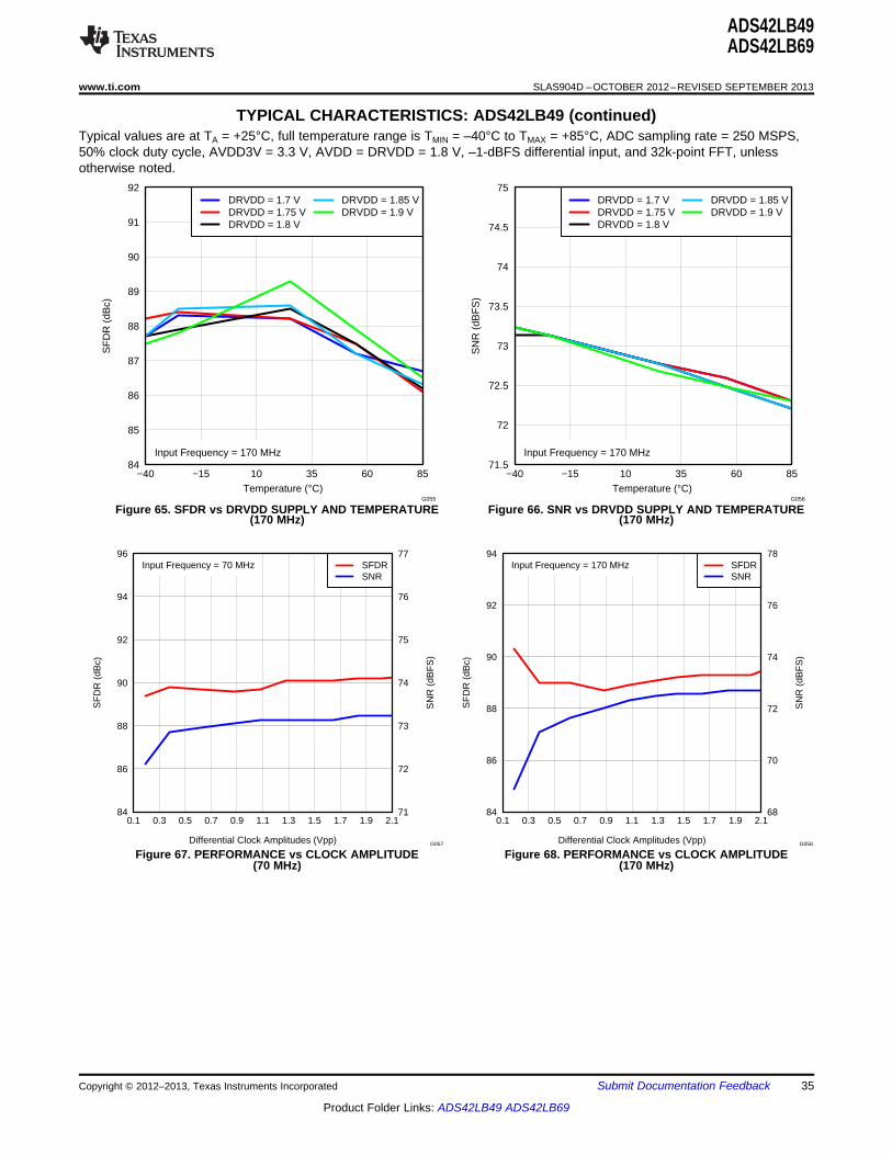
TYPICAL CHARACTERISTICS: ADS42LB49 (continued)Typical values are at TA = +25°C, full temperature range is TMIN = –40°C to TMAX = +85°C, ADC sampling rate = 250 MSPS,50% clock duty cycle, AVDD3V = 3.3 V, AVDD = DRVDD = 1.8 V, –1-dBFS differential input, and 32k-point FFT, unlessotherwise noted.
Figure 65. SFDR vs DRVDD SUPPLY AND TEMPERATURE Figure 66. SNR vs DRVDD SUPPLY AND TEMPERATURE(170 MHz) (170 MHz)
Figure 67. PERFORMANCE vs CLOCK AMPLITUDE Figure 68. PERFORMANCE vs CLOCK AMPLITUDE(70 MHz) (170 MHz)
Copyright © 2012–2013, Texas Instruments Incorporated Submit Documentation Feedback 35
Product Folder Links: ADS42LB49 ADS42LB69

30 40 50 60 7082
84
86
88
90
92
94
96
71
72
73
74
75
76
77
78
Input Clock Duty Cycle (%)
SF
DR
(dB
c)
SN
R (
dBF
S)
SNRSFDR
Input Frequency = 70 MHz
G059
30 40 50 60 7082
84
86
88
90
92
94
96
70
71
72
73
74
75
76
77
Input Clock Duty Cycle (%)S
FD
R (
dBc)
SN
R (
dBF
S)
SNRSFDR
Input Frequency = 170 MHz
G060
ADS42LB49ADS42LB69
SLAS904D –OCTOBER 2012–REVISED SEPTEMBER 2013 www.ti.com
TYPICAL CHARACTERISTICS: ADS42LB49 (continued)Typical values are at TA = +25°C, full temperature range is TMIN = –40°C to TMAX = +85°C, ADC sampling rate = 250 MSPS,50% clock duty cycle, AVDD3V = 3.3 V, AVDD = DRVDD = 1.8 V, –1-dBFS differential input, and 32k-point FFT, unlessotherwise noted.
Figure 69. PERFORMANCE vs CLOCK DUTY CYCLE Figure 70. PERFORMANCE vs CLOCK DUTY CYCLE(70 MHz) (170 MHz)
36 Submit Documentation Feedback Copyright © 2012–2013, Texas Instruments Incorporated
Product Folder Links: ADS42LB49 ADS42LB69

−120
−100
−80
−60
−40
−20
0
0 25 50 75 100 125
Frequency (MHz)
Am
plitu
de (
dBF
S)
fIN = 20 MHzSFDR = 89 dBcfPSRR = 4 MHz50 − mVPPAmplitude(fIN) = −1 dBFSAmplitude(fPSRR) = −104 dBFSAmplitude(fIN + fPSRR) = −93 dBFSAmplitude(fIN − fPSRR) = −95 dBFS
G063
−90
−80
−70
−60
−50
−40
−30
−20
0 50 100 150 200 250 300
Test Signal Frequency on Supply (MHz)
PS
RR
(dB
)
50−mVPP Signal Superimposed on AVDD100−mVPP Signal Superimposed on AVDD3V
Input Frequency = 20MHz
G064
−120
−100
−80
−60
−40
−20
0
0 25 50 75 100 125
Frequency (MHz)
Am
plitu
de (
dBF
S)
fIN = 100 MHzSFDR = 82 dBcfCM = 5 MHz50 − mVPPAmplitude(fIN) = −1 dBFSAmplitude(fCM) = −83 dBFSAmplitude(fIN + fCM) = −90 dBFSAmplitude(fIN − fCM) = −86 dBFS
G061
−65
−60
−55
−50
−45
−40
−35
−30
−25
−20
−15
−10
−5
0
0 50 100 150 200 250 300
Common−Mode Test Signal Frequency (MHz)
CM
RR
(dB
)
Input Frequency = 10MHz 50−mVPP Signal Superimposed on VCM
G062
ADS42LB49ADS42LB69
www.ti.com SLAS904D –OCTOBER 2012–REVISED SEPTEMBER 2013
TYPICAL CHARACTERISTICS: CommonTypical values are at TA = +25°C, full temperature range is TMIN = –40°C to TMAX = +85°C, ADC sampling rate = 250 MSPS,
50% clock duty cycle, AVDD3V = 3.3 V, AVDD = DRVDD = 1.8 V, –1-dBFS differential input, and 32k-point FFT, unlessotherwise noted.
Figure 71. CMRR FFT Figure 72. CMRR vs TEST SIGNAL FREQUENCY
Figure 73. PSRR FFT FOR AVDD SUPPLY Figure 74. PSRR vs TEST SIGNAL FREQUENCY
Copyright © 2012–2013, Texas Instruments Incorporated Submit Documentation Feedback 37
Product Folder Links: ADS42LB49 ADS42LB69

0
0.2
0.4
0.6
0.8
1
1.2
1.4
1.6
1.8
2
0 50 100 150 200 250
Sampling Speed (MSPS)
Tot
al P
ower
(W
)
AVDD PowerDRVDD PowerAVDD3V PowerTotal Power
G065
ADS42LB49ADS42LB69
SLAS904D –OCTOBER 2012–REVISED SEPTEMBER 2013 www.ti.com
TYPICAL CHARACTERISTICS: Common (continued)Typical values are at TA = +25°C, full temperature range is TMIN = –40°C to TMAX = +85°C, ADC sampling rate = 250 MSPS,50% clock duty cycle, AVDD3V = 3.3 V, AVDD = DRVDD = 1.8 V, –1-dBFS differential input, and 32k-point FFT, unlessotherwise noted.
Figure 75. TOTAL POWER vs SAMPLING FREQUENCY
38 Submit Documentation Feedback Copyright © 2012–2013, Texas Instruments Incorporated
Product Folder Links: ADS42LB49 ADS42LB69

70
70
70
75
75
75
80
80
80
85
85
85
90
90
90
95
9595
Input Frequency, MHz
Sam
plin
g F
requ
ency
, MS
PS
100 200 300 400 500 60080
100
120
140
160
180
200
220
240
70 75 80 85 90 95
67
67
67
71
71
71
75
75
75
79
79
79
83
83
83
87
87
87
91
91
91
91
91
91
87
87
Input Frequency, MHz
Sam
plin
g F
requ
ency
, MS
PS
50 100 150 200 250 300 350 40080
100
120
140
160
180
200
220
240
65 70 75 80 85 90
ADS42LB49ADS42LB69
www.ti.com SLAS904D –OCTOBER 2012–REVISED SEPTEMBER 2013
TYPICAL CHARACTERISTICS: ContourTypical values are at TA = +25°C, full temperature range is TMIN = –40°C to TMAX = +85°C, ADC sampling rate = 250 MSPS,
50% clock duty cycle, AVDD3V = 3.3 V, AVDD = DRVDD = 1.8 V, –1-dBFS differential input, and 65k-point FFT, unlessotherwise noted.
Spurious-Free Dynamic Range (SFDR): General
Figure 76. SFDR (0-dB Gain)
Figure 77. SFDR (6-dB Gain)
Copyright © 2012–2013, Texas Instruments Incorporated Submit Documentation Feedback 39
Product Folder Links: ADS42LB49 ADS42LB69

65.566
66.5
66.5
66.5
67
67
67
67.5
67.5
67.5
67.75
67.75
67.75
68
68
68
Input Frequency, MHz
Sam
plin
g F
requ
ency
, MS
PS
100 200 300 400 500 60080
100
120
140
160
180
200
220
240
65 65.5 66 66.5 67 67.5 68
7070.5
71
71
71
71.5
71.5
71.5
72
72
72
72.5
72.5
72.5
73
73
73
73.5
73.5
73.574
Input Frequency, MHz
Sam
plin
g F
requ
ency
, MS
PS
50 100 150 200 250 300 350 40080
100
120
140
160
180
200
220
240
69.5 70 70.5 71 71.5 72 72.5 73 73.5 74
ADS42LB49ADS42LB69
SLAS904D –OCTOBER 2012–REVISED SEPTEMBER 2013 www.ti.com
TYPICAL CHARACTERISTICS: Contour (continued)Typical values are at TA = +25°C, full temperature range is TMIN = –40°C to TMAX = +85°C, ADC sampling rate = 250 MSPS,50% clock duty cycle, AVDD3V = 3.3 V, AVDD = DRVDD = 1.8 V, –1-dBFS differential input, and 65k-point FFT, unlessotherwise noted.Signal-to-Noise Ratio (SNR): ADS42LB69
Figure 78. SNR (0-dB Gain, 16 Bits)
Figure 79. SNR (6-dB Gain, 16 Bits)
40 Submit Documentation Feedback Copyright © 2012–2013, Texas Instruments Incorporated
Product Folder Links: ADS42LB49 ADS42LB69

65.5
66
66
66
66.5
66.5
66.5
67
67
67
67.25
67.25
67.25
67.5
67.5
67.5
67.75
67.75
67.75
Input Frequency, MHz
Sam
plin
g F
requ
ency
, MS
PS
50 100 150 200 250 300 350 400 450 500 550 60080
100
120
140
160
180
200
220
240
65 65.5 66 66.5 67 67.5
70
70.5
70.5
71
71
71
71.5
71.5
71.5
72
72
72
72.5
72.5
72.5
73
73
7373.5
Input Frequency, MHz
Sam
plin
g F
requ
ency
, MS
PS
50 100 150 200 250 300 350 40080
100
120
140
160
180
200
220
240
69.5 70 70.5 71 71.5 72 72.5 73 73.5
ADS42LB49ADS42LB69
www.ti.com SLAS904D –OCTOBER 2012–REVISED SEPTEMBER 2013
TYPICAL CHARACTERISTICS: Contour (continued)Typical values are at TA = +25°C, full temperature range is TMIN = –40°C to TMAX = +85°C, ADC sampling rate = 250 MSPS,50% clock duty cycle, AVDD3V = 3.3 V, AVDD = DRVDD = 1.8 V, –1-dBFS differential input, and 65k-point FFT, unlessotherwise noted.Signal-to-Noise Ratio (SNR): ADS42LB49
Figure 80. SNR (0-dB Gain, 14 Bits)
Figure 81. SNR (6-dB Gain, 14 Bits)
Copyright © 2012–2013, Texas Instruments Incorporated Submit Documentation Feedback 41
Product Folder Links: ADS42LB49 ADS42LB69

ADS42LB49ADS42LB69
SLAS904D –OCTOBER 2012–REVISED SEPTEMBER 2013 www.ti.com
DEVICE CONFIGURATION
The ADS42LB49 and ADS42LB69 can be configured using a serial programming interface, as described in thissection. In addition, the device has two bidirectional parallel pins (CTRL1 and CTRL2). By default, these pins actas input pins and control the power-down modes, as described in Table 5 and Table 6. These pins can beprogrammed as output pins that deliver overrange information by setting the PDN/OVR_FOR_CTRL_PINSregister bit.
Table 5. PDN/OVR_FOR_CTRL_PINS Bit (Set to '0')CTRL2 CTRL1 PIN DIRECTION FUNCTION
Low Low Input Default operationLow High Input Channel A power-down
Channel B powers down in QDR mode. Do not use inHigh Low Input DDR mode.High High Input Channels A and B power-down
Table 6. PDN/OVR_FOR_CTRL_PINS Bit (Set to '1')CTRL2 CTRL1 PIN DIRECTION
Carries OVR for channel B Carries OVR for channel A Output
DETAILS OF SERIAL INTERFACEThe ADC has a set of internal registers that can be accessed by the serial interface formed by the SEN (serialinterface enable), SCLK (serial interface clock), SDATA (serial interface data) and SDOUT (serial interface dataoutput) pins. Serial shift of bits into the device is enabled when SEN is low. Serial data SDATA are latched atevery SCLK rising edge when SEN is active (low). The serial data are loaded into the register at every 16thSCLK rising edge when SEN is low. When the word length exceeds a multiple of 16 bits, the excess bits areignored. Data can be loaded in multiples of 16-bit words within a single active SEN pulse. The interface can workwith SCLK frequencies from 20 MHz down to very low speeds (of a few hertz) and also with non-50% SCLK dutycycle.
42 Submit Documentation Feedback Copyright © 2012–2013, Texas Instruments Incorporated
Product Folder Links: ADS42LB49 ADS42LB69

Power SupplyAVDD, AVDD3V, DRVDD
RESET
SEN
t1
t2 t3
ADS42LB49ADS42LB69
www.ti.com SLAS904D –OCTOBER 2012–REVISED SEPTEMBER 2013
Register InitializationAfter power-up, the internal registers must be initialized to their default values through a hardware reset byapplying a high pulse on the RESET pin (of widths greater than 10 ns), as shown in Figure 82 and Table 7. Ifrequired, serial interface registers can later be cleared during operation by:1. Either through a hardware reset or2. By applying a software reset. When using the serial interface, set the RESET bit (D0 in register address 08h)
high. This setting initializes the internal registers to the default values and then self-resets the RESET bit low.In this case, the RESET pin is kept low.
NOTE: After power-up, the internal registers must be initialized to their default values through a hardware reset by applying a high pulse onthe RESET pin.
Figure 82. Reset Timing Diagram
Table 7. Reset Timing (1)
PARAMETER CONDITIONS MIN TYP MAX UNITt1 Power-on delay Delay from AVDD and DRVDD power-up to active RESET pulse 1 ms
10 nst2 Reset pulse width Active RESET signal pulse width
1 µst3 Register write delay Delay from RESET disable to SEN active 100 ns
(1) Typical values at +25°C; minimum and maximum values across the full temperature range: TMIN = –40°C to TMAX = +85°C, unlessotherwise noted.
Copyright © 2012–2013, Texas Instruments Incorporated Submit Documentation Feedback 43
Product Folder Links: ADS42LB49 ADS42LB69

R/W A5 A4 A3 A2 A1 A0 D7 D6 D5 D4 D3 D2 D1 D0
Register Address <5:0> Register Data <7:0>
SDATA
SCLK
tSCLK tDSU
tDH
SEN
tSLOADS tSLOADH
RESET
0
= 0
ADS42LB49ADS42LB69
SLAS904D –OCTOBER 2012–REVISED SEPTEMBER 2013 www.ti.com
Serial Register WriteThe internal register of the ADS42LB49 and ADS42LB69 can be programmed following these steps:1. Drive SEN pin low2. Set the R/W bit to ‘0’ (bit A7 of the 8 bit address)3. Set bit A6 in the address field to ‘0’4. Initiate a serial interface cycle specifying the address of the register (A5 to A0) whose content must be
written5. Write 8 bit data which is latched in on the rising edge of SCLK.
Figure 83 and Table 8 illustrate these steps.
Figure 83. Serial Register Write Timing Diagram
Table 8. Serial Interface Timing (only when Serial Interface is Used) (1)
PARAMETER MIN TYP MAX UNITfSCLK SCLK frequency (equal to 1 / tSCLK) > dc 20 MHztSLOADS SEN to SCLK setup time 25 nstSLOADH SCLK to SEN hold time 25 nstDSU SDIO setup time 25 nstDH SDIO hold time 25 ns
(1) Typical values are at +25°C; minimum and maximum values across the full temperature range: TMIN = –40°C to TMAX = +85°C, AVDD3V= 3.3 V, and AVDD = DRVDD = 1.8 V, unless otherwise noted.
44 Submit Documentation Feedback Copyright © 2012–2013, Texas Instruments Incorporated
Product Folder Links: ADS42LB49 ADS42LB69
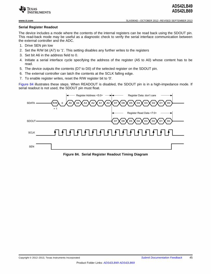
R/W A5 A4 A3 A2 A1 A0 D7 D6 D5 D4 D3 D2 D1 D0
Register Address <5:0> Register Data: don’t care
SDATA
SCLK
SEN
0
SDOUT D7 D6 D5 D4 D3 D2 D1 D0
Register Read Data <7:0>
= 1
ADS42LB49ADS42LB69
www.ti.com SLAS904D –OCTOBER 2012–REVISED SEPTEMBER 2013
Serial Register ReadoutThe device includes a mode where the contents of the internal registers can be read back using the SDOUT pin.This read-back mode may be useful as a diagnostic check to verify the serial interface communication betweenthe external controller and the ADC.1. Drive SEN pin low2. Set the R/W bit (A7) to '1'. This setting disables any further writes to the registers3. Set bit A6 in the address field to 0.4. Initiate a serial interface cycle specifying the address of the register (A5 to A0) whose content has to be
read.5. The device outputs the contents (D7 to D0) of the selected register on the SDOUT pin.6. The external controller can latch the contents at the SCLK falling edge.7. To enable register writes, reset the R/W register bit to '0'.
Figure 84 illustrates these steps. When READOUT is disabled, the SDOUT pin is in a high-impedance mode. Ifserial readout is not used, the SDOUT pin must float.
Figure 84. Serial Register Readout Timing Diagram
Copyright © 2012–2013, Texas Instruments Incorporated Submit Documentation Feedback 45
Product Folder Links: ADS42LB49 ADS42LB69

ADS42LB49ADS42LB69
SLAS904D –OCTOBER 2012–REVISED SEPTEMBER 2013 www.ti.com
SUMMARY OF SERIAL INTERFACE REGISTERS
REGISTER REGISTER DATAADDRESSA7–A0 IN D7 D6 D5 D4 D3 D2 D1 D0HEX
6 1 0 0 0 0 0 CLK DIV7 0 0 0 0 0 SYNCIN DELAY
DATA DIS CTRL TEST PAT8 PDN CHA PDN CHB STDBY 0 RESETFORMAT PINS ALIGNCHA GAINB CHA GAIN 0 FLIP DATAENCHB GAINC CHBGAIN OVR ON LSBEN
FAST OVRD 0 1 1 0 1 1 0 ON PINF CHA TEST PATTERNS CHB TEST PATTERNS10 CUSTOM PATTERN 1 (15:8)11 CUSTOM PATTERN 1 (7:0)12 CUSTOM PATTERN 2 (15:8)13 CUSTOM PATTERN 2 (7:0)
DISABLELVDS CLK LVDS DATA DISABLE14 0 0 0 0 OUTPUTSTRENGTH STRENGTH OUTPUT CHBCHA15 0 0 0 0 0 0 0 DDR - QDR16 0 0 DDR OUTPUT TIMING 0
LVDS CLK INV CLK OUT17 STRENGTH 0 QDR TIMING CHA CHAENINV CLK OUT18 0 0 QDR TIMING CHB CHB
Always write1F FAST OVR THRESHOLD'0'PDN/OVR
20 0 0 0 0 0 0 0 FOR CTRLPINS
46 Submit Documentation Feedback Copyright © 2012–2013, Texas Instruments Incorporated
Product Folder Links: ADS42LB49 ADS42LB69

ADS42LB49ADS42LB69
www.ti.com SLAS904D –OCTOBER 2012–REVISED SEPTEMBER 2013
DESCRIPTION OF SERIAL INTERFACE REGISTERSREGISTER REGISTER DATAADDRESS
A7-A0 IN HEX D7 D6 D5 D4 D3 D2 D1 D06 1 0 0 0 0 0 CLK DIV
Default: 80hD[1:0] CLK DIV Internal clock divider for input sample clock00 Divide-by-1 (clock divider bypassed)01 Divide-by-210 Divide-by-111 Divide-by-4
REGISTER REGISTER DATAADDRESSA7-A0 IN HEX D7 D6 D5 D4 D3 D2 D1 D0
7 0 0 0 0 0 SYNCIN DELAY
Default: 00hControls the delay of the SYNCIN input with respect to the input clock.D[2:0] SYNCIN DELAY Typical values for the expected delay of different settings are:
000 0-ps delay 100 240-ps delay001 60-ps delay 101 300-ps delay010 120-ps delay 110 360-ps delay011 180-ps delay 111 420-ps delay
Copyright © 2012–2013, Texas Instruments Incorporated Submit Documentation Feedback 47
Product Folder Links: ADS42LB49 ADS42LB69

ADS42LB49ADS42LB69
SLAS904D –OCTOBER 2012–REVISED SEPTEMBER 2013 www.ti.com
REGISTER REGISTER DATAADDRESSA7-A0 IN HEX D7 D6 D5 D4 D3 D2 D1 D0
DATA DIS CTRL TEST PAT8 PDN CHA PDN CHB STDBY 0 RESETFORMAT PINS ALIGN
Default: 00hPDN CHA and PDND[7:6] Power-down channels A and B. Effective only when bit DIS CTRL PINS is set to '1'.CHB
00 Normal operation01 Channel B powers down. Use only if the QDR interface is selected. Do not use in the DDR interface.10 Channel A powers down. Functions in both QDR and DDR interfaces.11 Both channels power down. Functions in both QDR and DDR interfaces.
D5 STDBY Dual ADC is placed into standby mode0 Normal operation1 Power down
D4 DATA FORMAT Digital output data format0 Twos complement1 Offset binary
Disables power-down control from CTRL1, CTRL2 pins. This bit also functions as an enable bit for theD3 DIS CTRL PINS INV CLK OUT CHA, INV CLK OUT CHB, and DDR OUTPUT TIMING bits.0 CTRL1 and CTRL2 pins control power-down options for channels A and B
Register bits PDN CHA and PDN CHB determine power-down options for channels A and B. Register bits INV CLK OUT1 CHA, INV CLK OUT CHB, and DDR OUTPUT TIMING become effective.
D2 TEST PAT ALIGN Aligns test patterns of two channels0 Test patterns for channel A and channel B are free running1 Test patterns for both channels are synchronized
D0 RESET Software reset appliedThis bit resets all internal registers to the default values and self-clears to ‘0’
48 Submit Documentation Feedback Copyright © 2012–2013, Texas Instruments Incorporated
Product Folder Links: ADS42LB49 ADS42LB69

ADS42LB49ADS42LB69
www.ti.com SLAS904D –OCTOBER 2012–REVISED SEPTEMBER 2013
REGISTER REGISTER DATAADDRESSA7-A0 IN HEX D7 D6 D5 D4 D3 D2 D1 D0
B CHA GAIN CHA GAIN EN 0 FLIP DATA
Default: 00hD[7:3] CHA GAIN Digital gain for channel A. Effective when register bit CHA GAIN EN is set to '1'. Bit descriptions are
listed in Table 9.
Table 9. Digital Gain for Channel ADIGITAL GAIN FOR MAX INPUT DIGITAL GAIN FOR MAX INPUTDIGITAL GAIN (dB) DIGITAL GAIN (dB)CHANNEL A VOLTAGE (VPP) CHANNEL A VOLTAGE (VPP)
00000 0 2.0 01010 1.5 1.700001 Do not use — 01011 2 1.600010 Do not use — 01100 2.5 1.500011 –2.0 2.5 01101 3 1.400100 –1.5 2.4 01110 3.5 1.300101 –1.0 2.2 01111 4 1.2500110 –0.5 2.1 10000 4.5 1.200111 0 2.0 10001 5 1.101000 0.5 1.9 10010 5.5 1.0501001 1 1.8 10011 6 1.0
D2 CHA GAIN EN Digital gain enable bit for channel A0 Digital gain disabled1 Digital gain enabled
D0 FLIP DATA Flips bit order on LVDS output bus (LSB versus MSB)0 Normal operation1 Output bus flipped. In the ADS42LB69, output data bit D0 becomes D15, D1 becomes D14, and so forth.
In the ADS42LB49, output data bit D0 becomes D13, D1 becomes D12, and so forth.
Copyright © 2012–2013, Texas Instruments Incorporated Submit Documentation Feedback 49
Product Folder Links: ADS42LB49 ADS42LB69

ADS42LB49ADS42LB69
SLAS904D –OCTOBER 2012–REVISED SEPTEMBER 2013 www.ti.com
REGISTER REGISTER DATAADDRESSA7-A0 IN HEX D7 D6 D5 D4 D3 D2 D1 D0
CHB GAINC CHB GAIN OVR ON LSBEN
Default: 00hD[7:3] CHB GAIN Digital gain for channel B. Effective when register bit CHB GAIN EN is set to '1'.Bit descriptions are
listed in Table 10.
Table 10. Digital Gain for Channel BDIGITAL GAIN FOR MAX INPUT DIGITAL GAIN FOR MAX INPUTDIGITAL GAIN (dB) DIGITAL GAIN (dB)CHANNEL B VOLTAGE (VPP) CHANNEL B VOLTAGE (VPP)
00000 0 2.0 01010 1.5 1.700001 Do not use — 01011 2 1.600010 Do not use — 01100 2.5 1.500011 –2.0 2.5 01101 3 1.400100 –1.5 2.4 01110 3.5 1.300101 –1.0 2.2 01111 4 1.2500110 –0.5 2.1 10000 4.5 1.200111 0 2.0 10001 5 1.101000 0.5 1.9 10010 5.5 1.0501001 1 1.8 10011 6 1.0
D2 CHB GAIN EN Digital gain enable bit for channel B0 Digital gain disabled1 Digital gain disabled
D[1:0] OVR ON LSB Functions only with the DDR interface option. Replaces the LSB pair of 16-bit data (D1, D0) with OVRinformation. See the Overrange Indication section.
00 D1 and D0 are output in the ADS42LB69, NC for the ADS42LB4901 Fast OVR in LVDS logic level10 Normal OVR in LVDS logic level11 D1 and D0 are output in the ADS42LB69, NC for the ADS42LB49
REGISTER REGISTER DATAADDRESSA7-A0 IN HEX D7 D6 D5 D4 D3 D2 D1 D0
FAST OVRD 0 1 1 0 1 1 0 ON PIN
Default:6ChD0 FAST OVR ON Determines whether normal OVR or fast OVR information is brought on the OVRx, CTRL1, and CTRL2
PIN pins. See the Overrange Indication section.0 Normal OVR available on the OVRx, CTRL1, and CTRL2 pins1 Fast OVR available on the OVRx, CTRL1, and CTRL2 pins
50 Submit Documentation Feedback Copyright © 2012–2013, Texas Instruments Incorporated
Product Folder Links: ADS42LB49 ADS42LB69

ADS42LB49ADS42LB69
www.ti.com SLAS904D –OCTOBER 2012–REVISED SEPTEMBER 2013
REGISTER REGISTER DATAADDRESSA7-A0 IN HEX D7 D6 D5 D4 D3 D2 D1 D0
F CHA TEST PATTERNS CHB TEST PATTERNS
Default: 00hD[7:4] CHA TEST PATTERNS Channel A test pattern programmability0000 Normal Operation0001 Outputs all 0s0010 Outputs all 1s
In the ADS42LB69, data are an alternating sequence of 1010101010101010 and0011 Outputs toggle pattern: 0101010101010101.
In the ADS42LB49, data alternate between 10101010101010 and 01010101010101.In the ADS42LB69, data increment by 1 LSB every clock cycle from code 0 to 65535.0100 Output digital ramp: In the ADS42LB49 data increment by 1 LSB every fourth clock cycle from code 0 to 16383.
0101 Increment pattern: Do not useIn the ADS42LB69, data are the same as programmed by registers bits CUSTOM PATTERN1[15:0].0110 Single pattern: In the ADS42LB49, data are the same as programmed by register bits CUSTOM PATTERN1[15:2].In the ADS42LB69, data alternate between CUSTOM PATTERN 1[15:0] and CUSTOM PATTERN2[15:0].0111 Double pattern: In the ADS42LB49 data alternate between CUSTOM PATTERN 1[15:2] and CUSTOM PATTERN2[15:2].
1000 Deskew pattern: In the ADS42LB69, data are AAAAh. In the ADS42LB49, data are 3AAAh.1001 Do not use1010 PRBS pattern: Data are a sequence of pseudo-random numbers
In the ADS42LB69, data are a repetitive sequence of the following eight numbers, forming a sine-wave in twos complement format: 1, 9598, 32768, 55938, 65535, 55938, 32768, and 9598.1011 8P sine: In the ADS42LB49, data are a repetitive sequence of the following eight numbers, forming a sine-wave in twos complement format: 0, 2399, 8192, 13984, 16383, 13984, 8192, and 2399.
D[3:0] CHB TEST PATTERNS Channel B test pattern programmability0000 Normal Operation0001 Outputs all 0s0010 Outputs all 1s
In the ADS42LB69, data are an alternating sequence of 1010101010101010 and0011 Outputs toggle pattern: 0101010101010101.
In the ADS42LB49, data alternate between 10101010101010 and 01010101010101.In the ADS42LB69, data increment by 1 LSB every clock cycle from code 0 to 65535.0100 Output digital ramp: In the ADS42LB49 data increment by 1 LSB every fourth clock cycle from code 0 to 16383.
0101 Increment pattern: Do not useIn the ADS42LB69, data are the same as programmed by registers bits CUSTOM PATTERN1[15:0].0110 Single pattern: In the ADS42LB49, data are the same as programmed by register bits CUSTOM PATTERN1[15:2].In the ADS42LB69, data alternate between CUSTOM PATTERN 1[15:0] and CUSTOM PATTERN2[15:0].0111 Double pattern: In the ADS42LB49 data alternate between CUSTOM PATTERN 1[15:2] and CUSTOM PATTERN2[15:2].
1000 Deskew pattern: In the ADS42LB69, data are AAAAh. In the ADS42LB49, data are 3AAAh.1001 Do not use1010 PRBS pattern: Data are a sequence of pseudo-random numbers
In the ADS42LB69, data are a repetitive sequence of the following eight numbers, forming a sine-wave in twos complement format: 1, 9598, 32768, 55938, 65535, 55938, 32768, and 9598.1011 8P sine: In the ADS42LB49, data are a repetitive sequence of the following eight numbers, forming a sine-wave in twos complement format: 0, 2399, 8192, 13984, 16383, 13984, 8192, and 2399.
Copyright © 2012–2013, Texas Instruments Incorporated Submit Documentation Feedback 51
Product Folder Links: ADS42LB49 ADS42LB69

ADS42LB49ADS42LB69
SLAS904D –OCTOBER 2012–REVISED SEPTEMBER 2013 www.ti.com
REGISTER REGISTER DATAADDRESSA7-A0 IN HEX D7 D6 D5 D4 D3 D2 D1 D0
10 CUSTOM PATTERN 1 (15:8)
Default: 00hD[7:0] CUSTOM PATTERN 1 (15:8) Sets the custom pattern 1[15:8] with these bits for both channels
REGISTER REGISTER DATAADDRESSA7-A0 IN HEX D7 D6 D5 D4 D3 D2 D1 D0
11 CUSTOM PATTERN 1 (7:0)
Default: 00hD[7:0] CUSTOM PATTERN 1 (7:0) Sets the custom pattern 1[7:0] with these bits for both channels
REGISTER REGISTER DATAADDRESSA7-A0 IN HEX D7 D6 D5 D4 D3 D2 D1 D0
12 CUSTOM PATTERN 2 (15:8)
Default: 00hD[7:0] CUSTOM PATTERN 2 (15:8) Sets the custom pattern 2[15:8] with these bits for both channels
REGISTER REGISTER DATAADDRESSA7-A0 IN HEX D7 D6 D5 D4 D3 D2 D1 D0
13 CUSTOM PATTERN 2 (7:0)
Default: 00hD[7:0] CUSTOM PATTERN 2 (7:0) Sets the custom pattern 2[7:0] with these bits for both channels
REGISTER REGISTER DATAADDRESSA7-A0 IN HEX D7 D6 D5 D4 D3 D2 D1 D0
DISABLE DISABLELVDS CLK LVDS DATA14 0 0 0 0 OUTPUT OUTPUTSTRENGTH STRENGTH CHA CHB
Default: 00hD3 LVDS CLK STRENGTH Increases the LVDS drive strength of the CLKOUTP, CLKOUTM buffers in the DDR pinout and
the DxCLKP, DxCLKM buffers in the QDR pinout0 LVDS output clock buffer at default strength used with 100-Ω external termination1 LVDS output clock buffer has double strength used with 50-Ω external termination. Effective only when bit LVDS CLK
STRENGTH EN is set to '1'.
D2 LVDS DATA STRENGTH Increases the LVDS drive strength0 LVDS output data buffers (including frame clock buffers in the QDR interface) at default strength used with a 100-Ω external
termination1 LVDS output data buffers (including frame clock buffers in the QDR interface) at double strength used with a 50-Ω external
termination
D1 DISABLE OUTPUT CHA Disables LVDS output buffers of channel A0 Normal operation1 Channel A output buffers are in 3-state
D0 DISABLE OUTPUT CHB Disables LVDS output buffers of channel B0 Normal operation1 Channel B output buffers are in 3-state
52 Submit Documentation Feedback Copyright © 2012–2013, Texas Instruments Incorporated
Product Folder Links: ADS42LB49 ADS42LB69

ADS42LB49ADS42LB69
www.ti.com SLAS904D –OCTOBER 2012–REVISED SEPTEMBER 2013
REGISTER REGISTER DATAADDRESSA7-A0 IN HEX D7 D6 D5 D4 D3 D2 D1 D0
15 0 0 0 0 0 0 0 DDR - QDR
Default: 00hD0 DDR – QDR Selects output interface between DDR and QDR LVDS mode0 QDR LVDS mode1 DDR LVDS mode
REGISTER REGISTER DATAADDRESSA7-A0 IN HEX D7 D6 D5 D4 D3 D2 D1 D0
16 0 0 DDR OUTPUT TIMING 0
Default: 00hD[5:1] DDR OUTPUT TIMING Effective only when bit DIS CTRL PINS is set to '1'. Bit descriptions are listed
in Table 11.
Table 11. DDR Output Timing (After Setting bits DIS CTRL PINS to '1')DELAY (ps) IN OUTPUT CLOCK WITH RESPECT TO DEFAULT POSITION
BIT SETTING fS = 250 MSPS fS = 200 MSPS fS = 150 MSPS fS = 100 MSPS00101 –180 –220 –310 –44000111 –100 –130 –190 –26000000 0 0 0 001101 120 130 170 26001110 230 240 330 52001011 320 360 480 74010100 400 460 620 94010000 500 600 790 1220
Copyright © 2012–2013, Texas Instruments Incorporated Submit Documentation Feedback 53
Product Folder Links: ADS42LB49 ADS42LB69

ADS42LB49ADS42LB69
SLAS904D –OCTOBER 2012–REVISED SEPTEMBER 2013 www.ti.com
Register Register DataAddressA7-A0 IN HEX D7 D6 D5 D4 D3 D2 D1 D0
LVDS CLK INVCLK OUT17 STRENGTH 0 QDR OUTPUT TIMING CHA CHAEN
Default: 00hLVDS CLK STRENGTHD7 EN
0 Default1 Enables clock strength programmability with LVDS CLK STRENGTH bit
D[5:1] QDR OUTPUT TIMING Adjusts position of output data clock on chA with respect to output data. BitCHA settings are listed in Table 12.
D0 INV CLK OUT CHA Inverts polarity of the output clock for channel A (QDR mode only)0 Normal operation1 Polarity of channel A output clock DACLKP, DACLKM is inverted. Effective only when bit DIS CTRL
PINS is set to '1'.
Table 12. QDR Timing Channel A TimingDELAY (ps) IN OUTPUT CLOCK WITH RESPECT TO DEFAULT POSITION
BIT SETTING fS = 250 MSPS fS = 200 MSPS fS = 150 MSPS fS = 100 MSPS00101 –80 –120 –150 –22500111 –55 –75 –90 –13000000 0 0 0 001101 55 65 90 13001110 95 115 165 23501011 140 165 230 35010100 180 220 290 45010000 230 290 370 565
54 Submit Documentation Feedback Copyright © 2012–2013, Texas Instruments Incorporated
Product Folder Links: ADS42LB49 ADS42LB69

ADS42LB49ADS42LB69
www.ti.com SLAS904D –OCTOBER 2012–REVISED SEPTEMBER 2013
REGISTER REGISTER DATAADDRESSA7-A0 IN HEX D7 D6 D5 D4 D3 D2 D1 D0
INVCLK OUT18 0 0 QDR OUTPUT TIMING CHB CHB
Default: 00hD[5:1] QDR OUTPUT TIMING Adjusts position of output data clock on chB with respect to output data. Bit
CHB settings are listed in Table 13.
Inverts output clock polarity for channel B in QDR mode, or output clockD0 INV CLK OUT CHB CLKOUTP, CLKOUTM in DDR mode.0 Normal operation
In QDR mode, the polarity of the channel B output clock DBCLKP, DBCLKM is inverted. Effective only1 when bit DIS CTRL PINS is set to '1'. In DDR mode, the output clock polarity of CLKOUTP, CLKOUTM
is inverted.
Table 13. QDR Timing Channel B TimingDELAY (ps) IN OUTPUT CLOCK WITH RESPECT TO DEFAULT POSITION
BIT SETTING fS = 250 MSPS fS = 200 MSPS fS = 150 MSPS fS = 100 MSPS00101 –80 –120 –150 –22500111 –55 –75 –90 –13000000 0 0 0 001101 55 65 90 13001110 95 115 165 23501011 140 165 230 35010100 180 220 290 45010000 230 290 370 565
Copyright © 2012–2013, Texas Instruments Incorporated Submit Documentation Feedback 55
Product Folder Links: ADS42LB49 ADS42LB69

ADS42LB49ADS42LB69
SLAS904D –OCTOBER 2012–REVISED SEPTEMBER 2013 www.ti.com
REGISTER REGISTER DATAADDRESSA7-A0 IN HEX D7 D6 D5 D4 D3 D2 D1 D0
Always write1F FAST OVR THRESHOLD'0'
Default: FFhD7 Always write '0'
Default value of this bit is '1'. Always write this bit to '0' when fast OVR thresholds areprogrammed.
D[6:0] FAST OVR THRESHOLDThe device has a fast OVR mode that indicates an overload condition at the ADC input. The input voltage level at which theoverload is detected is referred to as the threshold and is programmable using the FAST OVR THRESHOLD bits. FAST OVR istriggered nine output clock cycles after the overload condition occurs. The threshold at which fast OVR is triggered is (full-scale× [the decimal value of the FAST OVR THRESHOLD bits] / 127). See the Overrange Indication section for details.
REGISTER REGISTER DATAADDRESSA7-A0 IN HEX D7 D6 D5 D4 D3 D2 D1 D0
PDN/OVR20 0 0 0 0 0 0 0 FOR CTRL
PINS
Default: 00hD0 PDN/OVR FOR CTRL PINS Determines if the CTRL1, CTRL2 pins are power-down
control or OVR outputs0 CTRL1 and CTRL2 pins function as input pins to control power-down operation.1 CTRL1 and CTRL2 pins function as output pins for overrange indications of channels A and B, respectively. Register bits PDN
CH A, PDN CH B along with DIS CTRL PINS can be used for power-down operation.
56 Submit Documentation Feedback Copyright © 2012–2013, Texas Instruments Incorporated
Product Folder Links: ADS42LB49 ADS42LB69

ADS42LB49ADS42LB69
www.ti.com SLAS904D –OCTOBER 2012–REVISED SEPTEMBER 2013
APPLICATION INFORMATION
THEORY OF OPERATIONThe ADS42LB69 and ADS42LB49 is a family of high linearity, buffered analog input, dual-channel ADCs withmaximum sampling rates up to 250 MSPS employing either a quadruple data rate (QDR) or double data rate(DDR) LVDS interface. The conversion process is initiated by a rising edge of the external input clock and theanalog input signal is sampled. The sampled signal is sequentially converted by a series of small resolutionstages, with the outputs combined in a digital correction logic block. At every clock edge the sample propagatesthrough the pipeline, resulting in a data latency of 14 clock cycles. The output is available in LVDS logic levels inSPI-programmable QDR or DDR options.
ANALOG INPUTThe analog input pins have analog buffers (running from the AVDD3V supply) that internally drive the differentialsampling circuit. As a result of the analog buffer, the input pins present high input impedance to the externaldriving source (at dc, a 10-kΩ differential input resistance is provided in shunt with a 4-pF differential inputcapacitance). The buffer helps isolate the external driving source from the switching currents of the samplingcircuit. This buffering makes driving the buffered inputs easier than when compared to an ADC without the buffer.
The input common-mode is set internally using a 5-kΩ resistor from each input pin to VCM so the input signalcan be ac-coupled to the pins. Each input pin (INP, INM) must swing symmetrically between VCM + 0.5 V andVCM – 0.5 V, resulting in a 2-VPP differential input swing. When programmed for 2.5-VPP full-scale, each input pinmust swing symmetrically between VCM + 0.625 V and VCM – 0.625 V.
The input sampling circuit has a high 3-dB bandwidth that extends up to 900 MHz (measured with a 50-Ω sourcedriving a 50-Ω termination between INP and INM). The dynamic offset of the first-stage sub-ADC limits themaximum analog input frequency to approximately 250 MHz (with a 2.5-VPP full-scale amplitude) and toapproximately 400 MHz (with a 2-VPP full-scale amplitude). This maximum analog input frequency is differentthan the analog bandwidth of 900 MHz, which is only an indicator of signal amplitude versus frequency.
Drive Circuit RequirementsFor optimum performance, the analog inputs must be driven differentially. This technique improves the common-mode noise immunity and even-order harmonic rejection. A small resistor (10 Ω) in series with each input pin isrecommended to damp out ringing caused by package parasitics.
Copyright © 2012–2013, Texas Instruments Incorporated Submit Documentation Feedback 57
Product Folder Links: ADS42LB49 ADS42LB69

0.05
0.1
1
10
0 200 400 600 800 1000
Frequency (MHz)
Diff
eren
tial R
esis
tanc
e, R
in (k
Ω)
G064
0
1
2
3
4
5
0 200 400 600 800 1000
Frequency (MHz)
Diff
eren
tial C
apac
itanc
e, C
in (
pF)
G064
INxP(1)
INxM
RINZIN(2) CIN
ADS42LB49ADS42LB69
SLAS904D –OCTOBER 2012–REVISED SEPTEMBER 2013 www.ti.com
Figure 85, Figure 86, and Figure 87 show the differential impedance (ZIN = RIN || CIN) at the ADC input pins. Thepresence of the analog input buffer results in an almost constant input capacitance up to 1 GHz.
(1) X = A or B.(2) ZIN = RIN || (1 / jωCIN).
Figure 85. ADC Equivalent Input Impedance
Figure 86. ADC Analog Input Resistance (RIN) Figure 87. ADC Analog Input Capacitance (CIN)Across Frequency Across Frequency
58 Submit Documentation Feedback Copyright © 2012–2013, Texas Instruments Incorporated
Product Folder Links: ADS42LB49 ADS42LB69

1:1
25 :
25 :
10 :
0.1 PF
0.1 PF
1:1
RINT
RINT
10 : (or 9.5 :)
INP
INM
0.1 PF
0.1 PF
Device
1:1
25 :
25 :
10 :
0.1 PF
0.1 PF
1:1
RINT
RINT
10 : (or 9.5 :)
INP
INM
0.1 PF
0.1 PF
39 :
39 :
6.8 pF
Device
ADS42LB49ADS42LB69
www.ti.com SLAS904D –OCTOBER 2012–REVISED SEPTEMBER 2013
Driving CircuitAn example driving circuit configuration is shown in Figure 88. To optimize even-harmonic performance at highinput frequencies (greater than the first Nyquist), the use of back-to-back transformers is recommended, asshown in Figure 88. Note that the drive circuit is terminated by 50 Ω near the ADC side. The ac-couplingcapacitors allow the analog inputs to self-bias around the required common-mode voltage. If HD2 optimization isa concern, using a 10-Ω series resistor on the INP side and a 9.5-Ω series resistor on the INM side may helpimprove HD2 by 2 dB to 3 dB at a 85-dBFS level on a 170-MHz IF. An additional R-C-R (39 Ω - 6.8 pF - 39 Ω)circuit placed near device pins helps further improve HD3.
Figure 88. Drive Circuit for Input Frequencies Up to 250 MHz
The mismatch in the transformer parasitic capacitance (between the windings) results in degraded even-orderharmonic performance. Connecting two identical RF transformers back-to-back helps minimize this mismatch andgood performance is obtained for high-frequency input signals. An additional termination resistor pair may berequired between the two transformers, as shown in Figure 88. The center point of this termination is connectedto ground to improve the balance between the P (positive) and M (negative) sides. The values of the terminationsbetween the transformers and on the secondary side must be chosen to obtain an effective 50 Ω (for a 50-Ωsource impedance). For high input frequencies (>250MHz), the R-C-R circuit can be removed as indicated inFigure 89.
Figure 89. Drive Circuit for Input Frequencies > 250 MHz
Copyright © 2012–2013, Texas Instruments Incorporated Submit Documentation Feedback 59
Product Folder Links: ADS42LB49 ADS42LB69

CLKP
1.4 V
5 kW
5 kW
20 W
L
2 nHPKG
C
1 pFBOND
R
100 W
ESR
CLKM
Clock Buffer
CEQ
20 W
L
2 nHPKG
C
1 pFBOND
R
100 W
ESR
CEQ
CLKP
CLKM
0.1 FmZo
Device
100 W
0.1 FmZo
Typical LVPECL
Clock Input
150 W
150 W
CLKP
CLKM
0.1 Fm
100 W
Zo
Device
0.1 FmZo
Typical LVDS
Clock Input
CLKP
CLKM
0.1 Fm
RT
Device
0.1 Fm
Differential
Sine-Wave
Clock Input
ADS42LB49ADS42LB69
SLAS904D –OCTOBER 2012–REVISED SEPTEMBER 2013 www.ti.com
CLOCK INPUTThe device clock inputs can be driven differentially (sine, LVPECL, or LVDS) or single-ended (LVCMOS), withlittle or no difference in performance between them. The common-mode voltage of the clock inputs is set to 1.4 Vusing internal 5-kΩ resistors. The self-bias clock inputs of the ADS42LB69 and ADS42LB49 can be driven by thetransformer-coupled, sine-wave clock source or by the ac-coupled, LVPECL and LVDS clock sources, as shownin Figure 90, Figure 91, and Figure 92. See Figure 92 for details regarding the internal clock buffer.
NOTE: RT = termination resistor, if necessary.
Figure 90. Differential Sine-Wave Clock Driving Figure 91. LVDS Clock Driving CircuitCircuit
Figure 92. LVPECL Clock Driving Circuit
NOTE: CEQ is 1 pF to 3 pF and is the equivalent input capacitance of the clock buffer.
Figure 93. Internal Clock Buffer
60 Submit Documentation Feedback Copyright © 2012–2013, Texas Instruments Incorporated
Product Folder Links: ADS42LB49 ADS42LB69

CLKP
CLKM
0.1 Fm
CMOSClock Input
Device
0.1 Fm
ADS42LB49ADS42LB69
www.ti.com SLAS904D –OCTOBER 2012–REVISED SEPTEMBER 2013
A single-ended CMOS clock can be ac-coupled to the CLKP input, with CLKM connected to ground with a 0.1-μFcapacitor, as shown in Figure 94. However, for best performance the clock inputs must be driven differentially,thereby reducing susceptibility to common-mode noise. For high input frequency sampling, TI recommends usinga clock source with very low jitter. Band-pass filtering of the clock source can help reduce the effects of jitter.There is no change in performance with a non-50% duty cycle clock input.
Figure 94. Single-Ended Clock Driving Circuit
DIGITAL GAINThe device includes gain settings that can be used to obtain improved SFDR performance (compared to nogain). Gain is programmable from –2 dB to 6 dB (in 0.5-dB steps). For each gain setting, the analog input full-scale range scales proportionally. Table 14 shows how full-scale input voltage changes when digital gain areprogrammed in 1-dB steps. Refer to Table 9 to set digital gain using a serial interface register.
SFDR improvement is achieved at the expense of SNR; for a 1-dB increase in digital gain, SNR degradesapproximately between 0.5 dB and 1 dB (refer to Figure 25 and Figure 26). Therefore, gain can be used as atrade-off between SFDR and SNR. Note that the default gain after reset is 0 dB with a 2.0-VPP full-scale voltage.
Table 14. Full-Scale Range Across GainsDIGITAL GAIN FULL-SCALE INPUT VOLTAGE
–2 dB 2.5 VPP(1)
–1 dB 2.2 VPP
0 dB (default) 2.0 VPP
1 dB 1.8 VPP
2 dB 1.6 VPP
3 dB 1.4 VPP
4 dB 1.25 VPP
5 dB 1.1 VPP
6 dB 1.0 VPP
(1) Shaded cells indicate performance settings used in the ElectricalCharacteristics and Typical Characteristics.
Copyright © 2012–2013, Texas Instruments Incorporated Submit Documentation Feedback 61
Product Folder Links: ADS42LB49 ADS42LB69

Pin 54(OVRA)
Pin 59(OVRB)
QDR Pinout(Default)
Pin 34(CTRL1)
Pin 12(CTRL2)
ADS42LB49ADS42LB69
SLAS904D –OCTOBER 2012–REVISED SEPTEMBER 2013 www.ti.com
OVERRANGE INDICATIONThe device provides two different overrange indications: normal OVR and fast OVR. Normal OVR (default) istriggered if the final 16-bit data output exceeds the maximum code value. Normal OVR latency is the same asthe output data (that is, 14 clock cycles). Fast OVR is triggered if the input voltage exceeds the programmableoverrange threshold and is presented after a latency of only nine clock cycles, thus enabling a quicker reaction toan overrange event.
OVR In a QDR PinoutIn a QDR interface, the overrange indication is output on the OVRA and OVRB pins (pin 54 and 59) in 1.8-VCMOS logic levels. The same overrange indication can also be made available on the bidirectional CTRL1,CTRL2 pins by using the PDN/OVR FOR CTRL PINS register bit, as described in Figure 95. Using the FASTOVR EN register bit, the fast OVR indication can be presented on these pins instead of normal OVR.
NOTE: By default, normal OVR is output on the OVRA and OVRB pins. Using the FAST OVR EN register bit, fast OVR can be presented onthese pins instead.NOTE: When the PDN/OVR FOR CTRL PINS register bit is set, the CTRL1 and CTRL2 pins function as output pins and carry the sameinformation as the OVRA and OVRB pins (respectively) in 1.8-V CMOS logic levels.
Figure 95. OVR In a QDR Pinout
62 Submit Documentation Feedback Copyright © 2012–2013, Texas Instruments Incorporated
Product Folder Links: ADS42LB49 ADS42LB69

DDR Pinout(Set the DDR-QDR register bit.)
Pin 37 (CTRL1)Pin 12 (CTRL2)
Pin 10 (DB0P)
Pin 9 (DB0M)
Pin 39 (DA0M)
Pin 40 (DA0P)
Use the OVR ON LSB register bits to transfer channel A and channel B OVR information.Channel A OVR information is transferred on pins 39 and 40 in LVDS logic levels. Channel B OVR information is transferred on pins 9 and 10.
Note that these pins are Dx0P, Dx0M in the ADS42LB69 and are NC in the ADS42LB49.
By default, the DDR pinout does not provide OVR information. Use the PDN/OVR FOR CTRL PINS register bit to transfer OVR information.Channel A OVR information is transferred on the CTRL1 pin and channel B OVR information is transferred on the CTRL2 pin in 1.8-V CMOS logic levels.
ADS42LB49ADS42LB69
www.ti.com SLAS904D –OCTOBER 2012–REVISED SEPTEMBER 2013
OVR In a DDR PinoutIn the DDR interface, there are no dedicated pins to provide overrange indication. However, by choosing theappropriate register bits, OVR can be transferred on the LSB of 16-bit output data as well as on the bidirectionalCTRL1 and CTRL2 pins, as shown in Figure 96.
Figure 96. OVR In a DDR Pinout
The FAST OVR EN register bit can be used to transfer fast OVR indication on the CTRL1 and CTRL2 pinsinstead of normal OVR. The OVR ON LSB register bits can be used to transfer fast OVR indication on the LSBbits (Dx0P, Dx0M), as described in Table 15.
Table 15. Fast OVR TransferOVR ON LSB BIT SETTINGS PIN STATE FOR PINS 9, 10 AND 39, 40
00 D0 and D1 are output in the ADS42LB69, NC for the ADS42LB4901 Fast OVR in LVDS logic level10 Normal OVR in LVDS logic level11 D0 and D1 are output in the ADS42LB69, NC for the ADS42LB49
Copyright © 2012–2013, Texas Instruments Incorporated Submit Documentation Feedback 63
Product Folder Links: ADS42LB49 ADS42LB69

T =Jitter (T ) + (T )Jitter,Ext.Clock_Input Aperture_ADC
22
SNR [dBc] = 20 log(2 f t )Jitter IN- ´ p ´ ´ Jitter
2 2 2Quantization _Noise ThermalNoise Jitter
ADC
SNR SNR SNRSNR [dBc] 20 log 10 10 10
20 20 20
æ ö æ ö æ ö= - ´ - + - + -ç ÷ ç ÷ ç ÷ç ÷ è ø è øè ø
ADS42LB49ADS42LB69
SLAS904D –OCTOBER 2012–REVISED SEPTEMBER 2013 www.ti.com
Table 16 summarizes the availability of OVR information on different pins in the QDR and DDR interfaces andthe required register settings.
Table 16. OVR Information AvailabilityOVR INFORMATION AVAILABILITY
PINS 9, 10 AND 39, 40 PINS 12 AND 37 PINS 54 AND 59INTERFACE SETTINGS (LVDS Logic Levels) (CMOS Logic Levels) (CMOS Logic Levels)
Default Not applicable No YesQDR Use the PDN/OVR FOR Not applicable Yes YesCTRL PINS register bits
Default No No Not applicableUse the OVR ON LSB Yes No Not applicableregister bits
Use the PDN/OVR FORDDR No Yes Not applicableCTRL PINS register bitsUse the OVR ON LSB and
PDN/OVR FOR CTRL PINS Yes Yes Not applicableregister bits
Programming Threshold for Fast OVRThe input voltage level at which the overload is detected is referred to as the threshold and is programmableusing the FAST OVR THRESHOLD bits. Fast OVR is triggered nine output clock cycles after the overloadcondition occurs. The threshold voltage amplitude at which fast OVR is triggered is Equation 1:1 × [the decimal value of the FAST OVR THRESH bits] / 127 (1)
When digital gain is programmed (for gain values > 0 dB ), the threshold voltage amplitude is Equation 2:10– Gain / 20 x [the decimal value of the FAST OVR THRESH bits] / 127 (2)
SNR AND CLOCK JITTERThe signal-to-noise ratio (SNR) of the ADC is limited by three different factors, as shown in Equation 3.Quantization noise is typically not noticeable in pipeline converters and is 96 dBFS for a 16-bit ADC. Thermalnoise limits SNR at low input frequencies and clock jitter sets SNR for higher input frequencies.
(3)
SNR limitation is a result of sample clock jitter and can be calculated by Equation 4:(4)
The total clock jitter (TJitter) has three components: the internal aperture jitter (85 fS for the device) is set by thenoise of the clock input buffer, the external clock jitter, and the jitter from the analog input signal. TJitter can becalculated by Equation 5:
(5)
64 Submit Documentation Feedback Copyright © 2012–2013, Texas Instruments Incorporated
Product Folder Links: ADS42LB49 ADS42LB69

64
66
68
70
72
74
76
10 100 1000
SN
R(d
BF
S)
Fin (MHz)
35 fs
50 fs
100 fs
150 fs
200 fs
ADS42LB49ADS42LB69
www.ti.com SLAS904D –OCTOBER 2012–REVISED SEPTEMBER 2013
External clock jitter can be minimized by using high-quality clock sources and jitter cleaners as well as band-passfilters at the clock input while a faster clock slew rate improves ADC aperture jitter. The device has a 74.1-dBFSthermal noise and an 85-fS internal aperture jitter. The SNR value depends on the amount of external jitter fordifferent input frequencies, as shown in Figure 97.
Figure 97. SNR versus Input Frequency and External Clock Jitter
INPUT CLOCK DIVIDERThe device is equipped with an internal divider on the clock input. This divider allows operation with a faster inputclock, simplifying the system clock distribution design. The clock divider can be bypassed (divide-by-1) foroperation with a 250-MHz clock. The divide-by-2 option supports a maximum 500-MHz input clock and thedivide-by-4 option supports a maximum 1-GHz input clock frequency.
DIGITAL OUTPUT INFORMATIONThe ADS42LB49 and ADS42LB69 provides 14- and 16-bit digital data for each channel and output clocksynchronized with the data.
Output InterfaceDigital outputs are available in quadruple data rate (QDR) LVDS, and double data rate (DDR) LVDS formats,selectable by the DDR - QDR serial register bit.
Copyright © 2012–2013, Texas Instruments Incorporated Submit Documentation Feedback 65
Product Folder Links: ADS42LB49 ADS42LB69

Dx10M
Dx10P
Dx8M
Dx8P
Dx6M
Dx6P
Dx4M
Dx4P
Dx2M
Dx2P
Dx0M
Dx0P
CLKOUTM
CLKOUTP
Pins
LV
DS
Ou
tpu
t B
uffe
rs
16-Bit ADC Data,
Channel X(1)
OutputClock
Data BitsD10, D11
Data BitsD8, D9
Data BitsD6, D7
Data BitsD4, D5
Data BitsD2, D3
Data BitsD0, D1
Dx12M
Dx12P Data BitsD12, D13
Dx14M
Dx14P Data BitsD14, D15
ADS42LB49ADS42LB69
SLAS904D –OCTOBER 2012–REVISED SEPTEMBER 2013 www.ti.com
DDR LVDS OutputsIn this mode, the data bits and clock are output using low-voltage differential signal (LVDS) levels. Two data bitsare multiplexed and output on each LVDS differential pair, as shown in Figure 98.
(1) X = A or B (for channel A or channel B).
Figure 98. DDR LVDS Interface
66 Submit Documentation Feedback Copyright © 2012–2013, Texas Instruments Incorporated
Product Folder Links: ADS42LB49 ADS42LB69

CLKOUTM
CLKOUTP
DA0, DB0 D0 D1
D2 D3
D4 D5
D6 D7
D8 D9
D0 D1
D2 D3
D4 D5
D6 D7
D8 D9
DA2, DB2
DA4, DB4
DA6, DB6
DA8, DB8
Sample N Sample N + 1
D12 D13 D12 D13DA12, DB12
D10 D11 D10 D11DA10, DB10
D14 D15 D14 D15DA14, DB15
(ADS42LB69 Only)
ADS42LB49ADS42LB69
www.ti.com SLAS904D –OCTOBER 2012–REVISED SEPTEMBER 2013
Even data bits (D0, D2, D4, and so forth) are output at the CLKOUTP rising edge and the odd data bits (D1, D3,D5, and so forth) are output at the CLKOUTP falling edge. Both the CLKOUTP rising and falling edges must beused to capture all the data bits, as shown in Figure 99.
Figure 99. DDR LVDS Interface Timing
Copyright © 2012–2013, Texas Instruments Incorporated Submit Documentation Feedback 67
Product Folder Links: ADS42LB49 ADS42LB69

DxFRAMEP,DxFRAMEM
Dx3P,Dx3M
Dx2P,Dx2M
Dx1P,Dx1M
Dx0P(1),Dx0M
16-Bit Data
Device
QDR LVDS Data Buffers
Serializer
ADS42LB49ADS42LB69
SLAS904D –OCTOBER 2012–REVISED SEPTEMBER 2013 www.ti.com
QDR LVDS OutputsThe data bits and output clocks are output using low-voltage differential signal (LVDS) levels. Four data bits aremultiplexed and output on each LVDS differential data pair and are accompanied by a bit clock and a frame clockfor each channel, as shown in Figure 100.
(1) X = channels A and B.
Figure 100. QDR LVDS Interface
68 Submit Documentation Feedback Copyright © 2012–2013, Texas Instruments Incorporated
Product Folder Links: ADS42LB49 ADS42LB69
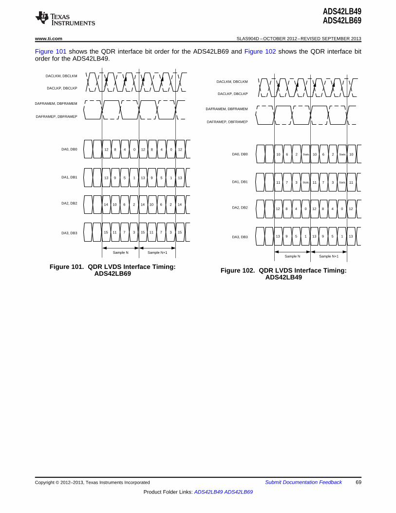
DA0, DB0
DACLKP, DBCLKP
DA1, DB1
DA2, DB2
DA3, DB3
DAFRAMEP, DBFRAMEP
DACLKM, DBCLKM
DAFRAMEM, DBFRAMEM
Sample N+1Sample N
13 9 5 1
12 8 4 0
11 7 3 Static
10 6 2 Static
13 9 5 1
12 8 4 0
11 7 3 Static
10 6 2 Static
13
12
11
10
DAFRAMEP, DBFRAMEP
DA0, DB0
DACLKP, DBCLKP
DA1, DB1
DA2, DB2
DA3, DB3
DACLKM, DBCLKM
DAFRAMEM, DBFRAMEM
Sample N+1Sample N
15 11 7 3
14 10 6 2
13 9 5 1
12 8 4 0
15 11 7 3
14 10 6 2
13 9 5 1
12 8 4 0
15
14
13
12
ADS42LB49ADS42LB69
www.ti.com SLAS904D –OCTOBER 2012–REVISED SEPTEMBER 2013
Figure 101 shows the QDR interface bit order for the ADS42LB69 and Figure 102 shows the QDR interface bitorder for the ADS42LB49.
Figure 101. QDR LVDS Interface Timing: Figure 102. QDR LVDS Interface Timing:ADS42LB69 ADS42LB49
Copyright © 2012–2013, Texas Instruments Incorporated Submit Documentation Feedback 69
Product Folder Links: ADS42LB49 ADS42LB69
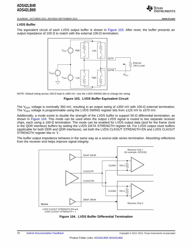
CLKOUTP
CLKOUTM
Device
LVDS CLKOUT STRENGTH EN andLVDS CLKOUT STRENGTH = 1
Receiver Chip 2
CLKIN2
DBnP, MDBn
100 W
Receiver Chip 1(for example, GC5330)
CLKIN1 100 W
DAnP, MDAn
VDIFF
VDIFF
VOCM
High
Low
Low
High
OUTP
OUTM
ROUT
External
100- LoadW
ADS42LB49ADS42LB69
SLAS904D –OCTOBER 2012–REVISED SEPTEMBER 2013 www.ti.com
LVDS BufferThe equivalent circuit of each LVDS output buffer is shown in Figure 103. After reset, the buffer presents anoutput impedance of 100 Ω to match with the external 100-Ω termination.
NOTE: Default swing across 100-Ω load is ±350 mV. Use the LVDS SWING bits to change the swing.
Figure 103. LVDS Buffer Equivalent Circuit
The VDIFF voltage is nominally 350 mV, resulting in an output swing of ±350 mV with 100-Ω external termination.The VDIFF voltage is programmable using the LVDS SWING register bits from ±125 mV to ±570 mV.
Additionally, a mode exists to double the strength of the LVDS buffer to support 50-Ω differential termination, asshown in Figure 104. This mode can be used when the output LVDS signal is routed to two separate receiverchips, each using a 100-Ω termination. The mode can be enabled for LVDS output data (and for the frame clockin the QDR interface) buffers by setting the LVDS DATA STRENGTH register bit. For LVDS output clock buffers(applicable for both DDR and QDR interfaces), set both the LVDS CLKOUT STRENGTH EN and LVDS CLKOUTSTRENGTH register bits to '1'.
The buffer output impedance behaves in the same way as a source-side series termination. Absorbing reflectionsfrom the receiver end helps improve signal integrity.
Figure 104. LVDS Buffer Differential Termination
70 Submit Documentation Feedback Copyright © 2012–2013, Texas Instruments Incorporated
Product Folder Links: ADS42LB49 ADS42LB69

ADS42LB49ADS42LB69
www.ti.com SLAS904D –OCTOBER 2012–REVISED SEPTEMBER 2013
Output Data FormatTwo output data formats are supported: twos complement and offset binary. The format can be selected usingthe DATA FORMAT serial interface register bit.
In the event of an input voltage overdrive, the digital outputs go to the appropriate full-scale level. For a positiveoverdrive, the output code is 3FFFh for the ADS42LB49 and ADS42LB69 in offset binary output format; theoutput code is 1FFFh for the ADS42LB49 and ADS42LB69 in twos complement output format. For a negativeinput overdrive, the output code is 0000h in offset binary output format and 2000h for the ADS42LB49 andADS42LB69 in twos complement output format.
Copyright © 2012–2013, Texas Instruments Incorporated Submit Documentation Feedback 71
Product Folder Links: ADS42LB49 ADS42LB69

ADS42LB49ADS42LB69
SLAS904D –OCTOBER 2012–REVISED SEPTEMBER 2013 www.ti.com
REVISION HISTORYNOTE: Page numbers for previous revisions may differ from page numbers in the current version.
Changes from Revision C (September 2013) to Revision D Page
• Changed device status to Production Data .......................................................................................................................... 1• Added pre-RTM changes throughout document ................................................................................................................... 1
Changes from Revision B (March 2013) to Revision C Page
• Added pre-RTM changes throughout document ................................................................................................................... 1
Changes from Revision A (November 2012) to Revision B Page
• Added pre-RTM changes throughout document ................................................................................................................... 1
Changes from Original (October 2012) to Revision A Page
• Added pre-RTM changes throughout document ................................................................................................................... 1
72 Submit Documentation Feedback Copyright © 2012–2013, Texas Instruments Incorporated
Product Folder Links: ADS42LB49 ADS42LB69

PACKAGE OPTION ADDENDUM
www.ti.com 18-Oct-2013
Addendum-Page 1
PACKAGING INFORMATION
Orderable Device Status(1)
Package Type PackageDrawing
Pins PackageQty
Eco Plan(2)
Lead/Ball Finish(6)
MSL Peak Temp(3)
Op Temp (°C) Device Marking(4/5)
Samples
ADS42LB49IRGC25 ACTIVE VQFN RGC 64 25 Green (RoHS& no Sb/Br)
CU NIPDAU | Call TI Level-3-260C-168 HR -40 to 85 AZ42LB49
ADS42LB49IRGCR ACTIVE VQFN RGC 64 2000 Green (RoHS& no Sb/Br)
CU NIPDAU | Call TI Level-3-260C-168 HR -40 to 85 AZ42LB49
ADS42LB49IRGCT ACTIVE VQFN RGC 64 250 Green (RoHS& no Sb/Br)
CU NIPDAU | Call TI Level-3-260C-168 HR -40 to 85 AZ42LB49
ADS42LB69IRGC25 ACTIVE VQFN RGC 64 25 Green (RoHS& no Sb/Br)
CU NIPDAU | Call TI Level-3-260C-168 HR -40 to 85 AZ42LB69
ADS42LB69IRGCR ACTIVE VQFN RGC 64 2000 Green (RoHS& no Sb/Br)
CU NIPDAU | Call TI Level-3-260C-168 HR -40 to 85 AZ42LB69
ADS42LB69IRGCT ACTIVE VQFN RGC 64 250 Green (RoHS& no Sb/Br)
CU NIPDAU | Call TI Level-3-260C-168 HR -40 to 85 AZ42LB69
(1) The marketing status values are defined as follows:ACTIVE: Product device recommended for new designs.LIFEBUY: TI has announced that the device will be discontinued, and a lifetime-buy period is in effect.NRND: Not recommended for new designs. Device is in production to support existing customers, but TI does not recommend using this part in a new design.PREVIEW: Device has been announced but is not in production. Samples may or may not be available.OBSOLETE: TI has discontinued the production of the device.
(2) Eco Plan - The planned eco-friendly classification: Pb-Free (RoHS), Pb-Free (RoHS Exempt), or Green (RoHS & no Sb/Br) - please check http://www.ti.com/productcontent for the latest availabilityinformation and additional product content details.TBD: The Pb-Free/Green conversion plan has not been defined.Pb-Free (RoHS): TI's terms "Lead-Free" or "Pb-Free" mean semiconductor products that are compatible with the current RoHS requirements for all 6 substances, including the requirement thatlead not exceed 0.1% by weight in homogeneous materials. Where designed to be soldered at high temperatures, TI Pb-Free products are suitable for use in specified lead-free processes.Pb-Free (RoHS Exempt): This component has a RoHS exemption for either 1) lead-based flip-chip solder bumps used between the die and package, or 2) lead-based die adhesive used betweenthe die and leadframe. The component is otherwise considered Pb-Free (RoHS compatible) as defined above.Green (RoHS & no Sb/Br): TI defines "Green" to mean Pb-Free (RoHS compatible), and free of Bromine (Br) and Antimony (Sb) based flame retardants (Br or Sb do not exceed 0.1% by weightin homogeneous material)
(3) MSL, Peak Temp. - The Moisture Sensitivity Level rating according to the JEDEC industry standard classifications, and peak solder temperature.
(4) There may be additional marking, which relates to the logo, the lot trace code information, or the environmental category on the device.
(5) Multiple Device Markings will be inside parentheses. Only one Device Marking contained in parentheses and separated by a "~" will appear on a device. If a line is indented then it is a continuationof the previous line and the two combined represent the entire Device Marking for that device.

PACKAGE OPTION ADDENDUM
www.ti.com 18-Oct-2013
Addendum-Page 2
(6) Lead/Ball Finish - Orderable Devices may have multiple material finish options. Finish options are separated by a vertical ruled line. Lead/Ball Finish values may wrap to two lines if the finishvalue exceeds the maximum column width.
Important Information and Disclaimer:The information provided on this page represents TI's knowledge and belief as of the date that it is provided. TI bases its knowledge and belief on informationprovided by third parties, and makes no representation or warranty as to the accuracy of such information. Efforts are underway to better integrate information from third parties. TI has taken andcontinues to take reasonable steps to provide representative and accurate information but may not have conducted destructive testing or chemical analysis on incoming materials and chemicals.TI and TI suppliers consider certain information to be proprietary, and thus CAS numbers and other limited information may not be available for release.
In no event shall TI's liability arising out of such information exceed the total purchase price of the TI part(s) at issue in this document sold by TI to Customer on an annual basis.

TAPE AND REEL INFORMATION
*All dimensions are nominal
Device PackageType
PackageDrawing
Pins SPQ ReelDiameter
(mm)
ReelWidth
W1 (mm)
A0(mm)
B0(mm)
K0(mm)
P1(mm)
W(mm)
Pin1Quadrant
ADS42LB49IRGCR VQFN RGC 64 2000 330.0 16.4 9.3 9.3 1.5 12.0 16.0 Q2
ADS42LB49IRGCT VQFN RGC 64 250 180.0 16.4 9.3 9.3 1.5 12.0 16.0 Q2
ADS42LB69IRGCR VQFN RGC 64 2000 330.0 16.4 9.3 9.3 1.5 12.0 16.0 Q2
ADS42LB69IRGCT VQFN RGC 64 250 180.0 16.4 9.3 9.3 1.5 12.0 16.0 Q2
PACKAGE MATERIALS INFORMATION
www.ti.com 21-Mar-2014
Pack Materials-Page 1

*All dimensions are nominal
Device Package Type Package Drawing Pins SPQ Length (mm) Width (mm) Height (mm)
ADS42LB49IRGCR VQFN RGC 64 2000 336.6 336.6 28.6
ADS42LB49IRGCT VQFN RGC 64 250 213.0 191.0 55.0
ADS42LB69IRGCR VQFN RGC 64 2000 336.6 336.6 28.6
ADS42LB69IRGCT VQFN RGC 64 250 213.0 191.0 55.0
PACKAGE MATERIALS INFORMATION
www.ti.com 21-Mar-2014
Pack Materials-Page 2


IMPORTANT NOTICETexas Instruments Incorporated and its subsidiaries (TI) reserve the right to make corrections, enhancements, improvements and otherchanges to its semiconductor products and services per JESD46, latest issue, and to discontinue any product or service per JESD48, latestissue. Buyers should obtain the latest relevant information before placing orders and should verify that such information is current andcomplete. All semiconductor products (also referred to herein as “components”) are sold subject to TI’s terms and conditions of salesupplied at the time of order acknowledgment.TI warrants performance of its components to the specifications applicable at the time of sale, in accordance with the warranty in TI’s termsand conditions of sale of semiconductor products. Testing and other quality control techniques are used to the extent TI deems necessaryto support this warranty. Except where mandated by applicable law, testing of all parameters of each component is not necessarilyperformed.TI assumes no liability for applications assistance or the design of Buyers’ products. Buyers are responsible for their products andapplications using TI components. To minimize the risks associated with Buyers’ products and applications, Buyers should provideadequate design and operating safeguards.TI does not warrant or represent that any license, either express or implied, is granted under any patent right, copyright, mask work right, orother intellectual property right relating to any combination, machine, or process in which TI components or services are used. Informationpublished by TI regarding third-party products or services does not constitute a license to use such products or services or a warranty orendorsement thereof. Use of such information may require a license from a third party under the patents or other intellectual property of thethird party, or a license from TI under the patents or other intellectual property of TI.Reproduction of significant portions of TI information in TI data books or data sheets is permissible only if reproduction is without alterationand is accompanied by all associated warranties, conditions, limitations, and notices. TI is not responsible or liable for such altereddocumentation. Information of third parties may be subject to additional restrictions.Resale of TI components or services with statements different from or beyond the parameters stated by TI for that component or servicevoids all express and any implied warranties for the associated TI component or service and is an unfair and deceptive business practice.TI is not responsible or liable for any such statements.Buyer acknowledges and agrees that it is solely responsible for compliance with all legal, regulatory and safety-related requirementsconcerning its products, and any use of TI components in its applications, notwithstanding any applications-related information or supportthat may be provided by TI. Buyer represents and agrees that it has all the necessary expertise to create and implement safeguards whichanticipate dangerous consequences of failures, monitor failures and their consequences, lessen the likelihood of failures that might causeharm and take appropriate remedial actions. Buyer will fully indemnify TI and its representatives against any damages arising out of the useof any TI components in safety-critical applications.In some cases, TI components may be promoted specifically to facilitate safety-related applications. With such components, TI’s goal is tohelp enable customers to design and create their own end-product solutions that meet applicable functional safety standards andrequirements. Nonetheless, such components are subject to these terms.No TI components are authorized for use in FDA Class III (or similar life-critical medical equipment) unless authorized officers of the partieshave executed a special agreement specifically governing such use.Only those TI components which TI has specifically designated as military grade or “enhanced plastic” are designed and intended for use inmilitary/aerospace applications or environments. Buyer acknowledges and agrees that any military or aerospace use of TI componentswhich have not been so designated is solely at the Buyer's risk, and that Buyer is solely responsible for compliance with all legal andregulatory requirements in connection with such use.TI has specifically designated certain components as meeting ISO/TS16949 requirements, mainly for automotive use. In any case of use ofnon-designated products, TI will not be responsible for any failure to meet ISO/TS16949.Products ApplicationsAudio www.ti.com/audio Automotive and Transportation www.ti.com/automotiveAmplifiers amplifier.ti.com Communications and Telecom www.ti.com/communicationsData Converters dataconverter.ti.com Computers and Peripherals www.ti.com/computersDLP® Products www.dlp.com Consumer Electronics www.ti.com/consumer-appsDSP dsp.ti.com Energy and Lighting www.ti.com/energyClocks and Timers www.ti.com/clocks Industrial www.ti.com/industrialInterface interface.ti.com Medical www.ti.com/medicalLogic logic.ti.com Security www.ti.com/securityPower Mgmt power.ti.com Space, Avionics and Defense www.ti.com/space-avionics-defenseMicrocontrollers microcontroller.ti.com Video and Imaging www.ti.com/videoRFID www.ti-rfid.comOMAP Applications Processors www.ti.com/omap TI E2E Community e2e.ti.comWireless Connectivity www.ti.com/wirelessconnectivity
Mailing Address: Texas Instruments, Post Office Box 655303, Dallas, Texas 75265Copyright © 2014, Texas Instruments Incorporated