ece 545 lecture 7 fpga design...
TRANSCRIPT

George Mason University
FPGA Design Flow
ECE 545 Lecture 7
2
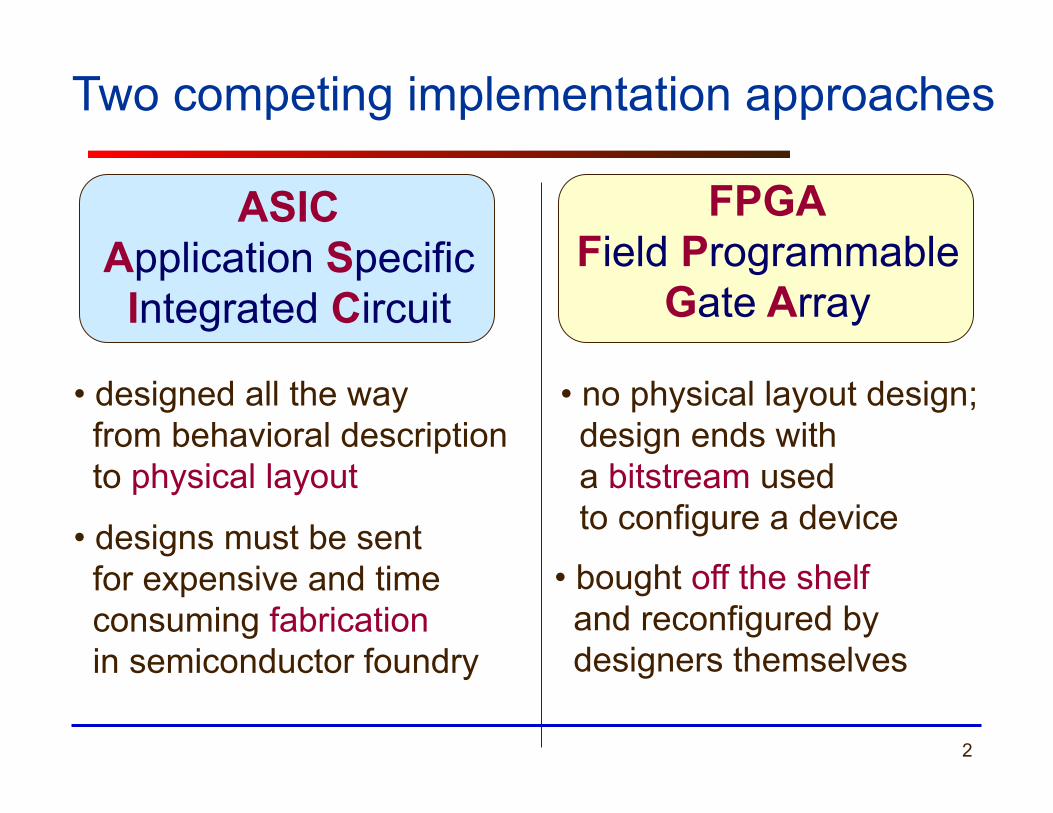
• designs must be sent for expensive and time consuming fabrication in semiconductor foundry
• bought off the shelf and reconfigured by designers themselves
Two competing implementation approaches
ASIC Application Specific
Integrated Circuit
FPGA Field Programmable
Gate Array
• designed all the way from behavioral description to physical layout
• no physical layout design; design ends with a bitstream used to configure a device

3
Which Way to Go?
Off-the-shelf
Low development cost
Short time to market
Reconfigurability
High performance
ASICs FPGAs
Low power
Low cost in high volumes

4
Block R
AM
s
Block R
AM
s
Basic Logic Blocks
I/O Blocks
What is an FPGA?
Block RAMs

5
Modern FPGA RAM blocks
Multipliers
Logic blocks
Graphics based on The Design Warrior’s Guide to FPGAs Devices, Tools, and Flows. ISBN 0750676043
Copyright © 2004 Mentor Graphics Corp. (www.mentor.com)
Multipliers/DSP units
RAM blocks
Logic resources
(#Logic resources, #Multipliers/DSP units, #RAM_blocks)

Technology Low-‐cost High-‐performance
220 nm Virtex 180 nm Spartan II,
Spartan IIE 120/150 nm Virtex II,
Virtex II Pro 90 nm Spartan 3 Virtex 4 65 nm Virtex 5 45 nm Spartan 6 40 nm Virtex 6 28 nm Ar?x 7 Virtex 7
Xilinx FPGA Families

Altera FPGA Families Technology Low-‐cost Mid-‐range High-‐
performance
130 nm Cyclone Stra@x
90 nm Cyclone II Stra?x II
65 nm Cyclone III Arria I Stra?x III
40 nm Cyclone IV Arria II Stra?x IV
28 nm Cyclone V Arria V Stra?x V

George Mason University
Spartan-3 Family Attributes

9
Spartan-3 FPGA Family Members

10
FPGA Nomenclature
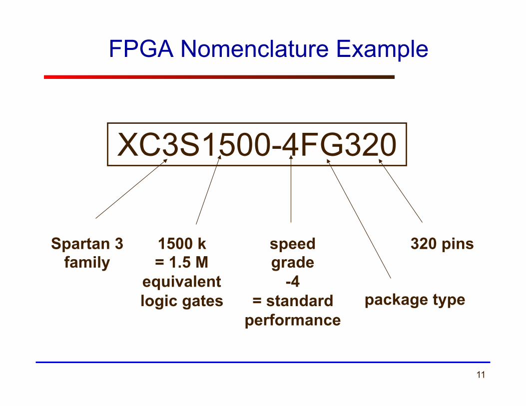
11
FPGA Nomenclature Example
XC3S1500-4FG320
Spartan 3 family
1500 k = 1.5 M
equivalent logic gates
speed grade
-4 = standard
performance
320 pins
package type

George Mason University
FPGA Design Flow

FPGA Design process (1) Design and implement a simple unit permitting to speed up encryption with RC5-similar cipher with fixed key set on 8031 microcontroller. Unlike in the experiment 5, this time your unit has to be able to perform an encryption algorithm by itself, executing 32 rounds…..
Library IEEE; use ieee.std_logic_1164.all; use ieee.std_logic_unsigned.all; entity RC5_core is port( clock, reset, encr_decr: in std_logic; data_input: in std_logic_vector(31 downto 0); data_output: out std_logic_vector(31 downto 0); out_full: in std_logic; key_input: in std_logic_vector(31 downto 0); key_read: out std_logic; ); end AES_core;
Specification / Pseudocode
VHDL description (Your Source Files) Functional simulation
Post-synthesis simulation Synthesis
On-paper hardware design (Block diagram & ASM chart)

FPGA Design process (2)
Implementation
Configuration
Timing simulation
On chip testing

15
Tools used in FPGA Design Flow
Xilinx XST
Design
Synthesis
Implementation
Xilinx ISE
VHDL code
Netlist
Bitstream
Synplify Premier
Functionally verified
VHDL code

George Mason University
Synthesis

17
Synthesis Tools
… and others
Synplify Premier Xilinx XST

18
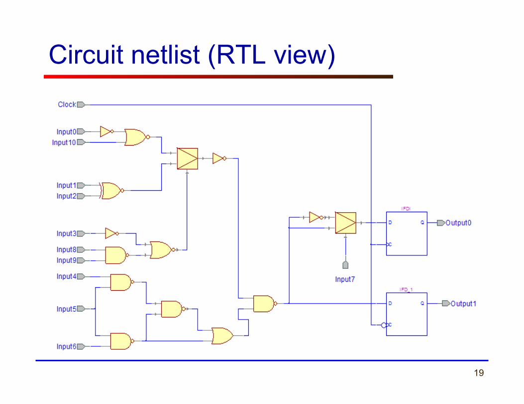
architecture MLU_DATAFLOW of MLU is
signal A1:STD_LOGIC; signal B1:STD_LOGIC; signal Y1:STD_LOGIC; signal MUX_0, MUX_1, MUX_2, MUX_3: STD_LOGIC; begin
A1<=A when (NEG_A='0') else not A; B1<=B when (NEG_B='0') else not B; Y<=Y1 when (NEG_Y='0') else not Y1; MUX_0<=A1 and B1; MUX_1<=A1 or B1; MUX_2<=A1 xor B1; MUX_3<=A1 xnor B1; with (L1 & L0) select Y1<=MUX_0 when "00", MUX_1 when "01", MUX_2 when "10", MUX_3 when others;
end MLU_DATAFLOW;
VHDL description Circuit netlist
Logic Synthesis
19
Circuit netlist (RTL view)

20
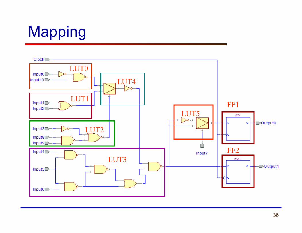
Mapping
LUT2
LUT3
LUT4
LUT5
LUT1 FF1
FF2
LUT0

21
Xilinx XST Inputs/Outputs

22
Xilinx XST Inputs
• RTL VHDL and/or Verilog files • Core files
These files can be in either NGC or EDIF format. XST does not modify cores. It uses them to inform area and timing optimization surrounding the cores.
• Constraints – XCF Xilinx constraints file in which you can specify synthesis, timing, and specific implementation constraints that can be propagated to the NGC file.

23
Xilinx XST Outputs • NGC
Netlist file with constraint information • NGR
This is a schematic representation of the pre-optimized design shown at the Register Transfer Level (RTL). This representation is in terms of generic symbols, such as adders, multipliers, counters, AND gates, and OR gates, and is generated after the HDL synthesis phase of the synthesis process.
• LOG This report contains the results from the synthesis run, including area and timing estimation.
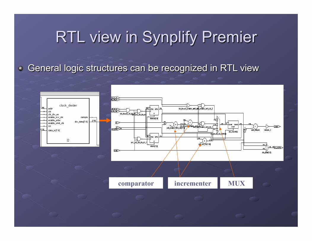
RTL view in Synplify Premier
incrementer comparator
" General logic structures can be recognized in RTL view
MUX

Crossprobing between RTL view and code " Each port, net or block can be chosen by mouse click from the
browser or directly from the RTL View
" By double-clicking on the element its source code can be seen:
" Reverse crossprobing is also possible: if section of code is marked, appropriate element of RTL View is marked too:

Technology View in Synplify Pro
" Technology view is a mapped RTL view. It can be seen by pressing button or by double-click on “.srm” file
" As in case of “RTL View”, buttons can be used here
" Two additional buttons are enabled: - show critical path - open timing analyst
Technology view is presented using device primitives Ports, nets and
blocks browser
Pay attention: technology view is usually large and presented on number of sheets
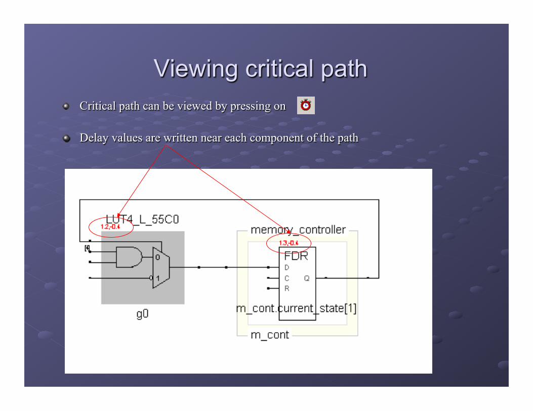
Viewing critical path " Critical path can be viewed by pressing on
" Delay values are written near each component of the path

Timing Analyst " Timing analyst opened by pressing on " Timing analyst gives a possibility to analyze different paths in the design " Timing analyst can be opened only from Technology View
George Mason University
Implementation
30
Implementation
• After synthesis the entire implementation process is performed by FPGA vendor tools

31
Implementation

32
Translation
Translation
UCF
NGD
EDIF NCF
Native Generic Database file
Constraint Editor or Text Editor
User Constraint File
Native Constraint
File
Electronic Design Interchange Format
Circuit netlist Timing Constraints
Synthesis

33
Pin Assignment
LAB5
CLOCK CONTROL(0)
CONTROL(2) CONTROL(1)
RESET
SEGMENTS(0) SEGMENTS(1) SEGMENTS(2) SEGMENTS(3) SEGMENTS(4) SEGMENTS(5) SEGMENTS(6)
H3
K2 G5
K3 H1 K4
G4
H5
H6
H2
P10
B10 FPGA

34

35
Example of an UCF File
NET "CLOCK" LOC = "P10";
NET "reset" LOC = "B10"; NET "S_SEG0<6>" LOC = "H1";
NET "S_SEG0<5>” LOC = "G4";
NET "S_SEG0<4>” LOC = "G5";
NET "S_SEG0<3>” LOC = "H5";
NET "S_SEG0<2>” LOC = "H6"; NET "S_SEG0<1>” LOC = "H3";
NET "S_SEG0<0>” LOC = "H2";
ECE 448 – FPGA and ASIC Design with VHDL
36
Mapping
LUT2
LUT3
LUT4
LUT5
LUT1 FF1
FF2
LUT0
37
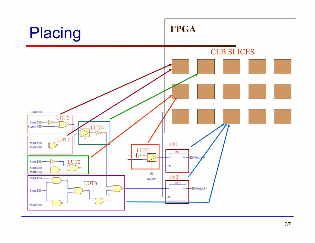
Placing CLB SLICES
FPGA

38
Routing Programmable Connections
FPGA
39
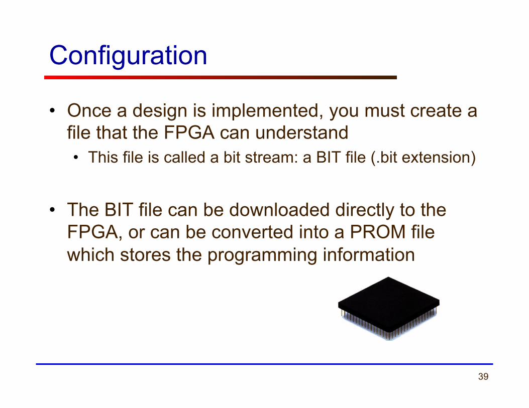
Configuration
• Once a design is implemented, you must create a file that the FPGA can understand • This file is called a bit stream: a BIT file (.bit extension)
• The BIT file can be downloaded directly to the FPGA, or can be converted into a PROM file which stores the programming information

Two main stages of the FPGA Design Flow
Synthesis
Technology independent
Technology dependent
Implementation
RTL Synthesis Map Place & Route Configure
- Code analysis - Derivation of main logic constructions - Technology independent optimization - Creation of “RTL View”
- Mapping of extracted logic structures to device primitives - Technology dependent optimization - Application of “synthesis constraints” - Netlist generation - Creation of “Technology View”
- Placement of generated netlist onto the device - Choosing best interconnect structure for the placed design - Application of “physical constraints”
- Bitstream generation - Burning device

41 ECE 448 – FPGA and ASIC Design with VHDL
Report files

42
Map report header
Xilinx Mapping Report File for Design 'Lab3Demo' Design Information ------------------ Command Line : c:\Xilinx\bin\nt\map.exe -p 3S1500FG320-4 -o map.ncd -pr b -k 4 -cm area -c 100 Lab3Demo.ngd Lab3Demo.pcf Target Device : xc3s1500 Target Package : fg320 Target Speed : -4 Mapper Version : spartan3 -- $Revision: 1.34 $
43
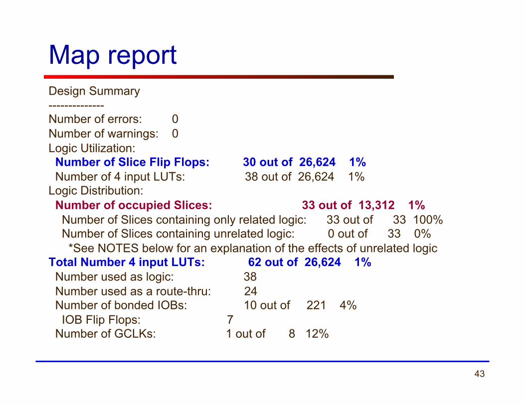
Map report Design Summary -------------- Number of errors: 0 Number of warnings: 0 Logic Utilization: Number of Slice Flip Flops: 30 out of 26,624 1% Number of 4 input LUTs: 38 out of 26,624 1% Logic Distribution: Number of occupied Slices: 33 out of 13,312 1% Number of Slices containing only related logic: 33 out of 33 100% Number of Slices containing unrelated logic: 0 out of 33 0% *See NOTES below for an explanation of the effects of unrelated logic Total Number 4 input LUTs: 62 out of 26,624 1% Number used as logic: 38 Number used as a route-thru: 24 Number of bonded IOBs: 10 out of 221 4% IOB Flip Flops: 7 Number of GCLKs: 1 out of 8 12%
44
Related and Unrelated Logic Related logic is defined as being logic that shares connectivity – e.g. two LUTs are "related" if they share common inputs. When assembling slices, Map gives priority to combine logic that is related. Doing so results in the best timing performance. Unrelated logic shares no connectivity. Map will only begin packing unrelated logic into a slice once 99% of the slices are occupied through related logic packing. Note that once logic distribution reaches the 99% level through related logic packing, this does not mean the device is completely utilized. Unrelated logic packing will then begin, continuing until all usable LUTs and FFs are occupied. Depending on your timing budget, increased levels of unrelated logic packing may adversely affect the overall timing performance of your design.

45
Place & route report
Asterisk (*) preceding a constraint indicates it was not met. This may be due to a setup or hold violation. ------------------------------------------------------------------------------------------------------ Constraint | Requested | Actual | Logic | Absolute |Number of | | | Levels | Slack |errors ------------------------------------------------------------------------------------------------------ * TS_CLOCK = PERIOD TIMEGRP "CLOCK" 5 ns | 5.000ns | 5.140ns | 4 | -0.140ns | 5 HIGH 50% | | | | | ------------------------------------------------------------------------------------------------------ TS_gen1Hz_Clock1Hz = PERIOD TIMEGRP "gen1 | 5.000ns | 4.137ns | 2 | 0.863ns | 0 "gen1Hz_Clock1Hz" 5 ns HIGH 50% | | | | | ------------------------------------------------------------------------------------------------------

46
Post layout timing report Clock to Setup on destination clock CLOCK ---------------+---------+---------+---------+---------+ | Src:Rise| Src:Fall| Src:Rise| Src:Fall| Source Clock |Dest:Rise|Dest:Rise|Dest:Fall|Dest:Fall| ---------------+---------+---------+---------+---------+ CLOCK | 5.140| | | | ---------------+---------+---------+---------+---------+ Timing summary: --------------- Timing errors: 9 Score: 543 Constraints cover 574 paths, 0 nets, and 187 connections Design statistics: Minimum period: 5.140ns (Maximum frequency: 194.553MHz)