ece 551 digital design and synthesis spring 2006 course introduction review
Post on 21-Dec-2015
220 views
TRANSCRIPT
ECE 551Digital Design And
Synthesis
Spring 2006
Course IntroductionReview
2
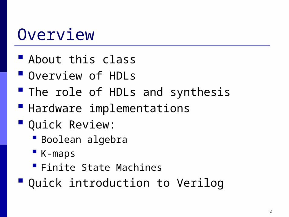
Overview About this class Overview of HDLs The role of HDLs and synthesis Hardware implementations Quick Review:
Boolean algebra K-maps Finite State Machines
Quick introduction to Verilog

3
Course Purpose Provide knowledge and experience in:
Contemporary logic design using an HDL (Verilog)
HDL simulation Synthesis of structural and behavioral designs Analysis of design tradeoffs Optimizing hardware designs Design tools commonly used in industry
Teach you to be able to “think hardware”

4
What You Should Already Know Principles of basic digital logic design (ECE
352) Boolean algebra Gate-level design K-Map minimization Sequential logic design Finite State Machines
How to log in to CAE machines and use a shell

5
Course Information Class times
Lecture: 1:00-2:15 Tuesday & Thursday, 2540 EH
Discussion: 4:30-5:30 Thursday, 1209 EH No discussion section this week
Instructor office hours Prof. Mike Schulte [email protected],
4619 EH Office Hours: Tuesday & Thursday, 2:30-3:30

6
Course Website eCOW
http://courses.engr.wisc.edu/ecow/get/ece/551/2schulte/ Password: fall06_551 (for portions of website)
Resource Syllabus Course updates Tutorials Lecture notes, supplemental readings Homework assignments Project information
CHECK IT OFTEN

7
Course Materials Lectures Text
M. D. Cilleti, Advanced Digital Design with the Verilog HDL, Prentice Hall, 2003.
Standards IEEE Std.1364-2001, IEEE Standard Verilog
Hardware Description Language, IEEE, Inc., 2001.
IEEE Std 1364.1-2002, IEEE Standard for Verilog Register Transfer Level Synthesis, IEEE, Inc., 2002
Synopsys on-line documentation
8
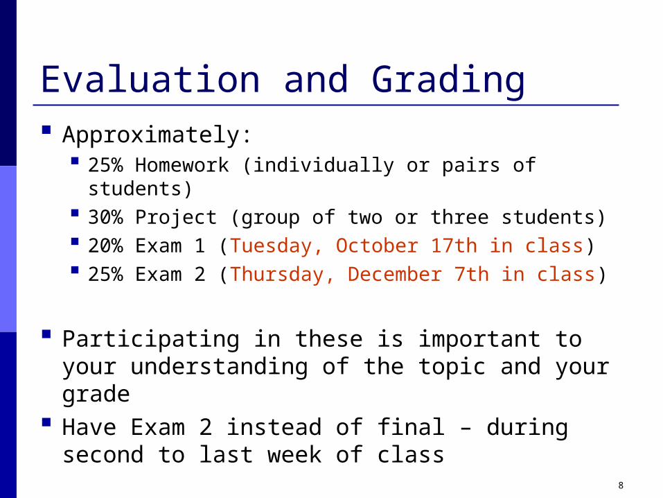
Evaluation and Grading Approximately:
25% Homework (individually or pairs of students)
30% Project (group of two or three students) 20% Exam 1 (Tuesday, October 17th in class) 25% Exam 2 (Thursday, December 7th in class)
Participating in these is important to your understanding of the topic and your grade
Have Exam 2 instead of final – during second to last week of class

9
Homeworks Assignments will either be individual or in
pairs Read the assignment to see! Start looking for homework & project partners
Homework due at beginning of class 10% penalty for each late period of 24 hours Not accepted >72 hours after deadline Your responsibility to get it to me
Can leave in my mailbox with a timestamp of when it was turned in

10
Class Project Work in groups of 2 or 3 students Design, model, simulate, and synthesize
real-world hardware circuit(s) This semester
Fast Fourier Transform (FFT) processor Computations use floating-point arithmetic Pipelined for high performance More details available soon

11
Course Tools Industry-standard design tools:
Modelsim HDL Simulation Tools (Mentor) Design Vision Synthesis Tools (Synopsys) LSI Logic Gflx 0.11 Micron CMOS Standard Cell
Technology Library
Tutorials will be available for both tools Modelsim tutorial next week (can start now) Design Vision tutorial a few weeks later Will be required as part of homework Can do on own time (within deadline) TA will set a time for a “help session”
12
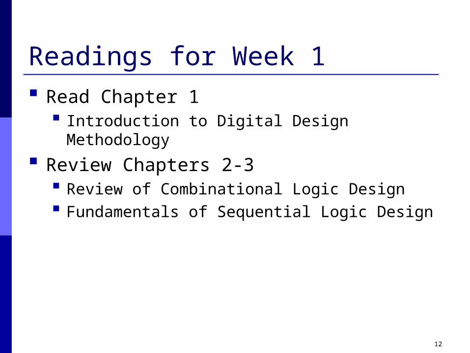
Readings for Week 1 Read Chapter 1
Introduction to Digital Design Methodology
Review Chapters 2-3 Review of Combinational Logic Design Fundamentals of Sequential Logic Design
13
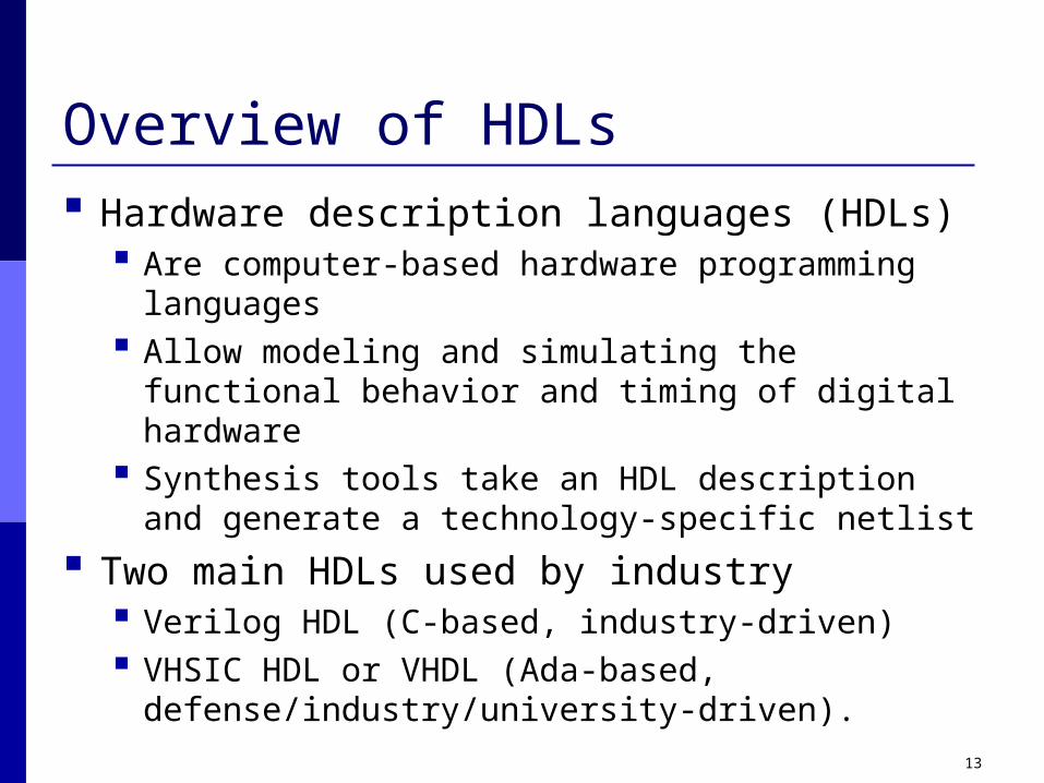
Overview of HDLs Hardware description languages (HDLs)
Are computer-based hardware programming languages
Allow modeling and simulating the functional behavior and timing of digital hardware
Synthesis tools take an HDL description and generate a technology-specific netlist
Two main HDLs used by industry Verilog HDL (C-based, industry-driven) VHSIC HDL or VHDL (Ada-based,
defense/industry/university-driven).
14
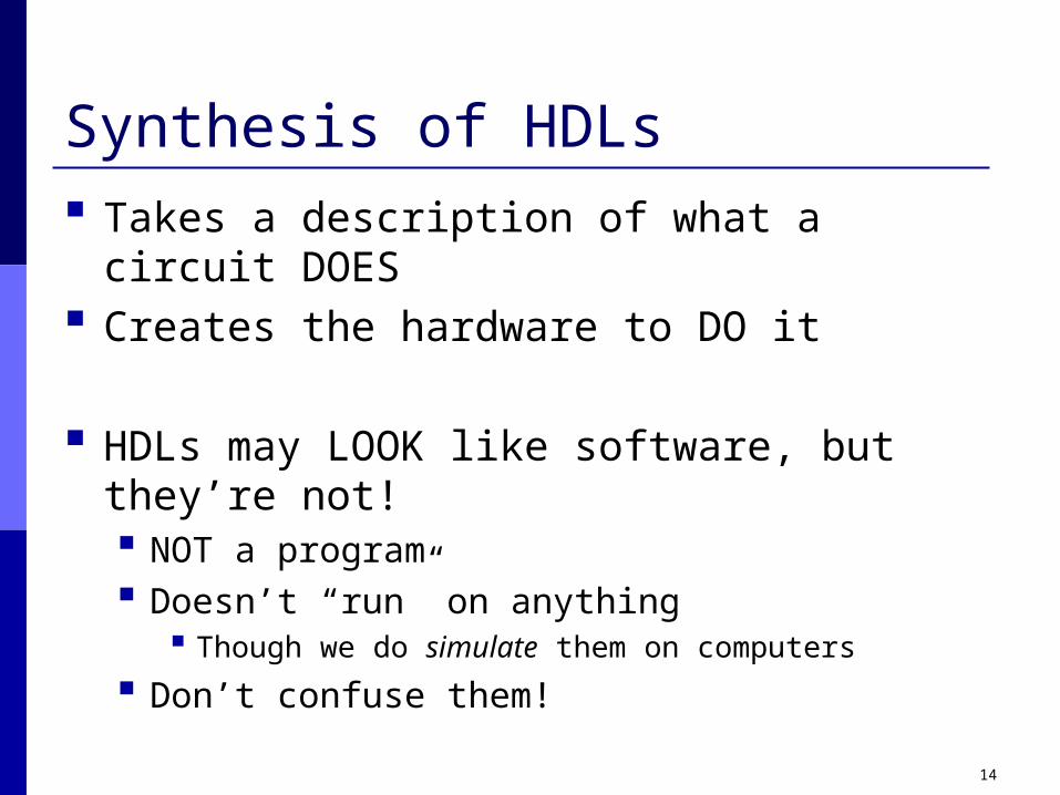
Synthesis of HDLs Takes a description of what a circuit DOES Creates the hardware to DO it
HDLs may LOOK like software, but they’re not! NOT a program Doesn’t “run” on anything
Though we do simulate them on computers
Don’t confuse them!
15
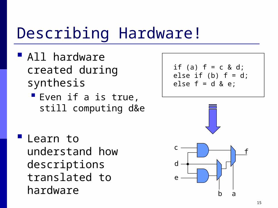
Describing Hardware! All hardware created
during synthesis Even if a is true, still
computing d&e
Learn to understand how descriptions translated to hardware
if (a) f = c & d; else if (b) f = d; else f = d & e;
f
ab
c
d
e

16
Why Use an HDL? More and more transistors can fit on a chip
Allows larger designs! Work at transistor/gate level for large designs:
hard Many designs need to go to production quickly
Abstract large hardware designs! Describe what you need the hardware to do Tools then design the hardware for you
BIG CAVEAT Good descriptions => Good hardware Bad descriptions => BAD hardware!
17
Why Use an HDL? Simplified & faster design process Explore larger solution space
Smaller, faster, lower power Throughput vs. latency Examine more design tradeoffs
Lessen the time spent debugging the design Design errors still possible, but in fewer places Generally easier to find and fix
Can reuse design to target different technologies Don’t manually change all transistors for rule
change

18
Other Important HDL Features Are highly portable (text) Are self-documenting (when commented
well) Describe multiple levels of abstraction Represent parallelism Provides many descriptive styles
Structural Register Transfer Level (RTL) Behavioral
Serve as input for synthesis tools

19
Hardware Implementations HDLs can be compiled to semi-custom and
programmable hardware implementations
Standard Cell
Gate Array
FPGA PLDManual
VLSI
Full Custom
Semi-Custom
Programmable
less work, faster time to market
implementation efficiency

20
Hardware Building Blocks Transistors are switches
Use multiple transistors to make a gate
Use multiple gates to make a circuit
AAAA
A
B C
21
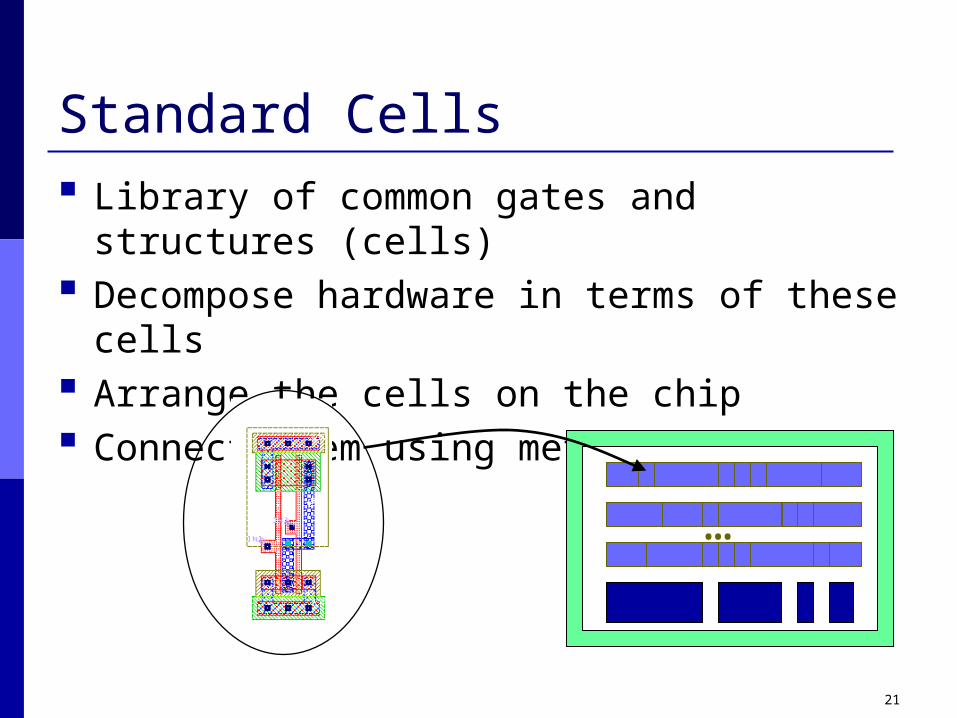
Standard Cells Library of common gates and structures
(cells) Decompose hardware in terms of these
cells Arrange the cells on the chip Connect them using metal wiring
…
22
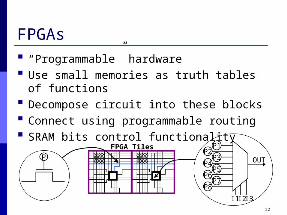
FPGAs “Programmable” hardware Use small memories as truth tables of
functions Decompose circuit into these blocks Connect using programmable routing SRAM bits control functionality
P
P1P2P3
P4P5
P6P7
P8
I1 I3I2
OUT
FPGA Tiles

23
Review: Boolean Algebra and K-maps I just said we’re abstracting hardware
design… Why do you need to understand hardware?
In truth, good hardware design requires ability to analyze a problem to find simplifications Which may involve boolean equations, K-maps
Why bother simplifying? Easier to design/debug, speed up synthesis Can have smaller/faster resulting hardware Synthesis tool only knows what you tell it

24
Example: Boolean Algebra
F = (A + B + C)(A + BC)

25
Example: K-Mapw x y z f
0 0 0 0 00 0 0 1 10 0 1 0 00 0 1 1 10 1 0 0 10 1 0 1 10 1 1 0 10 1 1 1 11 0 0 0 01 0 0 1 01 0 1 0 01 0 1 1 01 1 0 0 11 1 0 1 01 1 1 0 11 1 1 1 0

26
FSM Review Combinational and sequential logic Often used to generate control signals Reacts to inputs (including clock signal) Can perform multi-cycle operations
Examples of FSMs Counter Vending machine Traffic light controller Phone dialing

27
Mealy/Moore FSMs
Next State Logic
FF
State Register
InputsOutputs
OutputLogic
Mealy
Next StateCurrent State

28
FSMs Moore
Output depends only on current state Outputs are synchronous
Mealy Output depends on current state and inputs Outputs can be asynchronous
Change with changes on the inputs
Outputs can be synchronous Register the outputs Outputs delayed by one cycle
29
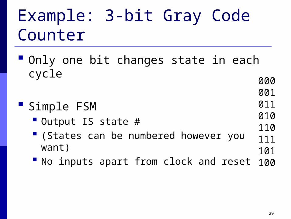
Example: 3-bit Gray Code Counter Only one bit changes state in each cycle
Simple FSM Output IS state # (States can be numbered however you want) No inputs apart from clock and reset
000001011010110111101100

30
Verilog In this class, we will use the Verilog HDL
Used in academia and industry
VHDL is another common HDL Also used by both academia and industry
Many principles we will discuss apply to any HDL
Once you can “think hardware”, you should be able to use any HDL fairly quickly
31
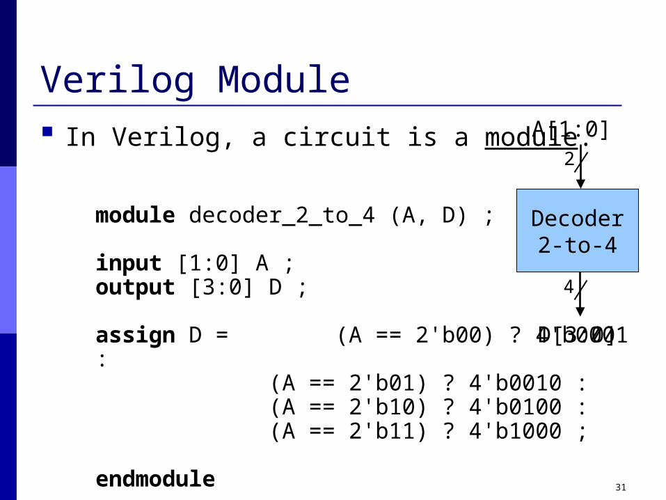
Verilog Module In Verilog, a circuit is a module.
module decoder_2_to_4 (A, D) ;
input [1:0] A ;output [3:0] D ;
assign D = (A == 2'b00) ? 4'b0001 : (A == 2'b01) ? 4'b0010 :
(A == 2'b10) ? 4'b0100 : (A == 2'b11) ? 4'b1000 ;
endmodule
Decoder2-to-4
A[1:0]
D[3:0]
2
4

32
Verilog Module
module decoder_2_to_4 (A, D) ;
input [1:0] A ;output [3:0] D ;
assign D = (A == 2'b00) ? 4'b0001 : (A == 2'b01) ? 4'b0010 :
(A == 2'b10) ? 4'b0100 : (A == 2'b11) ? 4'b1000 ;
endmodule
Decoder2-to-4
A[1:0]
D[3:0]
2
4
ports names of module
module name
port types
port sizes
module contents
keywords underlined

33
Declaring A Module Can’t use keywords as module/port/signal
names Choose a descriptive module name
Indicate the ports (connectivity)
Declare the signals connected to the ports Choose descriptive signal names
Declare any internal signals
Write the internals of the module (functionality)
34
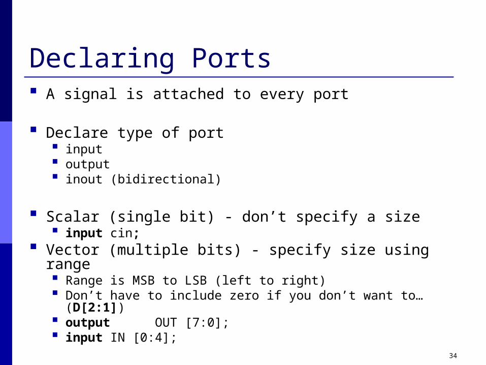
Declaring Ports A signal is attached to every port
Declare type of port input output inout (bidirectional)
Scalar (single bit) - don’t specify a size input cin;
Vector (multiple bits) - specify size using range Range is MSB to LSB (left to right) Don’t have to include zero if you don’t want to…
(D[2:1]) output OUT [7:0]; input IN [0:4];

35
Module Styles Modules can be specified different ways
Structural – connect primitives and modules RTL – use continuous assignments Behavioral – use initial and always blocks
A single module can use more than one method!
What are the differences?
36
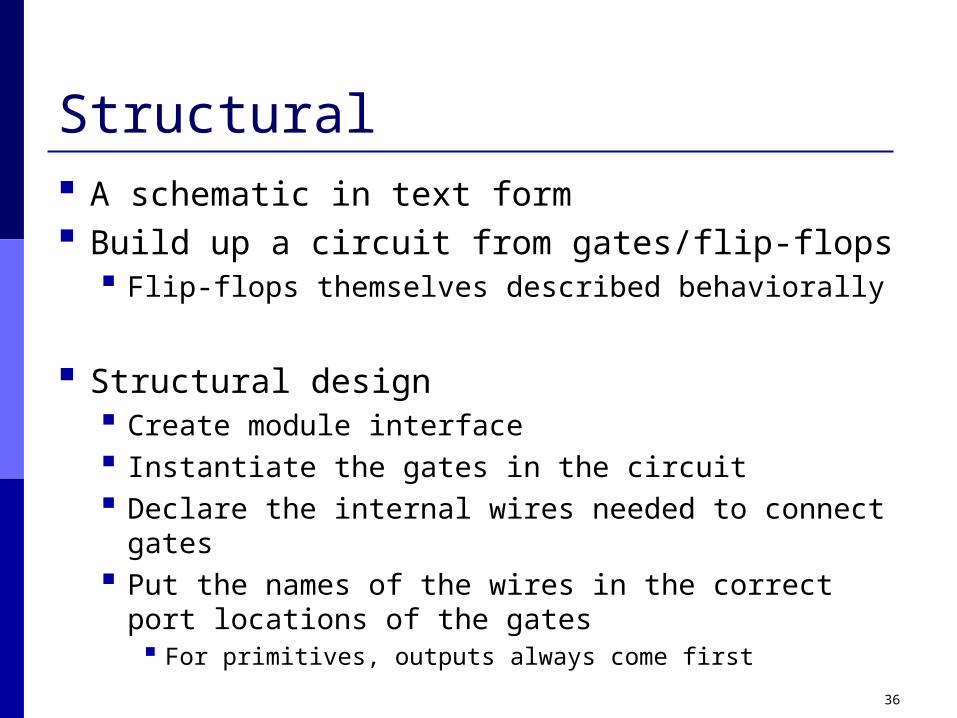
Structural A schematic in text form Build up a circuit from gates/flip-flops
Flip-flops themselves described behaviorally
Structural design Create module interface Instantiate the gates in the circuit Declare the internal wires needed to connect
gates Put the names of the wires in the correct port
locations of the gates For primitives, outputs always come first
37
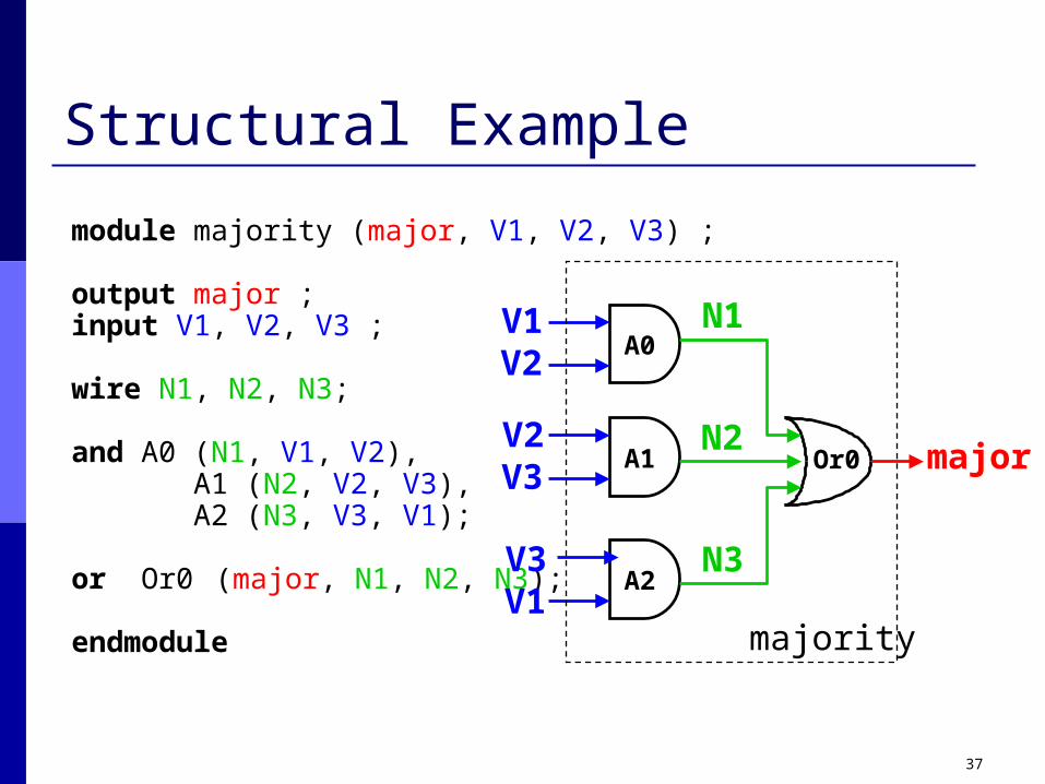
Structural Example
module majority (major, V1, V2, V3) ;
output major ;input V1, V2, V3 ;
wire N1, N2, N3;
and A0 (N1, V1, V2), A1 (N2, V2, V3), A2 (N3, V3, V1);
or Or0 (major, N1, N2, N3);
endmodule
V1V2
V2V3
V3V1
major
N1
N2
N3
A0
A1
A2
Or0
majority
38
RTL Example
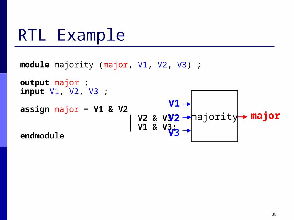
module majority (major, V1, V2, V3) ;
output major ;input V1, V2, V3 ;
assign major = V1 & V2 | V2 & V3 | V1 & V3;endmodule
V1
V2
V3
majormajority

39
Behavioral Example
module majority (major, V1, V2, V3) ;
output reg major ;input V1, V2, V3 ;
always @(V1, V2, V3) beginif (V1 && V2 || V2 && V3
|| V1 && V3) major = 1; else major = 0;end
endmodule
V1
V2
V3
majormajority
40
Things to do Read Chapter 1
Introduction to Digital Design Methodology
Review Chapters 2-3 Review of Combinational Logic Design Fundamentals of Sequential Logic Design
Look over course syllabus Start ModelSim tutorial