ece 590: digital design using hdl
TRANSCRIPT
ECE 590: DIGITAL DESIGN USING HDL
Final Project
A TRIANGULAR SORTER USING
MEMRISTOR ARCHITECTURE
Under the Leadership and Guidance of
Dr. Marek A Perkowski – Director of Intelligent Robotics
By,
Sai Kiran Kadam
PSU ID 914459405
ECE Graduate Student.

Contents:
1. Abstract
2. Introduction
3. Triangular Sorter
4. Memristor
4.1. Structure and Characteristics
4.2 Advantages and Dis-advantages
5. Imply Gate
5.1 Imply Logic Implementation
5.2 Imply Logic Diagram
6. Max/Min Cell
6.1 Max/Min cell – 1 bit
6.2 Max/min cell – 4 bits
7. Sorting
7.1 Parallel Sorting
7.2 Serial Sorting
7.3 Parallel Sorting vs. Serial Sorting
8. Implemented Hardware
9. Thermometer Code
10. Data Flow of the Parallel Sorter
11. Delays
11.1 Input Delay
11.2 Output Delay
11.3 Corner Delay

12. Pipelined Data Flow
13. Applications
14. Advantages and Dis-advantages.
15. HDL Code and Timing/Simuation Diagram.
1. Abstract: Sorting is an important operation in engineering applications.
There are many different types of sorting out of which some are
optimal in time complexities, some optimize in the minimal use of
hardware. Some give the importance to the architectural designs
i.e., data flow, control strategies, implementation techniques and
processor interconnections. The fast sorting capability of these
networks allows their use in solving other problems where large
sets of data must be manipulated. A sorting network can use any
permutation to connect its input lines to its output lines. The
connection is made by numbering the output lines in order and
presenting the desired output address for each input line at the
input. The sorting network sorts the addresses and in the process
makes a connection from each input line to its desired output line
for the transmission of data. Here, in the triangular sorter, both
serial sorting and parallel sorting can be done. The serial sorter
takes a lot of time and delays the process of transmitting data. On
the other hand, the parallel sorting transmits the data in a
pipeline that enables to send huge data in a short time which is
why parallel triangular sorting is being implemented, here, as a
part of my project.
2. Introduction: The memristive architecture is used and implemented here to
realize the triangular sorter. A memristor is a novel circuit
produced by HP labs in the year 2008. The name itself says that it
is a varying resistor with memory. Memristors are preferred over
CMOS circuits because of their increased efficiency in realizing
logic circuits. Memristors have the advantage of power and size
when compared to that of the CMOS circuits.
In this project, the technique of realization of the logic using the
memristors and memristive architecture is shown and explained.
First, the triangular parallel sorting is shown using a single bit
number and then using a four-bit unsigned numbers. A parallel
triangular sorting has been used rather than serial triangular
sorting. The Max_Min logic cells have been used to compare the
minimum and maximum of the give input bits which is shown in
the later stages. A large data can be flown or transmitted using
this parallel triangular sorter which is a very useful and important
technique that finds its application in many areas of computer
engineering that deal with huge amount of data.
3. Triangular Sorter: A triangular sorter is a technique of sorting and comparing the
given m, n bit inputs that gives out the minimum and maxmum
values though the implementation of Imply gate logic in its imply
primitive logic cell. The triangular sorter, here, begins with the
two inputs at a time and proceeds with different inputs as the

time progresses. In the meanwhile, in a parallel sorting method
the second stage, third stage and future stage inputs have to wait
for the outputs from the Max_Min primitive cells for which the
Buffers are used. These buffers are nothing but the register that
are used to hold and transmit the input bits that enable the delay
and makes the inputs at second stage and later stages reach the
memristive architecture primitive cells at the right time by which
the maximum and minimum values reach after the comparison.
As the sorting progresses, the number of Max_Min cells that are
required is minimized and at the last, only one Max_Min cell is
required to get the maximum and minimum values. Hence, the
process of parallel triangular sorter can be explained as above and
is very efficient as it can transmit the huge data sets in a short
time when compared to the serial sorting.
4. Memristor: A memristor is a two terminal fundamental passive element. It is
passive because it just drops the inputs applied and not going to
improve the signal. The fundamental elements known before
inventing memristor are Resistor, Capacitor and Inductor. All of
them follow Ohm’s law in its own way. Resistor provides relation
between voltage and current; Capacitor provides relation
between charge and voltage; Inductor provides relation between
flux and the current. And the missing relation is between charge
and the flux which is provided by memristor and hence it is also
said to be a fundamental element. The resistance of the element
is varied with the applied potential and its polarity. It is the
property of the memristor that once, the applied potential is
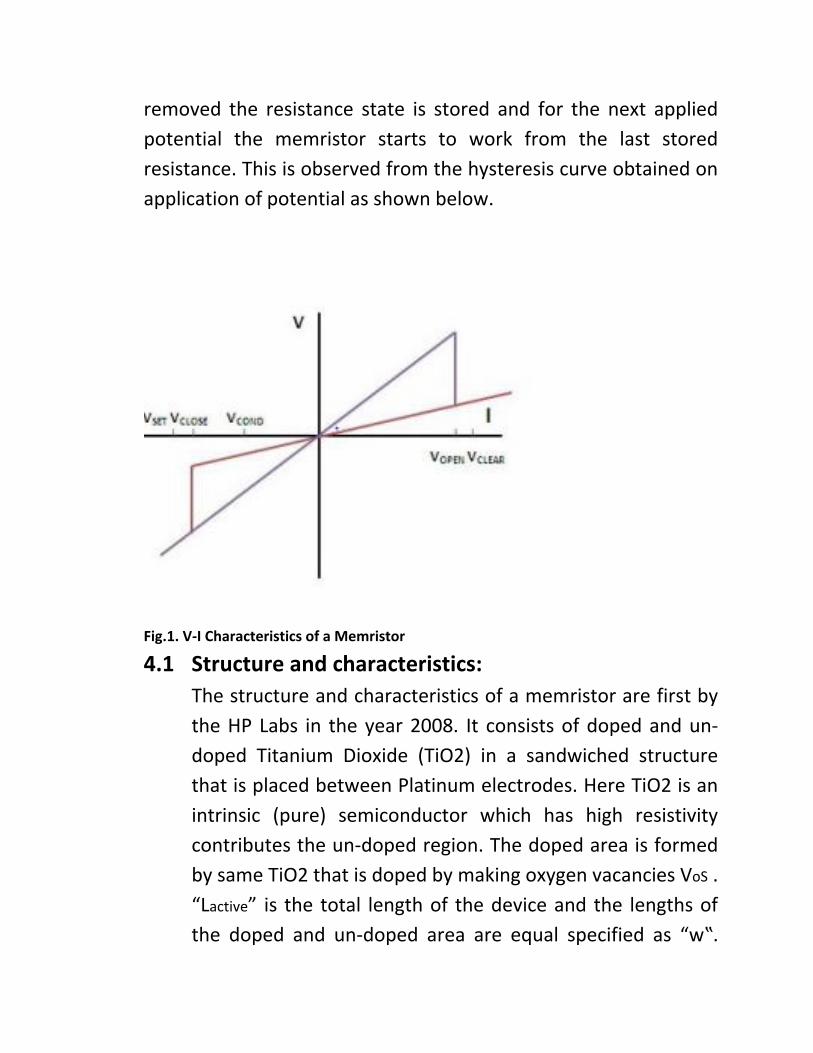
removed the resistance state is stored and for the next applied
potential the memristor starts to work from the last stored
resistance. This is observed from the hysteresis curve obtained on
application of potential as shown below.
Fig.1. V-I Characteristics of a Memristor
4.1 Structure and characteristics:
The structure and characteristics of a memristor are first by
the HP Labs in the year 2008. It consists of doped and un-
doped Titanium Dioxide (TiO2) in a sandwiched structure
that is placed between Platinum electrodes. Here TiO2 is an
intrinsic (pure) semiconductor which has high resistivity
contributes the un-doped region. The doped area is formed
by same TiO2 that is doped by making oxygen vacancies VoS .
“Lactive” is the total length of the device and the lengths of
the doped and un-doped area are equal specified as “w‟.

Also the doped and un-doped areas are considered to be
positive pole and negative pole respectively. Depending on
the time for which the type of charge passing through the
device, the lengths of the doped and un- doped area varies
from ‘w’ which is shown in the following figure.
Fig 2. Structure, Equivalent Resistance and Symbol of a Memristor
Fig.1. V-I Characteristics of a Memristor
The movement of oxygen atoms follows the mechanism of
the dopant drift. i.e., Oxygen vacancies in the TiO2 prefer to

move by rearranging its position on application of potential.
This variation in length of the doped region is specified by “l
doped‟. The boundary line “x” between the doped and un-
doped region shall vary. The variation in the boundary is
provided by the following state equation.
Here “k‟ gives the relation between the mobility ‘μv’ of ions,
R ON, and Lactive. The memristance ‘M’ of the memristor can
be expressed by the following relation.
The memristors have smaller form factor when compared to
other circuit elements including transistors.
Voltage – Current Characteristics of a
Memristor: The following diagram clearly shows the Switching and
Memory phases of a memristor.


Fig 3. V-I Characteristics of a Memristor
Fig.1. V-I Characteristics of a Memristor
The above graph represents the Voltage – Current
characteristics of a memristor. The various sections of the
operation of the memristor can be described as below:
1. The ‘AB’ of the graph depicts and represents the
ON/Closed state of the Memristor – Low resistance Path.
2. The ‘BC’ of the graph depicts and represents the Closed
to Open state of the Memristor.
3. The ‘CD’ of the graph depicts and represents the
OFF/Open state of the Memristor – High resistance Path..
4. The ‘DA’ of the graph depicts and represents the Open to
Close state of the Memristor.
The above four steps can be explained as below.
1. Initially, a set Voltage is applied within a specified voltage
range. When the applied voltage increases beyond Vopen,
Memristor changes from Closed Open.
2. The resistance remains same during the time when
voltage decreases to Zero and the negative voltage
exceeds Vclose.
3. The state of the memristor changes from Open Close.
4. The state of the memristor remains same if the voltage
remains between Vopen and Vclose.
5. The memristor acts as a Switch when the state of the
memristor changes from Open Close and Closed Open.

6. The memristor acts as a Memory when the voltage
remains between Vopen and Vclose.
7. The important property of memristor is that even if the
voltage is removed, it state will be remembered and
applied when a new voltage is applied.
Advantages of Memristors:
1. Requires less voltage.
2. Requires less overall power.
3. Memristor has 2 terminals and Transistor has 3 terminals
which implies it generates less heat.
4. Fast bootup is possible.
Disadvantages of Memristors:
1. Performance of Memristors is less compared to transistors
(Doubted by a few)
2. Speed is 1/11 th of the transistor,
3. Risk of learning wrong methods or patterns.
5. Imply Gate:
1. Imply gate is a digital logic gate used to implement a logical
condition.
2. Imply gate is considered as a virtual gate for memristors.
IMPLY Gate – Traditional Symbol and IEEE symbol.

Traditional Symbol
Truth Table of IMPLY Gate
1. The above traditional IMPLY gate can be represented as
(ab). The output will be (a’+b).
2. a is the ‘Input memristor’ which is negated.
3. b is the ‘Working Memristor’.
4. c is the state of the memristor b after the pulse is applied.
5. The output is available at b.
5.1 Imply Logic Implementation: The implementation of IMPLY logic using two memristors is
as explained below.

Fig.4 IMPLY Logic Implementation
Fig. 5 IMPLY gate realization using a ground resistor
Working of Imply Logic: 1. When P = 0
a. Memristor P =0, implies P is open
b. Memristor P has high resistance

c. The voltage across the grounding resistance is zero.
d. The voltage across memristor Q becomes Vset.
e. From Figure 3, Vset is greater than Vclose causing the
Vset across memristor Q high that implies Vset = 1.
f. The state of Q becomes 1, irrespective of the input at
Q.
2. When P = 1
a. Memristor P=1, implies P is closed.
b. Memristor P has less resistance. P can be treated as a
wire.
c. The voltage across the grounding resistor is same as
Vcond
d. The voltage across memristor Q becomes Vset-Vcond.
e. From Figure 3, Vset-Vcond < Vclose, not enough to switch
the state of Q irrespective of its input.
f. The state of Q = Previous state of Q.
5.2 Imply Logic Sequence Diagram.
The imply sequence logic is used to realize the memristor
circuits as shown below.
1. The horizontal lines represent the memristors.
2. The symbol indicates a pulse being applied to it.
3. The upper side of the symbol shown in the diagram below is
Negated input.
4. The value on the left side of the symbol is the value of
memristor before the pulse.

5. The value on the right side of the symbol is the value of
memristor after the pulse.
6. A zero ‘0’ on the left side indicates an additional pulse
required to reset the input state of the Memristor to 0.
6.1 Min/Max cell – single bit.
Figure 6 - Min/Max Block Diagram
Figure 7 - Min/Max Cell Internal Structure
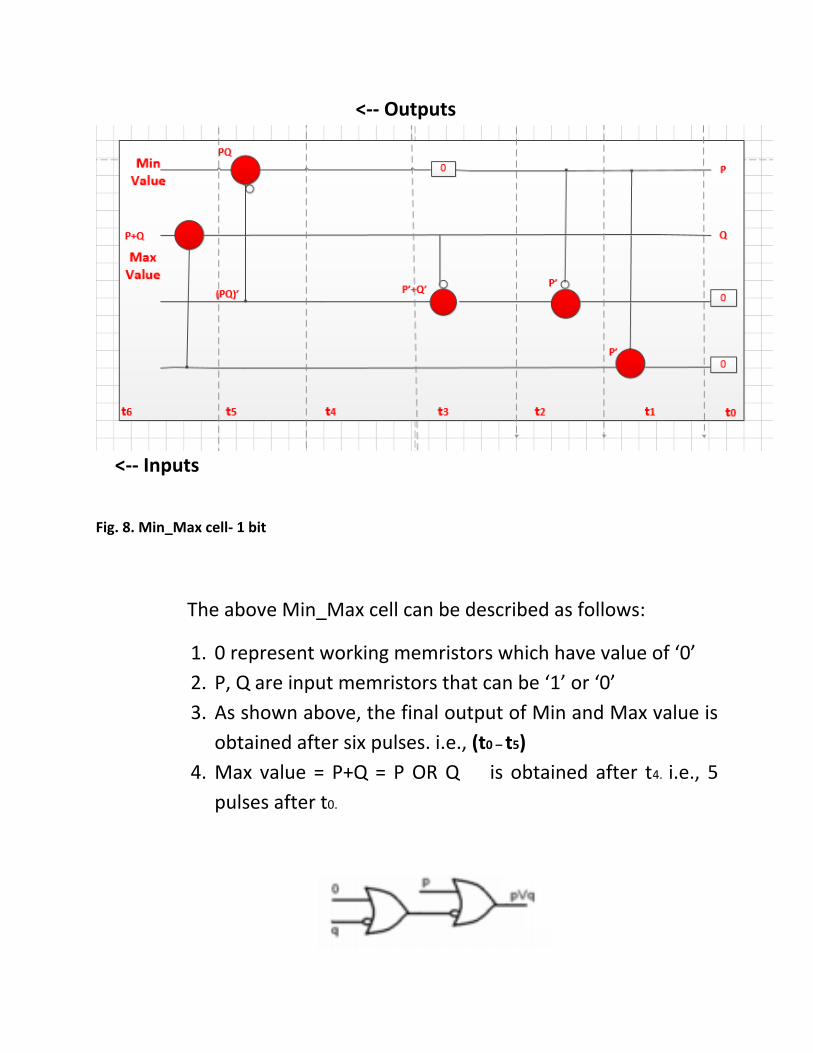
<-- Outputs
<-- Inputs
Fig. 8. Min_Max cell- 1 bit
The above Min_Max cell can be described as follows:
1. 0 represent working memristors which have value of ‘0’
2. P, Q are input memristors that can be ‘1’ or ‘0’
3. As shown above, the final output of Min and Max value is
obtained after six pulses. i.e., (t0 – t5)
4. Max value = P+Q = P OR Q is obtained after t4. i.e., 5
pulses after t0.

5. Min value = P.Q = P AND Q is obtained after t5 i.e., 6
pulses after t0.
6.2 Min_ Max Cell – 4 Bit:

Fig. 9. Min_Max cell- 4 bit
1. The above 4- bit cell can process two 4-bit inputs at a
time.
2. 4-bits in each input can all be given at the same time.
3. The 4 single bit cells are combined to form a single 4-bit
cell.
4. The output is available after 6 pulses for both 1-bit cell
and the 4-bit cell as a whole.

7. Sorting: 1. Sorting is an important operation in engineering
applications. 2. Different types of sorting – Serial and Parallel.
7.1 Serial Sorting: 1. The input bits are forwarded one after the other.
2. Less architecture is required.
3. Waiting time or delay is high.
7.2 Parallel Sorting: 1. The input bits are forwarded all the same time.
2. Heavy architecture (more Min_Max cells) are required.
3. Very less waiting time as It implements a Pipeline model.
8. Implemented Min_Max Cells & Buffers
(Hardware) a. 1-bit Min_Max cell = 24
b. 4- bit Min_Max cell = 6
c. 4-bit 6 register - FIFO Buffers = 4
d. 4- bit 12 register – FIFO Buffer = 12
9. Thermometer Code:

1. Thermometer code is a type of encoding pattern in which
the unsigned integer, n, is represented by n ones and the
remaining zeros until the desired vector width.
2. The Thermometer code makes the comparison easy.
3. Let us take two numbers, say, 2 and 4
4. 2 = 0011 and 4 = 1111 in Thermometer code.
10. Data Flow of a Parallel Sorter – 4-bit
inputs: 1. The data flow of a parallel sorter requires more hardware
when compared to a serial sorter.
2. The time required to get the output is less when compared
to that of the Serial sorter.
3. The two 4-bit inputs are given at the first stage and it takes
6 pulses for the Max and Min values to appear at the output
after comparison.
4. Meanwhile, the inputs at the second stage are already
given and the second stage, now, requires a second input
which is the Min value from the first stage of the pipeline.
5. So, In order not to occur a false comparision, the inputs
given at the second stage are given to a 6 stage-FIFO Buffer
which enables the inputs to reach the 4-bit Min_Max cell
when the Min value from the first stage is readily available.
6. Hence, the parallel sorting using memristive architecture
progresses form here on in the similar fashion.

7. During the third stage, a, 12-bit FIFO Buffer is required to
keep the inputs busy till the Min value form the second
stage is available.
8. So, the parallel triangular sorter implements a Pipeline
model and works in this fashion reducing the overall
throughput time of the outputs.

Memristive Architecture – Parallel Sorter – Full Schematic

11. Delays: 11.1 Input Delay
a. This delay is because of the FIFO buffers that are
required to maintain the 2-D pipeline synchronized.
b. The latency or delay at Cell (0,0) is 1. The Min and
Max are valid for one cycle after inputs 1 and inputs 2
are valid.
c. The latency of cell (1,0) is 6 The Min and Max are
valid for six cycles after inputs 1 and inputs 2 are valid.
d. Similarly, latency of the cell (2,0) is 12. The Min and
Max are valid for 12 cycles after inputs 1 and inputs 2
are valid.
e. These are input delays.
11.2 Output Delay
The output delays are required for synchronization at the
output.
11.3 Corner Delay
A corner delay is required while the output from the
right most cell of each row goes to the next higher cell.
Applications:
1. Sorter circuits find application while working with a lot
of large data sets.
2. A sorted array or data is much easier to understand

3. Sorted data is useful in extracting meaningful insights
from unstructured or structured data.
4. Sorting detects the redundancy in a large circuit with m
n-bit inputs.
5. Very significant role and is going to be useful in the near
future in the areas of Data Science, Machine Learning,
etc.
HDL Code and Timing/Simulation Diagram.
a. Memristor.v
module Memristor
# (
parameter N=4)
(
input reg [N-1:0] neg_inp,
input reg [N-1:0] memristor_inp,
output wire [N-1:0] memristor_out
);
assign memristor_out = (~neg_inp) | memristor_inp;
endmodule
b. Parallel Min_Max.v
module ParallelMinMax
# (
parameter N=4
)
(
input reg clk, rst,
input reg [N-1:0] a,
input reg [N-1:0] b,
output wire [N-1:0] min,
output wire [N-1:0] max
);

reg [N-1:0] C_and;
reg [N-1:0] C_or;
always@(posedge clk)
begin
if (rst)
begin
C_and <= '0;
C_or <= '0;
end
else begin
//min value calculation by AND operation
C_and[0] = a[0] & b [0];
C_and[1] = a[1] & b [1];
C_and[2] = a[2] & b [2];
C_and[3] = a[3] & b [3];
// max value calculation by OR operation
C_or[0] = a[0] | b [0];
C_or[1] = a[1] | b [1];
C_or[2] = a[2] | b [2];
C_or[3] = a[3] | b [3];
end
end
assign min = C_and;
assign max = C_or;
endmodule
c. Min_Max_Memristor.v
module Min_Max_memristor
#(
parameter N=4,
parameter M=4
)
(
input clk, rst,
input [3:0] a,
input [3:0] b,
output reg [3:0] min,
output reg [3:0] max
);
wire [3:0] c;
wire [3:0] c1;

wire [3:0] c2;
wire [3:0] c3;
wire [3:0] c4;
reg [3:0] zero = 4'b0000;
always @ (posedge clk or posedge rst)
begin
if (rst) begin
min<= 0;
max<= 0;
end
else begin
max<= c1;
min<= c4;
end
end
Memristor OR1(
.neg_inp(a),
.memristor_inp(zero),
.memristor_out(c));
Memristor OR2(
.neg_inp(c),
.memristor_inp(b),
.memristor_out(c1));
Memristor AND1(
.neg_inp(a),
.memristor_inp(zero),
.memristor_out(c2));
Memristor AND2(
.neg_inp(b),
.memristor_inp(c2),
.memristor_out(c3));
Memristor AND3(
.neg_inp(c3),
.memristor_inp(zero),
.memristor_out(c4));
Endmodule
f. Sorter_tb

`timescale 1ns/1ps
module Sorter_TB();
parameter N=4; // individual input width
parameter M=5; // number of inputs
reg [3:0] A, B, C, D;
wire [3:0] P, Q, R, S;
reg clk;
reg rst;
initial clk = 1;
always #10 clk = ~clk;
parallel_sorter #(
.N (N),
.M (M)
) sort (
.clk (clk),
.rst (rst),
.A (A),
.B (B),
.C (C),
.D (D),
.P (P),
.Q (Q),
.R (R),
.S (S)
);
initial begin
rst = 1'b1;
#5 rst = ~rst;
$display("\n");
$display("time\trst\tA\tB\tC\tD\t\t\P\tQ\tR\tS");
$display("============================================");
$monitor("%2d\t%0d\t%p\t%p\t%p\t%p\t%p\t%p\t%p\t%p", $time, rst, A, B, C, D,
P, Q, R, S);
//$display("%2d\t%0d\t%p\t%p", $time, rst, X, Y);
@(negedge clk); A = 4'h15; B = 4'h0; C = 4'h7; D = 4'h3 ;
//$display("%2d\t%0d\t%p\t%p", $time, rst, X, Y);
//@(negedge clk) X = '{M{0}};
/*
//$display("%2d\t%0d\t%p\t%p", $time, rst, X, Y);
#10 X = '{8,7,7,5,1};
//$display("%2d\t%0d\t%p\t%p", $time, rst, X, Y);

#10 X = '{4,1,2,3,8};
//$display("%2d\t%0d\t%p\t%p", $time, rst, X, Y);
#10 X = '{1,8,3,2,8};
//$display("%2d\t%0d\t%p\t%p", $time, rst, X, Y);
#10 X = '{0,0,1,1,8};
//$display("%2d\t%0d\t%p\t%p", $time, rst, X, Y);
#10 X = '{8,8,8,8,8};
//$display("%2d\t%0d\t%p\t%p", $time, rst, X, Y);
*/
#1000
$display("============================================");
$display("\n\n");
$stop;
end
endmodule
Shift_register.v
module shiftregister
#(
parameter N=4, // width
parameter M=4 // depth
)(
input reg Clk,Clr,
input reg [N-1:0] SRI,
output wire [N-1:0] SRO
);
integer i;
reg [N-1:0] C [M-1:0];
always@(posedge Clk) begin
if (Clr)
begin
for (i=0;i<M;i=i+1)
begin
C[i] <= 0;
end
end
else
begin
for (i=0;i<M-1;i=i+1)

begin
C[i+1] <= C [i];
C[0] <= SRI;
end
end
end
assign SRO = C [M-1];
endmodule
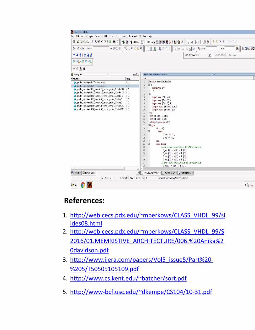
Timing Diagrams

References:
1. http://web.cecs.pdx.edu/~mperkows/CLASS_VHDL_99/slides08.html
2. http://web.cecs.pdx.edu/~mperkows/CLASS_VHDL_99/S
2016/01.MEMRISTIVE_ARCHITECTURE/006.%20Anika%2
0davidson.pdf
3. http://www.ijera.com/papers/Vol5_issue5/Part%20-
%205/T50505105109.pdf
4. http://www.cs.kent.edu/~batcher/sort.pdf
5. http://www-bcf.usc.edu/~dkempe/CS104/10-31.pdf