edacs vertical turbo card roa 117 2239 - … · edacs vertical turbo card roa 117 2239 ... 96 pin...
TRANSCRIPT
ericssonzericssonz
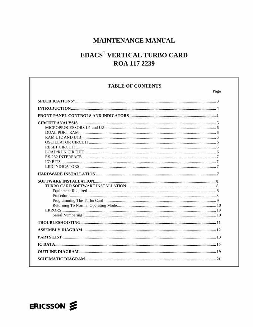
MAINTENANCE MANUAL
EDACS VERTICAL TURBO CARDROA 117 2239
TABLE OF CONTENTSPage
SPECIFICATIONS*....................................................................................................................................... 3
INTRODUCTION........................................................................................................................................... 4
FRONT PANEL CONTROLS AND INDICATORS ................................................................................... 4
CIRCUIT ANALYSIS .................................................................................................................................... 5MICROPROCESSORS U1 and U2 ........................................................................................................... 6DUAL PORT RAM ................................................................................................................................... 6RAM U12 AND U13 ................................................................................................................................. 6OSCILLATOR CIRCUIT.......................................................................................................................... 6RESET CIRCUIT ...................................................................................................................................... 6LOAD/RUN CIRCUIT .............................................................................................................................. 6RS-232 INTERFACE ................................................................................................................................ 7I/O BITS .................................................................................................................................................... 7LED INDICATORS................................................................................................................................... 7
HARDWARE INSTALLATION ................................................................................................................... 7
SOFTWARE INSTALLATION..................................................................................................................... 8TURBO CARD SOFTWARE INSTALLATION...................................................................................... 8
Equipment Required ........................................................................................................................... 8Procedure............................................................................................................................................ 8Programming The Turbo Card............................................................................................................ 9Returning To Normal Operating Mode............................................................................................... 10
ERRORS.................................................................................................................................................... 10Serial Numbering................................................................................................................................ 10
TROUBLESHOOTING.................................................................................................................................. 11
ASSEMBLY DIAGRAM................................................................................................................................ 12
PARTS LIST ................................................................................................................................................... 13
IC DATA.......................................................................................................................................................... 15
OUTLINE DIAGRAM ................................................................................................................................... 19
SCHEMATIC DIAGRAM ............................................................................................................................. 21

AE/LZB 119 1887 R1A
2
Copyright Sepotember 1996, Ericsson Inc.
FIGURES AND TABLES
Figure 1 - Vertical Turbo Card Front Panel ...............................................................................................4Figure 2 - Turbo Card Block Diagram .......................................................................................................5Figure 3 - Memory Map For Each DS-2250 ..............................................................................................6Figure 4 - Trunking Card PC Programmer Load File Menu.......................................................................8Figure 5 - Turbo Card Programming..........................................................................................................9
Table 1 - Connector Chart ..........................................................................................................................5
AE/LZB 119 1887 R1A
3
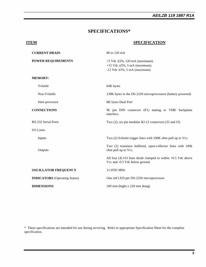
SPECIFICATIONS*
ITEM SPECIFICATION
CURRENT DRAIN 80 to 120 mA
POWER REQUIREMENTS +5 Vdc ±5%, 120 mA (maximum).+12 Vdc ±5%, 5 mA (maximum).-12 Vdc ±5%, 5 mA (maximum).
MEMORY:
Volatile
Non-Volatile
Inter-processor
64K bytes
128K bytes in the DS-2250 microprocessors (battery powered)
8K bytes Dual Port
CONNECTIONS
RS-232 Serial Ports
I/O Lines:
Inputs
Outputs
96 pin DIN connector (P1) mating to VME backplaneinterface.
Two (2), six pin modular RJ-12 connectors (J2 and J3)
Two (2) Schmitt trigger lines with 100K ohm pull up to Vcc.
Two (2) transistor buffered, open-collector lines with 100kohm pull up to Vcc.
All four (4) I/O lines diode clamped to within +0.5 Vdc aboveVcc and -0.5 Vdc below ground.
OSCILLATOR FREQUENCY 11.0592 MHz
INDICATORS (Operating Status) One red LED per DS-2250 microprocessor
DIMENSIONS 100 mm (high) x 220 mm )long)
* These specifications are intended for use during servicing. Refer to appropriate Specification Sheet for the completespecification.
AE/LZB 119 1887 R1A
4
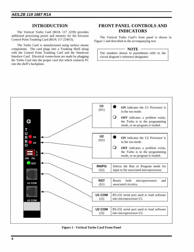
INTRODUCTIONThe Vertical Turbo Card (ROA 117 2239) provides
additional processing power and memory for the EricssonControl Point Trunking Card (ROA 117 2240/3).
The Turbo Card is manufactured using surface mountcomponents. The card plugs into a Trunking Shelf alongwith the Control Point Trunking Card and the SimulcastInterface Card. Electrical connections are made by pluggingthe Turbo Card into the proper card slot which connects P1into the shelf’s backplane.
FRONT PANEL CONTROLS ANDINDICATORS
The Vertical Turbo Card’s front panel is shown inFigure 1 and described in the accompanying text.
NOTE
The numbers shown in parentheses refer to thecircuit diagram’s reference designator.
Figure 1 - Vertical Turbo Card Front Panel
U1(D1)
® ON indicates the U1 Processor isin the run mode.
m OFF indicates a problem exists,the Turbo is in the programmingmode, or no program is loaded.
U2(D2)
® ON indicates the U2 Processor isin the run mode.
m OFF indicates a problem exists,the Turbo is in the programmingmode, or no program is loaded.
RN/PG(S2)
Selects the Run or Program mode forinput to the associated microprocessor.
RST(S1)
Resets both microprocessors andassociated circuitry.
U1 COM(J2)
RS-232 serial port used to load softwareinto microprocessor U1.
U2 COM(J3)
RS-232 serial port used to load softwareinto microprocessor U2.
U1
U2
TURBO
U2 COM
U1 COM
RST
RN PG
12
NOTE

AE/LZB 119 1887 R1A
5
Table 1 - Connector Chart
Connector Description
P1 Turbo Card's interface to theTrunking Card’s address/data bus &power and U1, U2 input/output.
J2 (U1 COM) RS-232 serial interface to U1
J3 (U2 COM) RS-232 serial interface to U2
CIRCUIT ANALYSISThe Turbo Card consists of two independent
microprocessor sections (See Figure 2). The heart of eachsection is a DS-2250 microprocessor, U1 or U2. In additionto its internal memory, each microprocessor has a 32K byteexternal RAM, U12 or U13. Each section also contains a4K byte Dual Port RAM (DPRAM), U3 or U4, whichprovides the interface to the Trunking Card. A singleoscillator, consisting of U14 and B1, provides the clock forboth processors. Each processor uses one half of U8 tointerface between its TTL I/O and its RS-232 serial port.When one of the processors triggers U9, it turns on eitherLED D1 or D2. A single input bit and a single output bit isavailable on each processor for I/O. The module has asingle RESET button which resets both processors.LOAD/RUN circuits on each processor set the operatingmode. Port 1 and INT 0 of both processors are tied togetherto provide a high speed parallel communication linkbetween the two processors.
U2
DS-2250
U1
DS-2250
P1
P1
Y1
32kRAMU13
4kDPRAM
U4
4kDPRAM
U3
Microprocessor
GETC
BUS
32kRAMU12
OSC
U14-A,B
U15-B
BUFFER
Q10
One-Shot
U9-B
U9-A
One-Shot
U15-A
Q9
BUFFER
Load/Run
RESET
Circuit
INTFC1/2 U8
RS-232
SerialPort
IN
OUT
INTFC
1/2 U8
RS-232
SerialPort
IN
OUT
D1
D2
Figure 2 - Turbo Card Block Diagram

AE/LZB 119 1887 R1A
6
MICROPROCESSORS U1 and U2
Microprocessors U1 and U2 are Dallas SemiconductorDS-2250 single-in-line package (SIP) modules. TheDS-2250 is a special proprietary derivative of the Intel 8031microprocessor containing the basic 8031 structure, abootstrap loader, terminal interface, and internal control of64K bytes of battery backed-up RAM. The RAM can bepartitioned into two separate code and data areas, The codearea can be write protected after it is initially loaded. Aninternal bit, ECE2, under program control alters the memorymap allowing access to all available memory (see Figure 3).
DUAL PORT RAM
Dual-port RAM (DPRAM) chips U3 and U4 interfacewith the Trunking Card's 8032 microprocessor (U1). OneDPRAM port is connected to the Trunking Card and theother port is connected to either U1 or U2. To the TrunkingCard, U3 and U4 appear as a single 8k byte memory blockbetween addresses 0 and 1FFFH. To the Turbo Cardmicroprocessor U1, U3 appears as a 4k byte RAMaddressed from 0 to 0FFFH and likewise, U2 sees U4 as a4k byte RAM addressed from 0 to 0FFFH. Thus, eachmicroprocessor shares 4K bytes of memory with theTrunking Card processor. This permits the efficientexchange of data between the Trunking Card and the TurboCard. Integrated circuits U11-D and U10-D drive the outputenable (read) input (RAM CS) from the Trunking Card,while U10-A, B, and C along with U11-A and B driveDPRAM chip enables origninating from the Trunking Cardwrite command (WRBAR).
RAM U12 AND U13
As shown in Figure 3, when ECE2 is 0, each processoraccesses a 32K RAM at addresses 8000H to FFFFH. TheseRAM's are on the Turbo Card, not in the DS-2250, thus theyare not powered by the DS-2250 battery. This volatile
memory space is used as a temporary scratch pad by theprocessors. U10-E and U10-F drive the RAM CE (chipenable), pins of U12 and U13 respectively, from bit 15 ofthe address bus. A low enables the RAM.
OSCILLATOR CIRCUIT
U14 is an unbuffered CMOS inverter (74HCU04). Inthis application, U14-A functions as a linear gain stage withcrystal B1 in its feedback path, forming an oscillator at11.0592 MHz. U14-B buffers the clock and drives bothprocessors' clock input pins.
RESET CIRCUIT
Switch S1 resets the Turbo Card and the TrunkingCard's S4 resets the Trunking Card. The software willusually start properly with only an S4 Trunking Card reset;however, both boards may be reset
Depressing the Turbo Card's S1 grounds R21, R22, andthe positive side of C21. This turns on PNP transistors Q4and Q7 pulling the RESET input of each processor high. Inthis logic state, the microprocessors are reset and notoperating. When S1 is released, the voltage on C21'spositive terminal and the bases of Q4 and Q7 slowly rises asC21 charges through R8, R15, R21, and R22. Eventually,this voltage rises high enough to turn Q4 and Q7 offallowing the processor RESET inputs to fall low. RESET iskept low at this point by R7 and R14. R8 and R15 hold Q4and Q7 in the off condition.
LOAD/RUN CIRCUIT
During normal operation (RUN mode), the processors'RESET inputs are held low and the PSEN output controlsexternal memory. Each DS-2250 is put into the LOADmode by holding its RESET pin high and pulling its PSEN
ECE2 = 1FFFF=64k
NOTHING
U12 & U13
8000H
TOP RAM(INSIDE DS-2250)
PARTITION
0
CODESPACE
ECE2 = 0FFFF=64k
DPRAM FOLDED
8000H
6800H
1000H
0
EXT RAM
BOTTOM RAM(INSIDE DS-2250)
Figure 3 - Memory Map For Each DS-2250

AE/LZB 119 1887 R1A
7
pin low.
Switch S2 selects RUN/LOAD mode for processor U1.Moving S2 down shorts pins 2 and 3, placing U1 in theLOAD mode. This applies Vcc (5V) to R10 and R12. Vccon R10 turns on Q8 which turns on Q7 through R9 pullingU1's RESET high. Vcc on R12 turns on Q6 which holdsPSEN low. When S2 is up (shorting pins 1 and 2) theprocessor is in the RUN mode. Vcc is not applied to R10and R12. Q8 is held off by R11 and Q7 is held off by R8 soRESET is pulled low by R7. Q6 is held off by R13 soPSEN is not held low and may become an output of U1.
Switch S3 selects RUN/LOAD mode for processor U2.Moving S3 down shorts pins 2 and 3, placing U2 in theLOAD mode. This applies Vcc (5V) to R17 and R19. Vccon R17 turns on Q5 which turns on Q4 through R16 pullingU2's RESET high. Vcc on R19 turns on Q3 which holdsPSEN low. When S3 is up (shorting pins 1 and 2) theprocessor is in the RUN mode. Vcc is not applied to R17and R19. Q5 is held off by R18 and Q4 is held off by R15so RESET is pulled low by R4. Q3 is held off by R20 soPSEN is not held low and may become an output of U2.
RS-232 INTERFACE
The RS-232 interfaces are used to program theDS-2250 modules and to interface to other serial devices infuture applications (refer to the Programming Instructions).An Intel hex format file from a PC can be loaded intomemory via the serial ports. This manual and the SoftwareRelease Notes (SRN) provide complete instructions forloading software in the field.
U8 is a dual TTL-to-RS-232 duplex serial interface.Capacitors C1, C2, C3, and C4 are used by U8 to convert5V signals to RS-232 levels. Section 1 converts U1's serialport to RS-232 and section 2 converts U2's serial port to RS-232. The serial output for U1 is at J2-2 and the input is atJ2-1. The serial output for U2 is at J3-2 and the input is atJ3-1.
I/O BITS
One output bit from U1 is available. It is buffered byQ9 and drives out on P1-B21. Weak pull-up R30 holds P1-B21 high when Q9 is turned off by U1. One input bit to U1
is available. It is buffered from P1-B20 by U15-A andprotected from static and overdrive by D3 and R27. Weakpull-up R35 holds the input high when not in use.
One output bit from U2 is available. It is buffered byQ10 and drives out on P1-B23. Weak pull-up R32 holds JP1-B23 high when Q10 is turned off by U2. One input bit toU2 is available. It is buffered from P1-B22 by U15-B andprotected from static and overdrive by D4 and R31. Weakpull-up R36 holds the input high when not in use.
LED INDICATORS
LED D1 is controlled by processor U1. The processormust apply pulses to retriggerable one-shot (monostablemultivibrator) U9 pin 4 about every half second or faster tokeep the LED on. This provides a visual indication that themicroprocessor is running. The pulse on U9-4 retriggers theoutput on U9-6 keeping Q1 on and LED D1 on. If thepulses don't appear before the one-shot times out, U9-6 willfall low turning Q1 and D1 off. R1 and C17 determine thedrop-out time.
LED D2 is controlled by processor U2. The processormust apply pulses to retriggerable one-shot (monostablemultivibrator) U9 pin 12 about every half second or faster tokeep the LED on. This provides a visual indication that themicroprocessor is running. The pulse on U9-12 retriggersthe output on U9-10 keeping Q2 on and LED D2 on. If thepulses don't appear before the one-shot times out, U9-10 willfall low turning Q2 and D2 off. R4 and C18 determine thedrop-out time.
HARDWARE INSTALLATIONInstallation or removal of the Turbo Card involves
sliding the assembly into or out of the VME Shelf. Thismay be accomplished with power applied without damagingthe assembly.
When installing the Turbo Card, ensure the card isinstalled in the designated slot. Refer to the specificapplication drawings.
AE/LZB 119 1887 R1A
8
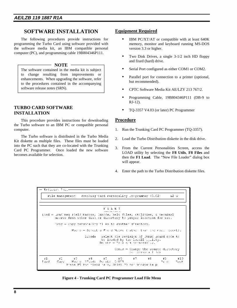
SOFTWARE INSTALLATIONThe following procedures provide instructions for
programming the Turbo Card using software provided withthe software media kit, an IBM compatible personalcomputer (PC), and programming cable 19B804346P111.
NOTE
The software contained in the media kit is subjectto change resulting from improvements orenhancements. When upgrading the software, referto the procedures contained in the accompanyingsoftware release notes (SRN).
TURBO CARD SOFTWAREINSTALLATION
This procedure provides instructions for downloadingthe Turbo software to an IBM PC or compatible personalcomputer.
The Turbo software is distributed in the Turbo MediaKit diskette as multiple files. These files must be loadedinto the PC such that they are co-located with the TrunkingCard PC Programmer. Once loaded the new softwarebecomes available for selection.
Equipment Required
• IBM PC/XT/AT or compatible with at least 640Kmemory, monitor and keyboard running MS-DOSversion 3.3 or higher.
• Two Disk Drives, a single 3-1/2 inch HD floppyand fixed (hard) drive.
• Serial Port configured as either COM1 or COM2.
• Parallel port for connection to a printer (optional,but recommended).
• CPTC Software Media Kit AE/LZY 213 767/2.
• Programming Cable, 19B804346P111 (DB-9 toRJ-12).
• TQ-3357 V4.03 (or later) PC Programmer
Procedure
1. Run the Trunking Card PC Programmer (TQ-3357).
2. Load the Turbo Distribution diskette in the disk drive.
3. From the Current Personalities Screen, access theLOAD utility by selecting the F8 Utils, F8 Files andthen the F1 Load. The “New File Loader” dialog boxwill appear.
4. Enter the path to the Turbo Distribution diskette files.
ÚÄ Ericsson Inc.ÄÄÄÄÄÄÄÄÄÄÄÄÄÄÄÄÄÄÄÄÄÄÄÄÄÄÄÄÄÄÄÄÄÄÄÄÄÄÄÄÄÄÄÄÄÄÄÄÄÄÄÄÄÄÄÄÄÄÄÄÄÄÄ¿³ÚÄÄÄÄÄÄÄÄÄÄÄÄÄÄÄÄÄÄÄÄÄÄÄÄÄÄÄÄÄÄÄÄÄÄÄÄÄÄÄÄÄÄÄÄÄÄÄÄÄÄÄÄÄÄÄÄÄÄÄÄÄÄÄÄÄÄÄÄÄÄÄÄÄÄÄÄ¿³³³ File Management Trunking Card Personality Programmer (5.02) L2ÄG ³³³ÀÄÄÄÄÄÄÄÄÄÄÄÄÄÄÄÄÄÄÄÄÄÄÄÄÄÄÄÄÄÄÄÄÄÄÄÄÄÄÄÄÄÄÄÄÄÄÄÄÄÄÄÄÄÄÄÄÄÄÄÄÄÄÄÄÄÄÄÄÄÄÄÄÄÄÄÄÙ³ÀÄÄÄÄÄÄÄÄÄÄÄÄÄÄÄÄÄÄÄÄÄÄÄÄÄÄÄÄÄÄÄÄÄÄÄÄÄÄÄÄÄÄÄÄÄÄÄÄÄÄÄÄÄÄÄÄÄÄÄÄÄÄÄÄÄÄÄÄÄÄÄÄÄÄÄÄÄÄÙÚÄÄÄÄÄÄÄÄÄÄÄÄÄÄÄÄÄÄÄÄÄÄÄÄÄÄÄÄÄÄÄÄÄÄÄÄÄÄÄÄÄÄÄÄÄÄÄÄÄÄÄÄÄÄÄÄÄÄÄÄÄÄÄÄÄÄÄÄÄÄÄÄÄÄÄÄÄÄ¿³ F I L E S ³³ ~~~~~~~~~ ³³ Load Ä Load new Field Macros, 1Ecode, help files, utilities, & terminal ³³ macros from other disk or directory to proper location for use. ³³ ³³ Copy Ä copy personality files to another directory. ³³ ³³ Macro Ä Select a Field Macro (rather than the most recent). ³³ ³³ 1Ecode Ä Select the revision of TURBO Board code to ³³ be loaded by the Load1E utility. ³³ Delete Ä Delete a personality. ³³ ³³ ChDIR Ä Change the source directory ³³ for personalities ³ÀÄÄÄÄÄÄÄÄÄÄÄÄÄÄÄÄÄÄÄÄÄÄÄÄÄÄÄÄÄÄÄÄÄÄÄÄÄÄÄÄÄÄÄÄÄÄÄÄÄÄÄÄÄÄÄÄÄÄÄÄÄÄÄÄÄÄÄÄÄÄÄÄÄÄÄÄÄÄÙ F1 F2 F3 F4 F5 F6 F7 F8 F9 F10 Load Copy Macro 1Ecode Delete ChDIR Help Back Press F9 for field help, Shift F9 for window help
Figure 4 - Trunking Card PC Programmer Load File Menu
NOTE

AE/LZB 119 1887 R1A
9
5. The programmer will load all files , including the FieldMacros into the PC Programmer’s working directories.
6. It is now possible to program the Turbo Card.
Programming The Turbo Card
This procedure downloads the Turbo software to themicroprocessors U1 and U2 on the Turbo board.
NOTE
Re-programming the Turbo Card will not alterpreviously stored Personality Data. WhenPersonality Data is present, “load1e.exe” clearsand performs CRC functions over the code portionof memory only. The “load1e.exe” also storesCRC data in the DS-2250's memory for future datacorruption checks.
1. Refer to TQ-3357 Chapter 4 - Upgrading Firmwarewith the Load1E Utility for complete instructions ondownloading the Turbo software .
2. Connect the Programming Cable, 19B804346P111,from the PC's serial port connector to the Turbo cardinput port connector U1 COM (see Figure 5).
NOTE
References in the Trunking Card PC Programmerto J103 and J104 refer to connectors U1 COM (J2)and U2 COM (J3), respectively.
3. With power ON, move the Turbo Card RN/PG switchesto the PG position (toward the right). This places theprocessors U1 and U2 into the programming mode. Ifeither switch is already in the PG position, move theswitch to the RN position and then back to the PGposition.
NOTE
References in the Trunking Card PC Programmerto switches S2 and S3 correspond to DIP Switch S2sections 1 and 2, respectively. When directed tomove the switches to the “front” or programmingmode, move the switch to PG. When directed tomove the switches to the “rear” or run mode, movethe switches to RN.
4. The Turbo Card LEDs U1 (D1) and U2 (D2) shouldturn OFF indicating that the Turbo Card is in theprogramming mode.
5. Execute the "load1e.exe" program on the PC andfollow the on screen instructions.
6. The "load1e.exe" program loads the file "1etop.hex"
ToCOM Port
Software Disk
Contains The LOAD1EFile Transfer Utilit yand Turbo Board'sExecutable Code
U1
U2
TURBO
U2 COM
U1 COM
RST
RN PG
12
Programming Cable19B803346P111
TQ3357
Figure 5 - Turbo Card Programming
NOTE
NOTE
NOTE
AE/LZB 119 1887 R1A
10
into the Turbo Card's upper half of memory for use bythe processor U1.
7. Monitor the PC's on screen instructions and prompts.
8. When directed, move the programming cable from theU1 COM connector to U2 COM.
9. After the cable is moved to U2 COM, the PC willindicate it is loading the "1ebot.hex" file into the TurboCard's lower half of memory for use by the processorU2.
10. Disconnect the programming cable upon successfulcompletion of the programming procedure and returnthe Turbo Card to the Normal operating mode.
Returning To Normal Operating Mode
Upon successful completion of the programming, thePC displays a "FINISHED - SWITCH S2 AND S3 TOTHE REAR " message.
1. Move the Turbo Card RN/PG switches to the RNposition (toward the left). This places the processorsU1 and U2 into the run mode.
2. Press S1 to reset the Turbo Card.
3. The Turbo Card LEDs, U1 (D1) and U2 (D2), will lightindicating the code is executing.
4. This completes the Turbo Card programming. If anyproblems were encountered or if any error messageswere received, refer to the Error section below orTrouble Shooting section of this manual.
ERRORS
The transfer process uses the file 1ECRC.HEX for errorchecking and verification. Any error during this proceduregenerally indicates a defective communication link betweenthe PC and Turbo Card. If errors occur, check connectorsand cables. Cycle the RN/PG switch from the PG to RNand back to PG. Repeat the programming sequence.
Errors usually generate one or more of the following:
• Error 1 Did not receive sign-on banner fromDS-2250.
• Error 2 Did not receive CR-LF from DS-2250.
• Error 3 Did not receive prompt from DS-2250.
• Error 4 Did not receive CRC value from DS-2250.
• Error 5 Did not receive serial number fromDS-2250.
"Cannot open COM Port" - The PC's COM Port is non-existent or in use by other software or hardware. A PC re-configuration is required.
"Cannot open 'filename' " - Be sure file exists in theappropriate directory.
"Bad CRC" - A CRC error means that after loading,memory contents are incorrect or the wrong "1ecrc.Hex"file was used. If the "1ecrc.Hex" file is the same shippedwith the software, a Turbo Card hardware problem isindicated.
"Wrong serial number-check cables" - If cabling iscorrect, DS-2250 microprocessors may have been swapped.The four byte serial number is printed to the screen to helpin restoring DS-2250's to their proper locations. The serialnumbers will be the same, except for least significant bit, forboth DS-2250's The least significant bit must be logic 1 forthe top DS-2250 (U1) and logic 0 for the bottom DS-2250(U2).
"Illegal serial number" - Serial number is either invalid,was never programmed, or has been erased.
Serial Numbering
An error will occur when U1 and U2 are swapped.Each processor has a unique serial number with U1 havingan odd serial number and U2 having a serial number onedigit less than U1’s serial number. The PC’s on screeninformation displays the processors’ serial numbers forverification. The most significant digits of U1 and U2’sserial numbers must match.
Do not swap U1 and U2 DS2250 microprocessors ortake one DS-2250 from one Turbo Card and put it in anotherTurbo Card. However, it is permissible to swap DS-2250'sas pairs if the U1 and U2 positions are maintained.
AE/LZB 119 1887 R1A
11
TROUBLESHOOTINGIf a problem is traced to the Turbo Card, perform the
following checks and inspections:
• If an error message is received while loading theTurbo Card software, review ProgrammingInstructions - Errors section for possible correctiveaction.
• Visually check for damaged parts, unsoldered pinsor parts, broken cable or pins (P1), or unseated DS-2250 modules.
• Look for trash in the SIP sockets. A magnifyingglass or low power microscope is helpful.
• Verify the RN/PG switch is in the RN position inthe RUN condition.
• Check +5, +12 and -12 volt lines.
• With a high speed, high impedance scope, checkfor oscillations at U14-4. A somewhat flattenedsine wave of about 4V amplitude at 11.0592 MHzshould be seen.
If the problem persists, substitute the Turbo Card with aknown good Turbo Card. Ensure the substitute card has thecorrect software loaded.
If the DS-2250 modules are suspect, substitute themodules with modules from a known good board. Be sureto put U1 from the good Turbo Card into XU1 of the suspectTurbo Card and likewise for U2. Remember to swap DS-2250's as pairs and reprogram the Turbo card if necessary.
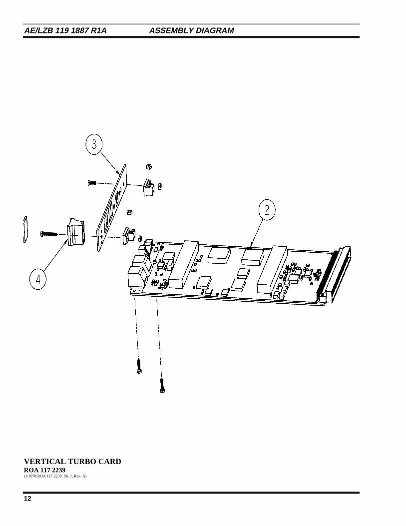
AE/LZB 119 1887 R1A ASSEMBLY DIAGRAM
12
VERTICAL TURBO CARDROA 117 2239(1/1078 ROA 117 2239, Sh. 1, Rev. A)

PARTS LIST AE/LZB 119 1887 R1A
13
VERTICAL TURBO CARD131 32-ROA 117 2239
Revision: D
Symbol PART NUMBER DESCRIPTION
------------------------ CRYSTAL ----------------------
B1 RTM 501 658/01 11.0592 MHz
---------------------- CAPACITOR --------------------
C1 RJE 584 3168/47 Tantalum Chip: 47 µF 16V Case D
C10 RJC 464 3045/1 10nF 0805 50V ±10%
C11 RJC 464 3045/1 10nF 0805 50V ±10%
C12 RJC 464 3045/1 10nF 0805 50V ±10%
C13 RJC 464 3045/1 10nF 0805 50V ±10%
C14 RJC 464 3045/1 10nF 0805 50V ±10%
C15 RJC 464 3045/1 10nF 0805 50V ±10%
C16 RJC 464 3045/1 10nF 0805 50V ±10%
C17 RJE 584 3107/22 Tantalum Chip: 2.2 µF 10V Case A
C18 RJE 584 3107/22 Tantalum Chip: 2.2 µF 10V Case A
C19 RJC 463 4042/27 27pF 0805 50V ±5%
C2 RJE 584 3168/47 Tantalum Chip: 47 µF 16V Case D
C20 RJC 463 4042/27 27pF 0805 50V ±5%
C21 RJE 584 3207/1 Tantalum Chip: 1 µF 20 v case a
C22 RJC 464 3045/1 10nF 0805 50V ±10%
C23 RJC 464 3045/1 10nF 0805 50V ±10%
C24 RJC 464 3045/1 10nF 0805 50V ±10%
C25 RJC 464 3045/1 10nF 0805 50V ±10%
C26 RJC 464 3045/1 10nF 0805 50V ±10%
C3 RJE 584 3168/47 Tantalum Chip: 47 µF 16V Case D
C5 RJE 584 3168/47 Tantalum Chip: 47 µF 16V Case D
C6 RJC 464 3045/1 10nF 0805 50V ±10%
C7 RJC 464 3045/1 10nF 0805 50V ±10%
C8 RJC 464 3045/1 10nF 0805 50V ±10%
C9 RJC 464 3045/1 10nF 0805 50V ±10%
------------------------- DIODES -----------------------
D1 RKZ 433 637/1 LED: 90 degree. Red
D2 RKZ 433 637/1 LED: 90 degree. Red
D3 RKZ 123 03/1 Dual switching, in series
D4 RKZ 123 03/1 Dual switching, in series
-------------------------- FUSES ------------------------
F1 REZ 701 16/2 Thermistor Circuit Protector: 0.5A 60V PTC.
F2 REZ 701 28/1 Thermistor Circuit Protector: 0.5A 15V PTC.
F3 REZ 701 28/1 Thermistor Circuit Protector: 0.5A 15V PTC.
-------------------------- JACKS ------------------------
J2 RNV 403 19/06 Fork Contact Unit: MMP-JACK VINKLAT 6/6
J3 RNV 403 19/06 Fork Contact Unit: MMP-JACK VINKLAT 6/6
-------------------- CONNECTORS ------------------
P1 RPV 403209/102 96 pole, 4 ground pins.
-------------------- TRANSISTORS ------------------
Q1thruQ3
RYN 121 675/1 Silicon : NPN, Low profile; sim toMMBT3904.
Q4 RYN 120 619/1 Silicon : PNP, Low profile; sim to MMBT3906.
Q5andQ6
RYN 121 675/1 Silicon : NPN, Low profile; sim toMMBT3904.
Q7 RYN 120 619/1 Silicon : PNP, Low profile; sim to MMBT3906.
Q8thruQ10
RYN 121 675/1 Silicon : NPN, Low profile; sim toMMBT3904.
---------------------- RESISTORS --------------------
R1 REP 625 425/47 Chip 47K Ohm 5% 1/8w
R2 REP 625 425/1 Chip 10K Ohm 5% 1/8w
R3 REP 625 424/1 Chip 1K Ohm 5% 1/8w
R4 REP 625 425/47 Chip 47K Ohm 5% 1/8w
R5 REP 625 425/1 Chip 10K ohm 5% 1/8w
R6 REP 625 424/1 Chip 1K Ohm 5% 1/8w
R7 REP 625 424/1 Chip 1K Ohm 5% 1/8w
R8 REP 625 425/1 Chip 10K ohm 5% 1/8w
R9 REP 625 425/1 Chip 10K ohm 5% 1/8w
R10 REP 625 425/1 Chip 10K Ohm 5% 1/8w
R11 REP 625 425/1 Chip 10K Ohm 5% 1/8w
R12 REP 625 425/1 Chip 10K Ohm 5% 1/8w
R13 REP 625 425/1 Chip 10K Ohm 5% 1/8w
R14 REP 625 424/1 Chip 1K Ohm 5% 1/8w
R15 REP 625 425/1 Chip 10K Ohm 5% 1/8w
R16 REP 625 425/1 Chip 10K Ohm 5% 1/8w
R17 REP 625 425/1 Chip 10K Ohm 5% 1/8w
R18 REP 625 425/1 Chip 10K Ohm 5% 1/8w
R19 REP 625 425/1 Chip 10K Ohm 5% 1/8w
R20 REP 625 425/1 Chip 10K Ohm 5% 1/8w
R21 REP 625 425/1 Chip 10K Ohm 5% 1/8w
R22 REP 625 425/1 Chip 10K Ohm 5% 1/8w
R23 REP 625 427/1 Chip 1 Meg Ohm 5% 1/8w
R24 REP 625 424/1 Chip 1K Ohm 5% 1/8w
R25 REP 625 426/1 Chip 100K Ohm 5% 1/8w
R26 REP 625 426/1 Chip 100K Ohm 5% 1/8w
R27 REP 625 423/1 Chip 100 Ohm 5% 1/8w
R28 REP 625 425/1 Chip 10K Ohm 5% 1/8w
R29 REP 625 425/1 Chip 10K Ohm 5% 1/8w
R30 REP 625 426/1 Chip 100K Ohm 5% 1/8w
R31 REP 625 423/1 Chip 100 Ohm 5% 1/8w
R32 REP 625 426/1 Chip 100K Ohm 5% 1/8w
R33 REP 625 425/1 Chip 10K Ohm 5% 1/8w
R34 REP 625 425/1 Chip 10K Ohm 5% 1/8w
R35 REP 625 426/1 Chip 100K Ohm 5% 1/8w
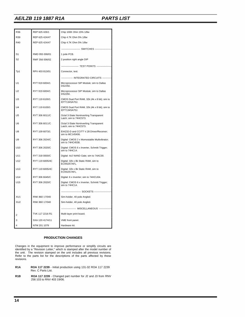
AE/LZB 119 1887 R1A PARTS LIST
14
R36 REP 625 426/1 Chip 100K Ohm 15% 1/8w
R39 REP 625 424/47 Chip 4.7K Ohm 5% 1/8w
R40 REP 625 424/47 Chip 4.7K Ohm 5% 1/8w
----------------------- SWITCHES ---------------------
S1 RMD 955 006/01 1 pole PCB.
S2 RΜF 356 006/02 2 position right angle DIP
--------------------- TEST POINTS -------------------
Tp1 RPV 403 813/01 Connector, test.
-------------- INTEGRATED CIRCUITS ------------
U1 RYT 919 6004/1 Microprocessor SIP Module; sim to DallasDS2250.
U2 RYT 919 6004/1 Microprocessor SIP Module; sim to DallasDS2250.
U3 RYT 119 6100/1 CMOS Dual Port RAM, 32k (4k x 8 bit); sim toIDT7134SA70J.
U4 RYT 119 6100/1 CMOS Dual Port RAM, 32k (4k x 8 bit); sim toIDT7134SA70J.
U5 RYT 306 6011/C Octal 3-State Noninverting TransparentLatch; sim to 74HC573.
U6 RYT 306 6011/C Octal 3-State Noninverting TransparentLatch; sim to 74HC573.
U8 RYT 109 6073/1 EIA232-D and CCITT V.28 Driver/Receiver;sim to MC145406.
U9 RYT 306 2024/C Digital: CMOS 2 x Momostable Multivibrator;sim to 74HC4538.
U10 RYT 306 2020/C Digital: CMOS 6 x Inverter, Schmitt Trigger;sim to 74HC14.
U11 RYT 318 0000/C Digital: 4x2 NAND Gate; sim to 74AC00.
U12 RYT 119 6005/4C Digital: 32k x 8k Static RAM, sim toECI55257AFL.
U13 RYT 119 6005/4C Digital: 32k x 8k Static RAM, sim toECI55257AFL.
U14 RYT 306 6045/C Digital: 6 x Inverter; sim to 74HCU04.
U15 RYT 306 2020/C Digital: CMOS 6 x Inverter, Schmitt Trigger;sim to 74HC14.
------------------------ SOCKETS ----------------------
XU1 RNK 860 17/040 Sim-holder, 40 pole Angled.
XU2 RNK 860 17/040 Sim-holder, 40 pole Angled.
------------------ MISCELLANEOUS ----------------
2 TVK 117 2216 R1 Multi-layer print board.
3 SXA 120 4174/11 VME front panel.
4 NTM 201 1079 Hardware kit.
PRODUCTION CHANGES
Changes in the equipment to improve performance or simplify circuits areidentified by a "Revision Letter," which is stamped after the model number ofthe unit. The revision stamped on the unit includes all previous revisions.Refer to the parts list for the descriptions of the parts affected by theserevisions.
R1A ROA 117 2239 - Initial production using 131-32 ROA 117 2239Rev. C Parts List.
R1B ROA 117 2239 - Changed part number for J2 and J3 from RNV256 103 to RNV 403 19/06.

IC DATA AE/LZB 119 1887 R1A
15
U1, U2 - MICROCONTROLLERRYT 919 6004/1 (DS2250)
U3, U4 - DUAL PORT RAMRYT 119 6100/1 (IDT7134SA70J)
U5, U6 - 8X1 D LATCHRYT 306 6011/C (74HC573)
8
7
6
5
1
2
3
4
VDD
DSCH
THRES
CONT
GND
TRIG
OUT
RESET
VDD
R
(8)
THRESHOLD
(6)
R
GND(1)
TRIGGER
(2)
CONTROL
(5)
RESET
(4)
R1
R
S
1
DISCHARGE
(7)
OUTPUT
(3)
hCAUTION
OBSERVE PRECAUTIONSFOR HANDLING
ELECTROSTATICSENSITIVEDEVICES
hCAUTION
OBSERVE PRECAUTIONSFOR HANDLING
ELECTROSTATICSENSITIVEDEVICES

AE/LZB 119 1887 R1A IC DATA
16
U8 - MONOLITHIC TIMERRYT 109 6073/1 (MC 145406)
U10, U15- 6 X INVERTER, SCHMITTTRIGGER RYT 306 2020/C (74HC14)
152 R
161
143 D
134 R
125 D
116 R
107 D
98 GND
DI3
DO3
DI2
DO2
DI1
DO1
VCC
VSS
Tx3
Rx3
Tx2
Rx2
Tx1
Rx1
VDDD = DriverR = ReceiverDI = Data InDO = Data Out
1 2
3 4
10 11
13 12
1
2
3
4
5
6
7GND
14
13
12
11
10
9
8
5 6
9 8
6Y
5A
5Y
4A
4Y
6A1Y
2A
2Y
3A
3Y
1A Vcc
U9 - 2 X CMOS MONOSTABLE MULTI-VIBRATORRYT 306 2024/C (74HC438)
1
2
3
4
5
6
7
16
15
14
13
12
11
10
FUNCTION TABLE
INPUTS OUTPUTS
Reset - Trigg+Triggr Q Q
L
H
HX
H
L
X = H or L
= from L to H
Vcc
R
RESET A
Tr A+
Tr A-
QA
QA
X
L
H
HL
8 9GND
A
C A
R
RESET B
Tr B+
Tr B-
QB
QB
B
C B
X
X
X
X HL
HL
= from H to L

IC DATA AE/LZB 119 1887 R1A
17
U11 - 4X2 NAND GATERYT 318 0000/C (74AC00)
U14- 6 X INVERTER, SCHMITT TRIGGERRYT 306 6045/C (74HCU04)
12
3
45
6
910
8
1213
11
1
2
3
4
5
6
7(GND)
14
13
12
11
10
9
8
(Vcc)
TRUTH TABLEINPUTS OUTPUTS
A1 (A2,A3,A4) B1 (B2,B3,B4) O1 (O2,O3,O4)
L L HL H HH L HH H L
1 2
3 4
10 11
13 12
1
2
3
4
5
6
7GND
14
13
12
11
10
9
8
5 6
9 8
6Y
5A
5Y
4A
4Y
6A1Y
2A
2Y
3A
3Y
1A Vcc
AE/LZB 119 1887 R1A IC DATA
18
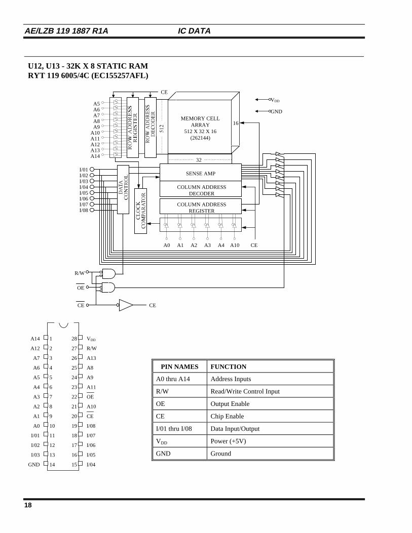
U12, U13 - 32K X 8 STATIC RAMRYT 119 6005/4C (EC155257AFL)
MEMORY CELLARRAY
512 X 32 X 16(262144)
A5A6A7A8A9
A10A11A12A13A14
32
SENSE AMP
COLUMN ADDRESSDECODER
COLUMN ADDRESSREGISTER
A0 A1 A2 A3 A10A4 CE
16
I/01I/02I/03I/04I/05I/06I/07I/08
CE
VDD
GND
R/W
OE
CE CE
A14
A12
A7
A6
A5
A4
A3
A2
A1
A0
I/01
I/02
I/03
GND
1
2
3
4
5
6
7
8
9
10
11
12
13
14
28
27
26
25
24
23
22
21
20
19
18
17
16
15
VDD
R/W
A13
A8
A9
A11
A10
I/08
I/07
I/06
I/05
I/04
CE
OE
PIN NAMES FUNCTION
A0 thru A14 Address Inputs
R/W Read/Write Control Input
OE Output Enable
CE Chip Enable
I/01 thru I/08 Data Input/Output
VDD Power (+5V)
GND Ground

OUTLINE DIAGRAM AE/LZB 119 1887 R1A
19
VERTICAL TURBO CARDROA 117 2239
(1078-ROA 117 2239, Sh. 1, Rev. A)

AE/LZB 119 1887 R1A
20
This page intentionally left blank

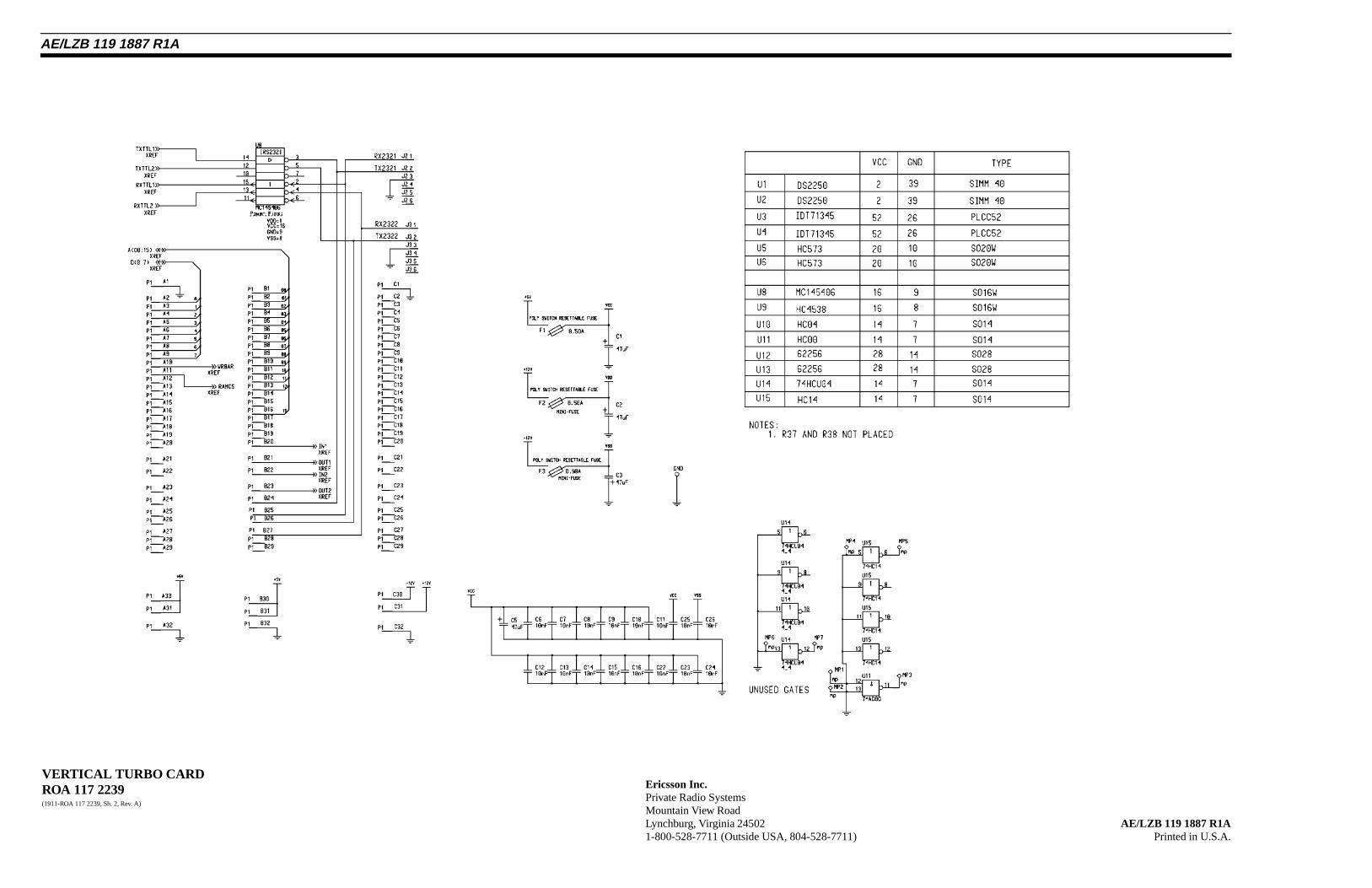
SCHEMATIC DIAGRAM
VERTICAL TURBO CARDROA 117 2239
(1911-ROA 117 2239, Sh. 1, Rev. A)
AE/LZB 119 1887 R1A
21
VERTICAL TURBO CARDROA 117 2239(1911-ROA 117 2239, Sh. 2, Rev. A)
Ericsson Inc.Private Radio SystemsMountain View RoadLynchburg, Virginia 24502 AE/LZB 119 1887 R1A1-800-528-7711 (Outside USA, 804-528-7711) Printed in U.S.A.
AE/LZB 119 1887 R1A