ee 466/586 vlsi design - washington...
TRANSCRIPT
Lecture 19 Implementation Methods (Cont’d)
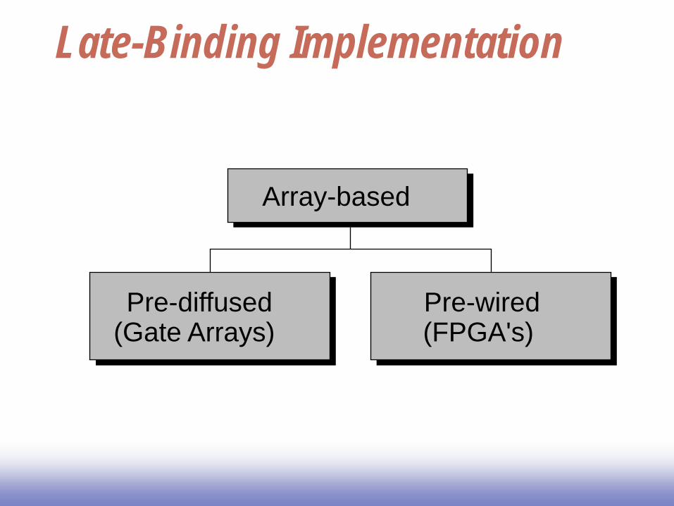
Pre-diffused (Gate Arrays)
Pre-wired (FPGA's)
Array-based
Late-Binding Implementation
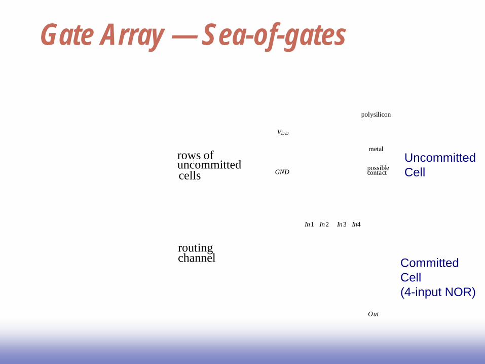
Gate Array — Sea-of-gates
rows of
cells
routing channel
uncommitted
VD D
GND
polysilicon
metal
possiblecontact
In1 In2 In3 In4
Out
Uncommitted Cell
Committed Cell (4-input NOR)
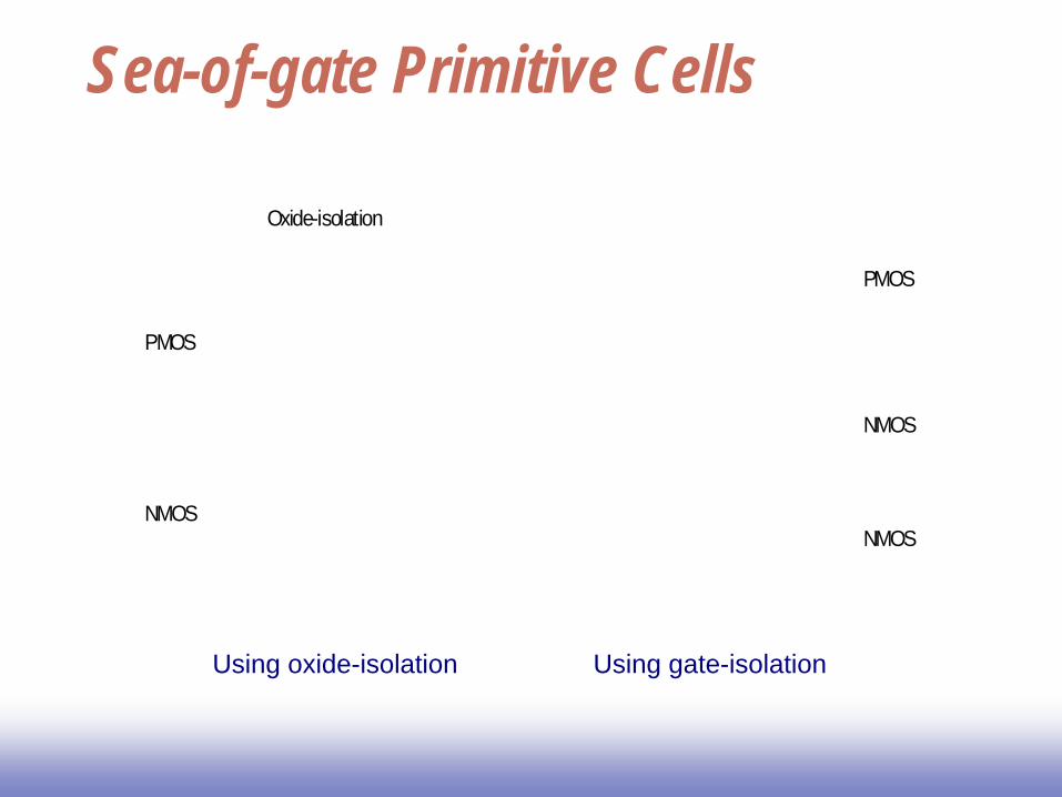
Sea-of-gate Primitive Cells
NMOS
PMOS
Oxide-isolation
PMOS
NMOS
NMOS
Using oxide-isolation Using gate-isolation
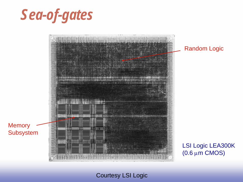
Sea-of-gates
Random Logic
Memory Subsystem
LSI Logic LEA300K (0.6 µm CMOS)
Courtesy LSI Logic
Prewired Arrays Classification of prewired arrays (or field-
programmable devices): Based on Programming Technique
Fuse-based (program-once) Non-volatile EPROM based RAM based
Programmable Logic Style Array-Based Look-up Table
Programmable Interconnect Style Channel-routing Mesh networks
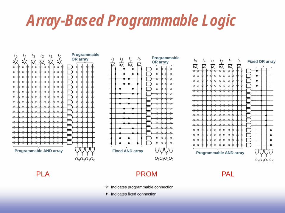
Array-Based Programmable Logic
PLA PROM PAL
I 5 I 4
O 0
I 3 I 2 I 1 I 0
O 1 O 2 O 3
Programmable AND array
Programmable OR array I 5 I 4
O 0
I 3 I 2 I 1 I 0
O 1 O 2 O 3
Programmable AND array
Fixed OR array
Indicates programmable connection
Indicates fixed connection
O 0
I 3 I 2 I 1 I 0
O 1 O 2 O 3
Fixed AND array
Programmable OR array
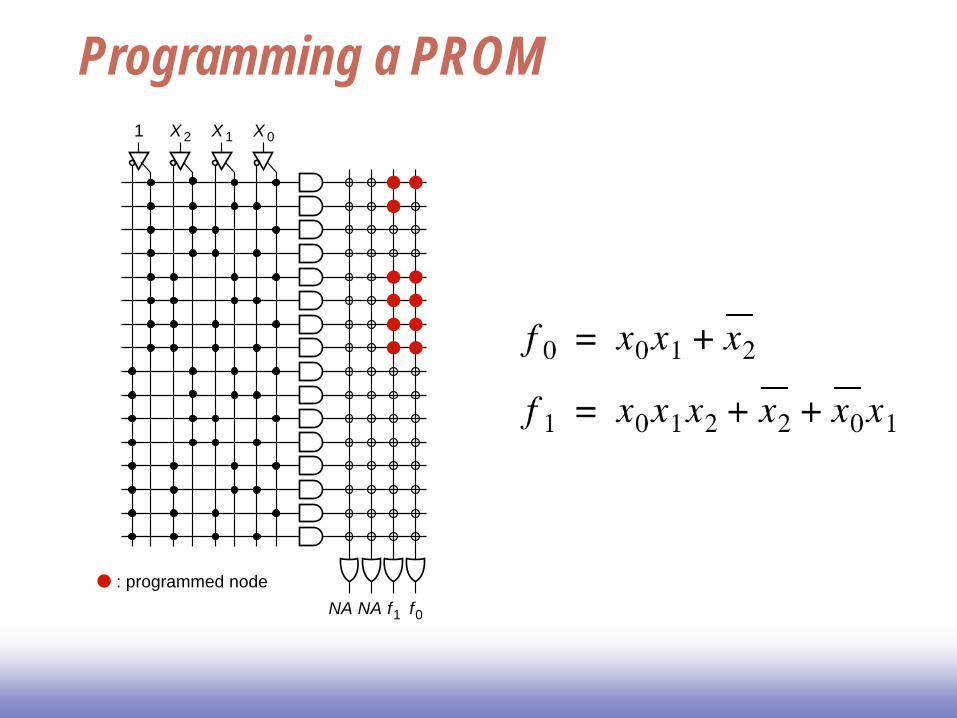
Programming a PROM
f 0
1 X 2 X 1 X 0
f 1 NA NA : programmed node
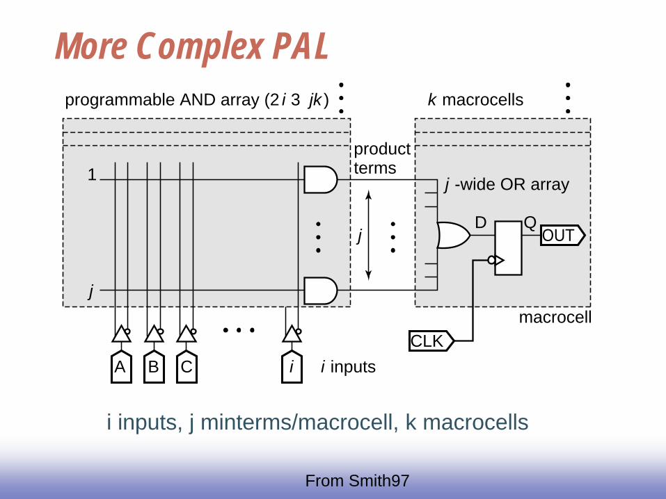
More Complex PAL
From Smith97
programmable AND array (2 i 3 jk ) k macrocells
j -wide OR array
j
macrocell
productterms
D Q
A
1
j
BCLK
OUT
C i i inputs
i inputs, j minterms/macrocell, k macrocells
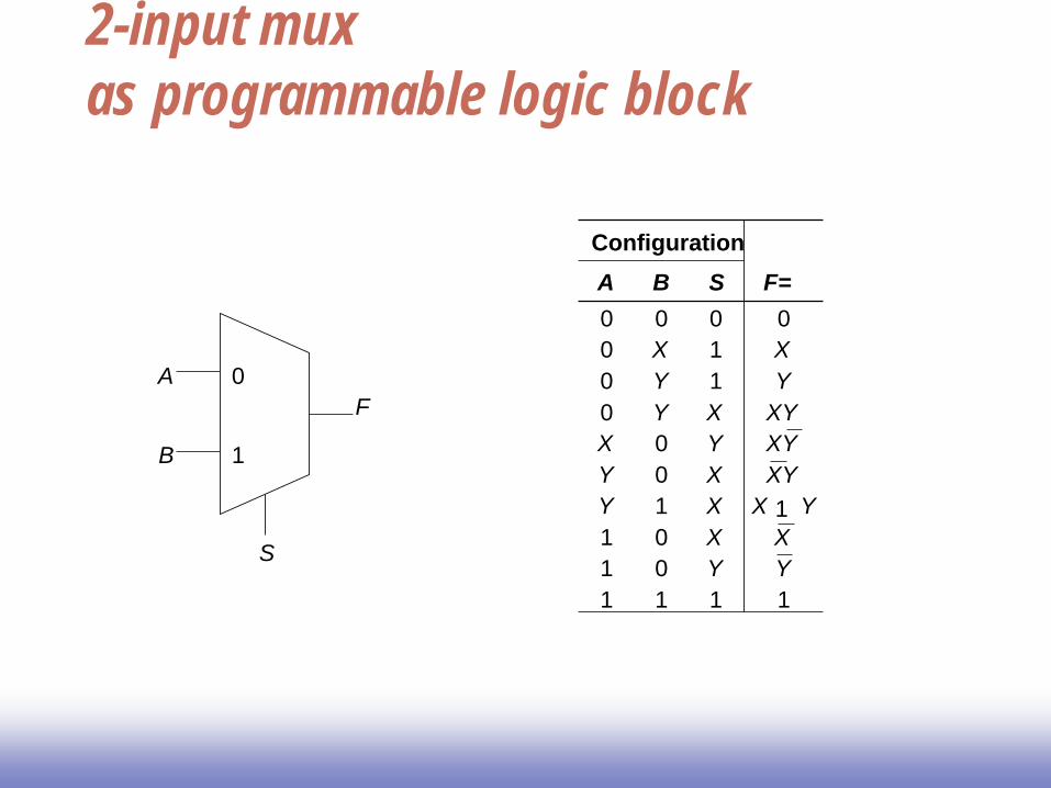
2-input mux as programmable logic block
F A 0
B
S
1
Configuration
A B S F= 0 0 0 0 0 X 1 X 0 Y 1 Y 0 Y X XY X 0 Y Y 0 X Y 1 X X 1 Y 1 0 X 1 0 Y 1 1 1 1
XY XY
X Y

Logic Cell of Actel Fuse-Based FPGA
A
B
SA Y
1
C
D
SB
1
S0S1
1
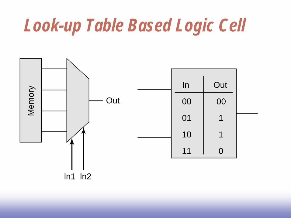
Look-up Table Based Logic Cell
Out
ln1 ln2
Mem
ory In Out
00 00
01 1
10 1
11 0
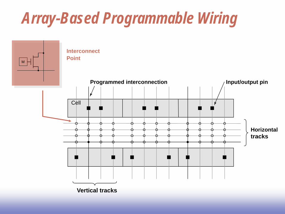
Array-Based Programmable Wiring
Input/output pin Programmed interconnection
Interconnect Point
Horizontal tracks
Vertical tracks
Cell
M
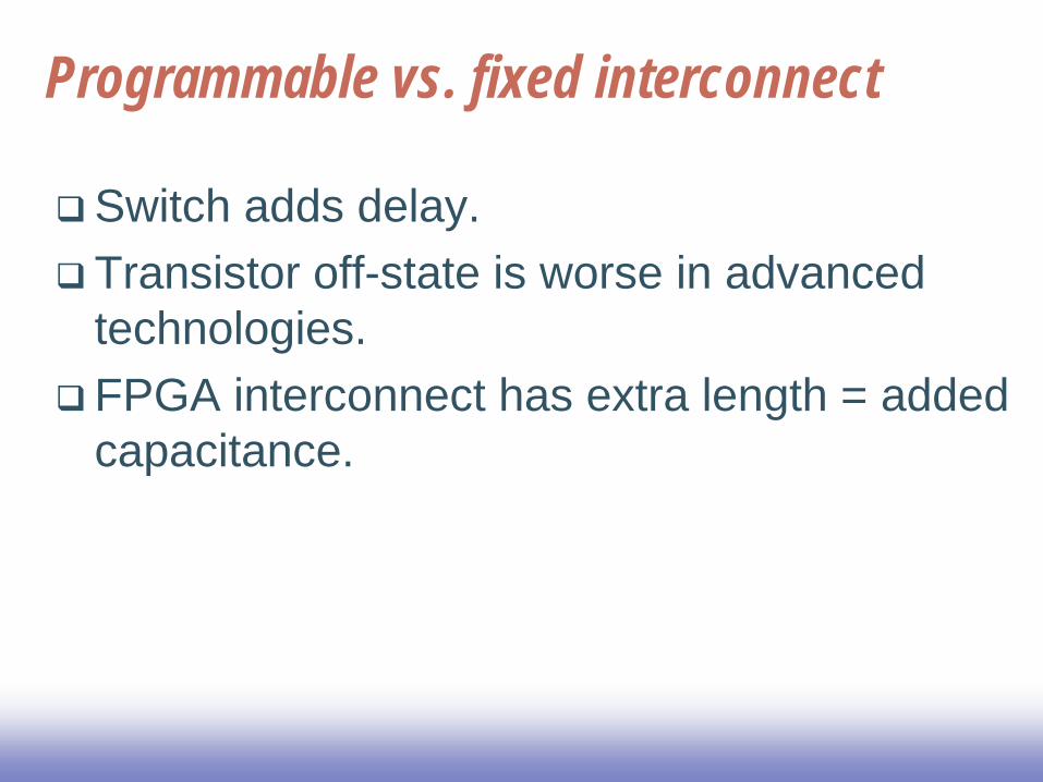
Programmable vs. fixed interconnect
Switch adds delay. Transistor off-state is worse in advanced
technologies. FPGA interconnect has extra length = added
capacitance.
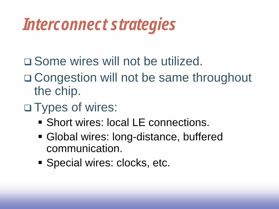
Interconnect strategies
Some wires will not be utilized. Congestion will not be same throughout
the chip. Types of wires: Short wires: local LE connections. Global wires: long-distance, buffered
communication. Special wires: clocks, etc.
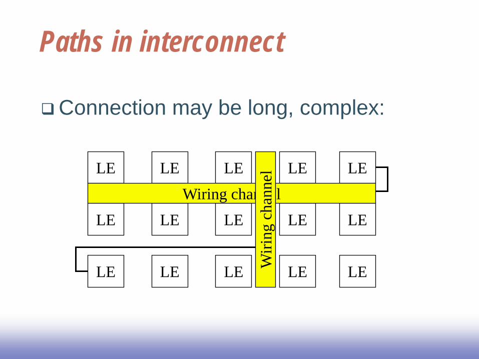
Paths in interconnect
Connection may be long, complex:
LE LE LE LE LE
LE LE LE LE LE
LE LE LE LE LE
Wiring channel
Wiri
ng c
hann
el
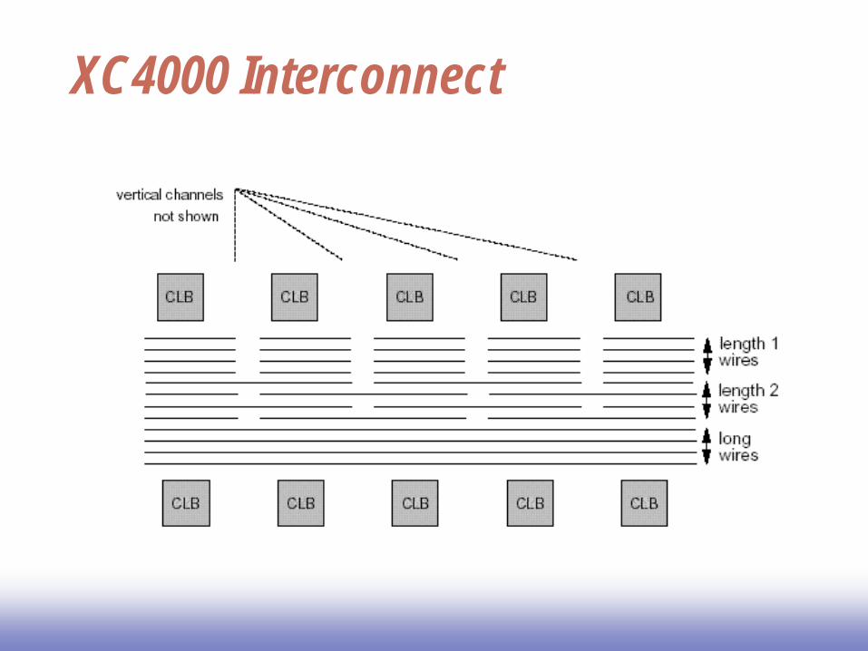
XC4000 Interconnect
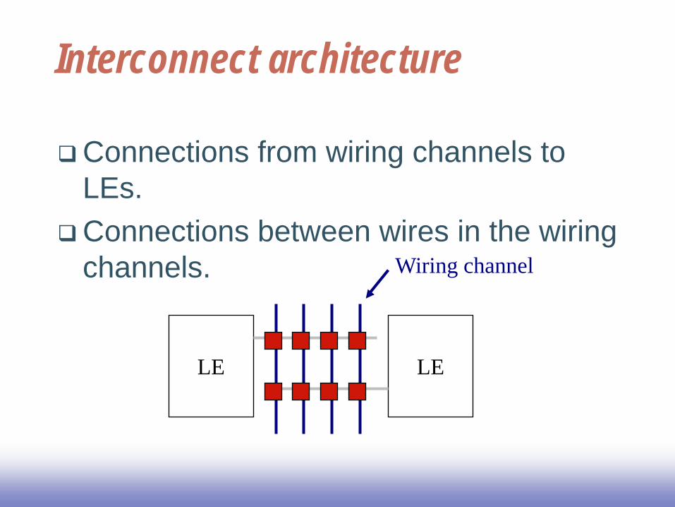
Interconnect architecture
Connections from wiring channels to LEs.
Connections between wires in the wiring channels.
LE LE
Wiring channel
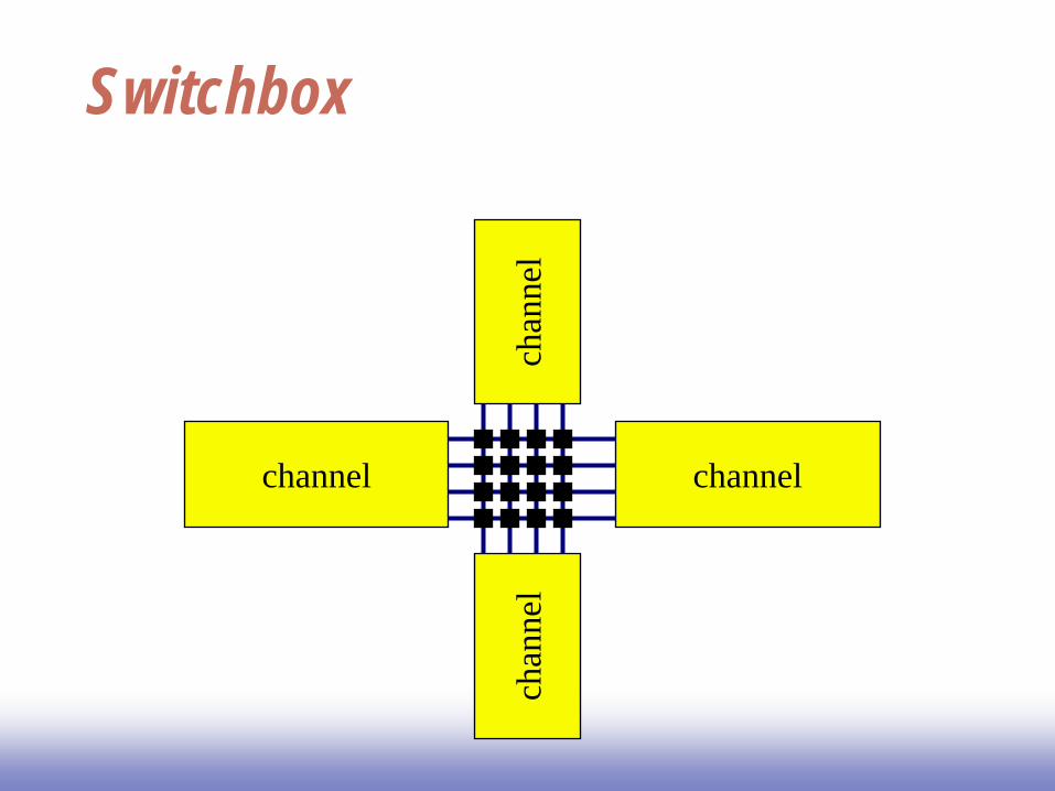
Switchbox
channel channel ch
anne
l ch
anne
l
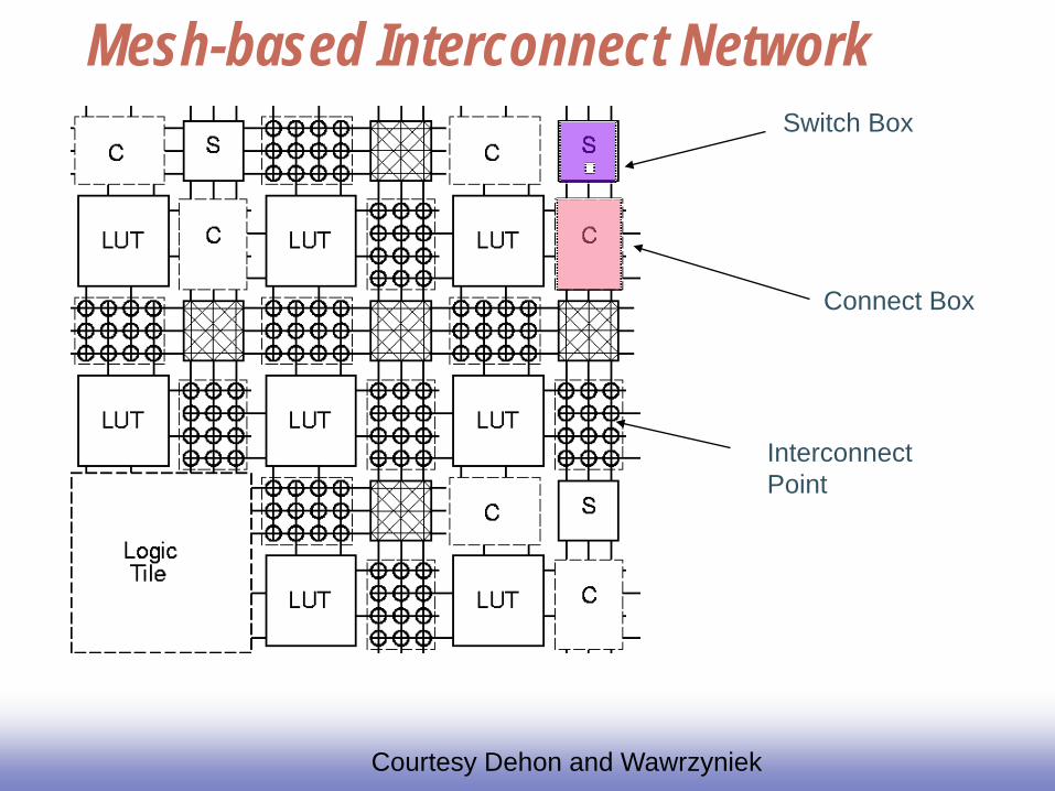
Mesh-based Interconnect Network Switch Box
Connect Box
Interconnect Point
Courtesy Dehon and Wawrzyniek
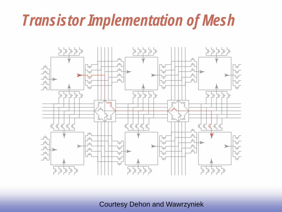
Transistor Implementation of Mesh
Courtesy Dehon and Wawrzyniek
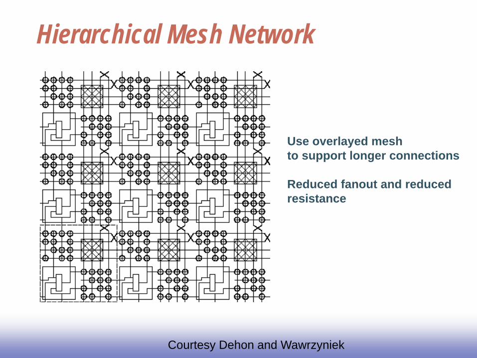
Hierarchical Mesh Network
Use overlayed mesh to support longer connections Reduced fanout and reduced resistance
Courtesy Dehon and Wawrzyniek
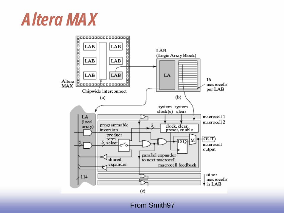
Altera MAX
From Smith97
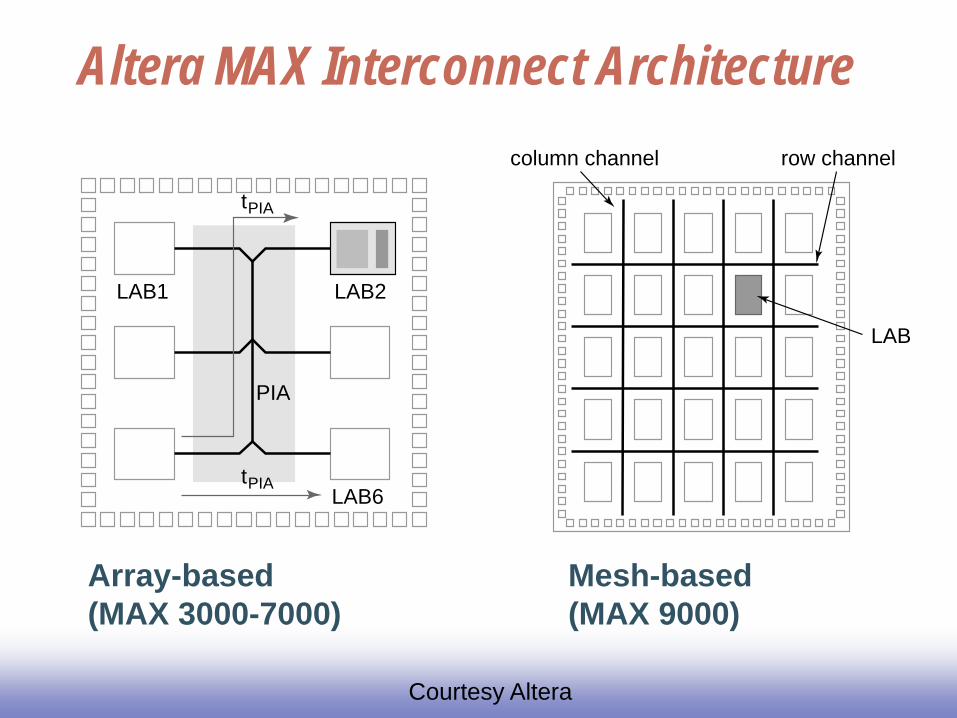
Altera MAX Interconnect Architecture
LAB2
PIA
LAB1
LAB6
t PIA
t PIA
row channel column channel
LAB
Courtesy Altera
Array-based (MAX 3000-7000)
Mesh-based (MAX 9000)
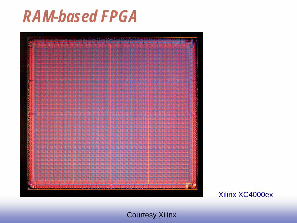
RAM-based FPGA
Xilinx XC4000ex
Courtesy Xilinx
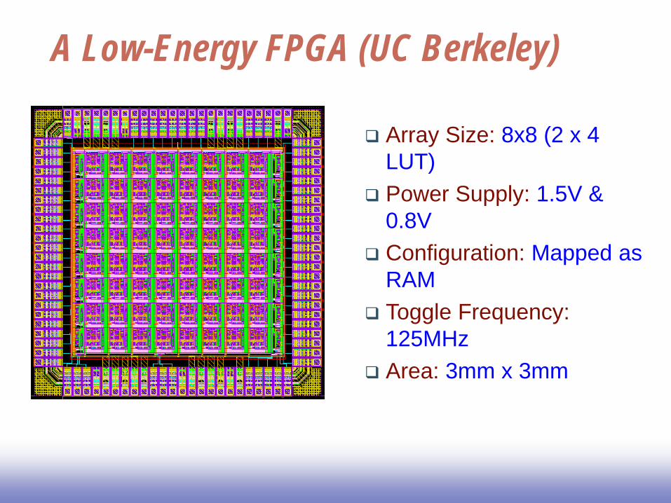
A Low-Energy FPGA (UC Berkeley)
Array Size: 8x8 (2 x 4 LUT)
Power Supply: 1.5V & 0.8V
Configuration: Mapped as RAM
Toggle Frequency: 125MHz
Area: 3mm x 3mm

Larger Granularity FPGAs
1-mm 2-metal CMOS tech
1.2 x 1.2 mm2
600k transistors
208-pin PGA
fclock = 50 MHz
Pav = 3.6 W @ 5V
Basic Module: Datapath
PADDI-2 (UC Berkeley)
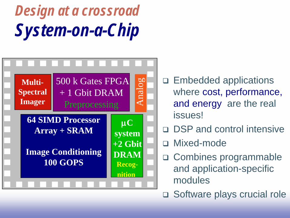
Design at a crossroad System-on-a-Chip
RAM
500 k Gates FPGA + 1 Gbit DRAM Preprocessing
Multi-
Spectral Imager
µC
system +2 Gbit DRAM Recog- nition
Ana
log
64 SIMD Processor Array + SRAM
Image Conditioning
100 GOPS
Embedded applications where cost, performance, and energy are the real issues!
DSP and control intensive Mixed-mode Combines programmable
and application-specific modules
Software plays crucial role
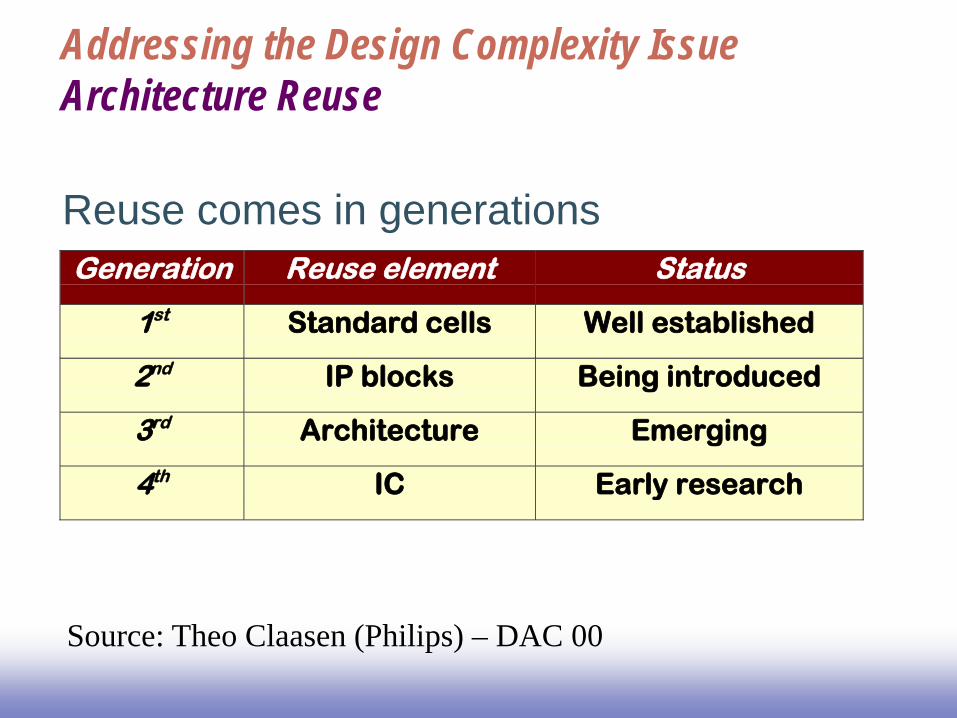
Addressing the Design Complexity Issue Architecture Reuse
Reuse comes in generations Generation Reuse element Status
1st Standard cells Well established
2nd IP blocks Being introduced
3rd Architecture Emerging
4th IC Early research
Source: Theo Claasen (Philips) – DAC 00
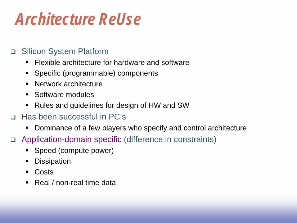
Architecture ReUse Silicon System Platform
Flexible architecture for hardware and software Specific (programmable) components Network architecture Software modules Rules and guidelines for design of HW and SW
Has been successful in PC’s Dominance of a few players who specify and control architecture
Application-domain specific (difference in constraints) Speed (compute power) Dissipation Costs Real / non-real time data
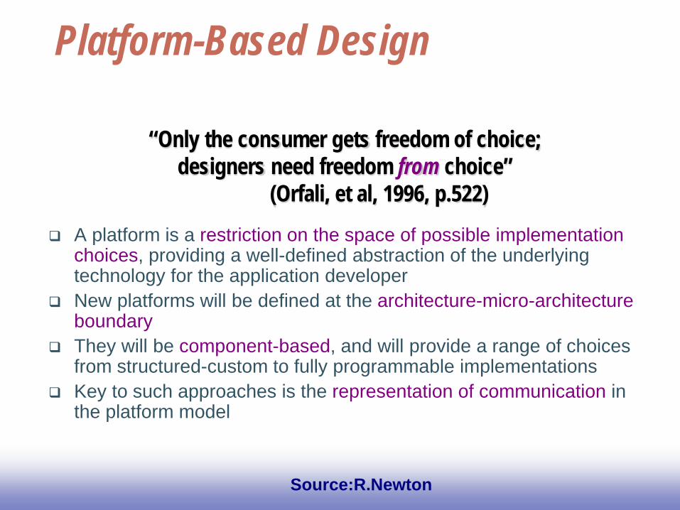
Platform-Based Design
A platform is a restriction on the space of possible implementation choices, providing a well-defined abstraction of the underlying technology for the application developer
New platforms will be defined at the architecture-micro-architecture boundary
They will be component-based, and will provide a range of choices from structured-custom to fully programmable implementations
Key to such approaches is the representation of communication in the platform model
“Only the consumer gets freedom of choice; designers need freedom from choice”
(Orfali, et al, 1996, p.522)
Source:R.Newton
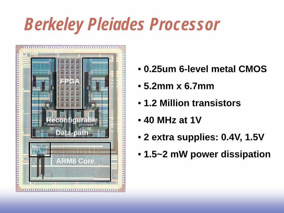
Berkeley Pleiades Processor
• 0.25um 6-level metal CMOS
• 5.2mm x 6.7mm
• 1.2 Million transistors
• 40 MHz at 1V
• 2 extra supplies: 0.4V, 1.5V
• 1.5~2 mW power dissipation Interface
Reconfigurable
Data-path
FPGA
ARM8 Core
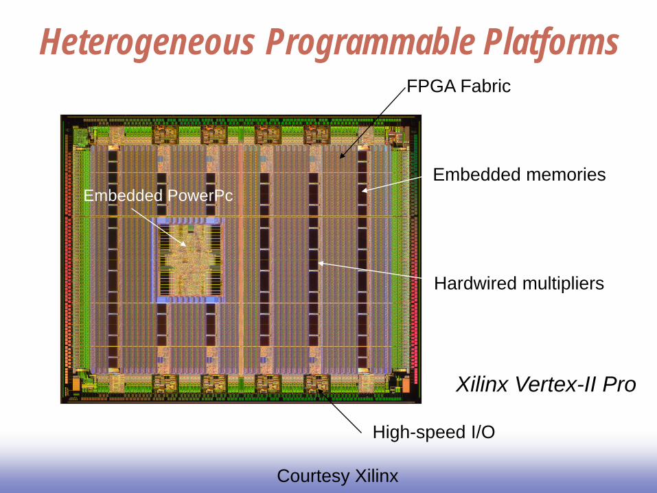
Heterogeneous Programmable Platforms
Xilinx Vertex-II Pro
Courtesy Xilinx
High-speed I/O
Embedded PowerPc Embedded memories
Hardwired multipliers
FPGA Fabric
Summary
Digital CMOS Design is kicking and healthy Some major challenges down the road
caused by Deep Sub-micron Super GHz design Power consumption!!!! Reliability – making it work Some new circuit solutions are bound to emerge
Who can afford design in the years to come? Some major design methodology change in the making!