ee141 system-on-chip test architectures ch. 2 – digital test architectures - p. 1 chapter 2...
Post on 19-Dec-2015
223 views
TRANSCRIPT
EE141System-on-Chip Test Architectures Ch. 2 – Digital Test Architectures - P. 1
Chapter 2Chapter 2
Digital Test ArchitecturesDigital Test Architectures

EE141System-on-Chip Test Architectures Ch. 2 – Digital Test Architectures - P. 2
What is this chapter about?What is this chapter about? Introduce Basic Design for Testability
(DFT) Techniques
Focus on Widely Used or Emerging DFT Architectures
Illustrate Basic Test Architectures, Low-Power Test Architectures, and At-Speed Test Architectures
EE141System-on-Chip Test Architectures Ch. 2 – Digital Test Architectures - P. 3
Digital Test ArchitecturesDigital Test Architectures
IntroductionScan DesignLogic Built-In Self-TestTest CompressionRandom-Access Scan DesignConcluding Remarks

EE141System-on-Chip Test Architectures Ch. 2 – Digital Test Architectures - P. 4
IntroductionIntroduction
HelloEvolution of DFT advances in testing digital circuits
Scan LogicBIST
At-SpeedDelay
Testing
TestCompre-
ssion
Low-PowerTesting
Fault ToleranceDefect andTolerance

EE141System-on-Chip Test Architectures Ch. 2 – Digital Test Architectures - P. 5
IntroductionIntroduction Scan Design
Replace all selected storage elements with scan cells Connect scan cells into multiple shift registers (scan chains) Become inefficient to test deep submicron or nanometer
VLSI
Logic Built-In Self-Test (BIST) Combine with scan approach at the design stage Generate test patterns and analyze the output response Crucial for safety-critical and mission-critical applications

EE141System-on-Chip Test Architectures Ch. 2 – Digital Test Architectures - P. 6
IntroductionIntroduction Test Compression
A supplemental DFT technique to scan Can reduce test data volume and test application time Add some additional on-chip hardware
Random-Access Scan Design Randomly and uniquely addressable, similar to RAM A promising alternative to Scan design for shift power
reduction

EE141System-on-Chip Test Architectures Ch. 2 – Digital Test Architectures - P. 7
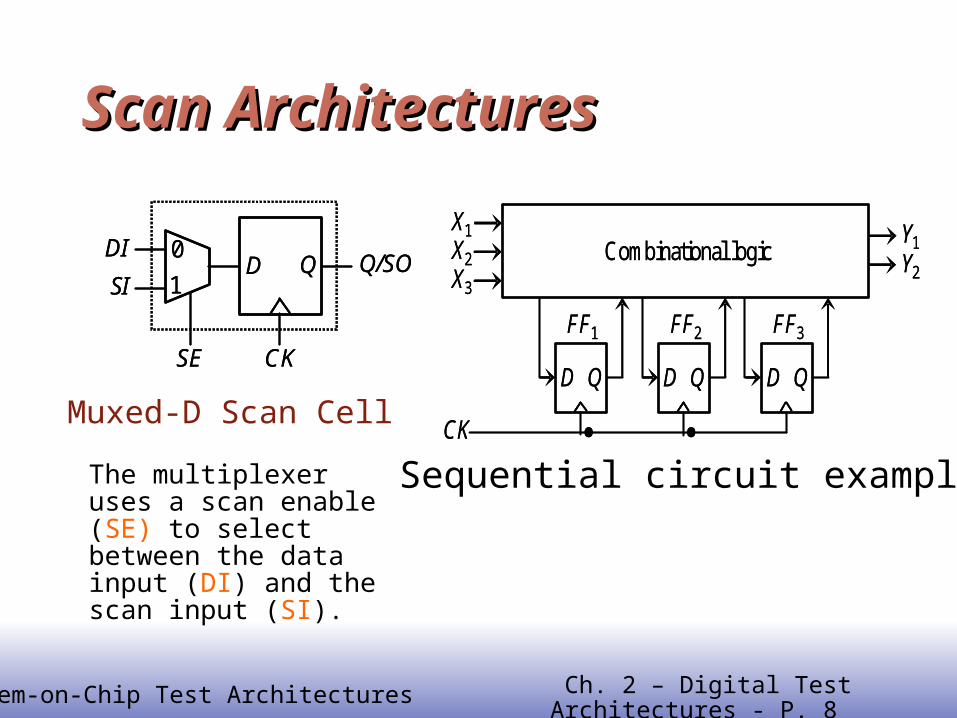
Scan DesignScan Design Widely used structured DFT architecture Replace all selected storage elements with scan cells Connect scan cells into scan chains Operated in three modes:
Normal mode– All test signals are turned off.– The scan design operates in the circuit’s original functional
configuration. Shift mode
– to shift data into and out of the scan cells Capture mode
– to capture test response into scan cells
EE141System-on-Chip Test Architectures Ch. 2 – Digital Test Architectures - P. 8
Muxed-D Scan Cell
The multiplexer uses a scan enable (SE) to select between the data input (DI) and the scan input (SI).
Sequential circuit example
Scan ArchitecturesScan Architectures
CK
D QDI
SI
0
1
SE
Q/SO
CK
D QDI
SI
0
1
SE
Q/SO
.D Q
FF1
CK
X2 Combinational logicX3
X1
Y2
Y1
D Q
FF2
D Q
FF3
..D Q
FF1
CK
X2 Combinational logicX3
X1
Y2
Y1
D Q
FF2
D Q
FF3
.
EE141System-on-Chip Test Architectures Ch. 2 – Digital Test Architectures - P. 9
Scan ArchitecturesScan Architectures
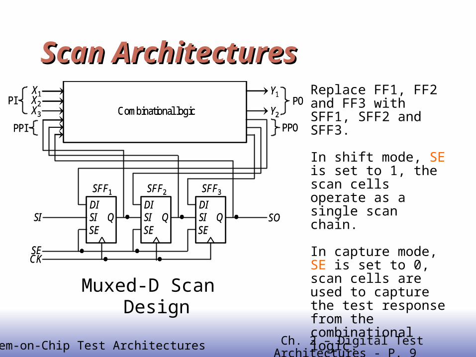
Muxed-D Scan Design
Replace FF1, FF2 and FF3 with SFF1, SFF2 and SFF3.
In shift mode, SE is set to 1, the scan cells operate as a single scan chain.
In capture mode, SE is set to 0, scan cells are used to capture the test response from the combinational logic. .
X2Combinational logicX3
X1
Y2
Y1PI
PPI
PO
PPO
DIQ
SFF1
SISE
.
DIQ
SFF2
SISE
SE
DIQ
SFF3
SISE
CK
SI
. .
... SO
.
X2Combinational logicX3
X1
Y2
Y1PI
PPI
PO
PPO
DIQ
SFF1
SISE
.
DIQ
SFF2
SISE
SE
DIQ
SFF3
SISE
CK
SI
. .
... SO

EE141System-on-Chip Test Architectures Ch. 2 – Digital Test Architectures - P. 10
Clocked-Scan Cell
Input selection is conducted using two independent clocks, data clock DCK and shift clock SCK.
Scan ArchitecturesScan Architectures
SCK
Q/SODI
SI
DCK SCK
Q/SODI
SI
DCK
EE141System-on-Chip Test Architectures Ch. 2 – Digital Test Architectures - P. 11
Scan ArchitecturesScan Architectures
Clocked-Scan Design
DCK and SCK are used for distinguishing shift and capture operations; while SE is used to switch the shift and capture operations in muxed-D scan design.
.. .
X2Combinational logicX3
X1
Y2
Y1PI
PPI
PO
PPO
SFF1
.
SFF2
DCKSCK
SI ... SODI
QSIDCK SCK
DIQSI
DCK SCK
DIQSI
DCK SCK
SFF3
.. .
X2Combinational logicX3
X1
Y2
Y1PI
PPI
PO
PPO
SFF1
.
SFF2
DCKSCK
SI ... SODI
QSIDCK SCK
DIQSI
DCK SCK
DIQSI
DCK SCK
DIQSI
DCK SCK
DIQSI
DCK SCK
DIQSI
DCK SCK
SFF3

EE141System-on-Chip Test Architectures Ch. 2 – Digital Test Architectures - P. 12
LSSD Scan Cell
Polarity–hold shift register latch (SRL)
SRL can be used as an LSSD scan cell. This scan cell contains two latches, a master two-port D latch L
1
and a slave D latch L2.
Clocks C, A, and B are used to select between D and +L
1
and +L2.
Level-Sensitive Scan Design (LSSD) can be implemented using a single-latch design or a double-latch design.
Scan ArchitecturesScan Architectures
+L2
C
D . ..
.
A
I .
..
.B
+L1
L1
L2
SRL
+L2
C
D . ..
.
A
I .
..
.B
+L1
L1
L2
SRL
EE141System-on-Chip Test Architectures Ch. 2 – Digital Test Architectures - P. 13
Scan ArchitecturesScan Architectures
LSSD single-latch design
The system clocks C
1 and C
2 should
be applied in a nonoverlapping fashion.
X2
Combinational logic 1X1
Y2
SOD
+L2
SRL1
IC
+L1AB
.
D+L2
SRL2
IC
+L1AB
D+L2
SRL3
IC
+L1AB
SI
C1AB
.. ..C2
Combinational logic 2X3
Y1X2
Combinational logic 1X1
Y2
SOD
+L2
SRL1
IC
+L1AB
.
D+L2
SRL2
IC
+L1AB
D+L2
SRL3
IC
+L1AB
SI
C1AB
.. ..C2
Combinational logic 2X3
Y1
EE141System-on-Chip Test Architectures Ch. 2 – Digital Test Architectures - P. 14
Scan ArchitecturesScan Architectures
LSSD double-latch design
During the shift operation, clocks A and B are applied in a nonoverlapping manner, and the scan cells, SRL1 ~ SRL3, form a single scan chain from SI to SO.
During the capture operation, clocks C
1and
C2are applied in a non-
overlapping manner to load thetest response from the combinational logic into the scan cells.
X2 Combinational logicX3
X1
Y2
Y1
SOD
+L2
SRL1
IC
+L1AB
.
D+L2
SRL2
IC
+L1AB
D+L2
SRL3
IC
+L1AB
SI
C1A
C2 or B..
...
. . .
X2 Combinational logicX3
X1
Y2
Y1
SOD
+L2
SRL1
IC
+L1AB
.
D+L2
SRL2
IC
+L1AB
D+L2
SRL3
IC
+L1AB
SI
C1A
C2 or B..
...
. . .

EE141System-on-Chip Test Architectures Ch. 2 – Digital Test Architectures - P. 15
Scan ArchitecturesScan Architectures Enhanced-Scan Design
An alternative at-speed scan design for testing delay faults; testing of a delay fault requires a pair of test vectors in an at-speed fashion.
Enhanced-scan cell can store two bits of data; achieved by adding a D latch to a muxed-D scan cell or clocked-scan cell.
Disadvantages:– Higher hardware overhead– May activate many false paths causing an over-test
problem

EE141System-on-Chip Test Architectures Ch. 2 – Digital Test Architectures - P. 16
Enhanced-Scan Design
The first test vector V1 is shifted into SFF1 ~ SFFs and then stored into the additional latches (LA1 ~ LAs) when the UPDATE signal is set to 1.
Next, the second test vector V2 is shifted into the scan cells while the UPDATE signal is set to 0, in order to preserve the V1 value in the latches (LA1 ~ LAs).
Once the second vector V2 is shifted in, the UPDATE signal is applied, in order to change V1 to V2 while capturing the output response at-speed into the scan cells by applying CK after exactly one clock cycle.
Scan ArchitecturesScan Architectures
LA1
D
C
.DIQSDI
.CK
SFF1
SISESE .
Q.UPDATE
LA2
D
C
.DIQ
.
SFF2
SISE
Q
.
...X2
Combinational logic
Xn
.
.
X1
. Y2
Ym
Y1
LAs
D
C
DIQ
SFFs
SISE
Q
.
…
…
……
LA1
D
C
.DIQSDI
.CK
SFF1
SISESE .
Q.UPDATE
LA2
D
C
.DIQ
.
SFF2
SISE
Q
.
...X2
Combinational logic
Xn
.
.
X1
. Y2
Ym
Y1
LAs
D
C
DIQ
SFFs
SISE
Q
.
…
…
……

EE141System-on-Chip Test Architectures Ch. 2 – Digital Test Architectures - P. 17
Low-Power Scan ArchitecturesLow-Power Scan Architectures
□
Serial Scan Design Advantage:
– Low routing overhead Disadvantages:
– Scan cells cannot be controlled or observed without affecting the values of other scan cells in the same scan chain
– High switching activities during shift and capture can cause excessive shift (or test) power dissipation
Low-Power Scan Design Test power is related to dynamic power, and is proportional
to VDD2f
– VDD is the supply voltage– f is the switching frequency of the circuit node under test
EE141System-on-Chip Test Architectures Ch. 2 – Digital Test Architectures - P. 18
Example Low-Power Scan ArchitecturesExample Low-Power Scan Architectures
□
Reduced-Voltage Low-Power Scan Design Reduce the supply voltage
Reduced-Frequency Low-Power Scan Design Slow down the shift clock frequency but increase test
application time Multi-Phase Low-Power Scan Design
Split the shift clock into a number of nonoverlapping clock phases but increase routing overhead and complexity during clock tree synthesis
Bandwidth-Matching Low-Power Scan Design Use pairs of serial-in/parallel-out shift register and parallel-
in/serial-out shift register for bandwidth matching Hybrid Low-Power Scan Design
Combine any of the above-mentioned low-power scan designs
EE141System-on-Chip Test Architectures Ch. 2 – Digital Test Architectures - P. 19
□
The clock CK is split into three clock phases CK
1,
CK2, and CK
3.
Using this scheme, a 3X reduction in shift power can be achieved, assuming each clock drives an equal number of scan cells.
Multi-Phase Low-Power Scan DesignMulti-Phase Low-Power Scan Design
X2Combinational logicX3
X1
Y2
Y1PI
PPI
PO
PPO
DIQ
SFF1
SISE
DIQ
SFF2
SISE
SE
DIQ
SFF3
SISE
CK1
SI
. .
... SO
CK2CK3
X2Combinational logicX3
X1
Y2
Y1PI
PPI
PO
PPO
DIQ
SFF1
SISE
DIQ
SFF2
SISE
SE
DIQ
SFF3
SISE
CK1
SI
. .
... SO
CK2CK3
EE141System-on-Chip Test Architectures Ch. 2 – Digital Test Architectures - P. 20
Bandwidth-Matching Low-Power Scan DesignBandwidth-Matching Low-Power Scan Design
□
Each scan chain is split into 4 sub-scan chains with the SI and SO ports of each 4 sub-scan chains connected to a serial-in/parallel-out shift register and a parallel-in/serial-out shift register, respectively.
TDDM
TDM
s10 s11 s12 s13
SI1 SIm
t10 t11 t12 t13
sm0 sm1 sm2 sm3
tm0 tm1 tm2 tm3
SO1 SOm
. . .
. . .
. . .
Full-ScanCircuit
ClockController
. . .
. . .
.ck1
ck2
TDDM
TDM
s10 s11 s12 s13
SI1 SIm
t10 t11 t12 t13
sm0 sm1 sm2 sm3
tm0 tm1 tm2 tm3
SO1 SOm
. . .
. . .
. . .
Full-ScanCircuit
ClockController
. . .
. . .
.ck1
ck2
EE141System-on-Chip Test Architectures Ch. 2 – Digital Test Architectures - P. 21
At-Speed Scan ArchitecturesAt-Speed Scan Architectures
□
Synchronous Design A scan design if the active edges of all
capture clocks controlling the clock domains can be aligned precisely or triggered simultaneously
Asynchronous Design A scan design if not synchronous

EE141System-on-Chip Test Architectures Ch. 2 – Digital Test Architectures - P. 22
At-Speed Scan ArchitecturesAt-Speed Scan Architectures Two basic schemes for test multiple clock domain at-speed
Skewed-load (Launch-on-shift)– Use the last shift clock pulse followed immediately by a capture
clock pulse to launch the transition and capture the output response
Double-capture (Launch-on-capture or Broad-side)– Use two consecutive capture clock pulses to launch the
transition and capture the output test response Similarity
Can test path-delay faults and transition faults. The second capture clock pulse must be running at the domain’s operating frequency or at-speed.
Difference Skewed-load requires the domain’s SE to switch value between the
launch and capture clock pulses making SE act as a clock signal.
EE141System-on-Chip Test Architectures Ch. 2 – Digital Test Architectures - P. 23
Basic At-Apeed Test SchemesBasic At-Apeed Test Schemes
Skewed-load Double-capture
Shift Shift Last Shift
Shift
SE
CK C
aptu
re
Lau
nch
Shift Shift Dead Cycles
Shift
SE
CK
Cap
ture
L
aunc
h
EE141System-on-Chip Test Architectures Ch. 2 – Digital Test Architectures - P. 24
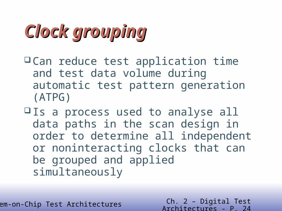
Clock groupingClock grouping
Can reduce test application time and test data volume during automatic test pattern generation (ATPG)
Is a process used to analyse all data paths in the scan design in order to determine all independent or noninteracting clocks that can be grouped and applied simultaneously
EE141System-on-Chip Test Architectures Ch. 2 – Digital Test Architectures - P. 25
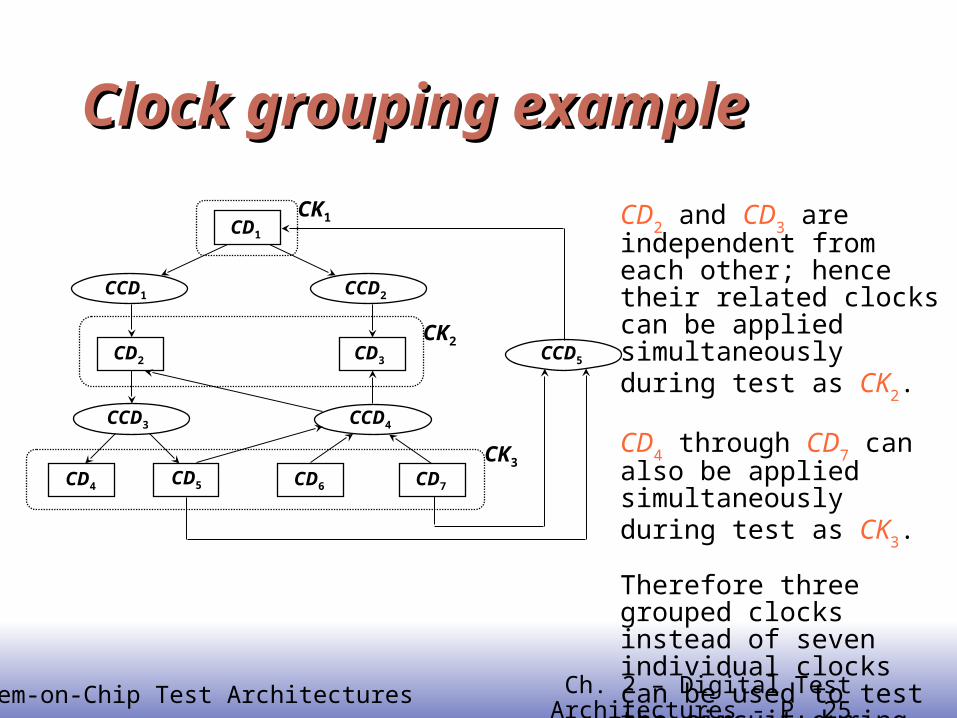
Clock grouping exampleClock grouping example
CD2 and CD
3 are independent
from each other; hence their related clocks can be applied simultaneously during test as CK
2.
CD
4 through CD
7 can also be
applied simultaneously during test as CK
3.
Therefore three grouped clocks instead of seven individual clocks can be used to test the circuit during the capture operation.
CD1
CCD2
CCD1
CD2 CD3
CD4 CD5 CD6 CD7
CCD3 CCD4
CCD5
CK1
CK2
CK3

EE141System-on-Chip Test Architectures Ch. 2 – Digital Test Architectures - P. 26
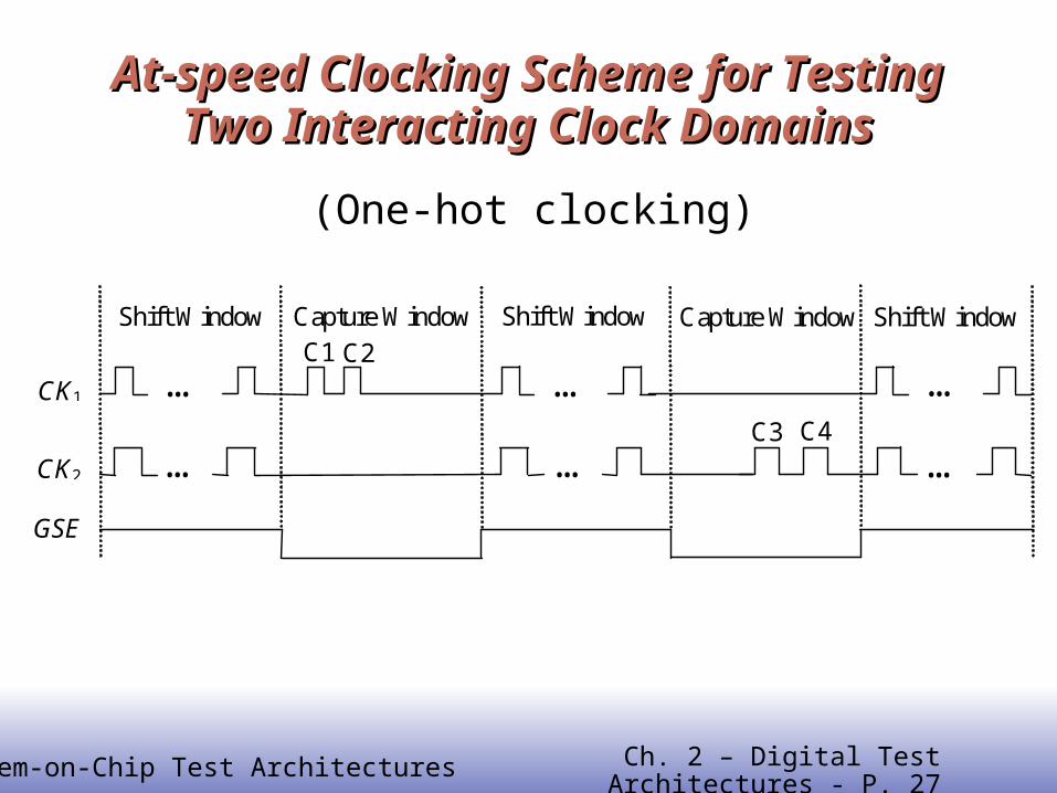
Clock schemesClock schemes One-hot clocking
Apply only one grouped clock during each capture operation Produce the highest fault coverage but generate most test
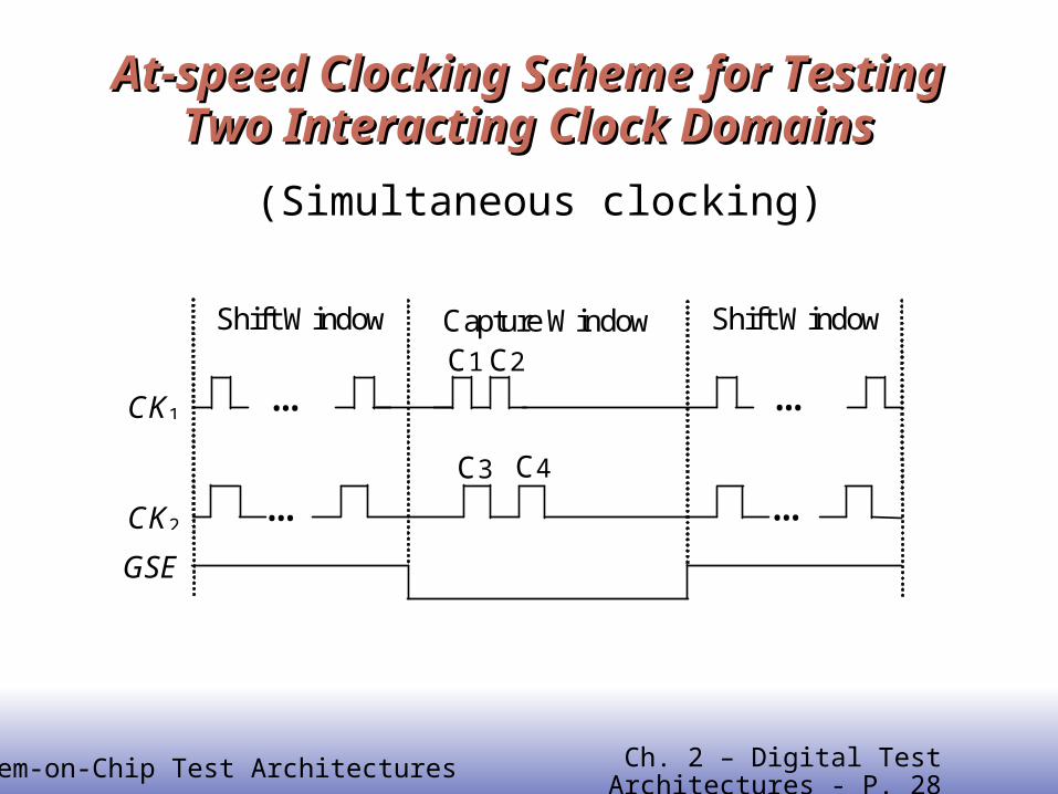
patterns Simultaneous clocking
Mask off unknown values at the originating scan cells or receiving scan cells across clock domains
Generate the least number of patterns but may result in high fault coverage loss
Staggered clocking Grouped clocks are applied sequentially Generate pattern count close to simultaneous clocking and
fault coverage close to one-hot clocking
EE141System-on-Chip Test Architectures Ch. 2 – Digital Test Architectures - P. 27
At-speed Clocking Scheme for Testing Two At-speed Clocking Scheme for Testing Two Interacting Clock DomainsInteracting Clock Domains
(One-hot clocking)
Shift Window Capture Window Shift Window Capture Window Shift Window
CK1 … … … C1 C2
CK2 … C4
… … C3
GSE
EE141System-on-Chip Test Architectures Ch. 2 – Digital Test Architectures - P. 28
At-speed Clocking Scheme for Testing Two At-speed Clocking Scheme for Testing Two Interacting Clock DomainsInteracting Clock Domains
(Simultaneous clocking)
Shift Window Capture Window Shift Window
…
…
…
…
CK1
CK2
C1 C2
C3 C4
GSE
EE141System-on-Chip Test Architectures Ch. 2 – Digital Test Architectures - P. 29
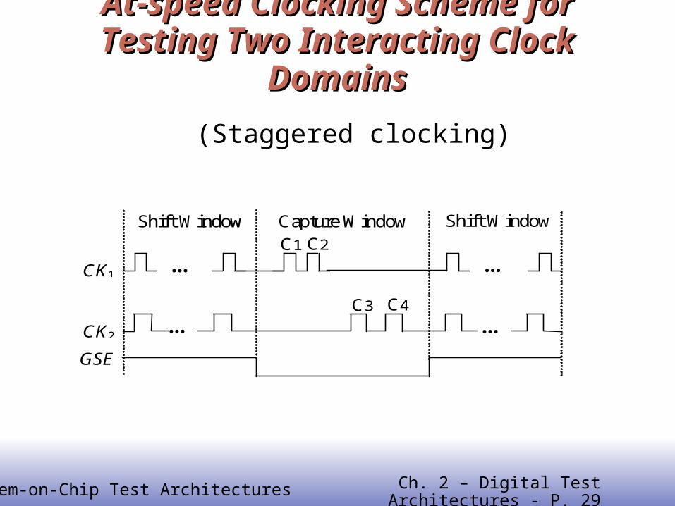
At-speed Clocking Scheme for Testing At-speed Clocking Scheme for Testing Two Interacting Clock DomainsTwo Interacting Clock Domains
(Staggered clocking)
Shift Window Capture Window Shift Window
…
…
…
…
CK1
CK2
C1 C2
C3 C4
GSE

EE141System-on-Chip Test Architectures Ch. 2 – Digital Test Architectures - P. 30
How to Generate Shift and Capture ClocksHow to Generate Shift and Capture Clocks
Supplied from the Tester Increase test cost Limited high-frequency channels
Generated by Phase-Locked Loop (PLL) Pipelined Scan Enable (SE) signal Test clock controller

EE141System-on-Chip Test Architectures Ch. 2 – Digital Test Architectures - P. 31
Pipelined Scan Enable (SE) Pipelined Scan Enable (SE) DesignDesign
CK
D Q D Q
D Q CK CK
SE
CK
SE1 for positive-edge scan cells
SE2 for negative-edge scan cells

EE141System-on-Chip Test Architectures Ch. 2 – Digital Test Architectures - P. 32
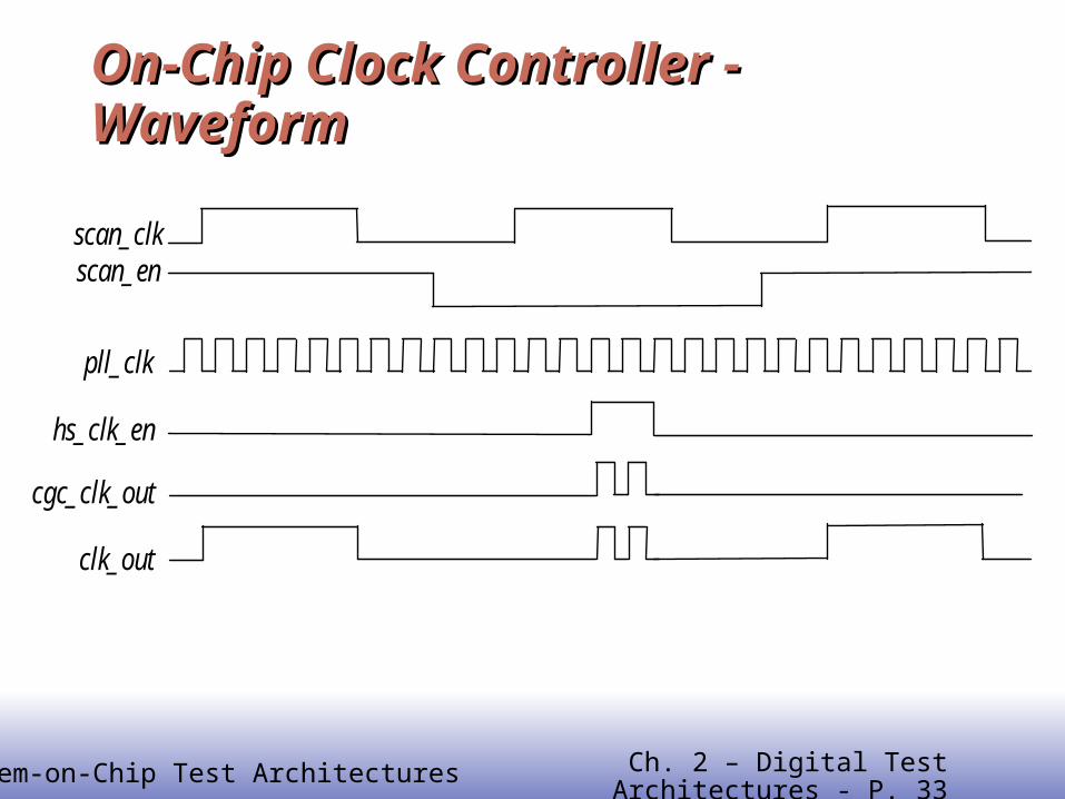
On-Chip Clock ControllerOn-Chip Clock Controller
When scan_en is set to 1, scan_clk is directly connected to clk_out; when scan_en is set to 0, the output of the clock-gating cell is directly connected to clk_out.
The clock-gating cell makes sure that no glitches or spikes appear on clk_out.
Q1 Q2 Q3 Q5 Q4
Shift Register
clk_out
hs_clk_en
cgc_clk_out
scan_en
scan_clk
pll_clk PLL
Clock-Gating Cell 0
1
D Q
EE141System-on-Chip Test Architectures Ch. 2 – Digital Test Architectures - P. 33
On-Chip Clock Controller - WaveformOn-Chip Clock Controller - Waveform
scan_clk scan_en
pll_clk
hs_clk_en
cgc_clk_out
clk_out
EE141System-on-Chip Test Architectures Ch. 2 – Digital Test Architectures - P. 34
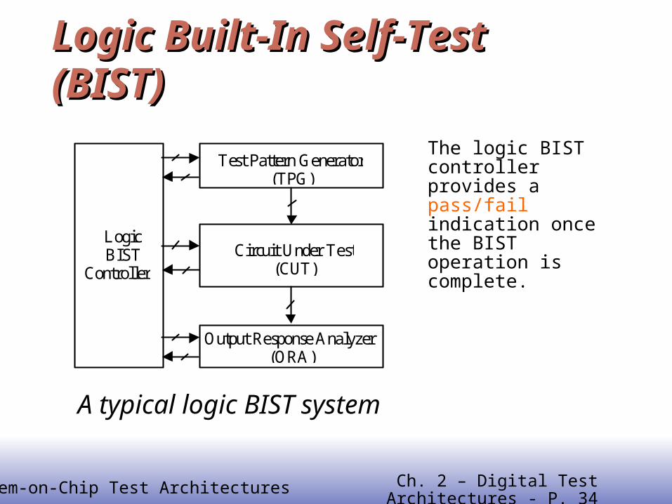
Logic Built-In Self-Test (BIST)Logic Built-In Self-Test (BIST)
A typical logic BIST system
The logic BIST controller provides a pass/fail indication once the BIST operation is complete. Logic
BISTController
Test Pattern Generator(TPG)
Output Response Analyzer(ORA)
Circuit Under Test(CUT)

EE141System-on-Chip Test Architectures Ch. 2 – Digital Test Architectures - P. 35
Logic Built-In Self-TestLogic Built-In Self-Test TPG
Constructed from linear feedback shift register (LFSR) or cellular automata
Exhaustive testing – all possible 2n test patterns Pseudo-random testing – a subset of 2n test
patterns Pseudo-exhaustive testing – 2w or 2k-1 test
patterns, where w < k < n
ORA Constructed from multiple-input signature register
(MISR)

EE141System-on-Chip Test Architectures Ch. 2 – Digital Test Architectures - P. 36
Logic BIST ArchitecturesLogic BIST Architectures
Test-per-Scan BIST Hardware overhead is low
Test-per-Clock BIST Execute tests faster than Test-per-Scan
BIST More hardware overhead
EE141System-on-Chip Test Architectures Ch. 2 – Digital Test Architectures - P. 37
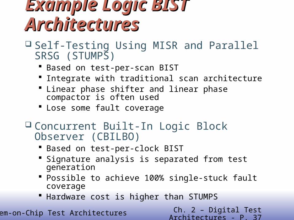
Example Logic BIST ArchitecturesExample Logic BIST Architectures Self-Testing Using MISR and Parallel SRSG
(STUMPS) Based on test-per-scan BIST Integrate with traditional scan architecture Linear phase shifter and linear phase compactor is
often used Lose some fault coverage
Concurrent Built-In Logic Block Observer (CBILBO) Based on test-per-clock BIST Signature analysis is separated from test generation Possible to achieve 100% single-stuck fault coverage Hardware cost is higher than STUMPS

EE141System-on-Chip Test Architectures Ch. 2 – Digital Test Architectures - P. 38
STUMPSSTUMPS
PRPG
MISR
CUT (C)
A STUMPS-based architectureSTUMPS
CUT (C)
Linear Phase Compactor
MISR
Linear Phase Shifter
PRPG
EE141System-on-Chip Test Architectures Ch. 2 – Digital Test Architectures - P. 39
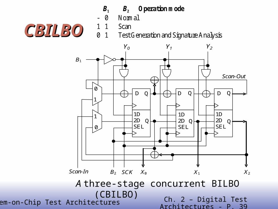
CBILBOCBILBO
A three-stage concurrent BILBO (CBILBO)
B1 B2 Operation mode - 0 Normal 1 1 Scan 0 1 Test Generation and Signature Analysis
Scan-In X0
B1 Y0 Y1 Y2
SCK X1
D Q 0 1
1D 2D SEL
D Q
0 1 1D
2D SEL
Q Q
D Q 1D 2D SEL
Q
B2 X2
Scan-Out
EE141System-on-Chip Test Architectures Ch. 2 – Digital Test Architectures - P. 40
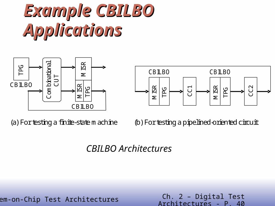
Example CBILBO ApplicationsExample CBILBO Applications
CBILBO CBILBO
CC
1
CC
2
TPG
MIS
R
TPG
MIS
R
CBILBO Architectures
(a) For testing a finite-state machine (b) For testing a pipelined-oriented circuit
MIS
R
MIS
R
TPG
TPG
CBILBO
Com
bina
tiona
l C
UT
CBILBO

EE141System-on-Chip Test Architectures Ch. 2 – Digital Test Architectures - P. 41
Coverage-Driven Logic BIST ArchitecturesCoverage-Driven Logic BIST Architectures
Approaches to Enhance logic BIST Fault Coverage In-field coverage enhancement
– Weighted Pattern Generation– Test Point Insertion– Mixed-Mode BIST
Manufacturing Coverage Enhancement– Hybrid BIST
EE141System-on-Chip Test Architectures Ch. 2 – Digital Test Architectures - P. 42
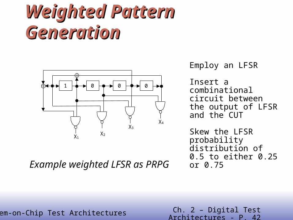
Weighted Pattern GenerationWeighted Pattern Generation
Example weighted LFSR as PRPG
Employ an LFSR
Insert a combinational circuit between the output of LFSR and the CUT
Skew the LFSR probability distribution of 0.5 to either 0.25 or 0.75
X1X2
X3
0
X4
01 0

EE141System-on-Chip Test Architectures Ch. 2 – Digital Test Architectures - P. 43
Test Point InsertionTest Point Insertion
0 1
BIST_mode Control point
Observation point
Typical test point inserted for improving a circuit’s fault coverage
(a) Test point with a multiplexer (b) Test point with AND-OR gates
Observation point
Control point
BIST_mode
EE141System-on-Chip Test Architectures Ch. 2 – Digital Test Architectures - P. 44
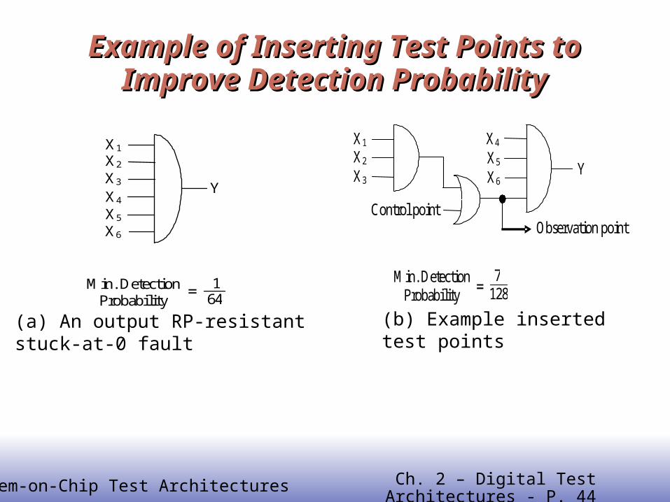
Example of Inserting Test Points to Improve Example of Inserting Test Points to Improve Detection ProbabilityDetection Probability
X1 X2 X3 X4 X5 X6
Y
Min. Detection Probability
= 1 64
(a) An output RP-resistant stuck-at-0 fault (b) Example inserted test points
Observation point Control point
X1 X2 X3
X4 X5 X6
Y
Min. Detection Probability =
7 128

EE141System-on-Chip Test Architectures Ch. 2 – Digital Test Architectures - P. 45
Test Point Placement Use fault simulation Use testability measures to guide them
Control Point Activation During normal operation
– Deactivated During testing
– Random activation– Deterministic activation
Test Point InsertionTest Point Insertion

EE141System-on-Chip Test Architectures Ch. 2 – Digital Test Architectures - P. 46
Mixed-Mode BISTMixed-Mode BIST
ROM Compression Store deterministic patterns in ROM
LFSR Reseeding Generate deterministic patterns by
reseeding LFSR with computed seedsEmbedding Deterministic Patterns
Transform the “useless” patterns into deterministic patterns

EE141System-on-Chip Test Architectures Ch. 2 – Digital Test Architectures - P. 47
Hybrid BISTHybrid BIST
Perform top-up ATPG for the faults not detected by BIST
Store the patterns directly on the testerStore the patterns on the tester in a
compressed form and make use of the existing BIST hardware to decompress them

EE141System-on-Chip Test Architectures Ch. 2 – Digital Test Architectures - P. 48
Low-Power Logic BIST ArchitectureLow-Power Logic BIST ArchitectureLow-Transition BIST Design
Insert an AND gate and a toggle flip-flop at the scan input of the scan chain
Advantages:– Less design intrusive – no performance degradation– Low hardware overhead
Disadvantages:– Low fault coverage – Long test sequence
EE141System-on-Chip Test Architectures Ch. 2 – Digital Test Architectures - P. 49
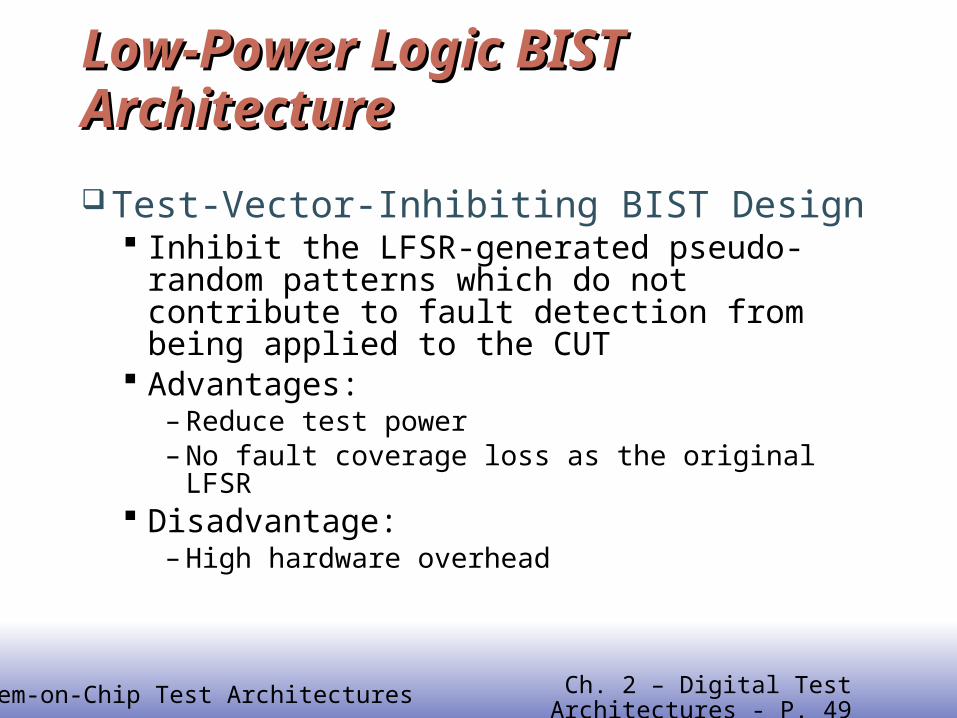
Low-Power Logic BIST ArchitectureLow-Power Logic BIST Architecture
Test-Vector-Inhibiting BIST Design Inhibit the LFSR-generated pseudo-
random patterns which do not contribute to fault detection from being applied to the CUT
Advantages:– Reduce test power– No fault coverage loss as the original LFSR
Disadvantage:– High hardware overhead
EE141System-on-Chip Test Architectures Ch. 2 – Digital Test Architectures - P. 50
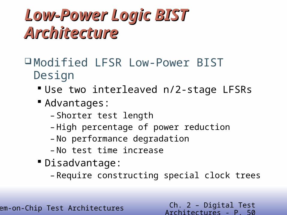
Low-Power Logic BIST ArchitectureLow-Power Logic BIST Architecture
Modified LFSR Low-Power BIST Design Use two interleaved n/2-stage LFSRs Advantages:
– Shorter test length– High percentage of power reduction– No performance degradation– No test time increase
Disadvantage:– Require constructing special clock trees
EE141System-on-Chip Test Architectures Ch. 2 – Digital Test Architectures - P. 51
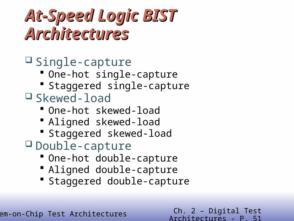
At-Speed Logic BIST ArchitecturesAt-Speed Logic BIST Architectures
Single-capture One-hot single-capture Staggered single-capture
Skewed-load One-hot skewed-load Aligned skewed-load Staggered skewed-load
Double-capture One-hot double-capture Aligned double-capture Staggered double-capture
EE141System-on-Chip Test Architectures Ch. 2 – Digital Test Architectures - P. 52
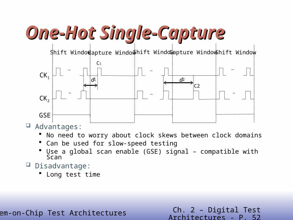
One-Hot Single-CaptureOne-Hot Single-Capture
Advantages: No need to worry about clock skews between clock domains Can be used for slow-speed testing Use a global scan enable (GSE) signal – compatible with Scan
Disadvantage: Long test time
CK1
CK2
GSE
Shift Window Capture Window
… C1
Shift Window
C2
…
Capture Window
…
Shift Window
… … …
d1 d2
EE141System-on-Chip Test Architectures Ch. 2 – Digital Test Architectures - P. 53
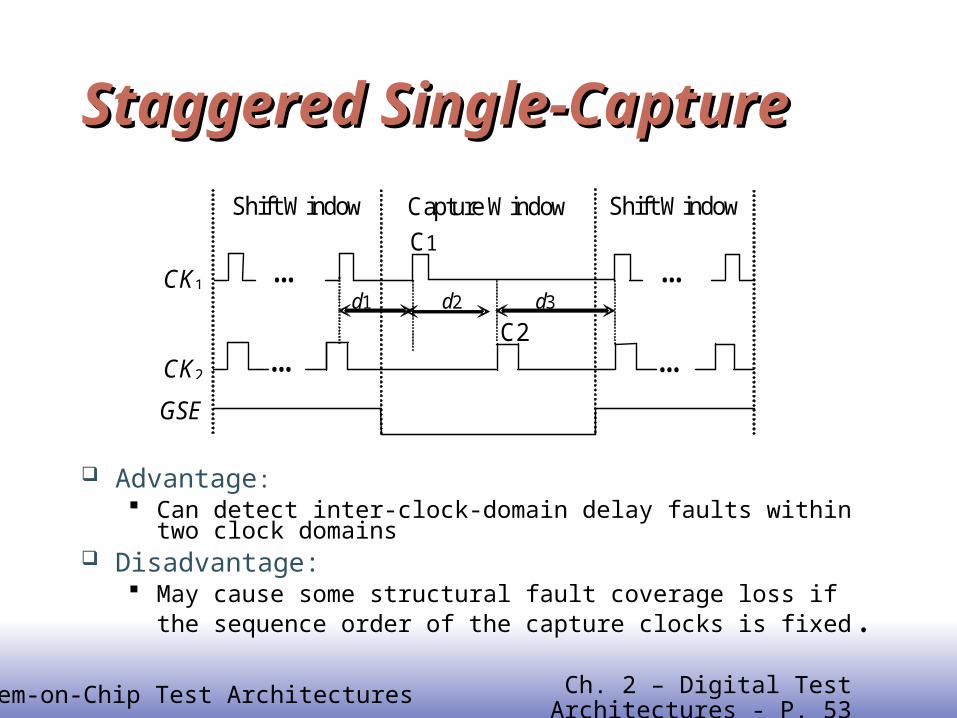
Staggered Single-CaptureStaggered Single-Capture
CK1
CK2
Shift Window Capture Window Shift Window
…
…
…
…
C1
C2
GSE
d2 d3 d1
Advantage: Can detect inter-clock-domain delay faults within two clock domains
Disadvantage: May cause some structural fault coverage loss if the sequence
order of the capture clocks is fixed.

EE141System-on-Chip Test Architectures Ch. 2 – Digital Test Architectures - P. 54
One-Hot Skewed-LoadOne-Hot Skewed-Load
CK1
SE1
Shift Window Capture Window Shift Window Capture Window Shift Window
… … … S1 C1
d1
CK2
SE2
… C2
… … S2
d2
Advantage: Can be used for at-speed testing of intra-clock-domain delay faults
Disadvantages: Cannot be used for testing of inter-clock-domain delay faults Long test time
EE141System-on-Chip Test Architectures Ch. 2 – Digital Test Architectures - P. 55
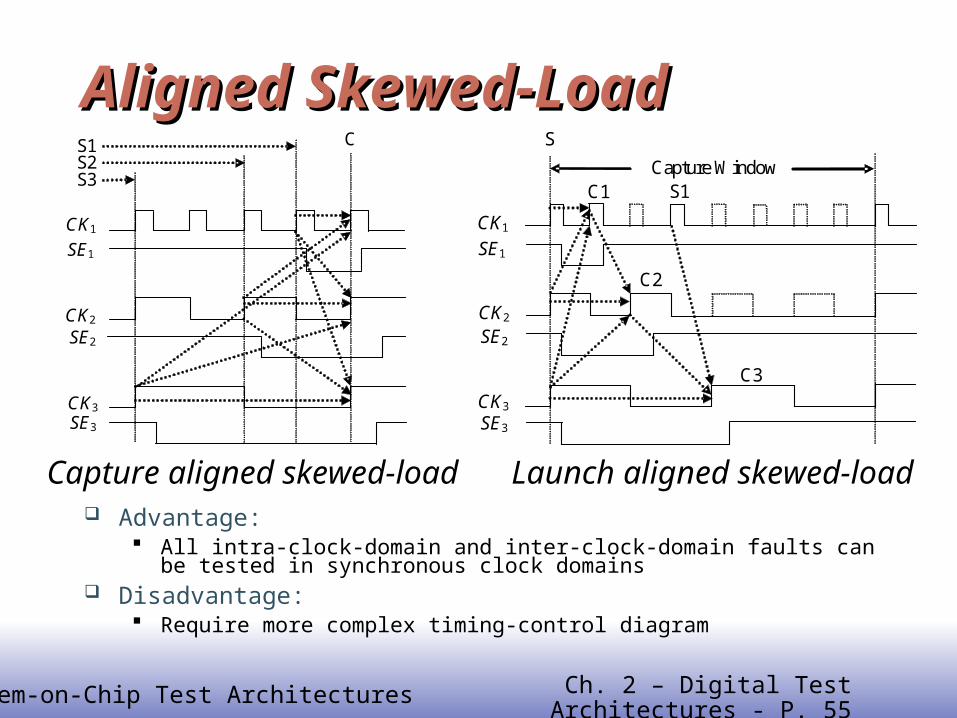
Aligned Skewed-LoadAligned Skewed-Load
S3
CK1
CK2
CK3
SE1
SE2
SE3
S2 S1 C S
CK1
CK2
CK3
SE1
SE2
SE3
Capture Window C1 S1
C3
C2
Capture aligned skewed-load Launch aligned skewed-load Advantage:
All intra-clock-domain and inter-clock-domain faults can be tested in synchronous clock domains
Disadvantage: Require more complex timing-control diagram
EE141System-on-Chip Test Architectures Ch. 2 – Digital Test Architectures - P. 56
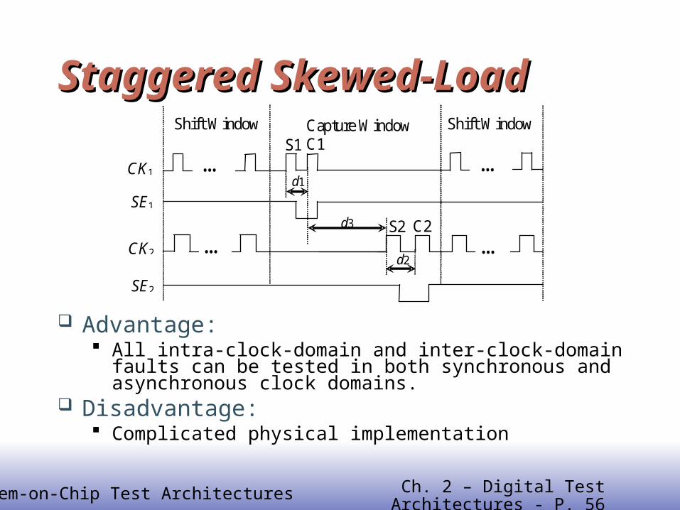
Staggered Skewed-LoadStaggered Skewed-Load
CK1
SE1
Shift Window Capture Window Shift Window
… … S1 C1
d1
d3
CK2
SE2
… C2
… S2
d2
Advantage: All intra-clock-domain and inter-clock-domain faults can be
tested in both synchronous and asynchronous clock domains.
Disadvantage: Complicated physical implementation
EE141System-on-Chip Test Architectures Ch. 2 – Digital Test Architectures - P. 57
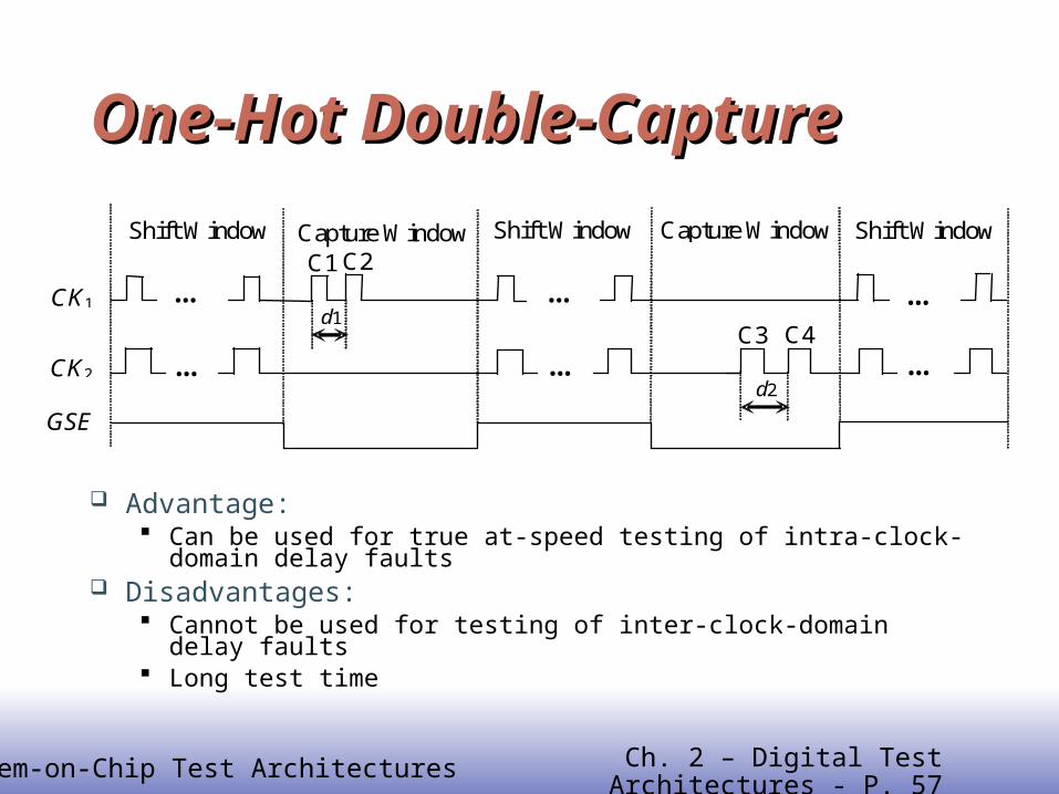
One-Hot Double-CaptureOne-Hot Double-Capture
Shift Window Capture Window Shift Window Capture Window Shift Window
CK1 … … … C1 C2
d1
CK2 … C4
… … C3
d2
GSE
Advantage: Can be used for true at-speed testing of intra-clock-domain delay
faults Disadvantages:
Cannot be used for testing of inter-clock-domain delay faults Long test time
EE141System-on-Chip Test Architectures Ch. 2 – Digital Test Architectures - P. 58
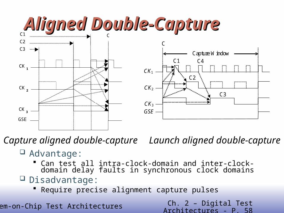
Aligned Double-CaptureAligned Double-Capture C
CK1
CK2
CK3
Capture Window C1 C4
C2
GSE
C3
C3
CK1
CK2
CK3
C2
C1 C
GSE
Capture aligned double-capture Launch aligned double-capture Advantage:
Can test all intra-clock-domain and inter-clock-domain delay faults in synchronous clock domains
Disadvantage: Require precise alignment capture pulses

EE141System-on-Chip Test Architectures Ch. 2 – Digital Test Architectures - P. 59
Staggered Double-CaptureStaggered Double-Capture
CK1
CK2
Shift Window Capture Window Shift Window
…
…
…
…
C1
C2
GSE
d2 d3 d1
Advantages: Ease physical implementation Integrate logic BIST with scan/ATPG
Disadvantage: May cause fault coverage loss due to the ordered
sequence of capture clocks.
EE141System-on-Chip Test Architectures Ch. 2 – Digital Test Architectures - P. 60
Summary of Industry Practices for Summary of Industry Practices for At-Speed Logic BISTAt-Speed Logic BIST
Industry Practices Skewed-load Double-Capture
Encounter Test Through service Through service
ETLogic √ Through service
LBIST Architect √ √TurboBIST-Logic √

EE141System-on-Chip Test Architectures Ch. 2 – Digital Test Architectures - P. 61
Test CompressionTest Compression Decompressor
Add some additional on-chip hardware before the scan chains to decompress the test stimulus
Use lossless compression Compactor
Add some additional on-chip hardware after scan chains to compact the response
The compaction is lossy Advantages:
Reduce ATE memory Reduce test data volume and test application time
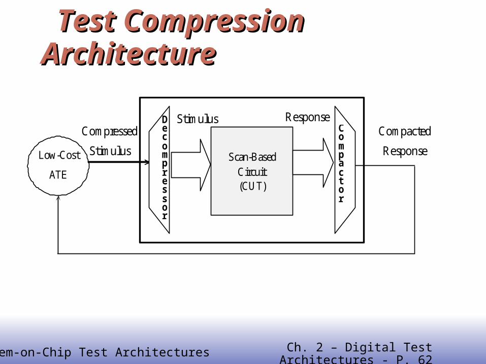
EE141System-on-Chip Test Architectures Ch. 2 – Digital Test Architectures - P. 62
Test Compression ArchitectureTest Compression Architecture
Compressed
Stimulus
Low-Cost
ATE
Scan-Based Circuit (CUT)
Stimulus
Response
Compacted
Response
D e c o m p r e s s o r
C o m p a c t o r

EE141System-on-Chip Test Architectures Ch. 2 – Digital Test Architectures - P. 63
Circuits for Test Stimulus CompressionCircuits for Test Stimulus Compression
Linear-Decompression-Based Schemes Combinational linear decompressors Sequential linear decompressors
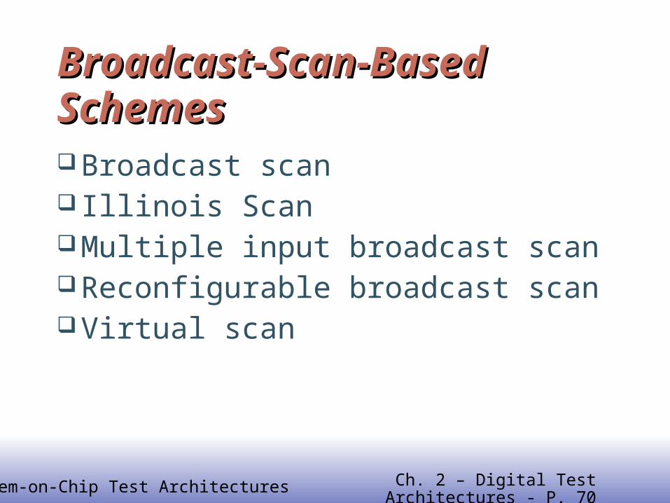
Broadcast-Scan-Based Schemes Broadcast scan Illinois scan Multiple-input broadcast scan Reconfigurable broadcast scan Virtual scan
Comparison
EE141System-on-Chip Test Architectures Ch. 2 – Digital Test Architectures - P. 64
Linear-Decompression-Based SchemesLinear-Decompression-Based Schemes
Linear Decompressor Concept Consists of only XOR gates and Flip-Flops Its output space is a linear subspace that is spanned by a
Boolean matrix.
Combinational Linear Decompressor Consists of only XOR gates
Sequential Linear Decompressor Consists of XOR gates and Flip-Flops Flip-flops provides additional free variables for state encoding.
EE141System-on-Chip Test Architectures Ch. 2 – Digital Test Architectures - P. 65
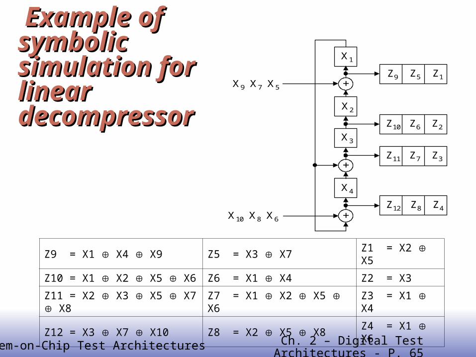
Example of Example of symbolic simulation symbolic simulation for linear for linear decompressor decompressor
Z9 Z5 Z1
Z10 Z6 Z2
+
X1
X2
X3
X9 X7 X5
Z11 Z7 Z3
Z12 Z8 Z4+
X4
X10 X8 X6
+
Z9 = X1 X4 X9 Z5 = X3 X7 Z1 = X2 X5
Z10 = X1 X2 X5 X6 Z6 = X1 X4 Z2 = X3
Z11 = X2 X3 X5 X7 X8 Z7 = X1 X2 X5 X6 Z3 = X1 X4
Z12 = X3 X7 X10 Z8 = X2 X5 X8 Z4 = X1 X6
EE141System-on-Chip Test Architectures Ch. 2 – Digital Test Architectures - P. 66
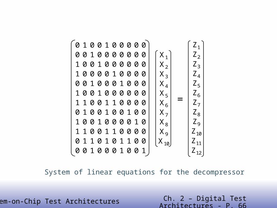
System of linear equations for the decompressor
0 1 0 0 1 0 0 0 0 00 0 1 0 0 0 0 0 0 01 0 0 1 0 0 0 0 0 01 0 0 0 0 1 0 0 0 00 0 1 0 0 0 1 0 0 01 0 0 1 0 0 0 0 0 01 1 0 0 1 1 0 0 0 00 1 0 0 1 0 0 1 0 01 0 0 1 0 0 0 0 1 01 1 0 0 1 1 0 0 0 00 1 1 0 1 0 1 1 0 00 0 1 0 0 0 1 0 0 1
X1
X2
X3
X4
X5
X6
X7
X8
X9
X10
=
Z1
Z2
Z3
Z4
Z5
Z6
Z7
Z8
Z9
Z10
Z11
Z12

EE141System-on-Chip Test Architectures Ch. 2 – Digital Test Architectures - P. 67
Combinational Linear DecompressorCombinational Linear Decompressor
Advantage: Simpler hardware and control because only XOR
gates are used
Disadvantages: Low Encoding Efficiency
– Because no free variables are used– Can be improved by dynamically adjusting the
number of scan chains that are loaded in each clock cycle.
EE141System-on-Chip Test Architectures Ch. 2 – Digital Test Architectures - P. 68
Sequential Linear DecompressorSequential Linear Decompressor Based on linear finite-state machines
Examples: LFSRs, cellular automata, ring generators
Advantages: Allow free variables from earlier clock cycles Much greater flexibility than combinational linear decompressor
Two classes Static reseeding
– Drawbacks The tester is idle while the LFSR is running in autonomous
mode. The LFSR must be at least as large as the number of
specified bits in the test cube.
Dynamic reseeding
EE141System-on-Chip Test Architectures Ch. 2 – Digital Test Architectures - P. 69
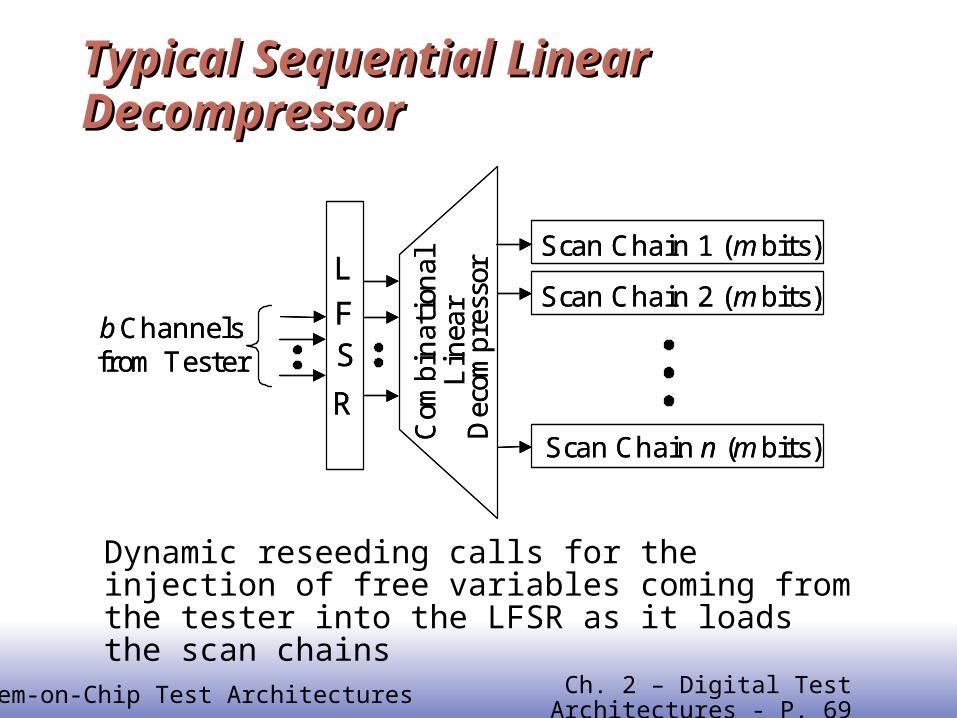
Typical Sequential Linear DecompressorTypical Sequential Linear Decompressor
Dynamic reseeding calls for the injection of free variables coming from the tester into the LFSR as it loads the scan chains
Scan Chain 1 (mbits)
Scan Chain 2 (mbits)
Scan Chain n (mbits)
LFS
R
bChannelsfrom Tester
Com
binat
ional
Lin
ear
Dec
ompr
esso
r Scan Chain 1 (mbits)
Scan Chain 2 (mbits)
Scan Chain n (mbits)
LFS
R
bChannelsfrom Tester
Com
binat
ional
Lin
ear
Dec
ompr
esso
r
EE141System-on-Chip Test Architectures Ch. 2 – Digital Test Architectures - P. 70
Broadcast-Scan-Based SchemesBroadcast-Scan-Based SchemesBroadcast scan Illinois ScanMultiple input broadcast scanReconfigurable broadcast scanVirtual scan

EE141System-on-Chip Test Architectures Ch. 2 – Digital Test Architectures - P. 71
Broadcast ScanBroadcast Scan
- Broadcasting to scan chains driving independent circuit
- Won’t affect fault coverage if all circuits are independent
EE141System-on-Chip Test Architectures Ch. 2 – Digital Test Architectures - P. 72
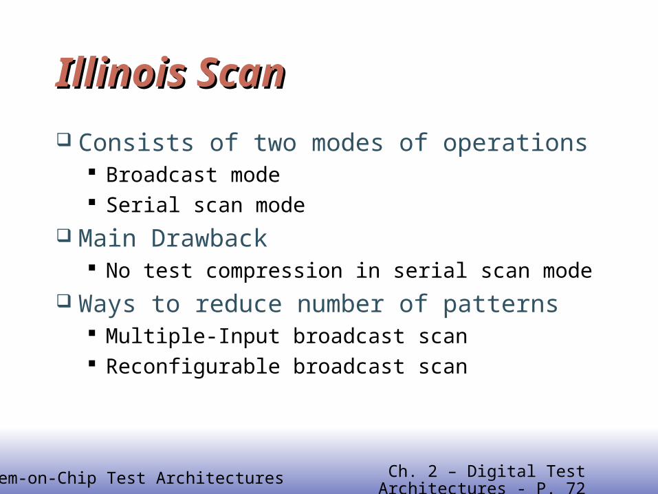
Illinois ScanIllinois Scan
Consists of two modes of operations Broadcast mode Serial scan mode
Main Drawback No test compression in serial scan mode
Ways to reduce number of patterns Multiple-Input broadcast scan Reconfigurable broadcast scan
EE141System-on-Chip Test Architectures Ch. 2 – Digital Test Architectures - P. 73
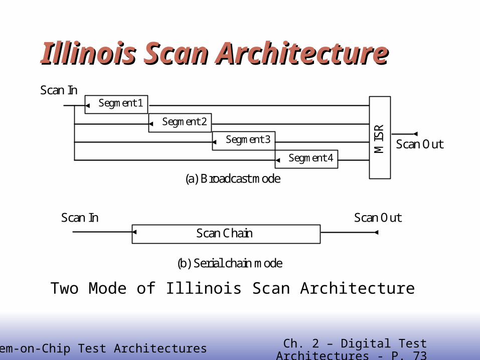
Illinois Scan ArchitectureIllinois Scan Architecture
Two Mode of Illinois Scan Architecture
Scan In Segment 1
Segment 2
Segment 3
Segment 4
MIS
R
Scan Out
(a) Broadcast mode
Scan Chain Scan In Scan Out
(b) Serial chain mode
EE141System-on-Chip Test Architectures Ch. 2 – Digital Test Architectures - P. 74
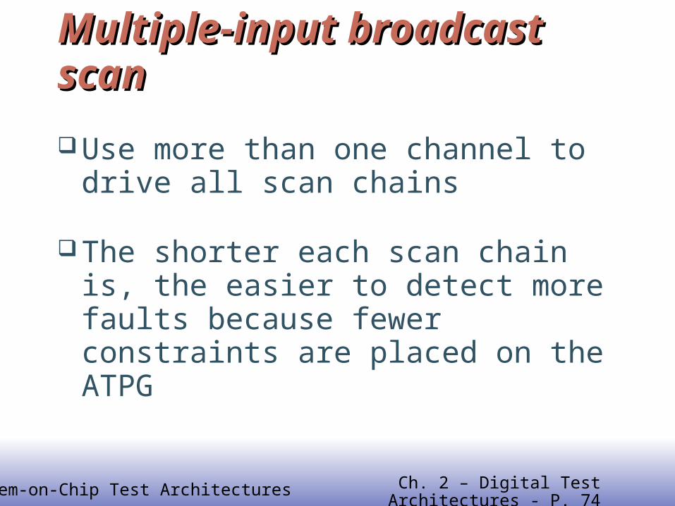
Multiple-input broadcast scanMultiple-input broadcast scan
Use more than one channel to drive all scan chains
The shorter each scan chain is, the easier to detect more faults because fewer constraints are placed on the ATPG
EE141System-on-Chip Test Architectures Ch. 2 – Digital Test Architectures - P. 75
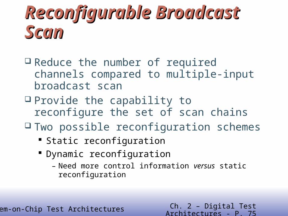
Reconfigurable Broadcast ScanReconfigurable Broadcast Scan
Reduce the number of required channels compared to multiple-input broadcast scan
Provide the capability to reconfigure the set of scan chains
Two possible reconfiguration schemes Static reconfiguration Dynamic reconfiguration
– Need more control information versus static reconfiguration
EE141System-on-Chip Test Architectures Ch. 2 – Digital Test Architectures - P. 76
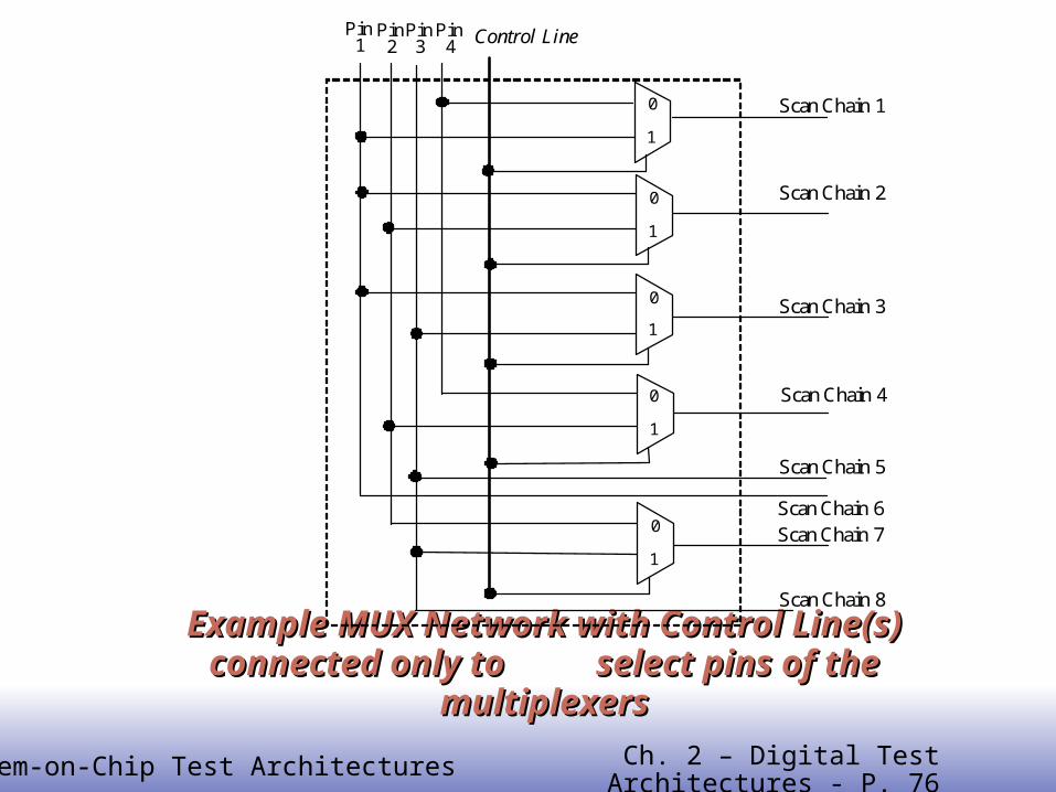
Example MUX Network with Control Line(s) connected only to Example MUX Network with Control Line(s) connected only to select pins of the multiplexers select pins of the multiplexers
Scan Chain 1
Scan Chain 2
Scan Chain 3
Scan Chain 4
Scan Chain 5
Scan Chain 6 Scan Chain 7
Scan Chain 8
0
1
0
1
0
1
0
1
0
1
Pin 1
Pin 2
Pin 3
Pin 4
Control Line
EE141System-on-Chip Test Architectures Ch. 2 – Digital Test Architectures - P. 77
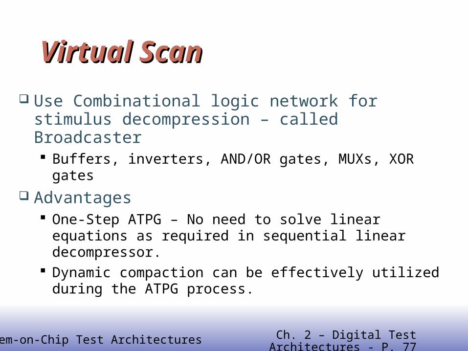
Virtual ScanVirtual Scan
Use Combinational logic network for stimulus decompression – called Broadcaster Buffers, inverters, AND/OR gates, MUXs, XOR gates
Advantages One-Step ATPG – No need to solve linear equations as
required in sequential linear decompressor. Dynamic compaction can be effectively utilized during
the ATPG process.
EE141System-on-Chip Test Architectures Ch. 2 – Digital Test Architectures - P. 78
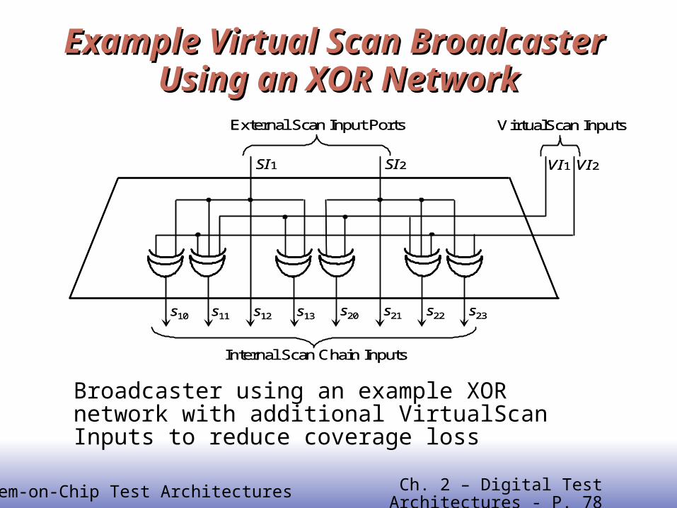
Example Virtual Scan Broadcaster Example Virtual Scan Broadcaster Using an XOR NetworkUsing an XOR Network
Broadcaster using an example XOR network with additional VirtualScan Inputs to reduce coverage loss
SI1 SI2
External Scan Input Ports
VI1 VI2
VirtualScan Inputs
s10 s11 s12 s13 s20 s21 s22 s23
Internal Scan Chain Inputs
SI1 SI2
External Scan Input Ports
VI1 VI2
VirtualScan Inputs
s10 s11 s12 s13 s20 s21 s22 s23
Internal Scan Chain Inputs

EE141System-on-Chip Test Architectures Ch. 2 – Digital Test Architectures - P. 79
Example Virtual Scan Broadcaster Example Virtual Scan Broadcaster Using a MUX NetworkUsing a MUX Network
Broadcaster using an example MUX network with additional VirtualScan inputs that can also be connected to data pins of the multiplexers
s10 s11 s13 s20 s22 s23
Internal Scan Chain Inputs
s21s12
SI1 SI2
External Scan Input Ports
VI1 VI2
VirtualScan Inputs
s10 s11 s13 s20 s22 s23
Internal Scan Chain Inputs
s21s12
SI1 SI2
External Scan Input Ports
VI1 VI2
VirtualScan Inputs
EE141System-on-Chip Test Architectures Ch. 2 – Digital Test Architectures - P. 80
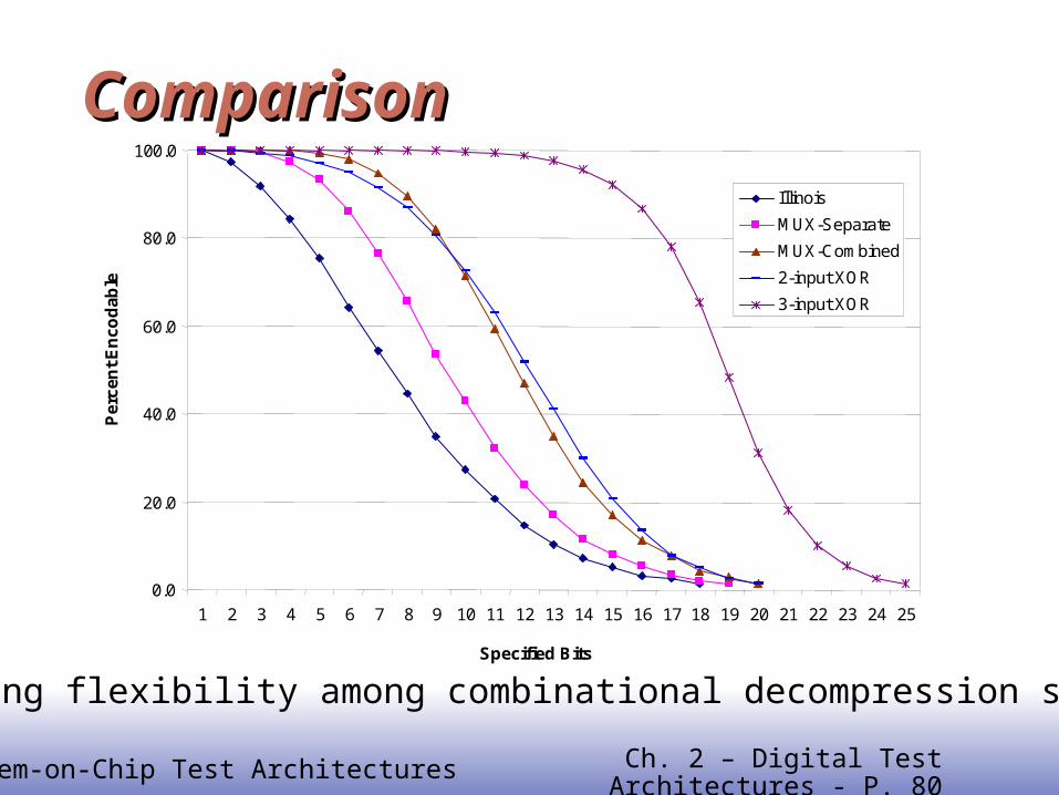
ComparisonComparison
Encoding flexibility among combinational decompression schemes
0.0
20.0
40.0
60.0
80.0
100.0
1 2 3 4 5 6 7 8 9 10 11 12 13 14 15 16 17 18 19 20 21 22 23 24 25
Illinois
MUX-Separate
MUX-Combined
2-input XOR
3-input XOR
Specified Bits
Per
cen
tE
nco
dab
le

EE141System-on-Chip Test Architectures Ch. 2 – Digital Test Architectures - P. 81
Circuits for Test Response CompactionCircuits for Test Response Compaction
Performed at the output of scan chainsTo reduce the amount of test responseGrouped into three categories
Space compaction Time compaction Mixed space and time compaction
EE141System-on-Chip Test Architectures Ch. 2 – Digital Test Architectures - P. 82
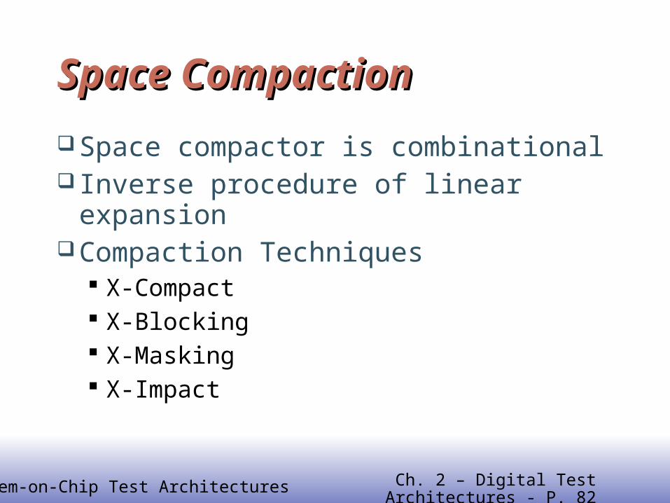
Space CompactionSpace Compaction
Space compactor is combinational Inverse procedure of linear expansionCompaction Techniques
X-Compact X-Blocking X-Masking X-Impact

EE141System-on-Chip Test Architectures Ch. 2 – Digital Test Architectures - P. 83
X-tolerant Response CompactionX-tolerant Response Compaction
An X-compactor with 8 inputs and 5 outputs
Out 1
SC1
XOR XOR XOR XOR XOR XOR XOR XOR XOR XOR
SC2 SC3 SC4 SC5 SC6 SC7 SC 8
XOR
Out 2
XOR
Out 3
XOR
Out 4
XOR
Out 5
XOR
EE141System-on-Chip Test Architectures Ch. 2 – Digital Test Architectures - P. 84
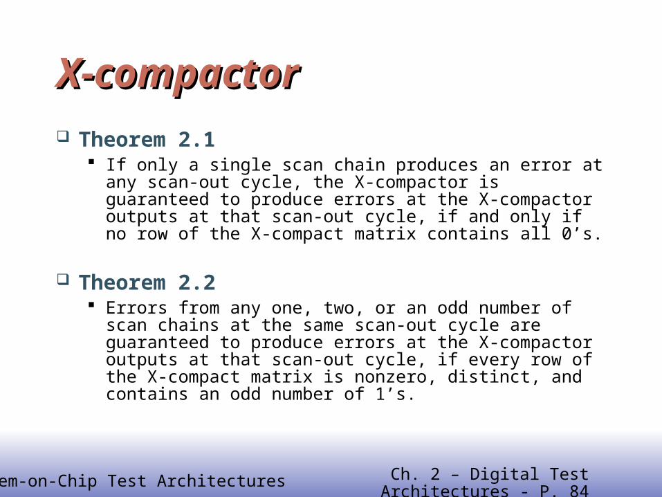
X-compactorX-compactor Theorem 2.1
If only a single scan chain produces an error at any scan-out cycle, the X-compactor is guaranteed to produce errors at the X-compactor outputs at that scan-out cycle, if and only if no row of the X-compact matrix contains all 0’s.
Theorem 2.2 Errors from any one, two, or an odd number of scan chains
at the same scan-out cycle are guaranteed to produce errors at the X-compactor outputs at that scan-out cycle, if every row of the X-compact matrix is nonzero, distinct, and contains an odd number of 1’s.
EE141System-on-Chip Test Architectures Ch. 2 – Digital Test Architectures - P. 85
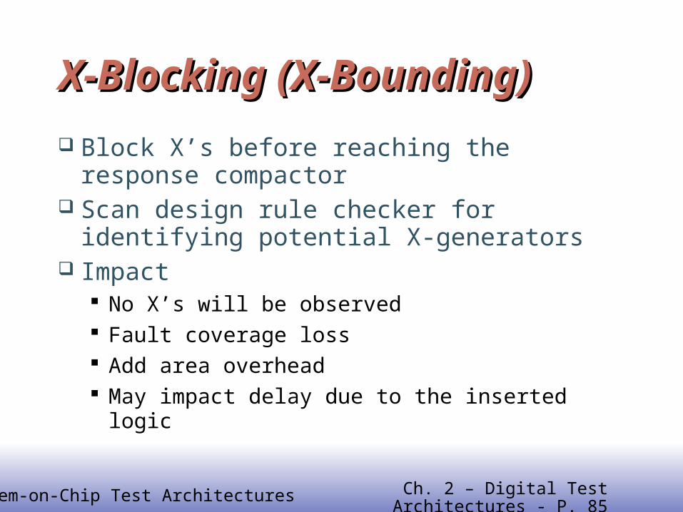
X-Blocking (X-Bounding)X-Blocking (X-Bounding)
Block X’s before reaching the response compactor
Scan design rule checker for identifying potential X-generators
Impact No X’s will be observed Fault coverage loss Add area overhead May impact delay due to the inserted logic
EE141System-on-Chip Test Architectures Ch. 2 – Digital Test Architectures - P. 86
X-MaskingX-Masking
An example X-masking circuit
Mask off X’s right before the response compactor
Scan Out 1
Compactor
Mask Controller
Scan Out 2
Scan Out 3
Mask Bit 1
Mask Bit 2
Mask Bit 3

EE141System-on-Chip Test Architectures Ch. 2 – Digital Test Architectures - P. 87
X-ImpactX-Impact
Handling of X-Impact
G1
G2G3
G4
G5G6
G7
G8
a
bc
de
fgh
f1
p
q
SC1
SC2
SC3
SC4
..1
1
X??
??
? G1
G2G3
G4
G5G6
G7
G8
a
bc
de
fgh
f1
p
q
SC1
SC2
SC3
SC4
..1
1
X??
??
?
EE141System-on-Chip Test Architectures Ch. 2 – Digital Test Architectures - P. 88
XX-Impact-Impact
G1
G2G3
G4
G5G6
G7
G8
a
bc
de
fgh
f2
p
q
SC1
SC2
SC3
SC4
.01
11
? G1
G2G3
G4
G5G6
G7
G8
a
bc
de
fgh
f2
p
q
SC1
SC2
SC3
SC4
.01
11
?
Handling of Aliasing
EE141System-on-Chip Test Architectures Ch. 2 – Digital Test Architectures - P. 89
Time compactionTime compaction
Uses sequential logic to compact test response
No unknown (X) values are allowed to reach the compactor; otherwise X-bounding, X-masking must be employed.
MISR is most widely used
EE141System-on-Chip Test Architectures Ch. 2 – Digital Test Architectures - P. 90
Mixed Time and Space CompactionMixed Time and Space Compaction
Combine the advantages of a time compactor and a space compactor but with high area overhead
Examples of mixed time and space compactors OPMISR Convolutional Compactor q-compactor
– No feedback path

EE141System-on-Chip Test Architectures Ch. 2 – Digital Test Architectures - P. 91
q-compactorq-compactor
An example q-compactor with single output
D
D
D
D
D
inputs
output
EE141System-on-Chip Test Architectures Ch. 2 – Digital Test Architectures - P. 92
Low-Power Test Compression ArchitecturesLow-Power Test Compression Architectures
Low-Power architectures The Bandwidth-match low-power scan design can be used
for test compression
An Example – The UltraScan Architecture Time-Division Demultiplexer (TDDM) Time-Division Multiplexer (TDM) Clock Controller The TDDM/TDM circuit operates at 10 MHz and slow down
the shift clock frequency to 1 MHz resulting in 10X reduction in shift power dissipation

EE141System-on-Chip Test Architectures Ch. 2 – Digital Test Architectures - P. 93
UltraScanUltraScan
Broadcaster
Compactor
s10 s11 s12 s13
ESI1 ESIn
Test Patterns
Test Responses
Expected Responses
ComparatorComparator
ATE
Pass/Fail
t10 t11 t12 t13
sm0 sm1 sm2 sm3
tm0 tm1 tm2 tm3
SO1 SOm
. . .
. . .
. . .
VirtualScanCircuit
Full-ScanCircuit
. . .
. . .
Broadcaster
TDM
s10 s11 s12 s13
SI1 SI
Comparator
sm0 sm1 sm2 sm3
t m m
ESO1 ESOn
VirtualScanInputs
TDDM
m
. . .
. . .
ClockController
ck1
ck1
ck2

EE141System-on-Chip Test Architectures Ch. 2 – Digital Test Architectures - P. 94
Summary of Industry Practices for Summary of Industry Practices for Test CompressionTest Compression
Industry Practices Stimulus Decompressor Response Compactor
XOR Compression or OPMISR+
Combinational XOR network or Fanout Network
XOR network with or
Without MISR
TestKompress Ring generator XOR network
VirtualScan Combinational logic network XOR network
DFT MAX Combinational MUX network XOR network
ETCompression (Reseeding)PRPG MISR
UtralScan TDDM TDM

EE141System-on-Chip Test Architectures Ch. 2 – Digital Test Architectures - P. 95
Summary of Industry Practices for Summary of Industry Practices for At-Speed Delay Fault TestingAt-Speed Delay Fault Testing
Industry Practices Skewed-Load Double-Capture
XOR Compression or OPMISR+ √ √TestKompress √ √
VirtualScan √ √DFT MAX √ √
ETCompression √ Through service
UtralScan √ √
EE141System-on-Chip Test Architectures Ch. 2 – Digital Test Architectures - P. 96
Random-Access Scan DesignRandom-Access Scan Design Eliminate problems in serial scan mode
Excessive dynamic power during capture difficult fault diagnosis
Scan cell randomly and uniquely addressable Similar to storage cell in random-access memory
(RAM)
Impacts Low shift power dissipation with an increase in
routing overhead Combinational logic diagnosis techniques for locating
faults

EE141System-on-Chip Test Architectures Ch. 2 – Digital Test Architectures - P. 97
Random-Access Scan ArchitecturesRandom-Access Scan Architectures Traditional Random-Access Scan (RAS) Architecture
All scan cells are organized into a two-dimensional array Advantage
– Can reduce shift power dissipation
Disadvantages – No guarantee to reduce test application time or test data volume
– High area overhead
Progressive Random-Access Scan Design (PRAS) Use a structure similar to SRAM or a grid-addressable latch
Shift-Addressable Random-Access Scan Design (STAR)
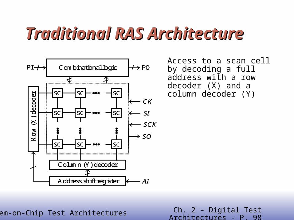
EE141System-on-Chip Test Architectures Ch. 2 – Digital Test Architectures - P. 98
Traditional RAS ArchitectureTraditional RAS Architecture
Access to a scan cell by decoding a full address with a row decoder (X) and a column decoder (Y)
Combinational logic
Column (Y) decoder
SC
AI
PI PO
SC SC…
SC SC SC…
…
SC SC SC
… …
Ro
w (
X)
dec
od
er
Address shift register
SI
SO
SCK
CK
…
Combinational logic
Column (Y) decoder
SC
AI
PI PO
SC SC…
SC SC SC…
…
SC SC SC
… …
Ro
w (
X)
dec
od
er
Address shift register
SI
SO
SCK
CK
…

EE141System-on-Chip Test Architectures Ch. 2 – Digital Test Architectures - P. 99
Traditional RAS Scan CellTraditional RAS Scan Cell
Traditional Scan Cell Design Broadcast the external SI port to all scan cells, cause routing problem
Toggle Scan Cell Design Require a clear mechanism to reset all scan cells prior to testing
.0
1SI
DI
AS
SI
Q
SETM
QD
CK
.0
1SI
DI
AS
SI
Q
SETM
QD
CK
.D DI
AS
SI
Q
SE
Q
.CKQ
.
PO.D DI
AS
SI
Q
SE
Q
.CKQ
.
PO

EE141System-on-Chip Test Architectures Ch. 2 – Digital Test Architectures - P. 100
PRAS DesignPRAS Design
PRAS Scan Cell Design
In normal mode, RE is set to 0, forcing each scan cell to act as a normal D flip-flop.
In test mode, RE is set to 0and a pulse is applied on clock Φ
To read out, clock Φ is held at 1,RE for the selected scan cell is set to 1, and the content of the scan cell is read out through the bidirectional scan data signals SD and SD_.
To write or update a scan value into the scan cell, clock Φ is held at 1, RE for the selected scan cell is set to 1, and the scan value and its complement are appliedon SD and SD_, respectively
D Q
Ф Ф
Ф
RE
SD SD
Ф ФФ
D Q
Ф ФФ
Ф
RE
SD SD
ФФ ФФФ

EE141System-on-Chip Test Architectures Ch. 2 – Digital Test Architectures - P. 101
PRAS DesignPRAS Design
PRAS Architecture
Rows are enabled in a fixed order. It is only necessary to supply a column address to specify which scan cell in an enabled row to access.
Column line drivers
SC
PI
PO
SC SC…
SC SC SC…
…
SC SC SC
… …
Row
ena
ble
shif
t reg
iste
r
Column address decoder
Testcontrollogic
…
…
…
CA
Sense-amplifiers & MISR…
TMSI/SO
Com
bina
tiona
l log
icCK
Column line drivers
SC
PI
PO
SC SC…
SC SC SC…
…
SC SC SC
… …
Row
ena
ble
shif
t reg
iste
r
Column address decoder
Testcontrollogic
…
…
…
CA
Sense-amplifiers & MISR…
TMSI/SO
Com
bina
tiona
l log
icCK

EE141System-on-Chip Test Architectures Ch. 2 – Digital Test Architectures - P. 102
PRAS Test ProcedurePRAS Test Procedurefor each test vector vi (i = 1, 2, …, N) {
/* Test stimulus application *//* Test response compression */enable TM;for each row rj (j = 1, 2, …, m) {
read all scan cells in rj / update MISR;for each scan cell SC in rj
/* v(SC): current value of SC *//* vi(SC): value of SC in vi */
if v(SC) vi(SC) update SC;
}/* Test response acquisition */disable TM;apply the normal clock;
}scan-out MISR as the final test response;
for each test vector vi (i = 1, 2, …, N) {/* Test stimulus application *//* Test response compression */enable TM;for each row rj (j = 1, 2, …, m) {
read all scan cells in rj / update MISR;for each scan cell SC in rj
/* v(SC): current value of SC *//* vi(SC): value of SC in vi */
if v(SC) vi(SC) update SC;
}/* Test response acquisition */disable TM;apply the normal clock;
}scan-out MISR as the final test response;
EE141System-on-Chip Test Architectures Ch. 2 – Digital Test Architectures - P. 103
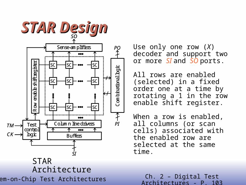
STAR DesignSTAR Design
STAR Architecture
Use only one row (X) decoder and support two or more SI and SO ports.
All rows are enabled (selected) in a fixed order one at a time byrotating a 1 in the row enable shift register.
When a row is enabled, all columns (or scan cells) associated with the enabled row are selected at the same time.Column line drivers
SC
PI
PO
SC SC…
SC SC SC…
…
SC SC SC
… …
Row
ena
ble
shif
t reg
iste
r
Buffers
Testcontrollogic
…
…
…
SI
Sense-amplifiers…
TM
Com
bina
tiona
l log
ic
CK
SO
Column line drivers
SC
PI
PO
SC SC…
SC SC SC…
…
SC SC SC
… …
Row
ena
ble
shif
t reg
iste
r
Buffers
Testcontrollogic
…
…
…
SI
Sense-amplifiers…
TM
Com
bina
tiona
l log
ic
CK
SO

EE141System-on-Chip Test Architectures Ch. 2 – Digital Test Architectures - P. 104
STAR Test ProcedureSTAR Test Procedurefor each test vector vi (i = 1, 2, …, N) {
/* Test stimulus application *//* Test response compression */enable TM;for each row rj (j = 1, 2, …, m) {
read all scan cells in rj / update MISR;/* Update selected rows */update all scan cells in rj;
}/* Test response acquisition */disable TM;apply the normal clock;
}scan-out MISR as the final test response;
for each test vector vi (i = 1, 2, …, N) {/* Test stimulus application *//* Test response compression */enable TM;for each row rj (j = 1, 2, …, m) {
read all scan cells in rj / update MISR;/* Update selected rows */update all scan cells in rj;
}/* Test response acquisition */disable TM;apply the normal clock;
}scan-out MISR as the final test response;

EE141System-on-Chip Test Architectures Ch. 2 – Digital Test Architectures - P. 105
Test Compression RAS ArchitectureTest Compression RAS Architecture
RAS design is effective in reducing shift power dissipation
RAS is achieved power reducing at the cost of increased area and routing overhead
RAS cannot reduce test data volume and test application time significantly
Test compression schemes are applicable for RAS design

EE141System-on-Chip Test Architectures Ch. 2 – Digital Test Architectures - P. 106
STAR Compression ArchitectureSTAR Compression ArchitectureA decompressor is used to decompress the ATE-supplied stimuli.
A compactor is used to compact the test responses.
Column line driver
SC
PI
PO
SC SC…
SC SC SC…
…
SC SC SC
… …
Ro
w e
nab
le s
hif
t re
gis
ter
Decompressor
Testcontrollogic
…
…
…
SI
Compactor…
TMC
om
bin
atio
nal
lo
gic
CK
SO
Column line driver
SC
PI
PO
SC SC…
SC SC SC…
…
SC SC SC
… …
Ro
w e
nab
le s
hif
t re
gis
ter
Decompressor
Testcontrollogic
…
…
…
SI
Compactor…
TMC
om
bin
atio
nal
lo
gic
CK
SO
EE141System-on-Chip Test Architectures Ch. 2 – Digital Test Architectures - P. 107
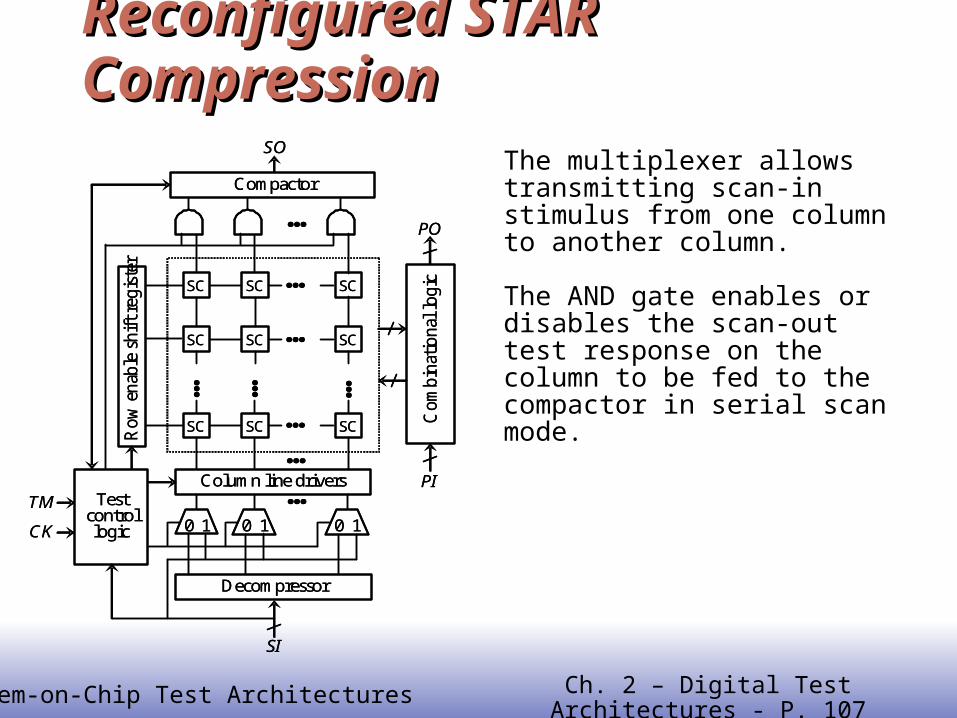
Reconfigured STAR CompressionReconfigured STAR CompressionThe multiplexer allows transmitting scan-in stimulus from one column to another column.
The AND gate enables or disables the scan-out test response on the column to be fed to the compactor in serial scan mode.
Column line drivers
SC
PI
PO
SC SC…
SC SC SC…
…
SC SC SC
… …
Ro
w e
nab
le s
hif
t re
gis
ter
Decompressor
Testcontrollogic
…
…
…
SI
Compactor
…
TM
Co
mb
inat
ion
al l
og
ic
CK
SO
0 1 0 1 10
Column line drivers
SC
PI
PO
SC SC…
SC SC SC…
…
SC SC SC
… …
Ro
w e
nab
le s
hif
t re
gis
ter
Decompressor
Testcontrollogic
…
…
…
SI
Compactor
…
TM
Co
mb
inat
ion
al l
og
ic
CK
SO
0 1 0 1 10

EE141System-on-Chip Test Architectures Ch. 2 – Digital Test Architectures - P. 108
At-Speed RAS ArchitecturesAt-Speed RAS Architectures Major advantages of RAS design
Significant shift power reduction Facilitating fault diagnosis
Additional benefit for at-speed delay fault testing Launch-on-shift (a.k.a. skewed-load) Launch-on-capture (a.k.a. double-capture)
Enhanced-scan based at-speed RAS Design Maximize delay fault detection capability Long vector count problem
EE141System-on-Chip Test Architectures Ch. 2 – Digital Test Architectures - P. 109
At-Speed RAS ArchitecturesAt-Speed RAS Architectures Approaches to overcoming long vector count problem
Using Enhanced-scan-based at-speed RAS architecture
Using Conventional launch-on-capture schemes
Launch-on-capture based at-speed RAS architecture Allow multiple transitions on the initialization vector; thereby
reducing the vector count.
Hybrid at-speed RAS architecture First generate transition fault tests using launch-on-capture
Then supplement the tests using enhanced scan
Faster-than-at-speed RAS architecture To catch small delay defects that escape traditional transition fault
tests.

EE141System-on-Chip Test Architectures Ch. 2 – Digital Test Architectures - P. 110
Concluding RemarksConcluding Remarks Scan and Logic built-in self-test (BIST) are two most widely
used DFT techniques ATPG can no longer guarantee adequate product quality;
at-speed delay testing and test compression become a requirement for 90-nanometer designs and below.
Physical failures can escape detection of ATPG; logic BIST and low-power testing are gaining more industry acceptance in VLSI designs at 65-nanometer and below.
Challenges lie ahead whether pseudo-exhaustive testing will become a preferred BIST pattern generation technique and random-access scan will be a promising DFT technique for test power reduction.