effect of substrate annealing on the quality of pulsed laser deposited zn1−xmgxo thin films
TRANSCRIPT
Applied Surface Science 255 (2009) 7017–7020
Effect of substrate annealing on the quality of pulsed laser depositedZn1�xMgxO thin films
Gaurav Shukla, Alika Khare *
Laser and Photonics Lab, Department of Physics, Indian Institute of Technology Guwahati, Guwahati 781039, India
A R T I C L E I N F O
Article history:
Received 16 January 2009
Received in revised form 10 March 2009
Accepted 10 March 2009
Available online 21 March 2009
Keywords:
Thin films
Deposition
Epitaxial growth
A B S T R A C T
The annealing effects of sapphire substrate before deposition on the quality of epitaxial Zn1�xMgxO thin
films grown by pulsed laser deposition are reported. Our Experimental results indicate that the surface
quality of Zn1�xMgxO thin films and hexagonal columnar growth is improved on the annealed sapphire
substrate at high temperatures due to formation of atomic terraces on the substrate surface. The
photoluminescence signals also increases with the increasing annealing temperature of the substrate.
� 2009 Elsevier B.V. All rights reserved.
Contents lists available at ScienceDirect
Applied Surface Science
journa l homepage: www.e lsev ier .com/ locate /apsusc
1. Introduction
The wide direct band gap Zn1�xMgxO material system is anexcellent choice for optoelectronic devices in the ultraviolet (UV)portion of the spectrum [1]. Zn1�xMgxO possesses tunable bandgap energy from 3.3 eV to 7.8 eV for x = 0 to x = 1, respectively [2–4], relatively low thin film growth temperatures (100–750 8C) [4],intrinsic visible blindness and radiation hardness [5], which arerequired for practical optoelectronic devices. Different depositiontechniques have been used to grow Zn1�xMgxO films on varioussubstrates viz. sapphire, silicon, ZnO, and glass. Among them, thesapphire substrate is preferred for deposition of Zn1�xMgxO filmsfor optoelectronic devices [6]. Sapphire substrates are found tosupport epitaxial growth of wide band gap materials besidespossessing unique properties such as hardness, chemical inertness,high melting point and optical transparency. In some of the cases,the surface treatment of the substrate prior to deposition improvesthe growth and the quality of thin films [7,8]. The surfacetreatment can be performed by plasma pre-conditioning [8] or byannealing the substrate under different environment beforedeposition [9]. The annealing, being a simplest technique for thesurface treatment, results into the ultra-smooth surfaces withatomic steps [10]. These well defined atomic steps act as anucleation center, facilitating the hexagonal growth of the thinfilm. Although there are few reports on growing Zn1�xMgxO thinfilms on sapphire substrates by pulsed laser deposition technique
* Corresponding author. Tel.: +91 361 2582705; fax: +91 361 2582749.
E-mail address: [email protected] (A. Khare).
0169-4332/$ – see front matter � 2009 Elsevier B.V. All rights reserved.
doi:10.1016/j.apsusc.2009.03.033
[4,6,11], there is no report on the effects of the sapphire substrateannealing on epitaxial Zn1�xMgxO films. In this paper, we reportannealing effects of the sapphire substrate on the properties ofZn1�xMgxO films grown by pulsed laser deposition technique inoxygen ambient.
2. Experimental setup
The second harmonic of Q switched Nd:YAG laser was focusedon to sintered Zn1�xMgxO target with a lens of focal length of35 cm. ZnO–MgO composite targets with MgO contents from0 mol.% to 40 mol.% were used during the deposition. Thecomposite targets were made by the standard pressing andsintering method. The target was mounted inside the vacuumchamber through a motorized vacuum feed through and con-tinuously moved in order to avoid piercing with the repeated shotsof laser. The chamber was initially evacuated to a base pressure of10�5 mbar and then filled with O2 gas at the pressure of 10�1 mbar.Zn1�xMgxO thin films were deposited on ultra sonically cleaned c-axis (0 0 0 1) sapphire (a-Al2O3) substrates placed parallel to and4 cm apart from the target. The detailed schematic of theexperimental setup is given elsewhere [12]. All the depositionsof Zn1�xMgxO thin films were made at 700 8C substrate tempera-ture and deposition time was kept fixed for 20 min. Annealing ofthe (0 0 0 1) sapphire substrates was performed in a furnace attemperatures between 800 8C and 1200 8C in air for 2 h beforemounting inside the chamber for deposition. Zn1�xMgxO thin filmswere analyzed with X-ray diffraction (XRD) (SEIFERT) for thecrystal structure and surface morphology was studied by scanningelectron microscope (SEM) (LEO 1430 vp) and atomic force

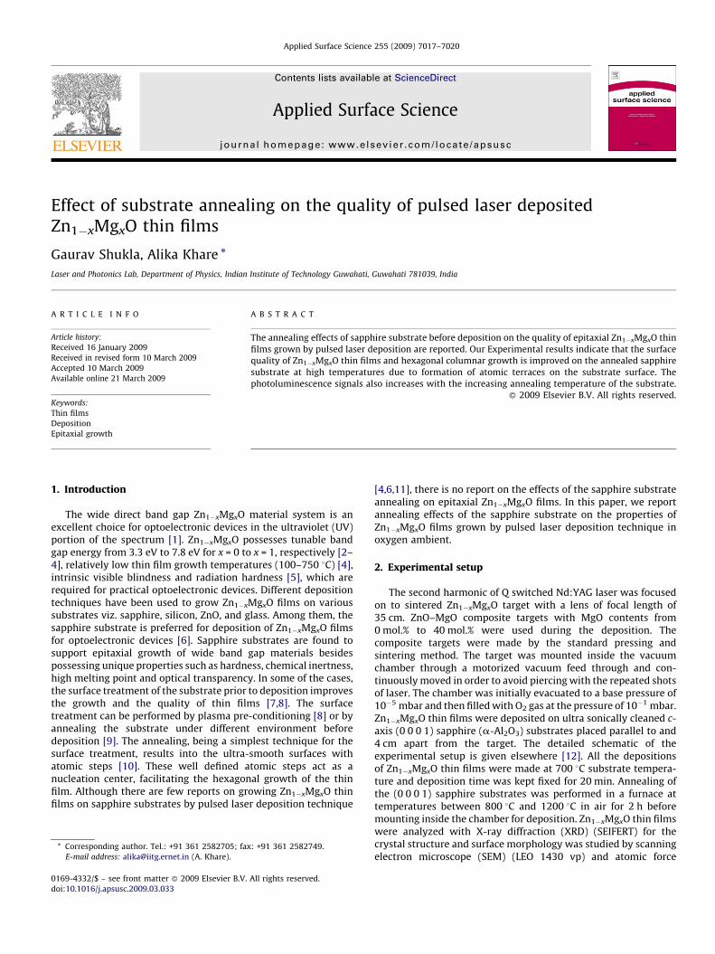
Fig. 1. AFM scans of (a) unannealed sapphire surface, (b) 1200 8C annealed sapphire surface, (c) Zn1�xMgxO (x = 0.1) thin film surface deposited on unannealed sapphire, (d)
Zn1�xMgxO (x = 0.1) thin film surface deposited on 1200 8C annealed sapphire.
Fig. 2. XRD patterns of Zn1�xMgxO (x = 0.1) films deposited at 700 8C substrate
temperature on unannealed and annealed sapphire substrates (inset shows
expanded view of Zn0.9Mg0.1O (0 0 0 2) peak).
G. Shukla, A. Khare / Applied Surface Science 255 (2009) 7017–70207018
microscope (AFM) (NT-MDT-SMENA). Photoluminescence (PL)spectra was recorded by luminescence spectrometer (Thermo-Spectronic-Aminco Bowman Series 2) using a xenon arc lamp asthe excitation source. The excitation wavelength was kept fixed at325 nm. All measurements were carried out at room temperature.
3. Results and discussion
Fig. 1(a) and (b) shows the AFM images of the surface of thepolished unannealed and annealed sapphire substrates, respec-tively. For the substrate without annealing, there were irregularsmall corrugations ranging over the entire surface, as shown inFig. 1(a). The AFM image of sapphire substrate annealed at1200 8C for 2 h shows the drastic change in surface morphologyas shown in Fig. 1(b). The terrace like structure on the substratesurface with atomic steps was formed after annealing. Thepossible mechanism of step formation over annealed sapphiresurface can be explained as follows: the lattice structure of a-Al2O3 along h0 0 0 1i direction can be described by a succession ofdistorted hexagonal compact layers of oxygen atoms sandwich-ing between two close layers of aluminum atoms. The hexagonalunit cell height comprises therefore six layers of oxygen and sixsuch double layers of aluminum. Upon high temperatureannealing, total surface energy of (0 0 0 1) Al2O3 surface tendto increase. In order to maintain a lowest surface energy state,atomic layers of Al and O shift in a direction determined by themiscut orientation of a-Al2O3. Initially at low annealing tem-peratures, formation of monosteps with c/6 height takes place,
where c is the lattice constant of Al2O3. Further increase intemperature gives rise to coalescence process which involves‘‘zipping’’ of monosteps into a double height step. At tempera-tures �1200 8C, the growth of multiheight steps results from

Fig. 3. SEM images of Zn1�xMgxO (x = 0.1) films deposited on (a) unannealed sapphire, (b) 1200 8C annealed sapphire.
G. Shukla, A. Khare / Applied Surface Science 255 (2009) 7017–7020 7019
direct coalescence of lower multiple steps and from displace-ments of monosteps originated from the thermal parting ofmultiheight steps [13,14]. It may be noted further that nochanges in chemical nature of reconstructed sapphire surface hasbeen observed upon annealing in air up to a temperature of1400 8C [15].
Fig. 1(c) and (d) shows AFM scans of pulsed laser depositedZn1�xMgxO (x = 0.1) thin films on unannealed and 1200 8C annealedsapphire substrates, respectively. The rms roughness decreased forZn1�xMgxO (x = 0.1) films deposited on annealed sapphire to 3.2 nmas compared to 5.8 nm for unannealed sapphire.
Fig. 2 shows the X-ray diffraction (XRD) of Zn1�xMgxO filmsdeposited on unannealed (0 0 0 1) sapphire substrates andannealed (0 0 0 1) sapphire substrates. All the films showed apreferential c-axis orientation (0 0 0 2). The intensity of the(0 0 0 2) Zn1�xMgxO peak on annealed sapphire substrates waslarger than that of the unannealed sapphire substrate and theFWHM value of the (0 0 0 2) Zn1�xMgxO peak on annealed sapphiresubstrates was smaller than that of the unannealed sapphiresubstrate. The intensity of the (0 0 0 2) Zn1�xMgxO peak in the XRDspectra increases with increasing annealing temperature, whilethe FWHM values of the (0 0 0 2) Zn1�xMgxO peak decrease on theannealed sapphire substrates, which shows that the annealing ofthe sapphire substrate prior to film deposition can improve theZn1�xMgxO film quality grown by pulsed laser deposition.
SEM images of Zn1�xMgxO (x = 0.1) thin films deposited at700 8C on unannealed and annealed (0 0 0 1) sapphire substrates
Fig. 4. PL spectra of Zn1�xMgxO (x = 0.1) films deposited at 700 8C substrate
temperature on unannealed and annealed sapphire substrates.
are shown in Fig. 3(a) and (b), respectively. The columnarhexagonal growth of Zn1�xMgxO thin films is clearly visible inboth the films. However, Zn1�xMgxO (x = 0.1) thin films depositedon unannealed sapphire showed slanted columnar growth anduneven top surface. Where as Zn1�xMgxO films deposited onannealed sapphire showed excellent vertical growth with veryclean top surface profile.
The annealing at high temperature resulted in the formation ofatomic steps on the substrate surface with reduced surface energystate. The formation of the terrace structure is probably the originof the growth of the highly c-axis oriented film, as well-definedsteps of the sapphire substrate can act as preferred nucleation sitesfor film growth. Thus terrace structure facilitates smooth verticalcolumnar growth and reduces strain in column formation duringthe growth of Zn1�xMgxO other than those caused by the latticemismatch.
Fig. 4 shows the PL spectra of Zn1�xMgxO (x = 0.1) filmsdeposited on to the unannealed and annealed substrates at 800 8Cand 1200 8C, respectively. The PL spectra shows a strong UVemission having peak at 364 nm. The intensity of UV emission peakis higher on annealed sapphire substrates and increases with theannealing temperature. This can be related with the verticalcolumnar growth of the Zn1�xMgxO films deposited at hightemperature pre-annealed substrates.
4. Conclusion
We have reported the annealing effects of sapphire substrateson the Zn1�xMgxO (x = 0.1) films grown by pulsed laser depositionfor the first time to our knowledge. The annealing of the sapphiresubstrate prior to the growth greatly influences the crystallinequalities of the Zn1�xMgxO films. SEM images confirm excellentvertical columnar growth of the thin films. The enhancement inUV-PL signal is observed at higher annealing temperatures. Thissuggests that an optimized annealing of the substrate prior to thefilm growth improves the material qualities of the Zn1�xMgxOepitaxial layer.
References
[1] S.S. Hullavarad, S. Dhar, B. Varughese, I. Takeuchi, T. Venkatesan, R.D. Vispute, J.Vac. Sci. Technol. A 23 (2005) 982.
[2] J. Narayan, A.K. Sharma, A. Kvit, C. Jin, J.F. Muth, O.W. Holland, Solid StateCommun. 121 (2002) 9.
[3] A. Ohtomo, M. Kawasaki, T. Koida, K. Masubuchi, H. Koinuma, Y. Sakurai, Y.Yoshida, T. Yasuda, Y. Segawa, Appl. Phys. Lett. 72 (1998) 2466.
[4] S. Choopun, R.D. Vispute, W. Yang, R.P. Sharma, T. Venkatesan, H. Shen, Appl. Phys.Lett. 80 (2002) 1529.
[5] F.D. Auret, S.A. Goodman, M. Hayes, M.J. Legodi, H.A. van Laarhoven, D.C. Look,Appl. Phys. Lett. 79 (2001) 3074.
[6] W. Yang, R.D. Vispute, S. Choopun, R.P. Sharma, T. Venkatesan, H. Shen, Appl. Phys.Lett. 78 (2001) 2787.

G. Shukla, A. Khare / Applied Surface Science 255 (2009) 7017–70207020
[7] J.H. Kim, S.C. Choi, J.Y. Choi, K.S. Kim, G.M. Yan, C.H. Hong, K.Y. Lim, H.J. Lee, Jpn. J.Appl. Phys. 38 (1999) 2721.
[8] C. Heinlein, J. Grepstad, H. Riechert, R. Averbeck, Mater. Sci. Eng. B 43 (1997) 253.[9] S.F. Chichibu, T. Yoshida, T. Onuma, H. Nakanishi, J. Appl. Phys. 91 (2002) 874.
[10] M. Yoshimoto, T. Maeda, T. Ohnishi, H. Koinuma, O. Ishiyama, M. Shinohara, M.Kubo, R. Miura, A. Miyamoto, Appl. Phys. Lett. 67 (1995) 2615.
[11] Mei-Hui Liang, Yen-Teng Ho, Wei-Lin Wang, Chun-Yen Peng, L. Chang, J. Cryst.Growth 310 (2008) 1847.
[12] G. Shukla, A. Khare, Appl. Surf. Sci. 255 (2008) 2057.[13] O. Kurnosikov, L. Pham Van, J. Cousty, Surf. Sci. 459 (2000) 256.[14] T. Hsu, Y. Kim, Surf. Sci. 258 (1991) 119.[15] K.G. Saw, J. Mater. Sci. 39 (2004) 2911.