effects of gas interactions on the transport roperties
TRANSCRIPT

The Pennsylvania State University
The Graduate School
Department of Physics
EFFECTS OF GAS INTERACTIONS ON THE TRANSPORT PROPERTIES
OF SINGLE-WALLED CARBON NANOTUBES
A Thesis in
Physics
by
Hugo E. Romero
© 2004 Hugo E. Romero
Submitted in Partial Fulfillment
of the Requirements
for the Degree of
Doctor of Philosophy
May 2004

The thesis of Hugo E. Romero has been reviewed and approved* by the following:
Peter C. Eklund Professor of Physics and Professor of Materials Science and Engineering Thesis Adviser Chair of Committee Gerald D. Mahan Distinguished Professor of Physics Vincent H. Crespi Downsbrough Professor of Physics and Professor of Materials Science and Engineering James H. Adair Professor of Materials Science and Engineering Jayanth R. Banavar Professor of Physics Head of the Department of Physics * Signatures are on file in the Graduate School

ABSTRACT
The work presented in this thesis discusses a series of in situ transport properties
measurements (thermoelectric power S and electrical resistance R) on networks of randomly
oriented single-walled carbon nanotube (SWNT) bundles (e.g., thin films, mats, and
buckypapers), in contact with various gases and chemical vapors. Results are presented on the
effects of gases that chemisorb and undergo weak charge transfer reactions with the carbon
nanotubes (e.g., O2 and NH3), gases and chemical vapors that physisorb on the tube wall (e.g., H2,
alcohols, water and cyclic hydrocarbons), and gases and small molecules that undergo collisions
with the carbon nanotube walls (e.g., inert gases, N2, CH4). The strong, systematic effects on the
transport properties of SWNTs due to exposure to six-membered ring and polar molecules
(alcohol and water) are found to increase with the quantity Ea/A, where Ea is the adsorption
energy and A is the molecular projection area. The magnitudes of the remarkable effects of
collisions of inert gases (He, Ne, Ar, Kr, and Xe) and small molecules (N2 and CH4) on the
transport properties of SWNTs are found to be proportional to ~ M1/3, where M is the mass of the
colliding species. This is approximately the same mass dependence exhibited by the maximum
deformation of the tube wall and the energy exchanged between the tube wall and the colliding
atoms as a result of this collision.
A model is proposed to explain the unusual behavior of the thermoelectric power in
SWNTs, wherein the metallic tubes provide the dominant contribution to this physical quantity
and the observed peak at ~ 100 K is attributed to the phonon drag effect. In addition, the details
of our transport model for the behavior of the carbon nanotubes in the presence of gases and
chemical vapors are presented, incorporating the effects of a new scattering channel for the
iii

charge carriers, associated with the adsorbed (or colliding) atoms and molecules. The model is
found to explain qualitatively the various transport phenomena observed.
iv

TABLE OF CONTENTS
LIST OF TABLES..................................................................................................................... VIII
LIST OF FIGURES ...................................................................................................................... IX
CHAPTER 1. INTRODUCTION .............................................................................................. 1
1.1. Structure of Carbon Nanotubes............................................................................... 3
1.2. Electronic Structure of Nanotubes .......................................................................... 8
1.3. Motivations for this Work..................................................................................... 13
CHAPTER 2. EXPERIMENTAL TECHNIQUES.................................................................. 15
2.1. Sample Preparation ............................................................................................... 15
2.1.1. The Arc-Discharge Method ......................................................................... 19
2.2. Thermoelectric Power Measurements................................................................... 20
2.2.1. The Analog Subtraction Circuit ................................................................... 21
2.2.2. The Thermopower Probe ............................................................................. 23
2.2.3. Experimental Setup...................................................................................... 26
2.2.4. The Thermopower Program......................................................................... 28
2.2.5. Calibration of the Thermocouples ............................................................... 30
2.3. Four-Probe Resistance Measurements.................................................................. 33
2.4. Gas/Chemical Adsorption Measurements............................................................. 37
CHAPTER 3. THERMOELECTRIC POWER OF SINGLE-WALLED CARBON
NANOTUBES ........................................................................................................................... 39
3.1. Seebeck Effect: Theory......................................................................................... 39
3.2. Thermoelectric Power of Carbon Nanotubes: Background.................................. 43
v

3.2.1. Parallel Heterogeneous Model of Metallic and Semiconducting Pathways 45
3.2.2. Variable-Range Hopping ............................................................................. 48
3.2.3. Electron-Phonon Enhancement.................................................................... 50
3.2.4. Fluctuation-Assisted Tunneling................................................................... 50
3.2.5. Kondo Effect................................................................................................ 51
3.2.6. Thermoelectric Power of Oxidized SWNT Networks ................................. 52
3.3. Thermoelectric Power of SWNT Films ................................................................ 55
3.3.1. Role of Contact Barriers on the Transport Properties of SWNTs ............... 56
3.3.2. Effect of Oxygen Doping on the Thermoelectric Power of SWNTs ........... 58
3.3.3. Compensating Doping and Defect Chemistry ............................................. 63
3.3.4. Model Calculations of the Thermoelectric Power of SWNTs ..................... 65
3.3.5. Thermopower from Enhanced D(EF) due to Impurities............................... 69
CHAPTER 4. PHONON DRAG THERMOELECTRIC POWER OF SINGLE-WALLED
CARBON NANOTUBES............................................................................................................. 70
4.1. Introduction........................................................................................................... 70
4.2. Phonon Drag Model.............................................................................................. 73
4.2.1. Phonon Lifetimes ......................................................................................... 74
4.3. Baylin Formalism Applied to Metallic Carbon Nanotubes .................................. 76
CHAPTER 5. CARBON NANOTUBES: A THERMOELECTRIC NANO-NOSE .............. 82
5.1. Introduction........................................................................................................... 82
5.2. Effects of Gas Adsorption on the Electrical Transport Properties of SWNTs ..... 85
5.3. Thermoelectric Power from Multiple Scattering Processes.................................. 89
vi

CHAPTER 6. EFFECTS OF MOLECULAR PHYSISORPTION ON THE TRANSPORT
PROPERTIES OF CARBON NANOTUBES.............................................................................. 95
6.1. Introduction........................................................................................................... 95
6.2. Effects of Adsorption of Six-Membered Ring Molecules .................................... 96
6.3. Effects of Adsorption of Polar Molecules .......................................................... 103
CHAPTER 7. EFFECTS OF GAS COLLISIONS ON THE TRANSPORT PROPERTIES OF
CARBON NANOTUBES........................................................................................................... 115
7.1. Introduction......................................................................................................... 115
7.2. Collision-Induced Electrical Transport of Carbon Nanotubes............................ 116
1.1. Molecular Dynamics Simulations....................................................................... 122
CHAPTER 8. CONCLUSIONS AND FUTURE WORK ..................................................... 130
APPENDIX A: DERIVATION OF THE MOTT RELATION.................................................. 136
APPENDIX B: DERIVATION OF THE PHONON DRAG THERMOPOWER ..................... 138
BIBLIOGRAPHY....................................................................................................................... 141
vii

List of Tables
Table 4–1. Best fit parameter values achieved with Eq. (4.12) ........................................ 79
Table 6–1. Comparison of the T = 40 ºC thermoelectric power and resistive responses of
a SWNT thin film to adsorbed C6H2n molecules. The vapor pressure at 24 ºC
and the adsorption energy Ea of the corresponding molecule (measured on
graphitic surfaces) are also listed. S0 and R0 refer to the degassed film before
exposure to C6H2n molecules. ........................................................................ 98
Table 6–2. Comparison of the T = 40 ºC thermoelectric power and resistive responses of
a SWNT thin film to adsorbed water and CnH2n+1OH; n = 1-4. The vapor
pressure p at 24 ºC, the molecular area A, the static dipole moment µ, and the
adsorption energy Ea of the corresponding molecule (measured on graphitc
surfaces) are also listed. S0 and R0 refer to the degassed film before exposure
to water and alcohols. An increase in vapor pressure did not change the
values of ∆Smax or ∆Rmax; see text................................................................ 106
Table 6–3. Adsorption time constants for thermoelectric ( Sτ ) and resistive ( Rτ ) response
of a SWNT thin film to adsorbed water and alcohol molecules.................. 108
viii

List of Figures
Figure 1.1. Stable forms of carbon clusters: (a) a piece of graphene sheet, (b) the fullerene
C60, and (c) a model for a carbon nanotube (Adapted from Dresselhaus11). ... 2
Figure 1.2. (a) The unrolled honeycomb lattice of a nanotube. When the lattice sites O
and A, and sites B and B’ are connected, an (n,m) = (4,2) nanotube can be
constructed.50 (b) STM image of a SWNT exposed at the surface of a rope. A
portion of a 2D graphene sheet is overlaid to highlight the atomic structure.51
......................................................................................................................... 4
Figure 1.3. (a) Computer-generated images of (10,10) armchair, (10,0) zigzag, and chiral
type SWNTs. The numbers in parenthesis are the chiral indices. (b) A 2D
graphene sheet showing the schematic of the indexing used for SWNTs. The
large dots denote metallic tubes while the small dots are for semiconducting
tubes.50 ............................................................................................................. 5
Figure 1.4. X-ray diffraction patterns at low angle of a SWNT sample obtained by (a) the
arc-discharge technique by Journet et al.43 and (b) the laser ablation
technique by Thess et al.42 The graphite peak, due to remaining graphitic
particles, has been removed for clarity; its position is shown by an asterisk.
The inset shows a single SWNT rope made up of ~100 SWNTs as it bends
through the image plane of the microscope, showing uniform diameter and
triangular packing of the tubes within the rope.42............................................ 7
ix

Figure 1.5. Graphene π band structure in the first Brillouin zone, constructed using Eq.
(1.4). The conduction and valence bands touch at the six Fermi points K
indicated at E = 0. ............................................................................................ 9
Figure 1.6. Examples of the allowed 1D subbands for (a) a (5,5) armchair, (b) a (5,0)
zigzag, and (c) a (7,1) chiral carbon nanotube. The hexagon defines the first
Brillouin zone of graphene and the dots in the corners are the graphene K
points.............................................................................................................. 10
Figure 1.7. One-dimensional energy dispersion relations for (a) armchair (10,10) tubes,
(b) zigzag (10,0) tubes, and (c) chiral (6,4) tubes, computed using the zone-
folded tight-binding dispersion relations described in the text...................... 11
Figure 1.8. Electronic 1D density of states per unit cell for a series of metallic tubes,
showing discrete peaks at the positions of the 1D band maxima or minima
(Adapted from Dresselhaus55). ...................................................................... 12
Figure 2.1. Room-temperature Raman spectrum for unpurified arc-derived SWNTs
excited at 514.5 nm........................................................................................ 17
Figure 2.2. Right: SEM image of a SWNT film showing entangled ropes synthesized by
the arc-discharge method. Left: High-resolution TEM image of an end view
of the SWNT bundles, showing the 2D hexagonal lattice arrangement of the
tubes............................................................................................................... 18
Figure 2.3. TEM images of SWNT bundles before (right) and after (left) purification.
Dark spots are catalyst clusters...................................................................... 18
Figure 2.4. Block diagram of the analog subtraction circuit to measure the thermoelectric
power. ............................................................................................................ 21
x

Figure 2.5. Schematic diagram of the thermopower and resistance measurements probe
suitable for the temperature range 4-500 K. .................................................. 24
Figure 2.6. Schematic diagram of the sample holder for the thermoelectric power and
four-probe resistance measurements.............................................................. 25
Figure 2.7. Block diagram of the system for thermoelectric power and four-probe
resistance measurements instrumentation...................................................... 27
Figure 2.8. The program “Thermopower Auto.vi”, showing the time evolution of the
thermoelectric power of a SWNT film during vacuum-degassing at 500 K. 28
Figure 2.9. The program “Thermopower Manual.vi”, showing the temperature
dependence of the thermoelectric power of constantan................................. 30
Figure 2.10. Schematic diagram of the connections to A2 amplifier to measure the sample
temperature (top) and the equivalent circuit (bottom). .................................. 31
Figure 2.11. The output voltage of amplifier A2 as a function of the sample temperature
(left) and the temperature dependence of the relative thermoelectric power of
a chromel-Au:Fe thermocouple pair (right). ................................................. 32
Figure 2.12. Temperature dependence of the thermoelectric power of chromel and
gold:iron alloy with respect to copper. The solid lines represent polynomial
fits to the data................................................................................................. 33
Figure 2.13. The program “DC 4-Probe Resistance.vi” showing the resistance as a
function of temperature for a SWNT mat...................................................... 35
Figure 2.14. Schematic diagram of the gas handling system for gas/chemical adsorption
experiments.................................................................................................... 37
xi

Figure 3.1. (a) Basic thermoelectric open circuit that displays the Seebeck effect. (b) The
Seebeck effect: A temperature gradient along a conductor gives rise to a
potential difference. ....................................................................................... 40
Figure 3.2. Temperature dependence of the thermoelectric power for an air-saturated
SWNT mat. The solid line is a guide to the eye. The dashed lines (a) and (b)
represent the ways in which metallic behavior could be incorporated in the
thermoelectric behavior of SWNTs. .............................................................. 44
Figure 3.3. Illustration of the combination of thermoelectric powers for conductors in
parallel (also applicable to the two-band model)........................................... 46
Figure 3.4. Fits to measured thermoelectric power of a SWNT mat using a parallel
heterogeneous model of semiconducting and metallic tubes. The solid line
represents a fit to the data using Eq.(3.13). Fitting parameters extracted from
our fit are also shown in the figure. ............................................................... 47
Figure 3.5. Fits to measured thermoelectric power of a SWNT mat using a parallel
heterogeneous model of disordered semiconducting and metallic tubes. The
solid line represents a fit to the data using Eq. (3.16). Fitting parameters
extracted from the fit are also shown in the figure. ....................................... 49
Figure 3.6. The temperature dependence of the thermoelectric power for an “as-prepared”
SWNT mat in its air-saturated and degassed states. The solid lines are guides
to the eye........................................................................................................ 53
Figure 3.7. Sketch of crystalline SWNT ropes, where fibrillar carbon nanotubes are
separated by disordered regions (Adapted from Kaiser et al.107) .................. 57
xii

Figure 3.8. Uniaxial pressure dependence of (a) the normalized room temperature
resistance R/R0 and (b) the thermopower S for two different “as-prepared”
SWNT mats. The inset shows the experimental geometry where the applied
force F is perpendicular to the sample.108...................................................... 58
Figure 3.9. Thermopower response to vacuum and O2 (1 atm) at T = 500 K. (A → C):
Vacuum-degassing of a sample initially O2-doped under ambient conditions
for several days. (C → D): Exposure of the degassed sample to 1 atm of O2
established at C.108 ......................................................................................... 59
Figure 3.10. Temperature dependence of the thermopower S for a SWNT thin film after
successively longer periods of O2 degassing at T = 500 K in vacuum. The
labels A, B, and C refer to a vacuum-degassing interval indicated in Figure
3.9. Curve D is for the same sample exposed to 1 atm O2 at T = 500 K for
about 4 h after being fully degassed to point C.108 ........................................ 62
Figure 3.11. Calculated thermoelectric power of a (10,10) carbon nanotube as a function
of the Fermi level position............................................................................. 68
Figure 4.1. Sketch of the thermoelectric power of a simple quasi-free electron pure metal
as a function of temperature. A: Electron diffusion component of
thermoelectric power approximately proportional to T. B: Phonon drag
component with magnitude increasing as T 3 at very low temperatures (T <<
TD), and decaying as 1/T at “high” temperatures (T > TD) (Adapted from
MacDonald69). ............................................................................................... 72
Figure 4.2. Temperature dependence of the thermoelectric power for a purified SWNT
thin film after successively longer periods of O2 degassing at 500 K in
xiii

vacuum. Curve 1 corresponds to the same sample exposed to 1 atm O2 at 500
K for about 4 h, after being fully degassed (curve 4). The solid lines in the
figure represent the fits to the data using Eq. (4.12)...................................... 77
Figure 4.3. Temperature dependence of the thermoelectric power for SWNT mats
prepared using different catalysts. The samples were not purified and
contained ~ 5 at% residual catalyst. The data were measured by Grigorian et
al.76 The solid lines represent the best fits to the data using Eq. (4.12). ....... 80
Figure 4.4. Fits to the measured thermoelectric power data (curve 1 in Figure 4.2) using a
model involving diffusion and phonon drag contributions to the
thermoelectric power. The solid curve represents a fit to the data using Eq.
(4.12). The dashed lines represent the contributions from Sd [Eq. (3.3)] and Sg
[Eq. (4.10)]..................................................................................................... 81
Figure 5.1. Schematic structure of a SWNT bundle showing the sites available for gas
adsorption. The dashed line indicates the nuclear skeleton of the nanotubes.
Binding energies EB and specific surface area contributions σ for hydrogen
adsorption on these sites are indicated.133...................................................... 84
Figure 5.2. The time dependence of the thermoelectric power response of a SWNT mat to
1 atm overpressure of He gas (filled circles), and to the subsequent
application of a vacuum over the sample (open circles). The dashed lines are
exponential fits of the data (see text).136 ........................................................ 86
Figure 5.3. In situ thermoelectric power versus time after exposure of a vacuum-degassed
SWNT mat to 1 atm overpressure of H2 at T = 500 K (solid symbols). The
response of the H2-loaded SWNT sample to a vacuum is also represented
xiv

(open symbols). The dashed lines are fits to the data using exponential
functions (see text)......................................................................................... 88
Figure 5.4. In situ thermoelectric power as a function of time after exposure of degassed
SWNT mats to a 1 atm overpressure of H2 at T = 500 K (solid symbols). The
open symbols are the response of the H2 loaded SWNT system to a vacuum.
Data are shown for three samples: not purified (bottom), HCl reflux for 4 h
(middle), HCl reflux for 24 h (top). The dashed lines are guides to the eye.
The catalyst residue in at% is indicated......................................................... 89
Figure 5.5. Nordheim-Gorter plots showing the effect of gas adsorption on the electrical
transport properties of a SWNT mat. The amount of gas stored in the bundles
increases to the right, tracking the increase in ρ. For the H2 data, the open
circles are from the time dependent response to 1 atm of H2 at T = 500 K and
the closed circles are from a pressure study at the same temperature. The
inset shows the Nordheim-Gorter plots for O2 (electron acceptor) and NH3
(electron donor). Note that the data in the inset, as opposed to that in the main
plot, is non-linear. The non-linearity is consistent with charge transfer and
Fermi energy shifts. ....................................................................................... 92
Figure 6.1. In situ (a) thermoelectric power and (b) resistance responses at 40 ºC as a
function of time during successive exposure of a degassed SWNT thin film to
vapors of six-membered ring molecules C6H2n; n = 3-6. The dashed lines are
guides to the eye. The vapor pressure was ~ 12 kPa. .................................... 97
Figure 6.2. Maximum change of the thermoelectric power of a SWNT film as a function
of the adsorption energy of the adsorbed molecule. The dashed line is a guide
xv

to the eye........................................................................................................ 99
Figure 6.3. S vs. ∆R/R0 plots during exposure to C6H2n (n = 3-6). The dashed curve is a fit
to the data using a quadratic function. ......................................................... 100
Figure 6.4. Temperature dependence of the thermoelectric power of the degassed SWNT
after saturation coverage of the various C6H2n molecules. The dashed lines
are guides to the eye. ................................................................................... 102
Figure 6.5. Time dependence of the (a) thermoelectric power and (b) normalized four-
probe resistance responses to vapors of water and alcohol molecules
(CnH2n+1OH; n = 1-4) at 40 ºC. The dashed lines are fit to S(t) and R(t) data
using an exponential function. The inset shows a simple schematic of the
measurement apparatus. The liquid temperature T2 establishes the vapor
pressure in the sample chamber which is at a temperature T1 > T2. The system
is evacuated through V2. After degassing, V2 is closed and V1 is opened. The
responses of S and R are then measured simultaneously. ............................ 105
Figure 6.6. S vs. ∆R/R0 plots during exposure of degassed SWNT bundles to water and
CnH2n+1OH (n = 1-4). The solid lines are linear fits to the data until saturation
is established................................................................................................ 110
Figure 6.7. Maximum thermoelectric power change ∆Smax of a SWNT thin film
successively exposed to vapors of water and alcohol molecules (CnH2n+1OH;
n = 1-4) as a function of the quantity AEaβ , where Ea and A are,
respectively, the molecular adsorption energy and the projection area. The
solid and dashed lines are guides to the eye. ............................................... 113
xvi

Figure 7.1. Time dependence of the thermoelectric power response of (a) PLV
buckypaper and (b) arc-derived thin film exposed to 1 atm of inert gas
(closed symbols), and to subsequent application of vacuum over the sample
(open symbols) at T = 500 K. The different values of S0 in (a) and (b) reflect
differences in defect densities in the PLV and the arc-derived material (see
Chapter 5). ................................................................................................... 118
Figure 7.2. S vs. ∆R/R0 plots showing the effect of inert gases on the transport properties
of a SWNT buckypaper prepared from PLV material. The closed symbols are
from the time evolution of S and R to 1 atm of gas at T = 500 K and the open
symbols are from a pressure study at the same temperature, where the
maximum response of S and R to a given pressure was measured. The inset
shows the pressure dependence of the maximum change of thermopower for
the same sample. .......................................................................................... 120
Figure 7.3. Computed power spectra of the radial motion of a C-atom nearest the point of
contact in a (10,0) carbon nanotube at 0 K. The figure shows the phonons
induced during (a) the first 5 ps of the collision (and includes the gas-tube
impact) and (b) the second 5 ps after the collision. The inset to (a) shows the
side view of a collision between a Xe atom (θi = 0º, Ei = 13 kcal/mol) and a
nanotube. The inset to (b) shows the schematic representation of the tube wall
deformation in response to an atom collision. ............................................. 124
Figure 7.4. Maximum thermoelectric power change ∆Smax of two SWNT samples
exposed to gases indicated (ARC: open circles and PLV: closed circles; data
from Figure 7.1), calculated total energy gained by a (10,0) nanotube upon
xvii

collision with a gas atom (θi = 0º, Ei = 3.97 kcal/mol, squares), and maximum
radial displacement ∆Dmax of the tube C-atom immediately after impact with
a gas atom (θi = 45º, Ei = 1.99 kcal/mol, triangles) as a function of the mass
of the colliding inert gas. The lines are power law fits to the data of the forms
35.0max 08.3 MS =∆ , 39.091.0 ME =∆ , and 35.0
max 04.0 MD =∆ . ................... 126
Figure 7.5. Dipole polarizability α as a function of the mass of the inert atom or small
molecule....................................................................................................... 128
xviii

DEDICATION
To my beloved parents,
Guillermo and Sergia,
who taught me the values I treasure,
who gave me the freedom of choice.
For their dedication and commitment to
furnish their children with the best possible future.
Without their sacrifice none of this would be possible.
To my brothers and sisters,
Zulay, Alba, Guillermo, John, Ana, Zulma, and Celeste,
my best friends.
I have been blessed with the good fortune and
privilege of having such wonderful people in my life.
To my wife,
Francelys,
for her love and support,
for her tolerance and patience,
for the joy and happiness she has brought to my life.
Gracias. Los amos a todos.
xix

Chapter 1.
Introduction
Carbon nanotubes have aroused worldwide excitement since their discovery by Sumio
Iijima in 1991.1 In retrospect, it is quite likely that such fascinating materials were produced as
early as the 1970s during research on carbon fibers by Morinobu Endo.2 The discovery of carbon
nanotubes was stimulated, in part, by the discovery in 1985 of fullerene C60 by groups led by
Harold Kroto at Sussex University and Richard Smalley at Rice University. C60 is a nearly
spherical molecule made of 60 identical carbon atoms bonded in hexagonal and pentagonal rings
[Figure 1.1(b)]. The pentagonal rings are necessary to close the structure. Exactly 12 pentagonal
rings are needed, as can be proven using Euler’s polyhedron theorem.3 Carbon nanotubes, on the
other hand [Figure 1.1(c)], do not require any pentagonal ring in the curved cylindrical surface.
The ends of the nanotube can be closed by a hemispherical fullerene molecule. By Euler’s
theorem, each end cap has exactly 6 pentagonal rings. It is clear that a nanotube can be
considered to be a graphene sheet [Figure 1.1(a)] rolled into a seamless cylinder. However, it is
not clear that this can be done in so many ways to produce a variety of chiral tubular structures.
Carbon nanotubes may be one of the key materials for nanoscale technology. It is hoped
that nanotube electronics may lead to progress in miniaturization of computing and power
devices. Small-diameter carbon nanotubes are attractive materials for nanoelectronics because
they provide a remarkable one-dimensional (1D) system, i.e., their electronic and phonon states
are described by a wave vector along the tube axis. They do not have a Fermi surface but exhibit
only two Fermi wave vectors ± kF. Because of the nearly 1D electronic structure, electronic
transport in carbon nanotubes can occur ballistically (i.e., without scattering) at low temperatures
-1-

and over long nanotube lengths, enabling them to carry high currents with essentially no heat
dissipation.4-7 Phonons also propagate easily along nanotubes; the measured room temperature
thermal conductivity of an individual nanotube (> 3000 W/m·K) is greater than that of natural
diamond and the basal plane of graphite (both 2000 W/m·K).8 Whether one considers phonon or
electron scattering, the interesting point is the limited number of final states into which these
excitations can scatter. This is the benefit from a crystalline 1D material. Small-diameter
nanotubes are also quite stiff in tension and exceptionally strong with Young’s modulus of 1.28
TPa and high tensile strength of 28.5 GPa, exceeding those of steel and SiC.9,10
Figure 1.1. Stable forms of carbon clusters: (a) a piece of graphene sheet, (b) the fullerene C60, and (c) a model for a carbon nanotube (Adapted from Dresselhaus11).
Among the potential applications12,13 proposed for carbon nanotubes are conductive and
high-strength composites,14,15 energy storage and energy conversion devices,16,17 chemical18 and
-2-

gas19 sensors, electron field emission displays20-22 and radiation sources,23-25 hydrogen storage
media,26-31 nanoprobes for AFM and STM tips,32-34 electronic interconnects35,36 and
semiconductor devices (e.g., field effect transistors,37,38 logic gates,39 etc.)
Iijima actually observed multi-walled carbon nanotubes (MWNTs) in his electron
microscope images. They showed tubular filaments consisting of multiple concentric shells.
Approximately two years after the discovery of MWNTs, single-walled nanotubes (SWNTs)
consisting of only one shell of carbon atoms were discovered independently by groups led by
Iijima at the NEC Fundamental Research Laboratory40 and Bethune at IBM’s Almaden Research
Center in California.41 Later work by Richard Smalley and his co-workers at Rice University
enabled the bulk production (i.e., 10s of mg) of ~ 1 nm diameter SWNTs.42 The bulk production,
increased by the arc-discharge approach,43 has led to a vast array of experiments on these
materials to explore their unique and remarkable physical properties, which span a wide range–
from structural to electronic. Here, we will concentrate on the electrical transport properties of
bundles of SWNTs. The literature contains some good reviews on this subject.44-46
1.1. Structure of Carbon Nanotubes
Carbon nanotubes can be described as cylindrical molecules. They have been produced in
the laboratory with diameters as small as ~ 0.4 nm47,48 and lengths up to several millimeters.49
They consist only of carbon atoms and can essentially be thought as a single atomic layer of
graphite (graphene) that has been wrapped into a seamless hollow cylinder; the ends of which
can be open or “capped” with half a fullerene molecule.3,50 A graphene sheet, depicted in Figure
1.2(a), is an sp2 bonded network of carbon atoms arranged in a hexagonal lattice with two atoms
-3-

per unit cell. The experimental verification of the honeycomb structure of a carbon nanotube
became possible via the scanning tunneling microscope (STM) images. A typical atomically
resolved image of the tube’s hexagonal lattice is shown in Figure 1.2(b).
Figure 1.2. (a) The unrolled honeycomb lattice of a nanotube. When the lattice sites O and A, and sites B and B’ are connected, an (n,m) = (4,2) nanotube can be constructed.50 (b) STM image of a SWNT exposed at the surface of a rope. A portion of a 2D graphene sheet is overlaid to highlight the atomic structure.51
The nanotube is uniquely characterized by the so-called chiral vector Ch, defined by
B
B’
O
A
θ
y
x
a1
a2
Ch
(a) (b)
B
B’
O
A
θ
y
x
a1
a2
Ch
(a) (b)
( ) , ,mnmnh ≡+= 21 aaC (1.1)
where a1 and a2 are the unit vectors in the two-dimensional (2D) hexagonal lattice, while n and m
are integers. As shown in Figure 1.2(a), the vector Ch connects two crystallographically
equivalent sites O and A on a 2D graphene sheet, where a carbon atom is located at each vertex
of the hexagonal structure. The chiral angle θ is defined as the angle between the vectors Ch and
a1.
-4-

(10,10) (10,0) (6,4)
d = 13.75 Å d = 7.94 Å d = 6.83 Å
armchair
zigzag
a2
a1
(0,0) (1,0) (2,0) (11,0)(3,0) (4,0) (5,0) (6,0) (7,0) (8,0) (9,0) (10,0)
(1,1) (2,1) (3,1) (4,1) (5,1) (6,1) (7,1) (8,1) (9,1) (10,1)
(2,2) (3,2) (4,2) (5,2) (6,2) (7,2) (8,2) (9,2) (10,2)
(3,3) (4,3) (5,3) (6,3) (7,3) (8,3) (9,3)
(4,4) (5,4) (6,4) (7,4) (8,4) (9,4)
(5,5) (6,5) (7,5) (8,5)
(6,6) (7,6) (8,6)
(a)
(b)
Figure 1.3. (a) Computer-generated images of (10,10) armchair, (10,0) zigzag, and chiral type SWNTs. The numbers in parenthesis are the chiral indices. (b) A 2D graphene sheet showing the schematic of the indexing used for SWNTs. The large dots denote metallic tubes while the small dots are for semiconducting tubes.50
When the graphene sheet is “rolled up” to form the cylindrical part of the nanotube, the
ends OA of the chiral vector meet each other and the cylinder joint is made by joining the line
AB’ to the parallel line OB in Figure 1.2(a). The chiral vector thus forms the circumference of the
nanotube’s circular cross-section. In terms of the integers (n,m), the nanotube diameter d is given
-5-

by the relation
, 3 22C-C nmnmad h ++
π=
π=
C (1.2)
where aC-C is the nearest-neighbor carbon-carbon distance (1.421 Å in graphite). SWNT
diameters are typically found in the range ~ 0.4 nm < d < 3 nm. For example [Eq. (1.2)], the
diameter of a (10,10) armchair nanotube, shown in Figure 1.3(a), is ~ 13.75 Å. In MWNTs, the
outer tube can be as large as 30-50 nm.
Every pair of integers (n,m) leads to different nanotube structures [Figure 1.3(a)]:
armchair (n,n), zigzag (n,0) and chiral (n,m) nanotubes. Many of the possible vectors specified
by the pairs of integers (n,m) are shown in Figure 1.3(b), which define different ways of rolling
the graphene sheet to form the carbon nanotube with a specific chirality. Because of the point
group symmetry of the honeycomb lattice, several different integers (n,m) will give rise to
equivalent nanotubes. To define each nanotube once, and only once, it is only necessary to
consider the nanotubes arising in the 30º wedge of the 2D Bravais lattice shown in Figure 1.3(b).
The physical properties of nanotubes are determined by their diameter and chiral angle,
both of which depend on n and m. Typically, SWNT samples have a distribution of diameters
and chiral angles.
One interesting characteristic of the growth of the carbon nanotubes is the tendency for
large numbers of nanotubes to grow nearly parallel to each other, forming crystalline-like
bundles or ropes of nanotubes of about 10-50 nm in diameter. These bundles contain from tens to
hundreds of carbon nanotubes of nearly uniform diameter, self-organized in a close-packed
triangular lattice with a typical lattice constant a = 17 Å through van der Waals inter-tube
bonding. Thus, a raw macroscopic SWNT sample consists of a collection of bundles of different
size, with their axes isotropically distributed over all possible orientations.
-6-

Figure 1.4. X-ray diffraction patterns at low angle of a SWNT sample obtained by (a) the arc-discharge technique by Journet et al.43 and (b) the laser ablation technique by Thess et al.42 The graphite peak, due to remaining graphitic particles, has been removed for clarity; its position is shown by an asterisk. The inset shows a single SWNT rope made up of ~100 SWNTs as it bends through the image plane of the microscope, showing uniform diameter and triangular packing of the tubes within the rope.42
Figure 1.4 shows the X-ray diffraction patterns for SWNT samples obtained by the arc-
discharge43 and the laser ablation techniques.42 In an electron microscope, the nanotube material
produced by either of these methods looks like a mat of ropes or bundles of SWNTs. The ropes
are between 10 and 20 nm across and up to 100 µm long.42 The strong discrete peak near Q =
0.44 Å-1, as well as the four weaker peaks up to Q = 1.8 Å-1 in Figure 1.4, indicates the existence
of a 2D triangular lattice of SWNTs organized in bundles.42 The X-ray diffraction also shows
that the diameters of SWNTs in the bundles have a narrow distribution with a strong peak.
-7-

1.2. Electronic Structure of Nanotubes
The remarkable variety of electrical properties of SWNTs stems from the unusual
electronic structure of “graphene”–the 2D material from which they are made. Calculations for
the electronic structure of SWNTs show that carbon nanotubes can be either metallic or
semiconducting, depending on the choice of (n,m). It can be shown that metallic conduction in a
(n,m) carbon nanotube is achieved when
, 3qmn =− (1.3)
where q is an integer. Equation (1.3) shows that all armchair carbon nanotubes are metallic but
only one third of the possible zigzag and chiral nanotubes are metallic. Therefore, from Figure
1.3(b), about 1/3 of nanotubes are metallic and 2/3 are semiconducting.
In the simplest possible model, the band structure of nanotubes can be derived directly
from the 2D band structure of graphene, whose π bands are constructed from the overlapping pz
orbitals of adjacent carbon atoms. The simplest analytical form of the 2D dispersion relation for
the π bands of a single graphene sheet can be expressed in the nearest-neighbor tight-binding
approximation:52
( ) , 2
cos42
cos2
3cos41,
21
020002
⎥⎥⎦
⎤
⎢⎢⎣
⎡⎟⎟⎠
⎞⎜⎜⎝
⎛+⎟⎟
⎠
⎞⎜⎜⎝
⎛⎟⎟⎠
⎞⎜⎜⎝
⎛+γ±=
akakakkkE yyx
yxDg (1.4)
where 342.10 ×=a Å is the lattice constant for a 2D graphene sheet and γ0 is the nearest-
neighbor carbon-carbon overlap integral. Currently, the value γ0 ~ 2.9 eV is used to fit optical
data.53 We have used the tight-binding scheme [Eq. (1.4)] to compute the π bands of graphene in
the first Brillouin zone and the results are shown in Figure 1.5. The π* antibonding band and the
π bonding band, respectively, form the conduction and the valence bands of graphene. Since
-8-

there are two atoms per unit cell in a graphene sheet, the valence band is completely filled. Only
the π electrons contribute to the graphene electrical conduction. Note that the conduction and the
valence bands touch at the six corners (K points) of the hexagonal Brillouin zone, where the
Fermi energy EF = 0.
Figure 1.5. Graphene π band structure in the first Brillouin zone, constructed using Eq. (1.4). The conduction and valence bands touch at the six Fermi points K indicated at E = 0.
Using Eq. (1.4), 1D dispersion relations for carbon nanotube (n,m) can be calculated
based on a simple zone folding consideration, i.e., by imposing a periodic boundary condition
around the waist of a SWNT. The allowed wave vectors k in the direction parallel to the chiral
vector, resulting from radial confinement, follow from
, 2 qh π=⋅ kC (1.5)
where q is an integer. The 1D energy dispersion curves of a nanotube correspond to the cross-
section of the 2D energy dispersion surface shown in Figure 1.5, where the cuts are made on
-9-

parallel lines corresponding to the particular set of allowed states.3 In Figure 1.6 several cutting
lines, representing the allowed subbands of a nanotube, are shown. On the basis of this simple
scheme, if one of the allowed wave vectors passes through a Fermi point of the graphene sheet,
the SWNT should be metallic with a nonzero density of states at the Fermi level [Figure 1.6(a)].
When the K point of the 2D Brillouin zone [Figure 1.6(b)] is located between two cutting lines,
the K point is always located in a position one-third of the distance between two adjacent lines
and thus a semiconducting nanotube with a finite energy gap appears. It is important to note that
the states near the Fermi energy in both metallic and semiconducting tubes result from states
near the K point, and hence their transport and other properties are related to the properties of the
states on the allowed lines.
(5,5) (5,0) (7,1)
K
KK
K
(5,5) (5,0) (7,1)
K
KK
K
(a) (b) (c)
Figure 1.6. Examples of the allowed 1D subbands for (a) a (5,5) armchair, (b) a (5,0) zigzag, and (c) a (7,1) chiral carbon nanotube. The hexagon defines the first Brillouin zone of graphene and the dots in the corners are the graphene K points.
The resulting 1D energy dispersion relations of a (n,m) nanotube are given by,
( )
( ) ( nqka
kakan
qE nn
,....,1 , :nanotubesarmchair for 2
cos42
coscos41
0
2/1020
0,
=π<<π−
⎥⎦
⎤⎢⎣
⎡⎟⎠⎞
⎜⎝⎛+⎟
⎠⎞
⎜⎝⎛
⎟⎠⎞
⎜⎝⎛ π
±γ±=
) (1.6)
-10-

( )
( )nqka
qkan
qE n
,....,1 ,33
:nanotubes zigzagfor
2cos4
23
coscos41
0
2/1
2000,
=⎟⎟⎠
⎞⎜⎜⎝
⎛ π<<
π−
⎥⎥⎦
⎤
⎢⎢⎣
⎡⎟⎠⎞
⎜⎝⎛ π
+⎟⎟⎠
⎞⎜⎜⎝
⎛⎟⎠⎞
⎜⎝⎛ π
±γ±= (1.7)
( )
( ). :nanotubes chiralfor 2
cos42
cos2
cos41
0
2/10200
0,
π<<π−
⎥⎦
⎤⎢⎣
⎡⎟⎠⎞
⎜⎝⎛+⎟
⎠⎞
⎜⎝⎛
⎟⎠⎞
⎜⎝⎛ −
π±γ±=
ka
kakan
mkan
qE mn (1.8)
We have constructed the band structures for metallic nanotubes (n,m) = (10,10) and for
semiconducting nanotubes (10,0) and (6,4) as shown in Figure 1.7. Note that only two of the 1D
subbands cross the Fermi energy in metallic nanotubes.
-3
-2
-1
0
1
2
3
E(k)
/γ0
k
(a)
0 000aπ− 03aπ− 03aπ−
-3
-2
-1
0
1
2
3
k
(b)
-3
-2
-1
0
1
2
3
k
(c)
Figure 1.7. One-dimensional energy dispersion relations for (a) armchair (10,10) tubes, (b) zigzag (10,0) tubes, and (c) chiral (6,4) tubes, computed using the zone-folded tight-binding dispersion relations described in the text.
The results for the 1D electronic density of states (DOS) show sharp peaks associated
with the van Hove singularities about each subband edge (Figure 1.8). At a band edge,
-11-

( ) 0' →∇ Ek ( is the gradient with respect to k) and singularities arise in the DOS at E’ (the
energy of the particular band maxima or minima). Resonances in Raman scattering experiments
have provided evidence for such sharp peaks in the DOS of nanotubes.
k∇
54 The electronic DOS
also shows that the metallic nanotubes have a small, but non-vanishing 1D density of states at the
Fermi level. In contrast, the DOS for the semiconducting nanotubes is zero throughout the
bandgap.
Den
sity
of S
tate
s
Energy/γ0
(8,8)
(9,9)
(10,10)
(11,11)
Den
sity
of S
tate
s
Energy/γ0
(8,8)
(9,9)
(10,10)
(11,11)
Figure 1.8. Electronic 1D density of states per unit cell for a series of metallic tubes, showing discrete peaks at the positions of the 1D band maxima or minima (Adapted from Dresselhaus55).
-12-

1.3. Motivations for this Work
Research and knowledge about carbon nanotubes have been developing at a very fast
pace. Although a number of basic features in the electron transport through nanotubes were
discovered, many challenges and questions remain before most of the proposed applications can
be realized. For example, how molecules interact with carbon nanotubes and affect their physical
properties is of fundamental interest. This knowledge may have important implications for their
production and growth as well as their applications. The nanometer-scale spaces inside and
among the SWNTs in a bundle should provide large gas-adsorption capacities,56 which are
especially exciting when we consider, for example, methane and hydrogen adsorption.
Adsorption and storage of hydrogen on nanotubes have been studied extensively due to the
potential application in the next generation of energy sources, e.g., fuel cells.26-31 However,
experimental reports of high storage capacities are so controversial that it is impossible to assess
the potential applications.13 Numerous claims of high hydrogen storage levels have been shown
to be incorrect; other reports of room temperature capacities above 6.5 wt% (a U.S Department
of Energy benchmark) await confirmation.57 Adsorption phenomena are also of interest from a
fundamental point of view because gases adsorbed on SWNTs provide an excellent model
system to study the effect on conduction electrons.
There is also the possibility for the development of high-sensitivity gas/chemical sensors
based on carbon nanotubes.18,19 In addition, the control of the electronic properties of nanotube
devices using vapor phase chemical doping was shown to be crucial to the design and tuning of
these devices.58 Indeed, the modulation doping of a semiconducting SWNT along its length can
lead to intramolecular wire electronic devices.59 Another motivation for doping experiments has
-13-

been the search for superconductivity in carbon nanotubes.
Production and growth of carbon nanotubes often take place in inert gas environments at
elevated temperatures.58 It is also expected that the collision dynamics between the gas and the
outside of the nanotube affect the growth. However, the detailed collision dynamics between the
gas molecules and the nanotube, the diffusion of the adsorbed atom along the nanotube, and its
incorporation in the nanotube are not well understood, nor are the effects of these impacts on the
nanotube conductance. The latter is studied in this Ph.D. thesis.
From a broader perspective, SWNTs provide a unique opportunity to study the
interaction of molecules with a conducting surface. This stems from the unique structure of the
nanotube. The electron and phonon states of this unique “all-surface” solid state system are, by
comparison to many other solids, relatively simple, thereby allowing fundamental calculations
addressing the experimental observations presented here to be carried out.
In this Ph.D. research, we have sought a greater understanding of gas-SWNT interactions.
A series of electrical transport measurements (thermoelectric power and electrical resistance)
will be discussed in the remainder of this thesis. Chapter 2 discusses the experimental methods
used to study transport in SWNTs. Chapters 3 and 4 review previous treatments for the
thermoelectric power of SWNTs, before presenting a new model of the thermoelectric power in
these materials. In Chapter 3, only the diffusion thermopower is considered, while Chapter 4 is
devoted to a formulation of the phonon drag effect problem in metallic SWNTs. Chapter 5 gives
some details on the effects of adsorption of small gas molecules on the thermopower and the
electrical resistance of SWNTs. Chapter 6 deals with the effects of gaseous chemicals adsorption
on the transport properties of SWNTs. Chapter 7 discusses the effects of inert gas collisions on
the thermoelectric power and the electrical resistance of SWNTs.
-14-

Chapter 2.
Experimental Techniques
2.1. Sample Preparation
The single-walled carbon nanotubes studied in our experiments were in the form of thin
films, thin pellets or mats of tangled ropes. In most cases, the SWNT material was obtained from
CarboLex, Inc. and produced by the arc-discharge method using a Ni-Y catalyst. The
approximate volumetric yield was estimated on the basis of Raman scattering to be ~ 50-70 vol%
carbon as SWNT. The SWNT material was removed from the growth chamber and handled in
ambient conditions.
Figure 2.1 shows a typical Raman spectrum (514.5 nm excitation) of arc-derived SWNT
bundles at room temperature. The SWNT material was always found to exhibit the characteristic
Raman spectrum published previously,54 including the radial breathing mode band at 186 cm-1
and the stronger tangential mode band at 1593 cm-1. The high-frequency bands can be
decomposed into two main peaks around 1593 and 1567 cm-1 with shoulders at 1550 and 1526
cm-1. These features have previously been assigned to a splitting of the E2g mode of graphite.60
The peaks in the frequency range 300-1200 cm-1 can be mostly identified as overtones and
combinations of lower-frequency modes. The low-frequency domain shows at least two
components at 141 and 186 cm-1. According to earlier calculations,54 these modes are expected to
be of A1g symmetry, and are identified with the radial breathing modes.
For an isolated nanotube of any chirality (n,m), the radial breathing mode has been 0RBMω
-15-

shown theoretically to exhibit a simple inverse diameter relationship, i.e., d2240RBM ≈ω for
in cm0RBMω -1 and d in nm, where the proportionality factor is somewhat sensitive to the details
of the calculation.61 This simple relationship for must be corrected for weak inter-tube
interactions within a bundle to obtain the measured mode frequency . Theoretical
calculations have predicted that these interactions are responsible for a 6-21 cm
0RBMω
RBMω
-1 frequency
upshift, depending on the details of the calculation.62-65 The expression linking the radial
breathing to the nanotube diameter d has been reported to be well approximated by the
expression
RBMω
( ) ( ) , 10,100
10,10RBM0RBMRBMRBM ddω+ω∆=ω+ω∆=ω (2.1)
where is the radial breathing mode frequency for an isolated SWNT, is a frequency
upshift which is a constant for nanotube diameters near to that of a (10,10) armchair nanotube
, and is the radial breathing mode frequency of an isolated (10,10) nanotube. The
calculated values of these parameters reported by various research groups vary from one another,
but some typical values are ( ,
0RBMω RBMω∆
)10,10(d 0)10,10(ω
RBMω∆ )10,10(0
)10,10( dω ) = (14 cm-1, 224 cm-1nm),62 (6.5 cm-1, 232 cm-
1nm),65 and (6 cm-1, 214 cm-1nm).64
Using Eq. (2.1), we found that the average diameter of the tubes from the arc-derived
material was therefore close to that of a (10,10) tube. The tube diameter distribution in this
material was mainly confined to the range 1.2 < d < 1.6 nm, based on the Raman spectra of the
radial breathing modes collected at six different excitation wavelengths.
Typical high-resolution transmission electron microscopy images (see Figure 2.2)
showed that the nanotubes were present in the form of bundles. The bundle diameter for arc-
derived material was in the range 10-15 nm, i.e., the bundles contained ~ 100-200 tubes.
-16-

Ram
an in
tens
ity (a
.u)
2000160012008004000Frequency (cm-1)
186
1567
1593
13471102
1550
1526
Figure 2.1. Room-temperature Raman spectrum for unpurified arc-derived SWNTs excited at 514.5 nm.
Some of our samples were prepared from “as-grown” SWNT material, i.e., without any
post-synthesis chemical or thermal treatment. Others were prepared from purified SWNT
material. Purification of our SWNT material was done first by a selective oxidation step at 425
ºC in dry air for ~ 20 min to remove amorphous carbon and weaken the carbon shell covering the
metal catalyst. This treatment was followed by an acid reflux for 24 h in 4.0 M HCl to remove
the metal residue. The material was then vacuum-annealed at ∼ 10-7 Torr and ~ 1000-1200 ºC for
24 h. The final metal content after this purification process, as determined by ash analysis
(combustion in dry air) in an IGA thermogravimetric analyzer (Hiden Analytical, Inc.), yielded a
value of 0.2 at% metal. Figure 2.3 shows TEM images of SWNT bundles before and after the
purification process.
-17-

Figure 2.2. Right: SEM image of a SWNT film showing entangled ropes synthesized by the arc-discharge method. Left: High-resolution TEM image of an end view of the SWNT bundles, showing the 2D hexagonal lattice arrangement of the tubes.
Figure 2.3. TEM images of SWNT bundles before (right) and after (left) purification. Dark spots are catalyst clusters.
The SWNT films were prepared by placing drops of an alcohol solution containing
SWNTs onto thin (0.25 mm), ground and polished clear quartz substrates (Chemglass Scientific,
Inc.) The alcohol solution was mildly sonicated (medium power) before the sample preparation
using a microtip horn connected to a Misonix Sonicator™ Ultrasonic Cell Disruptor/Processor
XL2020. The substrates were cleaned first in a boiling bath of isopropanol, followed by a
-18-

refluxing vapor of the same alcohol.
Nanotube paper or “buckypaper” was produced using the conventional method,66 i.e., by
filtering SWNTs dispersed in a liquid and peeling the resulting sheet from the filter after washing
and drying. Finally, the sheet was vacuum-annealed at ~ 1200 ºC for 12 h to remove volatile
impurities and repair tube wall damage incurred during the purification.
2.1.1. The Arc-Discharge Method
Carbon nanotubes can be synthesized through various process routes. The carbon arc-
discharge method, used initially for producing C60 fullerenes, is perhaps the most common and
easiest way to produce carbon nanotubes. The method became popular for the production of
carbon nanotubes after a group of researchers at the University of Montpellier in France
demonstrated that this technique can produce high yields of SWNTs.43
The arc-discharge method synthesizes nanotubes through the arc-vaporization of carbon
from the ends of two electrodes separated by approximately 1 mm. A direct current of 50 to 100
A driven by approximately 20 V creates a high temperature discharge between the two electrodes.
The discharge vaporizes one of the carbon electrodes and forms a small rod shaped deposit on
the other electrode. Both the anode and the cathode are made of graphite rods (purity ~ 99.99%),
and only the anode is loaded with 2-4 at% metal for synthesizing SWNTs. Production of
nanotubes takes place inside a stainless steel chamber filled with helium gas at low pressure (~
500 Torr). The electrodes may be positioned manually, or automatically, based on the measured
voltage between them. The electrodes and the chamber are cooled by a flow of low pressure
water. The gas pressure is controlled via a He flow system, assisted by a mechanical vacuum
-19-

pump. An electronic flow/pressure controller is used to regulate added gas.
Large-scale production of carbon nanotubes depends on many factors including the
uniformity and stability of the plasma arc, the stability of the temperature distribution, gas
pressure, etc. One interesting and useful characteristic of the growth of the carbon nanotubes by
the arc-discharge method is the tendency for large numbers of nanotubes to grow parallel to each
other, forming bundles or ropes of nanotubes, which consist of 10-100 tubes. This is thought to
be a curious multifilament outcome of vapor-liquid-solid (VLS) growth where a metal
nanoparticle is thought to act like a solvent for carbon, and the nanotube is viewed as growing
from the surface of a carbon saturated particle. The precipitation of carbon from the saturated
metal particle leads to the formation of tubular carbon solids in a sp2 structure. Tubule formation
is favored over other forms of carbons because a nanotube contains no dangling bonds and
therefore is in a low energy form. To maximize van der Waals contact and lower their free
energy, individual SWNTs align themselves with each other to form ropes growing over large
metal particles (> 10 nm diameter).
2.2. Thermoelectric Power Measurements
In essence, the experiment to measure the thermoelectric power consists of generating a
thermal gradient along a conductor and measuring the resultant open-circuit voltage. In this study,
the thermoelectric power was measured using a heat-pulse method developed by Eklund and co-
workers67,68 and which employs a simple analog subtraction circuit.
-20-
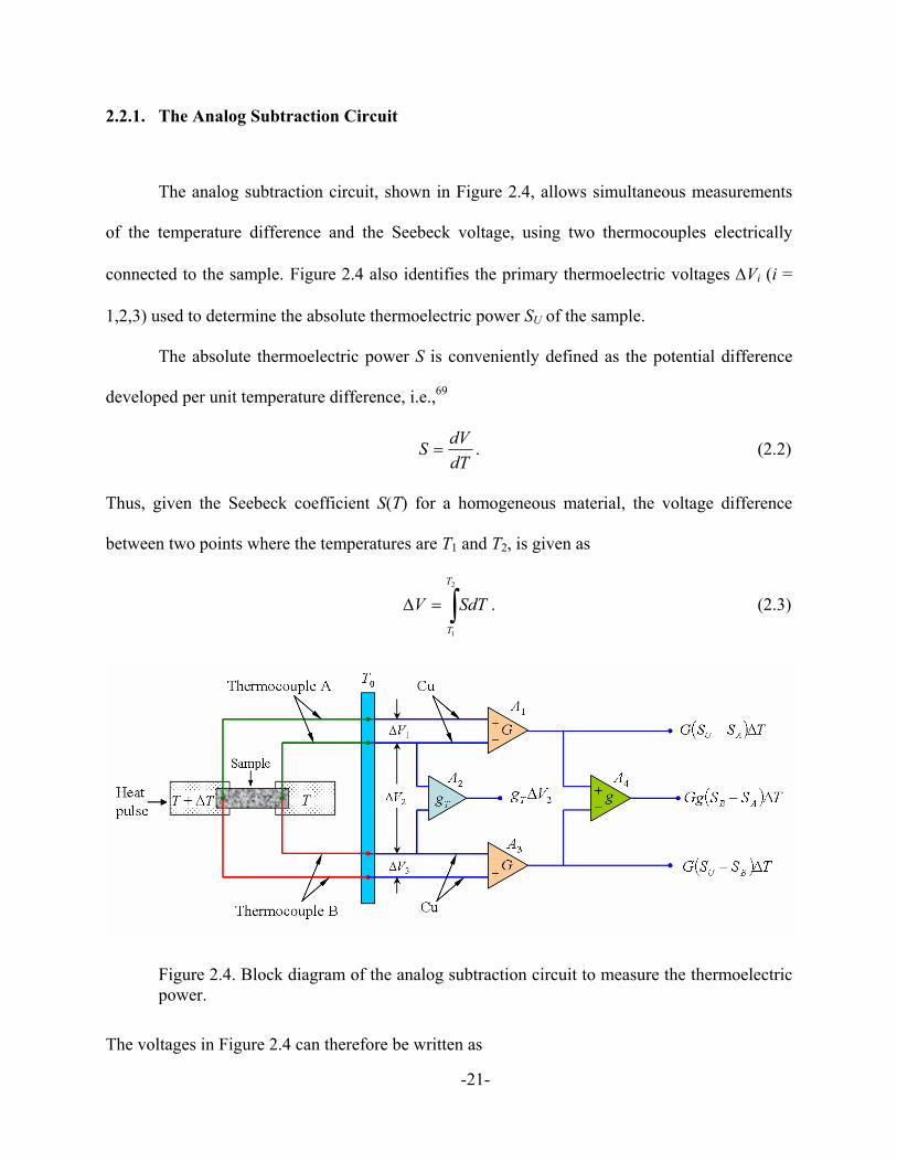
2.2.1. The Analog Subtraction Circuit
The analog subtraction circuit, shown in Figure 2.4, allows simultaneous measurements
of the temperature difference and the Seebeck voltage, using two thermocouples electrically
connected to the sample. Figure 2.4 also identifies the primary thermoelectric voltages ∆Vi (i =
1,2,3) used to determine the absolute thermoelectric power SU of the sample.
The absolute thermoelectric power S is conveniently defined as the potential difference
developed per unit temperature difference, i.e.,69
. dTdVS = (2.2)
Thus, given the Seebeck coefficient S(T) for a homogeneous material, the voltage difference
between two points where the temperatures are T1 and T2, is given as
. (2.3) 2
1
∫=∆T
T
SdTV
Figure 2.4. Block diagram of the analog subtraction circuit to measure the thermoelectric power.
The voltages in Figure 2.4 can therefore be written as
-21-

(2.4)
( ) ( ) ,
0
0
1
∫
∫ ∫ ∫∆+
∆+
∆+
∆−=−=
++=∆
TT
T
AUAU
T
T
TT
T
T
TT
AUA
TSSdTSS
dTSdTSdTSV
(2.5)
( ) ( , 0
0
0
2
TVdTSS
dTSdTSV
BA
T
T
AB
T
T
T
T
BA
=−=
+=∆
∫
∫ ∫
)
(2.6)
( ) ( ) ,
0
0
3
∫
∫ ∫ ∫∆+
∆+
∆+
∆−=−=
++=∆
TT
T
BUBU
T
T
TT
T
T
TT
BUB
TSSdTSS
dTSdTSdTSV
where ∆T is the small temperature difference between the two thermocouple junctions attached
to the sample and T0 is the reference junction temperature (~ 300 K). The thermocouples in
Figure 2.4 are thermally but not electrically anchored to the temperature reservoir at T0.
In these experiments, the voltages ∆Vi are generated by applying a small heat pulse to one
of the two ends of the sample, which establishes a time-dependent temperature difference. The
amplifiers Ai (i =1,2,3,4) respond as indicated in Figure 2.4. For small temperature differences, a
straight line should be obtained when plotting the output of A1 (or A3) versus the output of A4.
The slope is related to the sample thermopower measured relative to the conducting leads.
Taking into account the actual gains (g, G) of the amplifiers, we find
( )( ) , slope AABU SSSgS +−= (2.7)
or
( )( ) . slope BABU SSSgS +−= (2.8)
-22-

The sample temperature T is determined from an independent measurement of VAB(T). For this,
the output of A2 is polled just before the heat pulse is started, and just after it is terminated to
determine the average temperature of the sample during the measurement. The temperature
dependence of the relative thermopower of the thermocouple pair VAB(T) is previously measured
by attaching the thermocouple pair to the surface of a silicon-diode thermometer, which
determines the temperature while measuring the output of A2.
2.2.2. The Thermopower Probe
A schematic of the thermopower probe is shown in Figure 2.5. The probe consists of a
header with a hermetic multipin connector for electrical input/output, a vacuum valve, a vent
valve and a sample stage. The sample holder is fastened, using Teflon® screws, to a stainless
steel stage at the end of a 0.635 cm outer diameter, thin-walled stainless steel tube attached to the
header (the supporting tube). The supporting tube is also a gas vent line with an opening at the
lowest part of the probe. The overall probe length is 160 cm, which allows its insertion into an
ordinary liquid-helium-storage container or a tube furnace. An O-ring seals the vacuum jacket to
the header.
-23-

Figure 2.5. Schematic diagram of the thermopower and resistance measurements probe suitable for the temperature range 4-500 K.
-24-

The sample holder, shown in Figure 2.6, consists of a rectangular piece made of Macor®,
which is a white machineable ceramic. This material can be used continuously up to 1000 ºC, is
vacuum compatible (no outgassing) and provides good electrical and thermal insulation. Eight
equally spaced screws are used to provide the electrical connections. Twisted copper leads
connect the sample heater to the multipin electrical connector on the header. Similarly, twisted
thermocouple leads (0.003” diameter, Omega Engineering, Inc.) carry the thermoelectric
response to the multipin connector and from there, via copper leads, to the analog subtraction
amplifiers. Two additional copper leads (0.003” diameter, Omega Engineering, Inc.) are used to
measure the voltage during four-probe resistance measurements, as explained later in this section.
A platinum resistor (type H2104, Omega Engineering, Inc.) is thermally clamped at one end of
the sample holder and serves as the heat source.
Figure 2.6. Schematic diagram of the sample holder for the thermoelectric power and four-probe resistance measurements.
Three types of differential thermocouples could be used in our experiments: chromel-
-25-

alumel (type K), copper-constantan (type T) and chromel-gold (7 at% Fe). The thermocouple
wires (0.003” diameter, Omega Engineering, Inc.) are bonded together using a spark-bonding
technique. This is done with a device consisting of two tweezers connected, through copper
wires, to opposite polarities of a power supply set to 120 volts. The thermocouple wires are
picked up together at their bare ends with one of the tweezers, and momentarily touched with the
other tweezers. If properly held, the wires spark-bond at the junction and the sections of the
wires being held by the tweezers burn off.
The sample is mounted onto the copper heater clamp (Figure 2.6) by cementing one of
the sample ends with silver paint. Thermocouples and voltage leads for four-probe resistance
measurements also make contact with the sample via silver paint, which provides reasonably low
contact resistances especially after thermal annealing at 100 ºC. We have tried to use silver-
loaded epoxy resin, which can withstand higher temperatures and exhibits better adhesion than
silver paint, but have found that it is susceptible to cracking upon cooling. Both silver paint and
silver-loaded epoxy exhibit excellent electrical and thermal conductivity as well as
environmental resistance.
2.2.3. Experimental Setup
A schematic of the experimental setup is shown in Figure 2.7, including the computer-
interfaced system. The output from the analog subtraction circuit is sent to independent pre-
amplifiers before being collected by the computer. An IEEE-488.2 interface card and an analog-
to-digital converter (A/D) card DAS8 (Keithley MetraByte) are used for the data acquisition with
LabVIEW (National Instruments Corp.) programs. The heat-pulse generator with variable pulse
-26-

width and height is built using a micro controller (PIC 16C56, Microchip Technology, Inc.),
which can be triggered by an external TTL signal. The pulse height and duration are adjustable
in the ranges of 0-10 V and 1-20 s, respectively.
Figure 2.7. Block diagram of the system for thermoelectric power and four-probe resistance measurements instrumentation.
When the sample is at the desired stable temperature, the computer sends a TTL pulse via
one of the digital output lines of the A/D card to trigger the pulse generator. As a result, a voltage
pulse with the appropriate width and height is applied to the heater, which causes a temperature
gradient to develop and relax with time along the sample. Depending on the thermal mass of the
sample and heater block, a temperature gradient of about 0.5 K is typically developed and
relaxed over an interval of 5-20 s. After additional amplification, the thermopower data are
collected via the A/D card as ∆T increases and relaxes.
201
5
10
15
Power
ON
OFF
PULSE GENERATOR
20 0
5
1015
Voltage AOutput
BOutput
COutput
ANALOG SUBTRACTION CIRCUIT
100 1 100 1 100 1 100 1 100 1 100 1100 1100 1
Power
DC Pre-amplifiers
Pulse Generator Analog SubtractionCircuit
SourceMeter
TTL triggering signal
DAS8 A/D Board
IEEE-488.2 InterfaceBoard
4-Wire Sense
Heater
1
2
3
4
-27-

2.2.4. The Thermopower Program
Figure 2.8. The program “Thermopower Auto.vi”, showing the time evolution of the thermoelectric power of a SWNT film during vacuum-degassing at 500 K.
To measure the thermoelectric power, we created two LabVIEW (National Instruments
Corporation) programs entitled “Thermopower Auto” and “Thermopower Manual”. The
principles of operation of both programs are the same except for the fact that the former allows
us to collect data continuously, at regular intervals of time without further intervention by the
operator.
Figure 2.8 shows a sample set of thermoelectric power data as it was being taken with
“Thermopower Auto”. The program collects thermopower data at every interval of time
specified by the parameter “Data Recording”. Before each data collection, the program may be
-28-

instructed on the gain of the pre-amplifiers (Output Gain), the type of thermocouple pair used
(Thermocouple Selection), and the file where data is going to be saved (Filename). The variable
“Front Panel Connections” specifies whether the output of amplifier A1 or A3 in Figure 2.4 is
used to measure the thermopower.
A selected number of the outputs of the amplifiers A4 and A1 (or A3) are continuously
collected at a sampling rate specified by the parameter “Scan time”. When these two voltages are
plotted against each other, a straight line should be generated, which retraces itself as the
temperature difference relaxes to zero (provided the thermocouples are in good thermal contact
with the sample and are properly heat stationed), as shown in the lower left chart in Figure 2.8.
At the end of the data collection, the same data are plotted in the lower right graph, together with
a linear-least-square fitting curve. As we have discussed [Eq. (2.7)], the slope of this line is used
to deduce the sample thermoelectric power.
The upper graph in Figure 2.8 shows the thermoelectric power of a SWNT film as a
function of time, as the sample was vacuum-degassed at 500 K. The same graph in Figure 2.9
shows the thermoelectric power as a function of the temperature of a small piece of constantan,
measured according to the aforementioned method using the program “Thermopower Manual”.
The data are in good agreement with the tabulated values.
-29-

Figure 2.9. The program “Thermopower Manual.vi”, showing the temperature dependence of the thermoelectric power of constantan.
2.2.5. Calibration of the Thermocouples
The sample temperature, as well as the quantities AB SS − , , and in Eqs. (2.7) and
(2.8), is known from calibration experiments which is checked frequently. The sample
temperature is known by simply measuring the temperature dependence of the thermocouple
voltage V
AS BS
AB(T). This is done by attaching the thermocouple pair to the surface of a silicon-diode
thermometer and measuring the output voltage of amplifier A2 as a function of the temperature
determined by the silicon-diode thermometer. These data are then fitted with a polynomial
function.
-30-

The reference junction temperature T0 is needed for the calculation of the sample
temperature T. Rather than using the cumbersome ice bath (T0 = 0 ºC), T0 is measured by
thermally anchoring a type-K thermocouple to two pins on the hermetic connector of the
thermopower probe. A schematic of the connections is shown in Figure 2.10.
Figure 2.10. Schematic diagram of the connections to A2 amplifier to measure the sample temperature (top) and the equivalent circuit (bottom).
The junctions J2 and J3 and the thermocouple (or thermistor) are all assumed to be at the
same temperature T0. We can easily show, using Eq. (2.2), that the output voltage ∆V2 is
proportional to the temperature difference (T – T0). Usage of an ice bath at the reference junction
allows one to determine the temperature directly from a ∆V2 versus T calibration curve. If T
needs to be known to higher accuracy, perhaps a secondary thermometer such as a silicon diode
-31-

should be used. Although slow temperature drifts in room temperature T0 could cause some error
in absolute temperature, they are too slow to affect measurements of the thermopower, because
each data point is collected during a short period of time (~ 20 s).
-1.25
-1.00
-0.75
-0.50
-0.25
0.00
0.25
g T∆V 2 (
V)
300250200150100500T (K)
30
25
20
15
10
5
0
(SK
P – S
Au:
Fe) (
µV/K
)300250200150100500
T (K)
Figure 2.11. The output voltage of amplifier A2 as a function of the sample temperature (left) and the temperature dependence of the relative thermoelectric power of a chromel-Au:Fe thermocouple pair (right).
According to Eq. (2.5), the temperature-dependent relative thermopower of the
thermocouple pair is given by the relation
. dT
dVSS BA
AB =− (2.9)
Therefore, by simply evaluating the derivative of the ∆V2 versus T calibration curve, we can
determine the temperature dependence of AB SS − . Figure 2.11 shows the temperature
dependence of the output voltage ∆V2 of the thermocouple amplifier A2 and the temperature
derivative of that calibration curve for a chromel-Au:Fe thermocouple pair ( ) . Fe:AuKP SS −
The absolute thermopower of an unknown sample is obtained from either Eq. (2.7) or
(2.8) by using calibration data for SA(T) or SB(T) with respect to copper. These quantities are
determined by simply using a piece of high-purity copper as the sample. Figure 2.12 shows the
-32-

relative thermopower data of chromel ( )CuKP SS − and Au:Fe ( )Fe:AuCu SS − with respect to
copper, measured according to the aforementioned method. Finally, tabulated values for the
thermopower of copper are used to obtain absolute thermoelectric power values.
20
15
10
5
0
S (µ
V/K
)
300250200150100500T (K)
SKP – SCu
SCu – SAu:Fe
Figure 2.12. Temperature dependence of the thermoelectric power of chromel and gold:iron alloy with respect to copper. The solid lines represent polynomial fits to the data.
2.3. Four-Probe Resistance Measurements
To measure the resistance of our samples the four-probe method was employed. This is a
very versatile means, used widely in physics, for the investigation of electrical phenomena.
Resistance measurements in the normal range (> 1 kΩ) are generally made using the two-probe
-33-

method. Here, a test current is forced through two test leads and the resistance being measured.
Then, the voltmeter measures the voltage across the resistance through the same set of test leads
and computes the resistance accordingly. The main problem with the two-probe method,
particularly for samples of low resistance, is that one inadvertently also measures the contact
resistance of the wires to the sample. Since the test current causes a small, but significant,
voltage drop across the contact resistances, the voltage measured by the meter will not be exactly
the same as the voltage directly across the test resistance and considerable error can result. For
example, one ohm of cable and contact resistance in a conventional two-probe circuit adds a
0.1% error to the 1-kΩ measurement. When one is measuring a very small resistance, especially
under variable temperature conditions, the contact resistance can dominate and completely
obscure changes in the resistance of the sample itself. This is the situation that exists for SWNT
networks.
The effect of cabling and contact resistances, as well as other series resistance errors, can
be eliminated with the use of a four-probe method, often called a Kelvin measurement. A
schematic of a four-probe connection, as well as the experimental arrangement, is shown in
Figure 2.7. In this method, four wires attached to the sample are used for resistance
measurements. A constant current is made to flow along the length of the sample through one set
of test leads (probes labeled 1 and 4 in the figure), while the voltage across the sample is
measured through a second set of leads called sense leads (probes labeled 2 and 3 in the figure).
In our case, one arm of each thermocouple is used as the current lead.
Although some small current may flow through the sense leads, it is usually negligible
(typically pA or less) and can generally be ignored for all practical purposes. Since the voltage
drop across the sense leads is negligible, the voltage measured by the meter is essentially the
-34-

same as the voltage across the sample. Consequently, the resistance value can be determined
much more accurately than with the two-probe method.
Figure 2.13. The program “DC 4-Probe Resistance.vi” showing the resistance as a function of temperature for a SWNT mat.
A SourceMeter 2400 (Keithley Instruments, Inc.) was used to provide a constant current
to the experiment and measure the voltage. This instrument combines a precise, low-noise,
highly stable DC power supply with a low-noise, highly repeatable, high-impedance multimeter.
To cancel thermal emf, the current reversal algorithm is employed. That is, two measurements
with currents of opposite polarity are programmed. Then, the two measurements are combined to
eliminate unwanted offsets.
Data acquisition is carried out remotely via an IEEE-488.2 connection with a computer as
shown in Figure 2.7. For this purpose, we created a LabVIEW program entitled “DC 4-Probe
-35-

Resistance”, shown in Figure 2.13. The program collects sample and thermocouple voltages
either continuously at a specified rate (Scan rate) or at the user command from the front panel.
After colleting a specified number of data points (No. Samples), the program plots the calculated
sample’s resistance versus temperature or time (Type of Measurement).
The variables under “Control Settings” specify the methods used to measure resistance
with the Keithley SourceMeter 2400. The program allows four-probe and two-probe resistance
measurements. The offset-compensation method cancels out unwanted offset in the voltage and
current readings by measuring resistance at the specific source level, and then subtracts a
resistance measurement made with the source set to zero. Temperature changes across
components within the instrument can cause the reference and zero values for the A/D converter
of the SourceMeter to drift due to thermoelectric effects. Auto zero acts to negate the effects of
drift in order to maintain measurement accuracy over time. Without auto zero enabled,
measurements can drift and become erroneous. Note that auto zero and offset-compensation
measurements are additional corrections to the one obtained by using the current reversal
algorithm, but the use of all these correction procedures simultaneously will decrease the
measurement speed. Control display command is used to enable and disable the front panel
display circuitry of the SourceMeter. When disabled, the instrument operates at a higher speed.
The variables under “Power Source Parameters” allow the configuration of the current
source. The operator can set the current level (I-Source), the limit voltage (V-compliance),
auto/manual range for voltage measurements (V-AutoRange), the range for manual current (I-
range) and voltage (V-range) measurements.
Before each data collection, the program may also be instructed on the type of
thermocouple pair used to measure the temperature (Thermocouple Selection) and the file where
-36-

data is going to be saved (Filename).
2.4. Gas/Chemical Adsorption Measurements
Figure 2.14. Schematic diagram of the gas handling system for gas/chemical adsorption experiments.
For gas adsorption measurements, a gas handling system is attached to the vent valve of
the thermopower probe. The basic components are shown in Figure 2.14. This system consists of
an oxygen/moisture trap (OT-4-SS, R&D Separations, Inc.), capable of reducing the oxygen and
moisture content of a gas stream to less than 20 ppb; a general purpose differential capacitance
manometer (Baratron 221, MKS Instruments, Inc.), a vacuum valve and a vent valve. Before
admitting the gas into the thermopower probe, the gas handling system is properly evacuated and
leak checked through the vacuum valve. An ultra-high purity grade gas cylinder is connected to
the vent valve of the gas handling system for gas adsorption experiments. If needed, a side arm
attached to a glass bulb containing a spectral grade liquid chemical (Sigma-Aldrich, Co.) is
-37-

connected to the vent valve of the gas handling system for chemical adsorption studies.
-38-

Chapter 3.
Thermoelectric Power of Single-Walled Carbon Nanotubes
3.1. Seebeck Effect: Theory
The Seebeck effect, depicted schematically in Figure 3.1, is the open-circuit (zero
current) voltage response to a temperature gradient in a material. This phenomenon was
discovered in 1821 by the German physicist Thomas Johann Seebeck who observed that a
voltage (electromotive force, emf) was developed in a loop containing two dissimilar metals,
labeled A and B in Figure 3.1(a), provided that the two junctions c and d were maintained at
different temperatures.69,70 The voltage across the loop was found to depend on the type of
metals used and the temperature of the junctions.
Physically, the phenomenon arises in a single material [Figure 3.1(b)] because the
electrons at the hot end of such a conductor can find states of lower energy at the cold end,
towards which they diffuse. This diffusion current is accompanied by the accumulation of extra
electrons at the cold end, setting up an electric field or a potential difference between the two
ends of the material. The electric field builds up until a state of dynamic equilibrium is
established between electrons rushing down the temperature gradient and those moving against
the gradient due to the electrostatic field. This thermoelectric effect is sometimes referred to as
the “diffusion thermoelectric power”.
-39-

Figure 3.1. (a) Basic thermoelectric open circuit that displays the Seebeck effect. (b) The Seebeck effect: A temperature gradient along a conductor gives rise to a potential difference.
The Seebeck coefficient, thermoelectric power or simply thermopower S is the ratio of
the open-circuit voltage developed ∆V to the temperature difference ∆T:
. lim0 T
VST ∆
∆=
→∆ (3.1)
Almost all the theoretical treatments of thermoelectric power in macroscopic systems are
based on the Boltzmann transport equation, from which the following expression for the
thermopower can be derived:71
[ ]
,)()()(
)()()()(1
)(
)(
∫∫
ε=ε
ε=ε
⎟⎠⎞
⎜⎝⎛
ε∂∂
τ
⎟⎠⎞
⎜⎝⎛
ε∂∂
−ετ
=
k
k
kvkvkk
kkvkvkk
fd
fEd
eTS
F
(3.2)
where τ is the electron relaxation time, v is the electron group velocity, e is the electronic charge,
-40-

f is the equilibrium distribution function of the electrons, ε is the energy of the electron relative
to the chemical potential EF, and the integral is taken over all momentum states k. Note that the
thermoelectric power is related to the energy carried by the electrons per unit charge, which is a
function of the relative contribution of the electron to the total conduction. The sign of the
thermopower is determined by whether the dominant conduction takes place in states above, or
below, the chemical potential EF.
For a degenerate metallic conductor, a calculation based on Eq. (3.2) (see Appendix A)
leads to the following expression for the diffusion thermopower:
( ) , ln3
F
22
ATdE
Ede
TkSEE
B ≡⎟⎠⎞
⎜⎝⎛ σπ
−==
(3.3)
where σ(E) is the conductivity that would be found in a metal for electrons of energy E, given by
the well known relation
( ) ( ) ( ) ( ). 22 EENEeE τυ=σ (3.4)
Here N(E) is the density of states, and υ(E) and τ(E) are, respectively, the free carrier velocity
and relaxation time at energy E. For an electron-like band, the thermopower is negative, while
for a hole-like band the thermopower is positive.
The energy dependence of the relaxation time is often written as
, (3.5) )( mEE β=τ
where β is a constant and m a number that depends on the type of scattering that is dominant.
Consequently, it is easily shown that in the free-electron approximation Eq. (3.3) reduces to
, 23
3 F
22
⎟⎠⎞
⎜⎝⎛ +
π−= m
EeTkS B (3.6)
which indicates that S is expected to vary linearly with temperature. Elementary calculations71
-41-

predict that m = 3/2 in the temperature range where the relaxation time is limited primarily by
electron-phonon scattering, and m = – 1/2 at very low temperatures where τ(E) is limited by
impurity scattering. Hence, a change in the slope dTdS as the temperature is reduced would be
expected in the free-electron approximation, i.e.
region) resistance (residual low very 22
TEe
TkSF
Bπ−= (3.7)
region) scattering(phonon high 3
22
TEeTkSF
Bπ−= (3.8)
The thermopower of semiconductors with relatively few conduction electrons (non-
degenerate semiconductors) shows temperature dependence different from that found in metals.
In the case of semiconductors, one has to replace the Fermi-Dirac statistics in Eq. (3.2) by the
Boltzmann statistics, in which case one obtains
, for Fcc
B
cB EEATkEE
ek
S >⎥⎦
⎤⎢⎣
⎡+
−= (3.9)
, for Fvv
B
vB EEATkEE
ek
S <⎥⎦
⎤⎢⎣
⎡+
−= (3.10)
where Ac and Av are temperature-independent constants. In general, the thermoelectric power for
a non-degenerate semiconductor is of the form
, ⎥⎦
⎤⎢⎣
⎡β+
λ=
TekS B (3.11)
where λ is the gap temperature measured from the midgap to the band edge and β is a constant. β
= 3 when both the density of states and the mobility increase linearly with E. β = 1 for constant
density of states and mobility.72 Using the energy dependence of the relaxation time in Eq. (3.5),
m−=β 25 .73
-42-

Thus, in contrast to the linear temperature dependence observed in metals, a
semiconductor should exhibit a thermoelectric power which is proportional to the reciprocal of
temperature. In addition, the thermoelectric power of a semiconductor is usually large at room
temperature (in the mV/K range). Metals, on the other hand, usually display a small
thermoelectric power (in the order of a few µV/K).69
In recent years, there has been increasing interest in the thermoelectric phenomena in
carbon nanotubes. Thermoelectricity has been shown to be a valuable and effective probe of
electronic structures, and a suitable tool for understanding the scattering dynamics of electrons
and phonons and the electron-phonon interactions in solids.
3.2. Thermoelectric Power of Carbon Nanotubes: Background
Figure 3.2 shows a typical temperature dependence of the thermoelectric power for an
“as-prepared” SWNT mat. The thermoelectric power data is in reasonably good agreement with
the earliest results,74-76 which yielded surprising results: at high temperatures the thermoelectric
power has a large positive value (i.e., S ~ 40-60 µV/K at 300 K, depending on the sample
history) that decreases monotonically with decreasing temperature, while at low temperatures the
thermoelectric power is quasi-linear in temperature and rapidly approaches zero as T → 0. There
is also a strong non-linearity in the range ~ 80-100 K, either in the form of a superimposed
“knee” (change of slope) or a more pronounced “bump” or peak.
The temperature dependence of the thermoelectric power of SWNT bundles is unusual; it
does not correspond to that of a simple metal or semiconductor. However, a metallic behavior
could be incorporated at low temperatures (below ~ 100 K), or by considering an extension of
-43-

the linear section at very low temperature (below 50 K) as shown, respectively, by the curves (a)
and (b) in Figure 3.2.
This behavior is in sharp contrast with the thermoelectric power observed for the basal
plane of graphite which exhibits a small value for the thermoelectric power (S = – 4 µV/K at 300
K) and nearly linear temperature dependence.77 Graphite has a pair of weakly overlapping
electron and hole π bands with near mirror symmetry about the Fermi level. Approximately
equal numbers of electrons and holes in these symmetric π bands are consistent with the small
(negative) linear thermoelectric power observed below room temperature.
40
30
20
10
0
S (µ
V/K
)
300250200150100500T (K)
(a)
(b)
Figure 3.2. Temperature dependence of the thermoelectric power for an air-saturated SWNT mat. The solid line is a guide to the eye. The dashed lines (a) and (b) represent the ways in which metallic behavior could be incorporated in the thermoelectric behavior of SWNTs.
-44-

Based on the fact that the sign of the thermoelectric power is always positive in the
measuring temperature range, it was implied that the majority charge carriers in the carbon
nanotubes should be p-type, and the hole carriers are dominant. The large magnitude of the
thermoelectric power is surprising because metallic tubes are predicted to have electron-hole
symmetry and hence, a thermoelectric power close to zero. The obtained temperature
dependence of the thermoelectric power is also unusual, and cannot be simply explained by a
single-band model for a metal [Eq. (3.3)] or a non-degenerate semiconductor [Eq. (3.11)], over
the studied temperature range. Numerous models, however, have been proposed to explain this
complicated behavior, including parallel metallic and semiconducting pathways,74,78 variable-
range hopping,78 electron-phonon enhancement,78 fluctuation-induced tunneling,79 and Kondo
effect.76 More complicated heterogeneous models have also been considered.80 We discuss next
the merits and difficulties of some of these approaches.
3.2.1. Parallel Heterogeneous Model of Metallic and Semiconducting Pathways
The observed temperature dependence of the thermoelectric power for SWNT mats
suggests a parallel heterogeneous model of metallic and semiconducting nanotubes within the
ropes.74,78 In principle, since a nanotube bundle consists of various nanotubes, the total
thermoelectric power should result from the combination of the contributions from all nanotubes
with different (n,m). For two types of parallel conductors (metallic and semiconducting), we can
write the total thermopower S as a weighted average
,ss
mm S
GGS
GGS += (3.12)
where Sm and Ss are the thermopower of the metallic and semiconducting tubes, respectively, Gm
-45-

and Gs are the corresponding electrical conductances, and G is the total conductance of the rope.
To derive Eq. (3.12) let us consider the situation shown in Figure 3.3. From Eq. (3.1), the
open-circuit potential difference produced across conductor a alone would be given by
, and similarly TSV aa ∆=∆ TSV bb ∆=∆ for conductor b acting alone. It then follows from
simple circuit theory that the resultant open-circuit voltage produced by the two conductors in
parallel is given by an expression similar to Eq. (3.12). This circuit theorem is sometimes known
as the “ladder” theorem.
Figure 3.3. Illustration of the combination of thermoelectric powers for conductors in parallel (also applicable to the two-band model).
The conductance from the metallic tubes is expected to be proportional to the reciprocal
of temperature, i.e., TGm 1∝ , at least at high temperatures. Assuming an activated form for the
semiconducting conductance, ( )TGs λ−∝ exp , and that the total conductance is dominated by
the metallic tubes, then from Eqs. (3.3) and (3.11), the total thermopower is74
,exp)( ⎟⎠⎞
⎜⎝⎛ λ−+λ+=
TCTBATS (3.13)
where A, B, and C are constants. The solid line in Figure 3.4 represents our fit of Eq. (3.13) to
our data set shown in Figure 3.2. Even though this model provides a reasonably good fit to the
-46-

thermoelectric power data, the fitting parameters are less than satisfactory in several respects.74
The fitted thermoelectric power for a mat of SWNTs is seen to be dominated by the first
term in Eq. (3.13), where the positive value of the temperature coefficient A implies a
thermoelectric power contributed by the holes of metallic nanotubes, with a room temperature
magnitude of S ~ 80 µV/K. In general, the model predicts an unphysically large magnitude of
the diffusion thermoelectric power for the metallic tubes (Sm ~ 80-200 µV/K at 300 K).78
40
30
20
10
0
S (µ
V/K
)
300250200150100500T (K)
A = 0.249 µV/K2
B = -0.668 µV/K2
C = 0.486 µV/K2
λ = 521 K
Figure 3.4. Fits to measured thermoelectric power of a SWNT mat using a parallel heterogeneous model of semiconducting and metallic tubes. The solid line represents a fit to the data using Eq.(3.13). Fitting parameters extracted from our fit are also shown in the figure.
The negative term would presumably be contributed by the electrons of the conduction
band for the semiconducting nanotubes. Therefore, within this model, the measured magnitude
-47-

of the temperature-dependent thermoelectric power is due to a near cancellation of very large
metallic and semiconducting thermopowers of opposite sign; a situation regarded as unlikely.
The value of semiconducting tube energy gap, obtained from the parameter λ, is ~ 0.09
eV. Previous studies have found values of 10-20 meV, which are significantly smaller than
values expected for the energy gap. In general, the energy gap of a semiconducting nanotube is
expected to vary from 0.5 eV to a few eV in the diameter range 1 nm < d < 2 nm, depending
upon the geometry.51,81 The mean tube diameter measured for the sample whose data appear in
Figure 3.4 is ~ 1.4 nm. This model consequently predicts very small semiconducting gaps and
conductances that are considerably larger than typical observations.82,83 Moreover, the model
with metallic and semiconducting conduction in parallel cannot by itself account for the
resistivity behavior, because the semiconductor contribution to conductivity is frozen out at
lower temperatures where it is observed experimentally.
3.2.2. Variable-Range Hopping
An alternative parallel tube model was proposed where metallic conduction is in parallel
with disordered semiconductor conduction via 3D variable-range hopping.78 For conduction by
variable-range hopping, the expected thermopower (which is positive for hole conduction) is
given by84
( ) ( ) , ln2
F
21
0
2
EE
B
dEENdTT
ek
S=
⎥⎦⎤
⎢⎣⎡= (3.14)
where N(E) is the density of states at the Fermi level and T0 is the parameter appearing in the
Mott variable-range hopping law of conduction:
-48-

, exp4
1
00
⎥⎥⎦
⎤
⎢⎢⎣
⎡⎟⎠⎞
⎜⎝⎛−=
TT
GG (3.15)
G0 is usually considered to be weakly dependent on temperature.
Using Eq. (3.12) one now obtains
. exp4
1
21 0
⎥⎥⎦
⎤
⎢⎢⎣
⎡⎟⎠⎞
⎜⎝⎛−+=
TT
BTATS (3.16)
40
30
20
10
0
S (µ
V/K
)
300250200150100500T (K)
A = -0.423 µV/K2
B = 31.54 µV/K3/2
T0 = 636 K
Figure 3.5. Fits to measured thermoelectric power of a SWNT mat using a parallel heterogeneous model of disordered semiconducting and metallic tubes. The solid line represents a fit to the data using Eq. (3.16). Fitting parameters extracted from the fit are also shown in the figure.
As shown in Figure 3.5, this expression does not provide a reasonable fit to the observed
thermoelectric power (Figure 3.2), as the predicted change in slope is smoother than that
-49-

predicted. The model also gives an even larger metallic contribution when fitted to the data. On
the other hand, the simple combination of metallic and hopping conduction regions suggested by
the resistivity behavior of SWNTs fails to provide reasonable fitting to both the resistivity and
the thermopower using the same set of parameters; mainly T0.
3.2.3. Electron-Phonon Enhancement
The quasi-linear temperature dependence of the thermoelectric power in a metal can be
understood by the electron-phonon enhancement effect.78,85 The enhancement of the linear
temperature dependence of metallic thermoelectric power can be expressed as
[ ] ,)(1 ATTS Sλ+= (3.17)
where λS(T) denotes the temperature dependent enhancement from the coupling of the electrons
and phonons and A is the coefficient of diffusive thermoelectric power.
The fits to the thermoelectric power data using Eq. (3.17) give the reduction of slope
above ~ 100 K. However, the values of the effective enhancement λS(0) are as large as those
expected for good superconductors.78 Since nanotubes have not been observed to superconduct at
temperatures as low as 1.5 K, a very large value for λ seems inappropriate.
3.2.4. Fluctuation-Assisted Tunneling
A SWNT network can be assumed to contain many metallic regions separated by small
insulating barriers (for example, due to poor connectivity between individual nanotubes). The
contact resistance of these barriers can dominate the overall resistance of the system. Such
-50-

systems can be described phenomenologically by Sheng’s theory of fluctuation-induced
tunneling.86 According to this theory, the electrical conductivity is given by the relation
. exp0
10 ⎟⎟
⎠
⎞⎜⎜⎝
⎛+
−σ=σTT
T (3.18)
The thermoelectric power can also be calculated from this theory.79 The contribution to
the thermoelectric power would be weighted by the fraction of the temperature difference
appearing across the barriers compared to that appearing across the metallic portions.
This model can describe the thermoelectric power data of SWNTs reasonably well and a
knee, such as that occurring in the thermopower data at ~ 100 K, is predicted by this theory.
However, additional contributions to the thermoelectric power must be considered in order to
achieve the positive curvature seen in the data for T ≥ 100 K.
3.2.5. Kondo Effect
An anomalously large peak superimposed on the metallic thermopower has been
observed in the range 80-100 K in some transition-metal doped SWNT mats, and has been
tentatively attributed to a Kondo anomaly associated with the residual (magnetic) catalyst
residing as particles on the bundles or rope surface, or trapped as atoms or small clusters within
the bundles.76 In other materials, the interaction between the magnetic moments of the impurity
atoms and the spin of the conduction electrons has been shown to lead to a new spin-dependent
scattering mechanism and a narrow hybridization peak or “Kondo resonance” in the electronic
density of states positioned near the Fermi level.87
The Kondo mechanism was also suggested because the particular catalyst caused a
-51-

concomitant change in the strength of the upturn in the electrical resistivity with decreasing
temperature below ~ 100 K. Further support for this argument is that the chemical treatment of
the SWNT samples with iodine, significantly reduces the Kondo contribution.76 The drawback in
the Kondo proposition to explain the thermoelectric power of SWNTs is that the thermoelectric
power peak should occur at BK kETT ∆≈= , where ∆E is the width of the Kondo resonance
near the Fermi level. One might expect a stronger variation in TK with various magnetic
impurities (e.g., Fe, Ni, Co), unless the effect is associated with Y, which is a common element
in all of the catalysts considered in that study.
3.2.6. Thermoelectric Power of Oxidized SWNT Networks
Recent experimental studies88,89 have reported that the measured SWNT electronic
properties (including the thermoelectric power and the electrical resistance) are extremely
sensitive to the presence of molecular oxygen in the nanotube. Specifically, it has been found
that, at room temperature, the resistance changes by 10-15% when SWNT mats are cycled
between vacuum and air exposure. In addition, after exposure for ~ 2-3 h under ambient
conditions to room air, SWNTs were found to acquire thermopower values unusually large
compared to those of ordinary metals and graphite. Most strikingly, it was reported that some
small-gap semiconducting nanotubes exhibit metallic behavior when they are exposed to
oxygen.90
Our in situ measurements while heating these O2-doped samples in a ~ 10-7 Torr vacuum
at ~ 500 K (i.e., to remove the adsorbed O2) showed that the large positive thermopower
identified with O2 doping first decreases with time and then changes sign, with the fully degassed
-52-

sample finally exhibiting a large negative thermopower after 10-15 h. These results were
interpreted as due to the formation of a charge transfer complex . For the
semiconducting tubes, the position of the Fermi level must shift toward the valence band. This
will be discussed in detail in the following section.
δ−δ+ − 2OC p
-40
-30
-20
-10
0
10
20
30
40
S (µ
V/K
)
300250200150100500T (K)
Air-saturated
Degassed @ 500 Kin vacuum
Figure 3.6. The temperature dependence of the thermoelectric power for an “as-prepared” SWNT mat in its air-saturated and degassed states. The solid lines are guides to the eye.
Figure 3.6 shows our S(T) data for the same SWNT sample for two cases: air-saturated
and degassed states. For the air-saturated sample, the thermoelectric power is always positive
and approaches smoothly S = 0 as T → 0, from a large value S ~ 40 µV/K at 300 K. For the
sample degassed at 500 K for 24 h in a ∼ 10-7 Torr vacuum, the thermoelectric power is negative
over the entire temperature range 4 K < T < 300 K, with a room temperature magnitude
-53-

comparable to that measured under air-saturated condition. As can be seen, the functional forms
of S(T) for air-saturated and degassed samples appear to be almost “mirror images” of each other,
reflected about the horizontal temperature axis. The results in Figure 3.6 demonstrate that the
previously published large positive thermoelectric power data should not be considered as an
intrinsic SWNT behavior, but rather the result of various degrees of oxygen doping.
The interactions of O2 with carbon nanotubes have been investigated in several recent
theoretical studies.91-103 According to the results, there are three different pathways for oxygen
adsorption on SWNTs:
(a) Molecular oxygen (in its spin-triplet ground state) physisorbs on the outer surface of a perfect
tube wall with relatively small binding energies up to 0.25 eV, accompanied by a small charge
transfer of ≤ 0.1 electron from the carbon nanotube to the O2 molecule. There may be no barrier
for O2 physisorption onto perfect carbon nanotubes.101 On the basis of the calculated density of
states, it was also suggested that the adsorbed O2 molecules can dope the semiconducting
nanotubes with hole carriers and that conducting states are present near the band gap.92
(b) Molecular oxygen (in its spin-singlet excited state) exothermically chemisorbs to the tube
wall through an intermediate cycloaddition step to give two spatially well-separated epoxide
groups or two single C−O bonds, with significant charge transfer from the nanotubes to the O2
molecules.94,97,99,103 The adsorption is high (~ 0.34 eV) and the activation barrier can be as low as
~ 0.6 eV, which is accessible at room temperature.97 O2 molecules can be excited into a more
reactive spin-singlet state by UV-light,100 sunlight, photosynthesizers (e.g., fullerene
impurities),97 or by topological defects.101 In addition, adsorption at defect and impurity sites
may help overcome the kinetic activation barrier.100,101
(c) Molecular oxygen diffuses to the edge of open tubes where it dissociatively chemisorbs with
-54-

an adsorption energy of up to 8.4 eV to form strong C−O bonds, even without any activation
barrier.93
3.3. Thermoelectric Power of SWNT Films
Here we present the results of a systematic study on a purified thin film of tangled SWNT
ropes, which show that the thermoelectric power is determined by coordinated effects in both the
semiconducting and the metallic tubes. However, the thermoelectric power will be shown to be
dominated by the metallic tubes in the ropes. The sign and magnitude of the thermoelectric
power will be shown to be determined by the relative concentrations of (acceptor state; δ =
fractional charge) and an unidentified donor state in the semiconducting tubes, possibly due to
wall defects. In fact, we show that a fully compensated sample can exhibit a thermopower S ~ 0
over a wide temperature range (4 < T < 500 K). In the compensated case, we will argue that the
Fermi level for a rope containing semiconducting and metallic tubes is very near the intrinsic
position. Furthermore, in this case, the mirror symmetry of the metallic band structure makes
offsetting contributions from electrons and holes. In contrast to this view, Avouris and co-
workers
δ−2O
104-106 have demonstrated a similar behavior using SWNT field effect transistors (CNT-
FET), i.e., the p-type electronic character can be turned into a fully n-type one by simply
annealing in vacuum. Based on the observation that oxygen treatment has no effect on the
threshold voltage for turning on a CNT-FET, they argued that barriers at the metal-
semiconducting contact control the carrier injection even though bulk doping may take place.
According to Avouris and co-workers,104-106 the dependence of these barriers on oxygen
determines the electrical character of the CNT-FET. It may be that the nanotubes in the CNT-
-55-

FET studied were defect-free and contained only weakly interacting (physisorbed) oxygen. In
contrast, our samples contained sufficient defect density that could bind strongly with O2
involving charge transfer.
Despite the numerous theoretical and experimental investigations, the microscopic
mechanism responsible for the observed changes in the electronic-transport properties of SWNTs
is still discussed controversially. The sensitivity of carbon nanotubes to O2 exposure is an
important issue, as it raises questions about the stability of devices made of carbon nanotubes
upon air exposure. On the other hand, the observed effect of oxygen exposure on the properties
of carbon nanotubes raises the possibility that unintentional oxygen contamination during
preparation of nanotubes samples might have led to incorrect analysis of the experimental data.90
3.3.1. Role of Contact Barriers on the Transport Properties of SWNTs
It has been argued79,80 that the measured thermoelectric power of a SWNT network may
be affected by rope-rope contacts and other barriers (e.g., defects, tube-tube contacts, etc.) in the
SWNT mat or film and their random orientations relative to the thermal gradient. This is a
reasonable concern, particularly if we note that a SWNT network consists of ropes, themselves
containing metallic and semiconducting tubes that may be loosely touching each other through
semiconducting tubes and/or amorphous carbon on the rope surface, not eliminated by the
purification process (Figure 3.7).
-56-

Figure 3.7. Sketch of crystalline SWNT ropes, where fibrillar carbon nanotubes are separated by disordered regions (Adapted from Kaiser et al.107)
In this picture, the thermoelectric power could be the result of a pathway of
semiconducting tubes broken by series-connected inter-tube barriers, where the thermopower
due to the insulating barriers could be described by either an activated hopping-like conduction
model80 or a fluctuation-induced tunneling model.79 We investigated the possible influence of
rope-rope contacts on the four-probe resistance [Figure 3.8(a)] and the thermoelectric power
[Figure 3.8(b)] on film or mat samples by observing the change in these quantities under the
action of uniaxial stress.
The experimental geometry is shown schematically in the inset to Figure 3.8(b). The
measurements were made in air at T ~ 300 K as a function of the loading force F applied normal
to the substrate supporting the SWNT mat. Thermocouples [TC(1), TC(2)] and voltage leads
[V(1), V(2)] made contact with the SWNT mat via silver epoxy outside the region of applied
stress. The pressure was calculated directly form the cross-sectional surface area of the insulating
rod and the weights placed on top of it.
-57-

1.00
0.95
0.90
0.85
0.80
R/R 0
1.81.51.20.90.60.30.0Pressure (MPa)
(a)70
60
50
40
30
S (µ
V/K
)
1.81.51.20.90.60.30.0Pressure (MPa)
F
V(1) V(2)
TC(1) TC(2)
F
V(1) V(2)
TC(1) TC(2)
(b)
Figure 3.8. Uniaxial pressure dependence of (a) the normalized room temperature resistance R/R0 and (b) the thermopower S for two different “as-prepared” SWNT mats. The inset shows the experimental geometry where the applied force F is perpendicular to the sample.108
As can be seen in Figure 3.8, the applied force (stress) impacts the four-probe resistance
but not the thermopower. It should be noted that the data are for two O2-doped samples under
ambient conditions. If the contact regions among the ropes dominated the thermopower, when
these regions become better heat conductors under the applied stress, the thermopower might be
expected to decrease. However, as shown in Figure 3.8(b), the pressure has little effect on the
thermopower. The insensitivity of S to the improved rope-rope contact resistance, observed via
the decreasing R in Figure 3.8(a), is taken as direct evidence that the contact barrier between
ropes is not significantly involved in the thermoelectric power of the SWNT sample. This is
consistent with the measurement of the thermoelectric power under “open-circuit” (zero current)
conditions.
3.3.2. Effect of Oxygen Doping on the Thermoelectric Power of SWNTs
Figure 3.9 shows the time evolution of the thermoelectric power at T = 500 K for a
-58-

typical purified SWNT thin film sample under vacuum. The SWNT sample was previously
exposed to air under ambient conditions for several days, then mounted in the measurement
apparatus, evacuated to ~ 10-7 Torr and heated from 300 to 500 K. At point A, the sample is still
nearly air-saturated which was accomplished under ambient conditions.
30
20
10
0
-10
S (µ
V/K
)
121086420Time (h)
O2 desorption
O2 adsorption
T = 500 K
(A)
(B)
(D)
(C)
Figure 3.9. Thermopower response to vacuum and O2 (1 atm) at T = 500 K. (A → C): Vacuum-degassing of a sample initially O2-doped under ambient conditions for several days. (C → D): Exposure of the degassed sample to 1 atm of O2 established at C.108
As the sample was degassed at T = 500 K in a vacuum of ∼ 10-7 Torr, the thermopower
was observed to decrease slowly from an initial value S = 8 µV/K, change sign at B (fully
compensated state), and then gradually approach a constant value of S0 = – 10 µV/K near C
(fully degassed state). The observed thermoelectric behavior at T = 500 K in vacuum is in
agreement with previously reported results on similar samples.88,89 However, very recently,
-59-

Goldoni et al.109 have used high resolution core-level photoemission spectroscopy to study the
interaction between O2 and SWNTs at low temperature (150 K). A strong interaction with O2
was found for samples contaminated with traces of Na (mainly chemical residues of the
purification, dispersion, and filtration processes) due to charge transfer from the tube to the
Na−O complex, whereas weak interaction with O2 was observed when dosing the Na-free sample.
Thus, Goldoni et al.109 suggested that O2 molecules have no effect on the transport properties of
SWNTs if impurities (i.e., catalyst particles, contaminants and defects coming from the chemical
treatments) are carefully removed from the nanotube samples. Note that, in our purification
procedure, we do not use surfactants or NaOH, which might leave residual Na in the SWNTs.
Besides, as mentioned in Ref. 109, the high-T annealing at ultrahigh-vacuum completely
removes any Na contamination and strongly reduces the number of defects introduced by the
purification treatments, restoring the nanotube structure and the bundle network. Our samples
were annealed at ~ 1200 ºC in a ∼ 10-7 Torr vacuum for 24 h. We also note that the experiments
in Ref. 109 have been carried out by exposing nanotubes to O2 at 150 K. At this low temperature,
we expect O2 to interact weakly with SWNTs through a physisorption process only. Due to the
negligible charge transfer between physisorbed oxygen and SWNTs, such O2 species are not
expected to facilitate the doping responsible for the observed change in the transport properties
of SWNTs.110 As suggested by Ulbricht et al.,110 based on thermal desorption experiments and
molecular mechanics calculations, it seems likely that the observed effect of O2 on the transport
properties of SWNTs is predominantly due to charge transfer by minority oxygen species,
weakly bound either at defect sites on the SWNT bundles or at tube-metal contacts in electronic
devices.104-106
Exposure of the fully degassed film to 1 atm overpressure of pure oxygen at T = 500 K
-60-

irreversibly changes the thermopower to large, positive value S = 25 µV/K, as indicated by the
point labeled D (high-T O2-doped state) in Figure 3.9. This indicates that O2 exposure at T = 500
K results in a more strongly bound oxygen acceptor, possibly a C–O bond at a wall defect. When
vacuum was applied at D, we were unable to change the thermoelectric power.
Note that the sample was fully degassed for ~ 8 h. Such a long equilibration time taken to
attain the negative value of the thermoelectric power representative of the “degassed state” of
purified SWNT films exposed to ambient air suggests that some of the O2 must reside in the
interstitial channels and/or within the central pore of the opened SWNTs. Fujiwara et al.111 have
used adsorption isotherms and X-ray diffraction at 77 K to investigate the gas adsorption
properties of bundled carbon nanotubes and have concluded that O2 molecules are adsorbed
preferentially inside the bundles, and then mostly in the interstitial channels. Single-file diffusion
would be necessary to empty the interstitial channels.
Figure 3.10 displays the temperature dependence of the thermoelectric power for the
same sample at the points A to D indicated in Figure 3.9. The series of curves S(T), also labeled
A, B, and C in Figure 3.10, are observed after successively longer periods of vacuum-degassing
that removes successively larger amounts of O2 from the ropes. We note that it is possible to tune
reliably to any intermediate metallic thermopower between the air-saturated state and the fully
degassed state, including an almost zero thermopower state (curve B).
For example, the thermopower for an initially air-saturated sample (under ambient
conditions) and the same sample O2-doped by exposure at T = 500 K to 1 atm O2, are both
positive and almost linear over the entire temperature range. A positive “knee” is observed
around ~ 100 K, and changes sign tracking the sign of the linear background on which it is
superimposed.
-61-

25
20
15
10
5
0
-5
-10
-15
S (µ
V/K
)
5004003002001000T (K)
(D) High-T O2-doped(irreversible)
(A) Ambient O2-doped(reversible)
(B) Compensated
(C) Degassed @500 Kin vacuum
Figure 3.10. Temperature dependence of the thermopower S for a SWNT thin film after successively longer periods of O2 degassing at T = 500 K in vacuum. The labels A, B, and C refer to a vacuum-degassing interval indicated in Figure 3.9. Curve D is for the same sample exposed to 1 atm O2 at T = 500 K for about 4 h after being fully degassed to point C.108
The thermoelectric power of the degassed sample, on the other hand, is negative over the
entire temperature range and also shows a linear metallic variation with temperature, with a
superimposed negative “hump” around ~ 80 K. A low-T hump is often identified with phonon
drag,70 which enhances the diffusion thermopower. Our assignment of phonon drag is consistent
with the sign change of the hump. Phonon drag thermoelectric power in SWNTs will be
discussed in the following chapter.
-62-

3.3.3. Compensating Doping and Defect Chemistry
We assume that each rope consists of a mixture of metallic and semiconducting tubes, in
the approximate ratio 1:2. There are probably defect states in the tubes, among which some are
donors and some are acceptors. Prior calculations have shown that defects in metallic nanotubes
introduce resonances in the density of states at the Fermi energy.112,113 They are discussed in a
later section.
Donors in a semiconducting tube introduce an additional electron into the system, while
acceptors contribute an additional hole. In both cases, we show that the additional electron or
hole is transferred to the metallic tubes and controls the chemical potential of the rope.108 We
assign the acceptor states to chemisorbed oxygen. Calculations by Jhi el al.92 predicted a charge
transfer of about 0.1 electrons to the O2 molecules in contact with the semiconducting tube wall.
The origin of the donor state is less clear. It may be associated with wall defects.
Consider the case of doped semiconducting carbon nanotubes with donor states, in close
contact with the metallic nanotubes in a rope. The total negative charges (electrons) must equal
the total positive charges (holes and ionized donors). Hence, the following charge neutrality
condition governs the position of the Fermi level in a rope:
(3.19) ,222 shDmese nNnn +=+ +
where nme is the electron density of the metallic tubes, nse and nsh are respectively the electron
and hole density from the semiconducting tubes, and is the density of ionized donors. +DN
Next, we use the definition of nse for a non-degenerate semiconductor,
( )( )
( ) , 2
2
F
F
20
TkEE
TkEkEse
Bg
B
en
edkn
−−
−−
=π
= ∫ (3.20)
-63-

where Eg is the semiconducting gap, E(k) is the tight-binding energy dispersion, and n0 is the
effective density of states in the conduction band of the semiconducting tube. Similarly, the hole
density can be calculated to give,
( ) . 20
F TkEEsh
Bgenn +−= (3.21)
The concentration of ionized donors is given to a good approximation by
( ) , 21 F TkEE
DD BDe
NN −+
+= (3.22)
where ND is the density of donors, ED is the donor binding energy with respect to the conduction
band minimum, and the Fermi-Dirac distribution function is modified by the presence of the
factor 2 before the exponential term in the denominator because of the spin degeneracy of the
donor states, which can be occupied by either a spin-up or a spin-down electron.
We can rewrite the above equation to obtain
,2 γ+
γ=+
xNN DD (3.23)
where ( ) TEEgex BF k2−−= and ( ) TkEE BDge −−=γ 2 .
Next we consider the metallic carbon nanotube. We assume that it is charge neutral if the
chemical potential is at the energy zero where the bands cross. If this point is defined as EF = 0,
then the excess charge density on the metallic tube is
, lnF ⎟⎠⎞
⎜⎝⎛
α==
xTgkEgn mBmme (3.24)
where gm is the total density of states for the four metallic bands and TkE Bge 2−=α .
Using Eqs. (3.20)-(3.24), we can finally rewrite Eq. (3.19) in the form
,2
ln02
γ+γ
−⎟⎠⎞
⎜⎝⎛
α+
α−=
xrxs
xx (3.25)
-64-

with 02nTgks mB= and 0nNr D= .
At r = 0 (i.e., no donors), the solution is x = α. In this case, the chemical potential is at
midgap, and there are equal numbers of electrons and holes in the semiconductor. There is no
charge transfer to the metallic tubes.
In the limit of low doping, r is small. Assuming that α << γ, the last two terms in Eq.
(3.25) are the largest and must cancel to give srex α= . In this case, there is complete charge
transfer. All the donors ionize and transfer their electrons to the metallic tube. The chemical
potential rises in the metallic tube, but by a small amount. In equilibrium, the chemical potential
must be the same for all tubes. If the donor density becomes large, then the chemical potential
approaches the donor density in the semiconductor and the charge transfer decreases for
additional donors. A similar analysis applies for acceptor states. Because of the charge transfer,
there is negligible electrical conductivity in the semiconducting nanotubes.
3.3.4. Model Calculations of the Thermoelectric Power of SWNTs
Since S ~ T, the thermoelectric power of the SWNT film (Figure 3.10) is consistent with
a diffusion thermopower dominated by metallic tubes in a rope. The metallic character of the
thermopower can be understood from the following argument.
The thermopower for a SWNT rope can be written as the sum of the conductance-
weighted contributions from all nanotubes in a rope because they are connected in parallel (c.f. p.
45),
,1
1∑
=
=N
jjjSG
GS (3.26)
-65-

where
(3.27) ,1
∑=
=N
jjGG
and the index j runs over all N tubes in a rope, Gj and Sj are the conductance and the
thermopower, respectively, of the jth tube and G is the total conductance of the entire SWNT
rope.
If the semiconducting nanotubes are not degenerately doped, then Gj(metal) >>
Gj(semiconductor) and we find that )metal(~ jSS and 3(metal)~ NGG j , where L
indicates the average number of metallic nanotubes in a rope.
If some semiconducting nanotubes were degenerately doped, they would mimic, to some
extent, the temperature dependence of the conductivity and the thermopower of the metallic
nanotubes. Specifically, the thermopower for the degenerately doped semiconducting nanotubes
would exhibit a F~ ETS behavior. However, EF is small and hence, the thermopower for these
tubes would be high. The relative contribution of the degenerately doped semiconducting
nanotubes would be controlled by their conductance, and we anticipate that this conductance is
significantly lower than those for intrinsic metallic nanotubes. There is no clear evidence that
some of the nanotubes in our samples are degenerately doped semiconducting nanotubes.
However, if they exist they may enhance a smaller metallic thermopower.
We note that the thermopower has been shown (Figure 3.8) to depend only weakly on the
rope-rope contacts, but the film resistance is affected. The value of G one might compute from
Eq. (3.27) does not represent the mat/film conductance, i.e., the rope-rope contact resistance is in
series and must be added into the calculation.
We next show that the magnitude of the experimental thermoelectric power cannot be
-66-

explained by a simple two-band model for a metallic tube with electron-hole symmetry, except
for the fully compensated sample. To do this, we take the simplifying assumption that our
samples are mainly composed of metallic (10,10) tubes, whose band structure near EF is
characterized by two pairs of 1D tight-binding bands crossing at zero energy (cf. Eq. (1.6), n = q
= 10)
,
2cos21
, 2
cos21
00
00
⎥⎦
⎤⎢⎣
⎡⎟⎠⎞
⎜⎝⎛−γ−=
⎥⎦
⎤⎢⎣
⎡⎟⎠⎞
⎜⎝⎛−γ=
kaE
kaE
h
e
(3.28)
where e, h refer to the electron and the hole bands.
In the frequently used two-band model for the thermoelectric power, one obtains69
, hh
ee ssS
σσ
+σσ
= (3.29)
where σi and si are, respectively, the conductivity and the thermopower of the i = e, h (electron,
hole) band, and is the total conductivity. Now, using Eqs. (3.3)-(3.5), we obtain he σ+σ=σ
( )
( )( )( )
( ) ( )
( ) ( ) ( ) ( ).
114114
11414
11
, 3
02
002
0
10
202
0
00
0
22
mm
mm
B
m
K
KKe
TkS
ε−ε+−+ε+ε−−
ε±ε−+ε−
ε±ε
±=
+γ
π−=
−
±
−+
mm
m (3.30)
Here, 00 γ=ε E is the reduced energy.
In Figure 3.11, we plot the result for S at T = 300 K for m = 3/2 as a function of EF. We
allowed the Fermi energy to move up and down in rigid π bands in response to the balance
between donor and acceptor states. We note that on moving EF by as much as ± 1 eV relative to
the mirror symmetry plane in the band structure, we obtain a thermoelectric power value S ~ 1
-67-

µV/K, which is a factor of 40 less than the experimental data for the O2-doped material or the
fully degassed material. On the other hand, the thermoelectric power of a fully compensated
sample (S ~ 0) is consistent with this calculation (curve B, Figure 3.10), in agreement with early
theoretical calculations.74 In our model, transport in states above and below the Fermi level
cancel to give no net contribution to the diffusion thermopower when the Fermi level lies at the
band crossing. This is due to the exact electron-hole symmetry assumed in the system.
-2
-1
0
1
2
S (µ
V/K
)
-1.0 -0.5 0.0 0.5 1.0
EF/γ0
-3 -2 -1 0 1 2 3EF (eV)
Figure 3.11. Calculated thermoelectric power of a (10,10) carbon nanotube as a function of the Fermi level position.
Therefore, though the thermoelectric power of a compensated sample can be understood
on the basis of our model and using mirror symmetry bands [Eq. (3.28)], the same calculation is
unable to explain the large positive or negative values of S in the doped material.
-68-

3.3.5. Thermopower from Enhanced D(EF) due to Impurities
Previous calculations of the thermoelectric power in a doped metallic tube provide an
explanation for the large values of the thermoelectric power.112-114 These calculations have
reported that the density of states of metallic SWNTs containing nitrogen impurity donor states
exhibit a broad resonance in the density of states near the chemical potential. These broad
resonances have been identified as the donor bound states derived from the next highest-lying
electron band. Electron states in the metallic bands that cross near EF overlap in energy with
these bound states and create a broad resonance state. The conduction electrons in the metallic
bands can spend part of their time in a virtual bound state of the donor. The broad resonances in
the density of states D(E) overlap with the chemical potential and provide a larger nonzero value
for S, consistent with an enhanced D(E). An additional contribution to the thermoelectric power
may be provided by the carrier lifetime τ(E). This quantity has not yet been calculated.
According to Lammert et al.,113 boron is an acceptor impurity and its broad D(E)
resonances are from holes bound to the next lowest-lying hole-like band in the metallic tubes.
Here the resonance is below the chemical potential and the thermoelectric power will have the
opposite sign when compared to the case where donor impurities are dominant. We suspect that
these metallic DOS resonances located near EF can occur for many different impurities. An
additional contribution to the thermoelectric power from phonon drag will be discussed next.
-69-

Chapter 4.
Phonon Drag Thermoelectric Power of Single-Walled Carbon
Nanotubes
4.1. Introduction
Until now, it has been assumed implicitly that the flow of charge carriers and phonons in
response to a temperature gradient could be treated separately. However, many cases have been
studied where the interdependence of the flows must be taken into account, particularly at low
temperatures. The resultant phenomenon is known as the phonon drag effect.69,71
In the phonon drag effect, the flux of phonons proceeding from the hot end to the cold
end of the conductor sweeps or drags additional electrons along than what could occur under
normal diffusion. More specifically, phonons can impart momentum and energy to the electrons
via the phonon-electron interaction. In such scattering events, phonons are absorbed (or emitted)
and the electrons gain (or lose) the appropriate energy and momentum. This effect, often
extending up to room temperature and beyond, may bring about an increase in the thermoelectric
power, which usually takes the form of a “hump” in the temperature dependence of the
thermopower.
The phonon drag effect on the thermoelectric power of metals was first proposed by
Gurevich.115,116 The interpretation of these effects in semiconductors was given by Herring.117
For metals, a simple derivation of the phonon drag component of the thermoelectric power Sg
leads to69
-70-

, 31
α=NeC
S gg (4.1)
where Cg is the lattice specific heat per unit volume, N is the density of conduction electrons, and
the transfer factor α represents a measure of the relative probability of a phonon colliding with
the conduction electrons as compared to colliding with something else (e.g., phonons, impurity
centers, physical defects, etc.)
The probability of phonons to collide with each other increases as the temperature
increases (due to increasing anharmonic coupling), so that phonon-phonon collisions rapidly
become more frequent compared to the vital phonon-electron collisions which are responsible for
the phonon drag effect. Roughly speaking, the number of phonon-phonon collisions increases
with T. In turn, α in Eq. (4.1) should diminish as 1/T. At sufficiently low temperatures
(comparable to the Debye temperature TD) in reasonably pure metals, phonon collisions with
conduction electrons become dominant, so that α approaches unity and the phonon drag
contribution increases significantly. But, on the other hand, the lattice heat capacity for bulk
metals at low temperatures begins to fall off very rapidly as T 3 and thus Sg decays to zero as T
→ 0. A maximum in the phonon drag contribution would be expected when both the probability
of phonon collisions with other phonons and that with conduction electrons are comparable. The
qualitative variation in Sg as a function of temperature is shown in Figure 4.1.
-71-

Figure 4.1. Sketch of the thermoelectric power of a simple quasi-free electron pure metal as a function of temperature. A: Electron diffusion component of thermoelectric power approximately proportional to T. B: Phonon drag component with magnitude increasing as T 3 at very low temperatures (T << TD), and decaying as 1/T at “high” temperatures (T > TD) (Adapted from MacDonald69).
The shape of the temperature dependence of the thermoelectric power for a SWNT
network (Figure 3.10) suggests that phonon drag may be responsible for the peak observed at ~
100 K. However, the lattice specific heat of SWNTs is nearly linear in temperature118 and does
not show the strong temperature dependence required to explain the experimental data. Moreover,
in the case of a metallic SWNT, if we consider only intraband scattering, the contributions from
states filling the electron and the hole bands should cancel to give no net phonon drag
thermopower.
It is therefore clear that Eq. (4.1) for the phonon drag contribution probably cannot be
successful for metallic carbon nanotubes for at least two reasons: (1) the derivation of Eq. (4.1)
relies on a free, electronic band structure where transitions lie only within the parabolic bands,
and (2) the dominant decay mechanism for phonons is assumed to be phonon-electron scattering.
Applying Eq. (4.1) to metallic nanotubes with electron and hole bands yields a negligible
contribution to the thermopower due to phonon drag because of the electron-hole mirror band
-72-

symmetry.
4.2. Phonon Drag Model
A more general formulation of the phonon drag is obtained by considering the phonon
driven interband transitions near the Fermi level and by assuming that mechanisms other than
electron-phonon scattering limit phonon lifetimes. To do this, Scarola and Mahan119 have used a
variational solution to the coupled electron-phonon Boltzmann equations developed by
Baylin.120-122 The phonon drag thermoelectric power, Sg, can be obtained from the resulting
transport coefficients. The most general form is (see derivation in Appendix 2),122
( ) ( )[ . '',;
2
'';''''
0 ∑∑ ⋅τ−τα∂
∂σΩ
=jj
jjjjjjT
Nd
eS
kkqkkkk
q
Vvvkkqq ] (4.2)
Here σ is the electrical conductivity, d is the dimensionality of the system, Ω is the volume, N0 is
the Bose distribution function, and and are, respectively, the electron relaxation time and
the group velocity at wave vector k in the band j. Similarly V
jkτ jvk
q is the phonon group velocity at
wave vector q. The factor of 2 results from a sum over the spin degrees of freedom. For
convenience, it has been assumed that only one phonon branch contributes to Sg.
In Eq. (4.2), details of the phonon-electron interaction are included in the factor α, which
as mentioned before, is the relative probability that a phonon of wave vector q will scatter an
electron from the state kj to the state k’j’. Symbolically,
, 11
1
∑ −−
−
τ+τ
τ=α
ppe
pe (4.3)
where τpe is the phonon relaxation time due to the phonon-electron interaction and τp is the
-73-

phonon relaxation time due to all other interactions (e.g., phonon-phonon, phonon-boundary, and
phonon-impurity scattering).
Using first order perturbation, one finds121
( )
( )
, '',;
', ',0
',
∑+∂
∂τω
=α
jj jjp
jj
IT
NTI
jj
kk kkq
kk
q
kkq
h
(4.4)
( ) ( )[ ] ( )[ ]( ) ( ) ( ) ( ) ( )[ ] ( , '''''12 0'', qkkqkkqkkq
qkk −−δ−ε−εδε−ε
ω= EjjNjfjf
TkMIB
jjh
) (4.5)
where is the electron-phonon coupling matrix element, f is the Fermi-Dirac distribution
function, and and are the electron and the phonon energies, respectively. In the
deformation ion model,
( )qM
( )jkε ( ) qq ω= hE
( ) ( )2qq ω= hDM where D is a constant related to the deformation
energy, and other tube parameters including the radius and lattice spacing. This constant has
been evaluated for (10,10) carbon nanotubes.123
Assuming that the phonon relaxation time is dominated by mechanisms other than
phonon-electron scattering, then τp is relatively small. If phonon-electron scattering dominates
phonon decay, one can show that at low temperatures, Sg is nearly independent of temperature.
Under this assumption,
( ) . '', '',
0 ∑>>∂∂
τω jj jjp
ITNT
kk kkq qh
(4.6)
The above approximation has been made in phonon drag studies of GaAs quantum wires.124,125
4.2.1. Phonon Lifetimes
The phonon-drag thermoelectric power depends, as we have seen, on the magnitudes of
-74-
the various relaxation times associated with phonons, which also determine the lattice thermal
conductivity. In this section, we will briefly examine the phonon interactions. Three different
mechanisms contribute to the scattering of a phonon:
1. Phonon scattering by electrons.*
2. Phonon-phonon anharmonic scattering.
3. Phonon scattering by mass defects such as impurities and/or isotopes.
Phonon-phonon scattering is usually the most important phonon scattering at higher
temperatures. It arises from the fact that the normal modes of the lattice are weakly coupled to
one another by the anharmonic part of the lattice potential. Thus, the anharmonic terms can cause
transitions between acoustic phonon modes. Under certain conditions, the relaxation time due to
phonon-phonon scattering satisfies70
(4.7) Dpp TTT >∝τ − ,1
and
. ,exp Du
pp TTTT
<⎟⎠⎞
⎜⎝⎛∝τ (4.8)
Here Tu is the temperature of the onset behavior of Umklapp processes and TD is the Debye
temperature.
At low temperatures, the Umklapp processes freeze out and the phonon relaxation time is
dominated by the impurity scattering. The transition between the Umklapp region and the
impurity scattering region manifests as a peak in the temperature dependence of the thermal
conductivity. For carbon nanotubes, this peak is observed at T ~ 320 K.8 Thus, impurity
* We must be careful not to confuse the phonon-electron relaxation time, τp, with the electron-phonon
relaxation time which we will continue to describe by the generic symbol τ.
-75-

scattering becomes the dominant scattering mechanism at low temperatures, i.e., T < 300 K for
carbon nanotubes.
In one dimension, Mahan126 have found that the lifetime due to impurity scattering is
( ) , 1 2
0qr ω=
τh (4.9)
where the constant r depends on the density of defects.
4.3. Baylin Formalism Applied to Metallic Carbon Nanotubes
The above formalism was applied to (10,10) carbon nanotubes where the dispersion of
electron and phonon modes is linear near EF, with group velocities υ and c, respectively. Only
the two pairs of nearly linear electronic bands crossing at the zero energy point are considered. In
the linear electronic band approximation, Eq. (4.2) vanishes when only intraband scattering
between the electronic bands is allowed. Therefore, only the interband scattering is considered.
For cTkTk DBB 2υ<<µ<< , one has119
( )( ) ,
21
1esgn
Bk ⎥⎦
⎤⎢⎣
⎡+
−−
=TkT
BSB
Tgµ
ε
εµµ
(4.10)
where
Dr
cLeB
υσπ
τ≡ 22 h
(4.11)
is independent of temperature and may be taken as a fitting parameter. Here υµ=εµ c2 , τ is
the electron relaxation time, TD is the Debye temperature, µ = EF is the chemical potential, and
( ) ( )cc −υ+υ≡γ . The above expressions were obtained taking into account the fact that the
-76-

scattering is strongest for phonons which have cq hµε= .
The thermoelectric power data for a SWNT sample can be fitted with an equation of the
form
( ) , gd SSTS += (4.12)
where Sd is given by Eq. (3.3). To determine the parameters A, B, and µ in Eqs. (3.3) and (4.10),
we used c = 20.35×10³ m/s (longitudinal acoustic mode),53 υ = 8.1×10⁵ m/s.37
20
15
10
5
0
-5
-10
S (µ
V/K
)
300250200150100500T (K)
(1) High-T O2-doped(irreversible)
(2) Ambient O2-doped(reversible)
(3) Compensated
(4) Degassed @500 Kin vacuum
Figure 4.2. Temperature dependence of the thermoelectric power for a purified SWNT thin film after successively longer periods of O2 degassing at 500 K in vacuum. Curve 1 corresponds to the same sample exposed to 1 atm O2 at 500 K for about 4 h, after being fully degassed (curve 4). The solid lines in the figure represent the fits to the data using Eq. (4.12).
In Figure 4.2, we show the experimental temperature dependence (below 300 K) for the
-77-

same sample dealt with in Figure 3.10. The solid lines in Figure 4.2 are fits to the data using Eq.
(4.12). The best fits to the data are achieved for values of the parameters (A, B, and µ) given in
Table 4–1. Unfortunately, the magnitude of the parameter B is difficult to estimate from first
principles. The sign of the parameter A (temperature coefficient of the diffusive thermopower)
indicates a positive diffusion thermoelectric power for curves 1 and 2, and a negative
thermoelectric power for curve 4. The diffusion thermoelectric power for the sample represented
by curve 3 is negligibly small, in agreement with previous observations that this curve
corresponds to a sample almost fully compensated by the balance between an unidentified
positively charged donor state, tentatively assigned to wall defects, and charged species (δ =
fractional charge), which can be removed by vacuum-degassing.
δ-2O
108 Note from Table 4–1 that
both the diffusion and the phonon drag contributions to the thermoelectric power are of the same
sign for a particular curve as indicated by the parameters A and B·sgn(–µ). The third column in
Table 4–1 represents the Fermi energy, measured with respect to the band crossing point for the
armchair nanotube. These values for µ are computed from the phonon drag term [Eq. (4.10)]. In
principle, µ could also be calculated from the parameter A in Eq. (3.3). However, µ should be
located near impurity states, and this complicates the problem considerably because impurity
state resonances are possible.112,114
The temperature dependence of Sg induces a smooth change of slope or a small “knee” on
the temperature dependence of the thermoelectric power at low T. Sg, with a temperature-
independent scattering mechanism for phonons, cannot introduce a more pronounced “hump” or
a broad peak superimposed on the linear Sd. The thermoelectric power data in Figure 4.3,
reported by Grigorian et al.,76 show this kind of behavior. These data were obtained from mats of
“as-prepared” SWNT ropes using the specific catalyst indicated in the figure. Best fit curves
-78-

derived from our model [Eq. (4.12)] are given by the solid lines, except for the sample grown
using Fe-Y catalyst.
Table 4–1. Best fit parameter values achieved with Eq. (4.12)
Curve A (µV/K2) B (µV) µ (eV)
(1) 3.9×10⁻² 1400 – 0.44
(2) 6.3×10⁻³ 1125 – 0.37
(3) – 1.4×10⁻³ — ~ 10-4
(4) – 6.4×10⁻³ 425 0.17
The broad peaks and the small knees in Figure 4.3 for the samples grown from Fe-Y, Co-
Y and Ni-Y catalysts were previously assigned to the Kondo effect involving residual magnetic
catalyst (e.g., Fe, Ni, Co) residing as small magnetic particles on the bundles or rope surfaces, or
trapped as atoms or small clusters within the bundles.76 The Kondo mechanism was also
suggested because the particular catalyst caused a simultaneous change in the magnitude of the
upturn in the electrical resistivity with decreasing temperature below ~ 100 K.76 The drawback of
the Kondo proposition of Grigorian et al. is that the thermoelectric power peak should occur at T
= TK ~ ∆E/kB, where ∆E is the width of the Kondo resonance near EF. One might expect a
stronger variation in TK with various magnetic impurities (Ni, Co, Fe), unless the effect is
associated with Y, which is a common element in all three samples in Figure 4.3. That a
relatively small knee was observed in the thermoelectric power of iodine-treated material
(bottom trace, Figure 4.3) was tentatively explained by Grigorian et al. as to be due to the fact
that iodine either complexed with the residual metal catalyst or vapor-transported the metal away
as, e.g., FeI. As our fits to the data of the unpurified SWNT material of Grigorian et al.76 indicate,
-79-

a phonon drag contribution superimposed on a linear metallic diffusion thermoelectric power
background fits the data very well, except for the more pronounced peaks in samples grown with
Co-Y and Fe-Y catalysts.
80
60
40
20
0
S (µ
V/K
)
300250200150100500T (K)
Fe-Y
Co-Y
Ni-Y
Iodine-treated(Fe-,Co-,Ni-Y)
Figure 4.3. Temperature dependence of the thermoelectric power for SWNT mats prepared using different catalysts. The samples were not purified and contained ~ 5 at% residual catalyst. The data were measured by Grigorian et al.76 The solid lines represent the best fits to the data using Eq. (4.12).
The solid line in Figure 4.4 represents the fit of Eq. (4.12) to typical thermoelectric power
data (curve 1 in Figure 4.2) of a purified SWNT material. The dashed lines in this figure
represent the fits of Eqs. (3.3) and (4.10) to the data. Note that the diffusion contribution to the
thermoelectric power fits well to the observed linear metallic thermoelectric power below 50 K.
-80-

In this temperature range, the phonon drag contribution is nearly zero and increases smoothly
with T before decreasing slowly above ~ 150 K. The contribution from phonon drag flattens out
for large temperatures. The lack of suppression of the phonon drag at high temperatures clearly
results in only a smooth change of slope or small knee, but not a pronounced peak characteristic
of SWNT samples grown with Co-Y and Fe-Y catalysts. It is likely that these impurities impose
a different scattering mechanism (for either electrons or phonons) in nanotubes which can
significantly alter the temperature dependence of the phonon drag thermopower.
18
15
12
9
6
3
0
S (µ
V/K
)
300250200150100500T (K)
Sd
Sg
Figure 4.4. Fits to the measured thermoelectric power data (curve 1 in Figure 4.2) using a model involving diffusion and phonon drag contributions to the thermoelectric power. The solid curve represents a fit to the data using Eq. (4.12). The dashed lines represent the contributions from Sd [Eq. (3.3)] and Sg [Eq. (4.10)].
-81-

Chapter 5.
Carbon Nanotubes: A Thermoelectric Nano-Nose
5.1. Introduction
Chemical doping effects on the electrical properties of SWNTs have been investigated by
several groups. SWNT doping experiments with electron withdrawing (Br2, I2) and donating
species (K, Cs) were first carried out on bundled SWNT mats by Lee et al.127 and Grigorian et
al.128 Individual bundles of SWNTs have also been studied after doping in situ with
potassium.129,130 The early studies have demonstrated the amphoteric character of carbon
nanotubes.† In particular, Rao et al.131 first demonstrated the amphoteric character of SWNTs by
observing the sign of frequency change in the tangential Raman modes.
In general, chemical doping can change the electronic behavior of SWNTs from p-type to
n-type or vice versa, accompanied by orders of magnitude changes in the resistance of the
material. The largest changes are expected for semiconducting nanotubes. The doping species
can also absorb and charge transfer with the nanotube surfaces and/or intercalate into the
interstitial sites of bundles of SWNTs.
We will show that carbon nanotubes are also sensitive to gas molecule physisorption,
exhibiting significant changes in their electrical transport properties. In previous chapters, we
already studied how molecular oxygen adsorption (which probably is weakly chemisorbed due to
charge transfer) affects the thermoelectric power and electrical resistance of carbon nanotubes.
† Amphoteric means that it can be doped to produce additional electrons and holes.
-82-

Elegant work by Kong et al.18 have found that individual semiconducting SWNT
transistors (CHEM-FET) can be used in miniature chemical sensors to detect small
concentrations (2-200 ppm) of gas molecules (NO2 and NH3) with high sensitivity at room
temperature. Exposure to 200 ppm of NO2 can increase the electrical conductance by up to three
orders of magnitude in a few seconds. On the other hand, exposure to 2% NH3 caused the
conductance to decrease by up to two orders of magnitude. Thus, CHEM-FET sensors made
from SWNTs have high sensitivity and fast response time at room temperature, which are
important advantages for sensing applications. NO2 and NH3 are known to be an electron
acceptor and an electron donor, respectively. Therefore, Kong et al. have proposed that the
charge transfer between the tube wall and the adsorbed molecules was driving the observed
changes in the electrical conductance of semiconducting nanotubes. Interestingly, changes in the
electrical resistance and the thermoelectric power of SWNTs were observed in cases where gas
adsorption (i.e., N2, He, H2) should not induce any charge transfer.89,132 In such cases, the
changes in the electrical properties upon gas adsorption were tentatively assigned to changes in
the electron and the hole free carrier lifetime (or equivalently, to the carrier mobility). We have
assigned these changes in the carrier lifetime to increased carrier scattering from dynamic defect
states associated with either physisorbed gas molecules or collisions of the gas molecules with
the tube walls.89
Despite all these considerations, no microscopic or “atomistic” explanation of the
transport changes induced by molecular adsorption on SWNTs has been given yet. It is
reasonable to expect the effects of molecules on the transport properties of SWNTs to be an
outcome of a delicate interplay among various factors including the charge transfer, possible
pinning of the Fermi energy, the creation of impurity band and its location relative to EF.
-83-

However, the contribution from each one of these factors to the transport properties of SWNTs
has not been established yet. It is apparent that a quantitative understanding of their contributions
to the transport properties of SWNTs is essential and timely in its own right, as well as for
understanding the true intrinsic properties of SWNTs.
Figure 5.1. Schematic structure of a SWNT bundle showing the sites available for gas adsorption. The dashed line indicates the nuclear skeleton of the nanotubes. Binding energies EB and specific surface area contributions σ for hydrogen adsorption on these sites are indicated.133
The bundle structure of SWNTs produces at least four distinct sites in which gas
molecules can adsorb, as shown in Figure 5.1: on the external bundle surface, in a groove formed
at the contact between adjacent tubes on the outside of the bundle, within an interior pore of an
individual tube and inside an interstitial channel formed at the contact of three tubes in the
bundle interior. For a particular gas molecule, some sites can be excluded on size considerations
surface
pore
groove
channel
EB = 0.119 eVσ = 45 m2/g
EB = 0.089 eVσ = 22 m2/g
EB = 0.062 eVσ = 783 m2/g
EB = 0.049 eVσ = 483 m2/g
surface
pore
groove
channel
EB = 0.119 eVσ = 45 m2/g
EB = 0.089 eVσ = 22 m2/g
EB = 0.062 eVσ = 783 m2/g
EB = 0.049 eVσ = 483 m2/g
-84-

alone (assuming the bundle or tube does not swell to accommodate the adsorbed molecule). For
molecular hydrogen, calculations ignoring swelling have ordered the binding energy EB in these
various sites as EB (channels) > EB (grooves) > EB (pores) > EB (surface).56,134 Access of
molecules to the internal tube pores is either through open SWNT ends or defects (holes) in the
tube walls. It is commonly believed that these gateways must be produced by post-synthesis
chemical treatment. Small molecules have access to the interstitial channels between nanotubes,
and their adsorption there could conceivably lead to a swelling of the bundle diameter.
5.2. Effects of Gas Adsorption on the Electrical Transport Properties of
SWNTs
Figure 5.2 shows the thermoelectric power response over time of a degassed “as-
prepared” SWNT mat to 1 atm overpressure of He gas at T = 500 K (filled symbols). The initial
thermopower (or S0) is due, in part, to defects in the structure, as discussed above. S0 is therefore
expected to be sample dependent. The thermopower is seen to rise exponentially with time,
saturating at ∼ 12 µV/K above the initial thermopower S0. Removing the He overpressure above
the SWNT mat induces an exponential decay of S with time (open symbols). The dashed lines in
the figure represent exponential fits to S(t). The four-probe resistance R (not shown) was found
to exhibit a similar exponential rise and fall. A concomitant increase of ∼ 10% in R was also
observed.
Note that the response times to these treatments are long (several hours). We interpret
these long time constants as due to the slow diffusion of the gas into and out of the internal pores
and the channels of SWNT ropes. Simulations by Tuzun et al.135 of the dynamic flow of helium
-85-

and argon atoms through nanotubes have predicted that the flow slows down rapidly when both
the nanotube and the fluid are kept at high temperatures. When the tube moves (due to thermal
vibrations), it perturbs the motion of the nearest fluid atoms. This causes the fluid motion to
randomize faster, leading to hard collisions with the tube. Thus, fluid-nanotube collisions tend to
slow down the fluid flow. In general, fluid-fluid interactions are stronger for heavier atoms,
leading to the excitation of larger amplitude vibrations in the tube. This, in turn, randomizes the
fluid motion faster.
-45
-40
-35
-30
-25
S (µ
V/K
)
543210Time (h)
He (1atm) T = 500 K
τads = 0.28 h τdes = 1.09 h
Figure 5.2. The time dependence of the thermoelectric power response of a SWNT mat to 1 atm overpressure of He gas (filled circles), and to the subsequent application of a vacuum over the sample (open circles). The dashed lines are exponential fits of the data (see text).136
The dashed lines in Figure 5.2 are the fits to the S(t) data using exponential functions of
-86-

the form,
( ), 1max0τ−−∆+= teSSS (5.1)
and
, max0τ−∆+= teSSS (5.2)
for adsorption and desorption, respectively. Here, S0 is the initial or degassed thermopower,
∆Smax is the maximum response to gas exposure (t → ¶), and τ is the time constant for the
response. The dashed curves are seen to fit the data for adsorption and desorption rather well. It
should be noted that the desorption time is ~ 3 times larger than the adsorption time constant, in
agreement with the results of Tuzun et al.135 A collective effort is needed for the atoms to find
their way out of the internal pore and channels. We therefore have indirect evidence for single-
file diffusion during the bundle desorption process.
Figure 5.3 shows the time response of the thermopower of a vacuum-degassed SWNT
mat to a sudden 1 atm overpressure of H2 gas at T = 500 K (solid symbols). The response of the
H2-loaded mat to a vacuum (open symbols) is also shown. With increasing exposure time to H2,
the thermopower is driven to more negative values, eventually saturating after ~ 6 h. Note that
in contrast to He exposure (Figure 5.2). The negative thermoelectric response of
SWNTs to H
desads 3τ≈τ
2 is truly special. Exposure of carbon nanotubes to inert gases will be discussed later
in this thesis.
We found that the initial thermopower of the degassed sample and its maximum change
upon H2 exposure depends somewhat on the post-synthesis processing (Figure 5.4).132 We
believe that this difference is most likely due to different concentrations of wall defects, perhaps
introduced during post-synthesis (acid) purification. It is interesting to note from Figure 5.4 that
the equilibration time for S(t) in 1 atm H2 is reduced with increasing reflux time in HCl. This
-87-

would be consistent with the introduction of physical holes in the tube wall with exposure to HCl,
possibly at defect sites associated with carbidic (Ni-C) bonds to residual growth catalyst. It may
also have something to do with “spillover” involving residual catalyst in the sample.137 Spillover
describes the catalytic process of the dissociation of molecular into atomic hydrogen. It could be
that atomic hydrogen is changing the moieties attached to the tube wall.
-58
-56
-54
-52
-50
-48
S (µ
V/K
)
876543210Time (h)
H2 (1atm) T = 500 K
τads = 0.81 h τdes = 0.28 h
Figure 5.3. In situ thermoelectric power versus time after exposure of a vacuum-degassed SWNT mat to 1 atm overpressure of H2 at T = 500 K (solid symbols). The response of the H2-loaded SWNT sample to a vacuum is also represented (open symbols). The dashed lines are fits to the data using exponential functions (see text).
These two observations document a rather remarkable sensitivity of the electrical
transport parameters to adsorbed gases, even an inert gas such as He. Both the thermoelectric
power and the electrical resistance were completely reversible in all these experiments.
-88-

-60
-50
-40
-30
-20
-10S
(µV
/K)
1614121086420Time (h)
(0.2 at%)
(2 at%)
(5 at%)
∆Smax = 4 µV/K
∆Smax = 6 µV/K
∆Smax = 7 µV/K
Figure 5.4. In situ thermoelectric power as a function of time after exposure of degassed SWNT mats to a 1 atm overpressure of H2 at T = 500 K (solid symbols). The open symbols are the response of the H2 loaded SWNT system to a vacuum. Data are shown for three samples: not purified (bottom), HCl reflux for 4 h (middle), HCl reflux for 24 h (top). The dashed lines are guides to the eye. The catalyst residue in at% is indicated.
5.3. Thermoelectric Power from Multiple Scattering Processes
As mentioned before, the electrical transport response of a bundle of SWNTs to a variety
of gases can be understood in terms of the change in the thermoelectric power of the metallic
tubes due to either a charge-transfer-induced change in the Fermi energy (i.e., molecule donates
an electron to the conduction band) or the creation of an additional scattering channel for
conduction electrons in the metallic nanotube wall. This scattering channel might be identified
-89-

with impurity sites associated with the adsorbed gas molecules or be attributed to gas collisions.
We briefly develop the equations necessary to understand this point of view.
We have shown earlier that the metallic behavior of the SWNT mat thermopower is a
consequence of the percolating pathways through the metallic tube components in the mats.
According to the Mott relation (derived in Appendix A), the thermoelectric power associated
with the diffusion of free carriers in a metal can be written compactly as a logarithmic energy
derivative of the electrical resistivity ρ,
( ) , ln
FEEdEEdCTS
=
⎟⎠⎞
⎜⎝⎛ ρ
= (5.3)
where ekC B 322π= .
For our purposes, it is convenient to explicitly separate the contributions to the resistivity
from (a) scattering intrinsic to the degassed tube, ρ0 (identified with phonons and permanent tube
wall defects), and (b) additional carrier scattering processes associated with perturbations in the
local tube wall potential due to adsorbed gas molecules or collisions of gas molecules with the
tube wall, ρI. We assume that these scattering contributions follow Mattheissen’s rule, which is
equivalent to the additive nature of independent scattering rates, i.e.
. 0 Iρ+ρ=ρ (5.4)
If these contributions are incorporated into Eq. (5.3), it follows that
( , 000
00 SSSSS
S II
I
II −ρ
ρ+=
ρ+ρ)ρ+ρ
= (5.5)
where
, 13
F
0
0
22
0EE
B
dEd
eTkS
=
⎥⎦
⎤⎢⎣
⎡ ρρ
π= (5.6)
-90-

and
. 13
F
22
EE
I
I
BI dE
de
TkS=
⎥⎦
⎤⎢⎣
⎡ ρρ
π= (5.7)
The variables S0 and SI are, respectively, the thermopower of the degassed tube and the
additional impurity contribution from adsorbed gas molecules. It is usually understood
that , i.e., the intrinsic resistivity is much greater than the additional resistivity due to
impurities. This is certainly the case here, as verified by experiment.
Iρ>>ρ0
Equation (5.5) has the same form as the well-known Nordheim-Gorter (N-G) expression,
developed to explain the thermoelectric power of binary alloys.70 In this case ρ and ρI refer,
respectively, to resistivity contributions from the host and a dopant. The significance of Eq. (5.5)
for our work is that, for fixed T, the thermopower is linear in ρI, if ( )0SSI − is constant and not
affected by the contact with the gas and if ρI << ρ. This should occur if the gas contact leaves the
SWNT band structure intact and EF unchanged, i.e., charge transfer between the adsorbed gas
and the host lattice does not occur. This situation is consistent with physisorption, NOT a
chemisorption process.
If the particular molecules under study are physisorbed, i.e., van der Waals bonded to the
tube walls, they will induce only a small perturbation on the SWNT band structure and an almost
linear N-G plot should be obtained. If, on the other hand, the N-G plot for a particular adsorbed
gas on SWNTs were strongly curved, this nonlinearity would indicate that the molecules are
chemisorbed onto the tube walls. Chemisorption, of course, has a much more pronounced effect
on the host band structure and/or the value of EF, and thus ( )0SSI − must then depend on gas
coverage or storage and the linearity of a N-G plot is lost. N-G plots, therefore, should be very
valuable in identifying the nature of the gas adsorption process in SWNTs. Below we further
-91-

develop Eq. (5.5) and the validity of these remarks will be more apparent.
-70
-60
-50
-40
-30
-20
-10
0
10S
(µV
/K)
50x10-3403020100ρI / ρo
N2He
H2
T = 500 K
-60
-40
-20
0
20
S (µ
V/K
)80x10-36040200
ρI / ρo
O2
NH3
Figure 5.5. Nordheim-Gorter plots showing the effect of gas adsorption on the electrical transport properties of a SWNT mat. The amount of gas stored in the bundles increases to the right, tracking the increase in ρ. For the H2 data, the open circles are from the time dependent response to 1 atm of H2 at T = 500 K and the closed circles are from a pressure study at the same temperature. The inset shows the Nordheim-Gorter plots for O2 (electron acceptor) and NH3 (electron donor). Note that the data in the inset, as opposed to that in the main plot, is non-linear. The non-linearity is consistent with charge transfer and Fermi energy shifts.
-92-

In Figure 5.5, we display the N-G plots (S vs. ρI) for isothermal adsorption of He, N2, and
H2 in SWNTs at 500 K. As can be seen in the figure, the data are linear for these three gases,
consistent with molecular physisorption and Eq. (5.5). In the inset to Figure 5.5, we display N-G
plots for NH3 and O2; these are strongly curved, indicating, as discussed above, that these
molecules must chemisorb on the tube walls. These results confirm the point of view, previously
discussed, that the large changes in the thermoelectric power of SWNT exposed to O2 can be
identified with chemisorption.
Returning to the discussion of the linear N-G plots in Figure 5.5 (for He, N2, and H2),
some interesting points remain. First, the N-G slope for He and N2 are positive, while that for H2
is negative. According to Eq. (5.5), the sign of the slope is determined by . This
conclusion is best seen by writing down the form of the thermopower explicitly. We use the Mott
relation [Eq. (5.3)] and the well known expression
( 0SSI − )
( ) ( )[ ] ( ) ( ) ( ). 221 EEDEveEE τ=ρ=σ − (5.8)
Then, the Nordheim-Gorter equation [Eq. (5.5)] becomes
. 113
F
0
0
22
0EE
I
I
IB
dEd
dEd
eTkSS
=
⎥⎦
⎤⎢⎣
⎡ ττ
−τ
τ⎟⎟⎠
⎞⎜⎜⎝
⎛ρρπ
+= (5.9)
We can further understand the equation above by allowing ( ) ( )EgfE jjj =τ1 , where f
and g are functions and f is not a function of E. For impurity scattering we might expect that
( )EgNI ατ ~1 , where N is the number of molecules adsorbed per unit length of tube and ( )Egα
is the scattering cross-section. With this factorization in mind we notice that
. 11
FF EEEE
I
I dEdg
gdEd
==⎥⎦
⎤⎢⎣
⎡=⎥
⎦
⎤⎢⎣
⎡ ττ
(5.10)
Therefore, the first term between square brackets in Eq. (5.9) is independent of the constant
-93-

prefactor α of the scattering cross-section and the molecular coverage N, hence independent of ρI,
as long as EF is constant (no charge transfer). We can now anticipate either a positive or a
negative slope to the data S vs. ρI collected at fixed temperature, depending on the sign and
magnitude of the derivatives in Eq. (5.9). Fundamentally different energy dependence for the
electron scattering rates associated with He and H2 adsorption sites must exist. In Figure 5.5 we
also note a significant difference in slope (but not sign) for He and N2 sites. Indeed, it is the
sensitivity of the N-G plots at fixed temperature to different molecules that can be the basis for
the utility of a SWNT thermoelectric “nano-nose”.
-94-

Chapter 6.
Effects of Molecular Physisorption on the Transport Properties of
Carbon Nanotubes
6.1. Introduction
Molecular adsorbates that engage in charge transfer with the nanotube wall might be
expected to have a significant impact on the transport of charge and heat down the nanotube wall.
Although weaker than common dopants for carbon materials, the chemical doping effects of
small organic molecules are far from negligible. Recent work138 has showed that adsorption of
several small amine-containing organic molecules on nanotubes can cause significant changes in
the electrical conductance of the nanotube samples. Modulated chemical gating of individual
semiconducting SWNTs by these molecules has also been demonstrated.138
In this chapter we discuss the results of a systematic study of the changes in the
thermoelectric power and electrical resistance of vacuum-degassed films of nanotube bundles
induced by adsorption of six-membered ring molecules (C6H2n; n = 3-6), alcohols (CnH2n+1OH; n
= 1-4) and water molecules. For six-membered ring molecules, as n increases from 3 (benzene)
to 6 (cyclohexane), π electrons are removed from the molecule. For n = 6, cyclohexane, only σ
bonds remain. Thus the C6H2n/SWNT is an interesting model system to study the coupling
between a molecule and a carbon nanotube, as regulated by the π-electron character of the
adsorbed molecule. For polar molecules, we show that the measured perturbation on the
electronic properties of the nanotubes is sensitive to these molecules. Interestingly, exposure to
-95-

water, which is also strongly polar in nature, produces virtually no change in the thermoelectric
power, though the electrical resistance shows a change of ~ 4%, typical for the alcohols. We also
present the results here for exposure of SWNTs to water vapor.
6.2. Effects of Adsorption of Six-Membered Ring Molecules
The experiments began with an in situ vacuum-degassing of the SWNT film in the
measurement apparatus at 500 K. After the thermopower remained constant and negative for ~ 8
h, the sample was cooled to 40 ºC and the vapors of the particular six-membered ring compounds
(C6H2n; n = 3-6) were admitted. A sample temperature of 40 ºC was chosen to avoid
condensation of liquid on the nanotube bundles. The molecular vapor pressure of the C6H2n is
essentially independent of n and equal to that of the vapor in equilibrium with the liquid (vapor
pressure ∼ 12 kPa at 24 ºC).
Figure 6.1(a) shows the in situ thermopower response with time to the vapors of benzene
(C6H6), 1,3-cyclohexadiene (C6H8), cyclohexene (C6H10), and cyclohexane (C6H12). The sample
temperature was maintained at 40 ºC. After each curve in Figure 6.1 was collected, the sample
was heated again under vacuum at 500 K for a few hours in order to fully recover the original
degassed values S0 and R0. For benzene, with increasing exposure time, the thermopower
increases with time from its initial degassed value at 40 ºC (S0 = – 6.4 µV/K), eventually
saturating after ~ 6 h at a positive value Smax = +1.3 µV/K. Subsequent exposure to 1,3-
cyclohexadiene leads to a similar time dependence of the thermopower and a saturation at Smax ~
– 3.6 µV/K. Cyclohexene was found to induce a smaller change in the thermopower, saturating
at Smax ~ – 4.6 µV/K. Cyclohexane, which has no π electrons, was found to produce no
-96-

detectable change in the thermopower.
-8
-6
-4
-2
0
2S
(µV
/K)
6543210Time (h)
C6H2n n = 3
n = 4
n = 5
n = 6
(a)
2.9
2.8
2.7
2.6
2.5
2.4
R (Ω
)
543210Time (h)
n = 3
n = 4
n = 5
n = 6
C6H2n(b)
Figure 6.1. In situ (a) thermoelectric power and (b) resistance responses at 40 ºC as a function of time during successive exposure of a degassed SWNT thin film to vapors of six-membered ring molecules C6H2n; n = 3-6. The dashed lines are guides to the eye. The vapor pressure was ~ 12 kPa.
-97-

Figure 6.1(b) shows the concurrent time evolution of the four-probe resistance for
exposure to each molecular vapor at 40 ºC. Exposure to benzene produces the largest change in
resistance with an increase of ∆R/R0 ~ 13% at saturation. 1,3-cyclohexadiene and cyclohexene
induce increases in resistance saturating at ∆R/R0 ~ 10% and 7%, respectively. Exposure to
cyclohexane induces essentially no change in the four-probe resistance, consistent with the
thermopower results. It is clear that both the thermoelectric power and the electrical resistance
follow similar trends with varying n in C6H2n. The results are tabulated in Table 6–1.
Table 6–1. Comparison of the T = 40 ºC thermoelectric power and resistive responses of a SWNT thin film to adsorbed C6H2n molecules. The vapor pressure at 24 ºC and the adsorption energy Ea of the corresponding molecule (measured on graphitic surfaces) are also listed. S0 and R0 refer to the degassed film before exposure to C6H2n molecules.
Molecule
C6H2n
n
Smax
(µV/K)a
∆Smax
(µV/K)
(∆R/R0)max
(%)b
p
(kPa)139
Ea
(kJ/mol)140,141
Benzene 3 + 1.3 7.7 13 12.7 9.42 ± 0.06
1,3-Cyclohexadiene 4 – 3.6 2.8 10 13.0 8.87 ± 0.08
Cyclohexene 5 – 4.6 1.8 7 11.8 8.71 ± 0.08
Cyclohexane 6 – 6.4 0 0 13.0 7.59 ± 0.07 a . 0maxmax SSS −=∆
b . 0maxmax RRR −=∆
All of these C6H2n molecules are almost of the same size and have approximately the
same molecular weight. We therefore suggest that the observed differences in the thermopower
and the resistive responses should be attributed to the number of π electrons in the molecule.
Adsorption of benzene (n = 3) induces the largest increase in the thermopower and the resistance.
As the number of π electrons per molecule is reduced (increasing n), the impact of the molecular
adsorption on the transport properties coefficients of the SWNT disappears. The data are
-98-

therefore consistent with the idea of a new scattering channel created by the molecular adsorbate,
and the size of the effect is apparently driven by the coupling of π electrons in the molecule to π
electrons in the metallic nanotube wall. We have discussed the connection of S and R in metallic
tubes in section 5.3 above.
8
7
6
5
4
3
2
1
0
∆Sm
ax (µ
V/K
)
9.59.08.58.07.5Ea (kJ/mol)
C6H12
C6H10
C6H8
C6H6
Figure 6.2. Maximum change of the thermoelectric power of a SWNT film as a function of the adsorption energy of the adsorbed molecule. The dashed line is a guide to the eye.
It is interesting to compare the values of the thermoelectric power and the resistance at
saturated coverage to the heat of adsorption Ea of C6H2n on graphitic carbons (Table 6–1).140,141
The tabulated data show that the maximum responses ∆Smax and (∆R/R0)max at 40 ºC correlate
with the adsorption energy of the C6H2n molecules to a sp2 carbon surface (see also Figure 6.2).
Zhao et al.142 have used first principles calculations to study the interaction between carbon
-99-

nanotubes and organic molecules including benzene and cyclohexane. They have found that
benzene and cyclohexane are very weak charge donors (0.01-0.04e) to carbon nanotubes, similar
to most inorganic gas molecules. However, adsorption of benzene molecules on the carbon
nanotube surface brings, as a consequence, a hybridization between molecular levels and
nanotube valence bands. In contrast, the electron density in the top valence band of a carbon
nanotube is localized on the nanotube and has no density on an adsorbed cyclohexane molecule.
This result clearly shows that the difference between the electronic configurations of benzene
and cyclohexane molecules plays a role in the perturbation of the transport properties.
-6
-4
-2
0
2
S (µ
V/K
)
0.150.100.050.00∆R/R0
C6H6
C6H8
C6H10
T = 40 ºC
Figure 6.3. S vs. ∆R/R0 plots during exposure to C6H2n (n = 3-6). The dashed curve is a fit to the data using a quadratic function.
In Figure 6.3, we plot the evolution of the thermopower as a function of the fractional
-100-

change in the four-probe resistance ∆R/R0 at 40 ºC and at fixed molecular vapor pressure p ~ 12
kPa. As the coverage of the molecules on the SWNTs increases with increasing exposure time to
the respective molecular vapor, both the thermoelectric power and the relative change of the
resistance ∆R/R0 increase, as shown in Figure 6.1. Data for the adsorption of three molecules
C6H2n (n = 3-5) are shown. Cyclohexane C6H12 did not produce a detectable thermoelectric
response (i.e., a change in S and R). Although the maximum variations in the thermoelectric
power and the resistance observed in the same SWNT film sample after long term exposures to
various molecules are very different, a universal behavior (i.e., independent of n) is observed for
the dependence of the thermoelectric power on the change in resistance ∆R/R0 (Figure 6.3).
We appeal to the following expression we derived earlier,
. 113
F
0
00
22
0EE
I
I
IB
dEd
dEd
eTkSS
=
⎥⎦
⎤⎢⎣
⎡ ττ
−τ
τ⎟⎟⎠
⎞⎜⎜⎝
⎛ρρπ
+= (6.1)
First, we associate 0ρρI in the above equation with the experimental quantity 0RR∆ , assuming
that the C6H2n adsorption does not change the contact resistance between bundles in the SWNT
film. Therefore, if the lifetime factor in brackets is independent of the molecular coverage and
the constant prefactor of the scattering cross-section, Eq. (6.1) predicts a universal relationship
between S and 0RR∆ .
For small values of 00 ρρ=∆ IRR , Eq. (6.1) predicts a linear relationship between S and
0RR∆ . At low coverage, i.e., for 06.00 <∆ RR we do observe an approximately linear behavior.
However, at higher values of 0RR∆ , S increases faster than a linear variation. In fact, we can fit
the data reasonably well with the quadratic relation ( ) ( 200 RRcRRbaS ∆+∆+= ) over most of
the data range. This quadratic function is plotted as the dashed line in Figure 6.3. The nonlinear
-101-

behavior is tentatively assigned to multiple scattering processes associated with larger molecular
coverage. Further work is necessary to understand the observed non-linearity in the S vs. ∆R/R0
plots of Figure 6.3.
-10
-8
-6
-4
-2
0
2
4
S (µ
V/K
)
300250200150100500T (K)
S0 (T)
C6H2n
n = 3
n = 4
n = 5
Figure 6.4. Temperature dependence of the thermoelectric power of the degassed SWNT after saturation coverage of the various C6H2n molecules. The dashed lines are guides to the eye.
In Figure 6.4, we display the temperature dependence of the thermoelectric power after
saturation coverage at 40 ºC. Before cooling the sample to collect the data, the valve to the
hydrocarbon bulb was closed. As the temperature of the sample was reduced, residual vapor in
the thermopower probe should first condense at the bottom of the sample compartment. Some of
the molecules may condense on the saturated surface of the bundles forming a second monolayer
-102-

over the initial primary layer. However, the effect of this second monolayer or overlayer on the
transport properties should be small. As shown in Figure 6.4, the thermoelectric power S0(T) for
the degassed film is nearly constant down to 100 K and approaches zero quasi-linearly at lower
temperatures.
The temperature dependence of the thermoelectric power for the SWNT film after
exposure to C6H2n, can also be understood from Eq. (6.1). We assume that metallic tubes exhibit
an intrinsic resistivity, i.e.
(6.2) ⎩⎨⎧
∝ρTT
Thigh ,
low const,0
and the impurity resistivity ρI is independent of temperature. Then, we have
(6.3) ( )⎩⎨⎧
∝−T
TTSTS
high const, low ,
0
Thus, the thermoelectric power should vanish at low temperatures and should be a constant at
high temperatures, as observed in Figure 6.4.
6.3. Effects of Adsorption of Polar Molecules
As in the case of six-membered ring molecules, the experiments started with an in situ
vacuum-degassing (for ~ 15 h) of a purified SWNT thin film in the measurement apparatus at
500 K, before water or the various CnH2n+1OH molecular vapors were introduced. A glass bulb
containing the water or alcohol was connected via a valve to the measurement apparatus [see
inset to Figure 6.5(b)]. All the alcohols were spectra grade (Sigma-Aldrich, Co) and had been
previously vacuum-degassed. The water was de-ionized and had a resistivity of ~ 18 MΩ-cm.
-103-

The vapor pressure p above the SWNT sample for each liquid was that known to be in
equilibrium with the liquid in the bulb at 24 ºC (Table 6–2). After the thermoelectric and
resistive responses to a particular molecular vapor were recorded, the sample was then degassed
in situ at 500 K again until the thermoelectric power and four-probe resistance of the sample
returned to the original “degassed” values (S0, R0). Then the same film was exposed to the next
molecular vapor and so on. Data are presented here from one such SWNT thin film; other
samples, prepared in the same way, showed similar behavior.
Figure 6.5 shows the in situ thermoelectric power and the normalized four-probe
resistance responses with time t to the vapors of methanol (CH3OH), ethanol (C2H5OH),
isopropanol (C3H7OH), butanol (C4H9OH), and H2O. Dashed lines in Figure 6.5 are fits to the
data using a simple exponential function
( ), 1max0SteSSS τ−−∆+= (6.4)
where S0 is the initial or degassed thermopower, ∆Smax is the maximum response to physisorption
(t → ¶), and τS is the time constant for the response. The same function is used for the resistive
response, but R0, ∆Rmax, and τR replace their counterparts in Eq. (6.4).
After each set of curves in Figure 6.5 was collected for a specific adsorbate, the sample
was then heated again in situ under vacuum (∼ 10-7 Torr) at 500 K to remove the molecules.
After a few hours at 500 K, the sample was found to fully recover the original degassed values S0
and R0. In Figure 6.5(a), it is seen that, for methanol, ethanol, isopropanol, and butanol, the
thermoelectric power also rises exponentially with time from the degassed value S0 ~ − 2.7 µV/K
to a higher plateau after ~ 1 h. For methanol and ethanol, S is even driven positive, saturating at
Smax ~ 1.1 and 0.1 µV/K, respectively. Exposure to larger alcohol molecules, i.e., isopropanol
and butanol, is found to lead to smaller changes in S and a saturation at Smax ~ – 0.5 and – 1.0
-104-

µV/K, respectively.
-4
-3
-2
-1
0
1
2
S (µ
V/K
)
1.00.80.60.40.20.0Time (h)
CnH2n+1OH
H2O
n = 1
n = 2
n = 4
n = 3
S0
(a)
1.10
1.08
1.06
1.04
1.02
1.00
0.98
R/R 0
1.00.80.60.40.20.0Time (h)
T1
V2
V1
T2
vacuum
T1
V2
V1
T2
vacuum
CnH2n+1OH
H2O
n = 1
n = 4
(b)
Figure 6.5. Time dependence of the (a) thermoelectric power and (b) normalized four-probe resistance responses to vapors of water and alcohol molecules (CnH2n+1OH; n = 1-4) at 40 ºC. The dashed lines are fit to S(t) and R(t) data using an exponential function. The inset shows a simple schematic of the measurement apparatus. The liquid temperature T2 establishes the vapor pressure in the sample chamber which is at a temperature T1 > T2. The system is evacuated through V2. After degassing, V2 is closed and V1 is opened. The responses of S and R are then measured simultaneously.
-105-

Interestingly, exposure to water vapor (another small, but very polar molecule) induces
virtually no change in the thermoelectric power. Bradley et al.88 have also found very weak or no
response of the thermoelectric power of mats of bundled SWNTs to water vapor. This lack of
sensitivity of the thermoelectric power to water is very interesting and will be discussed later.
Table 6–2 shows some relevant parameters of the molecules including the molecular projection
area and the dipole moment.
Table 6–2. Comparison of the T = 40 ºC thermoelectric power and resistive responses of a SWNT thin film to adsorbed water and CnH2n+1OH; n = 1-4. The vapor pressure p at 24 ºC, the molecular area A, the static dipole moment µ, and the adsorption energy Ea of the corresponding molecule (measured on graphitc surfaces) are also listed. S0 and R0 refer to the degassed film before exposure to water and alcohols. An increase in vapor pressure did not change the values of ∆Smax or ∆Rmax; see text.
Molecule ∆Smax
(µV/K)a
(∆R/R0)max
(%)b
p
(kPa)139
A
(Å2)143,144
Ea
(eV) 143-145
µ
(Debye)139
Methanol 3.7 8.2 16.9 16.0 0.43 1.70
Ethanol 2.8 7.5 7.9 22.0 0.49 1.69
2-propanol 2.2 6.8 5.8 29.0 0.56 1.68
Butanol 1.7 5.4 2.3 36.0 0.62 1.66
Water ~ 0 4.4 3.2 10.8 0.04 1.85 a . 0maxmax SSS −=∆
b . 0maxmax RRR −=∆
In a separate study, we have investigated the effect of an increase in molecular vapor
pressure on Smax and Rmax for each alcohol. After the values Smax and Rmax were observed from
exposure to vapor pressure in equilibrium with the liquid at 24 ºC, and before any vacuum-
degassing, the bulb containing the alcohol [inset to Figure 6.5(b)] was heated from 24 ºC to a
higher temperature (~ 60 ºC) to increase the vapor pressure. After ~ 30 min of exposure to the
higher vapor pressure, no further changes in S and R were observed. This suggests that the values
-106-

of ∆Smax and ∆Rmax observed in earlier experiments correspond to the response of a maximum
molecular coverage attainable for our bundled SWNT sample at 40 ºC. In effect, our experiments
suggest that the surface saturates at 40 ºC. Also, we should mention that we have no direct
evidence as to what extent the nanotubes are “open” or “closed” at their ends, although step (1)
in the nanotube purification process is expected to open the tubes. Furthermore, all the molecules
investigated in this work satisfy the inequality DK > dI, where DK is the kinetic diameter of the
molecule and dI is the diameter of a typical interstitial channel (dI ~ 0.21 nm for (10,10) tube
bundles). This suggests that the molecule cannot easily enter the channel, unless the bundles
swell to accommodate these molecules. However, they are all small enough to enter an internal
pore of a (10,10) or larger tube, if the tube end is open, or if a large hole is present in the tube
wall.
Figure 6.5(b) shows the time-evolution of the normalized four-probe resistance. The data
for each molecule type were taken concurrently with the thermoelectric power data in Figure
6.5(a). The trends for ∆Rmax vs. n for the alcohols (CnH2n+1OH; n = 1-4) match those observed
for ∆Smax [Figure 6.5(a)], i.e., exposure to methanol shows the largest change in R, with an
increase of ~ 8.2 %. Ethanol, isopropanol, butanol and water induce an increase in R, with ∆R/R0
saturating at 7.5 %, 6.8 %, 5.4 %, and 4.4 %, respectively. As can be seen from the fits in Figure
6.5, both R(t) and S(t) exhibit a simple exponential behavior, as described by Eq. (6.4). The time
constants obtained from the fits to R(t) are all in excellent agreement with those obtained from
the fits to S(t) (Table 6–3). According to simple molecular kinetic theory, the diffusion time
should be proportional to the square root of the molecular mass, i.e., M~τ . However, the
time constants obtained in our study do not exhibit any systematic dependence. This result
indicates that the rate limiting step may not be ordinary diffusion, but perhaps the success rate to
-107-

enter the tube pore through an open end. In a computational study of molecular diffusion through
carbon nanotubes, Mao and Sinnott146 have shown that the intermolecular and molecule-
nanotube interactions strongly affect the molecular diffusion ranging from normal mode
(individual molecules can pass each other within the pore) to single-file diffusion (individual
molecules cannot pass each other in the pore due to their large size relative to the pore diameter).
Table 6–3. Adsorption time constants for thermoelectric ( Sτ ) and resistive ( ) response of a SWNT thin film to adsorbed water and alcohol molecules.
Rτ
Molecule Rτ (min) Sτ (min) 2
SR τ+τ=τ (min)
OH
alcohol
2M
M
Methanol 11.7 10.1 10.9 ± 0.8 1.33
Ethanol 15.1 16.0 15.6 ± 0.5 1.60
2-propanol 11.3 12.6 12.0 ± 0.6 1.83
Butanol 9.1 10.5 9.8 ± 0.7 2.03
Water 9.8 – 9.8 1
The increase in ∆Rmax is identified with an additional impurity scattering of conduction
electrons in metallic tubes within the bundles due to physisorbed molecules. This will be
discussed in detail later. Interestingly, when exposed to water vapor, the resistance of the SWNT
films increased by ~ 4.4%, even though the thermoelectric power was constant and equal to its
initial degassed value. Although we see no change in the thermoelectric power (∆Smax = 0) for
H2O, in agreement with Bradley et al.,88 we do see a strong response and saturation in R for the
same exposure to H2O. This result is in contrast to the results of Zahab et al.,147 who have
reported an initial increase of resistance of the SWNTs when exposed to water vapor, with an
-108-

eventual crossover to a decrease of resistance for increasing exposure, reaching a resistance
value lower than the starting value. We have not observed this crossover in three separate studies
of H2O/SWNT systems. Furthermore, Zahab et al.147 have interpreted their results on the basis
that the outgassed SWNTs are p-type semiconductors and water molecules act as compensating
donors. It is difficult to speculate about the different behavior on R(t) observed in our samples
with respect to Zahab et al.’s samples. We do note, however, that they have initially degassed
their sample at 220 ºC in a vacuum of 3×10⁻⁶ mbar for only 5 h. According to our experiments,
this may not be sufficient time to remove all the weakly chemisorbed oxygen. We also do not
know if they have annealed their samples at 1000 ºC as we have done. In our work, we have
monitored S and R vs. t during vacuum-degassing and have waited for an exponential approach
to a lower plateau in S(t) and R(t) before exposing the sample to a particular vapor for study.
Previous studies on the thermoelectric power behavior of SWNT films have been found
to be consistent with a diffusion thermoelectric power dominated by metallic tubes in a rope.108
Recently, a broad peak in S(T), observed below 100 K and superimposed on a linear T
background, has been attributed to an additional contribution from phonon drag.108,148 The reader
is referred to section 3.3 for further details. As our measurements in this study were made at T =
40 ºC, we ignore a phonon drag contribution which is a low-temperature effect. We have
discussed the connection of S and R in metallic tubes in section 6.2 above.
-109-

-4
-3
-2
-1
0
1
2S
(µV
/K)
8x10-26420∆R/R0
n = 1
n = 2
n = 3
n = 4
CnH2n+1OH
H2O
Figure 6.6. S vs. ∆R/R0 plots during exposure of degassed SWNT bundles to water and CnH2n+1OH (n = 1-4). The solid lines are linear fits to the data until saturation is established.
Figure 6.6 shows the evolution of the thermoelectric power versus the fractional change
in the four-probe resistance (∆R/R0) at fixed temperature (40 ºC). As the coverage of the
molecules on the SWNTs increases with increasing exposure time to the respective molecular
vapor, both S and 0RR∆ increase. It is very important to note that the data for all the alcohols
show linear behavior for S vs. ∆R/R0, consistent with Eq. (6.1) (i.e., S ~ ρI for ρI << ρ0).136 It
should be noted that the Fermi level EF is kept constant in the derivation of Eq. (6.1). Therefore,
this result [Eq. (6.1)] is appropriate for physisorption and NOT for a chemisorption process
involving significant charge transfer. Thus, the linearity of S vs. ∆R/R0 implies that little or no
-110-

charge transfer is taking place between the adsorbed molecules and the SWNTs, i.e., H2O and
the alcohols that are physisorbed onto high-T annealed films do not chemically dope the SNWTs.
In our previous study on the effects of physisorption of six-membered ring molecules (C6H2n; n =
3-6) on SWNTs, we have found a slightly non-linear behavior of S vs. ∆R/R0 data (Figure 6.3).
This non-linear character in the C6H2n/SWNT system is not well understood and we have
tentatively identified it with a multiple electron scattering process.149
From Figure 6.5, it seems that the physisorbed behavior of water on the surface of carbon
nanotubes is markedly different from that of the alcohols. Adsorption of strongly polar molecules,
such as water vapor, is thought to occur by hydrogen bonding on graphitic surfaces and on
carbon nanotubes,145 but it appears that the predominant interaction for all alcohols is the relative
contribution (i.e., van der Waals) contribution from the alkyl chains, which increases with alkyl
chain length.150 In fact, H2O has a behavior different from all the molecules we have studied, i.e.,
a zero response of the thermoelectric power and yet a normal resistive response. At this time, all
we can conclude is that Eq. (6.1) may hold the answer for our observations (i.e., ∆Smax ~ 0),
although we do not have a microscopic model for the scattering mechanism required to apply Eq.
(6.1).
From a similar study on the effects of physisorption of C6H2n family of molecules on S
and R for bundled SWNTs, we were able to correlate the strengths of the thermoelectric power
and resistive responses to the molecular adsorption energy on graphitic surfaces.149 In the former
case,149 all the C6H2n molecules have adsorption energy Ea that is related to the number of π
electrons on the molecule and is therefore a measure of the coupling of the molecule to the
nanotube surface. Ea was then presumed to be a measure of the perturbative interaction of the gas
molecules on the nanotube wall potential, responsible for the enhanced electron scattering rate.149
-111-

In the present study, all the molecules share a dipolar character, but have different projection
area A (see Table 6–2). Furthermore, we have found that the surface appears saturated. We
presume that the scattering rate w, and thus ρI in Eq. (6.1), is related to the product of the
molecular coverage ξ and the adsorption energy, i.e.,
, ~ a ξEw (6.5)
where ξ is the areal density of physisorbed molecules on the nanotube surfaces. We furthermore
expect that jA1~ξ , where Aj is the projection area of the particular molecule j. Thus, from Eqs.
(6.1) and (6.5) we expect that AES I amax ~βρ~ β∆ (β is the slope of the S vs. ∆R/R0 straight
lines in Figure 6.6), i.e., the maximum change in S is proportional to the adsorption energy and
inversely proportional to the projection area of the molecule. Yang et al.151 have recently studied
the adsorption of butanol and methanol on HiPCO (High-Pressure Carbon Monoxide Synthesis)
SWNTs at 30 ºC, and have found that the number of adsorbed moles of molecules of butanol per
unit weight is smaller than that of methanol. This result has been identified with the difference in
molecular volumes.151 The explanation should be equivalent to one involving molecular
projection areas.
Thus, in an attempt to explain the systematics of ∆Smax against the molecular properties,
we have plotted ∆Smax versus the quantity AEaβ in Figure 6.7. Interestingly, all the data fall on
a quasi-linear curve, motivating the concept that the extra electron scattering in the nanotube
wall due to physisorption is proportional to the product of the adsorption energy and the
molecular coverage. The curvature of this quasi-linear curve at high AEaβ could be an
indication of the saturation of the thermoelectric and resistive responses. On the other hand,
methanol might be too small to be expected to follow the linear trend established for butanol,
-112-

isopropanol, and ethanol in Figure 6.7 (dashed line).
4
3
2
1
0
∆Sm
ax (µ
V/K
)
1.61.20.80.40.0βEa/A (eV/Å2·µV/K)
CnH2n+1OH
H2O
n = 4n = 3
n = 2
n = 1
Figure 6.7. Maximum thermoelectric power change ∆Smax of a SWNT thin film successively exposed to vapors of water and alcohol molecules (CnH2n+1OH; n = 1-4) as a function of the quantity AEaβ , where Ea and A are, respectively, the molecular adsorption energy and the projection area. The solid and dashed lines are guides to the eye.
In conclusion, we have utilized in situ measurements of the thermoelectric power and
electrical resistance to investigate the adsorption of various polar molecules (alcohol and water)
in bundled SWNTs. We observe a strong effect on both the thermoelectric power and electrical
resistance for methanol, ethanol, isopropanol, and butanol. Surprisingly, water vapor does not
have any effect on the thermoelectric power, i.e., ∆Smax ~ 0, but has a significant impact on the
resistance, i.e., (∆R/R0)max ~ 4.4%. The fact that ∆Smax ~ 0 may be due to a fortuitous cancellation
-113-

of scattering terms in Eq. (6.1). We have also observed that S exhibits a linear relationship with
∆R/R0, consistent with creation of a new impurity scattering channel via physisorption, and that
the slopes of the S vs. ∆R/R0 data are specific to the particular molecules. In an effort to correlate
what we have observed with molecular properties, we have found that, for water and the C1−C4
alcohols, the maximum change in the thermoelectric power is proportional to the product of the
molecular adsorption energy (measured on graphitic surfaces) and the molecular coverage A1~ ,
where A is the molecular projection area on the host surface.
-114-

Chapter 7.
Effects of Gas Collisions on the Transport Properties of Carbon
Nanotubes
7.1. Introduction
Recently, much attention has been focussed on the problem of gas adsorption within
bundles of carbon nanotubes, as evidenced by the wealth of theoretical and computer
calculations studies on the physisorption of rare gases152-159 and methane160 in SWNTs. Phase
transitions, capillary condensation, adsorption capacities, and effects of dimensionality have
been investigated over a range of tube radii and temperatures. Classical and path integral
molecular simulations have also been used to study physisorption and fluid dynamics of
helium,135,161,162 neon,163,164 argon,135,164-166 xenon,163,164,167 krypton,166 methane,163,164,168 and
nitrogen165,169 in SWNTs and SWNT bundles for a range of pressures, temperatures, tube radii,
and bundle structures. Adsorption capacities and molecular density distribution in different
adsorption sites have been reported in these studies. Experimental studies have dealt with
adsorption of helium,170-173 neon,171,174,175 argon,171,176 xenon,171,174,175,177-179 kypton,171,180
methane,174,175,180-184 and nitrogen.111,185 Adsorption and storage of hydrogen on carbon
nanotubes have also been studied extensively.133,186,187
There are only a few reports in the literature on collisions of atoms or molecules with
carbon nanotubes.188,189 The importance of these studies stems from the fact that production and
growth of carbon nanotubes often take place in gas environments at elevated temperatures.190 For
-115-

instance, inert atmospheres (helium and argon in most cases) have been used for preparation of
nanotubes by the arc-discharge method.191,192 Methane, hydrogen and nitrogen atmospheres have
also been used to grow carbon nanotubes.193-196 In all cases, the quality, yield, and growth rate of
nanotubes depend sensitively on the gas environment and the pressures.
In this chapter, the results of a systematic study of the effects of collisions of inert gas
atoms, CH4, and N2 on the electrical transport properties of SWNTs are presented. We have
observed unusually strong and systematic changes in the electrical transport properties in
metallic SWNTs that are undergoing collisions with inert gas atoms. At a fixed gas temperature
(~ 500 K) and pressure (1 atm), the changes in the resistance and the thermoelectric power are
observed to scale as ~ M1/3, where M is the mass of the colliding gas atom (He, Ar, Ne, Kr, Xe).
The results of molecular dynamics simulations carried out in collaboration with Göteborg
University and Chalmers University of Technology are also presented here. They show that the
radial energy transfer between the colliding atom and the nanotube also exhibits ~ M1/3
dependence. A significant transient population of low-frequency optical phonons is observed to
stem from a single collision of an atom with the nanotube wall. These long-lived vibrations may
provide a new scattering mechanism needed to explain the collision-induced changes in the
electrical transport.
7.2. Collision-Induced Electrical Transport of Carbon Nanotubes
Thermoelectric power and four-probe resistance measurements were carried out on
samples in the form of thin films of bundled nanotubes (CarboLex, Inc.; arc-discharge method
(ARC)) and purified “buckypaper” (Rice University; pulsed laser vaporization (PLV)).66 The
-116-

arc-material was also purified,44 and thin films were prepared by deposition of a sonicated
ethanol solution containing purified SWNT bundles onto a warm (~ 50 ºC) quartz substrate. The
films and buckypaper samples (Rice University) were vacuum annealed at ~ 1000 °C for 12 h
before attaching thermocouples (chromel-Au/7 at% Fe) and electrical (copper) leads with silver
epoxy to four corners of the sample for the TEP and resistance measurements. The 2 mm × 2 mm
specimens that contained ropes of 10’s to 100’s SWNTs of 1.0-1.6 nm in diameter and several
microns long were placed in a turbo-pumped vacuum chamber (~ 10-7 Torr) where transport
measurements were made in situ in the presence of various gases. The gases (e.g., Ar, N2, etc.)
were first passed through a purification cartridge (OT-4-SS, R&D Separations, Inc.) to remove
residual O2 and H2O. Details of the electrical measurements are available in Chapter 2.
Before collecting data, the samples were first vacuum-degassed in situ at 500 K to
remove adsorbed oxygen and water. During the vacuum-degassing process, the thermoelectric
power S was observed to decrease slowly over several days from a positive initial value, change
sign, and then asymptotically approach a negative value representative of the “degassed state” S0.
This behavior is in agreement with previous results on similar mats or film samples.89,90,108 For
the interpretation of the “degassing” effects on S and R see Chapter 3.
-117-

-12
-8
-4
0
4
8
12
S (µ
V/K
)
302520151050Time (h)
He
Ar
Xe
CH4
N2
S0 Arc SWNTs
(a)
(b)
-50
-45
-40
-35
-30
-25
S (µ
V/K
)
24201612840Time (h)
He
Ne
Ar
Kr
Xe T = 500 K
S0 PLV SWNTs
Figure 7.1. Time dependence of the thermoelectric power response of (a) PLV buckypaper and (b) arc-derived thin film exposed to 1 atm of inert gas (closed symbols), and to subsequent application of vacuum over the sample (open symbols) at T = 500 K. The different values of S0 in (a) and (b) reflect differences in defect densities in the PLV and the arc-derived material (see Chapter 5).
-118-

In Figure 7.1 we show the reversible thermoelectric response of a vacuum-degassed PLV
buckypaper (a) and an arc-derived thin film (b) to sequential exposure of a sudden pressure (p =
1 atm) of various gases at T = 500 K. The samples were degassed in vacuum at 500 K between
successive exposures to the various gases. The data from exposure to the series of gases have
been superimposed in Figure 7.1. The thermoelectric power of the degassed state is indicated as
S0. The difference between the S0 values (S0 ~ – 11 µV/K: ARC; S0 ~ – 45 µV/K: PLV) for the
two samples depends on the different concentrations of tube wall defects and the
functionalization introduced during growth or post-synthesis (acid) purification.108,132 The
reversible response on exposure to the various inert gases and the molecular gases N2 and CH4 is
also shown in Figure 7.1(b) for the arc-derived film sample. Under vacuum, S can be seen to
return slowly to the degassed value S0. The long time constants for ∆S > 0 and ∆S < 0 of the
system, which also depend on the mass of the gas atoms/molecules, are identified with the slow
diffusion of gas into, and out of, the pore structure of the SWNT bundles (i.e., into and out of
interstitial channels between tubes and also the internal pores of the tubes). We emphasize that
the same sample was sequentially exposed to a series of gases, so that the relative response of a
single sample to each gas could be observed. As can be seen in Figure 7.1, the effect of exposure
to each gas (1 atm, 500 K) on S is fully reversible. That is, the system can be returned to the
degassed value S0. Furthermore, it is clear that the maximum change in thermopower ∆Smax
increases with the mass M of the colliding gas species.
-119-

-50
-45
-40
-35
-30
-25
-20
-15S
(µV
/K)
0.200.150.100.050.00∆R/R0
He
Ne
Ar
Kr
Xe
20
15
10
5
0
∆Sm
ax (µ
V/K
)
2.01.61.20.80.40.0p (atm)
He
Xe
Ar
Figure 7.2. S vs. ∆R/R0 plots showing the effect of inert gases on the transport properties of a SWNT buckypaper prepared from PLV material. The closed symbols are from the time evolution of S and R to 1 atm of gas at T = 500 K and the open symbols are from a pressure study at the same temperature, where the maximum response of S and R to a given pressure was measured. The inset shows the pressure dependence of the maximum change of thermopower for the same sample.
Figure 7.2 shows the thermopower vs. the fractional change in the four-probe resistance
-120-

∆R/R0 for the PLV buckypaper sample at 500 K. 0RRR −=∆ represents the “extra resistance”
due to the colliding atoms and R0 is the initial sample resistance in the degassed state. In the
experiments, both S and R were measured simultaneously as they evolve with time. R (not
shown) was found to exhibit the same time behavior as S, and therefore a linear relationship
between them was observed, i.e., S ~ ∆R/R0. The data plotted as S vs. ∆R/R0 in Figure 7.2 show
that the slope is related to the mass M of the particular gas. The data represented by open circles
were taken with a gas pressure p = 1 atm in the chamber and the closed circles refer to data taken
at various pressures in the range 0 < p < 2 atm (p is a measure of the collision frequency of the
atoms with the nanotube walls). Since both sets of data (open and closed symbols) fall on the
same line for a particular gas, it is clear that the slope of the lines S vs. ∆R/R0 in Figure 7.2
depends on the mass of the gas atom/molecule and not on the chamber pressure. As discussed
previously, the thermoelectric power of bundles of SWNTs should be dominated by the metallic
tubes.108 Furthermore, we have shown on the basis of Boltzmann transport theory that the linear
relationship between S and ∆R/R0 is consistent with the creation of a new scattering channel for
the conduction electrons in the metallic tubes, provided that the nanotube Fermi energy EF
remains constant.136 In the data presented here, the scattering channel is identified with gas
collisions with the tube walls. The variation in slope with mass M observed in Figure 7.2
suggests that the impulse delivered to the tube wall per collision may be an important variable.
The inset to Figure 7.2 shows ∆Smax vs. p for selected inert gases (He, Ar, Xe), where
∆Smax is the maximum change of the thermopower measured relative to the degassed state (S0).
We see that ∆Smax saturates with pressure at relatively low pressure (~ 1 atm) and that the
saturation value depends on the gas species (e.g., He, Ar, Xe). A related saturation of the
electrical resistance (not shown) was also observed. Resistivity saturation phenomena are well
-121-

known in solid state physics, and several reviews197,198 have been published on this topic. The
basic idea usually invoked is that resistivity saturation is associated with a minimum mean free
path for the conduction electrons. This saturation can be associated with many scattering
mechanisms and it has been concluded that resistivity saturation usually occurs when the
electron mean free path approaches the interatomic spacing in the material.197,198 In the inset to
Figure 7.2, the saturation with pressure may be due to a limiting mean free path resulting from
increased collisions of the gas atoms with the nanotube wall and might represent the pressure at
which neighboring transient deformations in the same tube begin to overlap.
1.1. Molecular Dynamics Simulations
Because of the extreme flexibility of the nanotube wall, it is interesting to consider what
wall deformations might be generated by the collisions of gas atoms or molecules with the tube
wall. We have used molecular dynamics simulations to study this question.189 Here we have
considered the effect of approaching Xe, Ar, Ne, and He atoms on a finite length (10,0) carbon
nanotube at 0 K. The (10,0) nanotube is semiconducting and has a diameter of 7.83 Å. It is
sufficiently small to facilitate the simulation of a large number of scattering events required for
statistical analysis. Calculations were made at 0 K so that complications from the thermal
phonon background can be eliminated. Phonons generated in the “dent” created by a gas
collision will propagate slowly away from the collision site and are absorbed in the “thermal
reservoirs” at the tube ends. This was done by scaling the velocity of the carbon atoms at the
tube ends to zero at each trajectory time step. In this way, the energy flowing along the tube axis
direction was adsorbed, but not energy that flows along the tube radial or circumferential
-122-

directions. The phonons are primarily low frequency (q = 0) optical modes that have almost zero
group velocity. For the dent to “diffuse”, it may be necessary for these phonons to decay to two
oppositely directed acoustic phonons. Further details of the molecular dynamics methods are
described elsewhere.189 To study the transient character of the tube deformations (or phonons)
induced by a collision, the displacements of the carbon atoms in a short (400 atoms) nanotube
were followed over time.
Figure 7.3 shows the power spectrum of the radial C-atom motion generated by collisions
of Xe, Ne, and He during (a) the first 5 ps of the collision–which includes the gas-nanotube
impact–and (b) during the second 5 ps. The C-atom monitored was the one closest to the impact
site, but the features of the power spectra are insensitive to the C-atom chosen. The colliding
atoms were incident at θi = 45º to the tube surface normal and with an initial energy of Ei = 13
kcal/mol (θi = 0º is an exactly radial trajectory). The power spectra, shown in Figure 7.3, are
weighted so that the area under the spectrum equals the average total energy of the carbon
nanotube. The average vibrational energies of the carbon nanotube during the first 5 ps of the
collision (see Figure 7.3(a)) are 4.2, 3.7, and 2.7 kcal/mol for Xe, Ne, and He, respectively.
During the next 5 ps interval (see Figure 7.3), we find that the nanotube still retains 2.0, 2.2, and
1.8 kcal/mol for Xe, Ne, and He, respectively.
-123-
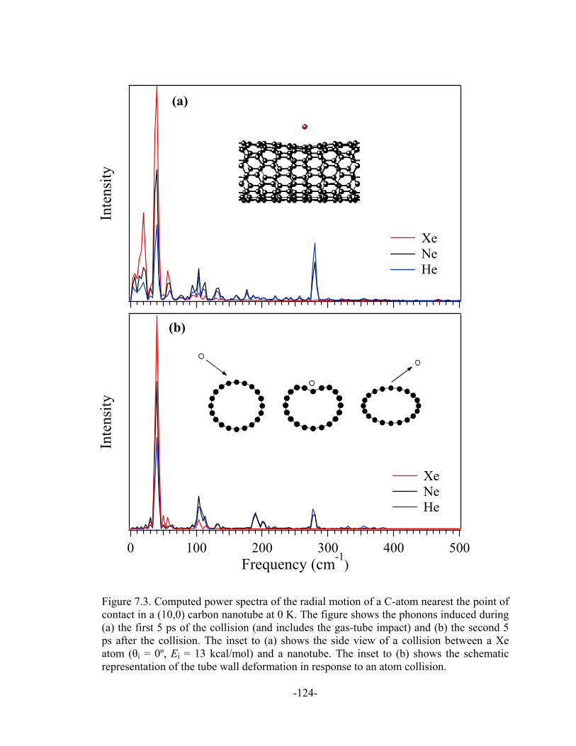
Inte
nsity
Xe Ne He
(a)In
tens
ity
5004003002001000Frequency (cm-1
)
Xe Ne He
(b)
Figure 7.3. Computed power spectra of the radial motion of a C-atom nearest the point of contact in a (10,0) carbon nanotube at 0 K. The figure shows the phonons induced during (a) the first 5 ps of the collision (and includes the gas-tube impact) and (b) the second 5 ps after the collision. The inset to (a) shows the side view of a collision between a Xe atom (θi = 0º, Ei = 13 kcal/mol) and a nanotube. The inset to (b) shows the schematic representation of the tube wall deformation in response to an atom collision.
-124-

Clearly the most prominent peaks in the power spectra increase in strength with the mass
M of the colliding atoms. Furthermore, snapshots of the tube wall motion in time show that the
gas atom impact locally flattens one side of the tube, and then the tube wall near the impact
begins to “ring” or oscillate in an elliptically-shaped deformation identifiable with the Raman-
active “squash” mode (E2g), and the frequency we observe (~ 43 cm-1) is in reasonable agreement
with the calculated squash-mode frequency for a (10,0) nanotube.50 Saito et al.50 have reported
on the strong diameter dependence of the squash mode. Using their calculated squash-mode
frequency for a (10,10) nanotube, we estimate that the squash-mode frequency for a (10,0) tube
is 29 cm-1. The short length of the nanotube, clamped at the ends, may upshift the squash-mode
frequency relative to that obtained for an infinite tube.
Schematics of the tube wall deformation prior to, during, and after collision are shown in
Figure 7.3(b). The side view of a collision is shown in Figure 7.3(a). We find that the energy
dissipation from these squash modes is slow, i.e., the ringing takes place for a long time. These
optical modes have zero group velocity, and for the energy to propagate away from the collision
site, the optical squash mode must first decay into two acoustic modes. In all cases, however, our
simulations show that a significant amount of energy remains near the collision site for 10 ps
after the collision.
Three features from the power spectra in Figure 7.3 are worth mentioning. First, Xe
imparts more energy to the carbon nanotube at the time of impact than does Ne, which, in turn,
imparts more energy than He. However, the strong mass dependence we observe for the
transferred collision energy is lost soon after impact. Second, the low frequency vibrations at ~
43 cm-1 (squash mode) dominate the vibrational power spectrum, and the energy (amplitude) of
this mode is significantly larger after collision with Xe than after collisions with lighter atoms,
-125-
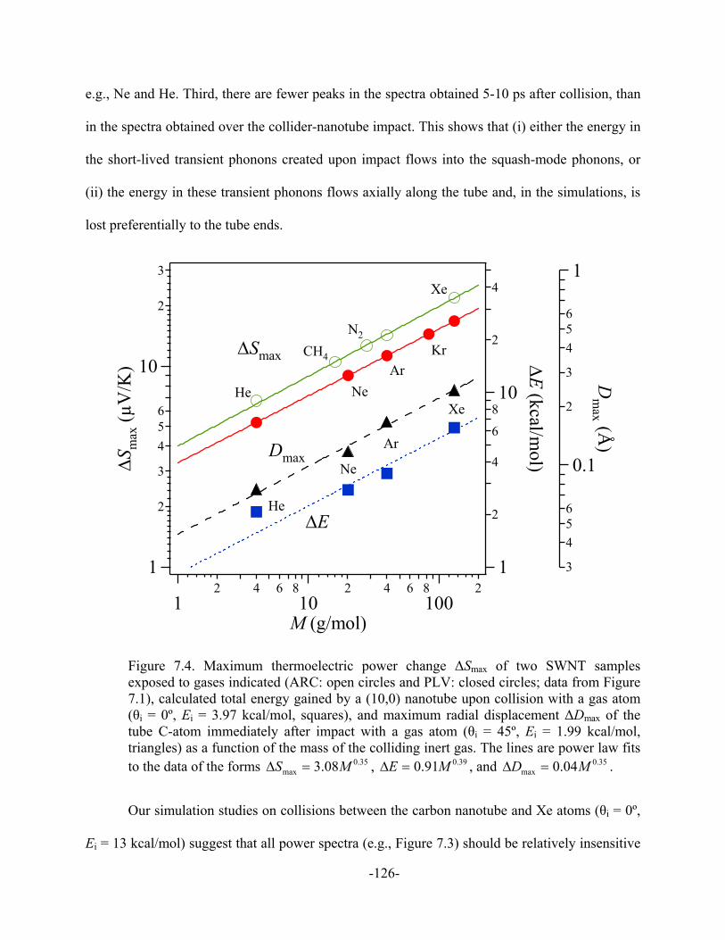
e.g., Ne and He. Third, there are fewer peaks in the spectra obtained 5-10 ps after collision, than
in the spectra obtained over the collider-nanotube impact. This shows that (i) either the energy in
the short-lived transient phonons created upon impact flows into the squash-mode phonons, or
(ii) the energy in these transient phonons flows axially along the tube and, in the simulations, is
lost preferentially to the tube ends.
1
2
3
456
10
2
3
∆Sm
ax (µ
V/K
)
12 4 6 8
102 4 6 8
1002
M (g/mol)
1
2
4
6
810
2
4
∆E (kcal/mol)
3
456
0.1
2
3
456
1
Dm
ax (Å)
He NeAr
Kr
Xe
Ne
He
Xe
CH4
N2
Ar
∆Smax
∆E
Dmax
Figure 7.4. Maximum thermoelectric power change ∆Smax of two SWNT samples exposed to gases indicated (ARC: open circles and PLV: closed circles; data from Figure 7.1), calculated total energy gained by a (10,0) nanotube upon collision with a gas atom (θi = 0º, Ei = 3.97 kcal/mol, squares), and maximum radial displacement ∆Dmax of the tube C-atom immediately after impact with a gas atom (θi = 45º, Ei = 1.99 kcal/mol, triangles) as a function of the mass of the colliding inert gas. The lines are power law fits to the data of the forms , , and . 35.0
max 08.3 MS =∆ 39.091.0 ME =∆ 35.0max 04.0 MD =∆
Our simulation studies on collisions between the carbon nanotube and Xe atoms (θi = 0º,
Ei = 13 kcal/mol) suggest that all power spectra (e.g., Figure 7.3) should be relatively insensitive
-126-
to the incident angle θi of the colliding species. The sole difference we observed is that more
total energy is transferred at smaller incident angles. This is expected, since a smaller incident
angle corresponds to a larger radial component of the gas kinetic energy. Similarly, simulations
of collisions between a Xe atom and a carbon nanotube, where the incident angle was 45º and the
initial energies were 0.40 kcal/mol (200 K), 0.99 kcal/mol (500 K), and 1.99 kcal/mol (1000 K),
showed that the features of the power spectra are insensitive to the initial kinetic energy. The
only difference we observed is that more total energy is transferred to vibrational motion from
higher kinetic energy colliders.
In Figure 7.4, we consider the mass (M) dependence of the colliding atoms or molecules
on ∆Smax (1 atm, 500 K, c.f. Figure 7.1). The straight solid lines in Figure 7.4 represent least-
squares fits to the experimental ∆Smax vs. M (circles) data. Both solid lines exhibit a ~ M1/3
dependence. The closed and the open circles represent the data for the buckypaper and arc-
derived sample, respectively. For comparison, as observed in our molecular dynamics
simulations, we plot the mass dependences of the total energy transfer ∆E (squares) to a short
(10,0) nanotube upon collision (i.e., the total energy lost by the colliding atom), as well as the
maximum radial displacement ∆Dmax (triangles) of the tube C-atom (with which the gas atom
collides) on impact. We find that the slopes of these theoretical lines are insensitive to the
simulation conditions (i.e., incident angle, initial energy, and point of impact). As can be seen in
the figure, the perturbation of the transport properties, the total energy gained by the tube, and
the maximum amplitude of the dent obtained from our simulations all share the same
approximate power law dependence on the collider mass (i.e., M1/3). We also found that the slope
of the theoretical lines of the average tube energy and the maximum radial displacement as a
function of the collider’s mass decreases with time. The polarizability α of inert gases also
-127-

follows a power law dependence with the mass (see Figure 7.5).‡ However, data from small
molecules (N2, CH4) deviate from the power law trend.
0.1
2
4
68
1
2
4
68
10
α (Å
3 )
12 3 4 5 6
102 3 4 5 6
1002
M (g/mol)
α = 0.083×M0.79
HeNe
Ar
Xe
KrN2CH4
Figure 7.5. Dipole polarizability α as a function of the mass of the inert atom or small molecule.
In conclusion, we have observed remarkable experimental effects of collisions of inert
gas atoms (He, Ne, Ar, Kr, and Xe) and small molecules (N2 and CH4) on the thermopower S and
the resistance R of samples of tangled carbon nanotube bundles. At 500 K and 1 atm, the
maximum changes in S and R are proportional to ~ M1/3, where M is the mass of the colliding
species. Our simulations also revealed that the energy exchanged between the tube wall and the
‡ The polarizability of an atom or molecule describes the response of the electron cloud to an external
electric field, E. The induced electric dipole moment is Eα .
-128-

colliding atoms, as well as the maximum deformation of the tube wall as a result of this collision,
exhibits an approximate M1/3 behavior. We propose that the effects we observe in S and R are
due to a new scattering channel for conduction electrons created by collision-induced transient
dents in the tube wall. The pressure saturation of the changes in the transport parameters (R and
S) may be due to the eventual overlap of adjacent dents.
-129-
Chapter 8.
Conclusions and Future Work
Single-walled carbon nanotubes (SWNTs) are now widely accepted as promising
candidates for nanoscale electronic devices on account of their unprecedented electronic
properties. SWNTs provide a unique opportunity to study the interaction of molecules with
conducting surfaces. This stems from the unique structure of the nanotube, i.e., a monolayer
sheet of sp2-bonded carbon (graphene) that is rolled into a small diameter (0.4-2 nm) seamless
cylinder. Since all the carbon atoms reside at the tube surface, the chemical environment in
contact with the nanotube should be expected to influence the transport of electrons in the tube
wall. In addition, although quite strong in tension, the cross-section of a SWNT is easily
deformed, and gas collisions should also be expected to affect the transport of electrons in the
tube wall. This thesis has examined the effects of gas interactions (adsorption and collisions) on
the electrical transport properties (electrical resistance and thermoelectric power) of random
networks of bundled SWNTs.
It has been shown that the measured electronic properties of nanotubes are very sensitive
to their chemical environments. In fact, exposure to air or oxygen (at room temperature)
dramatically influences the electrical resistance and the thermoelectric power of nanotubes.
SWNT samples consisting of randomly oriented bundles of hundreds of nanotubes exhibit a
gradual crossover of thermopower from a large positive value to a large negative value, as
adsorbed oxygen is removed from the sample in high vacuum at elevated temperatures (~ 500 K),
in agreement with previous results.89,90 In addition, we have observed that the thermoelectric
power can be reliably and reversibly “tuned” simply by controlling the amount of oxygen
-130-

adsorbed on the tube walls at low temperatures. Interestingly, independent of the amount of
oxygen adsorbed, the thermoelectric power retains the typical behavior of purified, macroscopic
samples: a dominant quasi-linear component with a superimposed knee or smooth change of
slope at ~ 100 K. The quasi-linear behavior suggests that metallic tubes in the sample dominate
the thermoelectric power. To explain these results, a weak charge transfer between the O2
molecules and the SWNTs to form a complex where δ ≤ 0.1, has been proposed.
Model calculations of the thermoelectric power has been presented which show that, in the
general case, the thermoelectric power is determined by coordinated effects in both the
semiconducting and the metallic nanotubes in the SWNT rope. That is, the sign and magnitude
of the thermoelectric power can be determined by the near mirror symmetry bands in metallic
nanotubes and density of states resonances near the Fermi energy which, in turn, are determined
by the balance between acceptor (charged species that can be removed by vacuum-
degassing) and donor states on the semiconducting nanotubes, possibly due to wall defects.
δδ+ − -2p OC
δ-2O
Before one can hope to fully rationalize the aforementioned effects of exposure to
molecular oxygen on the electronic transport properties of SWNTs, the phenomenon of O2
adsorption needs to be better understood. Specifically, the issue of whether O2 molecules are
physisorbed or chemisorbed on the SWNT walls needs to be resolved. In addition to resolving
this controversy, one should be able to model the effects of O2 adsorption on the electrical
conductance of SWNTs and to include potential effects of the contacts between SWNTs and
leads attached to their ends during experimental measurements. The importance of the sensitivity
of carbon nanotubes to O2 need not be over-emphasized, as it raises questions about the stability
of carbon nanotube devices to air exposure. On the other hand, the observed effects of O2
exposure on the carbon nanotubes properties raises the possibility that unintentional oxygen
-131-

contamination during sample preparation may lead to incorrect analysis of the experimental data.
It has been suggested that O2 in proximity to a wall defect may lead to the formation of the
charge transfer complex. Further work is needed to prove this hypothesis.
The second contribution to the “intrinsic” thermoelectric power we have observed is in
the form of a knee or a broad peak at ~ 100 K (superimposed on a linear, metallic background).
We propose that this peak should not be identified with a Kondo anomaly, as proposed
previously,76 but rather should be attributed to the phonon drag effect. To calculate the phonon
drag contribution, a variational solution to the coupled electron-phonon Boltzmann equations
was used.119 The calculation also involved the use of a simple tight-binding model for the
electronic structure of metallic armchair tubes, a linear acoustic phonon dispersion, and a
temperature-independent phonon relaxation time. The relevant phonon wave vectors contributing
to the phonon drag effect are determined by the Fermi level position which, in turn, is
determined by the oxygen content in the SWNTs. This model describes very well the unusual
behavior of the experimental thermopower in purified and as-grown SWNT materials, as long as
the broad peak is not so pronounced, as in the case of SWNT material grown and containing Co-
Y and Fe-Y catalysts. For these Co-Y and Fe-Y samples, quantitative agreement with our simple
theory is lacking, but the discrepancy may be reconciled if an appropriate temperature-
dependence of the phonon lifetime is incorporated into the model.
The transport properties of SWNTs have also been shown to be most sensitive to gases
that chemisorb and undergo weak charge transfer reactions (e.g., O2 and NH3) with the
nanotubes. Surprisingly, the transport parameters (thermoelectric power and electrical resistance)
haver even been found to be sensitive to physisorption of gases and chemical vapors (e.g., H2,
alcohols, and cyclic hydrocarbons) and gas collisions with the carbon nanotube walls (e.g., inert
-132-
gases, N2, CH4). For polar molecules (alcohols and water), the trends in the measured
perturbations of the transport properties could be explained on the basis of the interplay between
the adsorption energy and the molecular coverage on the nanotube surfaces. Interestingly, the
thermoelectric power response to water vapor was found to be very weak, although the resistive
response to water vapor exposure was similar to that to simple alcohols exposure. For six-
membered-ring molecules, the magnitudes of the changes in the transport properties were found
to be related to the π electron population of the molecule, suggesting that the coupling between
these π electrons in the adsorbed molecules and those in the nanotube wall may be responsible
for the observed effects. In our studies on gas collisions (He, Ne, Ar, Kr, Xe, N2, CH4) on the
SWNT surface, the unusually strong and systematic changes in the transport properties have
been found to scale as ~ M1/3 (M is the mass of the colliding gas atom or molecule)–the same
dependence exhibited by the total energy transfer to the nanotube and the maximum deformation
of the tube upon collision. Molecular simulations by Kim Bolton and Arne Rosén (Göteborg
University and Chalmers University of Technology) have supported the idea that a significant
transient population of low-frequency phonons (squash-mode phonons) is created upon collisions,
which could then provide the new scattering mechanism for the conduction electrons in the tube
walls. This could be direct atom-electron scattering, but the observed M1/3 dependence of the
wall deformation is compelling evidence for deformation scattering.
The mechanism we have proposed to explain the thermoelectric changes in SWNTs upon
interaction with gases and chemicals is the creation of an additional scattering channel for
conduction electrons in the nanotube wall created by physisorption or gas collisions with the tube
wall. The expression developed for this model follows from the Mott relation for the
thermoelectric power of metals and the Matheissen’s rule, which is equivalent to the additive
-133-

nature of independent scattering mechanisms. The same expression was developed previously to
discuss the thermoelectric behavior of Au and Ag alloys, and is known as the Nordheim-Gorter
relation. We believe that the sensitivity of Nordheim-Gorter plots at a fixed temperature to
different molecules can be the basis for the utility of a SWNT thermoelectric “nano-nose”. In
fact, the sensitivities of S and R to coverage must be related to the quasi-one-dimensional nature
of the transport in SWNTs, and to the fact that almost all carbon atoms are associated with one
adsorption site or another. Detailed theoretical calculations to investigate the scattering
mechanisms for various adsorption sites and molecules are now needed. These calculations
would allow understanding why, unlike other gases (e.g., N2, He, etc.), exposure of the
nanotubes to H2 give rise to negative slopes in the S vs. ∆R/R0 plots. It would be interesting to
study the effects of H2, D2, and HD exposures on the same SWNT sample to determine the
relative contributions from collisions and chemical interactions to the electrical transport
properties.
The purity of SWNT samples is limited by the extensive use of metal catalysts in the
growth process and chemicals during purification and dispersion procedures. Unfortunately, in
spite of accurate protocols for elimination of chemicals, traces may still remain in the sample as
undesired and often unrevealed contaminants, which might interference with SWNT interactions
with adsorbates.109 This indicates the extreme importance of careful determination of the
chemical purity of samples subjected to purification processes and thus unintentionally
contaminated, as the presence of extrinsic contaminant species on the tube walls can mimic
electronic properties different from the intrinsic electronic properties of nanotubes. It is thus
important to investigate the thermoelectric power of functionalized nanotubes. Moreover, the
structure of SWNTs is increasingly altered by the introduction of defects due to the effect of
-134-

chemical treatments with increasing strength.199 Although, structural defects and side openings
can be cured to some extent by subsequent annealing, the effects of different types of defects on
the electronic properties of carbon nanotubes in the presence of gases and chemicals need to be
further investigated.
There are significant disadvantages to our measurements on “bulk” samples for
understanding the intrinsic properties of a single nanotube. One problem is that these
measurements yield an ensemble average over the different tubes in a sample. More importantly,
the numerous tube-tube junctions present in these macroscopic samples make it difficult to
extract absolute values from the transport properties. Mesoscopic scale measurements able to
probe individual nanotubes are necessary in order to elucidate their intrinsic transport properties.
In conclusion, the work presented here emphasizes the effects of gaseous molecules on
the electrical transport of carbon nanotubes. The knowledge acquired may have important
implications on the production and growth, as well as the applications of carbon nanotubes.
Theoretical calculations to investigate the scattering mechanisms for various adsorption sites and
molecules are now needed. As these calculations will have to deal with the details of the
molecule-SWNT interactions, it is hoped that these calculations and the data presented here will
provide quantitative insight into the details of gas-SWNT interactions.
-135-

Appendix A:
Derivation of the Mott Relation
An alternative and general expression for the thermoelectric power S is to write:
( ) , )(1F ε
εεσ−ε
σ= ∫ d
ddfE
eTS (A.1)
where
. )()()(
, )(
εµε≡εσ
εε
εσ−=σ ∫eN
dddf
(A.2)
Here σ is the electrical conductivity, N(ε) is the density of states, µ(ε) is the mobility at a given
energy level ε, and f(ε) is the equilibrium electron distribution function. If the scattering is weak
and the mean free path is long, Eqs. (A.1) and (3.2) give essentially identical results.
Let us consider a general equation of the form,
. )(0∫∞
εε
ε−= dddfhI (A.3)
When only states near EF contribute to the current, εddf will be appreciable only within
a few kBT of EF. In this case, it is very reasonable to evaluate Eq. (A.3) by expanding the
integrand about EF which leads to a rapidly converging series:
, 1
1!0 0
∫ ∑∞
−
∞
= =⎟⎟⎠
⎞⎜⎜⎝
⎛+⎥
⎥⎦
⎤
⎢⎢⎣
⎡⎟⎟⎠
⎞⎜⎜⎝
⎛−=
TkE
yn y
n
nn
BF
dyedy
ddy
hdnyI (A.4)
where ( ) TkEy BF−ε= . Since the expansion converges rapidly only if 1F >>TkE B , the lower
-136-

limit of the integral on this integral can be replaced by −∞. The result is
( )
( ) , )2(2
12
, )(
12
12
22
F
F
nC
dhdTkCEhI
nn
n En
nn
Bn
ζ⎟⎠⎞
⎜⎝⎛ −=
⎟⎟⎠
⎞⎜⎜⎝
⎛ε
+=
−
∞
= =ε
∑ (A.5)
where ξ(n) is the Riemann zeta function.
Keeping only the first terms in the summation,
( ) . 6
)(F
2
22
2
FE
B dhdTkEhI
=ε⎟⎟⎠
⎞⎜⎜⎝
⎛ε
π+=
Let ( )[ ]TkEh BF)()( −εεσ=ε , hence
( ) . )(2)()(2)(
FFF
2
2F
2
2
EBEBBE dd
Tkdd
TkE
dd
Tkdhd
=ε=ε=ε
⎟⎠⎞
⎜⎝⎛
εεσ
=⎥⎦
⎤⎢⎣
⎡ε
εσ−ε+
εεσ
=ε
ε
Substituting this result into Eq. (A.1),
( ) ( )
, )(13
)(26
1
F
F
2
22
F
E
B
EBB
dd
eTk
dd
TkTk
EeS
=ε
=ε
⎟⎠⎞
⎜⎝⎛
εεσ
σπ
=
⎥⎥⎦
⎤
⎢⎢⎣
⎡⎟⎠⎞
⎜⎝⎛
εεσπ
σ=
or
. ln3
F
22
E
B
dd
eTkS
=ε
⎟⎠⎞
⎜⎝⎛
εσπ
= (A.6)
This is the familiar Mott formula for metallic conduction.
Although Eq. (A.6) has been derived here with the aid of the relaxation time
approximation, the result is generally valid provided the conduction electrons constitute a
degenerate Fermi gas, so that higher-order terms in the expansion (A.5) are negligible.
-137-

Appendix B:
Derivation of the Phonon Drag Thermopower
Simple derivations of the expression for phonon drag thermopower are usually based on
the ideas of “balance forces” and “momentum transfer” between the phonon and electron
systems. Here, we provide an alternative picture based on “current balance” model for the
Seebeck effect, i.e.
, 0total =++= ges JJJJ (B.1)
where Je is the electric current density arising from the maintained temperature gradient
produced by the electron diffusion mechanism, Jg is produced by the phonon drag mechanism
and Js is the current density produced in the steady state to counteract Je + Jg, driven by the
Seebeck voltage.
The Seebeck current can be written as:
, 'EJs σ= (B.2)
where σ is the electrical conductivity and ( ) µ∇−= eEE 1' ; E is the electric field, and µ is the
chemical potential. Hence,
. '
0=
⎟⎠⎞
⎜⎝⎛
∇=
JTES (B.3)
The current Jg is defined in the form
( ) [ , 2
'',''
coll ∑∑ −⎟
⎠⎞
⎜⎝⎛
∂∂
−Ω
=− jj
jjep
g llet
NJkk
kkq
q ] (B.4)
-138-

where is the phonon distribution function, is the mean free path of an electron with
wave vector k in the band j, and Ω is the volume. The term
( )qN jlk
( )coll ep
tN−
∂∂− q is the number of
phonons leaving state q per unit time due to the phonon-electron collision mechanism; [ ]'' jj ll kk −
is the average change in electron mean free path in the direction of the temperature gradient
arising from absorption of a phonon in state q.
We now make the following assumptions:
(1) ( ) ( ) ( ) ; '',;coll allcoll t
Njjt
N
p-e ∂∂
α=∂
∂ qkkqq (B.5)
in other words we introduce the factor ( )'',; jj kkqα which is equal to the fraction of phonon-
electron collisions to all phonon collisions.
(2) A Boltzmann equation for the phonon distribution ( )qN can be used:
( ) ( ) . 0driftcoll all
=∂
∂+
∂∂
tN
tN qq (B.6)
(3) An electron relaxation time treatment is valid:
(B.7) . jjj vl kkk τ=
The conventional treatment of ( )drift
tN ∂∂ q is:
( ) ( ) . 0
drift
TVT
Nt
N∇
∂∂
−=∂
∂q
qq (B.8)
Hence using the three assumptions listed above, Eq. (B.4) becomes
( ) ( ) [ . '',;2
'',''''
0 ∑∑ τ−τα∇∂
∂Ω
−=jj
jjjjg vvVjjTT
NeJ
kkkkκkq
q
kkqq ] (B.9)
Returning to the current balance picture [Eq. (B.1)] and neglecting Je, we finally obtain
-139-

( ) ( ) [ ], '',;2
''
'',''''
0
0
∑∑ τ−τα∂
∂Ωσ
=
∇−=⎟
⎠⎞
⎜⎝⎛
∇=
=
jjjjjj
B
e
g
Jg
vvVjjT
NkeEJTJ
TES
kkkkkkq
q
kkqq (B.10)
and assuming an isotropic material,
( ) ( )[ , '',;2
'',''''
0q
kkkkkk
q
Vvvkkqq⋅τ−τα
∂∂
σΩ= ∑∑
jjjjjjg jj
TN
de
S ] (B.11)
where d is the dimensionality of the system.
-140-

Bibliography
[1] S. Iijima, "Helical microtubules of graphitic carbon." Nature 354, 56 (1991).
[2] M. Endo, "The growth mechanism of vapor-grown carbon fibers." Ph.D. thesis,
University of Orleans, Orleans, France (1975).
[3] M. S. Dresselhaus, G. Dresselhaus, and P. C. Eklund, Science of fullerenes and carbon
nanotubes. (Academic Press, San Diego, 1996).
[4] S. Frank, P. Poncharal, Z. L. Wang, and W. A. de Heer, "Carbon nanotube quantum
resistors." Science 280, 1744 (1998).
[5] W. Liang, M. Bockrath, D. Bozovic, J. H. Hafner, M. Tinkham, and H. Park, "Fabry-
Perot interference in a nanotube electron waveguide." Nature 411, 665 (2001).
[6] P. Poncharal, C. Berger, Y. Yi, Z. L. Wang, and W. A. de Heer, "Room temperature
ballistic conduction in carbon nanotubes." Journal of Physical Chemistry B 106 (47),
12104 (2002).
[7] D. Mann, A. Javey, J. Kong, Q. Wang, and H. Dai, "Ballistic transport in metallic
nanotubes with reliable Pd ohmic contacts." Nano Letters, ACS ASAP.
[8] P. Kim, L. Shi, A. Majumdar, and P. L. McEuen, "Thermal transport measurements of
individual multiwalled nanotubes." Physical Review Letters 87 (21), 215502 (2001).
[9] E. W. Wong, P. E. Sheehan, and C. M. Lieber, "Nanobeam mechanics: elasticity, strength,
and toughness of nanorods and nanotubes." Science 277, 1971 (1997).
[10] B. I. Yakobson and P. Avouris, "Mechanical properties of carbon nanotubes." Topics in
Applied Physics 80 (Carbon Nanotubes), 287 (2001).
[11] M. S. Dresselhaus, "Future directions in carbon science." Annual Review of Materials
Science 27, 1 (1997).
-141-

[12] R. H. Baughman, A. A. Zakhidov, and W. A. de Heer, "Carbon nanotubes-the route
toward applications." Science 297, 787 (2002).
[13] P. M. Ajayan and O. Z. Zhou, "Applications of carbon nanotubes." Topics in Applied
Physics 80 (Carbon Nanotubes), 391 (2001).
[14] D. Qian, E. C. Dickey, R. Andrews, and T. Rantell, "Load transfer and deformation
mechanisms in carbon nanotube-polystyrene composites." Applied Physics Letters 76
(20), 2868 (2000).
[15] M. J. Biercuk, M. C. Llaguno, M. Radosavljevic, J. K. Hyun, A. T. Johnson, and J. E.
Fischer, "Carbon nanotube composites for thermal management." Applied Physics
Letters 80 (15), 2767 (2002).
[16] C. Niu, E. K. Sichel, R. Hoch, D. Moy, and H. Tennent, "High power electrochemical
capacitors based on carbon nanotube electrodes." Applied Physics Letters 70 (11), 1480
(1997).
[17] R. H. Baughman, C. Cui, A. A. Zakhidov, Z. Iqbal, J. N. Barisci, G. M. Spinks, G. G.
Wallace, A. Mazzoldi, D. De Rossi, A. G. Rinzler, O. Jaschinski, S. Roth, and M. Kertesz,
"Carbon nanotube actuators." Science 284, 1340 (1999).
[18] J. Kong, N. R. Franklin, C. Zhou, M. G. Chapline, S. Peng, K. Cho, and H. Dai,
"Nanotube molecular wires as chemical sensors." Science 287, 622 (2000).
[19] A. Modi, N. Koratkar, E. Lass, B. Wei, and P. M. Ajayan, "Miniaturized gas ionization
sensors using carbon nanotubes." Nature 424, 171 (2003).
[20] W. A. de Heer, A. Chatelain, and D. Ugarte, "A carbon nanotube field-emission electron
source." Science 270, 1179 (1995).
[21] A. G. Rinzler, J. H. Hafner, P. Nikolaev, L. Lou, S. G. Kim, D. Tomanek, P. Nordlander,
D. T. Colbert, and R. E. Smalley, "Unraveling nanotubes: field emission from an atomic
wire." Science 269, 1550 (1995).
-142-

[22] Q. H. Wang, A. A. Setlur, J. M. Lauerhaas, J. Y. Dai, E. W. Seelig, and R. P. H. Chang,
"A nanotube-based field-emission flat panel display." Applied Physics Letters 72 (22),
2912 (1998).
[23] Y. Saito, S. Uemura, and K. Hamaguchi, "Cathode ray tube lighting elements with carbon
nanotube field emitters." Japanese Journal of Applied Physics, Part 2: Letters 37 (3B),
L346 (1998).
[24] R. Rosen, W. Simendinger, C. Debbault, H. Shimoda, L. Fleming, B. Stoner, and O.
Zhou, "Application of carbon nanotubes as electrodes in gas discharge tubes." Applied
Physics Letters 76 (13), 1668 (2000).
[25] N. S. Lee, D. S. Chung, I. T. Han, J. H. Kang, Y. S. Choi, H. Y. Kim, S. H. Park, Y. W.
Jin, W. K. Yi, M. J. Yun, J. E. Jung, C. J. Lee, J. H. You, S. H. Jo, C. G. Lee, and J. M.
Kim, "Application of carbon nanotubes to field emission displays." Diamond and Related
Materials 10 (2), 265 (2001).
[26] A. C. Dillon, K. M. Jones, T. A. Bekkedahl, C. H. Kiang, D. S. Bethune, and M. J. Heben,
"Storage of hydrogen in single-walled carbon nanotubes." Nature 386, 377 (1997).
[27] P. Chen, X. Wu, J. Lin, and K. L. Tan, "High H2 uptake by alkali-doped carbon
nanotubes under ambient pressure and moderate temperatures." Science 285, 91 (1999).
[28] C. Liu, Y. Y. Fan, M. Liu, H. T. Cong, H. M. Cheng, and M. S. Dresselhaus, "Hydrogen
storage in single-walled carbon nanotubes at room temperature." Science 286, 1127
(1999).
[29] Y. Ye, C. C. Ahn, C. Witham, B. Fultz, J. Liu, A. G. Rinzler, D. Colbert, K. A. Smith,
and R. E. Smalley, "Hydrogen adsorption and cohesive energy of single-walled carbon
nanotubes." Applied Physics Letters 74 (16), 2307 (1999).
[30] Y. Chen, D. T. Shaw, X. D. Bai, E. G. Wang, C. Lund, W. M. Lu, and D. D. L. Chung,
"Hydrogen storage in aligned carbon nanotubes." Applied Physics Letters 78 (15), 2128
(2001).
-143-

[31] G. G. Tibbetts, G. P. Meisner, and C. H. Olk, "Hydrogen storage capacity of carbon
nanotubes, filaments, and vapor-grown fibers." Carbon 39 (15), 2291 (2001).
[32] J. H. Hafner, C. Li Cheung, and C. M. Lieber, "Growth of nanotubes for probe
microscopy tips." Nature 398, 761 (1999).
[33] S. S. Wong, E. Joselevich, A. T. Woolley, C. Li Cheung, and C. M. Lieber, "Covalently
functionalized nanotubes as nanometer-sized probes in chemistry and biology." Nature
394, 52 (1998).
[34] P. Kim and C. M. Lieber, "Nanotube nanotweezers." Science 286, 2148 (1999).
[35] M. S. Fuhrer, J. Nygard, L. Shih, M. Forero, Y.-G. Yoon, M. S. C. Mazzoni, H. J. Choi, J.
Ihm, S. G. Louie, A. Zettl, and P. L. McEuen, "Crossed nanotube junctions." Science 288,
494 (2000).
[36] T. Rueckes, K. Kim, E. Joselevich, G. Y. Tseng, C.-L. Cheung, and C. M. Lieber,
"Carbon nanotube-based nonvolatile random access memory for molecular computing."
Science 289, 94 (2000).
[37] S. J. Tans, A. R. M. Verschueren, and C. Dekker, "Room-temperature transistor based on
a single carbon nanotube." Nature 393, 49 (1998).
[38] R. Martel, T. Schmidt, H. R. Shea, T. Hertel, and P. Avouris, "Single- and multi-wall
carbon nanotube field-effect transistors." Applied Physics Letters 73 (17), 2447 (1998).
[39] A. Bachtold, P. Hadley, T. Nakanishi, and C. Dekker, "Logic circuits with carbon
nanotube transistors." Science 294, 1317 (2001).
[40] S. Iijima and T. Ichihashi, "Single-shell carbon nanotubes of 1-nm diameter." Nature 363,
603 (1993).
[41] D. S. Bethune, C. H. Kiang, M. S. de Vries, G. Gorman, R. Savoy, J. Vazquez, and R.
Beyers, "Cobalt-catalyzed growth of carbon nanotubes with single-atomic-layer walls."
Nature 363, 605 (1993).
-144-

[42] A. Thess, R. Lee, P. Nikolaev, H. Dai, P. Petit, J. Robert, C. Xu, Y. H. Lee, S. G. Kim, D.
T. Colbert, G. Scuseria, D. Tománek, J. E. Fischer, and R. E. Smalley, "Crystalline ropes
of metallic carbon nanotubes." Science 273, 483 (1996).
[43] C. Journet, W. K. Maser, P. Bernier, A. Loiseau, M. Lamy de la Chapells, S. Lefrant, P.
Deniard, R. Lee, and J. E. Fischer, "Large-scale production of single-walled carbon
nanotubes by the electric-arc technique." Nature 388, 756 (1997).
[44] C. Dekker, "Carbon nanotubes as molecular quantum wires." Physics Today 52 (5), 22
(1999).
[45] J. Nygard, D. H. Cobden, M. Bockrath, P. L. McEuen, and P. E. Lindelof, "Electrical
transport measurements on single-walled carbon nanotubes." Applied Physics A 69 (3),
297 (1999).
[46] Z. Yao, C. Dekker, and P. Avouris, "Electrical transport through single-wall carbon
nanotubes." Topics in Applied Physics 80 (Carbon Nanotubes), 147 (2001).
[47] L.-C. Qin, X. Zhao, K. Hirahara, Y. Miyamoto, Y. Andos, and S. Iijima, "Materials
science: The smallest carbon nanotube." Nature 408, 50 (2000).
[48] N. Wang, Z. K. Tang, G. D. Li, and J. S. Chen, "Materials science: Single-walled 4 Å
carbon nanotube arrays." Nature 408, 50 (2000).
[49] B. Wei, R. Vajtai, Y. Y. Choi, P. M. Ajayan, H. Zhu, C. Xu, and D. Wu, "Structural
characterizations of long single-walled carbon nanotube strands." Nano Letters 2 (10),
1105 (2002).
[50] R. Saito, G. Dresselhaus, and M. S. Dresselhaus, Physical properties of carbon
nanotubes. (Imperial College Press, London, 1998).
[51] T. W. Odom, J.-L. Huang, P. Kim, and C. M. Lieber, "Atomic structure and electronic
properties of single-walled carbon nanotubes." Nature 391, 62 (1998).
[52] P. R. Wallace, "The band theory of graphite." Physical Review 71, 622 (1947).
-145-

[53] M. S. Dresselhaus and P. C. Eklund, "Phonons in carbon nanotubes." Advances in
Physics 49 (6), 705 (2000).
[54] A. M. Rao, E. Richter, S. Bandow, B. Chase, P. C. Eklund, K. A. Williams, S. Fang, K. R.
Subbaswamy, M. Menon, A. Thess, R. E. Smalley, G. Dresselhaus, and M. S.
Dresselhaus, "Diameter-selective Raman scattering from vibrational modes in carbon
nanotubes." Science 275, 187 (1997).
[55] M. S. Dresselhaus, G. Dresselhaus, P. Eklund, and R. Saito, "Carbon nanotubes." Physics
World 11 (1), 33 (1998).
[56] K. A. Williams and P. C. Eklund, "Monte Carlo simulations of H2 physisorption in finite-
diameter carbon nanotube ropes." Chemical Physics Letters 320 (3/4), 352 (2000).
[57] A. C. Dillon and M. J. Heben, "Hydrogen storage using carbon adsorbents: past, present
and future." Applied Physics A 72 (2), 133 (2001).
[58] H. Dai, "Carbon nanotubes: opportunities and challenges." Surface Science 500 (1-3),
218 (2002).
[59] C. W. Zhou, J. Kong, E. Yenilmez, and H. J. Dai, "Modulated chemical doping of
individual carbon nanotubes." Science 290, 1552 (2000).
[60] P. C. Eklund, J. M. Holden, and R. A. Jishi, "Vibrational modes of carbon nanotubes;
spectroscopy and theory." Carbon 33 (7), 959 (1995).
[61] S. Bandow, S. Asaka, Y. Saito, A. M. Rao, L. Grigorian, E. Richter, and P. C. Eklund,
"Effect of the growth temperature on the diameter distribution and chirality of single-wall
carbon nanotubes." Physical Review Letters 80 (17), 3779 (1998).
[62] U. D. Venkateswaran, A. M. Rao, E. Richter, M. Menon, A. Rinzler, R. E. Smalley, and
P. C. Eklund, "Probing the single-wall carbon nanotube bundle: Raman scattering under
high pressure." Physical Review B 59 (16), 10928 (1999).
[63] L. Henrard, E. Hernandez, P. Bernier, and A. Rubio, "Van der Waals interaction in
-146-

nanotube bundles. Consequences on vibrational modes." Physical Review B 60 (12),
R8521 (1999).
[64] D. Kahn and J. P. Lu, "Vibrational modes of carbon nanotubes and nanoropes." Physical
Review B 60 (9), 6535 (1999).
[65] L. Alvarez, A. Righi, T. Guillard, S. Rols, E. Anglaret, D. Laplaze, and J. L. Sauvajol,
"Resonant Raman study of the structure and electronic properties of single-wall carbon
nanotubes." Chemical Physics Letters 316 (3/4), 186 (2000).
[66] A. G. Rinzler, J. Liu, H. Dai, P. Nikolaev, C. B. Huffman, F. J. Rodriguez-Macias, P. J.
Boul, A. H. Lu, D. Heymann, D. T. Colbert, R. S. Lee, J. E. Fischer, A. M. Rao, P. C.
Eklund, and R. E. Smalley, "Large-scale purification of single-wall carbon nanotubes:
Process, product, and characterization." Applied Physics A 67 (1), 29 (1998).
[67] P. C. Eklund and A. K. Mabatah, "Thermoelectric power measurements using analog
subtraction." Review of Scientific Instruments 48 (7), 775 (1977).
[68] G. U. Sumanasekera, L. Grigorian, and P. C. Eklund, "Low-temperature thermoelectrical
power measurements using analogue subtraction." Measurement Science & Technology
11 (3), 273 (2000).
[69] D. K. C. MacDonald, Thermoelectricity: an introduction to the principles. (Wiley, New
York, 1962).
[70] R. D. Barnard, Thermoelectricity in metals and alloys. (Taylor & Francis, London, 1972).
[71] F. J. Blatt, P. A. Schroeder, C. L. Foiles, and D. Greig, Thermoelectric power of metals.
(Plenum Press, New York, 1976).
[72] H. Fritzsche, "General expression for the thermoelectric power." Solid State
Communications 9 (21), 1813 (1971).
[73] F. J. Blatt, Physics of electronic conduction in solids. (McGraw-Hill, New York, 1968).
[74] J. Hone, I. Ellwood, M. Muno, A. Mizel, M. L. Cohen, A. Zettl, A. G. Rinzler, and R. E.
-147-

Smalley, "Thermoelectric power of single-walled carbon nanotubes." Physical Review
Letters 80 (5), 1042 (1998).
[75] L. Grigorian, K. A. Williams, S. Fang, G. U. Sumanasekera, A. L. Loper, E. C. Dickey, S.
J. Pennycook, and P. C. Eklund, "Reversible intercalation of charged iodine chains into
carbon nanotube ropes." Physical Review Letters 80 (25), 5560 (1998).
[76] L. Grigorian, G. U. Sumanasekera, A. L. Loper, S. L. Fang, J. L. Allen, and P. C. Eklund,
"Giant thermopower in carbon nanotubes: A one-dimensional Kondo system." Physical
Review B 60 (16), R11309 (1999).
[77] B. T. Kelly, Physics of graphite. (Applied Science Publishers, London, 1981).
[78] A. B. Kaiser, Y. W. Park, G. T. Kim, E. S. Choi, G. Dusberg, and S. Roth, "Electronic
transport in carbon nanotube ropes and mats." Synthetic Metals 103 (1-3), 2547 (1999).
[79] G. C. McIntosh and A. B. Kaiser, "Calculating thermopower due to fluctuation-assisted
tunneling with application to carbon nanotube ropes." Current Applied Physics 1, 145
(2001).
[80] M. Baxendale, K. G. Lim, and G. A. J. Amaratunga, "Thermoelectric power of aligned
and randomly oriented carbon nanotubes." Physical Review B 61 (19), 12705 (2000).
[81] J. W. G. Wildoer, L. C. Venema, A. G. Rinzier, R. E. Smalley, and C. Dekker,
"Electronic structure of atomically resolved carbon nanotubes." Nature 391, 59 (1998).
[82] P. L. McEuen, M. Bockrath, D. H. Cobden, Y.-G. Yoon, and S. G. Louie, "Disorder,
pseudospins, and backscattering in carbon nanotubes." Physical Review Letters 83 (24),
5098 (1999).
[83] P. G. Collins, M. S. Arnold, and P. Avouris, "Engineering carbon nanotubes and
nanotube circuits using electrical breakdown." Science 292, 706 (2001).
[84] Y. Zvyagin, in Hopping transport in solids, edited by B. I. Shklovskii (North Holland,
New York, 1991).
-148-

[85] E. S. Choi, D. S. Suh, G. T. Kim, D. C. Kim, and Y. W. Park, "Magnetothermopower of
single wall carbon nanotube newtwork." Synthetic Metals 103 (1-3), 2504 (1999).
[86] P. Sheng, "Fluctuation-induced tunneling conduction in disordered materials." Physical
Review B 21 (6), 2180 (1980).
[87] G. D. Mahan, Many-particle physics, 3rd ed. (Kluwer Academic/Plenum Publishers, New
York, 2000).
[88] K. Bradley, S. -H. Jhi, P. G. Collins, J. Hone, M. L. Cohen, S. G. Louie, and A. Zettl, "Is
the intrinsic thermoelectric power of carbon nanotubes positive?" Physical Review
Letters 85 (20), 4361 (2000).
[89] G. U. Sumanasekera, C. K. W. Adu, S. Fang, and P. C. Eklund, "Effects of gas
adsorption and collisions on electrical transport in single-walled carbon nanotubes."
Physical Review Letters 85 (5), 1096 (2000).
[90] P. G. Collins, K. Bradley, M. Ishigami, and A. Zettl, "Extreme oxygen sensitivity of
electronic properties of carbon nanotubes." Science 287, 1801 (2000).
[91] S. Peng and K. Cho, "Chemical control of nanotube electronics." Nanotechnology 11 (2),
57 (2000).
[92] S.-H. Jhi, S. G. Louie, and M. L. Cohen, "Electronic properties of oxidized carbon
nanotubes." Physical Review Letters 85 (8), 1710 (2000).
[93] X. Y. Zhu, S. M. Lee, Y. H. Lee, and T. Frauenheim, "Adsorption and desorption of an
O2 molecule on carbon nanotubes." Physical Review Letters 85 (13), 2757 (2000).
[94] D. C. Sorescu, K. D. Jordan, and P. Avouris, "Theoretical study of oxygen adsorption on
graphite and the (8,0) single-walled carbon nanotube." Journal of Physical Chemistry B
105 (45), 11227 (2001).
[95] J. Zhao, A. Buldum, J. Han, and J. P. Lu, "Gas molecule adsorption in carbon nanotubes
and nanotube bundles." Nanotechnology 13 (2), 195 (2002).
-149-

[96] A. Ricca and J. A. Drocco, "Interaction of O2 with a (9,0) carbon nanotube." Chemical
Physics Letters 362 (3,4), 217 (2002).
[97] S.-P. Chan, G. Chen, X. G. Gong, and Z.-F. Liu, "Oxidation of carbon nanotubes by
singlet O2." Physical Review Letters 90 (8), 086403 (2003).
[98] S. Dag, O. Gulseren, T. Yildirim, and S. Ciraci, "Oxygenation of carbon nanotubes:
atomic structure, energetics, and electronic structure." Physical Review B 67 (16),
165424 (2003).
[99] G. E. Froudakis, M. Schnell, M. Muhlhauser, S. D. Peyerimhoff, A. N. Andriotis, M.
Menon, and R. M. Sheetz, "Pathways for oxygen adsorption on single-wall carbon
nanotubes." Physical Review B 68 (11), 115435 (2003).
[100] M. Grujicic, G. Cao, A. M. Rao, T. M. Tritt, and S. Nayak, "UV-light enhanced oxidation
of carbon nanotubes." Applied Surface Science 214 (1-4), 289 (2003).
[101] M. Grujicic, G. Cao, and R. Singh, "The effect of topological defects and oxygen
adsorption on the electronic transport properties of single-walled carbon-nanotubes."
Applied Surface Science 211 (1-4), 166 (2003).
[102] P. Giannozzi, R. Car, and G. Scoles, "Oxygen adsorption on graphite and nanotubes."
Journal of Chemical Physics 118 (3), 1003 (2003).
[103] A. Ricca, C. W. Bauschlicher, Jr., and A. Maiti, "Comparison of the reactivity of O2 with
a (10,0) and a (9,0) carbon nanotube." Physical Review B 68 (3), 035433 (2003).
[104] V. Derycke, R. Martel, J. Appenzeller, and P. Avouris, "Carbon nanotube inter- and
intramolecular logic gates." Nano Letters 1 (9), 453 (2001).
[105] R. Martel, V. Derycke, C. Lavoie, J. Appenzeller, K. K. Chan, J. Tersoff, and P. Avouris,
"Ambipolar electrical transport in semiconducting single-wall carbon nanotubes."
Physical Review Letters 87 (25), 256805 (2001).
[106] V. Derycke, R. Martel, J. Appenzeller, and P. Avouris, "Controlling doping and carrier
-150-

injection in carbon nanotube transistors." Applied Physics Letters 80 (15), 2773 (2002).
[107] A. B. Kaiser, G. U. Flanagan, D. M. Stewart, and D. Beaglehole, "Heterogeneous model
for conduction in conducting polymers and carbon nanotubes." Synthetic Metals 117 (1-
3), 67 (2001).
[108] H. E. Romero, G. U. Sumanasekera, G. D. Mahan, and P. C. Eklund, "Thermoelectric
power of single-walled carbon nanotube films." Physical Review B 65 (20), 205410
(2002).
[109] A. Goldoni, R. Larciprete, L. Petaccia, and S. Lizzit, "Single-wall carbon nanotube
interaction with gases: sample contaminants and environmental monitoring." Journal of
the American Chemical Society 125 (37), 11329 (2003).
[110] H. Ulbricht, G. Moos, and T. Hertel, "Physisorption of molecular oxygen on single-wall
carbon nanotube bundles and graphite." Physical Review B 66 (7), 075404 (2002).
[111] A. Fujiwara, K. Ishii, H. Suematsu, H. Kataura, Y. Maniwa, S. Suzuki, and Y. Achiba,
"Gas adsorption in the inside and outside of single-walled carbon nanotubes." Chemical
Physics Letters 336 (3/4), 205 (2001).
[112] T. Kostyrko, M. Bartkowiak, and G. D. Mahan, "Reflection by defects in a tight-binding
model of nanotubes." Physical Review B 59 (4), 3241 (1999).
[113] P. E. Lammert, V. H. Crespi, and A. Rubio, "Stochastic heterostructures and diodium in
B/N-doped carbon nanotubes." Physical Review Letters 87 (13), 136402 (2001).
[114] T. Kostyrko, M. Bartkowiak, and G. D. Mahan, "Localization in carbon nanotubes within
a tight-binding model." Physical Review B 60 (15), 10735 (1999).
[115] L. Gurevich, "Thermoelectric propoerties of conductors. I." Journal of Physics 9, 477
(1945).
[116] L. Gurevich, "Thermoelectric properties of conductros. II." Journal of Physics 10, 67
(1946).
-151-

[117] C. Herring, "Theory of the thermoelectric power of semiconductors." Physical Review 96
(5), 1163 (1954).
[118] J. Hone, B. Batlogg, Z. Benes, A. T. Johnson, and J. E. Fischer, "Quantized phonon
spectrum of single-wall carbon nanotubes." Science 289, 1730 (2000).
[119] V. W. Scarola and G. D. Mahan, "Phonon drag effect in single-walled carbon nanotubes."
Physical Review B 66 (20), 205405 (2002).
[120] M. Baylin, "Transport in metals: Effect of the nonequilibrium phonons." Physical Review
112 (5), 1587 (1958).
[121] M. Baylin, "Tranport in metals. II. Effect of the phonon spectrum and Umklapp processes
at high and low temperature." Physical Review 120 (2), 381 (1960).
[122] M. Baylin, "Phonon-drag part of the thermoelectric power in metals." Physical Review
157 (3), 480 (1967).
[123] L. M. Woods and G. D. Mahan, "Electron-phonon effects in graphene and armchair
(10,10) single-wall carbon nanotubes." Physical Review B 61 (16), 10651 (2000).
[124] S. S. Kubakaddi and P. N. Butcher, "A calculation of the phonon-drag thermopower of a
1D electron gas." Journal of Physics 1 (25), 3939 (1989).
[125] M. Tsaousidou and P. N. Butcher, "Phonon-drag thermopower of a ballistic quantum
wire." Physical Review B 56 (16), R10044 (1997).
[126] in G. D. Mahan (2003).
[127] R. S. Lee, H. J. Kim, J. E. Fischer, A. Thess, and R. E. Smalley, "Conductivity
enhancement in single-walled carbon nanotube bundles doped with K and Br." Nature
388, 255 (1997).
[128] L. Grigorian, G. U. Sumanasekera, A. L. Loper, S. Fang, J. L. Allen, and P. C. Eklund,
"Transport properties of alkali-metal-doped single-wall carbon nanotubes." Physical
Review B 58 (8), R4195 (1998).
-152-

[129] R. S. Lee, H. J. Kim, J. E. Fischer, J. Lefebvre, M. Radosavljevic, J. Hone, and A. T.
Johnson, "Transport properties of a potassium-doped single-wall carbon nanotube rope."
Physical Review B 61 (7), 4526 (2000).
[130] M. Bockrath, J. Hone, A. Zettl, P. L. McEuen, A. G. Rinzler, and R. E. Smalley,
"Chemical doping of individual semiconducting carbon-nanotube ropes." Physical
Review B 61 (16), R10606 (2000).
[131] A. M. Rao, P. C. Eklund, S. Bandow, A. Thess, and R. E. Smalley, "Evidence for charge
transfer in doped carbon nanotube bundles from Raman scattering." Nature 388, 257
(1997).
[132] G. U. Sumanasekera, C. K. W. Adu, B. K. Pradhan, G. Chen, H. E. Romero, and P. C.
Eklund, "Thermoelectric study of hydrogen storage in carbon nanotubes." Physical
Review B 65 (3), 035408 (2001).
[133] M. S. Dresselhaus, K. A. Williams, and P. C. Eklund, "Hydrogen adsorption in carbon
materials." MRS Bulletin 24 (11), 45 (1999).
[134] G. Stan and M. W. Cole, "Hydrogen adsorption in nanotubes." Journal of Low
Temperature Physics 110 (1/2), 539 (1998).
[135] R. E. Tuzun, D. W. Noid, B. G. Sumpter, and R. C. Merkle, "Dynamics of fluid flow
inside carbon nanotubes." Nanotechnology 7 (3), 241 (1996).
[136] C. K. W. Adu, G. U. Sumanasekera, B. K. Pradhan, H. E. Romero, and P. C. Eklund,
"Carbon nanotubes: A thermoelectric nano-nose." Chemical Physics Letters 337 (1-3), 31
(2001).
[137] A. Lueking and R. T. Yang, "Hydrogen spillover from a metal oxide catalyst onto carbon
nanotubes - Implications for hydrogen storage." Journal of Catalysis 206 (1), 165 (2002).
[138] J. Kong and H. Dai, "Full and modulated chemical gating of individual carbon nanotubes
by organic amine compounds." Journal of Physical Chemistry B 105 (15), 2890 (2001).
-153-

[139] D. R. Lide, CRC handbook of chemistry and physics, 83rd. ed. (CRC Press, Boca Raton,
2002).
[140] P. A. Elkington and G. Curthoys, "Heats of adsorption on carbon black surfaces." Journal
of Physical Chemistry 73 (7), 2321 (1969).
[141] E. V. Kalashnikova, A. V. Kiselev, R. S. Petrova, and K. D. Shcherbakova, "Gas-
chromatographic investigation of the adsorption equilibrium on graphitized thermal
carbon black. I. Henry constants and heats of adsorption of C1-C6 hydrocarbons at zero
coverage." Chromatographia 4 (11), 495 (1971).
[142] Jijun Zhao, Jian Ping Lu, Jie Han, and Chih-Kai Yang, "Noncovalent functionalization of
carbon nanotubes by aromatic organic molecules." Applied Physics Letters 82 (21), 3746
(2003).
[143] N. N. Avgul, G. I. Berezin, A. V. Kiselev, and I. A. Lygina, "Adsorption and heat of
adsorption of normal alcohols on graphitized charcoal." Bulletin of the Academy of
Sciences of the USSR, Division of Chemical Science, 186 (1961).
[144] N. N. Avgul, A. V. Kiselev, and I. A. Lygina, "Energy of adsorption for water, alcohols,
ammonia, and methylamine on graphite." Bulletin of the Academy of Sciences of the
USSR, Division of Chemical Science, 1308 (1961).
[145] R. Pati, Y. Zhang, S. K. Nayak, and P. M. Ajayan, "Effect of H2O adsorption on electron
transport in a carbon nanotube." Applied Physics Letters 81 (14), 2638 (2002).
[146] Z. Mao and S. B. Sinnott, "A computational study of molecular diffusion and dynamic
flow through carbon nanotubes." Journal of Physical Chemistry B 104 (19), 4618 (2000).
[147] A. Zahab, L. Spina, P. Poncharal, and C. Marliere, "Water-vapor effect on the electrical
conductivity of a single-walled carbon nanotube mat." Physical Review B 62 (15), 10000
(2000).
[148] J. Vavro, M. C. Llaguno, J. E. Fischer, S. Ramesh, R. K. Saini, L. M. Ericson, V. A.
Davis, R. H. Hauge, M. Pasquali, and R. E. Smalley, "Thermoelectric power of p-doped
-154-

single-wall carbon nanotubes and the role of phonon drag." Physical Review Letters 90
(6), 065503 (2003).
[149] G. U. Sumanasekera, B. K. Pradhan, H. E. Romero, K. W. Adu, and P. C. Eklund, "Giant
thermopower effects from molecular physisorption on carbon nanotubes." Physical
Review Letters 89 (16), 166801 (2002).
[150] R. H. Bradley and B. Rand, "A comparison of the adsorption behavior of nitrogen,
alcohols, and water towards active carbons." Carbon 29 (8), 1165 (1991).
[151] C.-M. Yang, H. Kanoh, K. Kaneko, M. Yudasaka, and S. Iijima, "Adsorption behaviors
of HiPCo single-walled carbon nanotube aggregates for alcohol vapors." Journal of
Physical Chemistry B 106 (35), 8994 (2002).
[152] Q. Wang, J. K. Johnson, and J. Q. Broughton, "Path integral grand canonical Monte
Carlo." Journal of Chemical Physics 107 (13), 5108 (1997).
[153] G. Stan and M. W. Cole, "Low coverage adsorption in cylindrical pores." Surface
Science 395 (2/3), 280 (1998).
[154] G. Stan, V. H. Crespi, M.W. Cole, and M. Boninsegni, "Interstitial He and Ne in
nanotube bundles." Journal of Low Temperature Physics 113 (3/4), 447 (1998).
[155] A. M. Vidales, V. H. Crespi, and M. W. Cole, "Heat capacity and vibrational spectra of
monolayer films adsorbed in nanotubes." Physical Review B 58 (20), R13426 (1998).
[156] G. Stan, J. M. Hartman, V. H. Crespi, S. M. Gatica, and M. W. Cole, "Helium mixtures in
nanotube bundles." Physical Review B 61 (11), 7288 (2000).
[157] M. W. Cole, Vincent H. Crespi, G. Stan, C. Ebner, Jacob M. Hartman, S. Moroni, and M.
Boninsegni, "Condensation of helium in nanotube bundles." Physical Review Letters 84
(17), 3883 (2000).
[158] M. K. Kostov, M. W. Cole, J. C. Lewis, P. Diep, and J. K. Johnson, "Many-body
interactions among adsorbed atoms and molecules within carbon nanotubes and in free
-155-

space." Chemical Physics Letters 332 (1/2), 26 (2000).
[159] M. Boninsegni, S. Y. Lee, and V. H. Crespi, "Helium in one-dimensional nanopores: free
dispersion, localization, and commensurate/incommensurate transitions with nonrigid
orbitals." Physical Review Letters 86 (15), 3360 (2001).
[160] H. Tanaka, M. El-Merraoui, W. A. Steele, and K. Kaneko, "Methane adsorption on
single-walled carbon nanotube. A density functional theory model." Chemical Physics
Letters 352 (5/6), 334 (2002).
[161] M. C. Gordillo, J. Boronat, and J. Casulleras, "Quasi-one-dimensional 4He inside carbon
nanotubes." Physical Review B 61 (2), R878 (2000).
[162] L. Vranjes, Z. Antunovic, and S. Kilic, "Helium molecules within carbon nanotubes."
Physica B. 329-333 (Part1), 276 (2003).
[163] M. M. Calbi, S.M. Gatica, M. J. Bojan, and M. W. Cole, "Phases of neon, xenon, and
methane adsorbed on nanotube bundles." Journal of Chemical Physics 115 (21), 9975
(2001).
[164] M. M. Calbi and M. W. Cole, "Dimensional crossover and quantum effects of gases
adsorbed on nanotube bundles." Physical Review B 66 (11), 115413 (2002).
[165] M. W. Maddox and K. E. Gubbins, "Molecular simulation of fluid adsorption in
buckytubes." Langmuir 11 (10), 3988 (1995).
[166] S. M. Gatica, M. J. Bojan, G. Stan, and M. W. Cole, "Quasi-one- and two-dimensional
transitions of gases adsorbed on nanotube bundles." Journal of Chemical Physics 114 (8),
3765 (2001).
[167] V. V. Simonyan, J. K. Johnson, A. Kuznetsova, and J. T. Yates, Jr., "Molecular
simulation of xenon adsorption on single-walled carbon nanotubes." Journal of Chemical
Physics 114 (9), 4180 (2001).
[168] X. Zhang and W. Wang, "Methane adsorption in single-walled carbon nanotubes arrays
-156-

by molecular simulation and density functional theory." Fluid Phase Equilibria 194-197,
289 (2002).
[169] I. A. Khan and K. G. Ayappa, "Density distributions of diatoms in carbon nanotubes: A
grand canonical Monte Carlo study." Journal of Chemical Physics 109 (11), 4576 (1998).
[170] W. Teizer, R. B. Hallock, E. Dujardin, and T. W. Ebbesen, "4He desorption from single
wall carbon nanotube bundles: A one-dimensional adsorbate." Physical Review Letters
82 (26), 5305 (1999).
[171] K. Ichimura, K. Imaeda, and H. Inokuchi, "Characteristic bonding of rare gases in solid
carbon nanotubes." Synthetic Metals 121 (1-3), 1191 (2001).
[172] Y. H. Kahng, R. B. Hallock, E. Dujardin, and T. W. Ebbesen, "4He binding energies on
single-wall carbon nanotube bundles." Journal of Low Temperature Physics 126 (1/2),
223 (2002).
[173] T. Wilson and O. E. Vilches, "Adsorption of 4He on carbon nanotube bundles." Physica
B 329-333 (1), 278 (2003).
[174] S. Talapatra, A. Z. Zambano, S. E. Weber, and A. D. Migone, "Gases do not adsorb on
the interstitial channels of closed-ended single-walled carbon nanotube bundles."
Physical Review Letters 85 (1), 138 (2000).
[175] S. Talapatra, V. Krungleviciute, and A. D. Migone, "Higher coverage gas adsorption on
the surface of carbon nanotubes: Evidence for a possible new phase in the second layer."
Physical Review Letters 89 (24), 246106 (2002).
[176] S. Talapatra, D. S. Rawat, and A. D. Migone, "Possible existence of a higher coverage
quasi-one-dimensional phase of argon adsorbed on bundles of single-walled carbon
nanotubes." Journal of Nanoscience and Nanotechnology 2 (5), 467 (2002).
[177] A. Kuznetsova, J. T. Yates, Jr., J. Liu, and R. E. Smalley, "Physical adsorption of xenon
in open single walled carbon nanotubes. Observation of a quasi-one-dimensional
confined Xe phase." Journal of Chemical Physics 112 (21), 9590 (2000).
-157-

[178] A. Kuznetsova, J. T. Yates, Jr., V. V. Simonyan, J. K. Johnson, C. B. Huffman, and R. E.
Smalley, "Optimization of Xe adsorption kinetics in single walled carbon nanotubes."
Journal of Chemical Physics 115 (14), 6691 (2001).
[179] H. Ulbricht, J. Kriebel, G. Moos, and T. Hertel, "Desorption kinetics and interaction of
Xe with single-wall carbon nanotube bundles." Chemical Physics Letters 363 (3/4), 252
(2002).
[180] M. Muris, N. Dufau, M. Bienfait, N. Dupont-Pavlovsky, Y. Grillet, and J. P. Palmari,
"Methane and krypton adsorption on single-walled carbon nanotubes." Langmuir 16 (17),
7019 (2000).
[181] E. B. Mackie, R. A. Wolfson, L. M. Arnold, K. Lafdi, and A. D. Migone, "Adsorption
studies of methane films on catalytic carbon nanotubes and on carbon filaments."
Langmuir 13 (26), 7197 (1997).
[182] S. E. Weber, S. Talapatra, C. Journet, A. Zambano, and A. D. Migone, "Determination of
the binding energy of methane on single-walled carbon nanotube bundles." Physical
Review B 61 (19), 13150 (2000).
[183] M. Bienfait, B. Asmussen, M. Johnson, and P. Zeppenfeld, "Methane mobility in carbon
nanotubes." Surface Science 460 (1-3), 243 (2000).
[184] S. Talapatra and A. D. Migone, "Adsorption of methane on bundles of closed-ended
single-wall carbon nanotubes." Physical Review B 65 (4), 045416 (2002).
[185] M. Eswaramoorthy, R. Sen, and C. N. R. Rao, "A study of micropores in single-walled
carbon nanotubes by the adsorption of gases and vapors." Chemical Physics Letters 304
(3/4), 207 (1999).
[186] H. M. Cheng, Q. H. Yang, and C. Liu, "Hydrogen storage in carbon nanotubes." Carbon
39 (10), 1447 (2001).
[187] F. L. Darkrim, P. Malbrunot, and G. P. Tartaglia, "Review of hydrogen storage by
adsorption in carbon nanotubes." International Journal of Hydrogen Energy 27 (2), 193
-158-

(2001).
[188] Y. Ma, Y. Xia, M. Zhao, M. Ying, X. Liu, and P. Liu, "Collision of hydrogen atom with
single-walled carbon nanotube: Adsorption, insertion, and healing." Journal of Chemical
Physics 115 (17), 8152 (2001).
[189] K. Bolton and A. Rosen, "Computational studies of gas-carbon nanotube collision
dynamics." Physical Chemistry Chemical Physics 4 (18), 4481 (2002).
[190] H. Dai, "Nanotube growth and characterization." Topics in Applied Physics 80 (Carbon
Nanotubes), 29 (2001).
[191] T. W. Ebbesen and P. M. Ajayan, "Large-scale synthesis of carbon nanotubes." Nature
358, 220 (1992).
[192] Y. Ando and S. Iijima, "Preparation of carbon nanotubes by arc-discharge evaporation."
Japanese Journal of Applied Physics, Part 2 32 (1A-B), L107 (1993).
[193] X. K. Wang, X. W. Lin, M. Mesleh, M. F. Jarrold, V. P. Dravid, J. B. Ketterson, and R. P.
H. Chang, "The effect of hydrogen on the formation of carbon nanotubes and fullerenes."
Journal of Materials Research 10 (8), 1977 (1995).
[194] X. K. Wang, X. W. Lin, V. P. Dravid, J. B. Ketterson, and R. P. H. Chang, "Carbon
nanotubes synthesized in a hydrogen arc discharge." Applied Physics Letters 66 (18),
2430 (1995).
[195] R. Yu, M. Zhan, D. Cheng, S. Yang, Z. Liu, and L. Zheng, "Simultaneous synthesis of
carbon nanotubes and nitrogen-doped fullerenes in nitrogen atmosphere." Journal of
Physical Chemistry 99 (7), 1818 (1995).
[196] J. M. Lauerhaas, J. Y. Dai, A. A. Setlur, and R. P. H. Chang, "The effect of arc
parameters on the growth of carbon nanotubes." Journal of Materials Research 12 (6),
1536 (1997).
[197] P. B. Allen, in Superconductivity in d- and f-band metals, edited by M. B. Maple
-159-

(Academic Press, New York, 1980), Vol., 525.
[198] P. L. Rossiter, The electrical resistivity of metals and alloys. (Cambridge University Press,
Cambridge, 1987).
[199] M. Monthioux, B. W. Smith, B. Burteaux, A. Claye, J. E. Fischer, and D. E. Luzzi,
"Sensitivity of single-wall carbon nanotubes to chemical processing: an electron
microscopy investigation." Carbon 39 (8), 1251 (2001).
-160-

VITA
Hugo E. Romero
Education:
Ph.D. in Physics, The Pennsylvania State University, University Park, Pennsylvania,
2004
M.S. in Physics, University of Cincinnati, Cincinnati, Ohio, 1996
B.S. in Physics, Universidad Central de Venezuela, Caracas, Venezuela, 1993
Professional Positions Held:
Research and Teaching Assistant, The Pennsylvania State University (2000–2003)
Teaching Assistant, University of Cincinnati (1995–2000)
Research Scientist, Universidad Simón Bolívar (1993–1994)
Undergraduate Teaching Assistant, Universidad Central de Venezuela (1990–1993)
Honors and Awards
David C. Duncan Graduate Fellowship, The Pennsylvania State University (2002–2003)
Charles B. Braddock Graduate Fellowship, The Pennsylvania State University (2000–
2001)
Graduate Scholarship, CONICIT, Venezuela (1995–2000)
AVVA Merit Scholarship, American-Venezuelan Association of Friendship, Venezuela
(1990–1993)
Award “Academic Achievements”, Universidad Central de Venezuela, Venezuela (1990)