eindhoven university of technology master simulation … · ii. polysilicon emitters 2.1...
TRANSCRIPT

Eindhoven University of Technology
MASTER
Simulation and optimization of a polysilicon emitter BICMOS process
Ahlrichs, F.W.
Award date:1997
DisclaimerThis document contains a student thesis (bachelor's or master's), as authored by a student at Eindhoven University of Technology. Studenttheses are made available in the TU/e repository upon obtaining the required degree. The grade received is not published on the documentas presented in the repository. The required complexity or quality of research of student theses may vary by program, and the requiredminimum study period may vary in duration.
General rightsCopyright and moral rights for the publications made accessible in the public portal are retained by the authors and/or other copyright ownersand it is a condition of accessing publications that users recognise and abide by the legal requirements associated with these rights.
• Users may download and print one copy of any publication from the public portal for the purpose of private study or research. • You may not further distribute the material or use it for any profit-making activity or commercial gain
Take down policyIf you believe that this document breaches copyright please contact us providing details, and we will remove access to the work immediatelyand investigate your claim.
Download date: 29. May. 2018
The faculty of Electrical Engineering at the Eindhoven University of Technology accepts no responsibility for the contents of trainee and graduation reports.
Simulation and optimization of a polysilicon emitter BICMOS process
F. W. Ahlrichs
TIE nr.: 544
Concerns: Graduation report Faculty of Electrical Engineering Eindhoven University of Technology Department: Telecommunication Technology and
Electromagnetics ( TTE )
Place: Philips Semiconductors Nijmegen Period of work: April - October 1997
Coaches: Ir. Som Nath, Philips Semiconductors Nijmegen Ir. Anco Heringa, Philips Research Laboratories Eindhoven Prof. Dr. F.M. Klaassen, TUE
Graduation coach: Prof Dr. L.M.F. Kaufmann, TUE
© Philips Electronics N.V., 1997 All rights are reserved. Reproduction in whole or in part is prohibited without the written consent of the copyright owner.

Abstract
Analysis of process fluctuations is critical in developing manufacturable technologies with minimal variations in electrical characteristics and in the determination of worstcase process descriptions. Physical device and process modeling can be used to identify and reduce the variations in the electrical characteristics due to fluctuations in processing. To perform such analysis correctly for the first-order transistor parameters such as the base current, the collector current and the transistor gain ( Hfe ) inclusion of physical phenomena like bandgap narrowing, intrinsic carrier concentration, minority hole and electron mobilities, Auger and Shockley-Read-Hall recombination and the modeling of the polysiliconlsingle-crystalline silicon interface are critical. Inconsistent use of these parameters in the device simulations leads to incorrect design and interpretation of experiments.
This project describes the process and device simulations for a polysilicon emitter bipolar transistor used in a BICMOS process. In the modeling the threshold adjust boron implantation appears to have much effect on the electrical behavior of the bipolar part of the process. Finally acceptable simulation results were found taking all earlier mentioned effects into account. Furthermore, for statistical modeling purpose it is necessary to predict the sensitivity of an electrical parameter to variations in process conditions such as the base implant dose. Once the process and device simulation showed acceptable results a statistical experiment was done to check the variations in the critical process parameters such as the base implant dose and energy, the etch back of silicon underneath the polysilicon and the temperature of the RTA emitter drive in. From this experiment, sensitivity curves were found which predict the fluctuation of the electrical parameters to variations in the above 4 process parameters, which will be very helpful for process engineers in a production environment.

Contents
I. Introduction 9
II. Polysilicon emitters 10
2.1 2.2 2.3
Introduction Device fabrication Device modeling 2.3.1 Introduction 2.3.2 Modeling of the polycrystalline silicon region 2.3.3 Modeling of the polysilicon/silicon interface 2.3.4 Modeling of the single-crystalline silicon region and determination of the base current of a polysilicon emitter bipolar transitor
10 10 12 12 13 14 17
III. Physical models in device simulations 18
3.1 3.2 3.3
3.4
Introduction Bandgap narrowing Carrier mobility 3.3.1 Introduction 3.3.2 Mobility due to lattice scattering 3.3.3 Mobility due to majority impurity scattering 3.3.4 Mobility due to minority impurity scattering 3.3.5 Mobility due to carrier-carrier scattering 3.3.6 Total carrier mobility Recombination 3.4.1 Auger and Shocldey-Read-Hall recombination 3.4.2 Surface recombination
18 18 19 19 19 20 21 22 23 23 23 25
IV. Process and device simulation 27
4.1 Introduction 27 4.2 Process simulation 27
4.2.1 Introduction 27 4.2.2 SIMS and simulated profiles 28
4.2.2.1 Introduction 28 4.2.2.2 Simulated profiles 30
4.2.3 Sheet resistances 34 4.2.4 The role of the interfacial oxide break-up model in SUPREM-4 36
4.3 Device simulation 37 4.3.1 Introduction 37 4.3.2 Electrical characteristics 37 4.3.3 Junction capacitances 42
4.4 Geometry dependence of the simulations 43
5

V. Statistical experiment 45
5.1 5.2 5.3
Introduction Design of experiments Analysis of the experiment results 5.3.1 Introduction 5.3.2 Base current
45 45 47 47 48
5.3.2.1 The base current model based on a Vbe between 0.4 and 1.0 V 48 5.3.2.2 Conclusions 50 5.3.2.3 The base current model based on a Vbe between 0.6 and 0.7 V 52 5.3.2.4 Conclusions 53
5.3.3 The collector current 55 5.3.3.1 The collector current model based on a Vbe between 0.4 and 1.0 V 55 5.3.3.2 Conclusions 56
5.3.4 The Hfe 58 5.3.4.1 The Hfe model based on a Vbe between 0.4 and 1.0 V 58 5.3.4.2 Conclusions 59
VI. General conclusions and recommendations for future work 61
References 62
Acknowledgment 64
6

I. Introduction
The major objective of this work is to understand what the influence is of variations in processing conditions on the electrical parameters of a polysilicon emitter bipolar transistor. To do this in a right way the help of process and device simulation programs is needed, such as SUPREM-4 and MEDICI. To get good results from the simulation programs a good understanding of the different physical mechanisms that playa part in the behavior of a polysilicon emitter bipolar transistor, is needed. Once the simulation results are matched to measurement results and the physical models are used in a right way, a statistical experiment can be set up to study the influence of variations in processing conditions on the electrical behavior of the device.
Not much work has been done in the past on setting up such an experiment for bipolar transistors, therefore this project was started. Good results and especially the outcome of the statistical experiment will produce sensitivity curves which are very helpful for process engineers. With the help of those sensitivity curves one is able to understand the influence of variation of a specific process parameter on the electrical behavior of the device. When used in a correct way these sensitivity curves will save a lot of money and time in a manufacturing environment.
In this report first of all the theory behind a polysilicon emitter bipolar transistor is described. Especially the interface between the polysilicon and the silicon layer plays a crucial role in the behavior of a polysilicon emitter transistor. The next step is to carefully determine which physical mechanisms playa significant role in modeling such a device. With a good physical basis, process and device simulations can be carried out.
The process and device simulations are well described in this project. All kind of effects on the electrical behavior of the transistor are well defined. As a result the simulations appeared to be correct and were matched to the measurement results.
Finally with the help of good process and device simulation input decks a statistical experiment was set up using NORMANIDEBORA. This experiment was set up to study the effect of variations in four important process parameters on the electrical parameters of the transistor like the base current, collector current and gain (Hfe). The results of this experiment provided very useful sensitivity curves. The data for these curves was analysed using the STATISTICA analysis package.
9

II. Polysilicon emitters
2.1 Introduction
Polysilicon, to be complete polycrystalline silicon, is a material that consists of small, randomly oriented grains of single-crystalline silicon separated by disordered regions known as grain boundaries. Since the advent of poly silicon emitters in the 1970's they are now commonly used in IC manufacturing processes. The major reason for this is their suitability for producing shallow emitter/base junctions necessary because lateral as well vertical dimensions will still require scaling for future technologies. By scaling the device, the peripheral component of the emitter/base capacitance is kept at a reasonable level. Another important aspect of polysilicon emitters is the increase of current gain by a factor 3-30 compared to diffused emitters, depending upon the fabrication conditions of the polysilicon emitter process [1].
Up to now there is some controversy over the exact mechanisms that control the current gain in polysilicon emitter bipolar transistors. Mechanisms that playa significant role in the modeling of these transistors, will be discussed in the next sections.
2.2 Device fabrication
The technology used for the process is a 0.6 J..1m CMOS technology combined with polysilicon emitter bipolar technology. This section only describes the polysilicon emitter bipolar part of the process. The bipolar is a vertical double base NPN transistor with a polysilicon emitter with a minimum emitter size of 0.9 * 0.9 ( J..1m2 ) . Initial substrate is p-type <100> oriented IOn cm boron doped silicon. First an arsenic implant of3.5e15 at.cm -2 at 70 KeY is done to create a buried-N layer. After this a 1.8 J..1m thick epi-Iayer is grown with a phosphorus concentration of 7 e15 at.cm -3. Next an SP-implant takes place BF2 of 4e15 at.cm -2 at 40 KeY. To create the base of the NPN transistor a SPB implantation with a BF2 dose of2.4e13 at.cm -2 at 40 Kev is done. Upon this base region the processing of the polysilicon emitter takes place.
Processing of the polysilicon emitter in BICMOS technology is comprised of emitter window definition, chemical cleaning of the silicon surface prior to the deposition and doping of the polysilicon layer and rapid thermal annealing (RTA) to drive the emitter and to break up the native oxide at the poly/single-crystal silicon interface.
An etch in hydrofluoric acid ( HF ) is done to remove all oxide. After this a 150 nm polysilicon layer is formed at 620°C from SiR. decomposition in a LPCVD reactor. Arsenic 5e15 at.cm .2,30 KeY is implanted into the polysilicon to dope the emitter of the bipolar transistor (figure 2.1 ).With the deposition of a polysilicon layer comes the growth of a thin continuous interfacial oxide layer approximately 7 A thick. This interfacial oxide layer at the polysilicon/silicon interface plays a very significant role in the behavior of polysilicon emitter bipolar transistors [ 2 ].
An RTA-drive is performed at a temperature of 1075 °C for 12 seconds to activate the arsenic in the polysilicon and to break up the interfacial oxide layer. Arsenic diffuses
10
into the epi-silicon and forms an n + layer in the base of the transistor. This gives an emitterlbase junction reaching 60 nm deep into the epi-silicon starting from the polysilicon/epi-silicon interface. This thin emitter layer in the epi-silicon is essential to obtain a useful characteristics determined by the well known p-n junction current formulas [6].
Fig. 2.1: Cross section of a double base NPN polysilicon emitter bipolar transistor
Due to the rapid thermal annealing step the interfacial oxide layer breaks up. The rate at which the interfacial oxide layer breaks up depends critically on the initial thickness of the interfacial layer, the emitter doping concentration and the temperature. Because of these three factors, especially the high temperature ( 1075 °C ) used for this process it is assumed that the interfacial oxide layer will break up and form a discontinuous layer varying in thickness from 0 to 8 A, at even higher temperatures the interfacial oxide layer will break up completely and the oxide will form itself into spherical balls at the interface (figure 2.2) [ 1 ]. Nowadays it is possible with the help ofTEM measurements to get insight into the interface structure.
Interfacial oxide
~ ___________________ Ori~ruU
interface
Oxide balls N+ single-crystalline silicon
Fig. 2.2: The process of the interfacial oxide break-up due to thermal annealing.
11

2.3 Device modeling
2.3.1 Introduction
In recent years the physics of polysilicon emitter bipolar transistors have been extensively studied. In spite of this widespread study, there is up to now still considerable controversy about the physical mechanisms that control the current gain of such a device. From literature it is known that the minority carrier injection into a polysilicon emitter is controlled by different complex processes: hole transport and recombination in the monocrystalline region, hole transport across the poly/singlecrystalline silicon interface and hole transport and recombination in the polysilicon [3]. By far the most difficult process to characterize is the hole transport across the poly/singlecrystalline silicon interface. This is due to the fact that the structural design of the interface critically depends on process conditions. As a consequence, the hole transport across the interface will be described by different physical mechanisms depending on how the structure of the interface looks. These mechanisms can be summarized as follows [4]:
1) Oxide tunneling model
In devices with an interfacial oxide layer, holes injected from the base into the emitter are forced to tunnel through this oxide layer, thereby blocking minority-carrier flow into the polysilicon and hence producing a reduction in base current. Also the majoritycarrier electrons in the polysilicon have to tunnel through this oxide towards the singlecrystalline silicon region. This limits the maximum current carrying capability of the device, since it gives rise to an increase in emitter resistance.
2) Grain boundary mobility model
This model explains the improved gain in polysilicon emitters by the reduced mobility at the grain boundaries in the polysilicon as well as at the pseudo-grain boundary ( disordered interfacial region) at the poly/singlecrystalline silicon interface. The base current is suppressed when the density of interface trapping states at the grain boundaries is small and is increased when the density of interface trapping states is high at the grain boundaries. The amount of interface traps determines the value of the recombination that will take place at the interface and hence influences the base current.
3) Segregation model
This model explains the improved gain due to dopant segregation at the polysiliconlsilicon interface. Due to this pile-up of dopant a potential barrier occurs at the interface. The presence of this potential barrier will give a reduction in base current and hence a higher gain.
All three mechanisms can be considered as blocking mechanisms, because they show an improved gain by suppressing the base current. Due to these three different physical mechanisms, which can occur at the polysiliconlsilicon interface, the modeling of a
12
polysilicon emitter transistor is very complex. An effective way to model such a device is by using the so-called effective recombination velocity (ERV) method.
The ERV-method describes each process which has influence on the hole current by means of a single parameter: the effective recombination velocity. The advantage of this method in comparing it with other methods is that it allows separate modeling of the polycrystalline silicon region, the polysilicon/silicon interface and the singlecrystalline silicon region [1],[3]. Therefore it is possible to combine detailed models for the polysilicon region and singlecrystalline silicon region with the models described earlier for the polysilicon/silicon interface, thus avoiding any unnecessary simplifications.
2.3.2 Modeling of the polycrystalline silicon region
The polycrystalline silicon layer consists of singlecrystalline grains separated by disordered grain boundaries each characterized by an effective recombination velocity ( ERV ) see figure ( 2.3 ). The polysilicon layer thickness is Wep , bounded at the left side in figure ( 2.3 ) by the metal contact and on the other side by the interfacial oxide layer A. In between the polysilicon layer, considered from a one-dimensional point of view, the structure consists of singlecrystalline grains with length/thickness dg and grain boundary length/thickness O. The entire grain length d is therefore equal to dg + O. Recombination at the metal contact is characterized by the recombination velocity 8M eqn. (2.1)[ 3].
N-poly
Wop
----~------~~--~-------~----
Epi-silicon
Sg,N = Spoly
Interfacial oxide layer
Fig. 2.3: Schematic diagram of polysilicon contact to the emitter ofthe bipolar transistor showing the multi-grain polysilicon model, with the effective recombination velocities to the grains and grain boundaries.
SM=~ V2mn;ps k = Boltzmann's constant T = Temperature in Kelvin mbps· = Hole effective mass in polysilicon
(2.1 )
13

The next step is to calculate the effective recombination velocity Sg,i ( see figure 2.3 ) relative to the i-th grain which can be calculated using eqn. ( 2.2 ).
dg 8gb ; + V d tanh(-) • Lpg
8g,/ =vd d (2.2) v d + 8gb I tanh(-g )
, Lpg
Vd = Diffusion velocity = Dpg/ Lpg Dpg = Hole diffusion coefficient in the grain Lpg = Hole diffusion length in the grain
The ERV Sgb,i relative to the i-th grain boundary is calculated using eqn. (2.3 ).
1 8gb,; = 8gb + ---:-----:---
-+---~b 8g,i_1 + 8gb
(2.3 )
8gb = t vthc pNst ::: Recombination velocity at the interface between the grains and
grain boundaries flpgb = Hole mobility in the grain boundary q = Absolute value of the electronic charge N st = Density of trapping states at the grain boundary Cp = capture cross section of holes Vth = Thermal velocity
Starting from the metal contact on the left side of figure ( 2.3 ) calculation of Sg,l can be done by substituting SM eqn. ( 2,1 ) into eqn. ( 2.2 ). Then by using eqn. ( 2.3 ) the calculations of all other effective recombination velocities can be determined. By doing this finally the value of Spoly = Sg,N ( where N is the number of grains and grain boundaries) can be found. The way described in this section to calculate Spoly for a multi grain model is based on the theory for a single grain model. Therefore this model is a start for modeling a polysilicon layer with more than one grain, but the above described model needs to be updated in the future. The value of Spoly accounts for the hole injection into the polysilicon, and can therefore be used in the interface models discussed in the next section [3].
2.3.3 Modeling of the polysilicon/silicon interface
Due to the process of depositing polysilicon on the emitter window of the substrate a thin interfacial oxide layer at the polysiliconlsilicon interface is introduced. This layer consists of silicon dioxide. Due to the fact that this material has a wider bandgap than silicon, this interfacial oxide layer forms a potential barrier for both electrons and holes.
Figure ( 2.4 ) shows the energy band diagram of a polysilicon emitter bipolar transistor with a thin insulator between the poly silicon and the silicon regions [5]. A rectangular potential barrier has been assumed for the interfacial oxide layer and Xc and Xh are the
14
potential barriers to electrons and holes respectively. Carriers pass through this interfacial oxide layer mainly by tunneling. When the potential barrrier is less than a few kT then thermionic emission has to be included in the tunneling mechanism. An oxide layer is expected to give a potential barrier much higher than a few kT, so thermionic emission can be neglected. The polysilicon/silicon interface in this section is described by an ERV Sp which accounts for hole transport across the interface Tb1ock,
hole injection into the polysilicon Spoly and surface recombination at the interface SI eqn. (2.4).
polysilicon silicon
emitter base
Ee -----.......L-I EFn - - - - - - - - - - -
I E _____ .J _______ .Fp
I I Ev
A
fig 2.4 : Band diagram for a polysilicon emitter bipolar transistor.
1 Sp = S1 + ----:1:-----:1--
--+---4lack S1 + S poly
Cpi = Capture cross-section of holes at the interface Nit = Density of trapping states at the interface
(2.4)
Equation ( 2.4 ) describes the effect of the polysilicon layer and the interface together by one parameter: the effective recombination velocity Sp. The parameter Spoly equal to Sg,N is described in the previous section by equations ( 2.1 ), ( 2.2 ) and ( 2.3 ). This parameter defines the hole injection into the polysilicon layer and can therefore be seen in figure ( 2.3 ) at the interfacial-oxide!polysilicon interface. Parameter Sp is found in figure ( 2.3 ) at the interfacial-oxide!singlecrystalline-silicon interface. For very thin interfacial oxide layers Sp is approximately equal to Spoly, which indicates that the hole transport properties of the polysilicon layer dominate the device behaviour. Alternatively, for very thick interfacial oxide layers Sp is approximately equal to SI, which indicates that the surface recombination at the interface will dominate device behavior [1].
The term Tblock from eqn. (2.4) describes the blocking mechanism of the polysilicon/silicon interface. This blocking mechanism depends on the model used. As stated earlier in section 2.3.1 there are three different models each describing a
15

different physical mechanism with each having a different value for the term T block. The expressions ofTblock for the different models are summarized in table 2.1 [4].
TABLE 2.1: Analytical expressions used for T block for the three different interface mechanisms.
4~.J' 2~ ~2m~ '. ( bh = h 2mhiX h , Ch = h Xh
' h = Planck's constant, m hi :::: the effective mass
of holes in the oxide, m\s:::: the effective mass of holes in silicon, NE = electrically active doping density in the emitter, Nint = electrically active doping density of segregated doping at the interface.)
Blocking model: Expression used for T block :
Oxide tunneling model ~eXp(-b,) 2mnhs 1- chkT
Grain boundary mobility model kT J..lpgb
q 0
Segregation model ~N. 2mn~ NInt
The expression used for T block in the grain boundary mobility model is valid when a uniform doping concentration is assumed for the doping within the interfacial layer. However, due to dopant pile up, the doping distribution in the interfacial oxide layer is not uniform. The expression for T block will more generally be described by eqn. ( 2.5 ) [3].
T;,/OCk = xp
1 (2.5 )
Po(xp) J kT ( ) dx x, J..lpgbPo x
po(x) = The hole concentration at thermal equilibrium xp , Xs = Boundary values of the interface (see figure 2.3 )
In our device there is an interfacial oxide layer so the expression for T block to use is then the expression for the oxide tunneling model.
16

2.3.4 Modeling of the single-crystalline silicon region and determination of the base current of a polysilicon emitter bipolar transistor
Due to physical effects caused by high doping such as band gap narrowing, Auger and Shockley-Read-Hall recombination determination of the current injected into the single-crystalline silicon emitter region of a bipolar transistor is complex. These effects will be discussed in the next chapter in combination with their effect on the device simulations. In order to relate the effective recombination velocity Sp eqn. ( 2.4 ) to the base current, it is necessary to include recombination in the single-crystalline silicon emitter part of the transistor. The base current can now be accurately modeled, for the case ofa shallow emitter profile, by the use of the approximate expression in eqn. ( 2.6a) [1].
(2.6a)
A = Surface area of the emitterlbase junction njO = Intrinsic equilibrium carrier density in the absence of band gap narrowing WE = Neutral emitter region thickness
2
NDejf(x) = ~iO ND(x) = Effective doping concentration in the emitter (2.6b ) nie(x)
2 2 !lEg nie (X) = niO exp kT Effective intrinsic equilibrium carrier density
AEg = The amount of band gap narrowing 'tpe = Hole lifetime in the emitter
Iv.
Gejf(x) = Y NDeff(x)dx= Effective Gummel number o
V be = Emitter I base voltage
(2.6c)
(2.6d)
The expression for the base current eqn. (2.6) now includes transport and tunneling mechanisms and recombination at the polysiliconlsilicon interface due to the effective recombination velocity Sp and recombination in the single-crystalline silicon emitter part of the transistor by the term in square brackets.
17
m. Physical models in device simulations
3.1 Introduction
The results of device simulations critically depend on the physical models used in the device simulator. It is therefore very important to consider which model to use before starting any device simulation. In the next sections high doping effects and their use within device simulations are discussed.
3.2 Bandgap narrowing
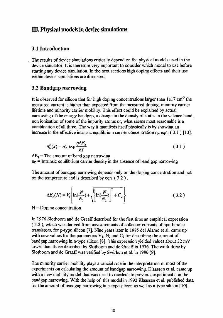
It is observed for silicon that for high doping concentrations larger than 1 e 17 cm-3 the measured current is higher than expected from the measured doping, minority carrier lifetime and minority carrier mobility. This effect could be explained by actual narrowing of the energy bandgap, a change in the density of states in the valence band, non ionization of some of the impurity atoms or, what seems most reasonable is a combination of all three. The way it manifests itself physically is by showing an increase in the effective intrinsic equilibrium carrier concentration njc eqn. ( 3.1 ) [13].
2( ) _ 2 qMg nie x - niO exp~ (3.1 )
Lllig The amount of band gap narrowing njO = Intrinsic equilibrium carrier density in the absence of band gap narrowing
The amount of bandgap narrowing depends only on the doping concentration and not on the temperature and is described by eqn. ( 3.2 ) .
AEg<N) = "+<:' ) + [In<:' ) J + C, } (3.2 )
N Doping concentration
In 1976 Slotboom and de Graaff described for the first time an empirical expression (3.2), which was derived from measurements of collector currents ofnpn-bipolar transistors, for p-type silicon [7]. Nine years later in 1985 del Alamo et al. came up with new values for the parameters V .. N2 and C2 for describing the amount of bandgap narrowing in n-type silicon [8]. This expression yielded values about 32 mV lower than those described by Slotboom and de Graaff in 1976. The work done by Slotboom and de Graaff was verified by Swirhun et al. in 1986 [9].
The minority carrier mobility plays a crucial role in the interpretation of most of the experiments on calculating the amount of bandgap narrowing. Klaassen et al. came up with a new mobility model that was used to recalculate previous experiments on the bandgap narrowing. With the help of this model in 1992 Klaassen et al. published data for the amount of bandgap narrowing in p-type silicon as well as n-type silicon [10].
18

Both are described by the same set of parameters see table ( 3.1 ). The mentioned mobility model is described in the next section [10],[11],[12].
TABLE 3.t: Model parameters to calculate the amount of bandgap narrowing in eqn. ( 3.2 ).
Slotboom and de Graaf del Alamo et aI. Klaassen et aI. (p-type) (n-type) ( n-type , p-type )
VI (mV) 9.0 9.35 6.92
N:l ( cm-3) tel7 7el7 1.3el7
Cz 0.5 0 0.5
The values for the parameters VI, N2 and C2 given by Klaassen et aI., have been used in the simulations described in this project.
3.3 Carrier mobility
3.3.1 Introduction
The mobility model described in this section takes into account the main contributions to mobility reduction such as: lattice scattering, donor and acceptor scattering and electron-hole scattering. Beside these effects screening of impurities by charge carriers and the temperature dependence of both majority and minority carrier mobility are included. The model described in this section gives the carrier mobility as a function of the donor, acceptor, electron and hole concentrations and of the temperature. This makes the model especially suited for device simulation purposes.
3.3.2 Mobility due to lattice scattering
At very low impurity concentrations the only scattering mechanism is lattice scattering. The electron mobility due to lattice scattering J..le,L as well as the hole mobility due to lattice scattering J.!h,L are both given by eqn. ( 3.3 ).
300 (J
Pi,L = P rnax (T) I (3.3 )
The subscript i stands for e ( electron) or h ( hole) while the parameters J..lmax and 9i can be found in table (3.2 ).
19

3.3.3 Mobility due to majority impurity scattering
The mobility due to majority impurity scattering: the electron mobility due to donor scattering J..le.D and the hole mobility due to acceptor scattering J,.I.h,A , is given by eqn. (3.4a).
(3.4a)
with
(3.4b)
and
= f.Jminf.Jmax ~300 f.Ji,c _ T
f.Jmax f.Jmin (3.4c)
The subscript ( i,I) in eqn. (3.4a) stands for ( e,D ) or (h,A) while ND and NA are the donor and acceptor concentrations. The parameters J,.I.max, J..I.rnin, Nrefl and al can be found in table ( 3.2 ).
TABLE 3.2: Model parameters to calculate the carrier mobility.
Parameter Electrons ( As ) Holes (B)
J.l,nax ( cml V-I S-I ) 1417.0 470.5
flmin ( cml V-I S-l ) 52.2 44.9
Nren (cm-3) 9.68e16 2.23e17
Nrer,r ( cm-3 ) 4e20 7.2e20
at 0.68 0.719
CI 0.21 0.40
9I 2.285 2.247
At high carrier concentrations carriers tend to screen impurities from other carriers. This physical process is called screening. The theory which starts from a screened Coulomb potential requires a collision cross·section for impurity scattering that depends only on the carrier concentration c. When taking the effect of screening into account the mobility due to majority impurity scattering is then given by eqn. ( 3.5 ).
20

N.", C (N) = (_l'e_,,)a l + _
Pi,l 1 Pi,N N Pj.c N 1 I
(3.5 )
From eqn. (3.5 ), because the second term in eqn. (3.5) is dominant at high impurity concentrations, it can be seen that due to screening at high impurity concentrations the mobility due to majority impurity scattering increases with the carrier concentration.
Ultra-high impurity concentrations have an effect on the carrier mobility. Above an impurity concentration of 1 e20 cm-3 the carriers are no longer scattered by impurities possessing one electronic charge and a concentration Nr , but by impurities with Z electronic charges and a cluster concentration N1' = Nr/Z . These ultra-high concentration effects can now be taken into account by replacing Ntin eqn. (3.5) by Z x Nr,.s where Nl,s accounts for the ionized impurity concentrations. Solving for Z at each impurity concentration Nr,.s yields the clustering function Zr(Nl,s) given by eqn. ( 3.6a).
(3.6a)
(3.6b)
The values for the parameters Nref,l and CI can be found in table ( 3.2 ).
3.3.4 Mobility due to minority impurity scattering
The mobility due to the minority impurity scattering, the electron mobility due to acceptor scattering J..le,A and the hole mobility due to donor scattering 1lh,D are given by eqns. ( 3.7a/b ).
Pe.D Pe,A = G(~)
Ph.A Ph,D = G(P
h)
(3.7a)
(3.7b)
The subscript e and h ofP indicate that the effective mass of electrons or holes has to be used in the equation for G(P). The effective mass for electrons Ille used in the calculations and in the simulations is equal to ~ while the effective mass for holes Il1h is equal to 1.258 ~. The parameter ~ is called the free electron rest mass. The ratio G(Pi) is defined as the collision cross-section for repulsive screened Coulomb potentials devided by the attractive screened Coulomb potentials and is given by eqn. (3.8 ).
(3.8 )
21
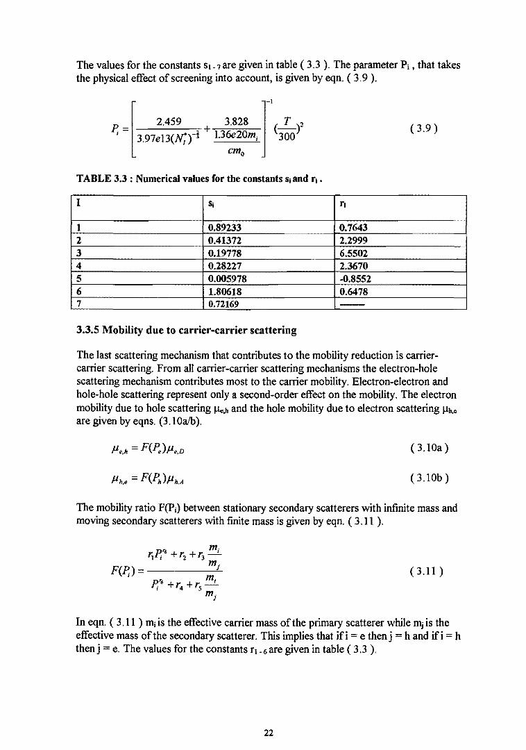
The values for the constants SI-7 are given in table ( 3.3 ). The parameter Pi , that takes the physical effect of screening into account, is given by eqn. ( 3.9 ).
[ ]
-1
P, _ 2.459 3.828 (~)2 j - 3.97e13(N;ri + 1.36e20mj 300
cmo
(3.9 )
TABLE 3.3 : Numerical values for the constants Sl and r ••
I SI rl
1 0.89233 0.7643 2 0.41372 2.2999 3 0.19778 6.5502 4 0.28227 2.3670 5 0.005978 -0.8552 6 1.80618 0.6478 7 0.72169 --
3.3.5 Mobility due to carrier-carrier scattering
The last scattering mechanism that contributes to the mobility reduction is carriercarrier scattering. From all carrier-carrier scattering mechanisms the electron-hole scattering mechanism contributes most to the carrier mobility. Electron-electron and hole-hole scattering represent only a second-order effect on the mobility. The electron mobility due to hole scattering J..le,b and the hole mobility due to electron scattering J.1h,e
are given by eqns. (3. IOa/b).
(3.IOa)
(3.IOb)
The mobility ratio F(Pi) between stationary secondary scatterers with infinite mass and moving secondary scatterers with finite mass is given by eqn. ( 3.11 ).
(3.11 )
In eqn. ( 3.11 ) mj is the effective carrier mass of the primary scatterer while mj is the effective mass of the secondary scatterer. This implies that if i e then j = h and if i = h thenj = e. The values for the constants rl-6 are given in table (3.3 ).
22

3.3.6 Total carrier mobility
All scattering mechanisms described in the previous sub sections contribute to the total carrier mobility J..li. The total carrier mobility for electrons IJe and for holes J..lh can now be described as a function of the donor,acceptor,electron and hole concentration by eqn. ( 3.12a).
-1 -1 -1 -1 -I Pi = Pi,L + Pi,D + PI.A + Pi,j (3.12a)
where
-I -I -I -1 PI,D + Pi,A + Pi,! = PI,D+A+! (3.12b)
With again the same meaning for the subscripts i and j as stated earlier. The last three terms in eqn. ( 3 .12a ) have been derived in this section for the situation where there is only one scattering partner, indeed there are three scattering partners each time for electrons as well as for holes. This gives the following expression for J..li,D+A+j eqn. (3.13a) :
= Nt,s<: (Nrefl )UI + ( n + p ) Pi.D+A+! Pi,N N N. P;,c N
l.sc,eff l,se I,se,eff
(3.13a)
where
(3.13b)
and
(3.13c)
and
N • n hsceR' == NA +G(P.h)ND +--
, ,W F(]>,.) (3.13d)
3.4 Recombination
3.4.1 Auger and Shockley-Read-Hall recombination
An important effect which occurs at high doping concentrations in silicon is Auger recombination. Due to Auger recombination a reduction in the carrier lifetime is obtained. There are two cases of Auger recombination. The first case is a recombination between an electron and hole, accompanied by the transfer of energy to another free hole. The second case is a recombination between an electron and hole that results in a transfer of energy to a free electron. The third free particle involved in this process will lose it's energy to the lattice in the form of heat. The process involving two electrons and a hole occurs primarily in a heavily doped n-type material thus in our process this would occur only in the emitter part in the epi-silicon with
23

arsenic concentrations above le20 at.cm-3• The Auger recombination is given by eqn.
(3.14 ).
( 3.14 )
The values of the Auger recombination coefficients CAu.,n and CAu.,pcan be found in table ( 3.4 ) [12].
TABLE 3.4: Parameter values for Auger and SRH recombination.
Parameter Value
2.78e-31 1.83e-31 2.5e-5 2.Se-5
The reduction ofthe electron 'tn lifetime and hole 'tp lifetime due to Auger recombination is given by eqns. ( 3 .15a/b ).
1
and
1
(3.15a)
( 3.15b )
It should be noted that due to the strong dependence of Auger recombination on the majority carrier concentration, the layer at the silicon/polysilicon interface with very high doping concentrations ( the emitter layer in the epi-silicon ) may form a so called dead layer. In this dead layer all injected excess carriers will recombine. This effect gives rise to a higher base current and thus a decrease in the gain.
It is also necessary to include Shockley-Read-Hall ( SRH) recombination in the device simulation. The Shockley-Read-Hall theory of recombination assumes that a single recombination center, or trap, exists at an energy within the forbidden bandgap. There are four different processes defining SRH-recombination. The first is the capture of an electron from the conduction band by an initially neutral empty trap. The second process is the inverse of process 1: The emission of an electron from a trap level into the conduction band of the material. The third one is capture of a hole from the valence band by a trap containing an electron. The fourth is again the reverse of the third process: The emission ofa hole from a neutral trap into the valence band. The SRHrecombination RsRH is given by eqn. (3.16a).
24

where
and
1: O.p
1:P =I+ N
NSRH,p
(3.16a)
(3.16b)
(3.16c)
The values of the parameters tp,o, tn,o, NsRH,p and NSRH,n can be found in table ( 3.4 ) [12]. The value of q8E is the difference in energy between the trap level and the intrinsic Fermi level.
3.4.2 Surface recombination
The use of polysilicon for emitter contacts allows to make shallower junctions as well as self aligned and hence smaller structures. The emitter efficiency is improved due to a reduction in minority carrier hole current which is injected from the base into the emitter for a npn transistor. A good way to describe this effect is with the help of the effective recombination velocity Sp at the surface of the monocrystalline region. The minority carrier current Jp crossing the polysilicon/silicon interface is related to Sp given by eqn. (3.17) [14],[15].
(3.17 )
p = Excess minority hole concentration at the monocrystalline silicon surface
All important aspects of the polysilicon and interfacial oxide layer related to the device characteristics are taken into account by the recombination velocity Sp as discussed in section 2.3.3. When rewriting eqn. ( 2.4 ) Sp becomes:
8 =8 +T. p I block T. +8 +8
block I poly
(3.18 )
As a result of the transport mechanisms through the interfacial oxide, Sp strongly depends on interfacial oxide thickness and the oxide barrier height ~ for holes. The ER V Sp also strongly depends on the polysilicon layer doping. Referring to Bakker et at. the dependence of the ER V Sp on the interfacial oxide thickness with the polysilicon doping level and the barrier height for holes as parameters can be seen in figure ( 3.1 ) [14],[15].
In figure ( 3.1 ) Sp has been calculated with the help of eqn. ( 3.18 ). It is noticed that Sp will asymptotically tend to Sl when the interfacial oxide layer thickness A increases
25

due to the fact that the blocking factor T block decreases with increasing .1. The device used in this project has a discontinuous interfacial oxide layer with thicknesses between o - 8 A. Therefore the only interesting part of the figure is the part where the interfacial oxide thickness is less than 8 A.
IO~ -!
"" , " " ' ,\ \\
\ \ \
\\ "
Tunnt"!in~ Jnd thc:rmillni.: t"mi~,j()n
----- x II = O,2~ t"\'
------ x" = (),~Ot"V
\ \ \ \ \ \
.\'[J = \ \ \
\ \ \ , \
\. \ \ \ \ \ ,
\ \ '\0 =
,\'0 =
.\'0 =
10 2'
10 20
10'<1
, i Sn = I 0,' 'i \ Sn =, I 0 :0 IO-iL-____ ~ ____ ~, _____________ ~ __ ~
10 20 30 -l0 50
Interface oxide thickness. A Fig. 3.1: Effective recombination velocity as a function of interfacial oxide thickness.
In figure ( 3.1 ) it can be seen that for the device used in this project, with a polysilicon doping of about 3e20 at.cm-3 as taken from SIMS measurements, the value of the ERV Sp is between the le5 and 2e5 cms· l
. An exact value ofSp can not be given, owing to the fact that Sp depends on the physical properties of the polysilicon layer and the polysilicon/silicon interface, which are known to vary significantly with doping and other processing steps. The value used for Sp in device simulations must therefore be used as a fitting parameter.
The value of Sp only influences the base current of a device and not the collector current, because it has influence on the recombination rate of excess minority carrier holes in the emitter of a npn transistor and therefore it determines the minority carrier hole concentration. The minority carrier hole concentration determines the base current of a npn transistor. Decreasing Sp decreases the base current and hence increases the gain because the collector current is not affected. Especially for shallow junctions the improvement in gain will be larger when Sp is decreased, due to the fact that the recombination in the thin mono crystalline silicon emitter region then becomes insignificant.
26

IV. Process and device simulation
4.1 Introduction
With the help of process and device simulation programs available today it is possible to accurately predict the device characteristics and behavior. For an accurate prediction of device behavior one needs measurement results and a good insight into the physical models used to characterize a device. Without measurement data an accurate prediction of device behavior can not be made, due to the fact that the simulation programs are not exactly calibrated for each different technology step.
Important measurement results used to calibrate the simulation towards the real process of the polysilicon emitter bipolar transistor described in this project are: SIMS profiles, sheet resistances and junction capacitances. Also available were the gummel plots and Hfe plots for realized polysilicon emitter bipolar transistors with different dimensions. These plots were used to calibrate and check the device simulation.
The process and device simulations are described in the following sections. In the first section the process simulation is described while in the section that follows the device simulation is described. In the above sections all simulation results discussed refer to a polysilicon emitter bipolar transistor having the smallest dimensions from which measurement results were available. The transistor used is a vertical double base NPN transistor with an emitter window of 0.9 * 0.9 ( J.lm2). In the last section the results will be checked for a polysilicon emitter bipolar transistor with different dimensions.
4.2 Process simulation
4.2.1 Introduction
The process simulator used in this project is the two dimensional process simulator TSUPREM-4, Technology Modeling Associates, Inc., Palo Alto, CA USA ( version 6.3 ) [ 19 ]. TSUPREM-4 is a TCAD ( Technology Computer Aided Design) computer program for simulating the processing steps used in the manufacturing of silicon integrated circuits and discrete devices. All different types of processing steps can be modelled. For example: Ion implantation, diffusion, silicon and polysilicon oxidation, epitaxial growth, and low temperature deposition and etching of various materials. TSUPREM-4 simulates the incorporation and redistribution of impurities in a two-dimensional device cross section perpendicular to the surface of the silicon wafer. The output information given by the program includes the boundaries of the various layers, the distribution of impurities in each layer, and stress produced by oxidation, thermal cycling or film deposition.
27

4.2.2 SIMS and simulated profiles
4.2.2.1 Introduction
Secondary Ion Mass Spectroscopy ( SIMS) provides a direct method for measuring the impurity profile of an implanted or epitaxial layer. The technique directly measures the amount of impurity in silicon as the sample surface is slowly sputtered. The sputtering removes about 40 run of the surface layer. SIMS measures electrically active as well inactive impurity levels. The big advantage of the SIMS technique in comparing it with other techniques like for example Auger Emission Spectroscopy ( AES ), Electron Spectroscopy for Chemical Analysis ( ESCA ) and Rutherford Backscattering Spectroscopy ( RBS ) is that SIMS is capable of detecting all elements and it can identifY elements present in very low concentration levels. It is therefore the most widely used surface analysis technique with the ability to measure doping level concentrations in electronic materials. SIMS is an excellent tool for generating concentration profiles of dopants in silicon at levels down to the 1 e 15 at. cm·3 range.
To apply correct impurity profiles in the process simulation, these need to be matched with the profiles measured by SIMS. Therefore it is necessary to look at the process technology steps that have an influence on the impurity concentrations. These steps include:
- Silicon and poly silicon oxidation
When growing silicon oxide, impurities that are implanted through this Si02 layer are affected. Due to this Si02 layer the implanted impurities are blocked and the concentration of the impurities underneath the Si02 layer will be less compared to a situation without a Si02 layer. The thickness of the Si02 plays a significant role, the thicker this layer, the lower the impurity concentration underneath this layer. Boron atoms will go through the Si02 layer while arsenic atoms are blocked because of their bigger size. Therefore it is very important to match the thicknesses of the different oxide layers with reality. To do this you have to change in the process simulator the time in the diffusion step used to grow the oxide.
Also the models used to grow an oxide play an important part. In the simulations the vertical model is used to grow all oxides except for the oxidation of LOCOS (LOCal Oxidation of Silicon ). To grow the 530 run thick LOCOS the viscous model has to be used. The vertical model is the simplest of the numerical oxidation models in TSUPREM-4. In this model the oxide growth is only in the -y direction and therefore the growth rate depends only on the orientation of the silicon substrate. The viscous model simulates in two dimensions viscous flow of the oxide during oxidation which allows accurate values of stress to be computed. Also the variation of crystal orientation along the interface is taken into account when calculating the oxidation rate.
28

- Implantation models. dose. energy. wafer rotation and tilt
In order to benefit from the ability to control the number of impurities implanted into a substrate, it is necessary to know where the implanted atoms are located after implantation. This information is necessary for process engineers for selecting appropriate doses and energies when designing a fabrication process sequence for new or modified integrated circuit devices. To make accurate predictions ofimplanted impurity profiles a theoretical model is needed, which is based on the energy interaction mechanisms between the impurity ions and the substrate. Within the process simulation program SUPREM-4 there are three different theoretical models to use: Gaussian, Pearson and Montecar type.
The Gaussian model specifies that a simple Gaussian distribution can be used to represent the implanted impurity profile. The simple approach of calculating an impurity profile with the help of a Gaussian distribution function does not account for several effects that occur when implants are made into single-crystalline silicon. Therefore other analytical models to calculate impurity profiles have been developed. Nevertheless, the Gaussian distribution is still commonly used to provide quick ( less simulation time) estimates of doping distributions into amorphous and singlecrystalline materials.
The Pearson model specifies that a Pearson distribution is used to represent the implanted impurity profile. This model is more complicated than the Gaussian model and therefore it gives a bettter calculation of the implanted profile. The mathematical expressions of this model fall beyond the scope of this project.
The Montecar model specifies that a numerical Monte Carlo analysis is used to simulate the implantation. This model includes the effect of reflected ions and produces damage information in the form of vacancy and interstitial profiles. In Monte Carlo analysis, ion implantation is simulated by following the history of an energetic ion through collisions with target atoms using the binary collision assumption. The calculation of each trajectory begins with a given energy, position and direction. In the simulations 1000 ion trajectories are calculated and the depth at which each ion stops is determined ( it is possible to increase this number, but that was not necessary). The Montecar model is very complicated and time consuming.
When to use which implantation model appears to have influence on the doping profile, but especially on the electrical characteristics of the device. More about this in the next section when discussing the simulation results of the impurity profiles.
It is clear that changing the implantation dose and energy most affects the impurity doping profiles. It is therefore necessary to retain the values of these two parameters as close as possible to reality. Yet in practice it is allowed to change these parameters by 20-30 percent due to physical effects that occur in reality, which are not taken into account in the simulations.
In the simulations rotation of the wafer is not included. The tilt angle was in the simulations and in reality set to 70
• The effect of the 70 tilt angles at which wafers are held to minimize channeling, is to charge the scan rate at the wafer surface so that a
29

linear gradient in the implant dose across the wafer is created. Taking tilt in the simulations into account, seems to have influence on the doping profiles but especially on the base sheet resistance ( see section 4.2.3 ).
- DtUusion time and temperature
Once an implantation step is done, it will be followed for most of the time by a diffusion step to outdiffuse the impurities in the silicon layer to create a more deeper/less steeper profile. To match the simulated profile with the SIMS profile it is sometimes necessary to change the time of the diffusion step. A change in temperature is normally avoided because this will also affect the concentrations to differ from the already implanted impurities in the silicon.
4.2.2.2 Simulated profiles
Two profiles were measured with the SIMS technique:
1) The buried-N profile, just after the epi growth and after complete wafer processmg.
2) The emitter profile, through the middle of the emitter.
The first profile checked in the simulations was the buried-N profile just after the episilicon layer growth. In the simulations the same values as in the real process for the dose and energy were used and a Pearson distribution was chosen to describe the profile. The dashed line in figure ( 4.1 ) is the simulated buried-N profile, while the solid line is the SIMS-profile.
,~ .
~. lO -= ... It! L
I;
c;:
-
Q) 10 ~ HI -;: (I
u
17 .
10
o 1100 .. . ! (,00
Fig. 4.1: The simulateq ~n~ ~I~fS .l),ur~~~-:!If profile. .' " ' .~. Ii I~t<. , "j • :'. j .:'.' ,.." •
30
1101]
Ih:·plh rnnd

In figure ( 4.1 ) there is also a plot ofthe buried-N SIMS profile and simulated profile ( dashed line) after complete wafer processing. Due to outdiffusing of the arsenic into the epi-silicon layer the profile is wider and a little lower than the buried-N profile just after the epi layer growth. The outdiffusion of the arsenic is caused by high temperature diffusion steps, especially the RTA-drive at the end of the process. As can be seen in the figure the simulated profiles are very well matched to the SIMS profiles.
The most important profile in the process of making a polysilicon emitter bipolar transistor is the profile of the emitter. Figure ( 4.2 ) shows this profile. The dashed line is the simulated emitter profile while the solid line is the profile measured with the SIMS technique. It can be seen that the doping concentration in the polysilicon layer is almost uniform. This simplifies the transport equations and it makes possible the analysis in section 2.3.
In the polysilicon layer arsenic is implanted with a dose of5e15 at.cm'2 at 30 KeV. Due to the RTA-drive at 1075 °C for 12 seconds arsenic diffuses down the grain boundaries in the polysilicon layer and after a while it diffuses into the bulk of the grains and into the monocrystalline silicon. The large arsenic concentration peak at the polysiliconlsilicon interface is caused by segregated arsenic at the pseudo-grain boundary between the polysilicon and the silicon. The peak value in the simulated profile 6e20 at. cm,3 is a little higher than the peak value from the SIMS measurements 4e20 at.cm,3.
The arsenic dose measured by the SIMS measurement technique is 3.1e15 at.cm,2, with this dose the arsenic profile is plotted in figure ( 4.2 ). The arsenic dose implanted in the real process and in the simulations is 5e15 at.cm'2. The simulated arsenic profile in figure ( 4.2) ( dashed line) gives therefore a little higher peak concentration than the arsenic profile measured by SIMS. When doing a simulation with an arsenic dose of 3.1e15 at.cm,2 the peak concentration of the arsenic at the polysiliconlsilicon interface will decrease to the same value as the peak concentration of the SIMS profile.
The above described difference in peak concentration can as described above simply be matched by lowering the arsenic implant dose. This has not been done because lowering the arsenic implant dose gives an increase in the base Gummel number On resulting in a decrease in the collector current. Also the emitter Gummel number On will decrease when the arsenic implantation dose is lowered which results in a slightly higher base current ( see table 4.1 ). Thus lowering the arsenic implant dose will decrease the transistor gain Hfe.
TABLE 4.1: Calculated emitter and base Gummel numbers
Standard/real Arsenic dose RTA temp. RTAdrive simulated 3.1e15 at.cm,l 1l00°C 20 seconds process
GE ( at.cm,l ) 2.37e14 1.40e14 JJ. 4.06e14 11' 3.94e14 11'
GB ( at.cm,l ) 5.86eI2 6.88e12 11' 4.18e12 JJ. 4.28e12 JJ.
31

The RTA emitter drive affects the diffusion of the arsenic into the monocrystalline silicon emitter part. Therefore the RTA emitter drive determines the emitterlbase junction depth, the emitter <k and base Os Gummel number ( see eqns. 4. 1 alb ) and the breakup of the interfacial oxide layer, which allows the arsenic to diffuse into the silicon.
XE = Emitterlbase junction depth in the epi-silicon XB = Base/collector junction depth in the epi-silicon
( 4.1a)
( 4.1b )
In eqns. ( 4. 1 alb ) unifonn doping concentrations in the emitter and base are assumed, but in the real process there are of course emitter and base non uniformities ( see also figure 4.2 ) and the emitter and base gummel number will therefore be given by eqn. (2.6d ). The base Gummel number determines the collector current and is therefore a crucial factor for the device simulation. The junction depths can be found in table ( 4.2 ). The calculated base and emitter Gummel numbers for an increased RTA temperature can be found in table ( 4.1 ).
1.00E+21 .....-------------------~
1.00E+20
E 1.00E+19 ~ ~ ~ \ !. .-.-' '\ ' C ." .2 1.00E+18 ! C III U a 1.00E+17 u
1.00E+16 ,- 1-. _. _. - . -" ..... r •. """ : I ' ~i
1.00E+15 +--:::-:--i-'--H---t---+--L...L.;-.L...!t'-l4lil1.L-+---+----l----l
40 140 240 340 440 540 640 740 840 940
Depth [nm]
Fig. 4.2: SIMS and simulated emitter-base profile.
TABLE 4.2: Simulated and SIMS junction depths
SIMS measurements Simulated junction junction depths depths
XE( Jim ) 0.058 0.044 XB ( p.rn) 0.33 0.35
32
The base/collector junction depth XB taken from the SIMS measurement technique can not be predicted exactly from figure ( 4.2 ). In this figure the part where the base/collector junction depth lies is difficult to accurately determine. However the simulated junction depth (exactly calculated) of 0.35 Jlm is not that much different from the value obtained from the SIMS profile from figure ( 4.2). The value for the simulated emitterlbase junction depth XE differs no more than 20 percent.
The emitterlbase junction depth XE critically depends on the RTA-drive. Increasing the RTA temperature or duration results in an increase in the arsenic out-diffusion from the polysilicon emitter and thus in a reduced base Gummel number resulting in an increase in the collector current. Increasing the R T A duration from 12 seconds to 20 seconds has the same effect on the emitterlbase junction depth XE as an increase of RTA temperature by 25°C. The emitterlbase junction depth XE increases 12 nm towards 0.056 Jlm when changing the RTA duration or temperature by these values. This has not been done in the simulations, because a reduced base Gummel number increases the base sheet resistance. The base sheet resistance is a very important parameter for this process and has to be matched with reality ( see section 4.2.3 ).
The boron profile in figure ( 4.2) determines the base profile of the polysilicon emitter bipolar transistor. In the SIMS profile only the isotope Bll ( dose 2.0e13 at.cm-2
) is measured while in the simulated profile the total boron dose was considered. The B 10
isotope concentration in the process is 20 percent of the Bll concentration (BF2 -
implant includes both isotopes) which accounts for an increase of the boron SIMS profile in figure ( 4.2 ). Taking this increase of the boron SIMS profile ( compared to the simulated profile) into account the profile will still be a little higher than the SIMS profile. This is due to the fact that the dose of the BF2 ( base )-implantation, to form the base of the npn transistor, in the simulations was increased from 2.4e 13 towards 2.8e13 at.cm-2 to obtain a better value for the base sheet resistance ( section 4.2.3 ).
A very crucial processing step is the first boron implantation in the process. The first boron implantation in the process is one with a dose 1.7e12 at.cm-2 and energy 25 KeV. This implantation is done to tune the Vt (threshold voltage) for the CMOS part ofthe process. This implantation, initially done to only influence the threshold voltage of the MOS transistors used in the process, also affects the bipolar part of the process. The influence of this implantation on the device electrical characteristics is dependant on the implantation model choosed. This will be discussed further in section 4.3.2.
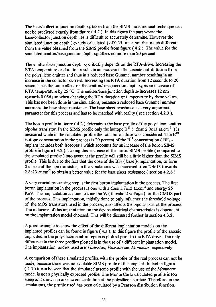
A good example to show the effect of the different implantation models on the implanted profiles can be found in figure ( 4.3 ). In this figure the profile of the arsenic implanted in the polysilicon emitter region is plotted prior to the R T A drive. The only difference in the three profiles plotted is in the use of a different implantation model. The implantation models used are: Gaussian, Pearson and Montecar respectively.
A comparison of these simulated profiles with the profile of the real process can not be made, because there was no available SIMS profile of this implant. In fact in figure ( 4.3) it can be seen that the simulated arsenic profile with the use of the Montecar model is not a physically expected profile. The Monte Carlo calculated profile is too steep and shows no arsenic concentration at the polysilicon surface. Therefore, in the simulations, the profile used has been calculated by a Pearson distribution function.
33

Most of the time the Pearson model is choosen for the different implantation steps throughout the whole process, except for implantations with energies above 200 KeV. For these implantations no Pearson tables are available in the process simulator SUPREM-4 and therefore a Monte Carlo calculation has been chosen.
1.00E+22 ...-----------------------,
1.00E+21
;;' 1.00E+20 E ~ li .... 1.00E+19 c
i i 1.00E+1B
g 8 1.00E+17
UX>E+16
I
// / i
./ !
I \. ,', . ~'~. .....
\ .... \, "\~ , ,
\ \. \ .... . "
\ '\, \ ... , \ \,
\. \'" , "
.... ············Pearson
.. _. _. _ .. Gaussian
--Montecar
. \\\ .... \
1.00E+15 1--+----.---..-+----.----:-..-----:.,---.,....----,---.,....----'
-1.8235 -1.8035 -1.7835 -1.7635 -1,7435 -1.7235 -1.7035 -1.6835 -1.6635
Depth [pm]
Fig. 4.3: The arsenic profile in the polysilicon emitter before annealing for three different implantation models.
4.2.3 Sheet resistances
One of the most important parameters to be measured during fabrication of wafers is the pinched/intrinsic base sheet resistance Roo. This is the sheet resistance of the quasineutral base under the emitter diffusion region and is directly related to the Gummel integral by eqn. ( 4.2 ).
1 ~ / sq = --W.=b---- (4.2 )
qJ1p J NAeff(x)dx o
Wb The neutral base width
Another important parameter is the extrinsic base sheet resistance ~ , given by the same eqn. as the eqn. for the intrinsic base sheet resistance (eqn. 4.2). The calculation of both the extrinsic and intrinsic base sheet resistances is a two-dimensional problem.
Both sheet resistances are very much dependent on the different processing steps. Therefore it is necessary to match the simulated sheet resistances with the measured sheet resistances to be sure that the simulations are correct. The simulated as well as the measured intrinsic and extrinsic base sheet resistances are found in table ( 4.3 ).
34

TABLE 4.3: Calculated and simulated square base sheet resistances.
Measured values Simulated values
Rt. (knlsq) 2.75 2.86
Rbe (knlsq) 9.0 8.67
The most critical step in the process for the extrinsic as well as for the intrinsic base sheet resistance is the base-implantation. In the real process this implantation is a BF2 implant of2.4e13 at.cm-2 at 40 KeV, while in the simulations the implantation dose was increased towards 2.8e13 at.cm-2 to obtain better values for the base sheet resistances. The values for the extrinsic and intrinsic base sheet resistance given in table ( 4.3 ) are those for the simulation with a implantation dose of2.8e13 at.cm-2
. In fact the value for the extrinsic and intrinsic base sheet resistance for an implantation dose of 2.4e13 at.cm-2 is 3.04 kO/sq and 9.47 kO/sq respectively.
With a dose of2.4e13 at.cm-2 the value for the intrinsic and extrinsic base sheet resistance is somewhat higher than the values with an implantation dose of2.8e13 at.cm-2
• The main reason for using a higher implantation dose in the simulations is that the extrinsic as well as the intrinsic base sheet resistance showed better values compared to reality. Also the Hfe plot gives much better values in the low injection region when using the higher dose of2.8e13 at.cm-2
. More about this in section 4.3.2 where the device simulations are discussed.
When changing the RTA emitter drive time from 12 to 20 seconds the pinched base sheet resistance increases from 8.67 kO/sq towards 12.3 kO/sq. This difference can be explained with eqn. ( 4.2). When the RTA diffusion time is increased towards 20 seconds the base Gummel number decreases 27 percent ( see table 4.1 ). This gives an increase in the pinched base sheet resistance by 37 percent towards 11.87 kO/sq due to eqn ( 4.2). This value is close to 12.3 kO/sq, and the difference can be explained by a slightly reduced hole mobility.
The situation is different when the same RT A drive time is increased from 12 seconds towards 20 seconds for a simulation in which the dose of the first boron implantation (Vt-implantation) is increased from 1.7e12 at.cm-2 towards 2.1e12 at.cm-2
• The pinched base sheet resistance for an implantation dose of2.1e12 at.cm-2 and 12 seconds R T A emitter drive time is 8.17 kO/sq. When changing the RT A emitter drive time towards 20 seconds the pinched base sheet resistance is increased towards 37.3 kO/sq. Due to the RTA drive time increase the base Gummel number decreases from 5.88e12 at.cm-2 towards 2.17e12 at.cm-2
. This results with the help of eqn. ( 4.2 ) in a pinched base sheet resistance of22.14 kO/sq. This value is more than 40 percent lower than the simulated value. This is unlikely to be due to a reduced hole mobility. This needs to be investigated further.
35

4.2.4 The role of the interface oxide break-up model in SUPREM-4
In SUPREM-4 version 6.3 modeling of poly crystalline material has been incorporated for the first time. The behavior of dopants in polycrystalline material is strongly influenced by the boundaries between crystalline grains. The rate of segregation at the grain boundaries depends on the rate of grain growth, while the number of diffusion paths along the boundaries depends on the grain size.
A thin interfacial oxide layer is typically present between a deposited polysilicon layer and an underlying single-crystalline silicon layer. This interfacial oxide layer, presents a barrier to epitaxial realignment of the poly layer. Due to the high temperature RTA emitter drive the interfacial oxide layer breaks up and a discontinuous oxide layer is formed for the device described in this project.
In SUPREM-4 a model is described in which the parameters for the model are specified in terms of a characteristic break-up time for the thinnest ( 5A) interfacial oxide layer ( see eqn. 4.3a ).
d~d = _1 (5Angstrom) 3 1
dt tbu tox .JTiN EA
Rvoid = The radius of the voids in the interfacial oxide layer
(-TBU.EJ
tbu = TBU.Oexp kT -)
tox = interfacial oxide thickness NEA = areal density ofthe voids
(4.3a)
(4.3b)
The parameter tax can be changed in the process simulator SUPREM-4, also the parameters TBU.O ( 7e-19), (a constant), and TBU.E ( -5.0), (the activation energy of the oxide break-up process), can be changed.
The above model looks interesting but only values for tax varying between 0 - 8 A had some influence on the electrical characteristics of the device. The base current was sligthly reduced for a greater value of tox . This is less significant because the value of the effective surface recombination velocity of holes in the emitter, which can be used to influence the base current in the device simulator MEDICI, appeared to have a much larger effect on the base current. The above described interfacial oxide model in SUPREM-4 needs to be updated in the future, so that it will be possible to even model a discontinuous oxide layer perfectly. Presently this model shows a better base current, but the model is not so good that it is possible to see what the influence will be of different settings of the parameters on the device electrical characteristics.
36

4.3 Device simulation
4.3.1 Introduction
The device simulator used in this project is the two-dimensional device simulator MEDICI, Technology Modeling Associates, Inc., Sunnyvale, CA USA ( version 2.1.2) [ 16]. MEDICI is a powerful device simulation program that simulates the behavior ofMOSFETS, bipolar transistors and other semiconductor devices. It makes use of the two-dimensional distribution of potential and carrier concentrations in a device. The output of the program is the electrical characteristics ofa device for arbitrary bias condition.
A number of physical models have been incorporated into the program for accurate simulation of different devices. There are models for recombination, impact ionization, photogeneration, band-gap narrowing, band to band tunneling, mobility, and lifetime of the carriers. MEDICI also incorporates both Boltzmann and Fermi-Dirac statistics, including incomplete ionization of impurities.
4.3.2 Electrical characteristics
MEDICI calculates all kind of different electrical characteristics for all kind of devices. For a polysilicon emitter bipolar transistor the most important characteristics looked at in this project are :
- The base sheet resitances - The Gummel plot - The Hfe plot
To make physical calculations it is very important to include the right physical models within MEDICI. In chapter 3 these models are discussed. The following physical effects are included in the device simulations: Bandgap narrowing, Auger and Shockley-Read-Hall recombination, finite surface recombination, Philips unified mobility model to calculate the carrier mobility and tunneling.
In figure ( 4.4 ) the Gummel plot of the device is given, while in figure ( 4.5) the Hfe plot of the device is given. In both figures the solid line is the measured plot while the dashed line ( Hfe ) or the line with the markers ( Gummel ) is the simulated plot.
To check the Gummel plot more accurate absolute values are taken from the measurements as well as from the simulations for three different operating regions ( low injection region Vbe == O.4V, linear region Vbe == O.7V and the high injection region Vbe == 1.0V) and those values are given in table ( 4.4 ).
The simulated collector current over the complete range of base emitter voltages is well matched to the measured values. This is not surprising since the collector current depends on the base Gummel number and therefore on the pinched base sheet resistance. The value of the pinched base sheet resistance in the simulations as discussed in section 4.2.3 is almost equal to the measured value.
37

By far the most important parameter for this simulation, the parameter which has the most influence on both the collector current and on the base current, is the temperature T. The exact temperature at which the measurements took place is not exactly known due to different room temperatures at different times/periods. Therefore this value is taken as 295 K. To obtain good values for the simulations the temperature was set to 293 K which is the lowest reasonable value for room temperature. The collector and base current are both increasing with increasing temperature and decreasing with reduced temperature.
0.Q1
0.001
0.0001
1 E..Q5
1 E.Q6
1E.Q7
:S 1E.Q8 .5 !i 1E.Q9 .5
1E-10
1 E-11
1 E-12
1 E-13
1 E-14
1 E-15 0.4 0.5 0.6 0.7 O.B 0.9
Vbe [volts)
Fig. 4.4: Measured and simulated Gummel plot
TABLE 4.4: Absolute values for the collector and base current.
Measured values; T = 295 K Simulated values; T = 293 K Vbc=-lV Vbc=-lV
Vbe(V) 0.40 0.70 10 0.40 • 0.70 1.0 I IdA) 2.29e-13 2.66e-9 .10e-5 4.51e-14 3.12e-9 5.99e-5
Ie (A) 4.36e-12 3.54e-7 1.23e-3 3.43e-12 3.93e-7 1.07e-3
For example when the temperature in the simulations is increased to the MEDICI default setting of300 K the collector current for a base emitter voltage of 0.7 V increases by about 70 percent, while the base current increases by 55 percent. This gives rise to an Hfe ( IJIb) increase of only 8 percent.
The values for the simulated base current see table ( 4.4 ) do not well match the measured values. Only for the linear region ( the normal operating region of a transistor) the base current is well matched. For the low injection region the simulated base current is about a factor 5 lower than the measured value, while for the high
38

injection region the simulated base current is almost a factor 3 higher than the measured value.
Naturally the value of the Effective Recombination Velocity Sp ( see section 3.4.2 ) has much influence on the base current. In the simulations a finite surface recombination velocity is taken into account. In this process only the surface recombination velocity for holes vsurJp in the emitter has influence on the base current. When decreasing this factor the base current decreases and when increasing the surface recombination velocity for holes the base current also increases. Therefore this is a parameter that can be used to affect the gain ( Hfe ) of a transistor in the simulations.
From figure ( 3.1 ) in section 3.4.2 it can be seen that for the process described in this project the recombination velocity has a value between 1 e5 and 2e5 cms·l . The value used in the device simulation is 1.4e5 cms·I
, a value in good agreement with other authors [14],[15]. The level of the gain has been matched by changing the value for the effective surface recombination velocity. This has been done for the linear region, because this is the normal operating region of the transistor.
160
140 .-----. ,,;- "- . . ...
12.0 / .... ..... ,
" 100 I '\
~ I \ '5 80 \ .::. I S . ::E: \
60 . \ .
40 \ . \ .
20 \
0 N .... 0 ~ 9 q ~ ~ q ~ ~ .... .... .... t.iJ t.iJ t.iJ w w w w w w w w .... .... .... .... .... .... .... .... .... .... ....
Ie [A]
Fig. 4.5: The simulated and measured Hfe plot
In figure ( 4.5) the measured and the simulated Hfe plot are shown. The Hfe ( f3 = Ie I Ib ) plot can be divided in three separate regions: The low injection region, the normal operating region of the transistor and the high injection region.
In the low injection region, at low forward bias of the base-emitter junction, the current gain f3 will be reduced. This is due to the fact that at low forward bias, there is an important additional component of base current due to recombination of excess carriers inside the emitter-base space charge layer added to the normal base current. Therefore the base current increases at low forward bias of the base-emitter junction and the gain automatically decreases because the collector current is not affected.
39

Especially in the simulated Hfe plot there is a slight fall off of the gain in the normal region of operation. The reason for this falloff is due to the so called reverse Early effect. At high base-emitter voltages the emitter-base depletion layer decreases which increases the base Gummel number due to an increased effective base width. An increased base Gummel number accounts for a less dramatic increase in the collector current at high base-emitter voltages. Therefore the gain is slightly reduced for higher base-emitter voltages.
This slight falloff of the gain in this ideal region of operation can be reduced by performing a simulation without taking the effect of band-gap narrowing into account. When doing a simulation without bandgap narrowing and by stating infinite surface recombination in the emitter there is almost no fall off of the gain at higher baseemitter voltages.
The effect of bandgap narrowing increases the effective intrinsic equilibrium carrier density eqn. (2.6c ), it decreases the effective doping concentration in the emitter eqn. (2.6b ) and therefore the base current is increased eqn. (2.6a). In the simulations the base current is increased by a factor 40 when taking bandgap narrowing into account. The collector current is only increased less than by a factor 2 with bandgap narrowing. Therefore the gain is decreased more than a factor of 20 with bandgap narrowing taken into account.
The decreased gain due to the effect of bandgap narrowing can be compensated by taking finite surface recombination in the emitter into account. Finite surface recombination of the minority carrier holes in the emitter decreases the base current and has no influence on the collector current. Therefore the gain is increased when using finite surface recombination of holes in the emitter instead of infinite surface recombination of holes at the emitter contact.
The reverse Early effect has more influence when the base doping is higher. Bandgap narrowing is a high doping effect and has influence for doping concentrations larger than lel7 at.cmo3
• For the high doping concentrations in the thin epi-silicon emitter part of the structure these two effects have much influence. The slight fall off of the gain in the ideal operating region due to the Early effect can therefore best seen in the Hfe plot where the effect of band-gap narrowing is neglected. In the other plot, the plot with bandgap narrowing, the effect of bandgap narrowing and the Early effect both account for the reduced gain for higher base-emitter voltages. A simulation without taking the effect of bandgap narrowing into account is indeed not physically allowed. The effect of bandgap narrowing is nowadays very well understood and has to be taken into account in the simulations.
The strong fall off of the gain in the high injection region is due to the Kirk effect. The actual mechanism of the Kirk effect consists in a vertical widening of the effective neutral base region due to a decrease in the collector-base depletion layer. The decrease in the collector-base depletion region is much stronger than the decrease in the base-emitter depletion region due to the inverse Early effect. Therefore the base Gummel number is much more increased for the Kirk effect than for the inverse early
40

effect. The collector current decreases and hence the gain decreases by a factor of2 or 3 at high level injection.
The curve of the simulated Hfe plot figure (4.5) shows fall off of the gain in the low injection region, fall off of the gain in the normal operating region of the transistor and a strong fall off of the gain in the high injection region. Comparing the simulated Hfe plot with measured values differences can be seen.
The fall off of the gain in the high injection region due to the Kirk effect for the simulated curve is simular to the measured curve except that the fall off starts for the same collector current but only with a lower Hfe. This is due to the fact that the fall off of the gain in the normal operating region of the transistor is much more for the simulated plot than for the measured plot. This effect, as stated before, can be overcome by doing simulations without bandgap narrowing and taking an infinite surface recombination into account.
Furthermore the fall off of the gain in the low injection region for the simulated curve starts at a collector current much lower than the onset of falloff for the measured curve. This problem can possibly be solved by taking an higher effective recombination velocity in the simulations into account at the surface of the emitter base depletion region. Simulations with changing the effective recombination velocity, only at this position in the structure, have not been done. This is indeed recommended for future work.
In the simulations the fall off of the gain in the high injection region was always very well present for all kind of changes in the process technology steps. The problem in fact is the fall off of the gain in the low injection region. The falloff of the gain in this region, due to increased base current, is much dependable on the different steps in the process simulator SUPREM-4, like implant doses, ditfusion times and models chosen.
From the simulation results it appears that the processing step with the biggest influence on the fall off of the gain in the low injection region is the first boron implantation in the process ( dose 1.7e12 at.cm-2
, energy 25 KeV). This boron implantation is done to tune the threshold voltage for the CMOS part of the process. It is very interesting that the simulations show this implantation to have much influence on the bipolar part of the process.
The implantation model chosen to simulate this boron implantation accounted for the difference in falloff of the gain in the low injection region, but it had no influence on the normal operating region of the transistor or on the high injection region. The only way to get a correct Hfe plot was by choosing the Montecar model for this implant.
A simulation was done with two equal SUPREM-4 input decks, the only difference was the implantation model for the first boron implant. The results can be seen in figure ( 4.6). The Hfe plot with the Montecar model for this boron implantation is already shown in figure ( 4.5 ), this is re-plotted to show the differences with the other models. When using the Pearson model in MEDICI, the falloff of the gain in the low injection region starts for a collector current a factor 100 lower compared to the Monte Carlo model. This is not realistic anymore compared to the measured profile.
41

Also important to get a correct Hfe plot, when using the Montecar model for the threshold voltage adjust boron implant, as well as the BF2 implant to create the base of the transistor. In the real process this implantation is done at 2.4e13 at.cm-2 at 40 KeV. The Hfe plot when using these values for the base implant with the Montecar model for the first boron implant can be seen in figure ( 4.6 ). This plot also shows a fall offin the low injection region for much lower collector current compared to the dose of 2.8e13 at.cm-2. Furthermore the base sheet resistances showed better values for this increased dose, therefore this dose was choosen for the simulations.
The implantation dose of the first boron implantation ( Vt - adjust) seemed to have influence on the Hfe characteristics. Increasing this dose showed a fall off of the gain in the low injection region for even higher collector currents and showed a slighter fall off of the gain in the ideal region. This dose was not increased otherwise the pinched base sheet resistance became much too low.
160
140
120
100
:is' ~ 80 .!! ::r:
80
40
20
0 N .... 0
~ ~ I'-~ l$ q I") N .... ... .... q q q • • I
U! U! U! U! U! w U! U! U! w U! ... .... .... .... .- ... .... .... ... ... .... Ie [A]
Fig. 4.6: Simulated Hfe plots for different process parameters
A closer look at the first boron implantation is clearly required. In the real process this implantation is done for the CMOS part of the process, but the simulations showed much influence on the bipolar part of the process. Therefore experiments have to be done on real silicon to see what influence in reality this process step has on the behavior of the polysilicon emitter bipolar transistor. With this information the bipolar part of the BIMOS-3 process can be further optimized.
4.3.3 Junction capacitances
The base doping profile can be confirmed by simulating and measuring the base-emitter Cbe and for a part the base-collector Cbc junction depletion layer capacitances, which are determined by the net active doping concentration in the base. The simulated as well as the measured base-emitter and base-collector junction depletion layer capacitances can be found in table ( 4.5) for a 0.9 * 0.9 J.1m2 emitter window.
42
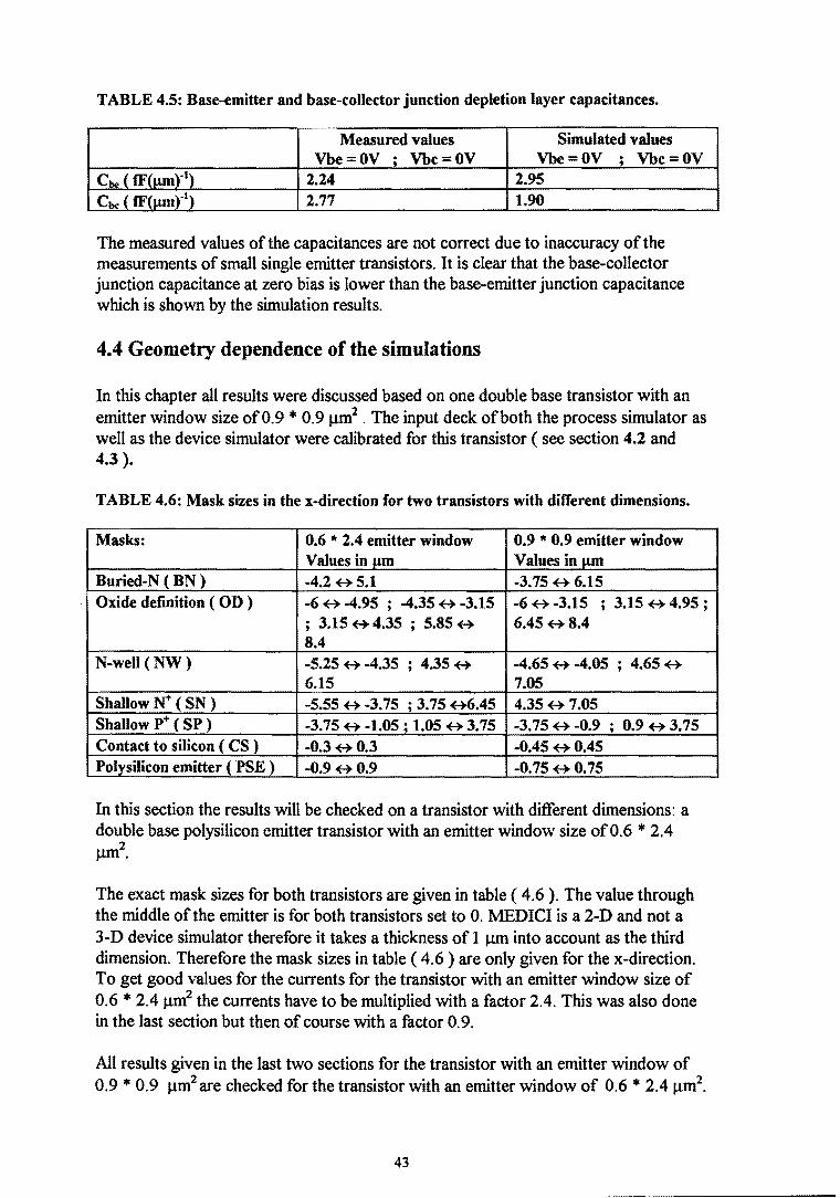
TABLE 4.5: Base-emitter and base-collector junction depletion layer capacitances.
Measured values Simulated values Vbe=OV ; Vbc=OV Vbe=OV ; Vbc=OV
Coo ( tF(~rJ) 2.24 2.95
Coo ( tF(J.tmr1) 2.77 1.90
The measured values of the capacitances are not correct due to inaccuracy of the measurements of small single emitter transistors. It is clear that the base-collector junction capacitance at zero bias is lower than the base-emitter junction capacitance which is shown by the simulation results.
4.4 Geometry dependence of the simulations
In this chapter all results were discussed based on one double base transistor with an emitter window size of 0.9 * 0.9 J..Ull2 . The input deck of both the process simulator as well as the device simulator were calibrated for this transistor ( see section 4.2 and 4.3 ).
TABLE 4.6: Mask sizes in the x-direction for two transistors with different dimensions.
Masks: 0.6 1r 2.4 emitter window 0.9 1r 0.9 emitter window Values in J.tm Values in J1m
Buried-N ( BN ) -4.2 ~5.1 -3.75 ~ 6.15 Oxide definition ( OD) -6 ~ -4.95 ; -4.35 ~ -3.15 -6 ~ -3.15 ; 3.15 ~ 4.95 ;
; 3.15 ~ 4.35 ; 5.85 ~ 6.45 ~ 8.4 8.4
N-well (NW) -5.25 ~ -4.35 ; 4.35 ~ -4.65 ~ -4.05 ; 4.65 ~ 6.15 7.05
Shallow ~ ( SN ) -5.55 ~ -3.75 ; 3. 75 ~6.45 4.35 ~ 7.05 Shallow p+ ( SP ) -3.75 ~ -1.05; 1.05 ~ 3.75 -3. 75 ~ -0.9 ; 0.9 ~ 3.75 Contact to silicon ( CS ) -0.3~0.3 -0.45 ~ 0.45 Polysilicon emitter ( PSE ) -0.9 ~ 0.9 -0.75 ~ 0.75
In this section the results will be checked on a transistor with different dimensions: a double base polysilicon emitter transistor with an emitter window size of 0.6 * 2.4 J..lm2.
The exact mask sizes for both transistors are given in table ( 4.6 ). The value through the middle of the emitter is for both transistors set to O. MEDICI is a 2-D and not a 3-D device simulator therefore it takes a thickness of 1 J..lm into account as the third dimension. Therefore the mask sizes in table ( 4.6 ) are only given for the x-direction. To get good values for the currents for the transistor with an emitter window size of 0.6 * 2.4 J..lm2 the currents have to be multiplied with a factor 2.4. This was also done in the last section but then of course with a factor 0.9.
All results given in the last two sections for the transistor with an emitter window of 0.9 * 0.9 J..lm2 are checked for the transistor with an emitter window of 0.6 * 2.4 J..lm2.
43

All simulation results appeared to be the same as the measured results with some differences mentioned in the next paragraphs.
The Gummel plot and the hfe plot for this transistor with larger dimensions showed that the electrical characteristics were are also well defined with the same input decks used in the simulators SUPREM-4 and :MEDICI. Although MEDICI and SUPREM-4, two-dimensional device and process simulation programs are, dependent on the thickness can be neglected for this structure. This is also known for the real process where transistors with different dimensions were measured. Only for a transistor with a very large emitter window size, for about 10 J..lm * 10 J..lm, there was a difference in gain.
For such a big transistor, not readily used for manufacturing, the edge capacitance can be neglected. This gives a decrease in current gain (Hfe) going from 135 for the normal size emitter window transistors, as the ones discussed in this project, towards 100.
To get the correct level of gain (about 135) for the simulated 0.6 * 2.4 J..lffi transistor, the effective surface recombination velocity for holes in the emitter had to be changed. The value was changed from 140.000 cms· l towards 220.000 cms· l
. This states for a dependence of the ERV on some mechanisms which contribute to the device emitter and base current which are dependable on the emitter dimensions, like edge capacitances which become important in structures with small emitter dimensions. This needs to be investigated more in the future.
44

v. Statistical experiment
5.1 Introduction
Especially for process engineers it is interesting and extremely beneficial to see what the influence of some process parameters is on the electrical behavior of a device.
In the process of making a polysilicon emitter bipolar transistor there are a few important process parameters which are known to affect the electrical behavior of a device. In the experiment, described in this chapter, the influence of 4 critical process parameters on the electrical behavior of the device have been investigated. These parameters are:
- The base implantation energy - The base implantation dose - The etch-back of silicon underneath the polysilicon - The temperature of the RTA emitter drive in
It should be clear to the reader that the base implantation dose and energy are important process parameters with much influence on the currents within the device. There will always be a little etch back of epi-silicon when polysilicon is deposited. Measurements showed that this etch-back influences the device behavior and therefore this parameter is taken into account in the experiment to quantify it's influence on the electrical behavior. As known from chapter 4 the RTA emitter drive temperature is critical for the device behavior.
Two important parameters the polysilicon implant dose and energy are not taken into account because it is known that they have much influence on the effective recombination velocity as can be seen in figure ( 3.1 ). The exact dependence of the ERV on the polysilicon implantation is still not known and therefore not taken into account in this experiment.
5.2 Design of experiments
First of all a design of experiment had to be chosen. The choice for a design depends on the information needed and especially for this experiment it was important to reduce the amount of experiments ( simulations) as much as possible because of the long simulation time (== 10 hours CPU time per simulation). To gather enough information from the simulations for a good estimation of the quadratic effects and interactions between two parameters, a Box-Behnken design was chosen [ 17].
The experiment is a 4-factors 3-level Box-Behnken design. This means that for the 4 factors ( process parameters) from section 5.1 three values are chosen: A high value ( + 1 ), a default value ( 0 ) and a low value ( -1 ). The exact values chosen to run this experiment can be found in table ( 5.1 ).
45

TABLE 5.1: Settings for the process parameters.
Factor low setting (-1) default setting (0) high setting (+1) standardized settin2 enerln' ( Ke V ) 35 40 45 dose ( at.cm-1
) 2.24el0lJ 2.80el013 3.36e1013
etch back (nm) 0 10 20 temperature ( °C ) 1050 1075 1100
The standard 4-factor 3-level Box-Behnken design consists of27 simulation runs. From these 27 runs three runs are performed in the center point. For a computer experiment this center point is the run with the default value for all 4 factors. This run has to take place only one time in a computer experiment, in contrast to emperical experiments. Therefore the computer experiment consists of25 runs. Note that when estimating every point in the simulations 34 = 81 runs are necessary. A Box-Behnken experiment indeed gives a good approximation with only 25 runs ( see table 5.2 ).
TABLE 5.2: Settings ofthe process parameters for the 25 runs used in the experiment.
Energy ( Ke V ) Dose ( at.cm -1 ) Etch back ( nm ) Temperature ( °C )
1 40 2.80el013 0 1050 2 40 2.24e10lJ 10 1050 3 35 2.80el013 10 1050
45 2.80e1013 10 1050 40 3.36el013 10 1050 40 I " on'10U 20 1050 40 2.24el013 0 1075
8 35 2.80e1013 0 1075 9 35 2.24e1013 10 1075 10 45 2.24el013 10 1075 11 35 3.36el013 10 1075 12 45 3.36el013 10 1075 13 40 2.24e1013 20 1075 14 35 2.80e1013 20 1075 15 45 2.80e1013 20 1075 16 40 3.36el0lJ 20 ~ 17 40 2.80el013 0 18 45 2.80el013 0 1100 19 40 3.36el013 0 1100 20 40 2.24el0lJ 10 1100 21 35 2.80e1013 10 1100 22 45 2.80el0u 10 1100
123 40 3.36el013 10 1100 24 40 2.80e1013 20 1100 25 40 2.80e1013 10 1075
46

Run 25 from table ( 5.2) is the run with the default settings of the four process parameters. This run was optimized with the help of measurement results described in chapter 4.
To run this Box-Behnken experiment the TCAD program NORMANIDEBORA (IMEC, Leuven, Belgium) was used [ 18]. Only the NORMAN part of the program was used for handling the experiment runs, the analysis of the data was done with an additional statistical program called STATISTICA instead of DEBORA.
Optimizing a process technology involves finding an optimum set of parameter settings such that a number of relevant results meet predefined targets. The methodology implemented in NORMAN for solving this problem is based on systematic application of the concepts of statistical DOE ( Design Of Experiments ) for planning a number of experiments for different settings of the input factors.
NORMAN does have a fair number of built-in DOE such as the composite designs (CCF, CCC, CCI), Plackett-Burman, Taguchi and Latin-hypercube designs, random, grid and diagonal designs, 3-level full factorial, Box-Behnken, etc. As stated earlier for the experiment described in this section a 4-factor 3-level Box-Behnken design was chosen. When using the 4-factor 3-level Box-Behnken design built in NORMAN a design is made consisting of 57 runs, this is clearly wrong based on the theory of BoxBehnken !!!![ 17] Therefore the built in Box-Behnken design was not used instead the 25 runs in table (5.2) were used.
The input file of NORMAN [RNR-G-97x-034 ; Philips, internal report] consists of three parts:
- Definition of the settings of the process parameters - Definition of the simulation path - Definition of the process and device simulation input decks
The first part describes the settings of the process parameters as can be seen in table (5.1 ). The second part describes which DOE has to be used and handles the input and output of the process and device simulator programs. The third part consists the device and process simulator input decks.
5.3 Analysis of the experiment results
5.3.1 Introduction
For a full description of the analysis see internal report [RNB-E88-97/288 ].
The responses looked at in the experiment are the base current lb, the collector current 1: and Hfe. The relation between the currents and the base-emitter voltage is an exponential function known as the pn-junction formula. Therefore the logarithm of the responses are analysed.
47

At each Vbe setting (25 settings between 0.4 and 1.0 V) a model per response is built. All effects that significantly influence the response for at least one setting of Vbe are adopted in the models per Vbe setting. This results in 25 models for each response. Each effect ( main linear, main square or interaction) has its own coefficient, depending on the Vbe setting taken into account. In the next sections the models for all three responses are discussed.
5.3.2 Base current
5.3.2.1 The base current model based on a Vhe between 0.4 and 1.0 V
Building a model for the log of the base current results in a model including the mean, the energy (A), the square of energy (A2), the dose (B), the etch back (C), the square of etch back (C2) and the temperature (D). The interactions between energy and dose (AB), energy and etch back (AC), energy and temperature (AD) and dose and etch back (BC) also differ significantly from zero. In table ( 5.3 ) the coefficients of these effects as function ofVBE are shown.
TABLE 5.3: Coefficients for In ( Ib )
effect coefficient mean -34.862-48.751 *VBE+266.985*VBE2-427.895*VBE3+360.815*VBE4-125.947*VBEs
A -4.561 +29.167*VBE-70.055*VBE2+78.958*VBE3 -41.002*VBE4+7.491 *VBEs
A2 11.486-71. 798 *VBE+ 180.687*VBE2 -228.914*VBE3+ 145.535*VBE4-37.007*VBEs
B -7.796+52.574*VBE-139.443*VBE2+181.888*VBE3-116.868*VBE4+29.658*VBEs
C 14.126-88.467*VBE+217.167*VBE2 -261.116*VBE3+ 153. 761 *VBE4-35.454*VBEs
C2 18.541-116.889*VBE+294.043*VBE2-367.882*VBE3+228.665*VBE4-56.481 *VBEs
D -1.561+10.585*VBE-30.438*VBE2+46.4*VBE3-36.656*VBE4+11.74*VBEs
AB O. 775-1.017*VBE-8.001 *VBE2+23.556*VBE3 -23.461 *VBE4+8.149*VBEs
AC -10.092+53.522 *VBE-I12.596*VBE2+ 116.721 *VBE3 -59.375*VBE4+ 11.819*VBEs
AD -1. 719+8.026*VBE-13.994*VBE2+ 11.315*VBE3 -4.367*VBE4+o. 75*VBEs
BC -13.959+90.794*VBE-232.781 *VBE2+293.917*VBE3-182.544*VBE4+44.546*VBEs
The coefficients in table ( 5.3 ) are based upon the standardized settings of the parameters. This means that the low values of the parameters have value -1 , the default setting has value 0 and the high setting has value 1.
This model fits well, as also shown by the performance indicators R2, which denotes the percentage of variation explained by the model, and R
2adj, which adjusts R2 for the
number of estimated parameters. For this model we have R2 = 0.9996 and R2adj =
0.9996. This is also shown in figure ( 5.1 ), where the observed and predicted In(Ib) are plotted against each other.
When the residuals are investigated, it is clear that the model fits better for higher Vbe values ( figure 5.2 ). Clearly there still remains some systematic effect, not adopted in the model. This is probably due to a lack of fit of the models per Vbe setting and due to building the overall model for all Vbe settings.
48
: :: f ! ! I I I I
-10 ....... --.+ ................ +-........ - .. 1 .... --.......
1
1 •• -.-......... t· .. _ .. ···· ; ....... -.... . ! i! i! 1 • I ••
·14 ••• .... ----·+ ......... -.. .-...... -.. t··-.............. -...... 1 .... · .. - .. -..... ··· .. t .. ·-.... _.-_ ..... ~ _ .............. j-_ ............... -I I ! ! I I ! i ! i ! !
;e ·18 ••• __ ..... J. ••••••• _ •••••• J. •• _._ ....... 1................ . ............. 1...---..... 1 ........... -. _c I I I I I i f iii
11 I!!!!! j ·22 ··---.. ···t·· .. · .. · .. · .. ···t······ ... ······ i · .... ·· .... ····,.-... · ... ···· .. r--········r--· .. ······ ; I ! Iii
.26' I... ···· .. ·········T····· .... ······· i ················j'· .. · .... ·······T .. ······· .. ····r-.. · .. ···· .. ·1············· .. ·
! i j ! ! ! -30 • .. •• .......... • .... T ........ _ ........ • ...... 1'· ........ • .............. · .... ·1"' .......... · .... · .... · ........ r ................ · ........ _ .. l"' ...... · ............ _-! i ! i i i : ; ! !
.~~----~----~----~----~----~~----~--~ .~ ·30 ·26 ·22 ·18 ·14 ·10
In(lb)
Fig. 5.1: Observed versus predicted In (Ib)
1.8 ,........~~..,..-........ -.,....~~--.-..,......~--r-~---.--..,......--r--..--, ! i I I ! ' ! : ! :
1.4, .. ••••••• .. • .. ·! .... • .. •·· .. ·· .. ·!· ............. ·t· .. ·· .... ·· .. ··r·· .. · .. - .. · .. l· .. ··· .... ······t·_· .. · .. ·· .. · I .. ,.
1.0 •• .. ··.!· .. ;··t-············ .. -[-..... ·· .... ···-j--··· .. ·········t········· .. ·····[······ .... ··· .. ·t .. ········· .. .. i 0.6 • .... ····-l· .. ·········-... ······ .... ·· ........ ···· .. ·· .. -r .. ·· .... · ....................... + .............. .
! 02 -HI' '''ILITh-, ~-;·~·-;+~-0h-;-:-h-,-i ~:2 ·· ..... ·S· .. t .. I..·· ·······!·· ...... ·······"1"·· .... · .. · .. ···1'··· .. · .. · .. ····1·· .. _ .. ··· .... 1'-.......... . ,!!,.. • : : : : I • iii ~.6 •• .. ••••••• .. ·+ .. · ... ······ .. · .. ··········· .. · .. 1 .... • .. ·········+ ............... +-............. +-_ ....... ... :J .: : : ; : : j : I : : : : ~ -1. 0 - ........... L ........ _ ... ,L ............... L .............. l. ......... __ .L. ........... -l .......... _.
! ! ! ! ! ! i i ! : I :
.1. 4 ••••• ...... ···..j· .. •• .... • ... ····f········ .. ······i .... ···_· ........ ·· ........ ·· .. f ...... · .......... ·• ......... ···-Iii! ! I i I , • • • ·1.8 '--___ -'--_~ ....... ___ -L-___ --'-___ .......... __ --'-___ ........
0.35 0.45 0.55 0.65 0.75 0.85 0.95 1.05
VBE
Fig. 5.2: Residuals versus Vbe when predicting In ( Ib )
In the nonnal operating region of the transistor the base-emitter voltage is 0.66 V. For this value of Vbe it is nice to see, when changing the 4 process parameters, what the influence is on the base current. Therefore the sensitivity codes are plotted in figure ( 5.3 ) for only those parameters who's interaction has influence on the base current ( see table 5.3 AB, AC, AD and BC). Note that the sensitivity plots are based upon a model predicting Vbe in the range [O.4V, 1.0 V].
49
5.3.2.2 Conclusions
With a base implantation energy lower than the default value the base current increases with increasing base implantation dose. This is due to the fact that a higher base implantation dose increases the base current due to a higher recombination rate in the base and to a possible decreased emitter gummel number. With a base implantation energy above the default value a reduced base current is observed when the base implantation dose is increased. This effect can probably be described towards an increased emitter gummel number.
With increasing RTA drive temperature the base current increases. With increasing temperature the emitter gummel number increases which counts for a decreasing base current. Therefore the effect of increasing temperature will have more effect on the recombination rate in the base then on the increase of the emitter gummel number. Therefore the base current increases with increasing RTA drive temperature.
The sensitivity plot of energy and dose and energy and etch back show saddle points. For the factors dose and etch back the result is that the base current increases with decreasing dose. For constant dose, the base current is lowest at the default setting of the etch back (10 nm).
50

With band gap narrowing PredIcted baM _ ("10"-10)
etdI_and~_"'~
1.0 ; •• -.•• -•. -""",,= •• -,,~ .. ,-• .,., -----~-_--" •• ,-•• -••• .,..I.-... ~ .. -... -.. '""';"'--,
'.
0.5
i 0.0 -6.4 -- 6.5 ..... 6.6 •• - 6.1 •..• U -- 6.9 · .... 1 -' -7.1
~ -u a L-..:.c..-...L-___ ,........, ...... _...:...._..L-....... -L. __ .;...--''--'"-,, ___ ..J ..... 7.3 ·1 .• 1.0 .0.5 0.0 0.5 1.0 •. - 1.4
-rtf
PredIcted bese .......-t(·10"-10) _ and etch _dela'"
1.0 r-o:---..,.\-\.-.... ~.----..------..:-•• -----........, •• " .. 't .......... .
·--l···"'·:::·=t~=-=: 0.5
........ d ....•.......... ;~Uh .............. u ••••••
~ , -6.4 -- 6.5 ..... 6.6 _.- 6.1 _ •• e.e
e.9 \ =~ , ••• ••••••• 7.0 -- 7.2
.1.0 "".'--___ -"'--__ "-_ ....... __ .;;:.._--''--___ ..... '" ..... 1.3 ·1.0 .0.5 0.0 0.5 1.0 ... 1.4
-rtf
Predlctedbese_("1O"-lO) _ and l""'POfll\lftdell'" ~
1.0 rT-"-.....-:r-o;;---.....,,..-----'"""""!----_, \ " \1 ""
:-
0.5 '" ·•• ...... ·\ .... · .. r\; .. ····· .. ~·~·:::·:I;-,,~ !.~ :::.~:::.:.::..t..::..".'"'.-- .•. ::-.. : .. V J i' i i.··
1 0.0 .. >L< ......... !. ... ;~,.:~ ............... .! ................. :.<:.~+~:.~.~.~~.~.:.~~ i ~ ....... < j (1.3! / ! -=:::
.. ' ... , i 1 \ : I =-~ ::; ..0.5 ···;·;.:.·";·..:.· ... --·-··i·'!':'··~· ?'.~._ .... :.:.:.~.::.~ ..... H ......... :",: .... + ... ·.4 7.2 ........ u _ ....... 6.8
if... .. i \ 7.1:::: ;.9
.. l ! "" \1. '\ \ -= ~~ 1 a '-:----_-:-: ____ ---:'--__ ...... _~_....l-...l.....J •• _. 7.3 •. ·1.0 .0.5 0.0 0.5 1.0 ••• 7.4 -
PredlctedbaM_("IO"-IO) _andl""'POfll\lftdel ....
1.0 r.-.• -.-.. -. -.. -.. -.-.. :,,' .. -. -.. -.. -.-.. -.-.. -. "1:-' .:.:-•• :.:-: •• -=-.• :-:.':': .. :-:.:'!. ,7 •• :-:.":': •• :":.::': •• :-: •• ::-:.":': •• :-:-:l. : : : : : i __ --+----~----i----
: ::"~:-l:::-·:+---·-·t--·---e.4 -- 6.S -_. 6.6
.0.5 ··~·=~~~~·~~.l:~: .. :::-:l~~==~.!· __ _ ·1.0 ••••••
·1.0 .0.5 0.0 0.5 ---. 6.7 •• - e.6 -6.9 .... ·7 -1.1 -- 1.2 '-1.3
1.0 ... 1.4
Fig. 5.3: Sensitivity curves for the base current modeled for Vbe between 0.4 V - 1.0 V
51

5.3.2.3 The base current model based on a Vhe between 0.6 and 0.7 V
Since the base current is not well modeled in the simulations for comparison with measured results over the whole range of base-emitter voltages a new model is made for a smaller range ofVbe between 0.6 V and 0.7 V. The base current was not well modeled in the simulations for the low and high injection regions see table ( 4.4 ). The coefficients for the new model can be seen in table ( 5.4 ). The coefficients as function ofVbe (between 0.6 V- 0.7 V) are approximated by a 2nd degree polynomial while the coefficients as function ofVbe (between 0.4 V - 1.0 V) are modeled by a 5th
degree polynomial.
TABLE 5.4: Coefficients for In ( Ib ) for Vhe between 0.6 V and 0.7 V.
~ coefficient
me -46.701+38.191 *VBE+O.948*VBE1
A 0.325-0.767*VBE+O.485*VBE1
B 0.05-0.165*VBE+O.12*VBE1
C 0.049-0.237*VBE+O.255*VBE1
C2 0.369-0.843*VBE+o.52*VBE1
D -0.115+O.402*VBE-0.303*VBE1
AB 0.308-1.018 * VBE+O.747 * VBEl
AC -1.007+2.453*VBE-l.518*VBE1
The fit of this model is shown in figure ( 5.4 ), where the predicted In(Ib) is plotted versus the observed In(Ib). It is shown that this fit is very well.
-19 .--------------------~
-20
§' -21
:s ~ £ -22
-23 .
-24 LL-___ "--___ -'--_______ -'--__ _
-24 -23 -22 -21 -20 ·19
In(lb)
Fig. 5.4: Observed versus predicted In ( Ib ) for Vbe between 0.6 V - 0.7 V
The sensitivity curves for Vbe = 0.66 V for this model are given in figure ( 5.5 ). These plots are more reliable than the plots for the Vbe range between 0.4 V - 1.0 V because of the better modelled base current in this operating region of the transistor.
52
5.3.2.4 Conclusions
For a given implant energy level, the base current will increase when the dose decreases or the temperature increases. With increasing R T A drive temperature the base current increases. With increasing temperature the emitter gummel number increases which counts for a decreasing base current. Therefore the effect of increasing temperature will have more effect on the recombination rate in the base then on the increase ofthe emitter gummel number. Therefore the base current increases with increasing R T A drive temperature.
The sensitivity curves of energy and etch back show a saddle point.
53

Predded base et.mII1I ("10"-10) etch back and lempera\IH default
1.0 r---:----:----,---:-----r---:----....,-• ........, 1 I,"
0.5 · .... I····· .. ···· .. ·J .. · .... · · ...... · .... · .. ·1 ...... '1/. ...... · .... .[·· .... -:;-·/ .... ·· .. · .. ! 0.0
-0.5
· · · . . I
-6.2 -- 6.3 ..... 6.4 ••• 6.5 '-·8.S -6.7 ..... 6.8 -S.9 -- 7 ..... 7.1 ••• 7.2 • •• 7.3 ·1.0
·1.0 '0.5 0.0
"""'IlY
0.5 1.0 -7.4
Predded base et.mII1I doH and etch back default
1.0.--------., ____ -:-________ --.--.
'~ '~ '" ~ "\ j', ." . '" .
0.5 ..........•......••.. ..l .......... ~ ........... l. ....... ~.: ............... l ...... :.~ ............. .. ! ,,: " . " ; ",' ,
I ~: ~ ..................... : ........ : .............. · ...... · .. · ......... ~·t~~:l··:·<.:,... = 11
~" :~:~J .1.0 '--_'--__ '----''--__ '--~ ___ '---...:.. __ ---J •• - 7.3
·1.0 -0.5 0.0 0.5 1.0 - 7.4
"""'IlY
1.0 r------!"'""""''''' .. :;:" ... c-.. -... -... -.. -... '.jc-... -... -.. -... -.•. -.. -... -.. ~ .. :'''::r:-::::=:::":'"':::-:.:-..... -... -... -... -.. ' ..
0.5 ........ · ............ ·1 S.9 .................... 1" ....... =.=.=.+.::.=.=.::: .. . ) 0.0 1'." ... ".: ................ .;' .. ""' ..................... 1 ... -(7.0 .............. :.1 .. /-<.~.~ ...... ;.:.. :::-. ::! v ••• 6.5
L .... \~ ........... l .......... L........ ~:= H " ;\ \ =;.9
"" " f ", \ - 7.1 ........ ............ ~ ", \ -" .. 7.2
'-----"_-'-''-'-.1.....:'-----'-''--.....;.;.1.-.....;.,._--''-_'-'-,,_-''-_........ _.- 7.3 .1·~1.0 -0.5 0.0 0.5 1.0 - 7.4
-o5r· .. ·~·¥: .. ···· .. ;:···~ ...... · .. ,·~· .. · ..
"""'IlY
Fig. 5.5: Sensitivity curves for the base current modeled for Vbe between 0.6 V - 0.7 V
54

5.3.3 The collector current
5.3.3.1 The collector current model based on a Vbe between 0.4 and 1.0 V
The natural logarithm of the collector current can be described by a model including the mean, the energy (A), the square of energy (A2), the dose (B), the etch back (C) and the temperature (0). The interactions between energy and dose (AB), energy and etch back (AC) and energy and temperature (AD) differ significantly from zero. In table ( 5.5) the coefficients of these effects as a function ofVbe are shown. Note that these coefficients are based upon standardized settings of the factors.
TABLE 5.5: Coefficients for In (Ie) for Vbe between 0.4 V and 1.0 V.
Effect coefficient
mean -82.564+356.194*VBE-948.581 *VBE1+1350.59*VBE3-903.819*VBE4+221.373*VBE5
A -3.385+29.571 *VBE-98. 706*VBE1+160.176*VBE3 -126.692 *VBE4-39.023*VBE5
A2 5.329-45.096*VBE+143.109*VBEl -220.415*VBE3+164.622*VBE4-47.574*VBE5
B 5.953-50.527*VBE+163.801 *VBEl -258.S09*VBEJ +198.551 *VBE4-59.257*VBE5
C -4.908+42.697*VBE-138.612*VBE1+218.522*VBEJ -167.553*VBE4+49.882*VBE5
D -4.644+40.496*VBE-131.992 * VBE1+ 208. 745 * VBE3 -160.558* VBE4+47 .993 *VBE5
AB -4.791+41.649*VBE-135.411 *VBE1+213.094*VBEJ·163.037*VBE4+48.506*VBEs
AC -3.154+25.974*VBE-81.962*VBE1+125.684*VBE3-93.564*VBE4+27.018*VBE5
AD -0. 7+3.826*VBE-7.479*VBE1+3. 703*VBEJ +3.626*VBE4-2.981 *VBE5
For this model we have R2 = 0.9989 and R2adj = 0.9988. Thus the model fits well, as can be seen in figure (5.6) where the observed and predicted In (Ie) are given against each other.
-2~~-'----~~~-r----~~--~----~--~
I! i I ! I II
I i ~ i ; -6 •• --•• ------.---.-•• -•.• -••• + .• -•• ---.-•• -•• -~._ ••••• _.-•••.• ; ••.•• -.• -•.• ---4 _______ •• __ ""-"-'-'----
I I I I i I ... 10 •• ......... __ .... + ...... "' .... ·_ ....... · .... + ... --.. _··· .... · .. "'1 ............................. ··1 ................................ ' ...... ·· .. "' .... t·_· ................. ·· ..
! I I ! I ! '0 -14 ••• --.----• .l. ••••• _ •. _ .••.. _ • .l.._._._ .••• ~ ..... -.-....... ---------•• .l.--......... I-.--.......... . ~ I I I I I
iii i: ~ i i: !! - .18 .--.-_.+.-.-........ -+............ . ... ----.... j..---.. -------t-----... ----t---.-----.-. 11 !! i I ! ti:. I I I I I
i i : i : i -22 -------··r-----· .. ·-- -----··-I·--·----·--t-----------t-----· .. ···t--------·--
I . I . i i ! I I ! i i I : ! ! . i ·_-----·-r-··------j----------·t·-.. ·----··i---------··j-.-------26
iii ! i -~~--~----~. __ ~~.----~.~ __ ~I ____ _L. ____ ~ .~ -26 -22 -18 -14 -10 -6 ·2
In(lo)
Fia. 5.6: Observed versus predicted In ( I" )
In figure ( 5.7) the residuals (observed values minus the predicted values) are plotted versus the settings ofVbe. When the residuals are investigated, it is clear that the model fits better for values of Vbe close to 1.
55

1.4
1.0
0.6
0.2 iii :>
" 'iii -0.2 Il:
-0.6
-1.0
-1.4
i : ;; I J
1 ! ! ! j' I I ...... .-.... -.-.... ~.-.-.-.---.~.--.---.~-......... -. ·-· .. ·-·-·-·1--------···-+-·-• • : t, ;
, iii i I i I : ; : : i
...... ! ................................. .t ...... -.-..... } ............ _.~ ....... _._._..!._._ ......... .J._ ••• _ I I I , • I I iii ! ! ! ! '1111'1 1111 **1 •••••• , ! ·····l··rrr· ··rt·· ... ·tt·lT·!··rrj··j"·rl··{···:··········.,..·····
·-----,···f··I·,·· .. ~.l.L -l.LL.!-".-t-+. ..~ .... -1· .. I· .. J.·tJ..t-..... t ttfttaatltl at • !
t ••• I,·tttt" •• " I I .. --t ... -L .. .a.-t-.. r ............. -.. -.. - 1--.. -.. -... - ... - ... i .. - ...... ------r-----1"-""'''-''-''-: I I ! I ! I i I ! ! ! ! I i ttl : I i : .. _ .. ·-t-..... _ .. _ .. _ .. _-1· ... · ... · ... ·--r---.... · .... r·.......! i .................. 1--Ii! ! i ! i ! ! I ! ! I !
0.4 0.5 0.6 0.7
VBE
0.8 0.9 1.0
Fig. 5.7: Residuals versus Vbe when predicting In (Ie).
In figure ( 5.8 ) the sensitivity curves are given for Vbe 0.66 V for the factors in the experiment.
5.3.3.2 Conclusions
The collector current decreases for an increased base implantation dose. This is due to the fact that the base gurnmel number is increased for a higher base implantation dose.
The collector current increases for an increased RTA drive temperature. This is due to the fact that the base gummel number is decreased for a higher RTA drive temperature.
The sensitivity plot for the R T A drive temperature against the base implantation energy is almost the same as the sensitivity plot for the silicon etch back under the polysilicon layer against again the base implantation energy. Changing the etch back therefore has the same effect as a change in the R T A drive temperature. Increasing the etch back will also give a lower base gurnmel number and therefore a higher collector current.
A model for the collector current over a range ofVbe between 0.6 V and 0.7 V was not necessary because the collector current is well modeled over the whole range of Vbe's as can be seen in table ( 4.4 ). To check this a model was made for this range of Vbe and indeed the sensitivity curves were the same as in figure ( 5.8 ).
56

With band gap narrowing
O.S
~.5
~.5 0.0
energy
-6 .- 6.5 "-1 ••• 1.5 --·8 - 8.5 ·····9 - 9.5 -- 10 ..... 1M
1.0 •• - 11
. .'
-6 -- 6.5 ..... 1 _ •• 1.5
--- 8 -8.5 ·····9 -9.5
• " -- ro -1.0 L...;'''-_.A-_...I-~ ___ ....J. _____ .r.... __ .... l_--, ..... 10.5
-1.0 ~.5 0.0 0.5 1.0 ••• 11
energy
1.0 r"'I:-~-~,-....... ---,----...,,-~.......,:----,~.., '\ "L '-.-.-_.--- ... 1····· /
O.S
i 0.0 ....
~
~.5
·1.0 ' ·1.0 0.0
energy
0.5 "
............
. . /
-6 -- 6.S .•.. 1 - •• 1.S -8 - 8.5 •• .. ·9 -9.5 -- 10 .-.. 10.5
1.0 _.- 11
Fig. 5.8: Sensitivity curves for the collector current modeled for Vbe between 0.4 V .. 1.0 V
57

5.3.4 The Bfe
5.3.4.1 The Hfe model based on a Vhe between 0.4 and 1.0 V
For the log ofHfe = In( IJIb) the model includes the mean, the energy (A), the square of energy (A2), the dose (B), the etch back (C), the temperature (D) and the square of temperature (D2). The interactions between energy and dose, energy and etch back and energy and temperature also differ significantly from zero. In table ( 5.6 ) the coefficients of these effects as function ofVbe are shown. Note that these coefficients are based upon standardised settings of the factors.
TABLE 5.6: Coefficients for In ( Hfe ) for a Vhe between 0.4 V and 1.0 V
effect coefficient
mean 62.087-500.022 *VBE+1464.87*VBE2-2101.087 *VBE3+1470.33 *VBE4_3 99.037*VBEs
A -7.994+58.543*VBE-167.116* VBE2+235.851 *VBE3-165.055* VBE4+45.755* VBEs
A2 -0.566+17.447*VBE-77.548* VBE2+139.824*VBE3-113.352* VBE4+34.212* VBEs
B -13.578+101.52*VBE-298.085* VBE2+432.686*VBE3-310.01 * VBE4+87.468* VBEs
C 18.908-129.364*VBE+348.907* VBE2-468.542*VBE3+313.193* VBE4-83.11 * VBEs
D 5.606-46.099*VBE+ 142. 767* VBE2 -214.277*VBE3+156.25* VBE4-44.216* VBEs
D2 -4.579+35.246*VBE-103.357* VBE2+144.807*VBE3-97.496* VBE4+25.393* VBEs
AB 5.566-42.663*VBE+127.403* VBE2-189.526*VBE3+139.566* VBE4-40.354* VBEs
AC -6.802+28.187*VBE-35.733* VBE2+1.129*VBE3+26.097* VBE4-12.874* VBEs
AD 1.581-12.289*VBE+35.205* VBE2-44.853*VBE3+24.762* VBE4-4.389* VBEs
For this model we have R2 = 0.936 and R2adj = 0.93l. Thus the model fits well, as can be seen in figure ( 5.9 ), where the observed and predicted In (Hfe ) are plotted against each other. It is shown that the fit is less than for the base current and collector current.
~ ::s "2 :t! ¥ Cl.
5.5 I
5.0
4.5
4.0
·············j···············i····· ...... ··· ... ·.·· .. · ....... i .............. L ............. i •... :..:: ... :ft"~mri'liit. : : : : :.. :.... . iii i i·'· .1'
:=--=~[~:~[~J:=:=I=:r~~:t::=: i i· iii· · i
3.5 • ............ j· .. • .......... ·i .. · .......... · ..... ·· ...... · ...... · ...... ·j .............. ·i .... · ........ ·+ ...... · .... ..
3.0 -·--f-·-·+·-·-J,---·j·----t-+·--+-2.5
2.0
· .. ···· .. ····1·· .... ···· ··/··· .. ····· .... t .. ·· .... ··· .. '1' .. ·· .... · .. ··1·· ............ ·t .. · .... · .. · .. ·t· .. · .. · .... .. ···j· .. •• .... ······!··· .. · .. · .... ·t ...... ···· .. ··!·· .... · .. · .. ··j· .............. ! .... · .. · .. • .. ·t·· .... · .. · .. ·
! : ! ! I : ! ! ! ! ! ! ! ! 1.5 L--_.-.L.~~...L.....~--' __ ...J.....~~L.-_......1...~~...L.......~--.J
1.5 2.0 2.5 3.0 3.5
In(Hfe)
4.0 4.5 5.0 5.5
Fig. 5.9: Observed versus predicted In (Hfe)
When the residuals are investigated, it shows that the model fits better for higher Vbe values ( figure 5.10 ). Clearly there is still some systematic effect left, not adopted in
58

the model. In figure ( 5.10) the residuals (observed values minus the predicted values) are plotted versus the settings ofVbe.
! !! i . iii i -_···········l····_········ .. ·t············ .. ··t--······· .. -1"'-.............. - ............. + ............ -! I I ! ! i : 1: : I ........ ·-: .. _ .... ··i·_ .. _ .. · .. ·· ........ · .. r·_ .... · .... _ ........ T--........ _·--1 ..... · ........ ··_-,_·_ ..... ·_·-"' .. r .. ··· .. · .. _ .. __ ..
1.8
1.4
1.0
! i ! ! ! ! ! ...... • .. ,···j· .. ···· .. · .. · ... 1··_· .. ·---t-.. ···· .. · ..... t· .. · .. · .. ---t-.. · ... · .. ··-t·· ........ _ .. .
! 'I' Ii! I i ::::::I::Tt6.: lIJ~I:J.=1 I [iiJ]:i:~I1=~~·~;]:::!~:~~:~
• I I I I I •• ~ • ! ! I I I • ..t • : : : : I ......• -l .. · .. ·_· ...... ·l·····-_·r-··· .. · ....... ·r···· .. ·, .. · __ ·_ .. ·t··· __ · .. ··
....... --.... -.... l-... -........ -....... ~ .... _ ..... _ ......... j ..... _ ................ _ .. 1 .. _ .. _ ........ _ .. -t ..... _--............ 1 ....... _ .. _ ...... .. • I ! I I ! I
0.6
iii 0.2
::> :!;!
!I'l -0.2 IX:
-0.6
·1.0
·1.4 i ! ! ! ! I ·· .. ··•· .. • .. ·t-·········· .... ··•······· ... · ... ··I···· .. · ... _·· .. +·· ............................................... . i ! i ! ! ! ! ! i ! ! ! ·1.8 '---__ .L...-__ ''''__ __ ''''__ __ .L...-__ .L...-~_""___---'
0.35 0.45 0.55 0.85 0.75 0.85 0.95 1.05
WE
Fig. 5.10: Residuals versus Vbe when predicting In (Hfe)
In figure ( 5.11 ) the sensitivity curves are given for VBE=O.66 and the factors in the experiment.
5.3.4.2 Conclusions
The sensitivity plots show that for a given energy setting, the Hfe increases when the dose decreases, the etch back increases or the temperature increases. The reasons for this can be described to increasing or decreasing base/collector currents as described in sections 5.3.2.2 ,5.3.2.4 and 5.3.3.2 .
59

With band gap narrowing Pnldlcled HIe
etch bad< endt~ <leta ...
-0.5 0.0
Pnldlcled HI. dose end etch _ defeul
1.0 .•.••. :: ................. 1. ................. .
0.5
-85 -- 90 -95 -.- 100 --- 105 -110 ·····115 -120 -- 125 _. 130 _.- 135 --- 140 -145 ·····150
1.0 -155
... ~... :
i : ·;~~ __ ~·~ ....... i.! .. ,~~:~~:'~~!,! ... ,;:~~:·/~·7~:~·1:l .. :>~ 77 ~~. : ..... _ ...... ; ...... 1'..... _.- 100
/ ! i =~~ • . _ 125 : ..... : I ..... 115 ~~"'" i ----r : i'./ -120
:: L· ... ·: ... ::_:~·_'.:_:::..:,.·~:~_::_~~_·.·._ •• ·..L;;,.·_ .. _ .. ·_ .. _ .. _ .. _ ... _ .. _ .. _ .. _ ... ..I
t_ .. _ .. _ .. _ ... _ .. _ .. _. _·_···..:,_;_;'-r_f_ .. _ .. .i..;_;_f·_ .. _ .. J..·~_f....J·· ~ j~
·1.0 -0.5 0.0 0.5 1.0 - 155
PnldlcIed HIe doseend~e_
1.0 rr-...,.-...-.....,..--..,....--~-----r:--".....--:;.-, •• ~........ ~ .. ,.· .. ·~·· ••••• ~.~ ••••• U.~d ••• ~.--
0.5
. .
.--1 0.0
~
.. \·""",:::::·:"t:'::.·~':~r?:;;' -1.0 '-_~""":':=:L.~ __ ~",,-~--,-__ -,-__ ~<--....c..--,
-1.0 -0.5 0.0 0.5
Fig. 5.11: Sensitivity curves for the gain ( Hfe ) modeled for Vbe between 0.4 V - 1.0 V
60
-85 -- 90 --- 95 _.- 100 - .. - 105 -110 ..... 115 -120 -- 125 _.- 130 _.- 135 _ .. - 140 - 145 .... ·150 -155

VI. General conclusions and recommendations for future work
Well calibrated input decks for the process and device simulation of a polysilicon emitter bipolar transistor have been designed. There still is some problem in the accurate simulation of the base current for such a device. In the low injection region and in the high injection region the device simulator MEDICI can not model the base current in a correct way. To improve the modeling of the base current a polycrystalline model was introduced in the process simulator. An improved base current is obtained with the use of this model but exact modeling is still not possible. Therefore this model needs to be updated in the future and therefore a better understanding of the physical mechanisms that occur at the polysilicon Isilicon interface is needed. By changing the value for the effective recombination velocity in the device simulator the base current can be changed to obtain a good match with reality. Due to the fact that the value of the effective recombination velocity varies significantly with changes in processing parameters and the exact dependence of these variations is not known one can use the effective recombination velocity as a match factor. The exact dependence of this effective recombination velocity on processing parameters needs to be investigated in the future by doing matrix experiments on real silicon. The simulations showed quite surprisingly that the threshold voltage adjust implantation had significant effect on the electrical behavior of the polysilicon emitter bipolar transistor. Tests have to be done on real silicon to see the exact influence of this processing step on the electrical characteristics of the bipolar transistor. The statistical experiment brought up some very useful sensitivity plots. With the help of these plots the influence of variations and interactions between the base implant dose and energy, the etch back of silicon underneath the polysilicon and the temperature of the RTA drive on the electrical parameters of the device can be understood.
61

References
[ 1 ] Ashburn, P. DESIGN AND REALIZATION OF BIPOLAR TRANSISTORS. 1st ed. Southhampton 1987
[ 2 ] Abdelshafy, A. et al. THE ROLE OF THE INTERF ACIAL LAYER IN POL YSILICON EMITTER BIPOLAR TRANSISTORS IEEE Transactions on electron devices, vol. 29 (1982), NO. 12, p.1862-1869
[ 3 ] Rinaldi, N.F. ON THE MODELING OF POL YSILICON EMITTER BIPOLAR TRANSISTORS IEEE Transactions on Electron Devices, vol. 44 (1997), Iss. 3, p. 395-403
[ 4 ] Post, I.R.C. et aI. POL YSILICON EMITTERS FOR BIPOLAR TRANSISTORS: A REVIEW AND RE EVALUATION OF THEORY AND EXPERIMENT IEEE Transactions on electron devices, vol. 39 (1992), NO.7, p. 1717-1730
[ 5 ] Ashburn, P. et al. COMPARISON OF EXPERIMENTAL AND THEORETICAL RESULTS ON POL YSILICON EMITTER BIPOLAR TRANSISTORS IEEE Transactions on electron devices, vol. 31 (1984), NO.7, p. 853-859
[ 6 ] Yu, Z. et al. GUMMEL PLOT NONLINEARITIES IN POL YSILICON EMITTER TRANSISTORSINCLUDING NEGATIVE DIFFERENTIAL RESISTANCE BERA VIOR IEEE Electron device letters, vol. edl-6 (1985),NO.I0, P 507-509
[7] Slotboom, J.W. et aI. MEASUREMENTS OF BANDGAP NARROWING IN SI BIPOLAR TRANSISTORS Solid State Electronics, 1976, Vol. 19, P 857-862
[8] Del Alamo, J.A et al. MEASUREMENT OF STEADY-STATE MINORITY-CARRIER TRANSPORT PARAMETERS IN HEAVILY DOPED N-TYPE SILICON IEEE Transactions On Electron Devices, Vol. ED-34, NO.7 (1987)
[ 9 ] Swirhun, S.E. et al. MEASUREMENT OF ELECTRON LIFETIME, ELECTRON MOBILITY AND BANDGAP NARROWING IN HEAVILY DOPED P-TYPE SILICON IEDM Tech. Dig., p24 (1986)
[ 10 ] Klaassen, D.B.M A UNIFIED MOBILITY MODEL FOR DEVICE SIMULATION-I. MODEL EQUATIONS AND CONCENTRATION DEPENDENCE Solid State Electronics, Vol. 35, NO 7,p 953-959 (1992)
[ 11 ] Klaassen, D.B.M. A UNIFIED MOBILITY MODEL FOR DEVICE SIMULATION-II. TEMPERATURE DEPENDENCE OF CARRIER MOBILITY AND LIFETIME Solid State Electronics, Vol. 35, NO 7,p 961-967 (1992)
62

[ 12 ] Klaassen, D.B.M et at. PHYSICAL MODELS FOR DEVICE SIMULATION Nat. Lab. report Nr. 6799194 (1994)
[ 13] King, RR et al. STUDIES OF DIFFUSED BORON EMI'ITERS: SATURATION CURRENT, BANDGAP NARROWING, AND SURFACE RECOMBINATION VELOCITY IEEE Transactions On Electron Devices, vol. 38, NO 6, (1991)
[ 14 J Bakker, G.W. et al. EFFECTIVE RECOMBINATION VELOCITY OF POLYSll..ICON CONTACTS FOR BIPOLAR TRANSISTORS Electronic Letters ( 1984) ,VoI20, NO 15, P 622-624
[ 15 J Roulston, D.l. BIPOLAR SEMICONDUCTOR DEVICES INTERNATIONAL EDITION 1st. ed. Me. Graw-Hill Book Company, Singapore 1990
[ 16] MEDICI MANUAL, version 2.1.2 Technology Modeling Associates ( TMA ), Inc., Sunnyvale, CA USA.
[ 17 ] Mason, RL. et at. STATISTICAL DESCRIPTION AND ANALYSING OF EXPERIMENTS lohn Wiley & Sons, Inc., New York 1989
[ 18 J Booth, Ret at NORMANIDEBORA manual Imec, Leuven, Belgie 1995
[ 19] SUPREM-4 manual, version 63.0 Technology Modeling Associates ( TMA ), Inc., Palo Alto, CA USA
63

Acknowledgment
The author of this report thanks the following people:
Som Nath, for giving the opportunity to work on this project and for his coaching during the work.
Anco Heringa, for helping with UNIX problems and his overall coaching.
Marijke SwaYing, for her help with setting up and analysing the statistical part.
Wim Peters and Mark Murphy, for their help on process technology discussions.
Prof. Dr. L.M.F. Kaufmann and Prof Dr. F.M. Klaassen, for their support from the university.
64