electrical model of an nmos body biased structure in
TRANSCRIPT

HAL Id: emse-01230163https://hal-emse.ccsd.cnrs.fr/emse-01230163
Submitted on 1 Dec 2015
HAL is a multi-disciplinary open accessarchive for the deposit and dissemination of sci-entific research documents, whether they are pub-lished or not. The documents may come fromteaching and research institutions in France orabroad, or from public or private research centers.
L’archive ouverte pluridisciplinaire HAL, estdestinée au dépôt et à la diffusion de documentsscientifiques de niveau recherche, publiés ou non,émanant des établissements d’enseignement et derecherche français ou étrangers, des laboratoirespublics ou privés.
Electrical model of an NMOS body biased structure intriple-well technology under photoelectric laser
stimulationN Borrel, C Champeix, M Lisart, A Sarafianos, Edith Kussener, W
Rahajandraibe, Jean-Max Dutertre
To cite this version:N Borrel, C Champeix, M Lisart, A Sarafianos, Edith Kussener, et al.. Electrical model of anNMOS body biased structure in triple-well technology under photoelectric laser stimulation. Reli-ability Physics Symposium (IRPS), 2015 IEEE International, Apr 2015, Monterey, United States.�10.1109/IRPS.2015.7112799�. �emse-01230163�

Electrical model of an NMOS body biased structure in triple-well technology under photoelectric laser
stimulationN. Borrel, C. Champeix, M. Lisart, A. Sarafianos
STMicroelectronics Rousset, France
(+33) 442688314, [email protected]
E. Kussener, W. Rahajandraibe Aix Marseille Université, CNRS, Université de Toulon, IM2NP UMR 7334
Marseille, France
J-M. Dutertre Ecole Nat. Sup. des Mines de St-Etienne, LSAS, CMP
Gardanne, France
Abstract— This study is driven by the need to optimize failure analysis methodologies based on laser/silicon interactions with an integrated circuit using a triple-well process. It is therefore mandatory to understand the behavior of elementary devices to laser illumination, in order to model and predict the behavior of more complex circuits. This paper presents measurements of the photoelectric currents induced by a pulsed-laser on an NMOS transistor in triple-well Psubstrate/DeepNwell/Pwell structure dedicated to low power body biasing techniques. This evaluation compares the triple-well structure to a classical Psubstrate-only structure of an NMOS transistor. It reveals the possible activation change of the bipolar transistors. Based on these experimental measurements, an electrical model is proposed that makes it possible to simulate the effects induced by photoelectric laser stimulation.
Index Terms— NMOS transistor, triple-well, body biasing, pulsed PLS, parasitic bipolar transistor
I. INTRODUCTION Photoelectric Laser Stimulation (PLS) is commonly used in failure analysis methodologies [1]. PLS generates electron-hole pairs in silicon, as the laser energy is greater than the silicon band gap. Our PLS experiments were carried out using a pulsed-laser at 1064 nm wavelength on the active parts of NMOS devices (designed in 90 nm STMicroelectronics CMOS technology) through their backside, a laser spot diameter of 1 µm and a laser pulse duration of 5 µs. The measurements were used to validate and calibrate the electrical model in order to create a fast and simulated SPICE solution under laser stimulation. This electrical model makes it possible to simulate the response of an NMOS transistor in a triple-well structure to laser pulses in a very small amount of calculation time by comparison with physical experiments on laser equipment or TCAD simulation.
It has been shown [2], that inside a space charge region of a PN junction, electron-hole pairs will be separated by the internal electric field and then generate an optical beam induced current. Furthermore, an electrical model of an NMOS biased in Psubstrate under PLS has been studied in [3]. The novelty of this paper is that our model takes into account the parasitic bipolar transistor topologically added by the use of a triple-well implant for the body biasing techniques (see figure 1).
With technology scaling down, performance and power consumption play an increasingly important role in logic design. The body biasing technique presented in [4] and [5] is one well-known solution to adjust consumption and performance. This low power technique uses threshold voltage scaling by reverse or forward body bias. In 90 nm CMOS technology, the body biasing range is +/- 400 mV applied on both NMOS and PMOS bulks (i.e. applied on the N and P wells). The first electrical models of MOS transistors under pulsed laser stimulation were generally made of a current source which represents the photocurrent induced by the laser. In this paper we proposed an improvement of these electrical
Figure 1. DUT structure with parasitics bipolars representation

models in order to be capable to take into account the triple-well implant.
This article begins by explaining our models of the PN junctions under PLS as well as parasitic bipolar effects. Secondly, it shows the measurements and modeling of the NMOS inside and outside the triple-well. Thirdly, impact of body biasing techniques is studied. Finally, our 3D electrical simulation methods are proposed.
II. PHOTOCURRENT MODELING Photocurrent generated by a pulsed-laser on an IC, were
generally modeled by current sources on PN junctions. We took the choice to improve the electrical model already introduced by Sarafianos et al. in [3] and [7], which takes into accounts the laser’s spot size, power, pulse duration, focus of the laser beam and the spatial parameters, location, geometry, wafer thickness.
A. PN junction modeling Using the laser beams to study each junction of our
structure lets us create PN junctions models (called Subckt_Iph_diode) which contain a voltage-controlled current source. The amplitude value of this current source is defined by Iph as expressed in (1):
𝐼 = (𝑎 𝑉 + 𝑏) 𝛼 𝑃𝑢𝑙𝑠𝑒 𝑊 𝐼 _ (1) where, V is the reverse biased voltage, a and b depend on the laser power, γ is an amplitude attenuation coefficient, αgauss is the sum of two Gaussian functions which take into account the spatial dependency, Pulsewidth considers the laser pulse duration dependency, Wcoef is an exponential function allowing for the wafer thickness effect and Iph_z is a curve function which considers the focus effect of the z axis of the laser lens:
𝛼 = 𝛽 𝑒(²) + 𝜌 𝑒(
²) (2)
𝑃𝑢𝑙𝑠𝑒 = 1 − 𝑒( ∙ ) (3)
𝑊 = 𝑒 . (4)
𝐼 _ = (𝑐 𝑧 + 𝑐 𝑧 + 𝑐 𝑧 + 𝑐 𝑧 + 𝑐 𝑧 + 𝑐 𝑧 + 𝑐 )𝑐 𝑒 (5)
where, d is the distance (in µm) between the laser spot and the center of the PN junction, tpulse is the laser pulse duration (in second), Waferthickness is the thickness of the wafer (in µm) and z is the laser lens distance (in µm) with z = 0 when focused on the active area. The other coefficients depend on the CMOS technology and laser lens type. In order to simulate this photocurrent effect, the sub circuit (see figure 2) which contains a voltage controlled current source was built. The current amplitude of the current source is described by (1) and the start and duration of the laser pulse is set by the laser_trigger signal.
B. Parasitic bipolar transistor modeling We have already introduced electrical models of a triple-
well structure in [8], where the parasitic vertical Pwell/DeepNwell/Psubstrate bipolar transistor was modeled as
a voltage-controlled current source [6]. Parasitic bipolar transistor model can be generalized by (6):
𝐼 = 𝐼 𝑒𝑥𝑝 | | (6)
where, IS is a constant used to describe the transfer characteristic of the transistor in the forward-active region (typically 10-14 to 10-16 A), δ is a modeling coefficient in order to fit the simulation and the measurements, VT is the thermal voltage and VEB is the voltage between N and P potentials. In order to simulate this bipolar effects, the sub circuits (see figure 3), which contains a voltage-controlled current source, were built. The current amplitude of the current source is described by (6).
III. NMOS MEASUREMENT AND MODELING UNDER PLS The experiments were performed with a laser spot diameter
of 1 µm and a laser pulse duration of 5 µs. The Device Under Test (DUT) are 10 × 1 µm NMOS inside and outside a 6 × 30 µm triple-well stand-alone structure (see figure 1 for a cross-sectional view). The NMOS transistor in the Psubstrate has been studied and modeled in [3]. Firstly, it is important to understand and model this case in order to secondly compare with the same NMOS in the triple-well structure. In this section the NMOS transistors was used in their OFF state (the drain was at 1.2 V and the gate source and Psubstrate electrodes were grounded). Furthermore for the NMOS in the triple-well, the Nwell = 1.2 V and the Pwell = 0 V.
A. NMOS transistor biased in Psubstrate Firstly, the laser spot was centered in the middle of an
NMOS transistor in the Psubstrate. For laser power below 50 mW, the photocurrent on the Drain/Psubstrate and Source/ Psubstrate junctions varies linearly with the laser power.
Figure 2. Electrical modeling of a PN junction under pulsed laser
embedded in a sub circuit called Subck_Iph
Figure 3. Electrical modeling of the parasitic PNP and NPN bipolar
transistors in a sub circuits called Subck_Ibip
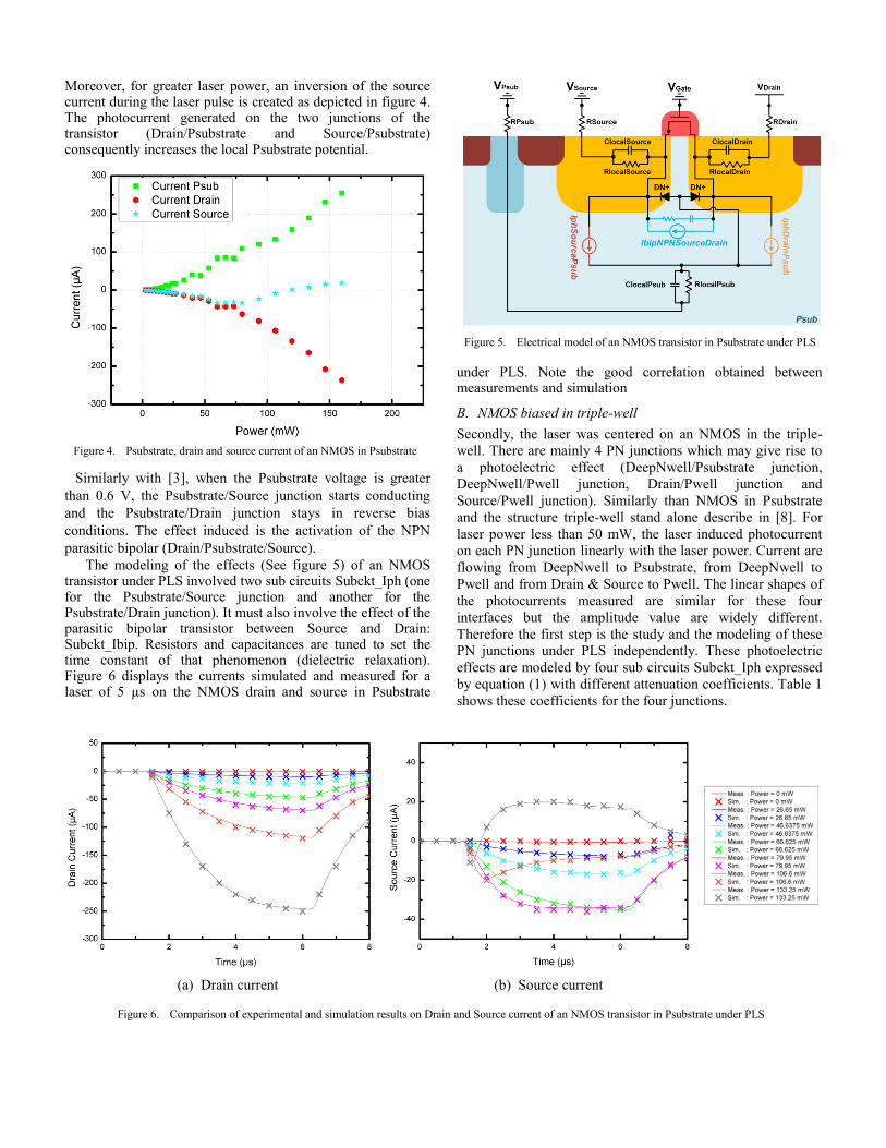
Moreover, for greater laser power, an inversion of the source current during the laser pulse is created as depicted in figure 4. The photocurrent generated on the two junctions of the transistor (Drain/Psubstrate and Source/Psubstrate) consequently increases the local Psubstrate potential.
Similarly with [3], when the Psubstrate voltage is greater than 0.6 V, the Psubstrate/Source junction starts conducting and the Psubstrate/Drain junction stays in reverse bias conditions. The effect induced is the activation of the NPN parasitic bipolar (Drain/Psubstrate/Source).
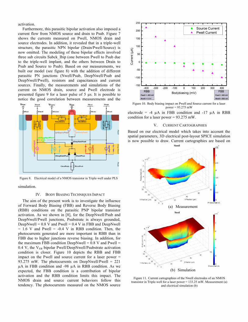
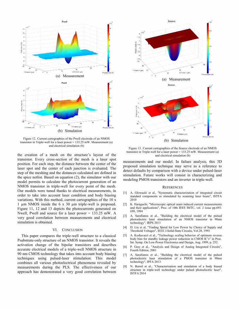
The modeling of the effects (See figure 5) of an NMOS transistor under PLS involved two sub circuits Subckt_Iph (one for the Psubstrate/Source junction and another for the Psubstrate/Drain junction). It must also involve the effect of the parasitic bipolar transistor between Source and Drain: Subckt_Ibip. Resistors and capacitances are tuned to set the time constant of that phenomenon (dielectric relaxation). Figure 6 displays the currents simulated and measured for a laser of 5 µs on the NMOS drain and source in Psubstrate
under PLS. Note the good correlation obtained between measurements and simulation
B. NMOS biased in triple-well Secondly, the laser was centered on an NMOS in the triple-well. There are mainly 4 PN junctions which may give rise to a photoelectric effect (DeepNwell/Psubstrate junction, DeepNwell/Pwell junction, Drain/Pwell junction and Source/Pwell junction). Similarly than NMOS in Psubstrate and the structure triple-well stand alone describe in [8]. For laser power less than 50 mW, the laser induced photocurrent on each PN junction linearly with the laser power. Current are flowing from DeepNwell to Psubstrate, from DeepNwell to Pwell and from Drain & Source to Pwell. The linear shapes of the photocurrents measured are similar for these four interfaces but the amplitude value are widely different. Therefore the first step is the study and the modeling of these PN junctions under PLS independently. These photoelectric effects are modeled by four sub circuits Subckt_Iph expressed by equation (1) with different attenuation coefficients. Table 1 shows these coefficients for the four junctions.
Figure 4. Psubstrate, drain and source current of an NMOS in Psubstrate
(a) Drain current (b) Source current
Figure 6. Comparison of experimental and simulation results on Drain and Source current of an NMOS transistor in Psubstrate under PLS
Figure 5. Electrical model of an NMOS transistor in Psubstrate under PLS

Moreover, when the NMOS, Pwell, DeepNwell and Psub are biased in a triple-well structure, for a laser power greater than 50 mW, an inversion of the Pwell, drain and source currents during the laser pulse are observed as depicted in figure 7. The Pwell and Psub potentials increase locally and the local Nwell potential decreases due to the parasitic well and access resistors. This is caused by the photocurrents generated on all the P/N junctions. These photocurrents induced a differential local voltage greater than 0.6 V between Pwell and DeepNwell. Then it caused the current to flow from Pwell to Psubstrate by the parasitic PNP bipolar transistor
(a) Drain current (b) Source current
(c) Pwell current
Figure 9. Comparison of experimental and simulation results on Drain, Source and Pwell current of an NMOS transistor in triple-well under PLS
TABLE I. ATTENUATION COEFFICIENTS MEASURED ON PHOTOELECTRIC AMPLITUDE FOR ALL PN JUNCTIONS
Junction Attenuation coefficient (γ) DeepNwell/Psubstrate 1 DeepNwell/Pwell 50 Drain/Pwell 500 Source/pwell 500
Figure 7. Pwell, drain and source current of an NMOS in triple-well
activation. Furthermore, this parasitic bipolar activation also imposed a
current flow from NMOS source and drain to Psub. Figure 7 shows the currents measured on Pwell, NMOS drain and source electrodes. In addition, it revealed that in a triple-well structure, the parasitic NPN bipolar (Drain/Pwell/Source) is now omitted. The modeling of these bipolar effects involved three sub circuits Subck_Ibip (one between Pwell to Psub due to the triple-well implant, and the others between Drain to Psub and Source to Psub). Based on our measurements, we built our model (see figure 8) with the addition of different parasitic PN junctions (Nwell/Psub, DeepNwell/Psub and DeepNwell/Pwell), resistors and capacitances and current sources. Finally, the measurements and simulations of the current on NMOS drain, source and Pwell electrode is presented figure 9 for a laser pulse of 5 µs. It is possible to notice the good correlation between measurements and the
simulation.
IV. BODY BIASING TECHNIQUES IMPACT The aim of the present work is to investigate the influence
of Forward Body Biasing (FBB) and Reverse Body Biasing (RBB) conditions on the parasitic PNP bipolar transistor activation. As we shown in [8], for the DeepNwell/Psub and DeepNwell/Pwell junctions, Psubstrate is always grounded, DeepNwell = 0.8 V and Pwell = 0.4 V in FBB and DeepNwell = 1.6 V and Pwell = -0.4 V in RBB condition. Then, the photocurrents generated are more important in RBB than in FBB due to higher junctions reverse biasing. In addition, for the maximum FBB condition DeepNwell = 0.8 V and Pwell = 0.4 V, the VEB bipolar Pwell/DeepNwell/Psubstrate activation condition is closer. Figure 10 depicts the RBB and FBB impact on the Pwell and source current for a laser power = 93.275 mW. The photocurrents on DeepNwell/Pwell = 221 µA in FBB condition and -98 µA in RBB condition. As we expected, the FBB condition is a contribution of bipolar activation and the RBB condition limits this impact. The NMOS drain and source current behaviors follow this tendency. The photocurrents measured on the NMOS source
electrode = -4 µA in FBB condition and -17 µA in RBB condition for a laser power = 93.275 mW.
V. CURRENT CARTOGRAPHIES Based on our electrical model which takes into account the spatial parameters, 3D electrical post-layout SPICE simulation is now possible to draw. Current cartographies are based on
Figure 8. Electrical model of a NMOS transistor in Triple-well under PLS
Figure 10. Body biasing impact on Pwell and Source current for a laser
power = 93.275 mW
(a) Measurement
(b) Simulation
Figure 11. Current cartographies of the Nwell electrodes of an NMOS transistor in Triple-well for a laser power = 133.25 mW. Measurement (a)
and electrical simulation (b)
the creation of a mesh on the structure’s layout of the transistor. Every cross-section of the mesh is a laser spot position. For each step, the distance between the center of the laser spot and the center of each junction is evaluated. The step of the meshing and the distances calculated are defined in the spice netlist. Based on equation (2), the simulator with our model permits to calculate the photocurrent generation of an NMOS transistor in triple-well for every point of the mesh. Our models were tuned thanks to electrical measurements, in order to take into account laser condition and body biasing variations. With this method, current cartographies of the 10 x 1 µm NMOS inside the 6 x 30 µm triple-well is proposed. Figure 11, 12 and 13 depicts the photocurrents generated on Nwell, Pwell and source for a laser power = 133.25 mW. A very good correlation between measurements and electrical simulation is obtained.
VI. CONCLUSION This paper compares the triple-well structure to a classical
Psubstrate-only structure of an NMOS transistor. It reveals the activation change of the bipolar transistors and describes accurate electrical models of a triple-well NMOS structure in 90 nm CMOS technology that takes into account body biasing techniques using pulsed-laser stimulation. This model combines all various photoelectrical phenomena revealed by measurements during the PLS. The effectiveness of our approach has demonstrated a very good correlation between
measurements and our model. In failure analysis, this 3D proposed simulation technique may serve as a reference to detect defaults by comparison with a device under pulsed-laser stimulation. Future works will consist in characterizing and modeling PMOS transistors and an inverter in triple-well.
REFERENCES [1] A. Glowacki et al., "Systematic characterization of integrated circuit
standard components as stimulated by scanning laser beam", ISTFA 2010
[2] K. Haraguchi, "Microscopic optical seam induced current measurements and their applications", Proc. of 10th IEEE IMTC, vol. 2 issue pp.693-699, 1994
[3] A. Sarafianos et al., "Building the electrical model of the pulsed photoelectric laser stimulation of an NMOS transistor in 90nm technology", IRPS 2013
[4] D. Liu et al, "Trading Speed for Low Power by Choice of Supply and Threshold Voltages", IEEE J.Solid-State Circuits, Vol.28, 1993
[5] A. Keshavarzi et al., "Technology scaling behavior of optimum reverse body bias for standby leakage power reduction in CMOS IC’s" in Proc. Int. Symp. On Low-Power Electronics and Design, Aug. 1999, p. 252.
[6] P. Gray et al., "Analysis and Design of Analog Integrated Circuits", Fourth Edition, 2001
[7] A. Sarafianos et al., "Building the electrical model of the pulsed photoelectric laser stimulation of a PMOS transistor in 90nm technology", IPFA 2013
[8] N. Borrel et al., "Characterization and simulation of a body biased structure in triple-well technology under pulsed photoelectric laser", ISTFA 2014
(a) Measurement
(b) Simulation
Figure 12. Current cartographies of the Pwell electrode of an NMOS transistor in Triple-well for a laser power = 133.25 mW. Measurement (a)
and electrical simulation (b)
(a) Measurement
(b) Simulation
Figure 13. Current cartographies of the Source electrode of an NMOS transistor in Triple-well for a laser power = 133.25 mW. Measurement (a)
and electrical simulation (b)