electrical spin injection and spin transport in semiconducting si … · electrical spin injection...
TRANSCRIPT
Electrical Spin injection and Spin transport in semiconducting Si and Ge channels
Joao Filipe Pires Cunha
[email protected] Superior Tecnico, Lisbon, Portugal
Under supervision of S. Freitas (INESC-MN/IST) and J.-M. George (UMP CNRS/Thales)(Dated: September 2014)
This work presents the development of some key steps for the fabrication of a Lateral Spin-Valve (LSV)structure for Non-Local (NL) spin injection/detection in Silicon. In order to overcome the impedance mismatchproblem a tunnel barrier solution in a stacking Co40Fe40B20/MgO/Si(n+) was adopted. A methodology tocharacterize the tunnel interface resistance was implemented and tested. As a result, for tMgO = 1 nm spininjection/detection in a LSV would be possible in the framework of the Fert-Jaffres model. Additionally, amethod for nanoscale definition of heavily doped Si channels in undoped Si by means of ion implantation wasdeveloped, opening the way for the fabrication of LSV structures in Si.
I. INTRODUCTION
The spintronics field is one of the youngestand most successful branches of condensed matterphysics, having provided already practical imple-mentations in magnetic field sensors or in memoryapplications such as hard-drive read heads and Mag-netic Random Access Memories (MRAM) [1]. Us-ing semiconductor spintronics, in the future, onecan imagine the fabrication of circuits that will al-low memory operations (as in MRAM) and logiccomputing (as in CMOS) at once. This integrationwill bring higher communication processing rate andlower power consumption when compared to the con-ventional electronics of today [2].
The first leap into the development of semiconduc-tor spintronics was in 1990, when special attentionwas given to the proposal of Datta and Das for aspin transistor [3]. In all the semiconductor candi-dates for spintronics, Si is today being considered asthe most promising one [4]. Injection of spin polar-ized electrons from a ferromagnetic electrode into aSi (non-magnetic) channel is one of the challenges tobuild Si based spin devices, such as the Si spin FieldEffect Transistor (FET). In fact, to make this kindof device real, not only good mastering of spin in-jection but also of spin propagation, manipulationand detection is required. However, to efficientlyinject spin into Si by electrical means, one has toovercome the impedance mismatch problem pointedout by Schmidt et al. [5] in a situation where wehave a simple system of a ferromagnetic material (F)and a semiconductor as non-magnetic material (N)in ohmic contact with an electrical current passingby. In fact when taking semiconductors in this F/Nsituation, because of their low (spin-dependent) den-sity of states compared to the F material, the spin-dependent resistances (defined as r = ρ · lsf , ρ be-ing the resistivity and lsf the spin diffusion length)verify rF rN which leads to a zero current spin
polarization in the N material.
One way to overcome the impedance mismatchproblem is to insert a finite spin-conservative inter-face resistance r∗b , like a tunnel barrier, at the in-terface [6]. There are other ways to achieve spin-polarized current injection such as using polarizedlight [7], hot electrons spin injection [8], Seebeck spintunneling [9], and dynamical spin pumping [10]. Theuse of a spin-conservative interface resistance to in-ject and detect spin-polarization in Si has been rec-ognized as the most viable and robust method sofar [11]. The concept behind this method is that,if the inserted interface resistance r∗b is sufficientlyhigh, the polarization of the injected current will bedetermined by the spin asymmetry of the interfaceresistance γ = (r+
b −r−b )/(r+
b +r−b ). This means thatthe transport across the interface barrier will be de-termined by the (spin-dependent) density of statesof the two electrodes involved in the process, suchthat if the current across the barrier is small, theelectrodes remain in equilibrium and so the relative(spin-dependent) resistances of the electrodes playno substantial role in defining or limiting the spin-dependent transport across the interface [2].
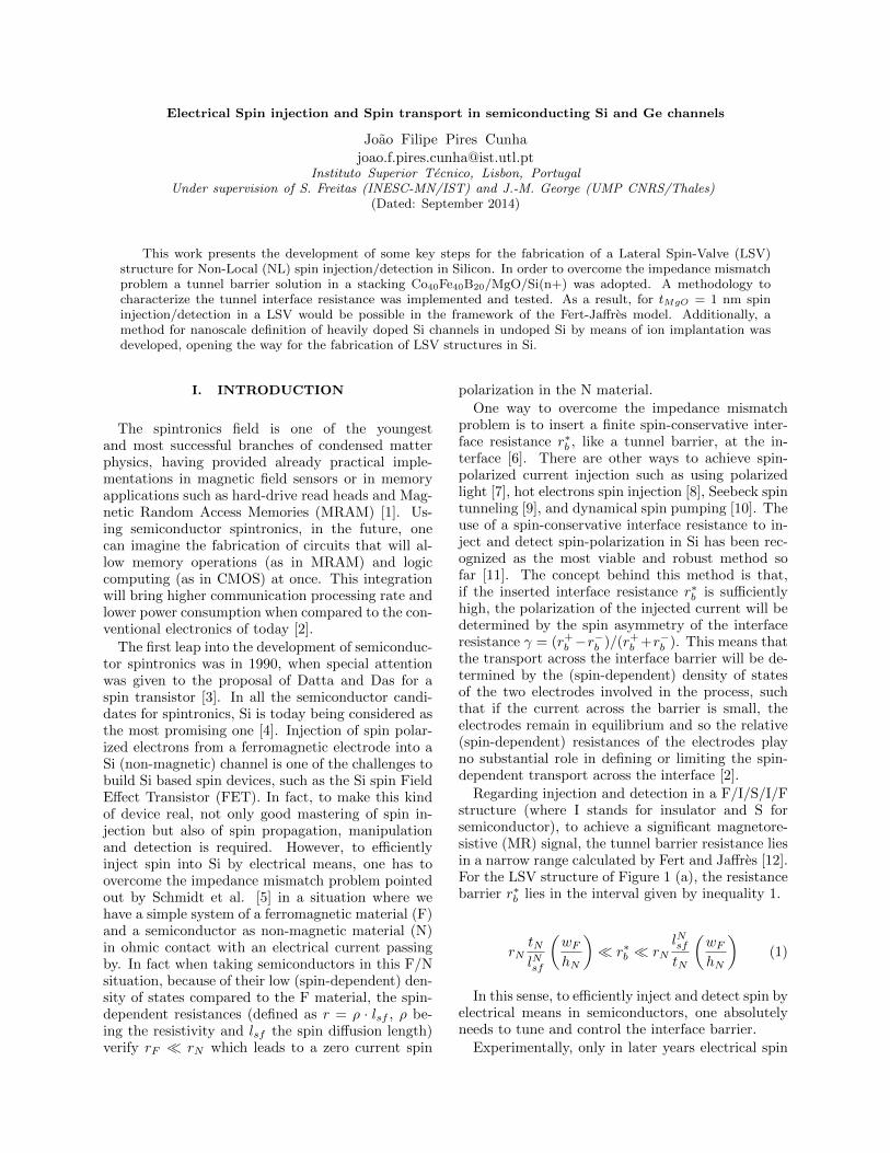
Regarding injection and detection in a F/I/S/I/Fstructure (where I stands for insulator and S forsemiconductor), to achieve a significant magnetore-sistive (MR) signal, the tunnel barrier resistance liesin a narrow range calculated by Fert and Jaffres [12].For the LSV structure of Figure 1 (a), the resistancebarrier r∗b lies in the interval given by inequality 1.
rNtNlNsf
(wFhN
) r∗b rN
lNsftN
(wFhN
)(1)
In this sense, to efficiently inject and detect spin byelectrical means in semiconductors, one absolutelyneeds to tune and control the interface barrier.
Experimentally, only in later years electrical spin
2
injection and detection into Si has been confirmedby overcoming the impedance mismatch with tunnelbarriers as Al2O3 by Dash et al. [13], MgO by Jonkeret al. [14], Fe3Si Schottky barrier or even grapheneVan’t Erve et al. [15]. In 2007, Appelbaum et al. [8]reported the first spin electrical injection, transportand detection in undoped Si at low temperature, us-ing hot electrons. Right after in same year Jonker etal. [14] reported electrical spin injection into Si fromFe electrodes with an Al2O3 tunnel barrier at lowtemperature, using an optical detector and circularlypolarized luminescence of a Si-based LED. Later inthat year, Van’t Erve et al. [16] reported spin electri-cal injection, transport and detection at 10 K, usinga ferromagnetic tunnel barrier. The jump from lowtemperature spin injection to room temperature spininjection was made in 2009 by Dash et al. [13] us-ing a Ni80Fe20/Al2O3 tunnel barrier and both highdoped n-Si and p-Si. The shift to heavily doped Siwas followed by many groups, such as Jeon et al. [17]with MgO tunnel barrier and Suzuki et al. [18] thatdemonstrated the first non-local detection of spin ac-cumulation in Si at room temperature. Recently Jainet al. [19] showed efficient spin injection in the con-duction band of n-Ge at room temperature using aMgO tunnel barrier.
Most of the referred experiments were performedusing a Three-terminal spin injection/detection ge-ometry and Hanle effect [20]. In fact, the Three-terminal injection/detection geometry [21] is nowa-days the classical (and the most widely used) way todetect spin injection into semiconductors (S). How-ever the spin accumulation signal found using thisThree-terminal geometry shows disagreement withFert-Jaffres theory by several orders of magnitude[13]. Tran et al. [22] suggested that this can be ex-plained when considering two-step tunneling acrossinterface states in the interface F/S. More recentlyHolly et al. [23] show that in Three-terminal devicesthe MR signal is being erroneously interpreted sinceit is due to inelastic scattering in the interface andnot to bulk spin transport and spin accumulation inthe semiconductor.
On the other hand, the measurement of a Non-Local (NL) voltage in a Lateral Spin Valve (LSV)structure is the undoubtable and most reliable wayto demonstrate spin injection, accumulation andtransport inside the semiconductor channel. In thisgeometry, the voltage measurement circuit is phys-ically separated from the current circuit as shownin Figure 1 (b), and there is no voltage noise fromthe injector and the N channel at the detector site,giving high sensitivity in spin detection.
Therefore, this work presents some keys stepstowards the realization of NL measurementsin Si by (i) the implementation of a tun-
Figure 1: (a) Lateral Spin Valve in a closed channelgeometry considered in this work, showing
definition of geometrical parameters that will beused. Adapted from [12]. (b) Non-Local
measurement scheme: a current is imposed in theferromagnetic injector and a voltage, directly
related to the spin accumulation at the detectorsite, is measured in the ferromagnetic detector. In
this geometry, there is a physical separation ofcharge and spin current. Adapted from [24].
nel barrier resistance characterization method inCo40Fe40B20/MgO/Si(n+) in order to find the opti-mal injection/detection condition in the frameworkof the Fert-Jaffres model [12] and by (ii) providing amethod for the definition of nanoscale highly dopedchannels in undoped Si using a step of ebeam lithog-raphy and ion implantation. The advantage of thismethod is to make it possible to fabricate LSV planestructures with a very thin tunnel barrier, avoidingtop-down fabrication issues.
II. RESULTS
A. Characterization of the interface resistance
To characterize the tunnel barrier resistance,samples patterned with circular nanopillars de-fined via ebeam with projected radius going from25 nm until 505 nm were fabricated. The stack-ing was Au(30)/CoFeB(5)/MgO(var)/Si(n+)(215)all deposited via magnetron sputtering with datain nm and variable MgO thickness being tMgO =1, 1.7, 2.1, 3.1 nm. A sample without MgO ref-erenced as tMgO = 0 nm was also fabricated.The substrate is a Silicon-On-Insulator wafer withSi(n+)(215)/SiO2(200)/Si. The top layer referredto as Si(n+) is heavily doped at 2× 1019 cm−3.
The electrical measurements were performed us-ing the Conductive Tip Atomic Force Microscopy

3
(CTAFM) technique equipped with a voltage sourceand a nanoampmeter KEITHLEY model 2636A con-trolled by LABVIEW. The procedure is such thatby using tapping mode AFM, the AFM tip is placedover a nanopillar (see Figure 2) and, by switching tocontact mode AFM, the tip works as a top contact tothe pillar whose bottom is connected to the ground.Then a bias voltage Vbias is applied to the nanopillarand the current is measured. The I-V characteristicis in this way acquired when sweeping the appliedVbias in [−1, 1] V. The voltage ramp is applied threetimes to assure it is the characteristic I-V tunnelcurve that is being acquired. The procedure is re-peated for pillars with different cross-sectional areas,and by joining electrical and topographical informa-tion, the RA product, a characteristic measure of thetunnel junction for a certain tMgO, is computed.
Figure 2: CTAFM measurement scheme. Thenanopillars electrical characteristics were acquired
making use of the Keithley model, while otherCTAFM measurements of local resistance profile of
Si nanowires were acquired with the I/Vlogarithmic converter setup. We can choosebetween these two “modes of operation” by
controlling the position of the switch SW (the twoswitch positions are labeled A and B, and as can be
seen, the position of the switch SW controls theground or I/V connection of the sample’s back
side).
1. Study of I-V curves
To identify tunnel transport between two elec-trodes, the I-V curve should (following Rowell cri-teria [25] [26]) (i) have exponential behavior withtunnel barrier thickness, (ii) be well fitted by theo-retical models like Simmons’ [27] or Brinkman’s [25]and (iii) the tunnel resistance should increase slightlywhen going from room temperature to low tempera-ture.
To evaluate the tunneling behavior of the acquiredI-V curves one can use the Simmons model [27]. Forrelatively low voltages V < φeff/e, the I-V is ap-proximated by I = αV + βV 3 [27] [28] with
α = S(eh
)2 √2mφeff
deffexp
[−D
√φeff
]β = S
((De)2
96φeff− De2
32φ3/2eff
) (2)
where D = (4πdeff√
2m)/h, m is the electron mass,h the Planck’s constant, e the electron charge andS the cross-sectional area of the nanopillar. Per-forming the fit, presented in Figure 3, we obtain theresults of the Table I. We can see that the parame-ters are coherent since we obtain a barrier thicknesscompatible with the physical thickness [29] and fur-thermore the obtained barrier height is in agreementwith what can be found in the literature (around1 eV) in electrical characterization of magnetic tun-nel junctions [28] [30].
-1.0 -0.5 0.0 0.5 1.010-11
10-10
10-9
10-8
10-7
Vbias HVL
ÈIÈHAL
Figure 3: I-V curve fitting for tMgO = 2.1 nm, withI = αV + βV 3 as fitting expression. We can see theexperimental data in blue and fitting curve result in
red.
deff (nm) φeff (eV)2.36± 1.4 0.94± 0.52
Table I: Effective barrier thickness and heightextracted from I-V curve fitting of Figure 3.
2. Resistance window
For each tMgO we assign RA(Vbias). The Fert-Jaffres model is valid for small bias, where the flat-band approach is valid and therefore we are inter-ested in the value of RA
∣∣Vbias=0.2 V
as function of
tMgO that we can see in Figure 4.

4
Figure 4: Data RA∣∣Vbias=0.2 V
. We can clearly
identify two regions: (i) for thin MgO layers theSchottky transport process dominates and (ii) forthick MgO layers the tunnel transport dominates.The maxima of the MR curves for several typicallNsf following Fert-Jaffres with parameters β = 0.46
(the bulk spin asymmetry coefficient), γ = 0.5 (thespin asymmetry of the interface resistance),
ρF = 300 Ω · nm, ρN = 27700 Ω · nm, lFsf = 15 nm,hN = 215 nm and wN = 100 nm are represented in
the same plot.
In the Figure 4 we can observe that the tun-nel barrier resistance increases exponentially withthe thickness of the insulating layer for thickervalues of this parameter, which supports the as-sumption of dominant tunneling transport. SinceRAtun ∝ exp (2κdeff ) and considering the effectivemass m∗MgO = 0.46me from reference [31] we obtainby fit φeff = 1.02±0.02 eV, which is consistent withthe value obtained by the I-V curve fitting presentedbefore. Also, the RA product increases by several or-ders of magnitude when the thickness of the tunnelbarrier is increased. For thin insulating layers, theSchottky transport mechanism dominates, giving aresistance stagnation around 1 kΩ, the Schottky re-sistance.
The condition for efficient electrical spin injec-tion [12] can be calculated for the LSV structure.The MR depends on parameters of the materi-als such as the bulk spin asymmetry (defined asβ = (σF+ − σF−)/(σF+ + σF−)) of the CoFeB layerthat is not exactly known and was considered to beβ = 0.46 or the asymmetry of the interface resis-tance that was taken to be γ = 0.5. The resistivityof the materials is one of the fundamental param-eters. The resistivity of the semiconductor film isparticularly important, since it strongly depends onparameters such as temperature and doping concen-tration. By van der Pauw measurement the resistiv-ity of the top heavily doped Si layer was found to beρtop Si = 2.77 mΩ · cm at room temperature.
Figure 5: Experimental data of the tunnel barrierRA product for the Au/CoFeB/MgO/Si(n+)system at Vbias = 0.2 V together with MR
maximum values following Fert-Jaffres [12] with thesame parameters as in Figure 4.
Figure 6: MR window representation (withassigned parameters) as function of wF and rb for
lNsf = 5 µm.
The free parameters (not related to the materi-als) when computing the MR are the spin diffusionlength lNsf (unknown), the F electrode width wF , theN film thickness and the distance between the F elec-trodes tN . Fixing tN = 200 nm (smaller than thetypical lNsf [32]) and hN = 215 nm the only param-eter remaining free is wF . But, it is required thatwF lNsf to avoid loss of spin in the vicinity ofthe F electrodes, a condition we fulfill by consideringlNsf = 10wF . Taking all this into account, the MR
curve is represented together with the RA(tMgO)curve for three typical lNsf in Figure 5. Also, themaximum value of these MR curves is representedalso in Figure 4.
We can represent the data together with the re-sistance window, obtaining Figure 5 and varyingthe wF from 10 nm until lNsf we can represent
MR(wF , rb) as in the Figure 6, for lNsf = 5 µm. The

5
advantage of this representation is that one can seefor which wF does the resistance barrier enter intothe window.
Some conclusions can be taken:
• For lNsf between 1 and 10 µm we can compute
rN = ρN · lNsf of 10 to 102 Ω · µm. Representingit in Figure 6, it arrives just inside the resis-tance window;
• We enter in the MR window when tMgO =1 nm (or lower, if the MgO barrier is still con-tinuous, looking at Figure 4), obtaining 5% ofMR if lNsf = 5 µm and 17% if lNsf = 10 µm.
Si is known for having a large lNsf , however the lNsfrequired here place us on the limit of the largest val-ues found in the literature [32]. In this situation, onecan look at other variables of the system in order toenlarge the resistance interval of inequality 1 suchas the hN (semiconductor layer thickness), chang-ing it to 100 nm, ar the tN (distance between the Felectrodes), changing it to 150 nm, and at the dop-ing concentration (that will influence rN ). In theseconditions we get into the window achieving a fewpercent MR even when lNsf = 1 µm.
B. Definition of Si heavily doped channels
The semiconductor channel in the LSV structurewe consider here will be made of heavily doped Si,surrounded by undoped Si. Since the channel is verythin (in the order of hundreds of nm), we adopt thenomenclature of Si nanowires.
In this work, concerning the fabrication of thiskind of structure, a bottom-up approach was devel-oped. It consists in the definition of heavily dopedSi nanowires in undoped Si using a mask during Pion implantation. Then, to overcome the impedancemismatch problem, deposition of MgO with tMgO =1 nm on top of the plane Si surface takes place. Hav-ing a totally plane structure allows to avoid any con-tinuity problem in the MgO film that will arise if thechannel was already etched.
To test this new solution, Monte Carlo ion implan-tation simulations (1.) were performed. They wereperformed first in Si, to obtain critical implantationparameters such as the acceleration energy Eacc andimplantation dose Q required to obtain a doping con-centration of 1019 cm−3. Right after, the same kindof simulations were performed in Si with a protectingmask in order to know what is the required thick-ness for this mask to stop the implantation ions.The nanowires mask is defined using ebeam lithog-raphy. After implantation, the mask is removed andthe nanowires are subjected to an annealing step in
order to activate the implantation ions. On the elec-trical characterization (2.) of the nanowire samples,Hall measurements on reference samples were doneto know the doping level, mobility and resistivity,and CTAFM imaging on patterned samples were per-formed in order to study the resistivity profile of thethese samples.
1. Ion Implantation
Ion implantation is the most common techniqueto introduce dopant atoms into Si. In here, P ions(classical donor for obtaining a n-type semiconduc-tor) get accelerated under an electrostatic field, be-ing fired into Si.
For our purpose, since the top film of this SOIhas 100 nm of thickness and we want to achieve anuniform doping of this layer, the range (distance inwhich one ion loses all its energy by means of col-lisions inside the material to where it was shot) isset to be 50 nm. The SRIM code [33] provides anenergy loss calculation, i. e. a correspondence be-tween the ion Eacc and the range, that is plotted inFigure 7. By linear fit [34] we get Eacc
∣∣Rp=50 nm
=
35.46±0.05 keV and we can consider it to be 35.5 keVfor practical purposes.
SRIMFit
10 20 30 40 50 60 700
20
40
60
80
100
Eacc HkeVL
Pro
ject
edR
ange
Rp
HnmL
Figure 7: Linear fit Rp(nm) = a×E(keV) + b to theenergy loss simulation data calculated with SRIM.We obtain as parameters b = 3.97± 0.06 nm/keVand a = 1.30± 0.01 nm. Inverting the linear fit
formula we find Eacc∣∣Rp=50 nm
= 35.46± 0.05 keV.
Of particular relevance is the result that the con-centration of the implanted atoms in the target ma-terial as function of distance follows a gaussian pro-file. The TRIM code [33] produces implantation con-centration profiles that can be fitted to extract theprojected range Rp, the range straggling (standarddeviation) ∆Rp and the adimensional constant A.The concentration of implantation ions C depends

6
also on the time and temperature (implicitly throughD(T ) = D0 exp(−Eact/kBT )) of the annealing step.The full profile is given by Eq. 3 [34]
C(x, t)
Q=
A√π[2(∆Rp)2 + 4D(T )t]1/2
exp
(−
(x− Rp)2
2(∆Rp)2 + 4D(T )t
)(3)
Figure 8 was produced in the before annealing sit-uation where t = 0, giving the fit results referred inthe Figure’s caption.
TRIMFit
0 20 40 60 80 100
104
105
Depth HnmL
CHxL
QHIo
nscm
3L
HIons
cm2
L
Figure 8: Fit to TRIM results and gaussian fittingfollowing expression 3 with t = 0. One obtains
A = (1.019± 0.006)× 108, Rp = 51.3± 0.2 nm and∆Rp = 23.1± 0.2 nm.
Using Eq. 3, in Figure 9 (a) is computed Cas function of the implantation dose. For a tar-get concentration of 1019 ions/cm3 one needs Q =5.5× 10¹⁴ ions/cm2, when considering a thermal an-nealing of T = 900 oC and tannealing = 90 min. InFigure 9 (b), the evolution of the concentration pro-file is presented for various annealing temperatures.
Using TRIM with a stacking PMMA/Si it was ob-tained that 200 nm of PMMA are sufficient to stopthe implantation ions.
2. Characterization of Si heavily doped channels
CTAFM at room and low temperature.
To obtain a 2D local resistance map, a CTAFMtechnique was used where a doped diamond tip wasscanned in contact mode over the sample (same ex-perimental setup of the Figure 2, where one simplychanges the position of the switch SW). Since Si withdifferent doping levels will show different resistivities[29], a contrast in the local resistance values is ex-pected once that Rlocal ∝ ρ.
T=800ºCT=850ºCT=900ºCT=950ºCT=1000ºCT=1050ºC
1014 1015
1018
1019
Implantation Dose Hionscm2L
Con
cent
ratio
nHio
nscm
3L
Fixed tannealing=90 min. and Depth=50 nm
Figure 9: Concentration as function of implantationdose for annealing time t = 90 min and depthx = 50 mathrmnm, to obtain the target doping
concentration n = 1× 10¹⁹ ions/cm3 one canchoose Q = 5.5× 10¹⁴ions/cm2 as implantation
dose after annealing at T = 900 oC.
During experimental characterization several as-pects such as surface oxidation of the Si, space chargeeffects, Si metallic phase transitions and mechanicalsample degradation during imaging had to be care-fully addressed. Solving step by step these difficul-ties, it was possible to conclude that for a satisfactoryimaging, such as the one in Figure 10:
• Previous HF treatment (that was optimized to30 s for HF diluted at 2%) was needed;
• One should avoid high mechanical pressuressince they lead to sample degradation and Siphase transitions.
Finally from CTAFM characterization it can beconcluded that when looking at left part of Figures10 (a) and (b) the implanted region shows no topo-graphic contrast with respect to the undoped matrix.Further we observe one order of magnitude of resis-tance contrast at room temperature (right part ofFigure 10 (a), measurements at Figure 10 (c)) thatgets enhanced to two orders of magnitude at 77 K(right part of Figure 10 (b), measurements at Figure10 (d)).
Hall measurements.
Unmasked reference samples consisting in bareSOI (where we are interested in the top Si layer,not protected with PMMA) and SOI protected withPMMA were also subjected to the ion implantationprocess. The results are presented on Table II.

7
Figure 10: CTAFM images at 300 K for (a), (c), (e) and 77 K for (b), (d), (f); (a) and (b), topographicimage and CTAFM image, the heavily doped nanowire is not visible in the topographic image, and it isclearly visible in the resistance map; (c) and (d) resistance profile cut: at room temperature one finds
roughly one order of magnitude that gets enhanced at 77 K; (e) and (f) 3D local resistance map.
Sample Si not Si protectedprotected with PMMA
n (cm−3) at 300 K 3.32 × 10¹⁹ 1.46 × 10¹⁷
n (cm−3) at 90 K 3.24 × 10¹⁹ 1.99 × 10¹⁶
ρ (mΩ · cm) at 300 K 2.5 92.7ρ (mΩ · cm) at 90 K 1.4 411.8
Table II: Results of the Hall measurements at roomand low temperature.
The Hall measurement data is coherent with theCTAFM imaging, both techniques showing similarresistivity ratios between Si not protected and pro-tected with PMMA . We extract from the Hall mea-surements a doping concentration 1019 cm−3 in theheavily doped nanowire and 1017 cm−3 at room tem-perature and 1016 cm−3 at low temperature in thesample protected with PMMA.
The protected zone conducts better than raw Si
(data not shown here), which is unexpected. Thisis explained by considering that the PMMA is nota powerful mask against P ion bombardment, andor the mask thickness was insufficient to stop them(contradicting the results of the simulation), or someother phenomena referred in literature [35] such asdecomposition of the PMMA took place during bom-bardment.
Test of SiO2 as masking material.
To enhance the resistivity contrast, other maskingmaterial (SiO2) was tested. For this material, TRIMsimulations showed that 150 nm is the minimum pro-tecting thickness.
To test the efficiency of SiO2 as a mask duringimplantation, samples were coated with 200 and250 nm of PMMA plus 150 and 200 nm of SiO2.

8
They were subjected to ion implantation togetherwith a bare Si sample. Then Hall measurements werecarried out on them.
After ion implantation, the color of the substratechanged for the unprotected and PMMA protectedsamples. The resulting doping concentration ex-tracted from Hall measurements are reported in Fig-ure 11 as function of the masking material thickness(PMMA and SiO2). These results clearly shows thatPMMA does not fully protect the Si from the implan-tation contrarily to SiO2. As a conclusion, the SiO2
mask will be required for the future.
Si impRaw SiSi PMMASi SiO2
0 50 100 150 200 250 3001015
1016
1017
1018
1019
1020
Protecting layer thickness HnmL
Dop
ing
conc
entr
atio
nHcm
-3
L
Figure 11: Doping concentration measured by Hallmeasurement technique as function of the
protecting mask thickness. The error bars are dueto dispersion in consecutive measurements.
III. CONCLUSION
This work develops some fundamental milestonesinto the realization of a LSV for NL measurementsin Si.
On the first part, a versatile and fast experimen-tal method for the characterization of the tunnelbarrier resistance was implemented, providing a fullcharacterization of the Co40Fe40B20/MgO/Si sys-tem. The experimental data were analyzed underthe Fert-Jaffres model and in general the requiredtunnel resistance is in the upper limit of the win-dow required for efficient spin injection/detection.For tMgO = 1 nm, lNsf = 5 µm and wF = 500 nm
(or higher but never crossing the lNsf limit, as it was
determined in Figure 6) it should be possible to ad-just the interfacial resistance in the resistance win-
dow of the Fert-Jaffres model. Moreover, a work[36] has recently been published reporting fabrica-tion and measurement at 300 K of a NL structureusing a Fe/MgO tunnel barrier in Si. In there, theyused a large voltage bias (out of the validity rangeof the Fert-Jaffres model) and a thicker MgO barrier(tMgO = 1.6 nm) obtaining however a generous NLsignal. This shows there are possibly another waysto change the resistance window in an advantageousway when considering drift-diffusion.
More generally, the possibility to characterize theinterface resistance on a large resistance range, asdeveloped in this thesis, is a particularly interestingtool which was successfully applied to other struc-tures such as Ge. In this case, it was possible toobtain RA(tMgO) curves similar to the one of theFigure 4, being observed a clear tunneling behaviorfor tMgO > 1 nm. These results can be used to ex-plain the recent demonstration of spin injection inthe conduction band of Ge by spin pumping [37],when a tunnel barrier is present between the semi-conductor and the ferromagnetic material.
A second part of the work was dedicated to thefabrication of Si heavily doped nanowires by ion im-plantation. The advantage of this technique is toprovide the possibility of fabrication of NL structuresby lift-off techniques compatible with the depositionof very thin insulating barriers. Here, it was shownthat the PMMA does not act as a powerful mask forimplantation. However, it still leads to a resistiv-ity contrast ratio of one order of magnitude at 300K(enhanced by one order of magnitude when goingto 77 K) between implanted zone and masked zone,revealing the potential of this approach. For the fu-ture, it was shown that the use of 200 nm of SiO2 asa mask appears to be a more efficient solution.
In a more general way, this channel definitionmethod for LSV fabrication can be used with othermaterials than ferromagnetic ones. For instance, theproposed method could also be invaluable to test newmechanisms of spin injection using large Spin HallAngle materials (where spin injection takes place viaSpin Hall Effect) like Pt, Au(W) or W [38]. In thiscase, we just need to replace the MgO/ferromagneticspin injector by the large Spin Hall Angle material.
IV. ACKNOWLEDGEMENTS
This master thesis project is the result of my in-ternship in the UMP CNRS/Thales at Thales Re-search and Technology in Palaiseau, Paris, Franceenglobed in the project SiGeSPIN. I acknowledge allthe team that welcomed me during this period oftime, in particular J.-M. George and P. Laczkowski.
9
[1] C. Chappert, A. Fert, and F. N. Van Dau, Naturematerials 6, 813 (2007).
[2] S. Wolf, D. Awschalom, R. Buhrman, J. Daughton,S. Von Molnar, M. Roukes, A. Y. Chtchelkanova,and D. Treger, Science 294, 1488 (2001).
[3] S. Datta and B. Das, Applied Physics Letters 56,665 (1990).
[4] R. Jansen, Nature Materials 11, 400 (2012).[5] G. Schmidt, D. Ferrand, L. Molenkamp, A. Filip,
and B. Van Wees, Physical Review B 62, R4790(2000).
[6] E. Rashba, Physical Review B 62, R16267 (2000).[7] G. Lampel, Physical Review Letters 20, 491 (1968).[8] I. Appelbaum, B. Huang, and D. J. Monsma, Na-
ture 447, 295 (2007).[9] J.-C. Le Breton, S. Sharma, H. Saito, S. Yuasa, and
R. Jansen, Nature 475, 82 (2011).[10] E. Shikoh, K. Ando, K. Kubo, E. Saitoh, T. Shinjo,
and M. Shiraishi, Physical Review Letters 110,127201 (2013).
[11] A. Dankert, R. S. Dulal, and S. P. Dash, Scientificreports 3 (2013).
[12] A. Fert and H. Jaffres, Physical Review B 64, 184420(2001).
[13] S. P. Dash, S. Sharma, R. S. Patel, M. P. de Jong,and R. Jansen, Nature 462, 491 (2009).
[14] B. T. Jonker, G. Kioseoglou, A. T. Hanbicki, C. H.Li, and P. E. Thompson, Nature Physics 3, 542(2007).
[15] O. Van’t Erve, A. Friedman, E. Cobas, C. Li,J. Robinson, and B. Jonker, Nature Nanotechnol-ogy 7, 737 (2012).
[16] O. van t Erve, A. Hanbicki, M. Holub, C. Li, C. Awo-Affouda, P. Thompson, and B. Jonker, AppliedPhysics Letters 91, 212109 (2007).
[17] K.-R. Jeon, B.-C. Min, I.-J. Shin, C.-Y. Park, H.-S. Lee, Y.-H. Jo, and S.-C. Shin, Applied PhysicsLetters 98, 262102 (2011).
[18] T. Suzuki, T. Sasaki, T. Oikawa, M. Shiraishi,Y. Suzuki, and K. Noguchi, Applied physics express4, 023003 (2011).
[19] A. Jain, J.-C. Rojas-Sanchez, M. Cubukcu, J. Peiro,J. Le Breton, E. Prestat, C. Vergnaud, L. Louahadj,C. Portemont, C. Ducruet, et al., Physical ReviewLetters 109, 106603 (2012).
[20] E. Y. Tsymbal and I. Zutic, Handbook of spin trans-port and magnetism (CRC press, 2011).
[21] I. Zutic, J. Fabian, and S. D. Sarma, Reviews ofmodern physics 76, 323 (2004).
[22] M. Tran, H. Jaffres, C. Deranlot, J.-M. George,A. Fert, A. Miard, and A. Lemaıtre, Physical re-view letters 102, 036601 (2009).
[23] P. L. Holly N. Tinkey and I. Appelbaum, APL 104(2014).
[24] R. Jansen, S. P. Dash, S. Sharma, and B. Min,Semiconductor Science and Technology 27, 083001(2012).
[25] W. Brinkman, R. Dynes, and J. Rowell, Journal ofApplied Physics 41, 1915 (1970).
[26] E. Burstein and S. Lundqvist, Tunneling phenomenain solids (Springer, 1969).
[27] J. G. Simmons, Journal of Applied Physics 34(1963).
[28] T. Kiyomura, Y. Maruo, and M. Gomi, Journal ofApplied Physics 88, 4768 (2000).
[29] S. M. Sze and K. K. Ng, Physics of SemiconductorDevices (Wiley, 2007).
[30] F. Magnus, S. Clowes, A. Gilbertson, W. Branford,E. Barkhoudarov, L. Cohen, L. Singh, Z. Barber,M. Blamire, P. Buckle, et al., Applied Physics Let-ters 91, 122106 (2007).
[31] A. Facchetti and T. J. Marks, From Synthesis toApplications, Wiley, Chichester, UK , 17 (2010).
[32] T. Sasaki, T. Oikawa, T. Suzuki, M. Shiraishi,Y. Suzuki, and K. Tagami, Applied Physics Express2, 053003 (2009).
[33] J. F. Ziegler, J. P. Biersack, and M. D. Ziegler,SRIM, the stopping and range of ions in matter(Lulu. com, 2008).
[34] S. Selberherr, Analysis and simulation of semicon-ductor devices (Springer Wien; New York, 1984).
[35] J. F. Ziegler, Ion Implantation Science and Technol-ogy 2e (Elsevier, 1988).
[36] T. Sasaki, T. Suzuki, Y. Ando, H. Koike, T. Oikawa,Y. Suzuki, and M. Shiraishi, Applied Physics Let-ters 104, 052404 (2014).
[37] J.-C. Rojas-Sanchez, M. Cubukcu, A. Jain,C. Vergnaud, C. Portemont, C. Ducruet, A. Barski,A. Marty, L. Vila, J.-P. Attane, et al., Physical Re-view B 88, 064403 (2013).
[38] P. Laczkowski, J.-C. Rojas-Sanchez, W. Savero-Torres, H. Jaffres, N. Reyren, C. Deranlot, L. Notin,C. Beigne, A. Marty, J.-P. Attane, et al., AppliedPhysics Letters 104, 142403 (2014).