electron beam lithography - rowan...
TRANSCRIPT

Electron Beam Lithography With the LEO Electron Microscope and Nanometer Pattern Generation System (NPGS)
Version 1.2
Revision History
Version 1.0 by Tim Osedach (email: [email protected]) - 12.21.2004 Version 1.2 by Tim Osedach (email: [email protected]) - 02.10.2005

Table of Contents 1. Introduction …………………1 2. Pattern Design
2.1 Design Considerations …………………1 2.1 DesignCAD LT …………………1
3. Generating a Run-File …………………4 4. e-beam Resists
4.1 Poly(methyl methacrylate) (PMMA) …………………8 4.2 Hydrogen silsesquioxane (HSQ) …………………8
5. Processing a Run File
5.1 Sample Mounting and Preparing the Microscope …………………8 5.2 Measuring the Beam Current …………………14 5.3 Collecting Focus Points …………………15 5.4 Executing your Run File …………………16
6. Conclusion …………………18

1. Introduction This tutorial is intended to provide you with a basic understanding and ability to write nanoscale patterns with electron beam lithography using Rowan’s LEO Scanning Electron Microscope. Pattern design using DesignCAD LT, the generation of NPGS Run-Files, coating of samples with e-beam resists, and the writing of those patterns with the SEM will be discussed. Before reading this tutorial you should have reached an intermediate level of skill using the SEM. If you don’t feel totally comfortable using the microscope, see the SEM manual written by Dan Marks. As the material presented within only covers the absolute basics of the enormously complicated procedure of electron beam lithography, you may want to also have the official NPGS manual available to go into more detail on subjects that may not be explained so thoroughly. This tutorial is in no way a substitute for training by somebody experienced with e-beam lithography, but should serve as a useful guide until you get on your feet. 2. Pattern Design 2.1 Design Considerations The first step towards writing a pattern using the electron microscope is designing the pattern to be written and translating it into a CAD file that can be recognized by the Nanometer Pattern Generation System (NPGS) software. Several factors must be taken into consideration at this early stage in the process:
Whether you are using a positive e-beam resist (areas exposed by the electron beam are removed during developing) or a negative e-beam resist (areas not exposed by the electron beam are removed during developing) will have a major impact on how you design your pattern.
The time required to write the pattern may be an issue. For example, the time needed to write a pattern can reach several hours for patterns that possess large features (several mm2).
The electron beam can affect regions as far as 5µm from large exposures. This can sometimes result in unintended regions being exposed and subsequently developed away (proximity effects).
Special attention must be taken during pattern design when e-beam writing without a beam blanker. Because the beam cannot be blanked as it moves between patterns to be written, streak-like exposures may be observed. With clever layout of your design and some care, the occurrence of these anomalies can be minimized.
Your ability to fully exercise these design considerations will likely come only through experimentation and acquiring experience. 2.2 DesignCAD LT Once you have a good idea of what you want your pattern to look like the next step is to draw that pattern into DesignCAD LT. When you open NPGS, a window like the one shown in Figure 1 will come up.

Figure 1. Nanometer Pattern Generation System Window.
Click on DesignCAD LT button to open the CAD software. It functions very similarly to normal CAD programs such as AutoCAD, with a few important exceptions. Though the units are given in inches, they are taken by NPGS to represent micrometers. Also, there are several NPGS-specific functions available. The distinction between NPGS functions and DesignCAD tools is an important one, because NPGS will not recognize patterns drawn with all of the DesignCAD tools. For example, lines and text written using DesignCAD tools must be converted to patterns recognizable to NPGS using the “To Vector” function. Generally, once you are done drawing your pattern you will need to run this function by clicking the “TV” button on the NPGS toolbar. It will automatically detect any features that need to undergo this conversion. To draw a filled polygon, you need to use the NPGS “Polygon Filled” function. You can select this tool by clicking on the “PF” button in the NPGS toolbar or by clicking the NPGS tab and selecting “Polygon Filled.” Instructions for using NPGS tools will appear in the lower left of the window once you select them. A pattern drawn using this tool is shown in Figure 2.

Figure 2. NPGS Info Box.
Different shapes within a pattern can be assigned to different layers by clicking on that shape and then on the “information” button. Additionally, shapes of the same layer can be distinguished by assigning them different colors. These options become extremely useful when it is required that different objects within be pattern be written very differently (different doses or exposure settings for example). Thus, layers and colors become a major consideration later on when creating a run file to specify how your pattern is to be written. Another important function is “Change Sweep.” Selecting a filled polygon and running this function will indicate the edge from which the electron beam will begin sweeping. The circle drawn on the lower side of the trapezoid shown in Figure 3 indicates that the beam will begin writing at that edge and that it will fill the rest of the pattern by sweeping parallel to that edge.

Figure 3. NPGS ChangeSweep function.
You are then given the option to change the sweep side by hitting ‘y’ or ‘n’. If you do wish to change the sweep side, you will be prompted to click on the two points describing the edge you wish to change the sweep side to. Setting the sweep sides intelligently can prevent the streaking mentioned earlier from ruining important parts of your pattern. An important pitfall to beware of is that saving and opening of files from within DesignCAD must be done using the NPGS functions and NOT by using DesignCAD’s save and open functions. See the NPGS manual for more thorough descriptions of all of the NPGS functions available for drawing your pattern in DesignCAD LT. 3. Generating a Run-File Once you have a CAD file describing the pattern that you want to e-beam write, the next step is to create a run file to be used by the NPGS software to determine how that pattern is to be written. To open the Run File Editor, click on the “Run File Editor” button in the main NPGS window. First, click just under where it says Entity Entries on the left panel. This will bring up a number of options on the right. Make sure that the following configuration is specified: Non-Stop Writing Mode → yes Disable Automatic Stage Control → no
Disable Digital SEM Control → no

Disable X-Y Focus Mode → no Enable Global Rotation Correction → no
Your run file will start out with one entity. Entities can either describe patterns to be written or commands to be executed. We shall first describe the latter. It is useful to have a command that moves the SEM stage to a specified location. When e-beam writing, one may determine the coordinates of the center of the sample and update those coordinates in the run file, so that pattern will begin writing in the center of the sample. Change Entity Type from “Pattern” to “Command,” set Command Mode to “Batch(DOS)” and Pause Mode to “Never.” Feel free to give the entity a name such as “start point,” then insert the following line into the Highlighted Entity Data box: absmove xx.xx yy.yy Before processing this run-file you would have to remember to go back and change xx.xx and yy.yy to the coordinates for the center of the sample (see Figure 4).
Figure 4. NPGS Stage-Moving Script.
We now wish to create an entity that will describe the writing parameters of the desired DesignCAD file. A new entity can be added by clicking the “Insert Entity” button. To select the pattern that you just created double-click on the pattern name text field. A window similar to the one shown in Figure 5 should come up.

Figure 5. Selecting a CAD file.
Select your pattern and click Open. Under the heading “Highlighted Entity Data” you will see a break-down of your pattern’s layers and colors (see Figure 6).
Figure 6. NPGS Sample Run-File.

Now you have the job of setting the parameters to suit your pattern and the e-beam resist that you are using. Origin Offset can be left “0,0” and the Configuration Parameter can be left as “1.” The maximum allowable magnification is automatically set so you need not worry about that setting. Also, the dwell time, which is the length of time that the electron beam will sit on a particular location, is automatically derived from your measured beam current and dose setting, so you won’t have to set that either. The only parameters that will need to be adjusted are the center-to-center distance, the line spacing, the dose and the measured beam current. Descriptions of these parameters as well as typical settings are provided below: Center-to-Center Distance: NPGS writes patterns by exposing point by point with the electron beam. You specify the spacing between those points for a particular layer of your pattern in the run file. In general, spacing of 20nm to 50nm is typical. Lower spacing will allow you to write sharper features, but will increase the write-time for the layer. Line-Spacing: For layers with 2-dimensional patterns (eg. filled polygons) on them it is also important to set an appropriate line spacing to describe how far apart lines of exposure points should be. For writing filled polygons it is usually set to the same value as the center-to-center spacing. Dose: NPGS allows you to specify electron doses in three different ways: point dose, line dose, or area dose. If you intend to write an array of dots, the most appropriate way to specify the dose would be to set a point dose. If your pattern consists of lines, then a line dose would be most appropriate. If you pattern contains filled polygons then an area dose would be best. The actual value to use depends on the resist you are using. For example, using PMMA, area doses of 350µC/cm2 are typical. HSQ requires considerably more charge to be fully exposed (~1200 µC/cm2). You will likely need to experiment with different doses to zero in on some ideal setting at which no over-exposure or under-exposure occurs. It is useful to e-beam write a pattern with several identical patterns of different colors or layers, each with a slightly different dose, to quickly determine this ideal parameter. Measured Beam Current: NPGS requires a value for the electron beam current in pA in order to calculate the appropriate dwell time to achieve the desired dose. This value is determined by focusing the electron beam into a Faraday Couple and is usually updated immediately prior to processing the run file. The procedure for measuring the beam current is described later on. Finally, you may want to add command entities to move the beam away from the written pattern at the end of the run file and to switch off the EHT (Extra High Tension). To do this, add two command entities using the previously described procedure. In the Highlighted Entity Data box of the second-to-last entity type the following command.
absmove 50 50

In the Highlighted Entity Data box of the last entity, type the following command to power down the microscope:
killeht When you are done setting up your run-file click save and then exit. 4. e-beam Resists 4.1 Poly(methyl methacrylate) (PMMA) PMMA is a common resist used in electron beam lithography. It is a positive resist, meaning that areas exposed by the electron beam will be removed when the sample is developed. A typical area dose that might be used for PMMA is 350 µC/cm2 After being spun onto a sample using a spin-coating machine the sample should be baked at 170ºC for 10 minutes. After e-beam writing, a typical developing procedure is to immerse the sample in a 1:3 MIBK:IPA solution for one to two minutes, then rinse with DI water and dry with nitrogen 4.2 Hydrogen silsesquioxane (HSQ) HSQ is a spin-on glass used in the semiconductor industry to isolate layers of interconnects on integrated circuits. When cured at 400ºC it assumes properties very similar to silicon dioxide. Interestingly, it also acts as a negative electron beam lithography resist. HSQ must be refrigerated at all times. Even when properly stored, its shelf life is just 3 months. As mentioned before, a typical area dose that might be used for HSQ is around 1200 µC/cm2. After spin-coating, samples should be baked at 250ºC for 3 minutes. A typical developing procedure is two minutes in a 25% NaOH solution, then rinsed in DI water and blow dry with nitrogen 5. Processing a Run File 5.1 Sample Mounting and Preparing the Microscope Your sample will be mounted to an e-beam lithography chuck like the one shown in Figure 7.

Figure 7. e-beam Lithography Chuck.
This chuck has clips to secure the sample, a small piece of gold that is convenient for focusing the microscope, adjusting the aperture and stigmation, and a Faraday Couple to measure the electron beam current. The chuck slides into place in the SEM chamber as shown in Figure 8.
Figure 8. SEM Chamber.
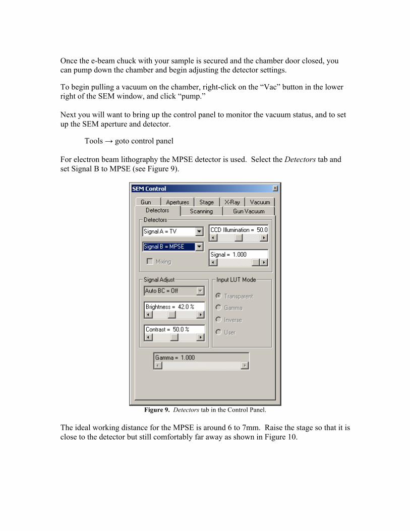
Once the e-beam chuck with your sample is secured and the chamber door closed, you can pump down the chamber and begin adjusting the detector settings. To begin pulling a vacuum on the chamber, right-click on the “Vac” button in the lower right of the SEM window, and click “pump.” Next you will want to bring up the control panel to monitor the vacuum status, and to set up the SEM aperture and detector.
Tools → goto control panel For electron beam lithography the MPSE detector is used. Select the Detectors tab and set Signal B to MPSE (see Figure 9).
Figure 9. Detectors tab in the Control Panel.
The ideal working distance for the MPSE is around 6 to 7mm. Raise the stage so that it is close to the detector but still comfortably far away as shown in Figure 10.

Figure 10. CCD view of SEM Chamber.
If it turns out later on when you are focused on the sample that the working distance is less than 6mm or greater than 7mm, you can raise or lower the stage as necessary. This rule of thumb is observed simply to establish consistency from one sample to the next. Normally, the standard 30µm aperture is used. You rarely will need to use a different aperture. One instance when you may consider using a larger one, such as the 60µm aperture, is if you are writing very big patterns. In this case, the larger aperture would reduce the amount of time for writing. Click the Apertures tab and select “30µm (see Figure 11).”

Figure 11. Apertures tab in the Control Panel.
The maximum EHT or accelerating voltage that the LEO electron microscope can supply is 30kV. For electron beam lithography, you generally want the highest accelerating voltage possible. This can be set by double-clicking on the EHT status on the “datazone” and typing in “30.” The “datazone” is the white bar along the bottom of the screen that displays the magnification, working distance, etc. Select the Vacuum tab from the Control Panel (see Figure 12). When the system vacuum reaches 2e-5 Torr turn the EHT on by right clicking on the EHT indicator in the lower right next to the vacuum indicator and clicking “EHT on.”
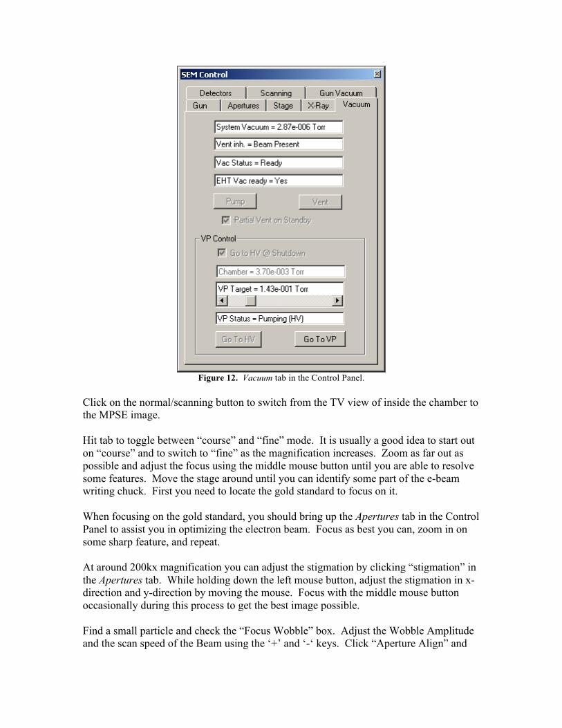
Figure 12. Vacuum tab in the Control Panel.
Click on the normal/scanning button to switch from the TV view of inside the chamber to the MPSE image. Hit tab to toggle between “course” and “fine” mode. It is usually a good idea to start out on “course” and to switch to “fine” as the magnification increases. Zoom as far out as possible and adjust the focus using the middle mouse button until you are able to resolve some features. Move the stage around until you can identify some part of the e-beam writing chuck. First you need to locate the gold standard to focus on it. When focusing on the gold standard, you should bring up the Apertures tab in the Control Panel to assist you in optimizing the electron beam. Focus as best you can, zoom in on some sharp feature, and repeat. At around 200kx magnification you can adjust the stigmation by clicking “stigmation” in the Apertures tab. While holding down the left mouse button, adjust the stigmation in x-direction and y-direction by moving the mouse. Focus with the middle mouse button occasionally during this process to get the best image possible. Find a small particle and check the “Focus Wobble” box. Adjust the Wobble Amplitude and the scan speed of the Beam using the ‘+’ and ‘-‘ keys. Click “Aperture Align” and

use left mouse button to make adjustments. The idea is to adjust the alignment such that the particle you are looking at doesn’t wobble left and right or up and down, but just in and out. Once this is done uncheck the focus wobble box and click on the mag/focus button. Before leaving the gold standard you should have focused the microscope as much as possible down to between 200kx and 300kx. Note: After going through this focusing procedure you should no longer adjust the height of the stage, the stigmation, or the aperture alignment. If you do adjust the height of the stage, you will need to go through the entire process of optimizing the beam again to ensure the best results.
5.2 Measuring the Beam Current Having focused the electron beam and optimized the stigmation and aperture alignment, the next step is to move the scan stage to find the Faraday Couple on the e-beam chuck (see Figure 13).
Figure 13. Faraday Couple.
Zoom into the hole as far as possible.
Select Tools → Goto Panel Select Specimen Current Monitor Click ’SCM On’

Allow the reading to settle and record this in your lab notebook. Using the 30µm aperture beam currents between 400 and 500pA are typical. Click ‘SCM Off’ and close the Specimen Current Monitor window. 5.3 Collecting Focus Points The next thing to do is to record the positions of the corners of your sample so that you can calculate the coordinates for the center of the sample. This set of coordinates will be used later on as the start point in your NPGS Run File. In Control Panel click the Stage tab. You can take the coordinates off of the X and Y “Go To” field (see Figure 14).
Figure 14. Faraday Couple.
To obtain the stage coordinates for a particular location, hold down alt-tab to bring up crosshairs to select the point to go to. Obtain coordinates for each of the four corners of your sample. From this data you can calculate the center of the chip by adding all of the x-components and dividing by 4 and adding all of the y-components and dividing by 4. Minimize the SEM window and run Remcon32. Make sure COM2 is selected and click the open port button (Figure 15).

Figure 15. RemCon32 Console.
This will establish the connection between NPGS and the SEM. The final task before e-beam writing is to collect datapoints for automatic focusing of the electron beam. NPGS has a script that assists you in doing this.
In NPGS select Commands → Direct Stage Control When it says “Enter Offset for Rotation Angle Calculation,” Hit “Enter” to skip. On the next screen hit Enter to Acquire New Data
Move along the edges of sample searching for small particles on which to focus. Once you find one, focus on it down to 200kx the best you can. Select the NPGS Direct Stage Control window and hit the spacebar. Repeat this to collect 4 data points, preferably near the four corners of the sample. This allows NPGS to model the surface of your sample as a plane, enabling it to estimate a working distance for any point on that plane. When done, hit “Enter.” The next screen will give you a short report and will present some options. An RMS error term less than 0.001 should be fine. Hit “Enter” to “use these results.” Afterwards you can hit “Esc” to quit. 5.4 Executing your Run File It is usually prudent to run an Error Check or Time Test on your Run File before processing it with the SEM. These utilities can be reached by clicking on “Commands” and then “Process Run File” (see Figure 16).

Figure 16. Run-File Processing Options.
In NPGS update your Run File with the beam current that you measured with the Faraday Couple and with the center coordinates that you calculated. You are finally ready to process your run file. Move beam somewhere off sample.
Tools → Goto Panel → Ext Scan Control Turn External Scan Control “on” Select the Run File and click “Process Run File”
A display will come up illustrating the progress of the e-beam writing. This information is not exactly given in real time. Sometimes it will appear that the pattern is finished being written on the screen when there may actually still be a few minutes left. When the sample is done writing, simply lower the stage and vent the chamber by right-clicking on the vacuum indicator in the lower-right corner and clicking “Vent.”

6. Conclusion You now should have a basic understanding of what goes into designing and writing a pattern using electron beam lithography. As mentioned in the introduction, this is no substitute for training with someone experienced with the process. You will likely have to put in a great deal of time to develop the experience and level of skill required to quickly and successfully write patterns that you want. If you have any questions about any of the material presented in this tutorial, do not hesitate to contact the author or Dr. Robert Krchnavek. As the e-beam process at Rowan University changes with time and as parts of this tutorial become out-of-date it is important that updates be made so that this document can continue to serve Rowan students. If you would like to make revisions, contact Dr. Robert Krchnavek for an electronic copy of the latest version of the tutorial.