electronic instrumentation - rensselaer polytechnic...
TRANSCRIPT

Electronic InstrumentationProject 4: Optical Communication Link
1. Optical Communications2. Initial Design3. PSpice Model4. Final Design
5. Project Report
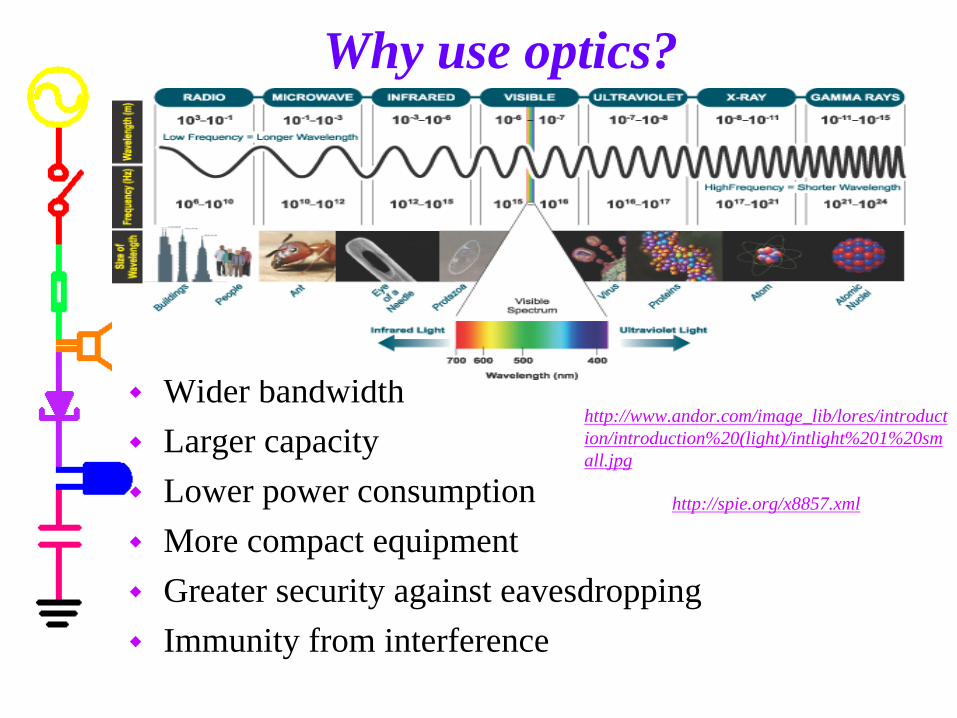
Why use optics? Advantages of optical communication
(over Radio Frequency)
Wider bandwidth
Larger capacity
Lower power consumption
More compact equipment
Greater security against eavesdropping
Immunity from interference
http://www.andor.com/image_lib/lores/introduct ion/introduction%20(light)/intlight%201%20sm all.jpg
http://spie.org/x8857.xml
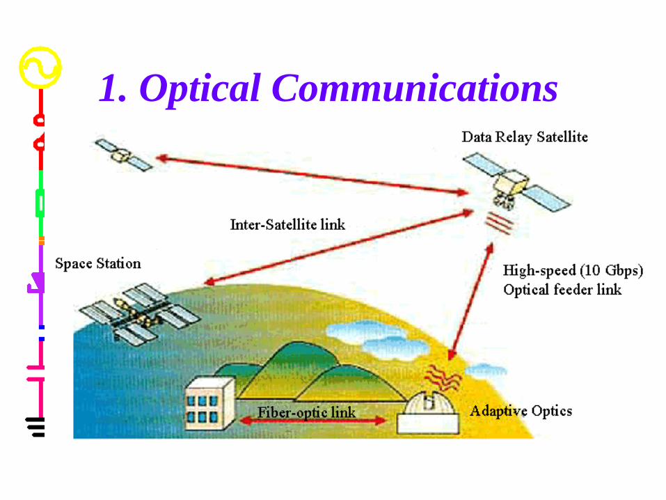
1. Optical Communications

“Lighting the way to a revolution” http://news.bbc.co.uk/1/hi/sci/tech/4671788.stm
The exponential increase of sharing information is largely due to optical communication technology
A few revolutionary technologies based on or effected by optical communication• Internet (ex. Ethernet LAN based
on Infrared Technology)• Cell phones• Satellite communication
Others?
1966 Dr. Kao andGeorge Hockham:fiber optics to carry
information with light
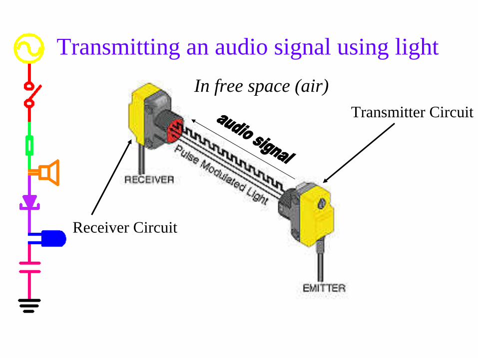
Transmitting an audio signal using light
Receiver Circuit
Transmitter CircuitIn free space (air)
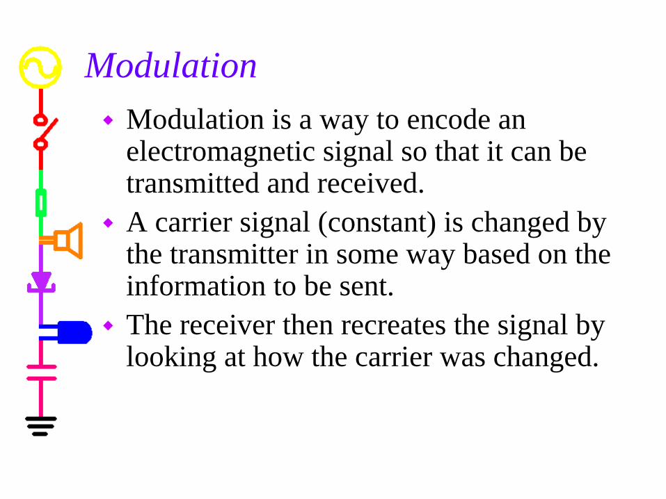
Modulation
Modulation is a way to encode an electromagnetic signal so that it can be transmitted and received.
A carrier signal (constant) is changed by the transmitter in some way based on the information to be sent.
The receiver then recreates the signal by looking at how the carrier was changed.

Modulation
Output (modulated carrier)depends on the type of modulation used
ModulatingInput signal
Carriersignal
Time
0s 4.0msV(R2:1) V(R1:1)
-4.0V
-3.0V
-2.0V
-1.0V
0V
1.0V
2.0V
3.0V
4.0V
5.0V
6.0V
7.0V
8.0V
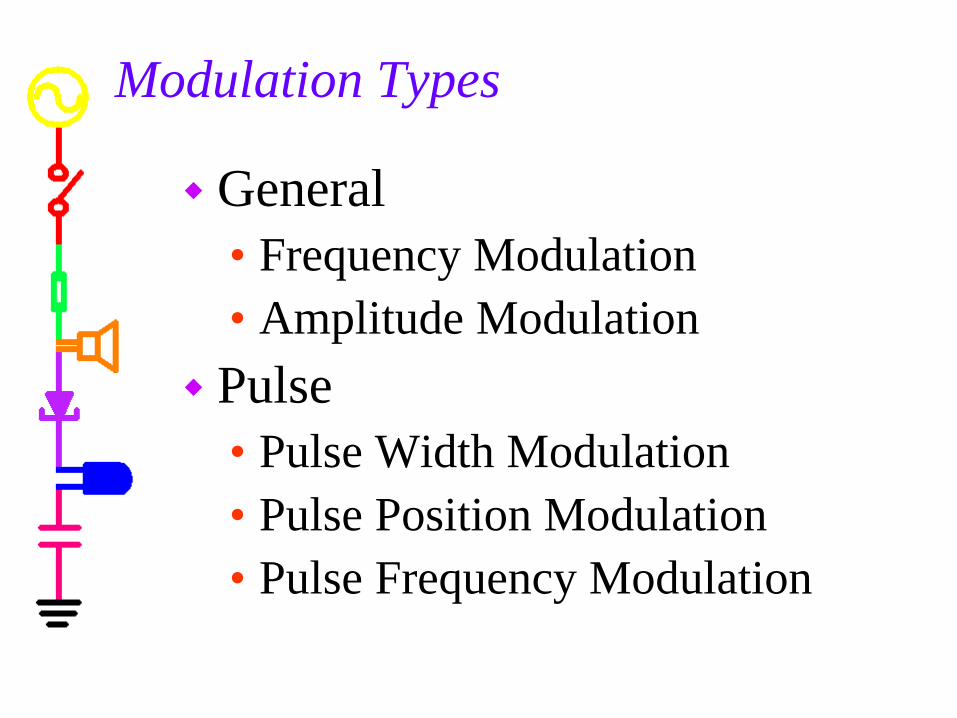
Modulation Types
General• Frequency Modulation• Amplitude Modulation
Pulse• Pulse Width Modulation• Pulse Position Modulation• Pulse Frequency Modulation

Amplitude Modulation
http://cnyack.homestead.com/files/modulation/modam.htm
Frequency of carrier remains constant.
Input signal alters amplitude of carrier.
Higher input voltage means higher carrier amplitude.
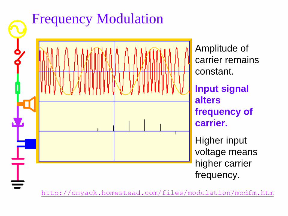
Frequency Modulation
http://cnyack.homestead.com/files/modulation/modfm.htm
Amplitude of carrier remains constant.
Input signal alters frequency of carrier.
Higher input voltage means higher carrier frequency.
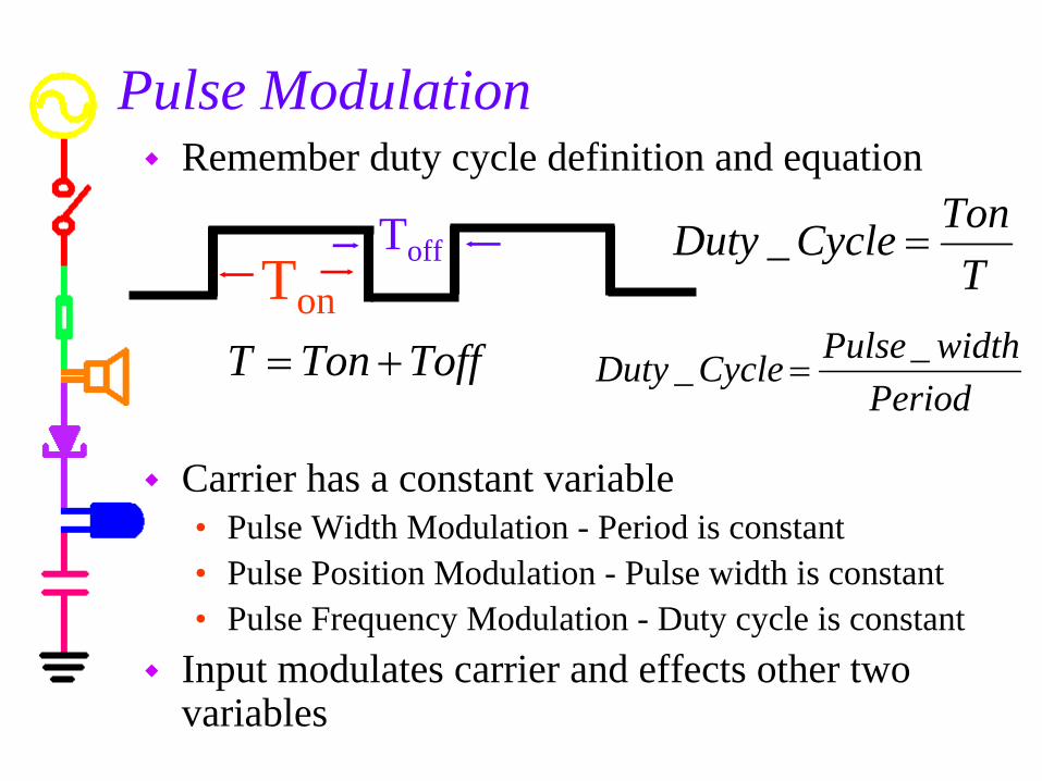
Pulse Modulation
Remember duty cycle definition and equation
Carrier has a constant variable• Pulse Width Modulation - Period is constant• Pulse Position Modulation - Pulse width is constant• Pulse Frequency Modulation - Duty cycle is constant
Input modulates carrier and effects other two variables
TTonCycleDuty _
Ton
Toff
PeriodwidthPulseCycleDuty __ ToffTonT

Pulse Width Modulation
http://cnyack.homestead.com/files/modulation/modpwm.htm
Period of carrier remains constant.
Input signal alters duty cycle and pulse width of carrier.
Higher input voltage means pulses with longer pulse widths and higher duty cycles.

Pulse Position Modulation
http://cnyack.homestead.com/files/modulation/modppm.htm
Pulse width of carrier remains constant.
Input signal alters period and duty cycle of carrier.
Higher input voltage means pulses with longer periods and lower duty cycles.

Pulse Frequency ModulationDuty cycle of carrier remains constant.
Input signal alters pulse width and period of carrier.
Higher input voltage means pulses with longer pulse widths and longer periods.

2. Initial Design
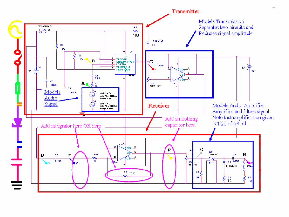
The initial design for this project is a circuit consisting of a transmitter and a receiver.
The circuit is divided into functional blocks.• Transmitter: Block A-B and Block B-C• Transmission: Block C-D• Receiver: Block D-E, Block E-F, Block F-G, and Block G-H
You will need to examine each block of the circuit.
transmitter receiver
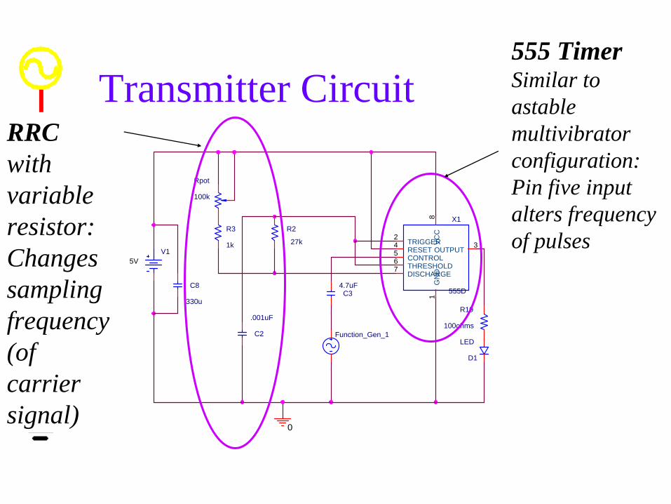
Transmitter Circuit
X1
555D
GN
D1
TRIGGER2
OUTPUT3
RESET4
CONTROL5
THRESHOLD6
DISCHARGE7
VC
C8
R2
27k
R3
1k
C2
.001uF
C34.7uF
V15V
Function_Gen_1
C8
330uR19
100ohms
D1
LED
0
Rpot
100k
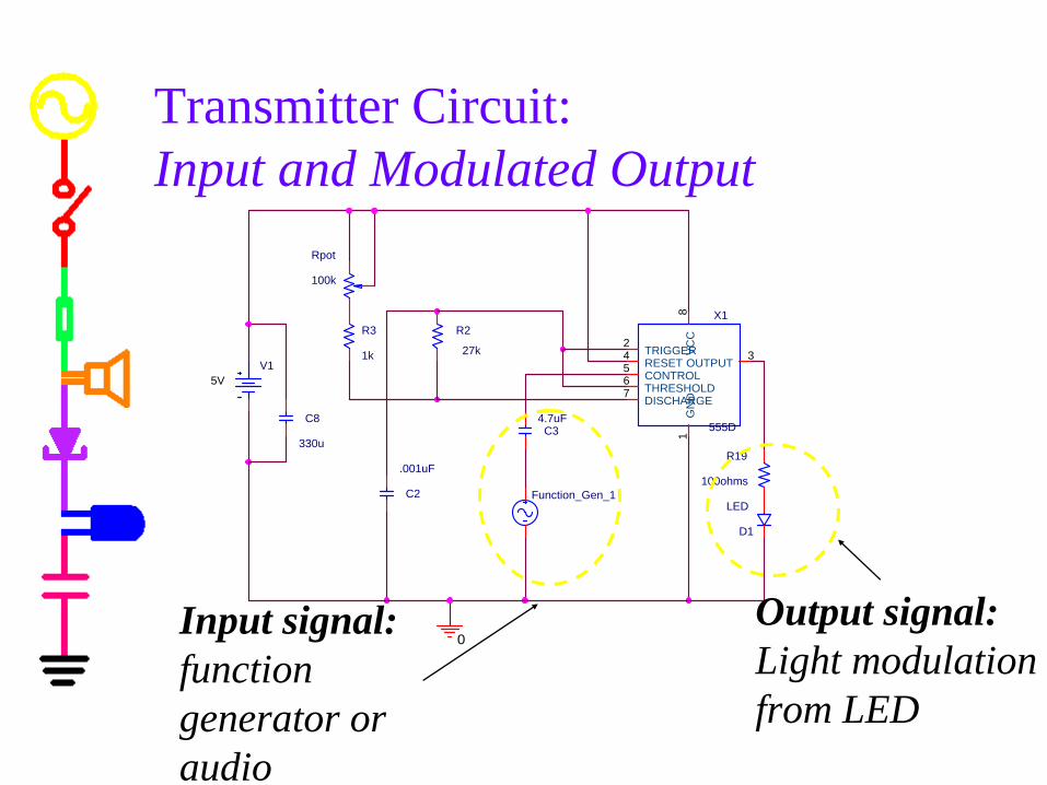
555 TimerSimilar to astable multivibrator configuration:Pin five input alters frequency of pulses
RRCwith variable resistor:Changes sampling frequency (of carrier signal)
X1
555D
GN
D1
TRIGGER2
OUTPUT3
RESET4
CONTROL5
THRESHOLD6
DISCHARGE7
VC
C8
R2
27k
R3
1k
C2
.001uF
C34.7uF
V15V
Function_Gen_1
C8
330uR19
100ohms
D1
LED
0
Rpot
100k
Transmitter Circuit: Input and Modulated Output
Input signal: function generator or audio
Output signal:Light modulationfrom LED

X1
555D
GN
D1
TRIGGER2
OUTPUT3
RESET4
CONTROL5
THRESHOLD6
DISCHARGE7
VC
C8
R2
27k
R3
1k
C2
.001uF
C34.7uF
V15V
Function_Gen_1
C8
330uR19
100ohms
D1
LED
0
Rpot
100k
Special Capacitors
Bypass Capacitor(Low Pass Filter)
DC Blocking Capacitor(High Pass Filter)Keeps DC offset from 555 Timerfrom interfering with input

Sample Input and Output
When input is higher, pulses are longer
When input is lower, pulses are shorter

Your signal is what?
The type of modulation this circuit creates is most closely categorized as pulse frequency modulation.
But the pulse width is also modulated and we will use that feature.
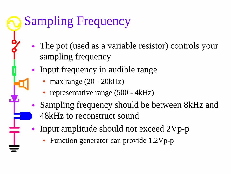
Sampling Frequency
The pot (used as a variable resistor) controls your sampling frequency
Input frequency in audible range • max range (20 - 20kHz)• representative range (500 - 4kHz)
Sampling frequency should be between 8kHz and 48kHz to reconstruct sound
Input amplitude should not exceed 2Vp-p• Function generator can provide 1.2Vp-p

Receiver Circuit
56k
Add a 100 Ohm resistor in series with the speaker to avoid failures.

Receive Light Signal
56k
Add a 100 Ohm resistor in series with the speaker to avoid failures.

Inverting Amplifier (Pre-Amp)
56k
Add a 100 Ohm resistor in series with the speaker to avoid failures.
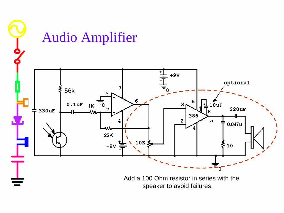
Audio Amplifier
Add a 100 Ohm resistor in series with the speaker to avoid failures.
56k

Audio Amplifier Details
volume
386 audioamplifier
low pass filter
high passfilter
increasesgain 10X(not needed)
Add a 100 Ohm resistor in series with the speaker to avoid failures.

Special Capacitors
BypassCapacitor
DC BlockingCapacitor
Add a 100 Ohm resistor in series with the speaker to avoid failures.
Not needed56k
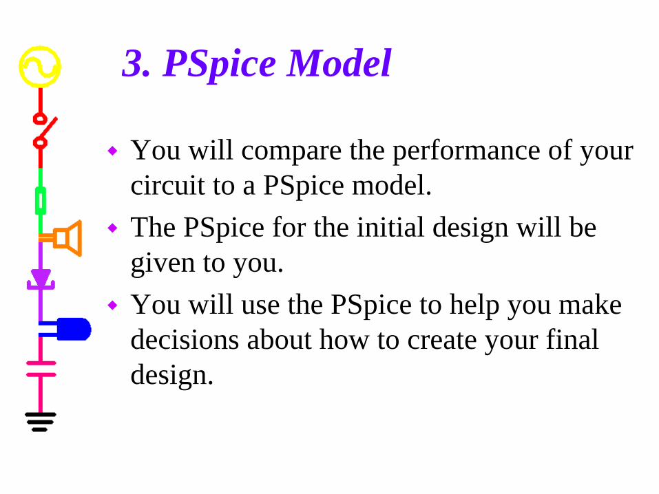
3. PSpice Model
You will compare the performance of your circuit to a PSpice model.
The PSpice for the initial design will be given to you.
You will use the PSpice to help you make decisions about how to create your final design.

Comparing Output of Blocks
Take pictures of the signal on each side of the circuit block.• A on channel 1 and B on channel 2• B on channel 1 and C on channel 2
Take all measurements relative to ground
Does the block behave as expected?
How does it compare to the PSpice output?
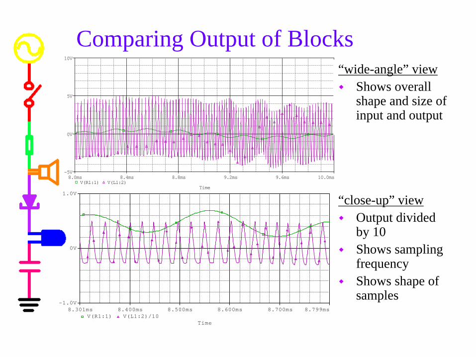
Comparing Output of Blocks
Time
8.0ms 8.4ms 8.8ms 9.2ms 9.6ms 10.0msV(R1:1) V(L1:2)
-5V
0V
5V
10V
“close-up” view
Output divided by 10
Shows sampling frequency
Shows shape of samples
Time
8.400ms 8.500ms 8.600ms 8.700ms8.301ms 8.799msV(R1:1) V(L1:2)/10
-1.0V
0V
1.0V
“wide-angle” view
Shows overall shape and size of input and output

4. Final Design
The signal is reconstructed well enough by the initial design that it will be audible.
In order to improve the quality of the signal, you will add an integrator, which will more exactly reconstruct it.
Types of integrators• passive integrator (low pass filter)• active integrator (op amp integrator circuit)
You will then improve the signal further with a smoothing capacitor.

Passive Integration
C1
R1 VoutVin
0
Integration works onlyat high frequencies f >>fc.Unfortunately,your amplitude will alsodecrease.
RCf
dtVRC
V
C
inout
21
1
Frequency
1.0Hz 10KHz 100MHzV(R1:2)
0V
250mV
500mV
E

Active Integration
CRf
dtVCR
V
fC
ini
out
21
1
• Integration works at f >>fc• Your gain goes from -Rf /Ri to -1/Ri C• The amplitude of your signal will decrease or increase depending on components
Frequency
1.0Hz 10KHz 100MHzV(R1:2)
0V
250mV
500mV
EF

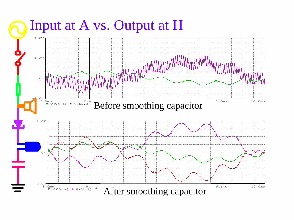
Input at A vs. Output at H
Time
8.0ms 8.4ms 8.8ms 9.2ms 9.6ms 10.0msV(R1:1) V(L1:2)
-5V
0V
5V
10V
Time
8.0ms 8.4ms 8.8ms 9.2ms 9.6ms 10.0msV(V4:+) V(L1:2)
-2.0V
0V
2.0V
4.0V
Before addition of integrator
After addition of integrator

Effect of Smoothing Capacitor
Recall what the smoothing capacitor did to the output of the half wave rectifier.
0
V
D1
D1N4148V
V1
FREQ = 1kVAMPL = 5vVOFF = 0 C1
5u
R1
1k
Time
8.0ms 8.4ms 8.8ms 9.2ms 9.6ms 10.0msV(V4:+) V(L1:2)
-2.0V
0V
2.0V
4.0V
Time
8.0ms 8.4ms 8.8ms 9.2ms 9.6ms 10.0msV(V4:+) V(L1:2) -v(L1:2)
-2.0V
0V
2.0V
Input at A vs. Output at H
Before smoothing capacitor
After smoothing capacitor

Project Packet
Initial Data with Function Generator• PSpice• Mobile Studio plots from circuit• Brief Comparison• Block Description• For
• Blocks: A-B, A-C, A-D, A-E, A-F, A-G• Overall System: A-H
Initial Data with Audio• Mobile Studio plots from circuit• For E-F and A-H

Project Packet
Final Data (integrator only) with Function Generator• PSpice• Mobile Studio plots from circuit• Brief Comparison• For E-F and A-H
Final Data (integrator and smoothing) PSpice only• PSpice• Compare to without smoothing• For E-F and A-H
Project Packet
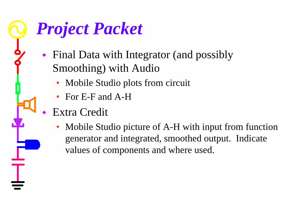
Final Data with Integrator (and possibly Smoothing) with Audio• Mobile Studio plots from circuit• For E-F and A-H
Extra Credit• Mobile Studio picture of A-H with input from function
generator and integrated, smoothed output. Indicate values of components and where used.
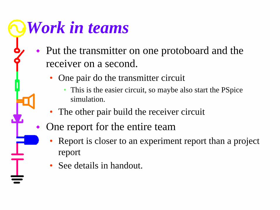
Work in teams
Put the transmitter on one protoboard and the receiver on a second.• One pair do the transmitter circuit
• This is the easier circuit, so maybe also start the PSpice simulation.
• The other pair build the receiver circuit
One report for the entire team• Report is closer to an experiment report than a project
report• See details in handout.