electronic structure and binding geometry of
TRANSCRIPT

ELECTRONIC STRUCTURE AND BINDINGGEOMETRY OF
TETRAPHENYLPORPHYRIN-DERIVEDMOLECULES ADSORBED ON METAL AND METAL
OXIDE SURFACES
BY SENIA COH
A dissertation submitted to the
Graduate School—New Brunswick
Rutgers, The State University of New Jersey
in partial fulfillment of the requirements
for the degree of
Doctor of Philosophy
Graduate Program in Physics and Astronomy
Written under the direction of
Professor Robert A. Bartynski
and approved by
New Brunswick, New Jersey
October, 2012

ABSTRACT OF THE DISSERTATION
Electronic structure and binding geometry of
tetraphenylporphyrin-derived molecules adsorbed on
metal and metal oxide surfaces
by Senia Coh
Dissertation Director: Professor Robert A. Bartynski
Tetraphenylporphyrin (TPP)-derived molecules have been studied extensively as efficient pho-
tosensitizers when chemisorbed on the metal oxide substrates in dye-sensitized solar cells. Still,
many fundamental electronic properties of the dye/oxide interface are not understood and need
careful consideration. In this thesis we present a comprehensive study of the electronic structure,
energy level alignment and the adsorption geometry of the TPP-derived dye molecules adsorbed
on TiO2(110), ZnO(1120) and Ag(100) single crystal surfaces using ultra-high vacuum (UHV)
based surface sensitive techniques.
The alignment of the molecular energy levels with respect to the TiO2 and ZnO band edges
for all TPP-derived molecules we studied was found to be insensitive to either the nature of
the functional groups located on the phenyl rings, presence of zinc as a central metal ion and
different binding geometry of the molecules. Binding geometry, molecule-molecule interaction
and the aggregation effects in the adsorbed layer, that were observed in the UV-visible spectra
of the molecules adsorbed on ZnO substrate were not observed in the ultraviolet photoemission
ii
(UPS) and inverse photoemission (IPS) spectra of the occupied and unoccupied molecular states.
Using near edge X-ray absorption fine structure (NEXAFS) and scanning tunneling microscopy
(STM), binding geometry of the two representative TPP-derivatives was directly determined
to be upright, with the porphyrin ring under large angle with respect to the surface for the
p-ZnTCPP molecules and with the porphyrin ring parallel to the surface for the m-ZnTCPP
molecules.
We observe that the energies and the energy level alignment of the ZnTPP molecular lev-
els measured in UPS and IPS depend on the substrate on which the molecules are adsorbed
(Ag(100) or TiO2(110) single crystal surfaces). The differences are attributed to different charge
screening properties of these two materials. Image charges created in the substrates during the
measurement affect both the ground state electronic structure and the electronic excitations in
the molecules causing the transport gap, the optical gap and the exciton binding energy of the
molecules to decrease as the thickness of the film decreases. As measured in STM, the molecules
in the first layer adsorb with the porphyrin rings parallel to the surface, while the phenyl rings
are essentially upright on both surfaces.
iii

Acknowledgements
These past six years at Rutgers had been such a wonderful time and there are so many people
I would like to thank for that. First and foremost, I’m deeply grateful to my advisor, Bob
Bartynski on his guidance and kindness, especially when challenges arose. His knowledge and
scientific intuition have always amazed me. I would like to thank Sylvie for her guidance and
patience throughout my Ph.D. and for teaching me that there is always a different perspective.
My past and present lab mates were absolutely great and I would like to thank them for their
support. Thank you Eric, Levan, Ryan, Chaz and Grant. The lab was a great place to work
with you around. I’m grateful to Boris, Wenhua, Quantong and Leszek for their support and
for being so welcoming and helpful, especially whenever I needed to borrow some ultra-high
vacuum parts. I would like to thank Gwen for her support, warmheartedness and for being such
great secretary with great organizational skills. I’m thankful that we have such skilled team of
machinists in the machine shop at the Physics Department. Thank you Bill, Arvid, Eric and
Ernie. It was always enjoyable working with you.
I would like to thank our collaborators in Elena Galoppini’s group at Chemistry Department
at Rutgers, Newark for interesting discussions that were very helpful in understanding many
chemistry-related details that came along the way. I’m grateful to my committee members,
Premi Chandra, Misha Gershenson and Terry Matilsky and to Ron Ransome for their guidance,
especially during the hardest time in my Ph.D. when I had to switch my advisors.
My Ph.D. would absolutely wouldn’t be anything close to what it was if it wasn’t for
my friends. Thank you Aatish, Adina, Andrei, Alexey, Andy, Anil, Anindya, Anthony, Am-
ruta, Ashlee, Bumsu, Beth, Daniel, Darakhshan, Deepak, Can, Chen, Chioun, Eammon, Erin,
iv

George, Hang Dong, Hyowon, Ilya, James, Jiyeon, John, Kasturi, Kshitij, Kyoo, Lisa, Lu-
cia, Lizzie, Madel, Manjul, Marietta, Maryam, Patrick, Qibin, Ray, Rebecca, Ritvik, Robin,
Roberto, Sung Po, Sushmita, Takeshi, Vandana, Vijay, Yanan, Yi, Yuval, Xueyun. I would
especially like to thank Chuck for being such a great friend and support during both easy and
hard times during my Ph.D..
I would like to thank my mom and my dad for being always there for me and being supportive
of what I do and to all of my family members. Thank you for your unconditional love.
And last but not least, to the two most important men in my life. Thank you, Sinisa for
your never ending love and support throughout my Ph.D.. Thank you for staying home and
putting your research on hold so I can finish my thesis. Thank you, Benjamin for bringing
smiles to our lives and for reminding us where is the greatest joy of all. Love you both with all
my heart.
v

Dedication
To my family
vi

Table of Contents
Abstract . . . . . . . . . . . . . . . . . . . . . . . . . . . . . . . . . . . . . . . . . . . . ii
Acknowledgements . . . . . . . . . . . . . . . . . . . . . . . . . . . . . . . . . . . . . iv
Dedication . . . . . . . . . . . . . . . . . . . . . . . . . . . . . . . . . . . . . . . . . . . vi
List of Tables . . . . . . . . . . . . . . . . . . . . . . . . . . . . . . . . . . . . . . . . . . x
List of Figures . . . . . . . . . . . . . . . . . . . . . . . . . . . . . . . . . . . . . . . . . xi
1. Introduction and motivation . . . . . . . . . . . . . . . . . . . . . . . . . . . . . . 1
1.1. Organic photovoltaics: a general scope . . . . . . . . . . . . . . . . . . . . . . . . 1
1.2. Dye-sensitized solar cells . . . . . . . . . . . . . . . . . . . . . . . . . . . . . . . . 3
1.3. Interfaces that contain organic molecules . . . . . . . . . . . . . . . . . . . . . . . 13
1.4. Thesis Outline . . . . . . . . . . . . . . . . . . . . . . . . . . . . . . . . . . . . . 25
2. Experimental and theoretical methods . . . . . . . . . . . . . . . . . . . . . . . . 27
2.1. Introduction . . . . . . . . . . . . . . . . . . . . . . . . . . . . . . . . . . . . . . . 27
2.2. Ultra High Vacuum (UHV) . . . . . . . . . . . . . . . . . . . . . . . . . . . . . . 28
2.3. Photoemission Spectroscopy . . . . . . . . . . . . . . . . . . . . . . . . . . . . . . 31
2.4. Inverse Photoemission Spectroscopy . . . . . . . . . . . . . . . . . . . . . . . . . 41
2.5. Scanning Tunneling Microscopy . . . . . . . . . . . . . . . . . . . . . . . . . . . . 50
2.6. UV-visible Absorption Spectroscopy . . . . . . . . . . . . . . . . . . . . . . . . . 52
2.7. Reflection Electron Energy Loss Spectroscopy . . . . . . . . . . . . . . . . . . . . 57
2.8. Near-Edge X-ray Absorption Fine Structure . . . . . . . . . . . . . . . . . . . . . 63
2.9. Computational methods . . . . . . . . . . . . . . . . . . . . . . . . . . . . . . . . 68
vii

3. Electronic structure, energy alignment and molecular packing of zinc(II)te-
traphenylporphyrin derivatives adsorbed on TiO2(110) and ZnO(1120) surfaces 70
3.1. Introduction . . . . . . . . . . . . . . . . . . . . . . . . . . . . . . . . . . . . . . . 70
3.2. Experimental . . . . . . . . . . . . . . . . . . . . . . . . . . . . . . . . . . . . . . 73
3.3. Results and discussion . . . . . . . . . . . . . . . . . . . . . . . . . . . . . . . . . 75
3.4. Conclusion . . . . . . . . . . . . . . . . . . . . . . . . . . . . . . . . . . . . . . . 93
4. Electronic structure and energy level alignment of free-base and zinc tetraphenyl-
porphyrin molecules on ZnO(1120) . . . . . . . . . . . . . . . . . . . . . . . . . . . . 95
4.1. Introduction . . . . . . . . . . . . . . . . . . . . . . . . . . . . . . . . . . . . . . . 95
4.2. Experimental Methods and Sample Preparation . . . . . . . . . . . . . . . . . . . 99
4.3. Computational Methods . . . . . . . . . . . . . . . . . . . . . . . . . . . . . . . . 100
4.4. Results and discussion . . . . . . . . . . . . . . . . . . . . . . . . . . . . . . . . . 100
4.5. Conclusion . . . . . . . . . . . . . . . . . . . . . . . . . . . . . . . . . . . . . . . 116
5. Electronic structure, adsorption geometry and energy level alignment of
zinc(II)tetraphenylporphyrin molecules evaporated onto Ag(100) and TiO2(110)
surfaces . . . . . . . . . . . . . . . . . . . . . . . . . . . . . . . . . . . . . . . . . . . . . 117
5.1. Introduction . . . . . . . . . . . . . . . . . . . . . . . . . . . . . . . . . . . . . . . 117
5.2. Experimental methods and sample preparation . . . . . . . . . . . . . . . . . . . 120
5.3. Computational . . . . . . . . . . . . . . . . . . . . . . . . . . . . . . . . . . . . . 121
5.4. Results and discussion . . . . . . . . . . . . . . . . . . . . . . . . . . . . . . . . . 122
5.5. Conclusion . . . . . . . . . . . . . . . . . . . . . . . . . . . . . . . . . . . . . . . 151
Bibliography . . . . . . . . . . . . . . . . . . . . . . . . . . . . . . . . . . . . . . . . . . 154
Appendix A. UPS spectrum calibration and work function measurement . . . 167
A.1. UPS spectrum calibration . . . . . . . . . . . . . . . . . . . . . . . . . . . . . . . 167
A.2. Obtaining the work function and the ionization potential using UPS . . . . . . . 169
viii

Appendix B. Inverse photoemission spectrum calibration . . . . . . . . . . . . . . 173
Appendix C. UV-visible absorption spectrum of the organic molecules . . . . . 176
C.1. Ground and excited states of the organic molecules . . . . . . . . . . . . . . . . . 176
C.2. Aggregation and molecular exciton coupling model . . . . . . . . . . . . . . . . . 179
Appendix D. Gouterman four-orbital model . . . . . . . . . . . . . . . . . . . . . . 181
Appendix E. Molecular orientation determination using NEXAFS . . . . . . . . 187
Appendix F. Density functional theory basics and basis sets . . . . . . . . . . . . 193
F.1. The many-body problem . . . . . . . . . . . . . . . . . . . . . . . . . . . . . . . . 193
F.2. Basis sets in quantum chemistry calculations . . . . . . . . . . . . . . . . . . . . 199
Vita . . . . . . . . . . . . . . . . . . . . . . . . . . . . . . . . . . . . . . . . . . . . . . . 203
ix

List of Tables
2.1. Vacuum types and corresponding pressure ranges . . . . . . . . . . . . . . . . . . 29
3.1. Calculated frontier orbital energies in eV and their respective symmetries. . . . . 78
3.2. Position of HOMO-1/HOMO and LUMOs centroids extracted from the experi-
mental spectra measured on sensitized TiO2(110) and resulting energy gap. . . . 84
4.1. Calculated frontier orbitals energies in eV and their respective symmetry. . . . . 110
4.2. HOMO-1/HOMO and LUMOs centroids extracted from the experimental spectra
and resulting peak to peak energy gap of the four TCPP considered in this study. 115
5.1. Energy positions of features in UPS and IPS spectra of ZnTPP/Ag(100) with
annealing temperature in eV . . . . . . . . . . . . . . . . . . . . . . . . . . . . . 138
5.2. Energy positions of features in UPS and IPS spectra of ZnTPP/TiO2(110) with
annealing temperature in eV . . . . . . . . . . . . . . . . . . . . . . . . . . . . . 140
5.3. Transport and optical gaps and the exciton binding energies in eV for ZnTPP/Ag(100)151
5.4. Transport and optical gaps and the exciton binding energies in eV for ZnTPP/TiO2(110)151
x

List of Figures
1.1. Schematic of the dye-sensitized solar cell structure. . . . . . . . . . . . . . . . . . 4
1.2. Schematic of the charge transfer processes in dye-sensitized solar cell. . . . . . . . 5
1.3. Chemical structures of (a) porphyrin, (b) zinc porphyrin, (c) ZnTPP, (d) p-
ZnTCPP, (e) ZnTMP-Ipa, (f) ZnTXPSCA molecules. . . . . . . . . . . . . . . . 9
1.4. Schematic of the binding modes of the COOH anchoring group to the metal oxide
surface. . . . . . . . . . . . . . . . . . . . . . . . . . . . . . . . . . . . . . . . . . 11
1.5. Chemical structure of the (a) p-H2TCPP, (b) p-ZnTCPP and (c) N3 dye molecules. 11
1.6. Schematic of the electrostatic potential of an atom, a molecule and a molecular
solid. . . . . . . . . . . . . . . . . . . . . . . . . . . . . . . . . . . . . . . . . . . . 16
1.7. Schematic of the surface dipole in metals. . . . . . . . . . . . . . . . . . . . . . . 18
1.8. Schematic of energy levels in the organic semiconductor upon formation of the
interface with a metal. . . . . . . . . . . . . . . . . . . . . . . . . . . . . . . . . . 19
1.9. Schematic of the energy level alignment at metal/organic interfaces with band
bending. . . . . . . . . . . . . . . . . . . . . . . . . . . . . . . . . . . . . . . . . . 22
1.10. Schematic of the important energy alignment parameters for the metal oxide and
the organic semiconductor. . . . . . . . . . . . . . . . . . . . . . . . . . . . . . . 23
1.11. Schematic of the two regimes at the oxide/organic semiconductor interface, (a)
ϕ > IEorg and (b) ϕ < IEorg. . . . . . . . . . . . . . . . . . . . . . . . . . . . . . 24
2.1. Vacuum pumps that are used to achieve ultra-high vacuum. (a) Rotary vane
pump, (b) turbo pump and (c) ion pump. . . . . . . . . . . . . . . . . . . . . . . 29
2.2. Schematic diagram of the photoemission process for two electrons with different
initial energies. . . . . . . . . . . . . . . . . . . . . . . . . . . . . . . . . . . . . . 32
xi

2.3. Universal curve of the electron inelastic mean free path (IMFP) with respect to
the electron energy. . . . . . . . . . . . . . . . . . . . . . . . . . . . . . . . . . . . 33
2.4. Schematic diagram of a double-pass cylindrical mirror analyzer (CMA). . . . . . 38
2.5. Schematic diagram of a channeltron electron multiplier and the current to voltage
conversion circuit. . . . . . . . . . . . . . . . . . . . . . . . . . . . . . . . . . . . 39
2.6. Schematic diagram of a single electron inverse photoemission process. . . . . . . 42
2.7. Schematic energy diagram of an electron gun and a sample in the inverse pho-
toemission spectroscopy. . . . . . . . . . . . . . . . . . . . . . . . . . . . . . . . . 44
2.8. Schematic diagram and basic properties of a concave spherical diffraction grating. 45
2.9. Schematic diagram of the grating spectrometer IPS system in our UHV chamber. 46
2.10. Schematic diagram of a 2D position sensitive photon detector. . . . . . . . . . . . 48
2.11. Schematic diagram of the scanning tunneling microscopy instrumentation. . . . . 51
2.12. Schematic diagram of the UV-visible absorption spectroscopy instrumentation. . 54
2.13. Typical UV-visible absorption spectra of (a) free-base tetraphenylporphyrin and
(b) zinc tetraphenylporphyrin in methanol. . . . . . . . . . . . . . . . . . . . . . 56
2.14. Schematic of the transitions for (a) zinc and (b) free-base tetraphenylporphyrin
molecules assigned to their UV-visible absorption spectra features. . . . . . . . . 57
2.15. Schematic diagram of a single electron excitation and de-excitation processes in
solids. . . . . . . . . . . . . . . . . . . . . . . . . . . . . . . . . . . . . . . . . . . 59
2.16. A typical shape of REELS spectrum. . . . . . . . . . . . . . . . . . . . . . . . . . 60
2.17. Schematic diagram of scattering processes in a solid during REELS measurements. 61
2.18. Schematic diagram of the arrangement of the sample, electron gun and the elec-
tron analyzer for REELS in our UHV chamber. . . . . . . . . . . . . . . . . . . . 62
2.19. Schematic diagram of the origin of NEXAFS features for a diatomic molecule. . . 64
2.20. Schematic diagram of electron excitation and de-excitation processes in NEXAFS. 66
2.21. Schematic diagram of a partial electron yield detector. . . . . . . . . . . . . . . . 68
xii

3.1. The four ZnTPP derivatives considered in this study. . . . . . . . . . . . . . . . . 73
3.2. (a)Calculated DOS for the Ipa, PhCOOH, Ph, Mes and ZnP moities compared
to the (b) calculated DOS of the ZnTPP derivatives considered here. In both
graphs, the two arrows indicate the nearly degenerate HOMO-1/HOMO and
LUMOs centroid positions of a ZnP molecule. The dashed lines are aligned with
the degenerate HOMOs and LUMOs of a benzene molecule. . . . . . . . . . . . . 77
3.3. UPS (energy< 0 eV) and IPS (energy> 0 eV) spectra of clean (a) TiO2(110) and
(b) ZnO(11-20) sample. . . . . . . . . . . . . . . . . . . . . . . . . . . . . . . . . 79
3.4. An example of the subtraction procedure and obtaining the ZnTPP-Ipa molecular
contribution to the UPS and IPS spectra. . . . . . . . . . . . . . . . . . . . . . . 80
3.5. Molecular contribution to the measured UPS and IPS spectra extracted from the
sensitized (a) TiO2(110) and (b) ZnO(1120) surfaces. (c) Rescaled calculated
DOS for each ZnTPP derivative. . . . . . . . . . . . . . . . . . . . . . . . . . . . 81
3.6. Energy diagram at the ZnTPP derivative/oxide interfaces for TiO2(110) and
ZnO(1120). . . . . . . . . . . . . . . . . . . . . . . . . . . . . . . . . . . . . . . . 82
3.7. Gaussian fit of HOMOs and LUMOs features in the (a) UPS and the (b) IPS
spectra of ZnTPP-Ipa molecule . . . . . . . . . . . . . . . . . . . . . . . . . . . . 83
3.8. NEXAFS spectra of the m-ZnTCPP molecule adsorbed onto TiO2(110) and
ZnO(1120) at the C 1s (a) and (c) and the N 1s (b) and (d) edges as a function
of the light incidence angle θ. . . . . . . . . . . . . . . . . . . . . . . . . . . . . . 86
3.9. NEXAFS spectra of p-ZnTCPP adsorbed onto TiO2(110) and ZnO(1120) at the
C 1s (a) and (c) and the N 1s (b) and (d) edges as a function of the light incidence
angle θ. . . . . . . . . . . . . . . . . . . . . . . . . . . . . . . . . . . . . . . . . . 88
xiii

3.10. (a) Unoccupied states measured in STM (U=1.6V, I=1nA) of an ordered pivalate
layer on a TiO2(110) surface before sensitization. (b) and (c) STM image of the
surface sensitized with m-ZnTCPP in unoccupied states (U=2V, I=1nA). (d)
Adsorption geometries of both the pivalate layer and the m-ZnTCPP molecules
are proposed in the side view and top view schematics of a TiO2(110) surface. . . 89
3.11. A representative STM image of TiO2 surface sensitized with p-ZnTPP molecules. 90
3.12. UV-visible absorption spectra measured on TiO2 nanoparticles sensitized withm-
ZnTCPP and p-ZnTCPP. The dipoles formed upon photoexcitation are indicated
by green arrows in a schematic. . . . . . . . . . . . . . . . . . . . . . . . . . . . . 91
3.13. (a) Incident photon to current efficiency (IPCE) obtained from devices using
TiO2 nanoparticles sensitized with m-ZnTCPP and p-ZnCTPP (b) Main de-
excitation channel for a photoexcited m-ZnTCPP: electron injection into the
substrate conduction band. (c) Additional de-excitation channel enabled by the
stacked geometry of the p-ZnTCPP molecules: exciton delocalization through
dipole-dipole interaction. . . . . . . . . . . . . . . . . . . . . . . . . . . . . . . . . 93
4.1. Chemical structure of the TCPP derivatives in this study. . . . . . . . . . . . . . 97
4.2. UV-visible absorption spectra of (a)m-ZnTCPP, p-ZnTCPP and (b)m-H2TCPP,
p-H2TCPP molecules in methanol. . . . . . . . . . . . . . . . . . . . . . . . . . . 102
4.3. UV-visible absorption spectra of (a)m-ZnTCPP, p-ZnTCPP and (b)m-H2TCPP,p-
H2TCPP molecules bonded to ZnO nanoparticle thin film. . . . . . . . . . . . . . 103
4.4. UPS and IPS spectra of a clean ZnO(11-20) single crystal and ZnO sensitized
with m-H2TCPP, m-ZnTCPP, p-H2TCPP and p-ZnTCPP molecules. . . . . . . 104
4.5. UPS and IPS spectra of the adsorbed m-H2TCPP, m-ZnTCPP, p-H2TCPP and
p-ZnTCPP molecules. . . . . . . . . . . . . . . . . . . . . . . . . . . . . . . . . . 105
4.6. Calculated geometries of the p-H2TCPP and the m-ZnTCPP molecules opti-
mized in the C4v and C2v symmetries, respectively. . . . . . . . . . . . . . . . . . 107
xiv

4.7. Calculated electronic states for the m-H2TCPP, m-ZnTCPP, p-H2TCPP and
p-ZnTCPP molecules. . . . . . . . . . . . . . . . . . . . . . . . . . . . . . . . . . 108
4.8. Calculated electronic structure for the m-H2TCPP, m-ZnTCPP, p-H2TCPP and
p-ZnTCPP molecules broadened with the 1.2 eV full width at half maximum
Gaussian function. . . . . . . . . . . . . . . . . . . . . . . . . . . . . . . . . . . . 109
4.9. UPS and IPS spectra of the adsorbed m-H2TCPP, m-ZnTCPP, p-H2TCPP and
p-ZnTCPP molecules. . . . . . . . . . . . . . . . . . . . . . . . . . . . . . . . . . 112
4.10. Gaussian fit of HOMO-1/HOMO feature in the UPS spectrum of m-ZnTCPP
molecule. . . . . . . . . . . . . . . . . . . . . . . . . . . . . . . . . . . . . . . . . 113
4.11. (a) Comparison of the experimental occupied and unoccupied states of the m-
ZnTCPP molecule compared to its gas phase calculated DOS. (b) Energy level
alignment between the HOMOs/LUMOs of the m-ZnTCPP dye with respect to
the valence and conduction band edges of the ZnO(1120) single crystal. . . . . . 115
5.1. Chemical structure of the ZnTPP molecule. . . . . . . . . . . . . . . . . . . . . . 118
5.2. (a) C 1s XPS spectra of ZnTPP/Ag(100) taken at different annealing temper-
atures. The peak shifts with temperature indicating multilayer desorption. (b)
ZnTPP/Ag(100) film thickness at different annealing temperatures. . . . . . . . . 123
5.3. STM images and proposed model of adsorption in the first layer of ZnTPP
molecules adsorbed on Ag(100). . . . . . . . . . . . . . . . . . . . . . . . . . . . . 125
5.4. STM images and proposed model of adsorption in the first layer of ZnTPP
molecules adsorbed on TiO2(110). . . . . . . . . . . . . . . . . . . . . . . . . . . 127
5.5. Electronic DOS of the ZnTPP molecule. . . . . . . . . . . . . . . . . . . . . . . . 130
5.6. UPS and IPS spectra of (a) clean Ag(100) and ZnTPP/Ag(100) samples and (b)
clean TiO2 and ZnTPP/TiO2 samples after annealing at indicated temperatures. 132
5.7. Calculated DOS of ZnTPP in gas phase and molecular contribution to UPS and
IPS spectra of (a) ZnTPP/Ag(100) and (b) ZnTPP/TiO2(110) samples after
annealing at indicated temperatures. . . . . . . . . . . . . . . . . . . . . . . . . . 134
xv

5.8. Change in energies of the HOMOs and LUMOs with the annealing temperature. 139
5.9. The secondary electron cutoff in UPS He I for (a) clean Ag(100) and ZnTPP/Ag(100)
and (b) clean TiO2(110) and ZnTPP/TiO2(110) . . . . . . . . . . . . . . . . . . 143
5.10. Energy level alignment diagram for 1 ML of ZnTPP on (a) Ag(100) and (b)
TiO2(110) . . . . . . . . . . . . . . . . . . . . . . . . . . . . . . . . . . . . . . . . 144
5.11. REELS spectra of ZnTPP film deposited on (a) Ag(100) and (b) TiO2(110) . . . 147
5.12. Schematic of the transport gap, optical gap and the exciton binding energy of an
organic film as a function of a distance from the metallic substrate. . . . . . . . . 150
A.1. He II UPS spectrum of (a) gold and (b) TiO2(110) sample. . . . . . . . . . . . . 167
A.2. Schematic diagram of the spectrum width measurement. . . . . . . . . . . . . . . 170
A.3. Schematic energy diagram showing the most important quantities for (a) a metal-
lic and (b) an insulating sample. . . . . . . . . . . . . . . . . . . . . . . . . . . . 172
B.1. Schematic energy diagram of an electron gun and a sample in the inverse pho-
toemission spectroscopy. . . . . . . . . . . . . . . . . . . . . . . . . . . . . . . . . 174
B.2. An example of the detector response function. . . . . . . . . . . . . . . . . . . . . 175
C.1. Schematic diagram illustrating the formation of the σ, π, σ∗ and π∗ orbitals from
p orbitals on two carbon atoms. . . . . . . . . . . . . . . . . . . . . . . . . . . . . 177
C.2. Schematic molecular energy diagram with the transitions between occupied and
unoccupied states. . . . . . . . . . . . . . . . . . . . . . . . . . . . . . . . . . . . 178
C.3. Schematic energy diagram of the singlet and triplet excited states. . . . . . . . . 178
C.4. Schematic diagram of (a) H- and (b) J-aggregates and corresponding excited states.180
D.1. An example of the porphyrin UV-visible absorption spectrum. . . . . . . . . . . . 181
D.2. Schematic diagram of two lowest occupied (b1 and b2) and unoccupied (c1 and
c2) orbitals of a free-base porphyrin molecule. . . . . . . . . . . . . . . . . . . . . 183
E.1. Carbon K-edge NEXAFS spectra of the benzene molecule adsorbed on Ag (110)
surface recorded under both grazing and normal X-ray incidence angles. . . . . . 190
xvi

E.2. Angles considered in the derivation of the angular dependance of the NEXAFS
intensity. . . . . . . . . . . . . . . . . . . . . . . . . . . . . . . . . . . . . . . . . . 191
xvii
1
Chapter 1
Introduction and motivation
1.1 Organic photovoltaics: a general scope
Fossil fuels (oil, natural gas and coal) have been the main energy sources of mankind since the
first industrial revolution and have led to remarkable technological, economical and cultural
growth. However, burning fossil fuels is not sustainable, since the abundance of these fuels
on Earth is limited and also because the by-products of burning process contribute to the
greenhouse effect and global warming. More sustainable energy sources are needed to provide
for the growing energy demand of the mankind. Today, the most efficient way to produce
energy is in nuclear power plants. However, nuclear power plants are potentially hazardous in
case of the malfunction and they also produce long lived radioactive by-products that need to
be properly stored.
An alternative energy source that is more sustainable and nearly unlimited is the Sun. A
part of the light from the Sun that reaches the Earth’s surface can be converted into electricity
by using the photovoltaic, or solar cells. This idea is not new. The first modern silicon single
crystal solar cell with a power conversion efficiency of 6% was first invented and built by D.
Chapin, C. S. Fuller and G. Pearson[1] in 1954 at Bell Labs. A few years later researchers
brought up the efficiency of the silicon solar cell to 15 %. Nowadays, silicon dominates the solar
cell market, with 98 % of all solar cells using silicon for photovoltaic conversion.
However, the primary problem with using silicon as an active material in the solar cells is
the cost of the material. Silicon is not an ideal material for the photovoltaic conversion. It is
an indirect bandgap material, which means that the conduction band minimum and valence

2
band maximum of silicon are not situated at the same k-points. This requires a change of
the momentum of an excited electron in the material that an incoming photon cannot provide.
Consequently, light absorption in silicon is impeded and a thick layer of silicon (on the order of
100 µm) is required for efficient absorption. This, furthermore, increases the cost of solar cell
production. Moreover, processing of the material requires high temperatures, while impurity
and dopant levels need to be strictly controlled to produce a high quality silicon material.
The search for a more suitable and cheaper materials for solar cells started almost with
the beginnings of the solar cell technology. Recently, organic materials have emerged as poten-
tially suitable materials for the solar cells. Organic materials offer a wide variety of advantages
compared to the traditional inorganic semiconductors, mainly in the area of low density, me-
chanical flexibility, direct bandgaps for optical excitations and solution-based low temperature
processing that is suitable for large area solar cell production. Furthermore, the functionality
of the organic materials can be tuned at the molecular level, where small modifications of the
molecules can change dramatically both the electronic and the optical properties as well as the
molecule/molecule interaction when adsorbed on a substrate. One type of organic solar cells are
the ones in which two organic semiconductors, one that is an electron donor and another one
that is an electron acceptor, are brought together to form a junction. However, in these types of
organic solar cells, device architecture deviates significantly from planar hetero or homojunction
solar cells usually seen in the inorganic devices. Since the exciton diffusion length is small in
the organic semiconductors, to increase the exciton dissociation rate and thus the cell efficiency,
the idea of bulk distributed interface, or bulk heterojunction, have been employed. Another
type of the organic solar cells are the hybrid solar cells, that are also called dye-sensitized solar
cells (DSSCs), in which the organic dye molecules are chemisorbed onto the conducting nanos-
tructured metal oxide thin film from solution and act as the photoabsorbers. Up to date, the
highest efficiency of all-organic solar cells is 10.7 % achieved in German company Heliatek[2],
whereas the highest DSSC efficiencies are around 13 %[3].
Despite these successes of DSSCs reported so far, a great majority of research in the field is

3
based on the “trial and error” approach. Controlled studies of the key parameters that influence
the energy level alignment and the electronic structure at the dye/oxide interface would be thus
extremely valuable in further improvement of the DSSC performance.
In the next following sections we will focus more on the dye-sensitized solar cells and explain
the components, energetics and processes in the cell in more detail.
1.2 Dye-sensitized solar cells
1.2.1 Components and processes in the dye-sensitized solar cells
At the heart of the dye-sensitized solar cell (DSSC) is a nanostructured metal oxide thin film
with transition metal or all-organic dye molecules chemisorbed on the oxide surface. This type
of solar cell was invented by Gratzel in 1991 when the photovoltaic effect was demonstrated for
the cell containing a Ru-based organic dye and a nanoporous TiO2 thin film[4].
The cell itself is constructed as shown in Fig. 1.1. The bottom electrode consists of glass
plate coated with the transparent conducting oxide (TCO), which is typically SnO2 doped with
fluorine. The TCO layer serves as an electrode but it also transmits more than 80 % of the
incident light. On the bottom electrode a nanocrystalline metal oxide thin film (most often
TiO2 is used as well as ZnO) is deposited and made conductive by sintering, i.e. by heating the
film above melting point to interconnect individual nanocrystals into a highly porous structure.
The thin oxide film is then sensitized in a solution by a monolayer of dye molecules and then
immersed in the electrolytic solution, usually containing iodine ionic I−3 /I− couple. Since only
one monolayer of molecules is chemisorbed on the oxide thin film, the porosity of the film is
important. Due to high porosity of the oxide film, the interfacial area between the dye molecule
and oxide is greatly increased as well as the total load of the dye in the film, which in turn
increases the probability of light absorption. The top electrode, also called the counter electrode,
usually consists of glass plate coated with a TCO and platinum layer that is in contact with
the electrolyte and serves as a catalyst for the electron transfer from the electrolyte. The top
4
and the bottom electrode are connected through an external load that can be powered by the
solar cell.
electrolyte
oxide nanoparticle
dye molecule
TCO
I3
- I-
TCO
Pt electrode
glass
glass
hν
Figure 1.1: Schematic of the dye-sensitized solar cell structure.
The functioning of the DSSC critically depends on the alignment of the energy levels of the
cell constituents and on the fine balance between the charge separation and charge recombination
processes[5, 6]. In a simple model, the generation of the photocurrent in DSSC occurs through
the following processes (shown in Fig. 1.2). A photon enters the structure through the bottom
electrode and it is absorbed by the dye molecule. An electron in the dye is excited from
the highest occupied molecular orbital (HOMO) to the lowest unoccupied molecular orbital
(LUMO) leaving a hole behind in HOMO (process 1 in Fig. 1.2). It must be noted that
this picture is simplified since the molecule, after the absorption of a photon, is actually in
the excited state. The electron-hole pair created on the molecule after the photon absorption
needs to be separated in order to produce the photocurrent. It is energetically favorable that
the excited electron recombines with the hole in HOMO (process 4 in Fig. 1.2). However, if
the excited state of the molecule is long lived and the LUMO is aligned with the conduction

5
band (CB) of the oxide, the probability that the electron will be injected into the oxide and
separated from the hole (process 2 in Fig. 1.2) is greatly enhanced. As the electron is injected
into the oxide, the dye with an extra hole is left behind at the surface of the oxide. If the
electrolyte redox potential is higher in energy than HOMO, it is favorable for an electron from
the I− ions in the electrolyte to fill the hole on the molecule and neutralize it (process 3 in
Fig. 1.2). The electrons injected in the oxide conduction band move through the network of
interconnected metal oxide nanoparticles to arrive at the TCO electrode and then through the
external circuit to the platinum coated counter electrode. The I− ions are generated by the
reduction of triiodide I−3 ions at the counter electrode through the donation of electrons from
the external circuit (I−3 + 2e− → 3I−).
CB
VB
EF
LUMO
HOMO
redox
potential
2
hν
3
6
541
oxide
dye
sensitizer electrolyte
Voc
Figure 1.2: Schematic of the charge transfer processes in dye-sensitized solar cell.
During the electron flow cycle there are several undesirable processes in DSSC. The pho-
toexcited electron can recombine with the hole on the molecule before it is injected into the
6
oxide (process 4 in Fig. 1.2). A fast injection of electron, enhanced by hybridization of unoccu-
pied molecular levels with the substrate, in particular LUMO, is thus essential to suppress this
recombination process. Furthermore, the electron injected into CB of the oxide may recombine
either with the hole (process 5 in Fig. 1.2) on the dye molecule or with I−3 in contact with the
oxide surface (process 6 in Fig. 1.2). If the oxide substrate is electron-doped, as is usually in
case of TiO2, the electrons already present in the CB can also contribute to the recombination
processes 5 and 6 in Fig. 1.2. To suppress the recombination of the electron in CB with the hole
on the dye molecule a fast reduction of the dye by the I− ions is important. The recombination
of the electron in CB with I−3 ions in the electrolyte can be suppressed by blocking the contact
of the oxide surface and the electrolyte by adsorbing additional molecules on the bare site at the
surface of the oxide. Most often tertbutylpyridine (TBP) molecules are used for this purpose.
1.2.2 Effect of the energy level alignment on the DSSC power output
The energy level alignment between the HOMO of the photosensitizing dye and the redox
potential of the electrolyte as well as the energy level alignment of the LUMO of the dye with
respect to the conduction band of the oxide strongly affects the photovoltaic conversion processes
in DSSC. Photovoltaic conversion is characterized by two parameters of the DSSC, called the
short-circuit current Isc and the open-circuit voltage Voc. The power output, as well as the
solar cell efficiency are proportional to the product of Isc and Voc. Increasing both parameters,
is thus desirable for better solar energy-to-electricity conversion efficiency.
The short-circuit photocurrent Isc is the photocurrent created in the DSSC under illumina-
tion when the two terminals of the cell are short circuited. The Isc depends on the details of
the electronic structure at the interface between the dye sensitizer and the oxide substrate, on
the intensity of the incoming light and on the absorption properties of the dye sensitizer. To
increase Isc, the injection of the electron from the dye to the conduction band of the metal oxide
should be fast and efficient and the recombination processes should be suppressed. This can
be achieved by ensuring that the LUMO lies high enough above the conduction band minimum

7
(CBM) of the oxide to create large enough driving force for the electron injection and that the
LUMO is well hybridized with the states in the oxide conduction band. Also, to suppress the
recombination processes that are competing with the direct electron injection into the oxide, the
reduction of the dye with the I− ions from the electrolyte should be fast enough. Furthermore,
to increase Isc the dye molecule should absorb a large range of wavelengths, up to near infra-red
region (∼900 nm). This can be managed by decreasing the HOMO-LUMO band gap. However,
the requirement that the LUMO must lie above the CBM limits how much the optical gap can
be decreased.
Furthermore, it is important to define the incident photon-to-current conversion efficiency
(IPCE). This quantity is defined as the number of electrons flowing through the external circuit
of the cell divided by the number of incident photons expressed in percentages. Alternatively,
IPCE can also be expressed as the product of light harvesting efficiency (LHE(λ)) for photons
of a certain wavelength λ, the quantum yield of the electron injection from the excited dye
sensitizer to the CB of the oxide (ϕinj) and the efficiency of collection of the injected electron
at the FTO glass (ϕcoll). The expression for IPCE is, thus given as
IPCE(λ) = LHE(λ)ϕinjϕcoll. (1.1)
IPCE is therefore directly related to the absorption properties of the dye, the amount of the
adsorbed dyes on the oxide surface and the efficiency of the charge injection from the dye into
the oxide.
The open-circuit voltage Voc of DSSC is defined as the difference in the electrical potential
between two terminals of a cell under illumination when the circuit is open. The maximum
Voc of DSSC corresponds to the energy separation between the Fermi energy of the oxide and
the redox potential of the electrolyte, as shown in Fig. 1.2. However, the actual Voc is lower
than the theoretical value because of the recombination processes in the cell. In particular,
the recombination of the electrons injected into the oxide with the I−3 ions in the electrolyte
is important in decreasing the Voc. To increase the Voc, the energy separation between the

8
electrolyte redox potential and the oxide Fermi level should be as large as possible. Since
the electrolyte redox potential needs to be higher than HOMO to ensure the fast reduction
of the dye by the I− ions in the electrolyte, by increasing the energy separation between the
redox potential and the oxide Fermi level would require HOMO to shift downward, which is
equivalent to the increase of the HOMO-LUMO gap of the molecule. This would however, as
we discussed earlier, decrease the Isc. The change in the energy level alignment of the HOMO
and the LUMO with respect to the redox potential and the CBM, respectively can thus have
an opposite influence on these two parameters of the DSSC.
In the next section we will focus on porphyrin dye molecules, the class of molecules that are
central to our study, and will review their properties as photosensitizers in DSSC.
1.2.3 Porphyrins as light harvesters in DSSC
There are many dye molecules that are studied for light harvesting in DSSC. The most exten-
sively studied are the ruthenium complexes, N3 and black dye, that up to recently held a record
in the efficiency when interfaced with TiO2 in DSSC[5]. The all-organic dyes are also being
studied extensively due to their excellent light absorption properties and ease of synthesis and
purification. These dyes also show relatively high efficiencies in the DSSC[5, 6]. Porphyrin dyes
have been regarded as promising dyesensitizers in DSSC due to their good absorption properties
and synthetic versatility. Active efforts in modifications of porphyrin molecules have recently
led to an unprecedented power conversion efficiency exceeding 13% in an optimized DSSC[3].
Porphyrin molecule (Fig. 1.3(a)) is a conjugated organic compound consisting of four pyr-
role (C4H4NH) derived units fused together through the bridging carbon atoms. If the metal
atom is bonded to the four nitrogens in the center of the molecule, the molecule is called the
metalloporphyrin, as shown in Fig. 1.3(b) for zinc porphyrin molecule. These molecules make a
basis for the life of plants, they are a central, light-absorbing unit in the Chlorophyll II molecule,
as well as the life of animals and humans, as a main part of the hemoglobin, the red blood cell
pigment responsible for transport of oxygen and CO2 in the blood[7, 8].

9
NN
N N
H
H
(a)
Zn
NN
N N
(b)
(c)
Zn
NN
N N
COOH
Zn
NN
N N
COOH
HOOC
COOH
(d)
N
N N
N
Zn
HOOC COOH
(e)
Zn
NN
N N
COOH
(f)
porphyrin zinc porphyrin
ZnTPP
p-ZnTCPP ZnTMP-Ipa
ZnTXPSCA
Figure 1.3: Chemical structures of (a) porphyrin, (b) zinc porphyrin, (c) ZnTPP, (d) p-ZnTCPP,(e) ZnTMP-Ipa, (f) ZnTXPSCA molecules.

10
Due to their important role in photosynthesis, porphyrins have been regarded as promising
candidates for efficient photosensitizers in DSSC[5, 9]. As expected, these molecules have a very
good light absorption properties. The absorption spectrum of porphyrins, as we will discuss in
more detail in the next chapter, consists of an intense absorption band at the wavelengths close
to the UV region from 400-450 nm called the Soret band and moderately intense absorption
band called the Q band that spans visible region of wavelengths from 550-600 nm[10] . Further-
more, the interest in porphyrins as photosensitizers in DSSCs is motivated by the wide variety
of synthetic modifications through which their light absorption and electrochemical properties
can be tuned on the molecular level. For example light absorption properties of porphyrins
can be tuned by attaching different functional groups to the porphyrin ring, [3, 9, 11–17] linker
groups can be attach to different part of the molecules for binding to the surface,[3, 9, 12–20]
or the central metal atom can be varied[9, 11, 12]. Various porphyrins have been used for the
photosensitization of metal oxides, the most common being the free-base and zinc tetraphenyl-
porphyrin (TPP)[9] derivatives that are also central to the studies presented in this thesis.
Tetraphenylporphyrin (TPP) molecules consist of a central porphyrin ring, and four phenyl
(C6H5) rings attached to it through four C-C bonds, as shown in Fig. 1.3(c). Due to the
steric interaction between the hydrogens on the porphyrin ring and phenyl rings, these rings
are oriented nearly perpendicular to one another[21] (not shown in Fig. 1.3(c)) which decreases
the overlap of the π orbitals located on these two parts of the molecule and consequently mak-
ing them almost completely electronically decoupled. Tetraphenylporphyrin derived molecules
are synthesized by functionalizing phenyl rings of the molecule with different groups, including
anchoring groups for an efficient bonding to the oxide substrate. In Fig. 1.3(d) and (e) two
such molecules have been shown, p-ZnTCPP molecule with one COOH group on each phenyl
ring and ZnTMP-Ipa molecule with three methyl groups on three phenyl rings and two COOH
groups on the fourth phenyl ring. Anchoring groups can be also attached directly to the por-
phyrin ring through some kind of a linker group, as shown in Fig. 1.3(f). For all molecules that
are chemisorbed on the oxide materials in our study, COOH anchoring groups attached to the

11
phenyl rings of the molecule were used. Carboxyl anchoring groups can bind in several binding
modes to the oxide surfaces, as shown in Fig. 1.4. However, it was found from the infrared
vibrational spectroscopy, that the prevalent modes of binding to the metal oxide surface are the
bidentate chelating and/or bidentate bridging binding modes[22].
M
OC
O
unidetate
M
OC
O
bidentate
chelating
M
OC
O
bidentate
bridging
M
Figure 1.4: Schematic of the binding modes of the COOH anchoring group to the metal oxidesurface.
Durrant and co-workers[23] compared the electron injection and charge recombination of
free-base tetracarboxyphenlyporphyrin (TCPP) and ZnTCPP and standard N3 dye, shown
in Fig. 1.5 on a TiO2 nanostructured thin film. Their studies have shown that these three
COOH
Zn
NN
N N
COOH
HOOC
COOH
p-ZnTCPP
COOH
NN
N N
COOH
HOOC
COOH
H
H
p-H2TCPP
N3
(a) (b)(c)
Figure 1.5: Chemical structure of the (a) p-H2TCPP, (b) p-ZnTCPP and (c) N3 dye molecules.
dyes have almost indistinguishable electron injection and recombination kinetics. However,
porphyrin derivatives give lower efficiencies when used as sensitizers in DSSC compared to
the N3 dye. They have found that high efficiency reported for N3 dye in the DSSC probably

12
originates from differences in the rate of the reduction of the porphyrin dye molecule by the redox
mediator in the electrolyte in DSSC. Also, since porphyrin molecules have large π molecular
orbital systems located on the porphyrin rings, when adsorbed at the surface they tend to
interact and form so-called aggregates[18, 24, 25]. When an electron-hole pair is created by
the photoexcitation, the aggregation effects contribute to the recombination of the electron and
the hole in the pair before they are separated at the molecule/oxide interface. This represents
the loss in the photocurrent and thus has deteriorating effect on the overall efficiency of the
solar cell. However, by chemically modifying porphyrin molecules, aggregation effects can be
suppressed. For example, by adding bulky functional groups to the phenyl rings of the TPP
derivatives, interaction between the neighboring molecules on the substrate can be reduced and
the aggregation effects suppressed[12, 22].
The effect of the binding geometry of the porphyrin dye molecules with respect to the oxide
surface have also shown to influence the solar cell performance, in particular the incident-
photon-to-current efficiency[22, 25]. However, the details about the bonding geometry at the
oxide surface were never studied directly. Experimentally, the adsorption geometry of smaller
linker groups was studied and the results were then extrapolated deduce possible molecular
orientation of larger adsorbates[26, 27]. Furthermore, the study of the vibrational properties
of anchoring groups has provided indirect evidence of possible bonding modes[28–30], while
the geometry of the larger molecules at surfaces have only been indirectly inferred from UV-
visible absorption spectroscopy[24, 25, 31]. Galoppini et al. compared the charge injection and
optical properties of several ZnTPP derivatives bound to the metal oxide substrates through
COOH anchoring groups. However, due to the location of the COOH anchoring groups on the
phenyl rings, the molecules were expected to bind in different binding geometries at the oxide
surface. Out of the four ZnTPP molecules included in the study, three of them were expected
to bind with the porphyrin rings at large angle with respect to the surface, while one of them
was expected to bind with the porphyrin ring parallel to the surface of the oxide. For the
latter molecule the aggregation effects were observed when bonded to the oxide surface as the

13
expected upright binding geometry caused stronger interaction between the exposed porphyrin
rings of the neighboring molecules. As photosensitizers, the upright bonding molecules showed
inferior charge injection properties compared to other ZnTPP dyes in the study. The inferior
properties have been interpreted in terms of higher electron-hole recombination rates caused by
the aggregation of the molecules on the surface.
It is evident that in order to understand the local electronic phenomena at the interface
between the dye molecule and the oxide, a wide variety of properties need to be considered.
These include the adsorption geometry at the surface, the molecule-molecule interactions, the
resulting electronic structure and energy alignment of the molecular levels with respect to the
substrate band structure.
1.3 Interfaces that contain organic molecules
In recent years, a wide variety of components based on the organic materials, such as light-
emitting diodes, field-effect transistors and photovoltaic devices have been demonstrated[32–37],
and some of them have already been commercialized. Despite many successes of the organic ma-
terials field so far, there are many obstacles on the way of improving properties of these devices.
One obstacle concerns the ability to accurately model and predict the electronic properties of
interfaces involving organic materials. This problem is both interesting from a fundamental sci-
ence point of view, as well as from practical point of view. One of the key issues is understanding
the energy level alignment at interfaces involving organic materials. Due to a wide variety of
interactions organic semiconductors can display when interfaced with different substrates, a
universal model for energy level alignment at the interfaces containing organic molecules does
not yet exist. Furthermore, another difficulty is that in many cases it is hard to predict how
strong the interaction between the organic semiconductor and a certain substrate material will
be when the interface between them is created.
However, the characterization and, as a consequence, modeling of the interfaces containing
organic materials have had a number of difficulties. Many of them are caused by small variations

14
of the properties of the organic molecules due to, for example, chemical defects that can be
introduced during molecular synthesis. Such modifications can drastically affect the electronic
properties of the organic molecules. The synthesis of organic molecules showed tremendous
improvement, but for many materials there exist in literature a conflicting range of values for the
ionization potentials, work functions and other parameters. This complicates both comparison
with theory and the device design. Changes in the chemical structure and the electronic states
of the material can be also introduced by exposing the material to the atmosphere[38, 39].
Finally, local order can affect the interface electronic properties. More controlled experiments,
preparation and measurements of the samples in ultra-high vacuum using well-defined surfaces
on which organic molecules are adsorbed would thus be desirable in helping to develop the
energy level alignment models for interfaces containing organic molecules.
Moreover, different techniques commonly used to obtain the ionization potentials and the
electron affinities of the organic materials do not yield the same results which further com-
plicates the comparison between the different experiments as well as between the experiments
and the theory. For example, the oxidation and reduction potentials obtained from the cyclic
voltammetry will differ from the HOMO and LUMO energies obtained from the direct and
inverse photoemission spectroscopies[40]. This difference is mostly due to the presence of the
solvent during the cyclic voltammetry and/or difference in the substrate on which the organic
molecules are adsorbed in these two types of measurements. Furthermore, the HOMO-LUMO
gap obtained from the direct and inverse photoemission spectroscopy will differ from the value
obtained from the optical absorption measurements, i.e. the optical gap. This difference is
due to the creation on an exciton, i.e. bound electron-hole pair when organic molecule is opti-
cally excited. In contrast, in the photoemission measurements, measured HOMO and LUMO
correspond to the hole or electron states, when they are not bound to each other, and their
energy difference is called the transport gap. The optical band gap is thus always measured
to be smaller, since it contains additional contribution from the exciton binding energy. This
contribution, and consequently the difference between the transport and the optical gap can

15
be quite large for the organic materials (∼1 eV)[41]. It is thus important to understand what
is measured in each of the techniques prior to the comparison of the results between different
techniques and theory or using measured quantities to obtain the energy level alignment.
Before discussing the details about the interface energetics, we will first give the relevant
basics about the electronic structure of the organic molecules and solids in the next section.
1.3.1 Electronic structure of the organic molecule and the organic
solid
Figure 1.6 shows the changes in the electronic states of an atom when it is bonded with other
atoms in the organic molecule and further changes in the molecular states when such molecule
interacts with other molecules to create the molecular solid. In all of these cases we will assume
that a simple one electron picture holds. Atomic potential well is depicted in Fig. 1.6(a) with
the atomic states formed inside of the well. The energy above which there are no bound states
and electron can escape the atom is called the vacuum level (VL) and is indicated in the figure.
Figure 1.6(b) shows the electronic structure of a polyatomic molecule created from several such
atoms. The potential well for the electron is given by the sum of the potential wells of all nuclei
and at higher energy it broadens. Deep atomic orbitals are still localized on the individual
atoms and are called the core levels, but the atomic orbitals with higher energy interact to form
delocalized molecular orbitals. Vacuum level, indicated in the figure, separates bound and free
states of an electron. Electrons fill molecular states up to the highest occupied molecular orbital
(HOMO), while the lowest unoccupied molecular orbital (LUMO) is the first of the unoccupied
states of the molecule. The energy difference between the HOMO and the LUMO to the vacuum
level are called the gas phase ionization potential (Ig) and the gas phase electron affinity (Ag) of
the molecule, respectively. When the organic molecules come together to form an organic solid,
the electronic structure becomes as shown in Fig. 1.6(c). Since the molecules interact only with
weak van der Waals forces, the HOMO and LUMO remain localized on each molecule. Due to
this weak interaction between the organic molecules, the electronic structure of an organic solid

16
largely preserves that of a single molecule and in the case of the organic molecular solids the
band theory concepts usually cannot be used. The highest occupied and the lowest unoccupied
molecular orbitals are also denoted with HOMO and LUMO since they closely correspond to
the isolated molecular orbitals. Figures 1.6(d) and (e) are simplified schematic representation
of the Figure 1.6(c). The ionization potential (I) and the electron affinity (A) of an organic
solid are also indicated in the figure and are defined in the same way as for a single organic
molecule. However, due to the presence of other molecules, the ionization potential and the
electron affinity will be different from single molecule values. If an electron is added to (removed
from) the LUMO (HOMO), i.e. if the molecule is charged, the electronic and atomic polarization
as well as the lattice distortions in the material will stabilize the ion leading to lowering of the
ionization potential and an increase in electron affinity from those in a gas phase[42–44]. The
work function ϕ of a solid is defined as the energy separation between the Fermi energy and the
vacuum level.
Figure 1.6: Schematic of the electrostatic potential and the electronic states for the (a) hydrogenatom, (b) polyatomic molecule, (c) molecular solid. Simplified energy level diagrams for themolecular solid are shown in (d) and (e). Ishii et al., Adv. Mater., 1999, by permission[45].

17
1.3.2 A remark about the vacuum level
The vacuum level, introduced in the previous section, is defined as the energy of an electron
at rest at an infinite distance from a solid. Often, this energy is taken as an invariant energy
reference and is denoted with VL(∞). On the other hand, the vacuum level that is involved
in measurements of I, A and ϕ of the molecular solid corresponds to the energy of an electron
at rest just outside of the solid and we denote it as VL(s). The VL(s) that is experimentally
accessible is thus not at an infinite distance from the sample and cannot be used as an invariant.
The effect of a solid on the vacuum level is demonstrated by the dependence of the work
function on a particular surface of a single crystal sample. For example, the work functions of
tungsten single crystal are 4.63, 5.25 and 4.37 eV for the (100), (110) and the (111) surfaces[46].
Since the Fermi level is a common level and it is determined by the bulk of the material, this
dependence on a particular surface is due to difference in energy an electron has just above a
particular surface of a solid, or VL(s).
The origin of the difference between VL(∞) and VL(s) for metals is a surface dipole layer
formed by tailing electron cloud at the surface, as shown by the electron density distribution
in Figure 1.7(a)[47, 48]. Tailing of the electron cloud makes the vacuum side negative and the
missing charge in the material makes the surface positive, which creates a dipole layer at the
surface. If we consider the finite sample of length L that carries such dipole, the electrostatic
potential energy V (x) will, in simple terms, depend on the distance x from the surface of the
sample as shown in Fig. 1.7(b). When x ≪ L, the dipole layer can be regarded as infinitely
extended and the potential energy of such charge distribution forms a step function across the
dipole layer and at each side of the dipole layer is independent on distance x. For x ≫ L, the
dipole layer can be regarded as a point dipole, and the potential energy in this range of distances
decreases as x2[49]. The potential just outside of the surface and at a large distance from the
sample, thus differ. The former corresponds to the VL(s) and the latter to the VL(∞), while the
difference between them is caused by the existence of the surface dipole layer. The surface dipole
layer presumes that there are free charges in the material and it is usually modeled using the
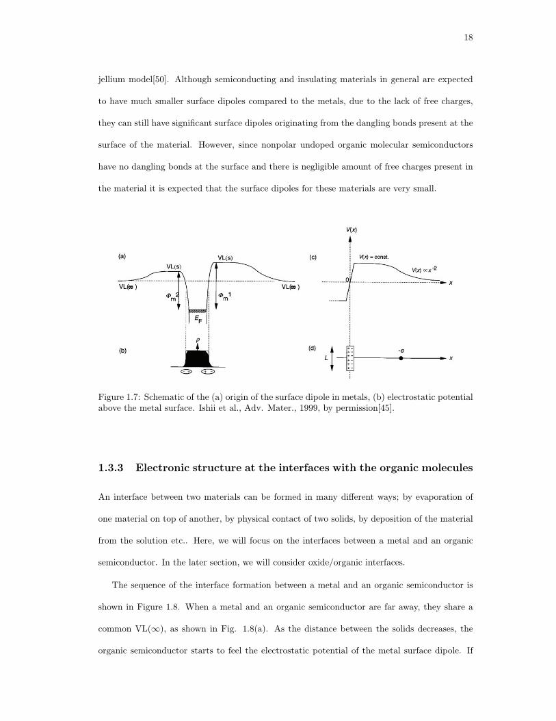
18
jellium model[50]. Although semiconducting and insulating materials in general are expected
to have much smaller surface dipoles compared to the metals, due to the lack of free charges,
they can still have significant surface dipoles originating from the dangling bonds present at the
surface of the material. However, since nonpolar undoped organic molecular semiconductors
have no dangling bonds at the surface and there is negligible amount of free charges present in
the material it is expected that the surface dipoles for these materials are very small.
Figure 1.7: Schematic of the (a) origin of the surface dipole in metals, (b) electrostatic potentialabove the metal surface. Ishii et al., Adv. Mater., 1999, by permission[45].
1.3.3 Electronic structure at the interfaces with the organic molecules
An interface between two materials can be formed in many different ways; by evaporation of
one material on top of another, by physical contact of two solids, by deposition of the material
from the solution etc.. Here, we will focus on the interfaces between a metal and an organic
semiconductor. In the later section, we will consider oxide/organic interfaces.
The sequence of the interface formation between a metal and an organic semiconductor is
shown in Figure 1.8. When a metal and an organic semiconductor are far away, they share a
common VL(∞), as shown in Fig. 1.8(a). As the distance between the solids decreases, the
organic semiconductor starts to feel the electrostatic potential of the metal surface dipole. If
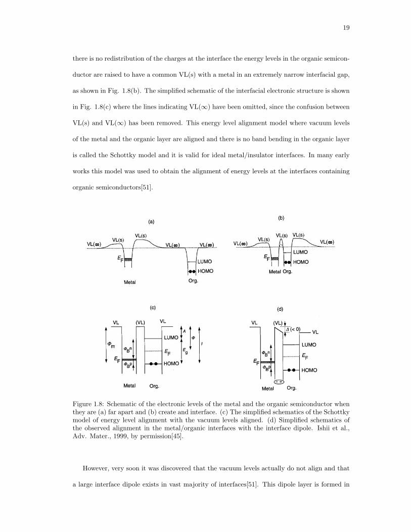
19
there is no redistribution of the charges at the interface the energy levels in the organic semicon-
ductor are raised to have a common VL(s) with a metal in an extremely narrow interfacial gap,
as shown in Fig. 1.8(b). The simplified schematic of the interfacial electronic structure is shown
in Fig. 1.8(c) where the lines indicating VL(∞) have been omitted, since the confusion between
VL(s) and VL(∞) has been removed. This energy level alignment model where vacuum levels
of the metal and the organic layer are aligned and there is no band bending in the organic layer
is called the Schottky model and it is valid for ideal metal/insulator interfaces. In many early
works this model was used to obtain the alignment of energy levels at the interfaces containing
organic semiconductors[51].
Figure 1.8: Schematic of the electronic levels of the metal and the organic semiconductor whenthey are (a) far apart and (b) create and interface. (c) The simplified schematics of the Schottkymodel of energy level alignment with the vacuum levels aligned. (d) Simplified schematics ofthe observed alignment in the metal/organic interfaces with the interface dipole. Ishii et al.,Adv. Mater., 1999, by permission[45].
However, very soon it was discovered that the vacuum levels actually do not align and that
a large interface dipole exists in vast majority of interfaces[51]. This dipole layer is formed in

20
addition to the surface dipole of a clean metal surface discussed before. There are many origins
of the interface dipole layer, such as charge transfer across the interface, redistribution of the
electron density at the metal surface due to the presence of the organic layer, interfacial chemical
reaction and other types of charge rearrangement. With such an interfacial dipole formed, there
will be an abrupt shift in the potential at the interface leading to a shift of the VL by ∆, as
shown in Fig. 1.8(d). Furthermore, all electronic states in the organic semiconductor molecule
will shift by the same amount ∆ as well as the vacuum level (VL) on the organic semiconductor
side of the interface.
Nielsen pointed out the importance of the interfacial dipole layer in 1975[52], but not much
experimental work was carried out at the time. In the field of the organic devices, when the
electronic properties of the metal/organic interfaces just started to be studied, the existence
of the interfacial dipole has often been neglected. In contrast, in the field of surface science,
the energy shift of the vacuum level upon molecular adsorption on the surfaces has been a well
known issue. Usually, this phenomenon is called the change in the work function of the metal
and extensive studies have been carried out for the small molecules[53]. Following the custom
in the field of surface science, we will take ∆ to be positive when VL is raised by deposition,
and vice versa, it will be considered negative if the VL is lowered.
If the organic semiconductor deposited on the metal surface is thick, band bending should
also be considered and can introduce additional changes the electronic states of the organic
semiconductor. Band bending concept is well known in the interfaces with the inorganic semi-
conductors and has to some degree been explored for the organic materials. If we assume that
the organic semiconductor is undoped and the amount of free charges is negligible, the Fermi
level will be in the middle of the HOMO-LUMO gap of the organic material. In general, work
functions, i.e. the energy separation between the vacuum level and the Fermi level, for the
metal and organic semiconductor are different. Similarly to the inorganic semiconductors, if
the number of the available mobile carriers in the organic layer is sufficiently large, there will
be charge redistribution around the interface to account for the work function difference. If
21
the work function of the metal is larger than that of the organic layer, some electrons may be
transferred from the organic semiconductor to the metal leading to the negative and positive
charging of the metal and the organic layer, respectively. This flow continues until the Fermi
levels are aligned between the metal and the bulk of the organic layer. The region in the organic
layer from which the electrons are transferred is called the depletion region. The band bending
model of energy level alignment at the interfaces with the organic molecules is shown in Fig.
1.9(a) and (b). The energy level alignment model in which there is no interfacial dipole, but
there is band bending (Fig. 1.9)(a)) is called Schottky-Mott model and it previously had a
great success describing the metal/inorganic semiconductor interfaces. However, for organic
molecules, an additional interface dipole might be expected, as shown in Fig. 1.9(b). As men-
tioned earlier, such alignment of the Fermi level by band bending is possible only when sufficient
number of mobile charge carriers are available, either in a thick organic layer or an organic layer
with a good semiconducting character. In these cases we can estimate the depletion region
width by using the equation for the inorganic/metal interfaces[54]. Assuming the charge carrier
density of ∼1014 cm−3[55] in the undoped organic semiconductors, the relative permittivity of
ϵ ∼ 3[56] and built-in potential of ∼1 V, we get the depletion region width to be ∼1 µm that
is comparable to a typical depletion width of ∼10 µm found in the inorganic semiconductors.
For very thin layers nearly flat-band situation at the interface is expected, as shown in
Fig. 1.8(d) and the alignment of the Fermi level is not easily established. Thus in case of the
systems in our study, either monolayers of chemisorbed dye or a few nanometers thick organic
layer, we can assume almost flat-band situation, as shown in Fig. 1.8(d) as a very good first
approximation.
1.3.4 Interfaces between the organic molecules and the oxides
The interest in the oxide/organic interfaces started in the 1990s when it was discovered that an
oxide layer added in between the metal anode and the organic film in the organic light-emitting
diodes can decrease the hole-injection barrier[57]. This discovery resulted in decrease in the
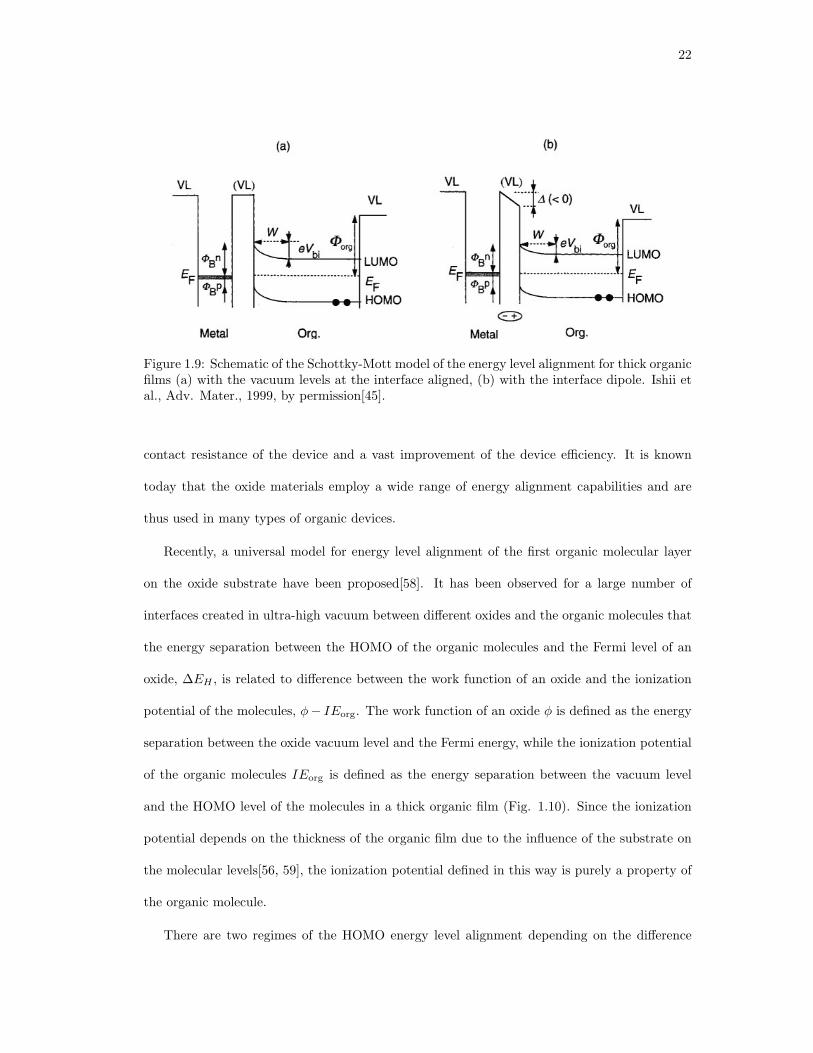
22
Figure 1.9: Schematic of the Schottky-Mott model of the energy level alignment for thick organicfilms (a) with the vacuum levels at the interface aligned, (b) with the interface dipole. Ishii etal., Adv. Mater., 1999, by permission[45].
contact resistance of the device and a vast improvement of the device efficiency. It is known
today that the oxide materials employ a wide range of energy alignment capabilities and are
thus used in many types of organic devices.
Recently, a universal model for energy level alignment of the first organic molecular layer
on the oxide substrate have been proposed[58]. It has been observed for a large number of
interfaces created in ultra-high vacuum between different oxides and the organic molecules that
the energy separation between the HOMO of the organic molecules and the Fermi level of an
oxide, ∆EH , is related to difference between the work function of an oxide and the ionization
potential of the molecules, ϕ− IEorg. The work function of an oxide ϕ is defined as the energy
separation between the oxide vacuum level and the Fermi energy, while the ionization potential
of the organic molecules IEorg is defined as the energy separation between the vacuum level
and the HOMO level of the molecules in a thick organic film (Fig. 1.10). Since the ionization
potential depends on the thickness of the organic film due to the influence of the substrate on
the molecular levels[56, 59], the ionization potential defined in this way is purely a property of
the organic molecule.
There are two regimes of the HOMO energy level alignment depending on the difference

23
CB
VB
VLoxide
VLorg
EF
φ
IEorg
∆EH
oxide
organic
semiconductor
Figure 1.10: Schematic of the important energy alignment parameters for the metal oxide andthe organic semiconductor. CB and VB denote conduction and valence band respectively.
between the oxide work function and the organic ionization potential. If ϕ− IEorg < 0 eV, the
energy separation between the HOMO and the Fermi energy is given by
∆EH = (IEorg − ϕ) + 0.3 eV. (1.2)
In this range HOMO position changes linearly with the oxide work function. If ϕ−IEorg > 0 eV
the HOMO position is independent of the oxide work function and it is pinned at 0.3 eV below
the Fermi level.
This trend shows a distinct change in the energy level alignment regime when the work
function of the oxide becomes equal to the ionization potential of the molecule. Once the work
function of the substrate has exceeded the ionization potential of the adsorbed molecule, ∆EH
establishes a minimum value, and remains constant with further increases in work function of
the oxide.
This behavior of the HOMO energy level alignment is, in a simple picture, explained by
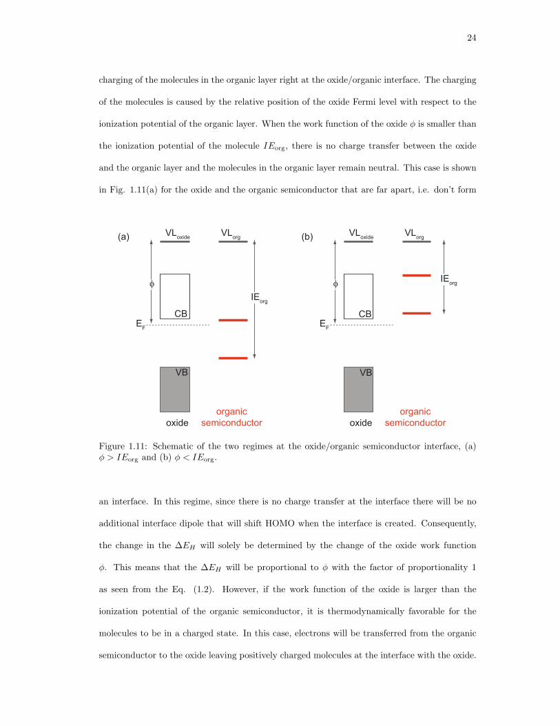
24
charging of the molecules in the organic layer right at the oxide/organic interface. The charging
of the molecules is caused by the relative position of the oxide Fermi level with respect to the
ionization potential of the organic layer. When the work function of the oxide ϕ is smaller than
the ionization potential of the molecule IEorg, there is no charge transfer between the oxide
and the organic layer and the molecules in the organic layer remain neutral. This case is shown
in Fig. 1.11(a) for the oxide and the organic semiconductor that are far apart, i.e. don’t form
CB
VB
VLoxide
VLorg
EF
φ
IEorg
oxide
organic
semiconductor
(a)
CB
VB
VLoxide
VLorg
EF
φIE
org
oxide
organic
semiconductor
(b)
Figure 1.11: Schematic of the two regimes at the oxide/organic semiconductor interface, (a)ϕ > IEorg and (b) ϕ < IEorg.
an interface. In this regime, since there is no charge transfer at the interface there will be no
additional interface dipole that will shift HOMO when the interface is created. Consequently,
the change in the ∆EH will solely be determined by the change of the oxide work function
ϕ. This means that the ∆EH will be proportional to ϕ with the factor of proportionality 1
as seen from the Eq. (1.2). However, if the work function of the oxide is larger than the
ionization potential of the organic semiconductor, it is thermodynamically favorable for the
molecules to be in a charged state. In this case, electrons will be transferred from the organic
semiconductor to the oxide leaving positively charged molecules at the interface with the oxide.
25
This case is shown in Fig. 1.11(b). In this regime, as the work function of the oxide increases,
the concentration of ionized molecules increases as well, effectively creating the interface dipole
that is proportional to the change in the work function. Consequently, the energy separation
between HOMO and Fermi energy remains constant with the increase in the oxide work function.
This case corresponds to the Fermi-level pinning regime.
The models of the energy level alignment presented so far will be compared to the energy
level alignment measured in this thesis to see whether they hold up to experimental verification.
1.4 Thesis Outline
In this thesis we are focused on gaining a comprehensive understanding of the electronic struc-
ture, adsorption geometry and the energy level alignment at interfaces between tetraphenylpor-
phyrin (TPP)-derived molecules and metal oxide, as well as metal surfaces. In our study we
used several surface science techniques: ultraviolet, X-ray and inverse photoemission spectro-
scopies (UPS, XPS and IPS), near edge X-ray absorption fine structure (NEXAFS), reflection
electron energy loss spectroscopy (REELS) and scanning tunneling microscopy (STM) in ultra-
high vacuum environment and UV-visible absorption spectroscopy that is not a surface sensitive
technique performed in ambient conditions. We also performed quantum chemistry calculations
and compared theoretically obtained electronic structure to our experimental UPS and IPS
spectra. In Chapter 2 all of the mentioned techniques will be explained and the experimental
setups for each of them will be presented. All measurements will be presented in Chapters 3, 4
and 5. In Chapter 3 we present a study of the adsorption geometry and the electronic structure,
as well as the energy level alignment of four different TPP-derived dye molecules chemisorbed
on TiO2(110) and ZnO(1120) single crystal surfaces. Specifically, we focused on the influence
of the molecule-molecule interaction and the type of the functional group on the phenyl rings
on the electronic structure of the adsorbed molecule. In Chapter 4 we present the influence of
different adsorption geometries and central metal ion on the electronic structure and the en-
ergy level alignment at the interface between free-base and zinc TPP-derived dye molecules and

26
ZnO(1120) single crystal surface. In Chapter 5 we present the influence of different substrates
on the electronic structure, energy level alignment and the adsorption geometry of the evapo-
rated zinc tetraphenylporphyrin (ZnTPP) thin films on Ag(100) and TiO2(110) surfaces. We
also studied the changes induced in both the electronic structure of the adsorbed molecules and
the electronic excitations upon changes in the film thickness. The results of these chapters will
be compared to the ones presently found in literature and to the models described in previous
sections.
27
Chapter 2
Experimental and theoretical methods
2.1 Introduction
There are two main parts of this thesis. In the first part the binding geometry and the electronic
structure of the organic dye molecules chemisorbed on single crystal metal oxide surfaces has
been studied. The second part concerns with the binding geometry and energy level alignment
at the interfaces between the organic molecules and single crystal metal surfaces.
To be able to study intrinsic properties of the aforementioned interfaces, atomically clean
well-ordered surfaces are mandated. This implies the use of ultra high vacuum (UHV) environ-
ments during preparation procedures and measurements performed on the sample.
Also, to be able to access the electronic and geometric properties of the adsorbed organic
molecules, a monolayer, or several layers, of molecules have been deposited on different sub-
strates of interest and studied with surface sensitive techniques. These standard surface science
techniques are sensitive to the first few atomic layers of the material and thus are very useful
in our study of interfacial properties. Ultraviolet photoemission spectroscopy (UPS) and in-
verse photoemission spectroscopy (IPS) are used to study occupied and unoccupied electronic
states of the adsorbed molecules. The excited states of the electrons in the adsorbed molecular
layer have been studied with reflection electron energy loss spectroscopy (REELS). Since the
excitations in REELS are closely related to the optical transitions, such measurement gave us
opportunity to study optical properties of the adsorbed layer under UHV conditions. Scanning
tunneling microscopy (STM) and near-edge X-ray absorption spectroscopy (NEXAFS) are pri-
marily used to study the adsorption geometry of the molecules. Another technique, UV-visible
28
absorption spectroscopy, that is not a surface sensitive technique and has not been done in
UHV, was used primarily to identify synthesized dye molecules.
UPS, IPS, REELS and STM measurements were performed in two separate UHV chambers
at Rutgers University with base pressure of ≈ 5 · 10−10 Torr. NEXAFS measurements were
done at the beamline U7a at the National Synchrotron Light Source (NSLS) at Brookhaven
National Laboratory and UV-visible absorption spectroscopy measurements were done by our
collaborators at the Chemistry Department at Rutgers University, Newark.
The main characteristics of the ultra high vacuum environment and how it can be achieved
in the lab will be described in this chapter as well as the details of aforementioned experimental
techniques.
2.2 Ultra High Vacuum (UHV)
As we have already mentioned, to avoid surface contamination of the of the samples with the
contaminants usually found in ambient conditions, it is necessary to do the preparation and all
the measurements in the ultra high vacuum (UHV) environment.
The main source of surface contamination is the air surrounding the sample. Some compo-
nents of air, like oxygen and water molecules and other contaminants collide with the surface
of the sample and get either chemisorbed or physisorbed on it. In the vacuum environments
the number of particles, and thus the probability of collision and adsorption to the surface is
greatly reduced. For example, it can be estimated that at atmosphere pressure (760 Torr), if
one considers the sticking probability of the contaminants to the surface to be 1, a monolayer of
contaminants (∼ 1015 particles per cm2) will be formed within nanoseconds. As a consequence,
a vacuum pressure that is about 10−13 of an atmosphere or better is needed to keep the sample
surface clean for a few hours while performing different measurements.
According to the range of pressures, vacuum environments are roughly divided into five
categories, as shown in the Table 2.1.
An ultra high vacuum (UHV) environment falls in the pressure range of 10−9 to 10−12 Torr

29
Table 2.1: Vacuum types and corresponding pressure ranges
Vacuum type Pressure range (Torr)
Low vacuum 760 - 25
Medium vacuum 25 - 10−3
High vacuum 10−3 - 10−9
Ultra high vacuum 10−9 - 10−12
Extremely high vacuum < 10−12
which is, for the comparison, approximately the pressure of the Moon’s atmosphere. Such low
pressure environments can be created in the lab inside of a sealed stainless steel chamber using
several pumping stages.
B
body of the pump
Ti cathodes
anode
(b)(a) (c)
e-
1
2 3
Figure 2.1: (a) A cross section of the rotary vane pump. Vanes (3) are mounted on the rotor(2) that rotates inside of a cylindrical cavity (1) that is a part of the pump’s body; (b) Bladeson rotors and stators in a turbomolecular pump; (c) A cross section of a pumping cell in an ionpump.
As the first stage, a rotary vane pump is used to bring down the pressure in the chamber
from atmospheric pressure. Figure 2.1(a) schematically shows the cross section of the rotary
vane pump body. The pump consists of vanes mounted on a rotor that rotates inside of a
cylindrical cavity with the inlet and the outlet of the pump. The axes of rotor and cylindrical
cavity are offset, which causes eccentricity. Vanes on the rotor can slide towards the walls of
cylindrical cavity and create effective seal between the inlet and the outlet of the pump, that
are on lower and higher pressure respectively. As the vanes rotate, gas molecules enter through
the inlet and are pushed out to the outlet. When the pressure of ∼ 100 mTorr is achieved in

30
the chamber a turbomolecular pump can be turned on.
The turbomolecular pump consists of several pairs of rotating angled blades and stationary
blades, called rotors and stators respectively, shown in Fig. 2.1(b). As the gas molecules enter
the pump’s inlet, rotor in the first level gives them additional momentum towards the pump’s
outlet. Molecules then pass through the holes in the stator to the rotor blades in the next level.
In this manner, gas is pushed and compressed at the outlet of the pump where it’s pumped
away by the rotary vane pump. The rotary vane pump maintains the outlet pressure of the
turbomolecular pump at the level of several mTorr. The rotors and stators of the turbomolecular
pump get successively closer to one another in each level and the tilt angle of the blades is
increasing, resulting in compression factor of about 5 per level. This amounts to the ratio of
∼ 106 between the pressures at the outlet and inlet of the turbomolecular pump.
When the pressure in the chamber is below ∼ 10−6 Torr, an ion pump can be turned on.
The ion pump ionizes and captures residual gas molecules and further decreases the pressure in
the chamber. It consists of the collection of cells, the one of which is shown in Fig. 2.1(c). Each
cell consists of two parallel stainless steel walls coated with Ti film and an array of stainless steel
cylinders whose axes are perpendicular to the walls. High voltage (∼ 6 kV) is applied between
the walls and the cylinders, that act as a cathode and an anode, respectively. Furthermore,
magnetic field of about 1500 G is applied along the axes of the cylinders. Presence of high
electric field causes electrons to be emitted from the Ti coated walls while presence of magnetic
field is restricting their motion to a helical path along cylinder’s axis. The emitted electrons
hit residual gas molecules and ionize them. Positive ions are, due to high voltage, accelerated
toward Ti coated walls where they are embedded or chemisorbed. The impact of ions causes
some Ti atoms to sublimate, which coats the surface of an anode and traps more molecules.
After the ion pump is turned on, the pressure in the chamber can reach ∼ 10−8 Torr in several
hours, but it won’t decrease much further because of the residual water vapor in the chamber.
To desorb water molecules from the chamber walls, the chamber needs to be heated above 100C
for about 24 hours. After cooling, the pressure in the chamber will be ≤ 5 · 10−10 Torr, which

31
is suitable for measurements.
2.3 Photoemission Spectroscopy
Photoemission spectroscopy is based on the photoelectric effect and is used to study the occupied
electronic states of a sample. The measurement is performed by directing a monoenergetic
photon beam onto a sample and collecting electrons that are emitted. In X-ray photoemission
spectroscopy (XPS) photons with energies on the order of 1 keV are used to primarily probe
occupied electronic core levels of the system. Ultraviolet photoemission spectroscopy (UPS), on
the other hand, uses photons with energy of few tens of eV to probe occupied states of smaller
binding energies, that is, the valence states of the system. It is important to note that XPS
probes the valence states as well, but the photoabsorption cross section for these states is much
smaller in XPS compared to UPS. UPS is, thus, the technique of choice for probing the valence
states since it offers greater sensitivity in this energy region.
2.3.1 The photoemission process
The photoemission process for electrons with two different initial electron energies in the metal
sample is shown in Figure 2.2. A photon of energy hν is absorbed by an electron with initial
energy Ei within the metal and excited to the final state with energy Ef . If the final energy
of the electron is above a vacuum level (Evac), it can escape the sample. If the electron is
not inelastically scattered on its way out of the sample, information about its initial state is
contained in its kinetic energy after it leaves the sample. The electron inelastic mean free
path (IMFP), an average distance that an electron can travel in a solid before it inelastically
scatters, thus determines the surface sensitivity of photoemission spectroscopy, as well as all
electron spectroscopies.
The electron IMFP depends on the initial kinetic energy of electron and on the material with
which the electron interacts. However, the kinetic energy dependence of the IMFP for many
different elemental solids is very similar and follows a so-called “universal curve”[53], shown in
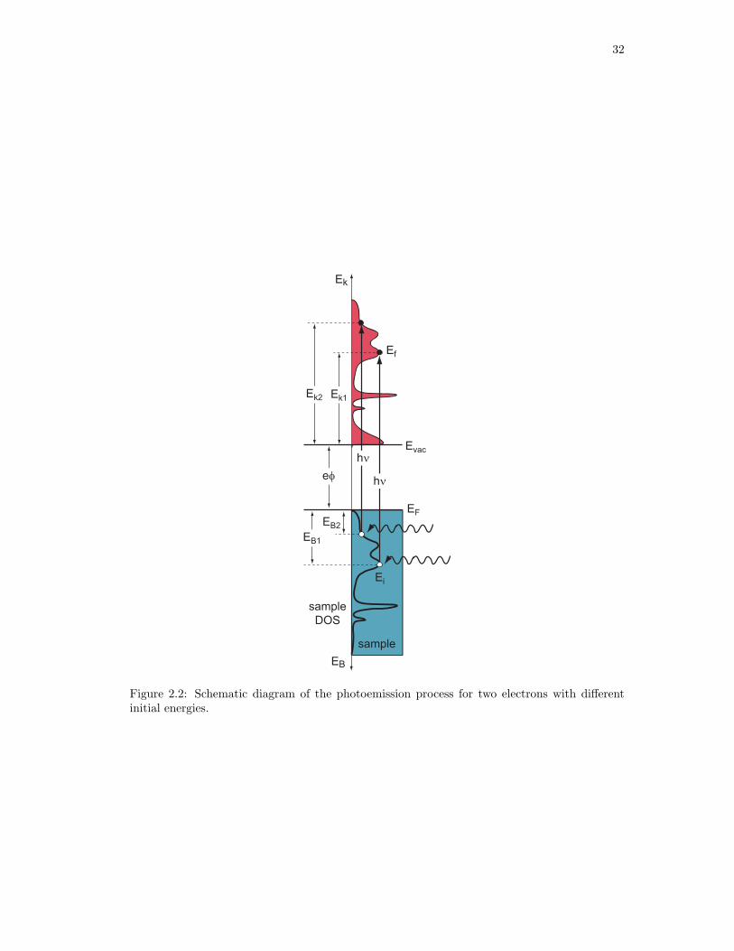
32
Ek
sample
DOS
hν
EB
Evac
sample
hν
EF
Ei
Ef
Ek1Ek2
EB2EB1
eφ
Figure 2.2: Schematic diagram of the photoemission process for two electrons with differentinitial energies.
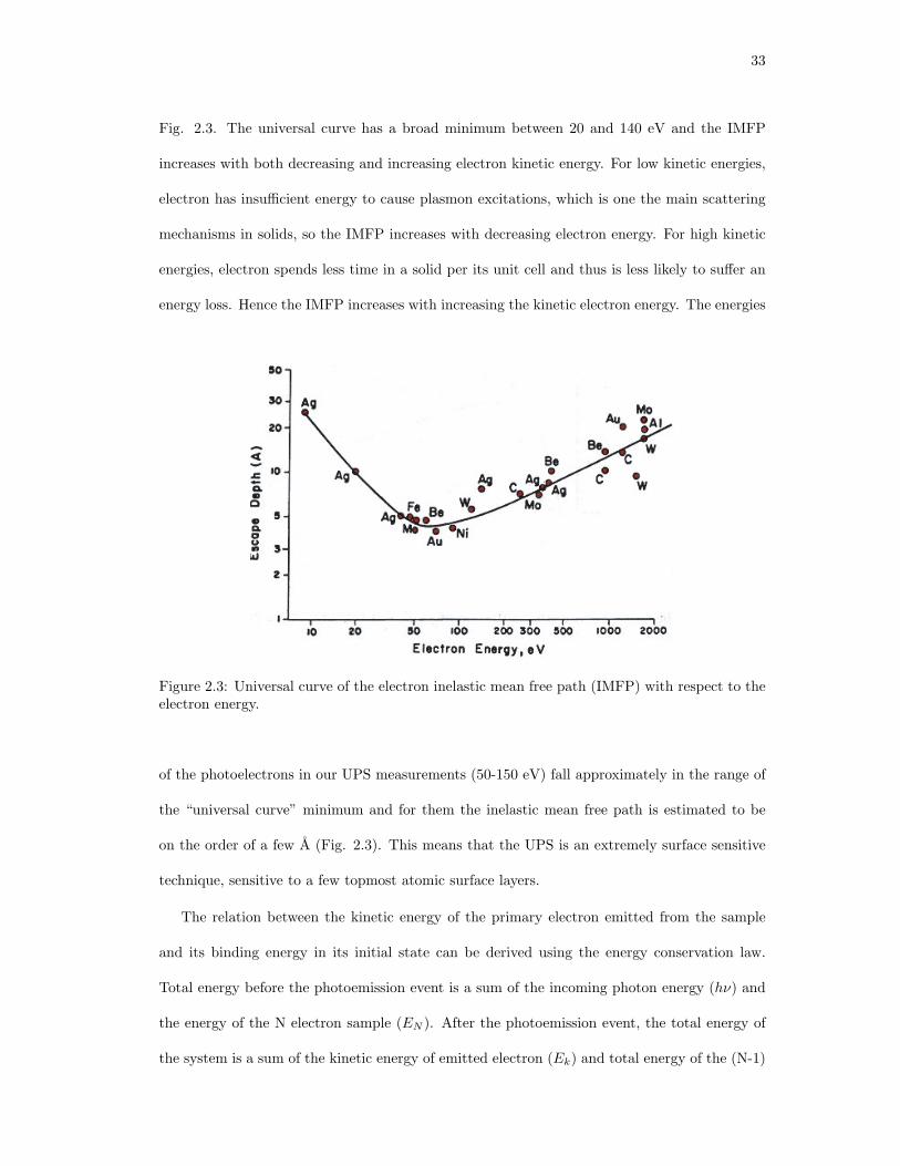
33
Fig. 2.3. The universal curve has a broad minimum between 20 and 140 eV and the IMFP
increases with both decreasing and increasing electron kinetic energy. For low kinetic energies,
electron has insufficient energy to cause plasmon excitations, which is one the main scattering
mechanisms in solids, so the IMFP increases with decreasing electron energy. For high kinetic
energies, electron spends less time in a solid per its unit cell and thus is less likely to suffer an
energy loss. Hence the IMFP increases with increasing the kinetic electron energy. The energies
Figure 2.3: Universal curve of the electron inelastic mean free path (IMFP) with respect to theelectron energy.
of the photoelectrons in our UPS measurements (50-150 eV) fall approximately in the range of
the “universal curve” minimum and for them the inelastic mean free path is estimated to be
on the order of a few A (Fig. 2.3). This means that the UPS is an extremely surface sensitive
technique, sensitive to a few topmost atomic surface layers.
The relation between the kinetic energy of the primary electron emitted from the sample
and its binding energy in its initial state can be derived using the energy conservation law.
Total energy before the photoemission event is a sum of the incoming photon energy (hν) and
the energy of the N electron sample (EN ). After the photoemission event, the total energy of
the system is a sum of the kinetic energy of emitted electron (Ek) and total energy of the (N-1)
34
electron sample (EN−1). Equating these two energies, we get the expression for the kinetic
energy of the photoelectron as
Ek = hν + (EN − EN−1). (2.1)
The term in parenthesis (EN −EN−1) is defined as the binding energy EB of the initial electron
state with respect to the vacuum level and it is a negative quantity.
Very often, it is more convenient to reference binding energy with respect to the Fermi
energy of the sample, instead of vacuum level, since the Fermi, not the vacuum level, will be
common for all the materials in the thermal equilibrium with the sample. The equation for the
kinetic energy of the photoelectron is then given as
Ek = hν + EB − eϕ, (2.2)
where ϕ is a work function of a sample. However, defining a Fermi level for an oxide, the
material most extensively used in our studies, is problematic since there are no states at the
Fermi level and, thus, no states to represent the Fermi level in the photoemission spectrum.
This issue is further discussed in Appendix A. Binding (EB) and kinetic (Ek) energies defined
in this way are denoted for two photoelectrons in Fig. 2.2. Work function of the metal sample
(ϕ) is also denoted on the figure.
For the resulting binding energies from the UPS spectra the validity of Koopmans’ theorem
is assumed. Koopmans’ theorem states that the first ionization energy of the system is equal
to the negative of the binding energy of the highest occupied orbital of the system[60]. This
theorem is exact in the framework of Hartree-Fock approximation[61] where the relaxation
effects of the electron density remaining in the system after one electron removal are neglected.
This means that the wave functions describing the many-body system before and after the
electron removal are assumed to be the same. This contribution of the orbital relaxation to
the total energy is called relaxation energy (Erelax). Furthermore, in this approximation a
part of the electron-electron interaction energy, called the electron correlation energy (Ecorr) is
neglected. This contribution corresponds to the electrostatic, or Coulomb correlation between
35
two electrons in the system. Another part of the electron-electron interaction energy, called
the exchange interaction energy (Eexch), that takes into account the spins of the electrons is
included in the total energy in Hartree-Fock approximation.
In real materials, however, neither correlation nor relaxation effects can be neglected and
thus the Hartree-Fock approximation is not valid, but in many cases Koopamans’ theorem gives
good results for the ionization potentials. The reason for that is that these two energy terms
are approximately of the same magnitude, but have opposite signs (Ecorr ≈ −Erelax) so they
cancel. In case of the materials studied in this thesis, Koopmans’ theorem gives good results for
the ionization potentials. In general, however, Koopmans’ theorem should be used with care.
2.3.2 Photoabsorption cross section
The photoemission spectrum represents the number of photoelectrons collected as a function
of photoelectron kinetic energy, integrated over all photoelectron k vector directions. The
spectrum I(E) is proportional to the density of occupied electronic states N(E) times the
photoabsorption cross section σabs at a particular photoelectron energy E. Thus, to find the
density of occupied states, one needs to, in principle, know σabs and deconvolve it from the
measured photoemission spectrum.
The photoemission cross section can be derived using the expression for the transition rate
or the probability of photon absorption per unit time, known as Fermi’s Golden Rule
Γ =2π
~|⟨Ψf |H ′|Ψi⟩|2ρf (Ei + hν), (2.3)
where Ψi and Ψf are initial and final state wave functions of an electron, ρf (Ei + hν) is the
density of final states at the energy of the final state Ef = Ei + hν and H ′ is the part of the
the Hamiltonian describing the interaction between the electron and the electromagnetic field
of a photon. To simplify the calculation we can choose a so-called transverse gauge (ϕ = 0 and
∇ ·A = 0) and keeping only linear term of the vector potential A, interaction Hamiltonian H ′
is H ′ = −e/mc(A · p) where e is the charge and m is the mass of an electron and p is the
electron momentum operator.

36
The spatial dependence of the vector potential is given by exp(−ik ·r). Since the wavelength
of the incident photon is large compared to the atom spacing in the sample, this exponential
function can be approximated by 1. This approximation is know as the dipole approximation.
The photoabsorption rate is in the dipole approximation given by
Γ =2π
~
( e
mc
)2
|ϵ · ⟨Ψf |p|Ψi⟩|2ρf (Ei + hν) (2.4)
The photoabsorption differential cross section can be obtained by dividing Eq. (2.4) by the
incoming photon flux and explicitly expressing ρf as the free electron density of states[62]
dσabs
dΩ=
α
2π
k
m
1
hν|ϵ · ⟨Ψf |p|Ψi⟩|2, (2.5)
where α = e2/mc = 1/137 is the fine structure constant, k is the magnitude of the wavevector
of an electron in the final state and ϵ is the unit vector in the direction of the electric field of
the photon.
Furthermore, it is important to note that the momentum operator p in the matrix element
of the photoabsorption cross section in Eq. (2.5) can be rewritten in terms of the position
operator r using the [r,H] commutator as
p =−im
~[r,H], (2.6)
where m is the mass and H is the Hamiltonian operator. The matrix element from the Eq.
(2.5), which we will denote with M, is then given by
M =−im
~⟨Ψf |[r, H]|Ψi⟩ =
im
~(Ef − Ei)⟨Ψf |r|Ψi⟩, (2.7)
where Ef and Ei are the eigenvalues of the Hamiltonian in the basis of states Ψf and Ψi. This
matrix element is commonly known as the transition dipole moment.
Finally, using the dipole operator µ = er, the transition dipole moment can be written as
M =im
e~(Ef − Ei)⟨Ψf |µ|Ψi⟩. (2.8)
The absorption cross section has been calculated as a function of incident photon energy for
37
electronic states of many materials. Observing the energy dependence of the cross section of a
spectral feature is often a useful way to identify its orbital character.
2.3.3 Ultraviolet photoemission spectroscopy (UPS) instrumentation
In ultraviolet photoemission spectroscopy (UPS) UV photons are used to excite electrons bound
in the sample. The source of monochromatic UV light in our UPS measurements was a He
discharge lamp. In this UV source, ultra-high purity He gas is introduced between two high
voltage electrodes and an electrical arc between them is used to excite electrons in He atoms.
As electrons decay back to their ground states, they emit photons that are guided to the sample
using a thin glass capillary. Two strong emission lines created in the discharge are used for UPS.
One is He I line, at 21.2 eV, that corresponds to the photons being emitted as the electrons
in neutral He atoms decay from 2p to 1s state. He IIα line, at 40.8 eV, corresponds to the
transition between the same states, but in the singly ionized He atoms. The ratio between He II
and He I lines increases rapidly with decreasing the He gas pressure in the source. The energy
widths of these emission lines are smaller than 0.1 eV[63].
Photoelectrons emitted from the sample are collected and analyzed using a double-pass
cylindrical mirror analyzer (CMA). The cross section along the symmetry axis of CMA is
schematically shown in Fig. 2.4. Cylindrical mirror analyzer consists of two cylindrical elec-
trodes called inner and outer cylinders. Inner cylinder has slits through which electrons can
pass, while outer cylinder is continuous. If a voltage is applied between the cylinders, incoming
electron trajectories inside of CMA will be deflected with a radius that depends on the electron
kinetic energy. By setting a specific set of voltages between these two cylinders, only electrons
that have kinetic energy in some energy range will be able to pass through the slits in the inner
cylinder and through the apertures, and finally reach the “channeltron” electron multiplier. All
other electrons, with either higher or lower kinetic energies, will hit the walls of CMA and be
absorbed. By increasing kinetic energy at which photoelectrons are collected in stepwise fashion
and counting the number of photoelectrons at each kinetic energy a photoemission spectrum is

38
obtained. In general, commercial CMAs are double-pass, where the second stage of filtering is
aperture
controller
channeltron
electron
multiplierpath of
an electron
electron
gun sample
outer
cylinder
inner
cylinder
spherical
grids
aperture #2
aperture #1
Figure 2.4: Schematic diagram of a double-pass cylindrical mirror analyzer (CMA).
added to reduce spurious background signals due to the secondary electrons generated within
the analyzer. In double-pass CMAs electrons travel in a “half of figure-of-eight” path (Fig. 2.4).
If an electron passes through the top slits in the inner cylinder in the first stage of CMA and
then through the aperture, in the second stage it will pass through the bottom slits in the inner
cylinder, as shown in Fig. 2.4. On their path from the analyzer entrance to the channeltron
electron multiplier, electrons pass through two apertures, denoted by aperture #1 and aperture
#2 in Fig. 2.4. One aperture is located between two CMA stages and the other one at the
channeltron entrance. The diameter of these apertures can be changed externally between two
sizes. The aperture size affects the energy resolution and the number of detected electrons in
opposite ways. A smaller diameter aperture will give higher energy resolution, but at the cost
of lower count rate at the detector.
For our UPS measurements, the CMA is operated in a so-called retarding mode with both

39
apertures set at a large diameter setting, which is about 1 mm. In this mode, the first of the two
spherical grids, shown in the Fig. 2.4, is grounded to keep the space between the sample and
the analyzer free of any electric fields. The second grid is, however, set to a negative voltage.
This negative voltage reduces the kinetic energy of the incoming photoelectrons so that all the
photoelectrons entering the channeltron have the same energy, known as the pass energy. Only
electrons in a narrow range around a specific kinetic energy will be reduced to the pass energy
and reach the detector. The same as discussed above, the cylinder voltages are ramped to detect
electrons at a certain kinetic energy and obtain the photoelectron spectrum.
The channeltron electron multiplier is positioned at the end of the CMA and it is used to
collect electrons that passed through the CMA, amplify the current signal created by electrons
and transform it to a voltage signal. This voltage signal is further amplified and shaped by
external electronics and finally read by a computer. The channeltron consist of a conically
shaped cup with a curved tube extending off from it. The inner surface of the channeltron (Fig.
2.5) is coated with a layer of SiO2 on top of the conductive layer. As an incoming electron
-+
e-
input
current
output
voltage
Figure 2.5: Schematic diagram of a channeltron electron multiplier and the current to voltageconversion circuit.
strikes the wall of the conical cup, due to the secondary emission process, on average several
new electrons are created. These electrons are guided and accelerated by the positive voltage
40
applied at the end of the curved tube, they again hit the walls of channeltron and create more
electrons. This avalanche process ensures that there is a large number of electrons at the end
of the tube (107) that enter the current to voltage conversion circuit. The voltage pulse is
easily detected and shaped with the standard amplifying electronics and allows counting of
primary electrons that are transmitted through the analyzer and have reached the channeltron.
Amplified voltage pulses are read and counted during some preset period of time at different
electron kinetic energies by a computer and displayed as a photoemission spectrum.
The resolving power of the energy analyzer is given by E/∆E, where E is the energy of the
electrons reaching the detector, in our case the pass energy (E0), and ∆E is the energy range
of the photoelectrons reaching the detector. Since the resolving power of the analyzer is set by
its geometry (E/∆E = const.), the energy range of photoelectrons reaching the detector will
be proportional to the pass energy (∆E ∝ E0). If the pass energy is, thus decreased the energy
range of the electrons reaching the detector will decrease as well, which increases the resolution
of the analyzer. The majority of the UPS measurements presented in this thesis were done with
a set pass energy of 15 eV, for which the energy resolution was around 0.5 eV1. Decreasing the
pass energy will also decrease the count rate, which increases the collection time to obtain a
good signal to noise ratio.
The energies in the photoemission spectrum obtained in the described way are the kinetic
energies of the photoelectrons measured with respect to the vacuum level of the analyzer, that
is in principle unknown. To be able to further interpret the obtained photoemission spectrum,
the energy scale needs to be calibrated to the Fermi energy of the sample as the reference
energy. The UPS energy scale calibration procedure, in particular for the metal oxide samples,
is described in detail in Appendix A.
To obtain a full energy level alignment diagram at the interfaces between the adsorbed
molecules and metal or metal oxide substrates, work functions and ionization potentials of the
1The energy resolution of CMA in our measurements was determined by measuring the width of the Fermiedge of gold sample in UPS during a calibration process described in Appendinx A
41
interface constituents need to obtained. Such measurements are especially important for the
evaluation of the interface dipoles created upon molecule adsorption. Besides studying the
occupied valence states, UPS can also be used to obtain the work function and the ionization
potential of the sample. This type of measurement is also described in Appendix A.
2.4 Inverse Photoemission Spectroscopy
Inverse photoemission spectroscopy (IPS) is a technique complementary to the photoemission
spectroscopy as it is used to study the unoccupied states of a sample. For this type of spec-
troscopy, a highly collimated beam of electrons with a well defined energy is directed towards
the sample and couples to the high lying unoccupied states of the sample above the vacuum
level. A portion of incoming electrons will then decay to the lower lying unoccupied states by
emitting a photon. The energy of the emitted photon is given by a difference between the initial
and final state energies of an electron. This process is illustrated for one electron in Fig. 2.6.
Since the initial energy of the electron is known, by collecting and measuring the energy of the
emerging photons, the energy of the final state of the electron can be obtained. By measuring
the number of photons emitted from the sample at each photon energy, information about the
unoccupied states of the sample can be deduced. Inverse photoemission spectroscopy is also a
surface sensitive technique. For example, for the electron beam with the energy of around 20
eV, that we most often use in our experiments, the IMFP is found to be a few A (Fig. 2.3).
2.4.1 Inverse photoemission cross section
The inverse photoemission transition rate and differential cross section for the process can be
calculated in a similar way as for the photoemission starting from Fermi’s golden rule and using
the same electron-electromagnetic field interaction Hamiltonian. However, for the emission of a
photon, the outgoing electromagnetic field needs to be quantized for the transition probability
to be non-zero. In the first order perturbation and the dipole approximation, the differential
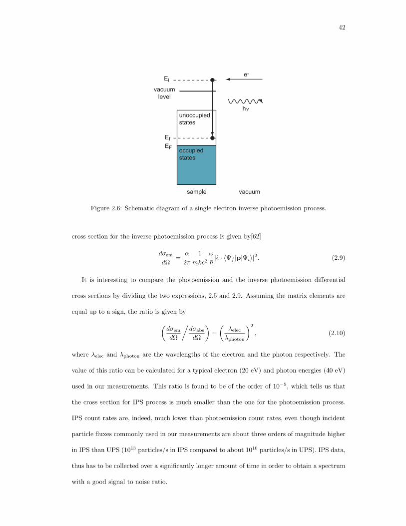
42
e-
hν
Ei
Ef
EFoccupied
states
unoccupied
states
sample vacuum
vacuum
level
Figure 2.6: Schematic diagram of a single electron inverse photoemission process.
cross section for the inverse photoemission process is given by[62]
dσem
dΩ=
α
2π
1
mkc2ω
~|ϵ · ⟨Ψf |p|Ψi⟩|2. (2.9)
It is interesting to compare the photoemission and the inverse photoemission differential
cross sections by dividing the two expressions, 2.5 and 2.9. Assuming the matrix elements are
equal up to a sign, the ratio is given by(dσem
dΩ
/dσabs
dΩ
)=
(λelec
λphoton
)2
, (2.10)
where λelec and λphoton are the wavelengths of the electron and the photon respectively. The
value of this ratio can be calculated for a typical electron (20 eV) and photon energies (40 eV)
used in our measurements. This ratio is found to be of the order of 10−5, which tells us that
the cross section for IPS process is much smaller than the one for the photoemission process.
IPS count rates are, indeed, much lower than photoemission count rates, even though incident
particle fluxes commonly used in our measurements are about three orders of magnitude higher
in IPS than UPS (1013 particles/s in IPS compared to about 1010 particles/s in UPS). IPS data,
thus has to be collected over a significantly longer amount of time in order to obtain a spectrum
with a good signal to noise ratio.

43
2.4.2 Inverse photoemission spectroscopy instrumentation
Inverse photoemission spectroscopy measurements can be done in two ways that require two
different modes of the electron source operation as well as different photon detector designs.
In an isochromat IPS system, only photons of a specific energy are collected and the incident
electron beam energy is varied to probe the range of final states of the sample. In a grating spec-
trometer system, which was used in the measurements reported in this thesis, an electron beam
of a fixed energy is incident onto a sample and photons of many energies are collected at once.
The number of photons measured at each photon energy represents the inverse photoemission
spectrum. Since the initial electron energy is kept fixed, the number of photons collected at
a certain photon energy is directly proportional to the number of electrons that decayed to a
particular unoccupied final state. This is, in turn, proportional to the density of unoccupied
states of the sample. As with the photoemission spectrum, the density of the unoccupied states
in the inverse photoemission spectrum is convoluted with the IPS cross section for each state,
given by Eq. (2.9). So, in principle, if the experimental objective is to determine the density of
the unoccupied states, either relative or absolute IPS cross section needs to be known.
The electron beam source, also called the electron gun, that we used for our measurements,
is based on the design of Stoffel and Johnson[64]. In this type of an electron gun, a planar BaO
cathode is heated by a filament and used as an electron source. Due to the elevated temperature,
electrons in the cathode occupy the energy levels up to the vacuum level, as shown in the electron
population curve for the cathode in Fig. 2.7. Voltages in the gun extract, decelerate and focus
the electrons from the cathode to a spot size of about 1 mm2 on the sample. The energy of
the electron beam is given by the voltage applied to the cathode plus the work function of the
cathode (Φc = 2.3 eV). The gun can produce a monoenergetic and well collimated electron
beam in the energy range from 4 to 50 eV. The energy spread within the beam is limited by the
thermal spread of the electrons in the hot cathode at a temperature of Tc and it is on the order
of kBTc. For a typical cathode temperatures of Tc ∼2600 K the energy spread of the electrons
in the beam is ∆E ∼ 0.2 eV.

44
eφc
eVB
EF,gun
EF,sample
cathode
DOS
e-Ei
hνmax
electron gun
cathode sample
Ee
Figure 2.7: Schematic energy diagram of an electron gun and a sample in the inverse photoe-mission spectroscopy.
The spectrograph system consists of two main parts. The concave spherical mirror with the
parallel grooves, called the grating, is used to spatially disperse photons coming from the sample
with respect to their energies. Photons in each energy channel are detected and counted using
position sensitive photon detector based on the series of microchannel plates and a resistive
anode encoder. The spectrograph system design is based on the Rowland circle, which employs
the dispersing and focusing properties of the grating.
In Fig. 2.8 the basic properties of the grating element are shown. The grating shown in
these figures has a radius Rm and it is tangent to Rowland circle, which is in the x-y plane and
has radius Rc, where Rm = 2Rc. If there is a photon source at the point A on the Rowland
circle with the defined wavelength λ1, rays that emanate from it in the x-y plane are refocused
by the grating to the point B on the Rowland circle. If there is a photon source at point A of a
different wavelength λ2 > λ1, rays in x-y plane will be refocused to point C located at a larger
dispersing angle on the Rowland circle. In this way grating is used to disperse photons with
respect to their energies.
Due to astigmatism, however, rays of wavelength λ1 that emanate from the point A but
have a component in z direction will be focused to a point D instead of point B. Thus, due to
astigmatism, the focal point of the rays of the same wavelength that originate from the same
point, but travel to the grating in different planes, is different.
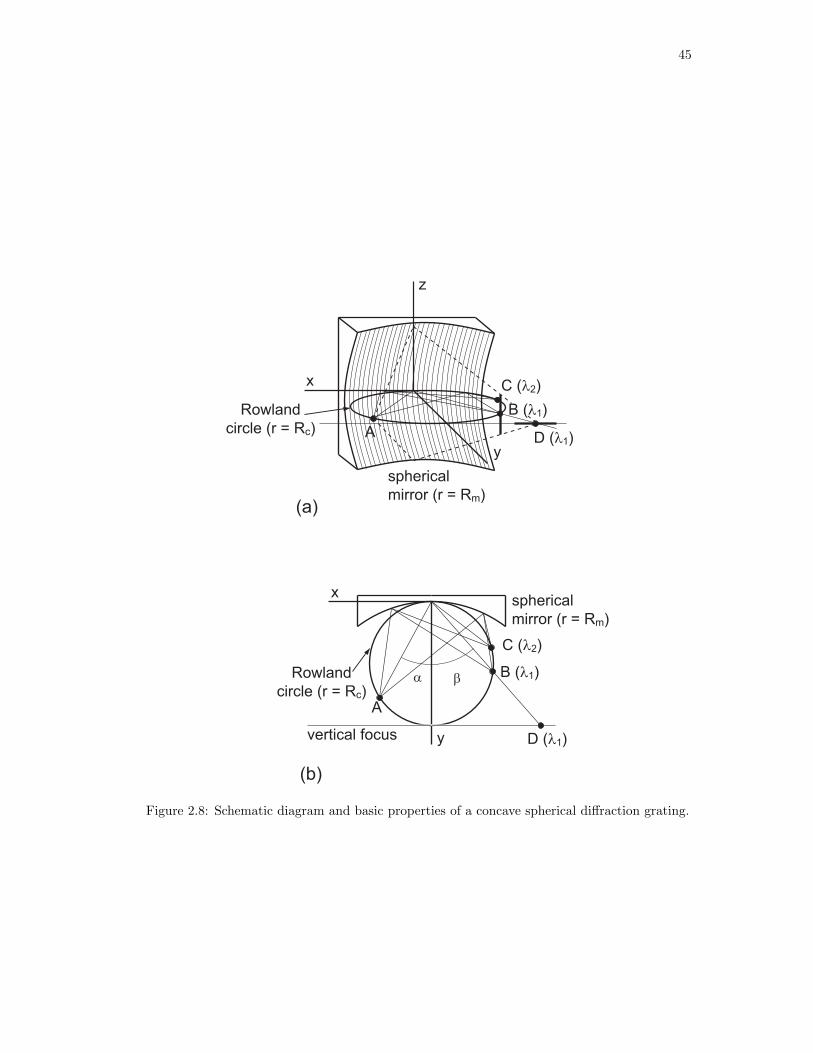
45
x
z
y
spherical
mirror (r = Rm)
Rowland
circle (r = Rc) A
B (λ1)
C (λ2)
D (λ1)
x
y
A
B (λ1)
C (λ2)
D (λ1)
α β
spherical
mirror (r = Rm)
Rowland
circle (r = Rc)
vertical focus
(a)
(b)
Figure 2.8: Schematic diagram and basic properties of a concave spherical diffraction grating.
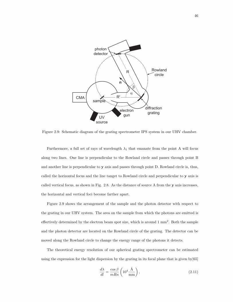
46
CMA
UV
source
electron
gun
diffraction
grating
Rowland
circle
photon
detector
sample
n
R
R'α
β
Figure 2.9: Schematic diagram of the grating spectrometer IPS system in our UHV chamber.
Furthermore, a full set of rays of wavelength λ1 that emanate from the point A will focus
along two lines. One line is perpendicular to the Rowland circle and passes through point B
and another line is perpendicular to y axis and passes through point D. Rowland circle is, thus,
called the horizontal focus and the line tanget to Rowland circle and perpendicular to y axis is
called vertical focus, as shown in Fig. 2.8. As the distance of source A from the y axis increases,
the horizontal and vertical foci become farther apart.
Figure 2.9 shows the arrangement of the sample and the photon detector with respect to
the grating in our UHV system. The area on the sample from which the photons are emitted is
effectively determined by the electron beam spot size, which is around 1 mm2. Both the sample
and the photon detector are located on the Rowland circle of the grating. The detector can be
moved along the Rowland circle to change the energy range of the photons it detects.
The theoretical energy resolution of our spherical grating spectrometer can be estimated
using the expression for the light dispersion by the grating in its focal plane that is given by[65]
dλ
dl=
cosβ
mRn
(104
A
mm
), (2.11)

47
where l is the distance measured along the detector in the dispersing direction, β is the angle of
the reflection of light with respect to the grating normal (Fig. 2.9), R is the distance between
the detector and the spherical grating in meters, m is the order of the interference and n is the
number of grooves per mm on the spherical grating. The dispersion of photons with respect to
their energies can be obtained from the above expression as
dE
dl=
hc
λ2
dλ
dl=
E2
hc
cosβ
mRn
(104
A
mm
). (2.12)
For our system, β = 25, m is 1, since we use the first order of the interference, R = 2Rc cosβ,
where Rc = 0.375 m is the radius of the Rowland circle and n=1200 lines/mm. As we can see,
the energy dispersion (Eq. (2.12)) depends on the photon energy E. In our IPS measurements,
for the incident electron beam energy Ep = 20.3 eV, we most often detect photons down to
about 14 eV. Energy dispersion for the 14 eV photons in our system is calculated to be 0.17
eV/mm, while for the 20 eV photons it is 0.36 eV/mm.
Our resolution is going to ultimately be limited by the electron beam spot size. It is,
therefore, useful to calculate a so-called spot-size limited resolution by taking dl in Eq. (2.12)
to be dl = Ms, where M is the magnification of the system and s is the electron beam spot
diameter on the sample. Magnification of the spherical grating is, further, given by
M =R cosα
R′ cosβ, (2.13)
where α is the angle of incidence of the light with respect to the grating normal and R′ is the
distance between the sample and the grating as shown in Fig. 2.9. For our system magnification
M is 1, and the electron spot diameter is abound 1 mm. Spot-size limited resolution for our
spectrometer system is then 0.17 eV and 0.36 eV for the 14 and the 20 eV photons, respectively.
Apart from the grating spectrometer, the spread of electrons originating from the electron
gun contributes to the total energy resolution of the inverse photoemission measurement. The
electron gun energy spread, caused by the thermal spread of electron energies emerging from a
hot cathode is estimated earlier in this chapter to be ∆E ∼ 0.2 eV. Since the two contributions
are added in quadrature to the total energy resolution, the latter can than be calculated to be

48
between 0.26 and 0.41 eV depending on the detected photon energy.
The photon detector consists of two microchannel plates, approximately 50 mm in diameter,
and the resistive anode encoder, as shown in Fig. 2.10. Microchannel plates are coated with
highly resistive glass material, and consists of regular array of tubes or slots, called microchan-
nels, leading from one to the other surface of the plate. The main purpose of the microchannel
plates is to convert an incoming photon signal to an electron signal and further amplify it via
secondary emission of electrons from the walls of the plate, in a very similar manner to the
channeltron in the CMA. The voltage difference at the opposite surfaces of the plates drives
emitted electrons through the channels from one surface to the other and causes the cascade
effect that multiplies the signal. The advantage of using microchannel plates is, however, the
spatial information of the signal provided by the existence of the densely distributed channels
on the surface of the plate.
microchannel
plates
resistive anode
encoder
preamps
electronics box(including analog to digital converter)
x (row)
y (column)
A
B C
D
3 MΩ
3 MΩ
3 MΩ
2 MΩ1 MΩ
10 MΩ
10 MΩ
10 MΩ
2 kV
0.005 µF
0.01 µF
Figure 2.10: Schematic diagram of a 2D position sensitive photon detector.
After the incoming photon signal is multiplied in this manner, a cloud of electrons that
emerged from the back surface of the second plate hits the anode. The anode is a sheet of
49
uniform resistance and current that passes through it is measured at each corner of the sheet,
labeled A, B, C and D in Fig. 2.10. The information about the photon position is obtained
from the current reading. The first coordinate is given by
X =IA + IB
IA + IB + IC + ID(2.14)
and the second coordinate by
Y =IB + IC
IA + IB + IC + ID. (2.15)
These two coordinates are expressed as two 8-bit digital numbers, so that each photon position
is expressed as the coordinates of one location on a 256 by 256 grid. The coordinates of each
photon are sent to the computer, which keeps a record of the number of photons that strike
detector at each location on the grid.
In the photon count array, the coordinate corresponding to the position along the Rowland
circle that is in the dispersion direction of the grating, is referred to as the horizontal channel
number. The other coordinate corresponds to the position normal to the plane of Rowland circle,
referred to as the vertical channel number. To obtain the IPS spectrum, for each horizontal
channel number photon counts in all the vertical channels are added since all of these photons
have the same energy. To be able to obtain the final IPS spectrum, however, this raw spectrum
needs to be modified in two ways. First, the horizontal channel numbers need to be calibrated
to the photon energy and the final state electron energy. Second, the so-called detector response
function needs to be divided from the raw spectrum. The detector response function includes
several contributions to the raw spectrum. One originates from the fact that the microchannel
plates are circular and intrinsically, there are more vertical channels for the horizontal channels
closer to the center of the plates than for the ones at the edges. Other contributions come
from the intrinsic inhomogeneities in the responses of the diffraction grating and the position
sensitive photon detector. IPS energy scale calibration procedure and the detector response
function measurement is described in detail in Appendix B.
50
2.5 Scanning Tunneling Microscopy
Scanning tunneling microscopy (STM), a technique developed in 1981 by Binnig and Rohrer[66],
is used to study the surface properties, in particular topography, of the conductive samples at the
atomic level. STM provides the information about the local properties of surfaces, in contrast
to many other surface sensitive techniques that measure surface properties averaged over a large
macroscopic area. In fact, out of all the experimental techniques we used in our study, STM is
the only surface sensitive technique that provided information about the local order of the dye
molecules adsorbed at metal and metal oxide surfaces.
The operating principle of the STM, a detailed description of which can be found elsewhere[67–
69], is based on the quantum mechanical tunneling of electrons across the potential barrier. In a
controlled manner, an atomically sharp metallic STM tip, usually made out of tungsten or Pt-Ir
alloy, is manipulated to approach the surface of the sample to the distance of less than 1 nm
with voltage applied between them. Under these conditions, the wave functions of the surface
and the tip atoms overlap and a tunneling current of electrons is established between them.
The tunneling current between the tip and sample can be measured and since its magnitude
exponentially depends[69] on the distance between the tip and the sample, STM can be used
for real space imaging of surfaces of the conductive samples at the atomic scale resolution. The
STM tip is, thus, extremely sensitive to the movements in the vertical direction. The lateral res-
olution of the STM, however, crucially depends on the sharpness of the STM tip. Furthermore,
to achieve good STM resolution, measured tunneling current between the tip and the sample
is used in a feedback loop to control the tip-sample distance while the tip scans the surface of
the sample. A good STM resolution is considered to be 0.1 nm in the lateral direction and 0.01
nm in the direction perpendicular to the surface of the sample. The tunneling conditions have
previously Fbeen achieved in air, liquid or vacuum environments, as well as at temperatures
down to 200 mK.
The position of the STM tip in all three directions is finely controlled by the piezoelectric
drive. Piezoelectric drive consist of mutually perpendicular piezoelectric transducers called x,
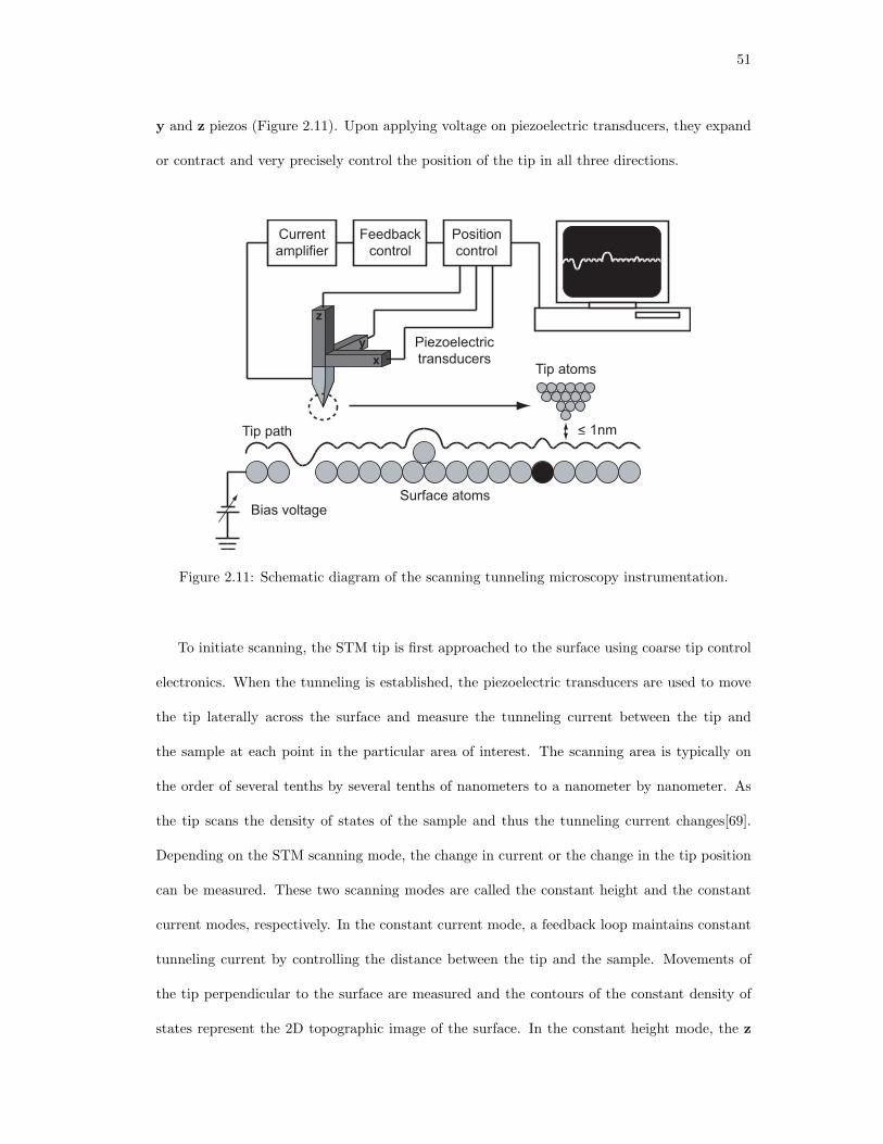
51
y and z piezos (Figure 2.11). Upon applying voltage on piezoelectric transducers, they expand
or contract and very precisely control the position of the tip in all three directions.
Current
amplifier
Feedback
control
Position
control
Piezoelectric
transducers
< 1nm
Surface atoms
Tip atoms
Bias voltage
y
z
Tip path
x
Figure 2.11: Schematic diagram of the scanning tunneling microscopy instrumentation.
To initiate scanning, the STM tip is first approached to the surface using coarse tip control
electronics. When the tunneling is established, the piezoelectric transducers are used to move
the tip laterally across the surface and measure the tunneling current between the tip and
the sample at each point in the particular area of interest. The scanning area is typically on
the order of several tenths by several tenths of nanometers to a nanometer by nanometer. As
the tip scans the density of states of the sample and thus the tunneling current changes[69].
Depending on the STM scanning mode, the change in current or the change in the tip position
can be measured. These two scanning modes are called the constant height and the constant
current modes, respectively. In the constant current mode, a feedback loop maintains constant
tunneling current by controlling the distance between the tip and the sample. Movements of
the tip perpendicular to the surface are measured and the contours of the constant density of
states represent the 2D topographic image of the surface. In the constant height mode, the z
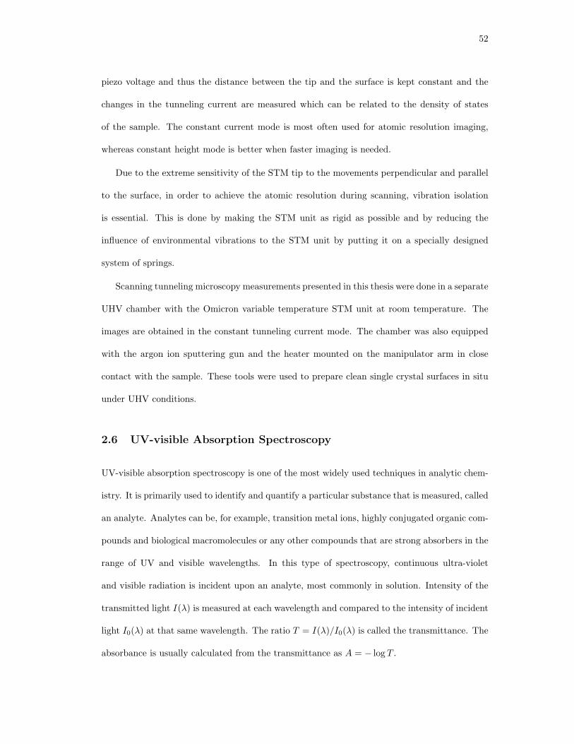
52
piezo voltage and thus the distance between the tip and the surface is kept constant and the
changes in the tunneling current are measured which can be related to the density of states
of the sample. The constant current mode is most often used for atomic resolution imaging,
whereas constant height mode is better when faster imaging is needed.
Due to the extreme sensitivity of the STM tip to the movements perpendicular and parallel
to the surface, in order to achieve the atomic resolution during scanning, vibration isolation
is essential. This is done by making the STM unit as rigid as possible and by reducing the
influence of environmental vibrations to the STM unit by putting it on a specially designed
system of springs.
Scanning tunneling microscopy measurements presented in this thesis were done in a separate
UHV chamber with the Omicron variable temperature STM unit at room temperature. The
images are obtained in the constant tunneling current mode. The chamber was also equipped
with the argon ion sputtering gun and the heater mounted on the manipulator arm in close
contact with the sample. These tools were used to prepare clean single crystal surfaces in situ
under UHV conditions.
2.6 UV-visible Absorption Spectroscopy
UV-visible absorption spectroscopy is one of the most widely used techniques in analytic chem-
istry. It is primarily used to identify and quantify a particular substance that is measured, called
an analyte. Analytes can be, for example, transition metal ions, highly conjugated organic com-
pounds and biological macromolecules or any other compounds that are strong absorbers in the
range of UV and visible wavelengths. In this type of spectroscopy, continuous ultra-violet
and visible radiation is incident upon an analyte, most commonly in solution. Intensity of the
transmitted light I(λ) is measured at each wavelength and compared to the intensity of incident
light I0(λ) at that same wavelength. The ratio T = I(λ)/I0(λ) is called the transmittance. The
absorbance is usually calculated from the transmittance as A = − log T .

53
Since an analyte will absorb photons of specific wavelengths from the incoming light, depend-
ing on its electronic structure, transmittance at these particular wavelengths will be reduced
and absorbance increased. A plot of absorbance versus wavelength, called the absorption spec-
trum, will show a set of peaks at the wavelengths unique to each analyte. Using the UV-visible
absorption spectrum the analyte can be identified and its concentration in solution can be
quantified.
The quantity that characterizes how strongly the molecule absorbs a certain wavelength is
called the extinction coefficient. The absorbance and the height of peaks in the UV-visible
absorption spectrum are directly proportional to that quantity. The extinction coefficient is, in
turn, proportional to the area of the molecule and the probability that the photon of a certain
wavelength will be absorbed when it strikes the molecule, called the transition probability.
We’ve derived this probability before in Section 2.3, Eq. (2.4). The same matrix element, that
can be written as in Eq. (2.8) governs the transition. From this we see that the transition
probability essentially depends on the the symmetries of the initial and final molecular orbitals.
In other words, orbitals involved in the transition need to obey strict selection rules, known as
dipole selection rules, for the transition probability between them to be non-vanishing. These
selection rules has to be taken into account when analyzing the absorption spectrum. Moreover,
the value of the matrix element depends on the overlap of the initial and the final state. The
better the overlap the greater the transition probability and the extinction coefficient.
2.6.1 UV-visible absorption spectroscopy instrumentation
A basic experimental setup for the UV-visible absorption spectroscopy is schematically shown
in Fig. 2.12. The main parts of the setup are the radiation source, the holder for the sample,
the diffraction grating or the prism as a part of the monochromator and the photon detector.
As the radiation source the tungsten filament and Xenon arc lamp are most often used.
They radiate with a constant intensity across a large range of wavelengths (200 - 2000 nm).
Other sources include the deuterium lamps that have constant spectrum in UV region and more

54
UV-visible
light sourceSlit 1
Diffraction
grating
Slit 2
Filter
Mirror 1
Mirror 2
Mirror 3
Half
mirror
Sample
beam
Reference
beam
Reference
cuvette
Sample
cuvette
Detector 2
Detector 1
I0
I
Lens 2
Lens 1
Figure 2.12: Schematic diagram of the UV-visible absorption spectroscopy instrumentation.
recently light emitting diodes with a constant spectrum in the visible region. The detectors are
most often a photomultiplier tube, a photodiode, a photodiode array or a charge-coupled device
(CCD). In the case where a photomultiplier tube or a photodiode is used, the diffraction grating
can rotate to select a particular wavelength at which the intensity will be measured by a detector.
For photodiode array and CCD the detection of all the wavelengths in the spectral range of the
spectrometer can be done simultaneously, so the diffraction grating can be fixed.
Most of the UV-visible spectrometers are so-called double-beam spectrometers where the
incident light is split into two beams before it reaches the sample. One beam is passed through
the sample and another one, called the reference beam, is usually passed through the solvent
used for the analyte solution. The intensities of two beams (I and I0) are measured and their
ratio is taken. Some double beam instruments have two detectors, so they can measure I and
I0 at the same time. In others a beam chopper is used which blocks one beam at the time.
The detector alternates, then, between measuring the sample beam and the reference beam in
synchronism with the chopper.
UV-visible absorption measurements reported in this thesis were done on a commercially

55
available VARIAN Cary-500 Scan UV-Vis-NIR spectrometer, that uses moveable diffraction
grating to scan over the wavelength range and the beam chopper with the photodiode for the
light intensity measurement. The range of this spectrometer spans ultra-violet, visible and
near-infrared wavelengths. In particular, for the measurements of the absorption spectra in
transmission its spectral range is from 175 nm to 3300 nm while for the measurements in
reflection it is from 175 nm to 2500 nm. Depending on the width of the slits through which the
reference and the sample beams are passing, the spectral resolution of this spectrometer can
be changed from 0.1 nm to 5 nm in the UV-visible region and from 0.4 nm to 20 nm in the
near-infrared region. The absorption spectroscopy measurements presented in this thesis are
done by our collaborators at the Chemistry Department of Rutgers University, Newark.
2.6.2 UV-visible absorption spectrum of porphyrins and porphyrin
derivatives
A discussion about the terminology and the transitions in the UV-visible absorption spec-
troscopy of the organic molecules in general can be found in Appendix C. In this section we
will concentrate on the UV-visible absorption spectroscopy of porphyrins, a central class of the
organic molecules in this thesis.
A typical UV-visible absorption spectra of free-base tetraphenylporphyrin (H2TPP) and zinc
tetraphenylporphyrin (ZnTPP) in solution are shown in Fig. 2.13(a) and (b) respectively.
The spectra consist of two bands, a higher energy (shorter wavelength) intense B band, also
called Soret band, and lower energy (longer wavelength) weak Q band. Soret band can be up
to 100 times more intense than Q band. Since porphyrin molecules do not contain lone pairs
of electrons, both B and Q bands in the UV-visible spectrum are assigned to π → π∗ singlet
transitions as shown for ZnTPP and H2TPP in Fig. 2.14(a) and Fig. 2.14(b), respectively.
ZnTPP Q band consists of two peaks denoted as Q(0,1) and Q(0,0). The shorter wavelength
(higher energy) peak is assigned to the transition into the higher vibronic state of the molecule
(Fig. 2.14(a)), since for great majority of porphyrins, the energy separation of Q(0,0) and
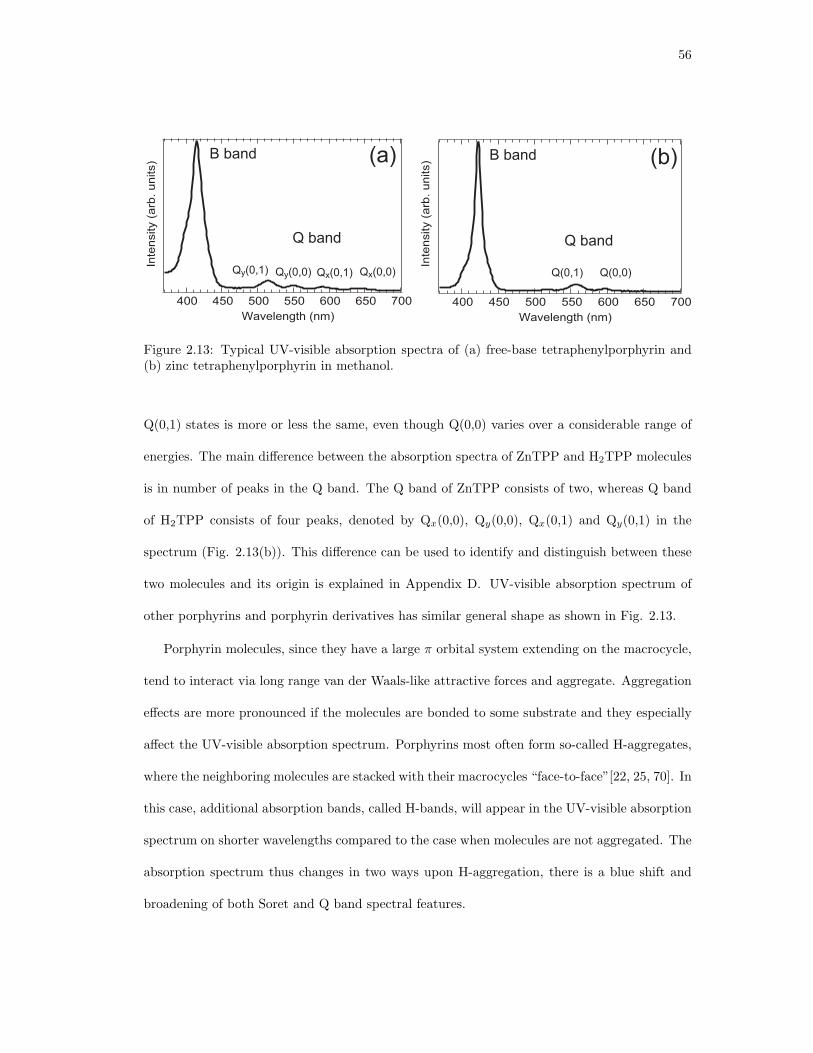
56
Inte
nsity (
arb
. units)
700650600550500450400
Wavelength (nm)
Inte
nsity (
arb
. u
nits)
700650600550500450400
Wavelength (nm)
(a) (b)B band B band
Q band Q band
Q(0,0)Q(0,1)Qy(0,0) Qx(0,0)Qx(0,1)Qy(0,1)
Figure 2.13: Typical UV-visible absorption spectra of (a) free-base tetraphenylporphyrin and(b) zinc tetraphenylporphyrin in methanol.
Q(0,1) states is more or less the same, even though Q(0,0) varies over a considerable range of
energies. The main difference between the absorption spectra of ZnTPP and H2TPP molecules
is in number of peaks in the Q band. The Q band of ZnTPP consists of two, whereas Q band
of H2TPP consists of four peaks, denoted by Qx(0,0), Qy(0,0), Qx(0,1) and Qy(0,1) in the
spectrum (Fig. 2.13(b)). This difference can be used to identify and distinguish between these
two molecules and its origin is explained in Appendix D. UV-visible absorption spectrum of
other porphyrins and porphyrin derivatives has similar general shape as shown in Fig. 2.13.
Porphyrin molecules, since they have a large π orbital system extending on the macrocycle,
tend to interact via long range van der Waals-like attractive forces and aggregate. Aggregation
effects are more pronounced if the molecules are bonded to some substrate and they especially
affect the UV-visible absorption spectrum. Porphyrins most often form so-called H-aggregates,
where the neighboring molecules are stacked with their macrocycles “face-to-face”[22, 25, 70]. In
this case, additional absorption bands, called H-bands, will appear in the UV-visible absorption
spectrum on shorter wavelengths compared to the case when molecules are not aggregated. The
absorption spectrum thus changes in two ways upon H-aggregation, there is a blue shift and
broadening of both Soret and Q band spectral features.

57
π
B
Q(0,1) Q(0,0)
π∗2
ground state
excite
d s
tate
s
ZnTPP molecule
π∗
π
BQy(0,1)
Qx(0,0)
1
π∗2
ground state
excite
d s
tate
s
H2TPP molecule
Qy(0,0)
Qx(0,1)
(a) (b)
π∗1
Figure 2.14: Schematic of the transitions for (a) zinc and (b) free-base tetraphenylporphyrinmolecules assigned to their UV-visible absorption spectra features.
These changes in the UV-visible absorption spectrum upon molecular aggregation are ex-
plained by a simple molecular exciton coupling model, the details of which can be found in
Appendix C. This model takes into account coupling of excitons, i.e. coupling of the transition
dipole moments on the neighboring molecules in the aggregate caused by van der Waals forces.
2.7 Reflection Electron Energy Loss Spectroscopy
Reflection electron energy loss spectroscopy (REELS) is used to study low energy excitation
processes in the sample. The measurement is performed by directing a monoenergetic beam of
electrons, with energies of few tenths to few thousands eV, onto a sample and recording the
energy spectrum of the electrons reflected after the interaction with the sample. Inelastic mean
free path (IMFP) of electrons and thus the interaction depth with the sample can be controlled
by changing the energy and the angle of the incoming electrons. In this way REELS can be
made extremely surface sensitive by using grazing incident angles and the electron energies
between 20-150 eV that fall in the universal curve minimum (Fig. 2.3). REELS can be, thus
used to study both surface and bulk excitations in the sample. Because of its surface sensitivity,

58
REELS is used mainly in UHV environments to prevent contamination of the surface during
the experiment.
In this thesis, surface sensitive REELS measurements were used to study the excitations
processes, specifically excitations of electrons across the band gap, in a monolayer or several
layers of porphyrin dye molecules adsorbed on single crystal metal and metal oxide surfaces.
2.7.1 Interpretation of REELS spectra and inelastic scattering cross
section
When electrons enter a solid, they interact with the constituent atoms through Coulomb inter-
action. As a result, some electrons are scattered, the direction of their momentum is changed
and in some cases they transfer energy to the the sample. A great majority of incoming fast
electrons will be elastically scattered from the atomic nuclei in the sample and deflected by a
large angle. Some fast electrons will transfer a small amount of their energy, on the order of a
fraction of an electronvolt, to the phonons in the sample. Since the energy loss in such events is
so small, these electrons can not be resolved from the elastically scattered electrons in REELS
and are thus called quasi-elastic. Finally, some incoming fast electrons will be inelastically
scattered from the atomic electrons. In such events an incoming fast electron transfers a part
or all of its energy to the atomic electron causing it to make a transition to a higher energy
state. Low energy electron transitions in a solid, called the outer-shell transitions, are the ones
studied in REELS. As shown in Fig. 2.15, some outer-shell inelastic processes in REELS can be
understood in terms of single electron excitations from the occupied states in the valence band
to the unoccupied states. This type of the transitions require energies on the order of 1 to 10
eV.
In an insulator or a semiconductor, a valence band electron can make an interband transition
across the energy gap. In the case of a metal, a conduction electron makes a transition to a
higher energy state, possibly in the same energy band (transition 1 in Fig. 2.15). Outer-
shell electrons can also be excited with sufficient energy to overcome the surface barrier and

59
K
L
EF
Evac
Light Auger
Outer-shell
excitations
De-excitations
1 2
Figure 2.15: Schematic diagram of a single electron excitation and de-excitation processes insolids.
escape the solid (transition 2 in Fig. 2.15). As opposed to single electron excitations, the
excitations of valence electrons can involve many electrons. This collective effect is known as
plasmon resonance and it’s usually depicted as an electron density oscillating with respect to
the stationary positive ion background in a solid. For majority of solids, plasmon excitation
energies lie in the range between 5 and 30 eV. Depending on the region of the sample where
plasmons are excited, they are either called bulk or surface plasmons, where surface plasmons
are restricted to a few surface layers of atoms. Since plasmons require electrons in the material
to freely move, these types of outer-shell excitations will be important for the materials where
electrons behave as free particles, like metals. In materials in which electrons are localized,
plasmon excitations are weak or nonexistent.
A general REELS spectrum will thus consists of two main regions, as shown in Fig. 2.16.
There is a primary or zero-loss peak that includes elastically or quasi-elastically scattered elec-
trons and the low energy loss region that includes the outer-shell excitations of valence electrons,
i.e. single electron and/or plasmon excitations. In the case of metals, the most prominent fea-
tures in the low energy loss region of REELS spectrum will come from the surface and bulk
60
Inte
nsity (
arb
. u
nits)
20151050
Energy loss (eV)
zero-loss
peak
outer-shell excitationsexcitations across
the band gap and/or
plasmons
Figure 2.16: A typical shape of REELS spectrum.
plasmon excitations. However, in case of the metal oxides and the organic dye molecules, most
prominent features are attributed to the excitations of electrons across the band gap or the
gap between the highest occupied molecular orbital (HOMO) and lowest unoccupied molecular
orbital (LUMO).
In REELS measurements electrons, emerging from the sample are collected in the reflection
geometry, i.e. the electron source and the detector are facing the same surface of the sample.
Since the excitations of valence and conduction electrons occur predominantly at small angles,
there has to be a large angle elastic event before or after the inelastic event that causes the
electron to be reflected back. This process is schematically illustrated in Fig. 2.17. An electron
with the momentum k0 and energy E0 enters the sample along the normal and either inelastically
scatters at the point O and then elastically scatters at P or it first elastically scatters at point
P’ and then inelastically at point O’.
According to Bethe theory[71], the differential cross section for inelastic scattering per unit
energy and per unit solid angle is written within the single-electron model and the first Born

61
P'P
O O'
e- e-
Figure 2.17: Schematic diagram of scattering processes in a solid during REELS measurements.
approximation as[71]
∂2σ
∂Ω∂E=
4
a20q4
∑Ψf
∣∣∣∣∣∣⟨Ψf
∣∣∣∣∣∣∑rj
exp(iq · rj)
∣∣∣∣∣∣Ψi
⟩∣∣∣∣∣∣2
δ(Ef − Ei −∆E), (2.16)
where a0 is Bohr radius, q is the change in the incident electron momentum, rj is the position
vector of the electron participating in transition and Ψi and Ψf are the initial and the final states
with energy Ei and Ef respectively. In the limit of small scattering angles and small energy
transfers (q · rj ≪ 1), the dipole approximation can be applied to the exponential function in
the matrix element in Eq. (2.16). Since the final and initial states are orthogonal to each other,
the first order matrix element will be proportional to
Mif ∝
∣∣∣∣∣∣⟨Ψf
∣∣∣∣∣∣∑rj
q · rj
∣∣∣∣∣∣Ψi
⟩∣∣∣∣∣∣2
(2.17)
Similar matrix elements were derived in previous sections for the photon-electron interaction
(Eqs. 2.5 and 2.7). From this we can conclude that the fast electron in REELS is behaving
somewhat similar to the photon in the absorption spectroscopies (Section 2.6). This correspon-
dence between REELS and UV-visible absorption spectra was observed experimentally for the
organic molecules as well[72]. One crucial difference is that electron can transfer any arbitrary
amount of energy, whereas photon can either give all or none of its energy to the electron in
the sample.
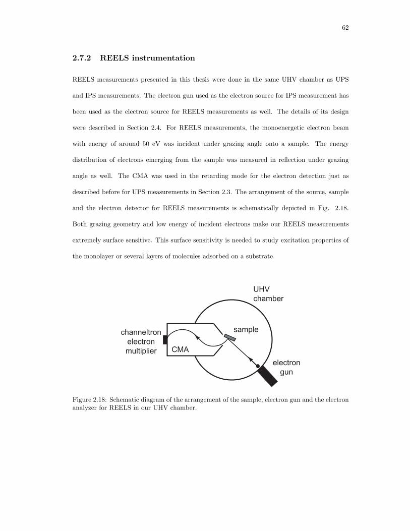
62
2.7.2 REELS instrumentation
REELS measurements presented in this thesis were done in the same UHV chamber as UPS
and IPS measurements. The electron gun used as the electron source for IPS measurement has
been used as the electron source for REELS measurements as well. The details of its design
were described in Section 2.4. For REELS measurements, the monoenergetic electron beam
with energy of around 50 eV was incident under grazing angle onto a sample. The energy
distribution of electrons emerging from the sample was measured in reflection under grazing
angle as well. The CMA was used in the retarding mode for the electron detection just as
described before for UPS measurements in Section 2.3. The arrangement of the source, sample
and the electron detector for REELS measurements is schematically depicted in Fig. 2.18.
Both grazing geometry and low energy of incident electrons make our REELS measurements
extremely surface sensitive. This surface sensitivity is needed to study excitation properties of
the monolayer or several layers of molecules adsorbed on a substrate.
CMA
electron
gun
samplechanneltron
electron
multiplier
UHV
chamber
Figure 2.18: Schematic diagram of the arrangement of the sample, electron gun and the electronanalyzer for REELS in our UHV chamber.
63
2.8 Near-Edge X-ray Absorption Fine Structure
Compared to other types of X-ray spectroscopies, near-edge X-ray absorption fine structure
(NEXAFS) is a relatively young technique. Its development crucially depended on the devel-
opment of the continuous, high intensity X-ray sources that are now available at synchrotrons.
NEXAFS probes the absorption of X-ray radiation by exciting the core electron to unoccupied
bound or continuum states. The particular X-ray photon energies at which the absorption is
suddenly increased are called the edges or ionization thresholds and they correspond to the
transition of electrons from the core levels to a set of the final states. For example, for the
transitions from the 1s level, the corresponding edge is called the K-edge. NEXAFS spectra
often exhibit strong and distinctive features in the energy region just below or up to 50 eV above
the ionization threshold. The shape and the energy position of these fine structure features are
extremely sensitive to the chemical environment. NEXAFS can, thus give us the information
about the composition and the bonding environment of each element in the sample. Further-
more, by using polarized synchrotron radiation, NEXAFS can also be used to determine the
orientation of molecules adsorbed at a surface. This was the primary reason why we performed
the NEXAFS measurements on the metal oxide samples sensitized with dye molecules that are
presented in this thesis.
2.8.1 NEXAFS measurement and interpretation of NEXAFS spectra
The origin of NEXAFS features is schematically shown in Fig. 2.19. The effective potential and
corresponding K-edge NEXAFS spectrum for a diatomic π-bonded molecule are shown. Around
the ionization threshold, resonant features are superimposed on a step-like shape. These features
correspond to the transitions of an electron from the initial occupied to the final unoccupied
molecular states where an incoming X-ray photon supplies the energy needed for the transi-
tion. For a neutral molecule, unoccupied π∗ and σ∗ orbitals are most often found above the
vacuum level. However, after excitation of a core electron, a core hole is present on a molecule,
making the molecule positively charged, which influences the energy of the unoccupied orbitals.
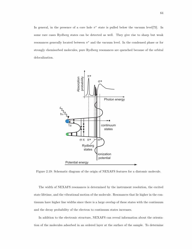
64
In general, in the presence of a core hole π∗ state is pulled below the vacuum level[73]. In
some rare cases Rydberg states can be detected as well. They give rise to sharp but weak
resonances generally located between π∗ and the vacuum level. In the condensed phase or for
strongly chemisorbed molecules, pure Rydberg resonances are quenched because of the orbital
delocalization.
1s
σ σ∗π π∗
σ∗
π∗
hν
Rydberg
states
continuum
states
ionization
potential
Ab
so
rptio
n
pro
ba
bili
ty
Photon energy
Potential energy
Figure 2.19: Schematic diagram of the origin of NEXAFS features for a diatomic molecule.
The width of NEXAFS resonances is determined by the instrument resolution, the excited
state lifetime, and the vibrational motion of the molecule. Resonances that lie higher in the con-
tinuum have higher line widths since there is a large overlap of these states with the continuum
and the decay probability of the electron to continuum states increases.
In addition to the electronic structure, NEXAFS can reveal information about the orienta-
tion of the molecules adsorbed in an ordered layer at the surface of the sample. To determine

65
molecular orientation using NEXAFS, linearly polarized monochromated X-ray radiation, avail-
able at synchrotrons, is directed onto a sample and the absorption for different X-ray energies
around a particular ionization edge is measured. The absorption and the intensity of the NEX-
AFS features will change depending on the incident angle of linearly polarized radiation with
respect to the surface of the sample. For the organic molecules, angular dependance of the
K-edge resonances, in particular sharp π resonances, of carbon and/or nitrogen is most often
used. A detailed discussion about the determination of the orientation of the organic molecules
adsorbed at the surface using NEXAFS can be found in Appendix E. Briefly, for a particular
transition, angular dependance of NEXAFS cross section (Eq. (2.5)) is given by the scalar prod-
uct between the polarization vector of the incoming electric field and the matrix element called
the transition dipole moment vector M (Eq. (2.7)). If the electric field vector is thus parallel
to the transition dipole moment vector the NEXAFS cross section will be maximal, while if the
electric field vector is perpendicular to the transition dipole moment vector, the cross section
will be zero. In between these two extremal angles, the intensity varies as cos2 δ, where δ is
the angle between the electric field and the transition dipole moment vector. For the K-edge
of carbon, it turns out, as shown in Appendix E, that the transition dipole moment vector M
points along the lobes of the final state π∗ or σ∗ molecular orbitals. When the incident electric
field is thus parallel to either π∗ or σ∗ orbitals of the molecule, intensity of a corresponding
resonance in the NEXAFS spectrum of carbon K-edge will be maximal. In contrast, when the
incident electric field is perpendicular to either π∗ or σ∗ orbitals of the molecule, intensity of a
corresponding resonance in the NEXAFS spectrum of carbon K-edge will vanish. This makes
the basis for the determination of the orientation of the organic molecules adsorbed at the
surface of the sample.
2.8.2 NEXAFS measurements and instrumentation
During a NEXAFS measurement, the sample is irradiated with monochromatic X-rays. The
energy of X-rays is varied around a particular ionization edge using a monochromator. As

66
an X-ray photon enters the sample, it is absorbed by a core electron, as shown in Fig. 2.20.
Core electron is promoted to an unoccupied bound states or it is emitted from the sample as a
photoelectron. The core hole that is left behind is filled with an electron from a higher occupied
state. The electron can either emit a photon, in the process called fluorescence, or transfer
its energy to another electron in an atom, in a process called the Auger process. The Auger
electron is, just as a fluorescent photon, emitted from the sample.
Both fluorescence and the Auger process are direct measure of the existence of a core hole
created in X-ray absorption and therefore a measure of the absorption cross section. However,
in general, the probability for an Auger decay increases as the energy difference between the
states that are involved in the process decreases. Lighter elements will thus have much higher
probability of relaxing via Auger than via fluorescence process. The detection of Auger electrons
for the organic molecules, that contain lighter elements, is thus preferred over the detection of
fluorescent photons. Another advantage of the Auger electron detection in NEXAFS compared
to fluorescence photon detection is that the electrons have much shorter IMFP compared to
photons and thus Auger electron detection provides greater surface sensitivity.
Evac
CB
VB
Promoting a core level
electron to unoccupied states
De-excitaion processes
Flourescence Auger process
CB
VB
CB
VB
Evac Evac
Figure 2.20: Schematic diagram of electron excitation and de-excitation processes in NEXAFS.
67
Electrons coming from the sample in a NEXAFS process can be detected in three ways. One
way is to measure the number of Auger electrons emerging from the sample using the electron
analyzer, like cylindrical mirror analyzer (CMA), described in Section 2.3. Since the energy of
Auger electrons is independent of the photon energy, the CMA can be set to a particular Auger
peak energy and simply count the number of electrons as the energy of incident photons is
swept. Changes in the detected number of electrons, or intensity of the Auger peak, are directly
proportional to the NEXAFS absorption cross section. This mode of detection is called Auger
electron yield (AEY).
Apart from the primary Auger electrons emerging from the sample, there are also Auger
electrons that are inelastically scattered on the way out of the sample and thus have lower
kinetic energies. Since the energy of the Auger electrons is independent of the photon energy,
the distribution of the inelastically scattered Auger electrons will follow the changes of in the
intensity of the primary Auger peak. This is utilized in partial electron yield (PEY) detection
where all electrons with the kinetic energy above some threshold energy are detected. The
threshold energy can be suitably chosen to avoid the detection of primary photoelectrons. In
the analyzer, the filtering of electrons according to their energy is done by simply applying
retardation voltage before the electron detector.
Finally, all electrons coming from the sample, including primary and secondary photoelec-
trons and primary and secondary Auger electrons can be detected. This mode of detection is
called total electron yield (TEY). Both PEY and TEY modes of detection are simpler since they
don’t require an electron energy analyzer. However, when high surface sensitivity is needed,
AEY is a preferred method of detection since IMFP for Auger electrons in NEXAFS process
(with energies of several hundreds eV) is 1 nm or less. For our NEXAFS measurements PEY
detection was used. The PEY detector is schematically shown in Fig. 2.21. It consists of two
metallic grids, insulated from each other and two channelplates for electron multiplication, that
work in a similar way as a channeltron in CMA. The first grid is typically grounded and the
second grid is at the retardation voltage that sets the energy cutoff for the electrons that are

68
ceramic
housing
collector
(V6)
ceramic
spacer
ring
contact
(V5)
2nd channel
plate
ring
contact
(V4)
1st channel
plate
ring
contact
(V3)
ceramic
spacer
2nd metal
grid
(V2)
ceramic
spacer
1st metal
grid
(V1)
ceramic
spacer
compression
spring
coverplate
Figure 2.21: Schematic diagram of a partial electron yield detector.
filtered from the spectrum.
2.9 Computational methods
As a part of this thesis, we performed ab-initio quantum chemistry calculations to better un-
derstand the electronic structure and the energy level alignment at the interfaces between
tetraphenylporphyrin dye molecules and the metal or metal oxide substrates. In particular,
these calculations were done to identify the features of the adsorbed molecules measured in UV
and inverse photoemission spectroscopy (UPS and IPS) and to assign these features to a specific
bound molecular orbital or a set of orbitals.
Ab-initio quantum chemistry calculations were done for the isolated molecules in the frame-
work of density function theory (DFT) using a semi-empirical Becke, three parameter, Lee-
Yang-Parr (B3LYP) exchange-correlation functional to describe the electron-electron interac-
tion. Several different split-valence localized basis sets were used in the calculation. The basic
ideas of DFT and a particular expression for B3LYP functional, as well as the details about the
basis sets used in the calculations can be found in Appendix F.
69
We used General Atomic and Molecular Electronic Structure System (GAMESS) software
package[74] that is freely available online2 to run our DFT calculations. This software package
has been designed specifically for ab-initio molecular quantum chemistry calculations and has
capabilities of computing a variety of molecular properties. In particular, we were interested in
calculating the equilibrium geometry, electronic states, and associated molecular orbitals of the
isolated, i.e. not bonded to the surface tetraphenylporphyrin derivative dye molecules.
Molecular states that were obtained as a result of the calculations in GAMESS were given as
the set of discrete molecular levels. To ease the comparison of the theoretical and experimental
UPS and IPS spectra, the theoretical spectra were modified in three ways. First, experimental
broadening in UPS and IPS spectra was “simulated” by broadening each discrete molecular state
in the theoretical spectra by a Gaussian function. Full width at half maximum (FWHM) of the
Gaussian function was chosen depending on the width of the states in UPS and IPS spectra.
Furthermore, all Gaussian functions centered at the calculated molecular state energies were
summed up to obtain calculated molecular DOS. Second, having in mind that DFT calculations
tend to underestimate energy band gaps so-called scissor operation has been used to rigidly
shift the empty states with respect to the filled states in the calculated DOS and increase the
calculated band gap by a certain value. This value was chosen so that most experimental and
theoretical features coincide well after the band gap increase. Third, calculated DOS was rigidly
shifted so that the zero of energy coincides with the Fermi energy obtained from the experiment.
There is, however, one crucial difference between the theoretical and experimental spectra
that needs to be taken into account when comparing the two. Contrary to the measured UPS
and IPS spectra, cross section effects are not included in the calculated density of states (DOS)
of the isolated molecules. Generally, relative intensities of peaks in the UPS spectra will thus
differ from the relative intensities of peaks in the calculated DOS.
2http://www.msg.ameslab.gov/gamess/

70
Chapter 3
Electronic structure, energy alignment and molecular
packing of zinc(II)tetraphenylporphyrin derivatives
adsorbed on TiO2(110) and ZnO(1120) surfaces
3.1 Introduction
The charge transport through the dye-sensitized solar cell (DSSC) and consequently the pho-
tocurrent generation strongly depends on the interaction between the cell components and the
kinetics of the electronic processes in the cell. Since the electron-hole pair created by the light
absorption is localized on the molecule and separated at the molcule/dye interface, the charge
injection and charge recombination processes will crucially depend on the nature of the inter-
face between the dye molecule and the oxide substrate. In particular, the molecular adsorption
geometry at the oxide surface, the molecule-molecule interaction and energy alignment of the
molecular levels with respect to the substrate band structure all need to be considered to fully
understand the charge transfer mechanisms in these cells.
In recent years metalloporphyrins, especially zinc(II)tetraphenylporphyrin (ZnTPP) detiva-
tives, have been recognized as attractive candidates for the dye sensitizers in DSSCs. [9, 12, 23]
The light absorption in porphyrins can be thought of, in the simplest approximation, as the
transition of an electrons from the degenerate or nearly degenerate HOMOs to the LUMOs of
the molecule. To form a tetraphenylporphyrin molecule, four phenyl rings are attached to the
main porphyrin ring. However, due to steric interaction between the hydrogens on the phenyl
and hydrogens on the porphyrin rings, the two rings are oriented nearly perpendicular to one
another[21, 75]. This geometric restraint causes the π systems on the two rings of the molecule
71
to be almost completely electronically decoupled. The light absorption properties of the TPP
molecules can be thus very well approximated by those of the porphyrins[10]. Moreover, owing
to this weak coupling, adding functional groups to the phenyl rings of a TPP molecule is not
expected to have a significant impact on its optical absorption properties. TPP derivatives, thus
present an interesting case where, through a judicious choice of phenyl functional groups, the
molecular adsorption geometry on a surface and molecule-molecule interaction, can be modified
without altering its optical absorption properties. These properties of TPP have been exploited
by Galoppini and coworkers in a series of studies investigating the optical absorption of ZnTPP
derivatives attached to the surfaces of several wide-band gap semiconductor oxides[22, 25, 76].
In their work, the phenyl rings of a series of ZnTPP molecules were functionalized either to
change the bonding geometry to the surface or to modify the molecule-molecule steric inter-
actions. As expected from the above considerations, the experimentally observed absorption
properties of these ZnTPP derivatives in solution were found to be similar to those of ZnP.
However, when adsorbed onto ZnO, TiO2 or ZrO2 surfaces, strong perturbations of the optical
absorption spectra were observed for the class of molecules that allow face-to-face stacking of
the porphyrin macro-cycles[22, 25].
In the study presented in this chapter, we have chosen four ZnTPP derivatives, schematically
shown in Fig. 3.1, for which the particular functionalization of the phenyl rings with the
carboxylic acid (COOH) anchoring groups is expected to lead to different adsorption geometries
when the molecules are bound to the surface of an oxide. In particular, the molecule ZnTPP-Ipa
molecule of Fig. 3.1 possesses two COOH anchoring groups on one phenyl ring, and thus can
only bind to the surface through one phenyl ring. As a consequence, ZnTPP-Ipa is expected to
adsorb nearly upright, with a large angle between the plane of the porphyrin ring and the plane
of the substrate surface[9, 22]. A similar adsorption geometry is expected for the ZnTMP-Ipa
molecule of Fig. 3.1 as it also possesses the same functionalization as the ZnTPP-Ipa. However,
the other three phenyl groups in the molecule are functionalized by methyl (CH3) groups which
are expected to act as spacers between the molecules thus preventing dye aggregation at high
72
coverage[22]. The third and the fourth molecule, p-ZnTCPP and m-ZnTCPP, have all four
phenyl rings functionalized with one COOH anchoring group, however, in a different positions
on the phenyl rings. The COOH anchoring groups are located in the para position in the p-
ZnTCPP molecules, while in the m-ZnTCPP molecule they are located in the meta position on
the phenyl rings. This is expected to change the binding geometry from the upright, for thep-
ZnTCPP molecule, to the flat with respect the surface, for the m-ZnTCPP[22, 25, 77]. Since
the p- and the m-ZnTCPP molecules are expected to have similar electronic structures, but are
expected to display drastically different adsorption geometries owing they were chosen for the
molecular geometry study in NEXAFS. All four types of molecules have been synthesized by our
collaborators at Elena Galoppini’s group from Chemistry Department at Rutgers University,
Newark.
The adsorption geometry and the electronic structure of the molecule/substrate interface are
directly probed and compared to UV-visible absorption properties and resulting electron trans-
fer efficiency. The occupied and unoccupied electronic structure (particularly the HOMOs and
LUMOs energy alignment with respect to the substrate band edges) of four ZnTPP-derivatives
on the single crystal TiO2(110) and ZnO(1120) surfaces has been studied using a combination
of X-ray and UV photoemission spectroscopies (XPS and UPS) and inverse photoemission spec-
troscopy (IPS) in a single ultra-high vacuum (UHV) chamber. The full energy diagram of the
molecule-surface interface has been extracted from the experimental electronic structure with
the aid of density functional theory (DFT) calculations. In addition, the adsorption geometries
of two representative molecules (p- and m-ZnTCPP) have been explored using near edge X-ray
absorption spectroscopy (NEXAFS), and supplemented with scanning tunneling microscopy
(STM) as a local probe on the TiO2(110) surface. Our results illustrate the need for a compre-
hensive approach towards the characterization of these complicated molecule/oxide interfaces,
and show that the presence of optical absorption features associated with the formation of the
aggregates on the surface are directly correlated with molecules binding in an upright geometry,
enabling molecule-molecule dipolar interaction.
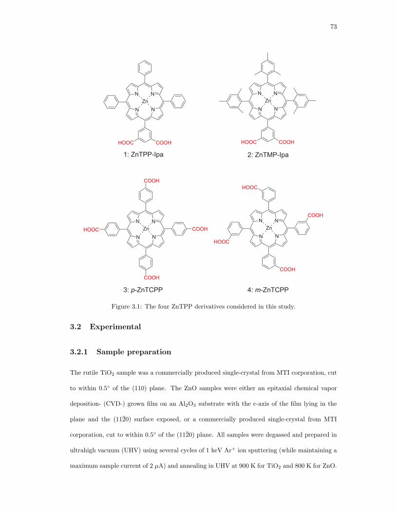
73
N
N N
N
Zn
N
N N
N
Zn
N
N N
N
Zn
N
N N
N
Zn
HOOC COOH HOOC COOH
COOH
COOH
COOH
HOOC
COOH
COOH
HOOC
HOOC
1: ZnTPP-Ipa 2: ZnTMP-Ipa
3: p-ZnTCPP 4: m-ZnTCPP
Figure 3.1: The four ZnTPP derivatives considered in this study.
3.2 Experimental
3.2.1 Sample preparation
The rutile TiO2 sample was a commercially produced single-crystal from MTI corporation, cut
to within 0.5 of the (110) plane. The ZnO samples were either an epitaxial chemical vapor
deposition- (CVD-) grown film on an Al2O3 substrate with the c-axis of the film lying in the
plane and the (1120) surface exposed, or a commercially produced single-crystal from MTI
corporation, cut to within 0.5 of the (1120) plane. All samples were degassed and prepared in
ultrahigh vacuum (UHV) using several cycles of 1 keV Ar+ ion sputtering (while maintaining a
maximum sample current of 2 µA) and annealing in UHV at 900 K for TiO2 and 800 K for ZnO.

74
The cleanliness of the surfaces was checked using XPS, and the surface termination was assessed
by low energy electron diffraction. Following an ex-situ 20 minutes sensitization in a solution of
dye in anhydrous ethanol, and rinsing with anhydrous ethanol to prevent dye accumulation, the
sample was reintroduced into the UHV analysis chamber. Synthesis of all ZnTPP derivatives
studied here was performed by our collaborators from Elena Galoppini’s group at the Chemistry
Department, Rutgers University at Newark. The details about the synthesis procedure can be
found elsewhere[22, 25, 77].
3.2.2 Spectroscopic methods
Ultraviolet, X-ray and inverse photoemission spectroscopy measurements were performed in
a single UHV experimental system. More details about the spectroscopic measurements and
instrumentation can be found in Sections 2.3 and 2.4. The overall instrumental energy resolution
for the UPS and IPS is estimated to be better than 0.3 eV and 0.6 eV, respectively.
Angle-dependent NEXAFS experiments, the details of which can be found in Section 2.8,
were performed at the U7A beamline of the National Synchrotron Light Source in UHV. The
absorption spectra were recorded in the partial yield mode at the N 1s and C 1s edges. The
incident radiation is characterized by a linear polarization in the order of 80 % and by an energy
resolution better than 0.2 eV.
3.2.3 Scanning probe microscopy
The scanning tunneling microscopy (STM) measurements were performed in a separate UHV
chamber using an Omicron variable temperature STM (VT-STM) and an Omicron low temper-
ature STM (LT-STM) at either 300 K or 90 K. Explanation of the STM measurement procedure
and the STM instrumentation can be found in Section 2.5. Due to the solution-sensitization
approach used in this study, the pristine oxides surfaces have to be removed from the UHV
chamber to be sensitized. This step complicates the STM measurements, as unwanted adsor-
bates can profoundly alter imaging. To address this issue, we have dosed the TiO2(110) surface

75
with pivalic acid vapors in the UHV chamber after preparing an atomically flat and well-ordered
surface. This step forms a well-ordered pivalate layer that acts as a robust passivation layer, pro-
tecting the surface from the atmospheric contaminations, while allowing COOH functionalized
dyes to replace the pivalate layer in a solution of dye[78, 79]. We have adopted this approach
with both the m-ZnTCPP and p-ZnTCPP dyes in order to study the adsorbate geometry at
low molecular coverage and thus identify individual adsorbed species.
3.2.4 Computational
Electronic structure calculations, the details of which can be found in Section 2.9, were per-
formed using GAMESS(US)[74] software package on the molecules in gas phase, i.e. not bonded
to the surface. Geometries in local minima on the potential energy surface were calculated with
a 6-31G* basis set[80]. The density of states (DOS) was produced by performing a sum of the
individual electronic states convoluted with a 1.2 eV full width at half maximum Gaussian func-
tion. This particular Gaussian width was chosen because it best “simulated” the experimental
broadening of the electronic states which made the comparison with the experimental UPS and
IPS spectra easier.
3.3 Results and discussion
3.3.1 Energy level alignment
Ab-initio electronic structure
Calculations of the molecular geometry for the four dyes were carried out in a fixed symmetry
(C2v for ZnTPP-Ipa, Cs for ZnTMP-Ipa and C4v for p-ZnTCPP and m-ZnTCPP). Within the
basis set and functional employed here, optimized geometries obtained are in a good agreement
with previous work on similar molecules[21, 81, 82]. In all cases, the phenyl groups are found
perpendicular to the main ZnP ring, consistent with a weak electronic coupling between the
inner ZnP portion of the molecule and the outer phenyls. Owing to this weak coupling, it is
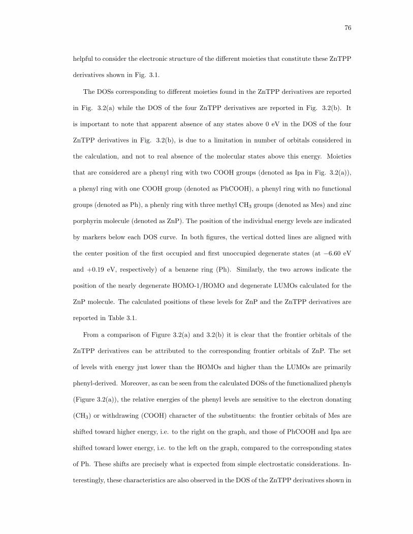
76
helpful to consider the electronic structure of the different moieties that constitute these ZnTPP
derivatives shown in Fig. 3.1.
The DOSs corresponding to different moieties found in the ZnTPP derivatives are reported
in Fig. 3.2(a) while the DOS of the four ZnTPP derivatives are reported in Fig. 3.2(b). It
is important to note that apparent absence of any states above 0 eV in the DOS of the four
ZnTPP derivatives in Fig. 3.2(b), is due to a limitation in number of orbitals considered in
the calculation, and not to real absence of the molecular states above this energy. Moieties
that are considered are a phenyl ring with two COOH groups (denoted as Ipa in Fig. 3.2(a)),
a phenyl ring with one COOH group (denoted as PhCOOH), a phenyl ring with no functional
groups (denoted as Ph), a phenly ring with three methyl CH3 groups (denoted as Mes) and zinc
porphyrin molecule (denoted as ZnP). The position of the individual energy levels are indicated
by markers below each DOS curve. In both figures, the vertical dotted lines are aligned with
the center position of the first occupied and first unoccupied degenerate states (at −6.60 eV
and +0.19 eV, respectively) of a benzene ring (Ph). Similarly, the two arrows indicate the
position of the nearly degenerate HOMO-1/HOMO and degenerate LUMOs calculated for the
ZnP molecule. The calculated positions of these levels for ZnP and the ZnTPP derivatives are
reported in Table 3.1.
From a comparison of Figure 3.2(a) and 3.2(b) it is clear that the frontier orbitals of the
ZnTPP derivatives can be attributed to the corresponding frontier orbitals of ZnP. The set
of levels with energy just lower than the HOMOs and higher than the LUMOs are primarily
phenyl-derived. Moreover, as can be seen from the calculated DOSs of the functionalized phenyls
(Figure 3.2(a)), the relative energies of the phenyl levels are sensitive to the electron donating
(CH3) or withdrawing (COOH) character of the substituents: the frontier orbitals of Mes are
shifted toward higher energy, i.e. to the right on the graph, and those of PhCOOH and Ipa are
shifted toward lower energy, i.e. to the left on the graph, compared to the corresponding states
of Ph. These shifts are precisely what is expected from simple electrostatic considerations. In-
terestingly, these characteristics are also observed in the DOS of the ZnTPP derivatives shown in
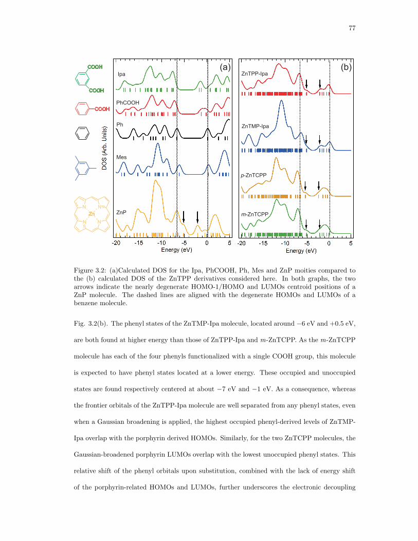
77
COOHCOOH
COOHCOOH
COOH
N
N N
N
Zn
ZnTPP-IpaIpa
PhCOOH
Ph
ZnP
Mes
ZnTMP-Ipa
p-ZnTCPP
m-ZnTCPP
(a) (b)
Figure 3.2: (a)Calculated DOS for the Ipa, PhCOOH, Ph, Mes and ZnP moities compared tothe (b) calculated DOS of the ZnTPP derivatives considered here. In both graphs, the twoarrows indicate the nearly degenerate HOMO-1/HOMO and LUMOs centroid positions of aZnP molecule. The dashed lines are aligned with the degenerate HOMOs and LUMOs of abenzene molecule.
Fig. 3.2(b). The phenyl states of the ZnTMP-Ipa molecule, located around −6 eV and +0.5 eV,
are both found at higher energy than those of ZnTPP-Ipa and m-ZnTCPP. As the m-ZnTCPP
molecule has each of the four phenyls functionalized with a single COOH group, this molecule
is expected to have phenyl states located at a lower energy. These occupied and unoccupied
states are found respectively centered at about −7 eV and −1 eV. As a consequence, whereas
the frontier orbitals of the ZnTPP-Ipa molecule are well separated from any phenyl states, even
when a Gaussian broadening is applied, the highest occupied phenyl-derived levels of ZnTMP-
Ipa overlap with the porphyrin derived HOMOs. Similarly, for the two ZnTCPP molecules, the
Gaussian-broadened porphyrin LUMOs overlap with the lowest unoccupied phenyl states. This
relative shift of the phenyl orbitals upon substitution, combined with the lack of energy shift
of the porphyrin-related HOMOs and LUMOs, further underscores the electronic decoupling
78
of these states. Another feature worth noting is the presence of strong methyl-related states
around −11 eV, which are observed only for the ZnTMP-Ipa dye.
These first-order considerations, particularly the apparent decoupling of the porphyrin- and
phenyl-derived states, raise the question as to whether the functionalization impacts the light
absorption properties of these ZnTPP derivatives. The light absorption properties of these
molecules are closely related to those of ZnP and are generally understood in terms of Gouterman
four orbital model outlined in Appendix D. The frontier orbital positions calculated for the
four molecules studied here are compared to those of a ZnP molecule in Table 3.1. Only small
energy differences for these orbitals, of the order of ±0.1 eV, are found among all the molecules,
consistent with a weak coupling between central ZnP ring and phenyls. Consequently, the optical
absorption properties of the ZnTPP-Ipa, ZnTMP-Ipa, p-ZnTCPP and m-ZnTCPP molecules
are expected to be nearly indistinguishable. This is in a good agreement with previous UV-vis
absorption measurements performed on the isolated molecules[22]. When the molecules are
adsorbed on a wide band gap oxide semiconductor, however, significant differences appear, and
thus further investigation is required.
Table 3.1: Calculated frontier orbital energies in eV and their respective symmetries.
Molecule E(HOMO-1) E(HOMO) E(LUMO) E(LUMO+1)
ZnP (D4h) -5.12 (a2u) -5.11 (a1u) -2.04 (eg) -2.04 (eg)
ZnTPP-Ipa (C2v) -5.11 (a2) -5.06 (b2) -2.12 (a2) -2.11 (b2)
ZnTMP-Ipa (Cs) -5.11 (a”) -5.01 (a’) -2.11 (a”) -2.09 (a’)
p-ZnTCPP (C4v) -5.38 (a2) -5.33 (a1) -2.37 (e) -2.37 (e)
m-ZnTCPP (C4v) -5.23 (a2) -5.18 (a1) -2.23 (e) -2.23 (e)
Molecule-oxide energy level alignment
Figures 3.5(a) and 3.5(b) show the molecular contribution to the UPS and IPS spectra of the
TiO2(110) and ZnO(1120) surfaces sensitized with the indicated molecules. The occupied states
measured in UPS comprise the negative energy scale, and the unoccupied states measured using
IPS are plotted on the positive energy scale. The zero of energy corresponds to the position of
the Fermi level of the system. Dye-related information that is shown in these figures has been
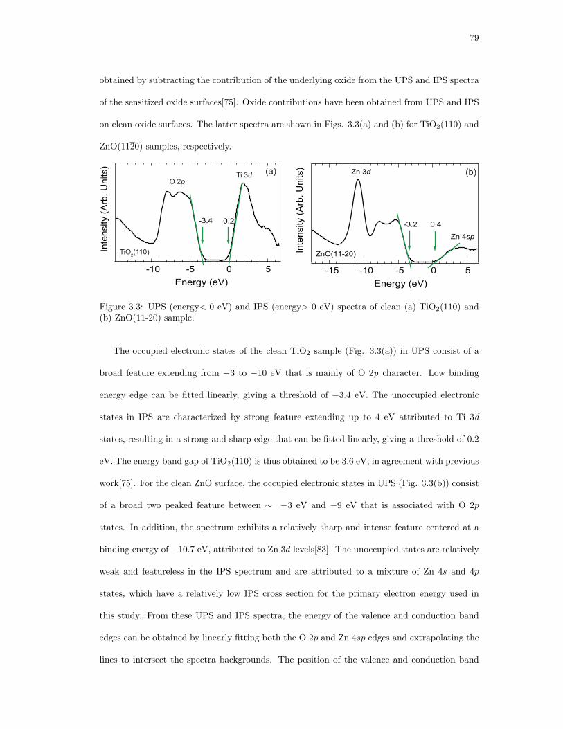
79
obtained by subtracting the contribution of the underlying oxide from the UPS and IPS spectra
of the sensitized oxide surfaces[75]. Oxide contributions have been obtained from UPS and IPS
on clean oxide surfaces. The latter spectra are shown in Figs. 3.3(a) and (b) for TiO2(110) and
ZnO(1120) samples, respectively.
Inte
nsity (
Arb
. U
nits)
-15 -10 -5 0 5
Energy (eV)
Zn 3d
-3.2 0.4
ZnO(11-20)
Zn 4sp
(a)O 2p
TiO2(110)
(b)Ti 3d
0.2-3.4
0 5-5-10
Energy (eV)
Inte
nsity (
Arb
. U
nits)
Figure 3.3: UPS (energy< 0 eV) and IPS (energy> 0 eV) spectra of clean (a) TiO2(110) and(b) ZnO(11-20) sample.
The occupied electronic states of the clean TiO2 sample (Fig. 3.3(a)) in UPS consist of a
broad feature extending from −3 to −10 eV that is mainly of O 2p character. Low binding
energy edge can be fitted linearly, giving a threshold of −3.4 eV. The unoccupied electronic
states in IPS are characterized by strong feature extending up to 4 eV attributed to Ti 3d
states, resulting in a strong and sharp edge that can be fitted linearly, giving a threshold of 0.2
eV. The energy band gap of TiO2(110) is thus obtained to be 3.6 eV, in agreement with previous
work[75]. For the clean ZnO surface, the occupied electronic states in UPS (Fig. 3.3(b)) consist
of a broad two peaked feature between ∼ −3 eV and −9 eV that is associated with O 2p
states. In addition, the spectrum exhibits a relatively sharp and intense feature centered at a
binding energy of −10.7 eV, attributed to Zn 3d levels[83]. The unoccupied states are relatively
weak and featureless in the IPS spectrum and are attributed to a mixture of Zn 4s and 4p
states, which have a relatively low IPS cross section for the primary electron energy used in
this study. From these UPS and IPS spectra, the energy of the valence and conduction band
edges can be obtained by linearly fitting both the O 2p and Zn 4sp edges and extrapolating the
lines to intersect the spectra backgrounds. The position of the valence and conduction band

80
edges are found at −3.2 eV and 0.4 eV, respectively, giving a band gap of 3.6 eV for the clean
ZnO(1120)[75]. These clean oxide spectra were scaled prior to subtraction from the spectra of
the dye-sensitized oxide samples, as shown as an example of ZnTPP-Ipa dye in Fig. 3.4. The
scaling factor was determined by removal of the substrate related features in the dye-sensitized
spectra. These features are: for the UPS spectra of the dye-sensitized ZnO, the Zn 3d feature
appearing as a shoulder in the spectra at ∼ −11 eV; for the IPS spectra of the dye-sensitized
TiO2 samples that was the Ti 4d feature appearing right at the Fermi level. Since the clean ZnO
IPS spectrum is low in intensity and the clean TiO2 UPS spectrum lacks any sharp features
readily detectable in sensitized spectra, it was hard to determine the right scaling factor for
these spectra. Therefore, the scaling factor used was similar to the one for the clean ZnO UPS
and the clean TiO2 IPS spectra, respectively.
Inte
nsity (
arb
. u
nits)
-15 -10 -5 0 5
Binding energy (eV)
ZnTPP-Ipa + TiO2
TiO2
ZnTPP-Ipa
Inte
nsity (
arb
. u
nits)
-15 -10 -5 0 5
Binding energy (eV)
ZnTPP-Ipa + ZnO ZnO ZnTPP-Ipa
(a) (b)
Figure 3.4: An example of the subtraction procedure and obtaining the ZnTPP-Ipa molecularcontribution to the UPS and IPS spectra for the molecules adsorbed on (a)TiO2(110) and (b)ZnO(11-20) surface.
A first glance at Figs. 3.5(a) and 3.5(b) suggests that on both surfaces a given molecule has
a very similar density of states. This can be better understood by comparing the experimental
results to the calculated DOS.
Calculated molecular DOSs modified as outlined in Section 2.9 of Chapter 2 are shown in Fig.
3.5(c). The resemblance between the calculated DOS and the respective measured counterpart
of the dyes chemisorbed onto the ZnO(1120) and TiO2(110) surfaces is striking. Keeping in
mind that the experimental cross section effects are not taken into account in the calculated
DOS shown in Fig. 3.5(c), the comparison of the ab-initio results to the measured occupied
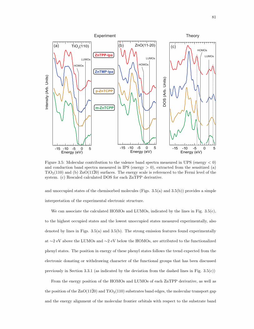
81
-15 -10 -5 0 5Energy (eV)
ZnO(11-20)In
ten
sity (
Arb
. U
nits)
-15 -10 -5 0 5Energy (eV)
TiO2(110)
DO
S (
Arb
. U
nits)
-15 -10 -5 0 5Energy (eV)
Experiment Theory
(a) (c)
HOMOs
LUMOs
HOMOs
LUMOs
HOMOs
LUMOsZnTPP-Ipa
ZnTMP-Ipa
p-ZnTCPP
m-ZnTCPP
(b)
Figure 3.5: Molecular contribution to the valence band spectra measured in UPS (energy < 0)and conduction band spectra measured in IPS (energy > 0), extracted from the sensitized (a)TiO2(110) and (b) ZnO(1120) surfaces. The energy scale is referenced to the Fermi level of thesystem. (c) Rescaled calculated DOS for each ZnTPP derivative.
and unoccupied states of the chemisorbed molecules (Figs. 3.5(a) and 3.5(b)) provides a simple
interpretation of the experimental electronic structure.
We can associate the calculated HOMOs and LUMOs, indicated by the lines in Fig. 3.5(c),
to the highest occupied states and the lowest unoccupied states measured experimentally, also
denoted by lines in Figs. 3.5(a) and 3.5(b). The strong emission features found experimentally
at ∼2 eV above the LUMOs and ∼2 eV below the HOMOs, are attributed to the functionalized
phenyl states. The position in energy of these phenyl states follows the trend expected from the
electronic donating or withdrawing character of the functional groups that has been discussed
previously in Section 3.3.1 (as indicated by the deviation from the dashed lines in Fig. 3.5(c))
From the energy position of the HOMOs and LUMOs of each ZnTPP derivative, as well as
the position of the ZnO(1120) and TiO2(110) substrates band edges, the molecular transport gap
and the energy alignment of the molecular frontier orbitals with respect to the substrate band
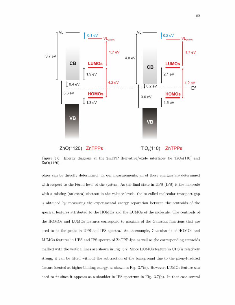
82
ZnO(11 0)2 TiO (110)2ZnTPPs ZnTPPs
CBCB
VBVB
Ef
1.9 eV 2.1 eV
1.3 eV
4.2 eV 4.2 eV
1.7 eV
0.2 eV0.1 eV
1.7 eV
1.5 eV
3.6 eV3.6 eV
4.0 eV3.7 eV
0.2 eV0.4 eV
HOMOs
LUMOs
HOMOs
LUMOs
VL VL
VLZnTPPs VLZnTPPs
Figure 3.6: Energy diagram at the ZnTPP derivative/oxide interfaces for TiO2(110) andZnO(1120).
edges can be directly determined. In our measurements, all of these energies are determined
with respect to the Fermi level of the system. As the final state in UPS (IPS) is the molecule
with a missing (an extra) electron in the valence levels, the so-called molecular transport gap
is obtained by measuring the experimental energy separation between the centroids of the
spectral features attributed to the HOMOs and the LUMOs of the molecule. The centroids of
the HOMOs and LUMOs features correspond to maxima of the Gaussian functions that are
used to fit the peaks in UPS and IPS spectra. As an example, Gaussian fit of HOMOs and
LUMOs features in UPS and IPS spectra of ZnTPP-Ipa as well as the corresponding centroids
marked with the vertical lines are shown in Fig. 3.7. Since HOMOs feature in UPS is relatively
strong, it can be fitted without the subtraction of the background due to the phenyl-related
feature located at higher binding energy, as shown in Fig. 3.7(a). However, LUMOs feature was
hard to fit since it appears as a shoulder in IPS spectrum in Fig. 3.7(b). In that case several
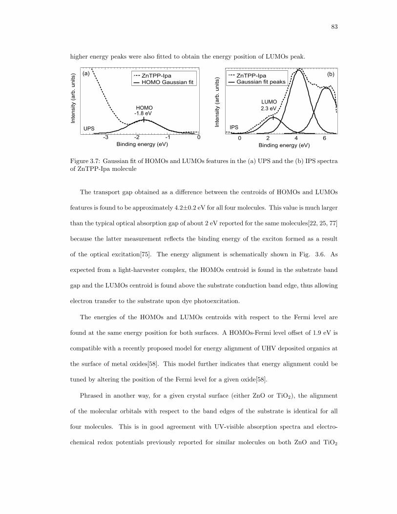
83
higher energy peaks were also fitted to obtain the energy position of LUMOs peak.
Inte
nsity (
arb
. u
nits)
6420
Binding energy (eV)
IPS
LUMO
2.3 eV
(b) ZnTPP-Ipa
HOMO Gaussian fit
HOMO-1.8 eV
ZnTPP-Ipa Gaussian fit peaks
UPS
(a)In
ten
sity (
arb
. u
nits)
-3 -2 -1 0
Binding energy (eV)
Figure 3.7: Gaussian fit of HOMOs and LUMOs features in the (a) UPS and the (b) IPS spectraof ZnTPP-Ipa molecule
The transport gap obtained as a difference between the centroids of HOMOs and LUMOs
features is found to be approximately 4.2±0.2 eV for all four molecules. This value is much larger
than the typical optical absorption gap of about 2 eV reported for the same molecules[22, 25, 77]
because the latter measurement reflects the binding energy of the exciton formed as a result
of the optical excitation[75]. The energy alignment is schematically shown in Fig. 3.6. As
expected from a light-harvester complex, the HOMOs centroid is found in the substrate band
gap and the LUMOs centroid is found above the substrate conduction band edge, thus allowing
electron transfer to the substrate upon dye photoexcitation.
The energies of the HOMOs and LUMOs centroids with respect to the Fermi level are
found at the same energy position for both surfaces. A HOMOs-Fermi level offset of 1.9 eV is
compatible with a recently proposed model for energy alignment of UHV deposited organics at
the surface of metal oxides[58]. This model further indicates that energy alignment could be
tuned by altering the position of the Fermi level for a given oxide[58].
Phrased in another way, for a given crystal surface (either ZnO or TiO2), the alignment
of the molecular orbitals with respect to the band edges of the substrate is identical for all
four molecules. This is in good agreement with UV-visible absorption spectra and electro-
chemical redox potentials previously reported for similar molecules on both ZnO and TiO2

84
nanoparticles[22, 25, 77], and is consistent with the frontier orbitals being essentially indepen-
dent of the phenyl functionalization.
In contrast, however, the relative energy alignment of the ZnTPP frontier orbitals with re-
spect to the oxides band edges is consistently∼ 0.2 eV different on the TiO2(110) and ZnO(1120)
surfaces. For example, for ZnTMP-Ipa the centroid of the HOMOs is found 1.3 eV above the
valence band of TiO2(110) and 1.5 eV above the valence band of ZnO(1120). The LUMOs-
related feature is found 1.9 eV above the conduction band of TiO2(110) and 2.1 eV above the
conduction band of ZnO(1120). In other words, while the energy position of the HOMOs and
LUMOs of the ZnTPP derivatives (given in Table 3.2) are found at different offsets from the
conduction band and valence band edges of the respective substrates, they are at similar energy
position with respect to their common Fermi level.
Table 3.2: Position of HOMO-1/HOMO and LUMOs centroids extracted from the experimentalspectra measured on sensitized TiO2(110) and resulting energy gap. All energies are given ineV and referenced with respect to the Fermi level of the system.
Molecule E(HOMOs) E(LUMOs) Eg
ZnTPP-Ipa −1.8± 0.1 2.3± 0.1 4.1± 0.2
ZnTMP-Ipa −1.9± 0.1 2.3± 0.1 4.2± 0.2
p-ZnTCPP −1.9± 0.1 2.3± 0.1[84] 4.2± 0.2[84]
m-ZnTCPP −1.9± 0.1 2.3± 0.1[84] 4.2± 0.2[84]
3.3.2 Adsorption geometry
Molecular orientation
The results presented in the previous section show that the electronic structures of the four
ZnTPP derivatives are nearly identical to each other. Yet when adsorbed on the wide band gap
oxides, their optical absorption spectra and performance in device configurations differ consider-
ably. This suggests that the surface adsorption geometry of the molecule may play a key role in
generating mentioned differences. NEXAFS spectroscopy is a well-suited area-averaging probe
to understand the organization of chemisorbed adsorbates on ordered surfaces[73]. NEXAFS
involves photoexcitation of a core electron to the lowest-lying unoccupied states of the molecule.

85
Here, the former may be the C 1s or N 1s core level, and the latter are the LUMOs on the
porphyrin macrocycle or, at slightly higher energy, the π system of the phenyls. More details
about NEXAFS measurements and instrumentation can be found in Section 2.8. Since a core
electron is involved, the spectrum contains information local to the excited atom. The ZnTPP
derivatives possess four equivalent N sites, all on the porphyrin macrocycle. In principle, there
are five inequivalent C sites with different binding energies[85, 86], but energy splitting between
the core levels on these sites is sufficiently small and can be neglected. Thus both the line shapes
of the N 1s and C 1s edges are directly representative of the transitions to the the unoccupied
DOS at these sites. However, owing to the location of N and C atoms in these molecules (as
shown in Fig. 3.1), the N 1s edge spectra will be representative of the unoccupied states on
the central porphyrin ring, whereas the C 1s spectra will probe both the porphyrin and the
phenyl rings[85, 86]. Moreover, when the exciting radiation is linearly polarized, the intensity
of an absorption peak depends upon the angle between the photon polarization direction and
the orientation of the unoccupied orbitals into which the transition is made. For example, the
intensity of the NEXAFS transition associated with the LUMOs localized on the ZnP ring will
be maximized when the electric field vector of the incident light is parallel to the p orbitals
composing the π∗ system of the ZnP plane (θ=0) and nearly suppressed when the electric field
is perpendicular to the same p orbitals (θ=90). Thus, by monitoring the intensity changes,
or the so-called dichroism, of a spectral feature as a function of polarization orientation, the
orientation of the molecule with respect to the plane of the surface can be determined. Fur-
ther details about the orientation determination using angle-resolved NEXAFS can be found
in Appendix E. In order to study the adsorption geometry effects without the complication
of differing electronic structures, we have restricted our NEXAFS study to p-ZnTCPP and
m-ZnTCPP: the two ZnTPP derivatives that possess essentially the same DOS.
The crystalline surfaces used in this study both have two-fold symmetry. In these measure-
ments, the electric field of the polarized synchrotron light was aligned with either the [100] or
[110] crystallographic directions for TiO2(110) and with the [1000] or [1100] crystallographic

86
directions for ZnO(1120). The two-fold symmetry of the clean surfaces did not induce an az-
imuthal dichroism in the NEXAFS signal of the adsorbed species, i.e. there was no change in
the intensity of NEXAFS features when the samples were rotated by 90 around the surface
normal. Therefore, results for only one sample orientation will be shown here. NEXAFS spectra
have been recorded as a function of the angle θ between the polarization vector of the incident
photons and the surface normal.
NE
XA
FS
in
ten
sity (
Arb
. U
nits)
290288286284282
Photon energy (eV)
NE
XA
FS
in
ten
sity (
Arb
. U
nits)
408404400396
Photon energy (eV)
NE
XA
FS
in
ten
sity (
Arb
. U
nits)
290288286284282Photon energy (eV)
NE
XA
FS
in
ten
sity (
Arb
. U
nits)
408404400396Photon energy (eV)
θ=20o
θ=30o
θ=55o
θ=70o
θ=80o
θ=90o
θ=20o
θ=30o
θ=55o
θ=70o
θ=80o
θ=90o
θ=20o
θ=30o
θ=55o
θ=70o
θ=80o
θ=90o
θ=20o
θ=30o
θ=55o
θ=70o
θ=80o
θ=90o
(a) (b) (c) (d)C1s C1sN1s N1s
LUMOs
PhLUMOs
Ph
TiO2(110) ZnO(11-20)
m-ZnTCPP
E
hνE
θ=0o
(e)
n
E
hν
θ=90o
Figure 3.8: NEXAFS spectra of the m-ZnTCPP molecule adsorbed onto TiO2(110) andZnO(1120) at the C 1s (a) and (c) and the N 1s (b) and (d) edges as a function of the lightincidence angle θ. The electric field is aligned with the [100] crystallographic direction for theTiO2(110) surface, and with the [1000] direction for the ZnO(1120) surface.
Figure 3.8 shows the angle-dependant NEXAFS spectra of the C 1s and N 1s edges, measured
from m-ZnTCPP-functionalized TiO2(110) and ZnO(1120) surfaces. At the C 1s edge, the
threshold feature at∼ 284 eV is attributed to transitions to the LUMOs located on the porphyrin
macrocycle, while the feature at ∼ 285 eV is attributed to transition to the unoccupied phenyl
states. For both surfaces, the intensity of the LUMOs feature decreases with increasing the
87
angle between the photon polarization vector and the surface normal (as shown in Figs. 3.8
(a) and (c)). In contrast, the intense phenyl feature at ∼ 285 eV does not display a strong
dichroic behavior. At the N 1s edge (Figs. 3.8 (b) and (d)), a strong dichroism is observed and
the intensities of all transitions are reduced as the photon polarization vector nears alignment
with the surface. This nature of the dichroism exhibited in both the C 1s and N 1s spectra
indicates that m-ZnTCPP adsorbs with the porphyrin macrocycle parallel to the oxide surface
for both crystals (as shown schematically in Fig. 3.8(e)). The lack of dichroism of the ∼ 285
eV feature of the C 1s spectrum can be attributed to either: i) a small tilt angle between the
phenyls and the ZnP ring upon adsorption; and/or ii) near cancelation of the dichroism from
orbitals on the the phenyl rings, which lie nearly perpendicular to the surface, and those on
the ZnP ring which lie parallel to the surface[87]. The NEXAFS spectra measured on the same
surfaces sensitized with the p-ZnTCPP molecules are, however, markedly different from those
found for m-ZnTCPP, and indicate a very different adsorption geometry. The corresponding
angle-dependent NEXAFS spectra of C 1s and N 1s edges are shown in Figure 3.9. For both
surfaces, no dichroism is observed at the C 1s edge (Figs. 3.9 (a) and (c)) or at the N 1s edge
(Figs. 3.9 (b) and (d)). This can be interpreted either as a random orientation of the molecular
species at the surface, or as an adsorption geometry where the ZnP plane makes an angle close
to 55 (“magic angle”) with the surface of the sample. More about the “magic angle” can be
found in Appendix E. This latter case is illustrated in Fig. 3.9(e). Regardless of the detailed
geometry of p-ZnTCPP, it is clear that the two molecules bound to TiO2 and ZnO in radically
different ways.
Real-space images of m-ZnTCPP on TiO2(110)
A more direct method that can help us to gain a more detailed insight into the adsorption
geometry of the molecular adsorbates on surfaces is the real-space imaging of the system using
scanning tunnel microscopy (STM). Scanning tunneling microscopy images of the passivated
and m-ZnTCPP functionalized TiO2(110) surfaces, prepared as described in Section 3.2.3, are

88
θ=20o
θ=30o
θ=55o
θ=70o
θ=80o
θ=90o
θ=20o
θ=30o
θ=55o
θ=70o
θ=80o
θ=90o
θ=20o
θ=30o
θ=55o
θ=70o
θ=80o
θ=90o
(a) (b) (c) (d)C1s C1sN1s N1s
TiO2(110) ZnO(11-20)
E
hνE
θ=0o
(e)
n
E
hν
θ=90o
NE
XA
FS
in
ten
sity (
Arb
. U
nits)
290288286284282
Photon energy (eV)
NE
XA
FS
in
ten
sity (
Arb
. U
nits)
408404400396
Photon energy (eV)
NE
XA
FS
in
ten
sity (
Arb
. U
nits)
290288286284282Photon energy (eV)
NE
XA
FS
in
ten
sity (
Arb
. U
nits)
408404400396
Photon energy (eV)
θ=20o
θ=30o
θ=55o
θ=70o
θ=80o
θ=90o
p-ZnTCPP
Figure 3.9: NEXAFS spectra of p-ZnTCPP adsorbed onto TiO2(110) and ZnO(1120) at the C1s (a) and (c) and the N 1s (b) and (d) edges as a function of the light incidence angle θ. Theelectric field is aligned with the [100] crystallographic direction for the TiO2(110) surface, andwith the [1000] direction for the ZnO(1120) surface.
reported in Fig. 3.10. Figure 3.10(a) shows a close-up image of the ordered pivalate layer
formed onto the TiO2(110) surface before sensitization. The adsorbed pivalic acid molecules
are highlighted by green circles both on the STM image and in the schematic diagram of the
surface geometry presented in Fig. 3.10(d). Figure 3.10(c) shows a large-area image of the
passivated TiO2(110) after sensitization. The image is characterized by a regular array of small
bright dots, with the four-lobed clusters of brighter ovals interspersed. As indicated by the
white squares, the former structures are identified as ordered pivalate species still present on
the surface after sensitization. The newly present four-lobed features are interpreted as an
image of the empty phenyl states of m-ZnTCPP adsorbed with their central ZnP ring parallel
to the surface. Furthermore, it is apparent from Fig. 3.10(c), and the close-up image in Fig.
3.10(b), that m-ZnTCPP adsorbs at preferred binding sites, with a well defined orientation

89
with respect to the high symmetry directions of the surface, as well as with respect to each
other. A model for the adsorption of m-ZnTCPP, and the pivalate species, is presented in Fig.
3.10(d). We propose that m-ZnTCPP binds to every other exposed 5-fold coordinated Ti row
3.1Å
6.5 Å[1 0]1
[1 0]1
Pivalic acid
m-ZnTCPP
Ti
O
[001]
[110]
TiO (110)2
[001]
Pivalic acid patches
(c)
[001]
(b)
(a)
m-ZnTCPP
Top viewSide view(d)
Figure 3.10: (a) Unoccupied states measured in STM (U=1.6V, I=1nA) of an ordered pivalatelayer on a TiO2(110) surface before sensitization. (b) and (c) STM image of the surface sen-sitized with m-ZnTCPP in unoccupied states (U=2V, I=1nA). (d) Adsorption geometries ofboth the pivalate layer and the m-ZnTCPP molecules are proposed in the side view and topview schematics of a TiO2(110) surface.
at the surface through the carboxylate species in the meta position on the phenyl groups. The
porphyrin ring is parallel to the surface and the phenyl groups are essentially upright. The
close-up image in Fig. 3.10(b) suggests that the adjacent m-ZnTCPP molecules are offset by
one 5-fold Ti row, likely to reduce the repulsive interaction between the phenyl groups on the
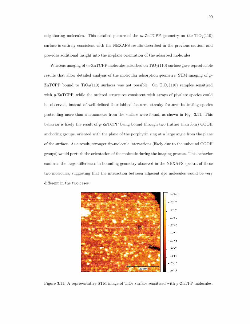
90
neighboring molecules. This detailed picture of the m-ZnTCPP geometry on the TiO2(110)
surface is entirely consistent with the NEXAFS results described in the previous section, and
provides additional insight into the in-plane orientation of the adsorbed molecules.
Whereas imaging of m-ZnTCPP molecules adsorbed on TiO2(110) surface gave reproducible
results that allow detailed analysis of the molecular adsorption geometry, STM imaging of p-
ZnTCPP bound to TiO2(110) surfaces was not possible. On TiO2(110) samples sensitized
with p-ZnTCPP, while the ordered structures consistent with arrays of pivalate species could
be observed, instead of well-defined four-lobbed features, streaky features indicating species
protruding more than a nanometer from the surface were found, as shown in Fig. 3.11. This
behavior is likely the result of p-ZnTCPP being bound through two (rather than four) COOH
anchoring groups, oriented with the plane of the porphyrin ring at a large angle from the plane
of the surface. As a result, stronger tip-molecule interactions (likely due to the unbound COOH
groups) would perturb the orientation of the molecule during the imaging process. This behavior
confirms the large differences in bounding geometry observed in the NEXAFS spectra of these
two molecules, suggesting that the interaction between adjacent dye molecules would be very
different in the two cases.
30 nm
Figure 3.11: A representative STM image of TiO2 surface sensitized with p-ZnTPP molecules.

91
Optical properties and exciton delocalization
Different adsorption geometries for m-ZnTCPP and p-ZnTCPP when bound to TiO2 can ex-
plain differences in the optical absorption properties found when TiO2 nanoparticles are sen-
sitized with these molecules. The UV-visible absorption spectra for these two cases are shown
in Fig. 3.12 (adapted from previous work)[22, 25]. The absorption spectrum of m-ZnTCPP
is characterized by a strong Soret (or B) band centered at 424 nm and weaker Q band with
features at 557 and 597 nm and is essentially identical to what is found for both m-ZnTCPP and
p-ZnTCPP in solution. In contrast, the Soret band of p-ZnTCPP exhibits a strong blue-shifted
component, generally attributed to H-aggregation: a face-to-face stacking of the excitation
dipoles that are aligned in the plane of ZnP macrocycle, as depicted in the lower inset of Fig.
3.12. The H-aggregation and its effects on the absorption spectrum are explained in more detail
in Appendix C. This sort of plane-to-plane coupling can occur only if the molecule is adsorbed
with the porphyrin ring at a large angle with respect to the plane of the surface, as we find for
p-ZnTCPP. In contrast, such intermolecular dipole-dipole interaction is absent for m-ZnTCPP
because their porphyrin macrocycles, and hence the optical dipoles, are parallel to the surface
(see upper inset in Fig. 3.12).
Figure 3.12: UV-visible absorption spectra measured on TiO2 nanoparticles sensitized with m-ZnTCPP and p-ZnTCPP. Adapted from [22, 25] The dipoles formed upon photoexcitation areindicated by green arrows in a schematic.
The measurements presented in this chapter provide a direct evidence that the position of the

92
COOH anchoring group on the phenyls of ZnTPP (either meta or para) controls the adsorption
geometry of the molecule on an oxide surface. The impact of the adsorption geometry on the
device performance is illustrated by the incident photon to current efficiency (IPCE) spectra,
defined in Section 1.2 of Chapter 1, for m-ZnTCPP and p-ZnTCPP molecules adsorbed on
TiO2 nanoparticles, as shown in Fig. 3.13(a). The details about these measurements can
be found elsewhere[22, 25]. It is clear that m-ZnTCPP-sensitized films exhibit a much larger
efficiency over the full spectrum when compared to films sensitized with p-ZnTCPP. As our
electronic structure measurements found essentially identical energy level offsets for these two
systems, the large difference in IPCE cannot be explained from a simple energy alignment
argument. Rather, the possible origin of the difference might be in the molecule-surface bonding
geometry. The upright geometry found for p-ZnTCPP allows neighboring molecules to have
parallel stacking of their porphyring macrocycles, opening a dipole-mediated intermolecular
electronic channel that competes with the direct injection of a photo-excited electron into the
TiO2 substrate, as illustrated in Fig. 3.13(c) and contributes significantly to the observed loss
of efficiency. However, there are other differences between the meta and the para molecules
that could influence the charge injection properties of the dye molecule and consequently IPCE
and efficiency of the DSSC. One such difference is that the meta molecules form four chemical
bonds with the oxide surface, whereas the para molecules form either one or two chemical
bonds. Furthermore, proximity of the molecule to the surface can also play a role in increasing
the charge injection. Because of their flat-lying binding geometry the LUMOs of the meta
molecule, are located closer to the surface of the oxide compared to the LUMOs of the para
molecule. It is expected that the electrons, excited into the LUMOs of the molecule by photon
absorption, are, thus more efficiently injected into the oxide conduction band from the meta
molecules compared to the para molecules.

93
(a)(c)
(b)
Figure 3.13: (a) Incident photon to current efficiency (IPCE) obtained from devices usingTiO2 nanoparticles sensitized with m-ZnTCPP and p-ZnCTPP (Adapted from [22, 25]) (b)Main de-excitation channel for a photoexcited m-ZnTCPP: electron injection into the substrateconduction band. (c) Additional de-excitation channel enabled by the stacked geometry of thep-ZnTCPP molecules: exciton delocalization through dipole-dipole interaction.
3.4 Conclusion
In this chapter we’ve presented a comprehensive approach to understand the problem of the
ZnTPP derivative-oxide interfaces that encompasses energy alignment, molecule-surface binding
geometry, molecular packing and their consequences on the electronic de-excitation pathways
of photoexcited electrons.
The electronic structure of the ZnTPP-Ipa, ZnTMP-Ipa, p-ZnTCPP and m-ZnTCPP mo-
lecules adsorbed both on TiO2(110) and ZnO(1120) surfaces, measured using UPS and IPS,
was interpreted using the gas phase molecular DOS calculations. The energy alignment of
the frontier orbitals relevant for the photoexcitation with respect to the substrate band edges
was directly extracted. The following conclusions about the energy level alignment have been
reached: i) On a given substrate, the energy alignment of the frontier orbitals of all four ZnTPP
derivatives considered in this study is identical. ii) The alignment of the ZnTPP derivatives
with respect to the TiO2 and ZnO band edges is shifted so as to keep the molecular levels at
the same position with respect to the substrate Fermi level.

94
In addition, the changes in the binding geometry due to different positions of COOH anchor-
ing group on the phenyl rings (either meta or para) have been studied. From NEXAFS spec-
troscopy, STM and UV-visible spectroscopy it has been found that the m-ZnTCPP molecule ad-
sorbs with its ZnP ring parallel to the oxide substrate surfaces, whereas the p-ZnTCPP molecule
adsorbs in a geometry where the ZnP ring is at a large angle from the surface plane (with a
possible tilt angle of ∼50 degrees.) In the case of m-ZnTCPP, the main de-excitation channel
for a photoexcited electron is expected to be through the injection into the substrate conduc-
tion band. On the contrary, the upward adsorption geometry of p-ZnTCPP allows face-to-face
stacking of the ZnP rings and thus opens a new de-excitation channel through dipole-dipole
interaction. Due to this additional de-excitation channel, the performance of the para dye in
the photovoltaic device is thus expected to be inferior compared to that of the meta dye, since
the number of electrons injected into the oxide substrate contributing to the photogenerated
current will be reduced.

95
Chapter 4
Electronic structure and energy level alignment of
free-base and zinc tetraphenylporphyrin molecules on
ZnO(1120)
4.1 Introduction
In the previous chapter we presented the study of the electronic structure, energy level alignment
and the adsorption geometry of four zinc(II)tetraphenylporphyrin derivatives chemisorbed on
ZnO and TiO2 surfaces. It was confirmed both with NEXAFS and STM measurements that the
m-ZnTPP and p-ZnTCPP molecules exhibit radically different adsorption geometries on the
oxide surfaces, with the m-ZnTPP molecule adsorbing flat with respect to the surface, while the
p-ZnTCPP molecules are essentially upright. The energy level alignment for all the molecules
was found insensitive to the binding geometry as well as the nature of the functional groups
located on the phenyl rings of the molecule.
In this chapter we will present a systematic study comparing the electronic structure of the
free-base and zinc tetracarboxyphenylporphyrin (TCPP) molecules adsorbed on the ZnO(1120)
single crystal surface. To explore the influence of both the central ion in the molecule and the
binding geometry on the electronic structure, four different derivatives, para and meta free-base
tetracarboxyphenylporphyrin (p-H2TCPP and m-H2TCPP) and para and meta zinc tetracar-
boxyphenylporphyrin (p-ZnTCPP and m-ZnTCPP) molecules (Figure 4.1(a)) were synthesized
and studied. Different central metal ions can be inserted into the porphyrin ring[9, 12, 88]. In
the majority of cases inserted metal ions have valence electrons in d orbitals. These orbitals,
in particular dπ (dxz and dyz) and dxy orbitals, can hybridized with porphyrin π molecular

96
orbitals granted these two orbitals are close in energy. The hybridization can lead to changes
in the electronic structure of the molecule, for example shifts of HOMOs and LUMOs of the
molecule, which can, in turn affects the optical properties of the molecule[81, 89]. The effect of
the presence of the central metal ion on both the occupied and unoccupied molecular states of
the selected TPP derivatives have been studied by comparing molecules with and without the
central zinc ion in the porphyrin ring. The binding geometry of the molecules can be controlled,
as shown in the study presented in Chapter 3, by attaching the carboxylic binding groups to
either para or meta positions on the four phenyl rings of the molecule. It is thus expected
that the para molecules in the study bind upright while the meta molecules bind flat to the
oxide surface (Figure 4.1c). Furthermore, the molecule-molecule interaction is also expected to
be influenced by the binding geometry of the molecules at the surface. Possible effects of the
molecule-molecule interaction on the electronic structure of the adsorbed molecules have also
been carefully examined in this chapter. All four types of molecules have been synthesized by
our collaborators at Elena Galoppini’s group from Chemistry Department at Rutgers University,
Newark.
Although the electronic structure of metalloporphyrins has been extensively studied exper-
imentally in solution using UV-vis absorption spectroscopy and electrochemical techniques or
in gas phase or thin films using UV photoemission, there is considerable scattering for the en-
ergies assigned to the frontier orbitals of these molecules. For example, a comparative UPS
study of gas phase ionization potentials (IPs) of several metallo-TPPs done by Khandelwal and
Roebber[90] suggests that the first IPs are all clustered in an energy range of 6.4±0.1 eV. More
specifically, the first IPs of the ZnTPP and the free-base TPP were found at 6.42 and 6.39 eV,
respectively. This conclusion was also reached through theoretical work done by Hashimoto et
al[91]. as well as experimental studies that include electrochemical measurements[88] and UPS
measurements on thin films of free-base and ZnTPP molecules[92]. On the other hand, signifi-
cant differences (larger than 0.3 eV) were reported between the HOMO levels of the free-base
TPP molecule and that of the ZnTPP molecule in the theoretical work by Piet et al.[93], as well
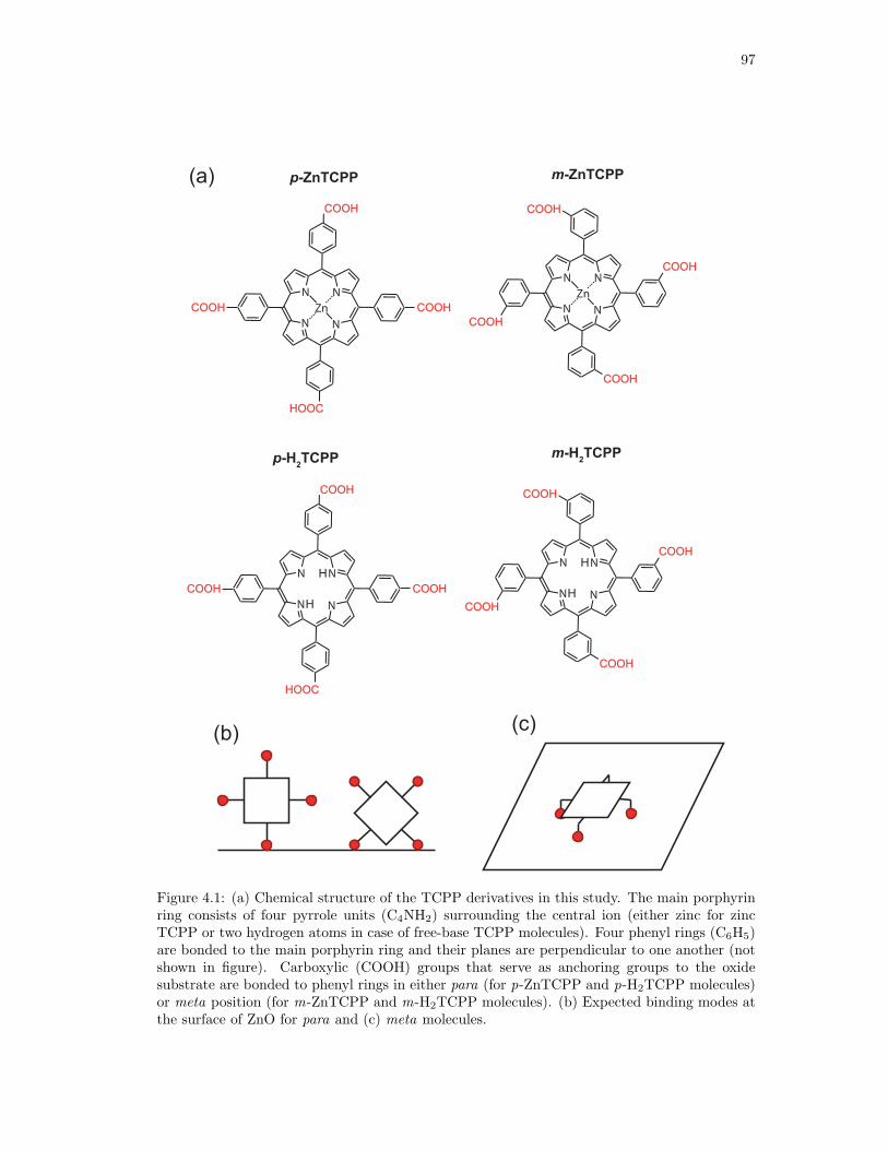
97
COOH
Zn
NN
N N
COOH
COOH
COOH
COOH
NN
N N
COOH
COOH
COOH
H
H
m-ZnTCPP
m-H2TCPP
COOH
Zn
NN
N N
COOH
HOOC
COOH
COOH
NN
N N
COOH
HOOC
COOH
H
H
p-ZnTCPP
p-H2TCPP
(a)
(b) (c)
Figure 4.1: (a) Chemical structure of the TCPP derivatives in this study. The main porphyrinring consists of four pyrrole units (C4NH2) surrounding the central ion (either zinc for zincTCPP or two hydrogen atoms in case of free-base TCPP molecules). Four phenyl rings (C6H5)are bonded to the main porphyrin ring and their planes are perpendicular to one another (notshown in figure). Carboxylic (COOH) groups that serve as anchoring groups to the oxidesubstrate are bonded to phenyl rings in either para (for p-ZnTCPP and p-H2TCPP molecules)or meta position (for m-ZnTCPP and m-H2TCPP molecules). (b) Expected binding modes atthe surface of ZnO for para and (c) meta molecules.

98
as from electrochemical measurements[94] and low-energy electron emission measurements[95].
Moreover, for metalloporphyrins chemisorbed onto a wide band gap semiconductor oxide such
as TiO2 or ZnO, little is known about the alignment of theses frontier orbitals with respect
to the substrate band edges. Anchoring of TPPs to TiO2 and ZnO can be achieved through
carboxylic acid functionalization of the phenyl groups, leading to chelating and/or bidentate
bridging of the carboxylate on the surface[9, 70, 96]. Oxidation potentials have been measured
more systematically for several ZnTPPs adsorbed onto ZnO nanoparticles indicating little vari-
ation between ZnTPP molecules with different functional groups located on the phenyl rings of
the molecule[22, 25]. Additional complications of the electronic structure arise on a saturated
surface from intermolecular effects. It has recently been shown that the adsorption geometry of
some ZnTPPs on a surface could dramatically modify the optical absorption properties due to
aggregation effects[13, 25].
Using a combination of X-ray and ultraviolet photoemission spectroscopy (XPS and UPS)
and inverse photoemission spectroscopy (IPS) in a single ultra-high vacuum (UHV) chamber,
the occupied and unoccupied electronic states of the four TCPPs chemisorbed onto the surface
of a ZnO(1120) single crystal have been measured. Since the UPS and IPS spectra are found
similar to the calculated DOS of the gas phase molecules, the frontier molecular orbitals in the
spectra were identified and their energy level alignment with respect to the band edges of the
ZnO substrate was extracted[75]. However, it is found that the related excited states of the
molecules, measured using ultraviolet-visible (UV-vis) absorption spectroscopy performed on
sensitized ZnO nanoparticles, are critical in order to distinguish the effects of the central metal
ion and the molecular interaction on the electronic structure.
99
4.2 Experimental Methods and Sample Preparation
4.2.1 Ultraviolet-visible absorption spectroscopy
Free-base and zinc tetracarboxyphenylporphyrin molecules were synthesized according to the
procedure reported earlier[25]. UV-Vis absorption spectra of free-base and zinc tetracarboxy-
phenylporphyrin molecules were acquired in transmission at ambient temperature in methanol
(Pharmco, HPLC-UV grade) using a dual-beam VARIAN Cary-500 Scan UV-Vis-NIR spec-
trophotometer. The details of the absorption spectroscopy instrumentation are given in Section
2.6 of Chapter 2. The sensitized ZnO mesoporous thin films were placed in a 1 cm quartz
cuvette in air while recording the spectra.
4.2.2 Ultraviolet, X-ray and inverse photoemission spectroscopies
X-ray, ultraviolet and inverse photoemission spectroscopies (XPS, UPS and IPS) were performed
in a single ultra-high vacuum (UHV) experimental chamber. The details of the spectroscopic
measurements and instrumentation can be found in Section 2.3 of Chapter 2. In the photoemis-
sion and inverse photoemission spectra, the valence band maximum (VBM) and the conduction
band minimum (CBM) are both measured with respect to the Fermi level of a gold sample
in contact with the oxide substrate. The overall instrumental resolution for UPS and IPS is
estimated to be 0.3 and 0.6 eV, respectively. The IPS measurements presented here have been
taken while keeping a small sample current (0.5 - 1 µA) for a beam size of 1 mm2 and by
sampling several spots on a large 1 cm2 sample with short beam exposure (3 - 10 min). For
such electron doses, no beam damage was observed during IPS nor in subsequent UPS and XPS
spectra.
The zinc oxide single crystal, cut and polished within 0.5 of the (1120) plane, was purchased
from MTI corporation. The crystal was degassed and prepared in UHV through several cycles
of 1 keV Ar+ ion sputtering (while maintaining a maximum sample current of 2 µA) and
annealing in UHV at 800 K. The cleanliness of the surface was checked using XPS. The single
100
crystal surface was subsequently sensitized ex-situ for 20 minutes in a solution of dye dissolved
in tetrahydrofuran (THF). After sensitization, the sample was rinsed with THF to prevent dye
accumulation, and reintroduced into the UHV analysis chamber.
4.3 Computational Methods
Electronic structure calculations, the details of which can be found in Section 2.9, were per-
formed using GAMESS(US)[74] software package. All calculations were carried out with a
restricted C2v symmetry for the free-base molecules and with a C4v symmetry for the zinc
containing molecules. Geometries in the local minima on the potential energy surface were cal-
culated using the 6-31G** polarization basis set[97, 98]. The density of states of the molecules
in the gas phase was obtained by a convolution of the resulting electronic states distribution
with a 1.2 eV full width at half maximum Gaussian function. This particular Gaussian width
was chosen because it best “simulated” the experimental broadening of the electronic states
which made the comparison with the experimental UPS and IPS spectra easier.
4.4 Results and discussion
4.4.1 UV-visible absorption spectra
UV-visible absorption spectroscopy has long been the technique of choice to probe the electronic
structure of porphyrins and their derivatives, and as such optical transitions of these molecules
have been extensively studied experimentally and theoretically[10, 21, 91, 99–105]. The opti-
cal absorption properties of free-base and zinc tetraphenylporphyrins and their derivatives are
closely related to those of porphyrins and zinc porphyrins. This is because the four phenyl rings
in the molecule lie perpendicular to the porphyrin macrocycle and as a result, π systems of the
phenyls and the macrocycle are essentially electronically decoupled. Detailed description of the
origin and the nomenclature of the features appearing in the UV-visible absorption spectrum
of porphyrins can be found in Section 2.6. Briefly, in general, UV-visible absorption spectrum

101
of porphyrins consists of two bands, an intense Soret band appearing in region of wavelengths
close to ultraviolet and much weaker Q band appearing in the optical region of wavelengths.
Spectrum of porphyrins is generally well understood in terms of the Gouterman four orbital
model, the details of which can be found in Appendix D. This model takes into account four
molecular frontier orbitals, the two almost degenerate HOMOs and the two almost degenerate
LUMOs and the transitions between them. The configuration interaction mixes the excited
states of the molecule causing the transitions to lower energy excited state to be highly sup-
pressed compared to the transitions to the higher excited state. Transitions to the lower energy
excited states are ascribed to Q band, while the transitions to higher energy excited states are
ascribed the the intense Soret band in the UV-visible spectrum of the porphyrins.
Owing to the weak electronic coupling between the porphyrin macrocycle and four phenyl
groups, adding functional groups to the phenyls is not expected to have a significant impact
on the optical absorption of the molecule. Thus, the TCPP derivatives present an interesting
case where, through a judicious choice of phenyl functional groups, the molecular adsorption
geometry on a surface and molecule/molecule interaction can be in principle modified without
appreciably altering its optical absorption or primary electrochemical properties.
To identify and characterize the m-H2TCPP, m-ZnTCPP, p-H2TCPP and p-ZnTCPP
molecules that were synthesized for this study, UV-visible absorption spectra of the molecules
in methanol or bonded to a ZnO nanoparticles thin film were obtained. These spectra are
presented in Fig. 4.2 and Fig. 4.3, respectively. The spectra measured for the m-ZnTCPP
and p-ZnTCPP molecules shown in Fig. 4.2(a) are quite similar and characterized by a Soret
band at 425 nm as well as by a typical two band Q region (at 557 nm and 596 nm for m-
ZnTCPP and 559 nm and 598 nm for p-ZnTCPP molecule). The free-base m-H2TCPP and
p-H2TCPP molecules exhibit in their absorption spectra shown in Fig. 4.2(b), a strong Soret
band at 416 nm as well as a characteristic four components Q band (at 515 nm, 551 nm, 590
nm, 644 nm for m-H−2TCPP and at 514 nm, 549 nm, 591 nm and 645 nm for p-H2TCPP
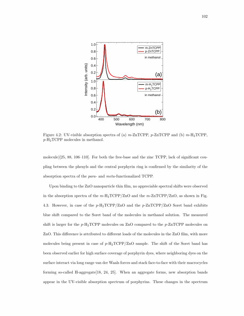
102
1.0
0.8
0.6
0.4
0.2
Inte
nsity
(ar
b. u
nits
)
800700600500400
Wavelength (nm)
1.0
0.8
0.6
0.4
0.2
0.0
m-ZnTCPP p-ZnTCPP
in methanol
(a)
m-H2TCPP p-H2TCPP
(b)
in methanol
Figure 4.2: UV-visible absorption spectra of (a) m-ZnTCPP, p-ZnTCPP and (b) m-H2TCPP,p-H2TCPP molecules in methanol.
molecule)[25, 88, 106–110]. For both the free-base and the zinc TCPP, lack of significant cou-
pling between the phenyls and the central porphyrin ring is confirmed by the similarity of the
absorption spectra of the para- and meta-functionalized TCPP.
Upon binding to the ZnO nanoparticle thin film, no appreciable spectral shifts were observed
in the absorption spectra of the m-H2TCPP/ZnO and the m-ZnTCPP/ZnO, as shown in Fig.
4.3. However, in case of the p-H2TCPP/ZnO and the p-ZnTCPP/ZnO Soret band exhibits
blue shift compared to the Soret band of the molecules in methanol solution. The measured
shift is larger for the p-H2TCPP molecules on ZnO compared to the p-ZnTCPP molecules on
ZnO. This difference is attributed to different loads of the molecules in the ZnO film, with more
molecules being present in case of p-H2TCPP/ZnO sample. The shift of the Soret band has
been observed earlier for high surface coverage of porphyrin dyes, where neighboring dyes on the
surface interact via long range van der Waals forces and stack face-to-face with their macrocycles
forming so-called H-aggregate[18, 24, 25]. When an aggregate forms, new absorption bands
appear in the UV-visible absorption spectrum of porphyrins. These changes in the spectrum
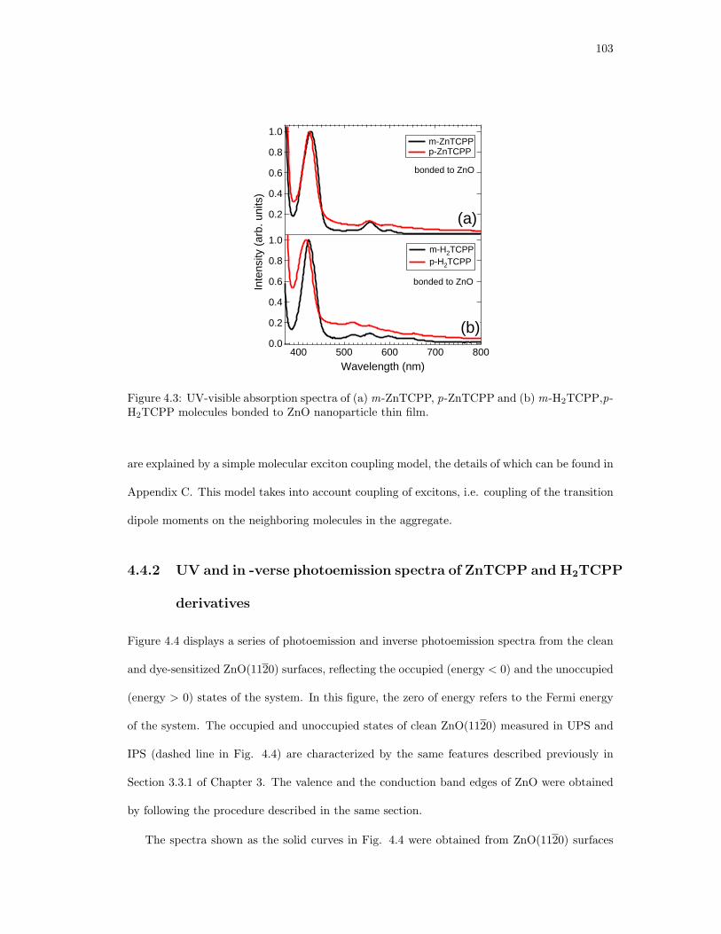
103
1.0
0.8
0.6
0.4
0.2
Inte
nsity
(ar
b. u
nits
)
800700600500400
Wavelength (nm)
1.0
0.8
0.6
0.4
0.2
0.0
m-ZnTCPP p-ZnTCPP
m-H2TCPP p-H2TCPP
(a)
(b)
bonded to ZnO
bonded to ZnO
Figure 4.3: UV-visible absorption spectra of (a) m-ZnTCPP, p-ZnTCPP and (b) m-H2TCPP,p-H2TCPP molecules bonded to ZnO nanoparticle thin film.
are explained by a simple molecular exciton coupling model, the details of which can be found in
Appendix C. This model takes into account coupling of excitons, i.e. coupling of the transition
dipole moments on the neighboring molecules in the aggregate.
4.4.2 UV and in -verse photoemission spectra of ZnTCPP and H2TCPP
derivatives
Figure 4.4 displays a series of photoemission and inverse photoemission spectra from the clean
and dye-sensitized ZnO(1120) surfaces, reflecting the occupied (energy < 0) and the unoccupied
(energy > 0) states of the system. In this figure, the zero of energy refers to the Fermi energy
of the system. The occupied and unoccupied states of clean ZnO(1120) measured in UPS and
IPS (dashed line in Fig. 4.4) are characterized by the same features described previously in
Section 3.3.1 of Chapter 3. The valence and the conduction band edges of ZnO were obtained
by following the procedure described in the same section.
The spectra shown as the solid curves in Fig. 4.4 were obtained from ZnO(1120) surfaces
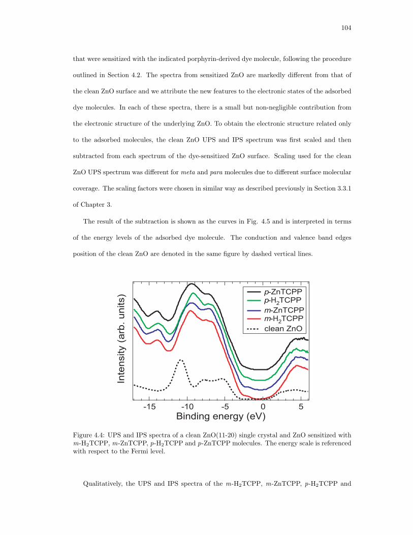
104
that were sensitized with the indicated porphyrin-derived dye molecule, following the procedure
outlined in Section 4.2. The spectra from sensitized ZnO are markedly different from that of
the clean ZnO surface and we attribute the new features to the electronic states of the adsorbed
dye molecules. In each of these spectra, there is a small but non-negligible contribution from
the electronic structure of the underlying ZnO. To obtain the electronic structure related only
to the adsorbed molecules, the clean ZnO UPS and IPS spectrum was first scaled and then
subtracted from each spectrum of the dye-sensitized ZnO surface. Scaling used for the clean
ZnO UPS spectrum was different for meta and para molecules due to different surface molecular
coverage. The scaling factors were chosen in similar way as described previously in Section 3.3.1
of Chapter 3.
The result of the subtraction is shown as the curves in Fig. 4.5 and is interpreted in terms
of the energy levels of the adsorbed dye molecule. The conduction and valence band edges
position of the clean ZnO are denoted in the same figure by dashed vertical lines.
Inte
nsity (
arb
. u
nits)
-15 -10 -5 0 5
Binding energy (eV)
p-ZnTCPP p-H2TCPP
m-ZnTCPP m-H2TCPP
clean ZnO
Figure 4.4: UPS and IPS spectra of a clean ZnO(11-20) single crystal and ZnO sensitized withm-H2TCPP, m-ZnTCPP, p-H2TCPP and p-ZnTCPP molecules. The energy scale is referencedwith respect to the Fermi level.
Qualitatively, the UPS and IPS spectra of the m-H2TCPP, m-ZnTCPP, p-H2TCPP and
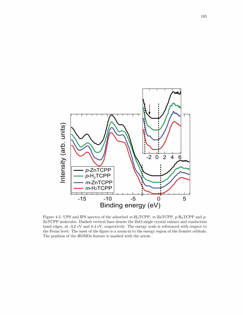
105
Inte
nsity (
arb
. u
nits)
-15 -10 -5 0 5
Binding energy (eV)
p-ZnTCPP p-H
2TCPP
m-ZnTCPP m-H2TCPP
6420-2
Figure 4.5: UPS and IPS spectra of the adsorbed m-H2TCPP, m-ZnTCPP, p-H2TCPP and p-ZnTCPP molecules. Dashed vertical lines denote the ZnO single crystal valence and conductionband edges, at -3.2 eV and 0.4 eV, respectively. The energy scale is referenced with respect tothe Fermi level. The inset of the figure is a zoom-in to the energy region of the frontier orbitals.The position of the HOMOs feature is marked with the arrow.

106
p-ZnTCPP molecules presented Fig. 4.5 are quite similar. The occupied electronic states that
are closest to the Fermi level are found inside of the ZnO band gap at a binding energy of
about −2 eV, as shown in the inset of Fig. 4.5. At higher binding energy, a series of molecular
structures are observed: a shoulder around −3.5 eV is visible on the rising slope of a multiple
component feature stretching from −5 to −11 eV, and a sharper peak is centered at around
−14 eV. In the unoccupied states, the IPS spectra appear rather featureless and are composed
of a main broad maximum at ∼ 4.5 eV, as shown in the inset of Fig. 4.5. The TPPs with
or without a central Zn ion have essentially the same UPS and IPS spectra. Note that no
spectral features attributable to Zn 3d levels are observed in the UPS spectra, due to the low
cross section of the Zn 3d states at this photon energy[111]. More importantly, although UV-vis
absorption spectra indicate the difference between para and meta molecules attributable to the
upright absorption geometry and aggregation effects found for para molecules, no appreciable
differences are observed in the UPS and IPS spectra.
4.4.3 Calculated molecular geometries and electronic structure of ZnTCPP
and H2TCPP derivatives
To facilitate the understanding of the UPS and IPS spectra, particularly given the broad energy
range experimentally accessible, DOS calculations were performed, enabling a direct comparison
with occupied and unoccupied measured molecular states.
Optimized geometries
For tetrapyrroles1 in general, it has been shown that theories which include electron corre-
lation effects, as does DFT, are superior to Hartree-Fock methods for geometry optimization
and ionization potentials calculation[112]. In particular, the B3LYP exchange-correlation func-
tional is well suited for TPP molecules[21, 75, 100, 113, 114].. As a part of the electronic
1Tetrapyrroles are a class of molecules that contain four pyrrole rings. Pyrrole is a cyclic aromatic compoundwith a ring consisting of four carbon atoms and one nitrogen atom. To form a tetrapyrrole, pyrrole rings aremost often interconnected through one carbon bridge either in linear or cyclic fashion. All porphyrin derivativesbelong to this class of molecules.

107
structure calculations, we performed geometry optimization to find the equilibrium geometry
of the molecules and to compare it to the results of the similar calculations that are already
available in the literature. For both the free-base and the zinc TCPP molecules, optimized
respectively in the C2v and in the C4v symmetries, the porphyrin macrocycles were found to
be planar, with the outer phenyls rings perpendicular to the central macrocycle, in agreement
with previous work[21, 75, 81, 82]. The resulting geometries for the p-H2TCPP molecule and
the m-ZnTCPP molecule are shown in Fig. 4.6. The geometries were found to be relatively
insensitive to the basis set for the para-substituted TCPP. However for smaller basis sets, the
presence of carboxylic groups in the meta position seemed to destabilize the overall structure
by inducing a 45 tilt angle between the phenyls and the macrocycle as well as the rumpling of
the macrocycle. Including a polarization function (6-31G**) on all light atoms (Zn excepted)
suppressed these distortions.
p-H2TCPP m-ZnTCPP
Figure 4.6: Calculated geometries of the p-H2TCPP and the m-ZnTCPP molecules optimizedin the C4v and C2v symmetries, respectively.
Calculated molecular DOS
The electronic structure of the ZnTCPP and the H2TCPP calculated here is, as expected,
very similar to those reported in the earlier studies of porphyrins and tetraphenylporphyrins.
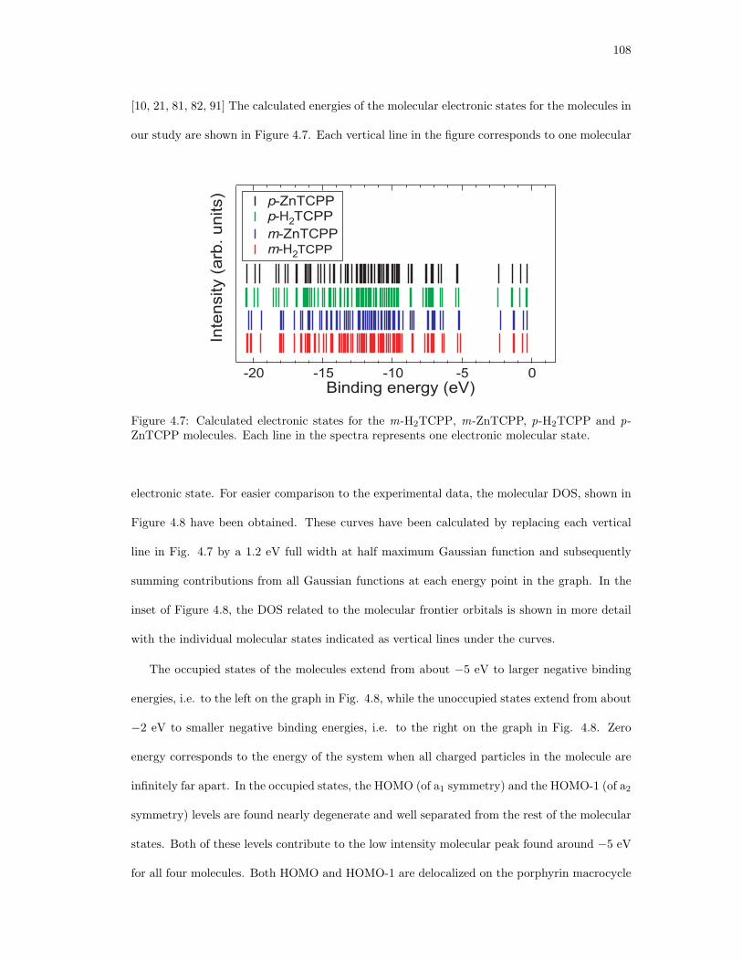
108
[10, 21, 81, 82, 91] The calculated energies of the molecular electronic states for the molecules in
our study are shown in Figure 4.7. Each vertical line in the figure corresponds to one molecular
Inte
nsity (
arb
. u
nits)
-20 -15 -10 -5 0Binding energy (eV)
p-ZnTCPP p-H2TCPP
m-ZnTCPP m-H2TCPP
Figure 4.7: Calculated electronic states for the m-H2TCPP, m-ZnTCPP, p-H2TCPP and p-ZnTCPP molecules. Each line in the spectra represents one electronic molecular state.
electronic state. For easier comparison to the experimental data, the molecular DOS, shown in
Figure 4.8 have been obtained. These curves have been calculated by replacing each vertical
line in Fig. 4.7 by a 1.2 eV full width at half maximum Gaussian function and subsequently
summing contributions from all Gaussian functions at each energy point in the graph. In the
inset of Figure 4.8, the DOS related to the molecular frontier orbitals is shown in more detail
with the individual molecular states indicated as vertical lines under the curves.
The occupied states of the molecules extend from about −5 eV to larger negative binding
energies, i.e. to the left on the graph in Fig. 4.8, while the unoccupied states extend from about
−2 eV to smaller negative binding energies, i.e. to the right on the graph in Fig. 4.8. Zero
energy corresponds to the energy of the system when all charged particles in the molecule are
infinitely far apart. In the occupied states, the HOMO (of a1 symmetry) and the HOMO-1 (of a2
symmetry) levels are found nearly degenerate and well separated from the rest of the molecular
states. Both of these levels contribute to the low intensity molecular peak found around −5 eV
for all four molecules. Both HOMO and HOMO-1 are delocalized on the porphyrin macrocycle
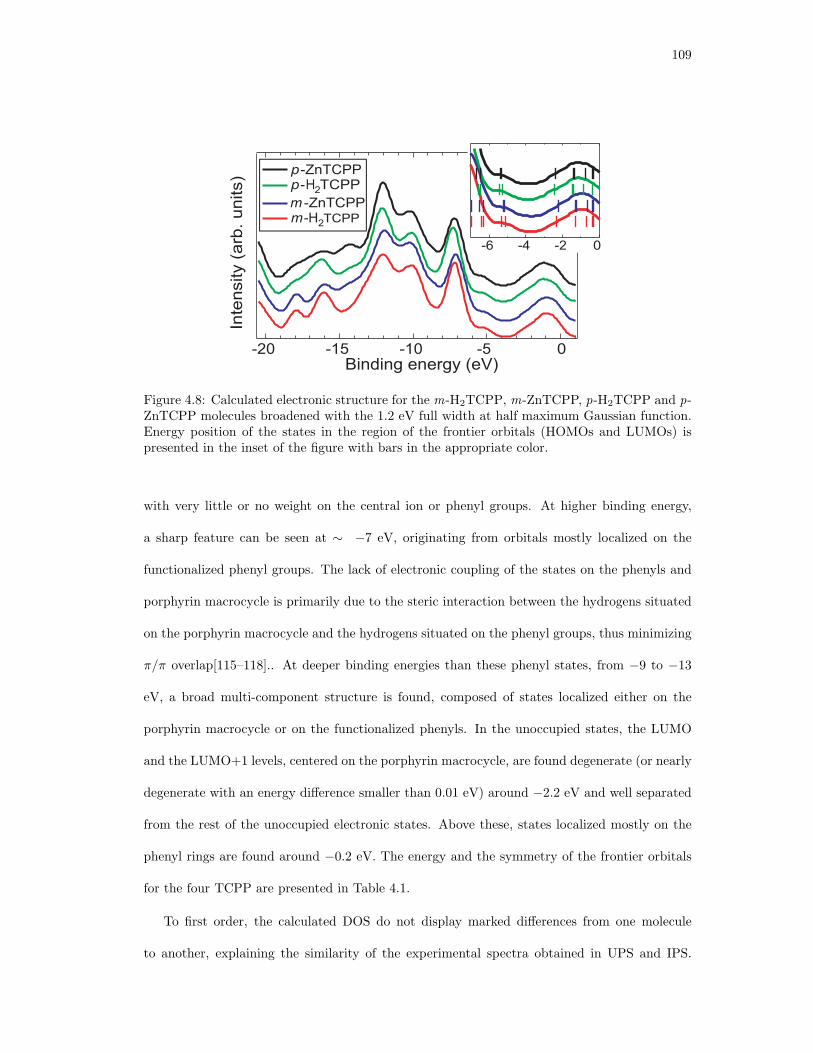
109
Inte
nsity (
arb
. units)
-20 -15 -10 -5 0Binding energy (eV)
p-ZnTCPP p-H2TCPP
m -ZnTCPP m-H2TCPP
-6 -4 -2 0
Figure 4.8: Calculated electronic structure for the m-H2TCPP, m-ZnTCPP, p-H2TCPP and p-ZnTCPP molecules broadened with the 1.2 eV full width at half maximum Gaussian function.Energy position of the states in the region of the frontier orbitals (HOMOs and LUMOs) ispresented in the inset of the figure with bars in the appropriate color.
with very little or no weight on the central ion or phenyl groups. At higher binding energy,
a sharp feature can be seen at ∼ −7 eV, originating from orbitals mostly localized on the
functionalized phenyl groups. The lack of electronic coupling of the states on the phenyls and
porphyrin macrocycle is primarily due to the steric interaction between the hydrogens situated
on the porphyrin macrocycle and the hydrogens situated on the phenyl groups, thus minimizing
π/π overlap[115–118].. At deeper binding energies than these phenyl states, from −9 to −13
eV, a broad multi-component structure is found, composed of states localized either on the
porphyrin macrocycle or on the functionalized phenyls. In the unoccupied states, the LUMO
and the LUMO+1 levels, centered on the porphyrin macrocycle, are found degenerate (or nearly
degenerate with an energy difference smaller than 0.01 eV) around −2.2 eV and well separated
from the rest of the unoccupied electronic states. Above these, states localized mostly on the
phenyl rings are found around −0.2 eV. The energy and the symmetry of the frontier orbitals
for the four TCPP are presented in Table 4.1.
To first order, the calculated DOS do not display marked differences from one molecule
to another, explaining the similarity of the experimental spectra obtained in UPS and IPS.
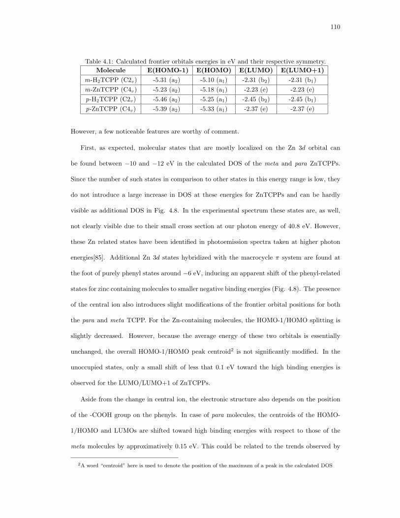
110
Table 4.1: Calculated frontier orbitals energies in eV and their respective symmetry.
Molecule E(HOMO-1) E(HOMO) E(LUMO) E(LUMO+1)
m-H2TCPP (C2v) -5.31 (a2) -5.10 (a1) -2.31 (b2) -2.31 (b1)
m-ZnTCPP (C4v) -5.23 (a2) -5.18 (a1) -2.23 (e) -2.23 (e)
p-H2TCPP (C2v) -5.46 (a2) -5.25 (a1) -2.45 (b2) -2.45 (b1)
p-ZnTCPP (C4v) -5.39 (a2) -5.33 (a1) -2.37 (e) -2.37 (e)
However, a few noticeable features are worthy of comment.
First, as expected, molecular states that are mostly localized on the Zn 3d orbital can
be found between −10 and −12 eV in the calculated DOS of the meta and para ZnTCPPs.
Since the number of such states in comparison to other states in this energy range is low, they
do not introduce a large increase in DOS at these energies for ZnTCPPs and can be hardly
visible as additional DOS in Fig. 4.8. In the experimental spectrum these states are, as well,
not clearly visible due to their small cross section at our photon energy of 40.8 eV. However,
these Zn related states have been identified in photoemission spectra taken at higher photon
energies[85]. Additional Zn 3d states hybridized with the macrocycle π system are found at
the foot of purely phenyl states around −6 eV, inducing an apparent shift of the phenyl-related
states for zinc containing molecules to smaller negative binding energies (Fig. 4.8). The presence
of the central ion also introduces slight modifications of the frontier orbital positions for both
the para and meta TCPP. For the Zn-containing molecules, the HOMO-1/HOMO splitting is
slightly decreased. However, because the average energy of these two orbitals is essentially
unchanged, the overall HOMO-1/HOMO peak centroid2 is not significantly modified. In the
unoccupied states, only a small shift of less that 0.1 eV toward the high binding energies is
observed for the LUMO/LUMO+1 of ZnTCPPs.
Aside from the change in central ion, the electronic structure also depends on the position
of the -COOH group on the phenyls. In case of para molecules, the centroids of the HOMO-
1/HOMO and LUMOs are shifted toward high binding energies with respect to those of the
meta molecules by approximatively 0.15 eV. This could be related to the trends observed by
2A word “centroid” here is used to denote the position of the maximum of a peak in the calculated DOS

111
Ghosh et al.[119], in which modifying the position of functional groups on the phenyls led to the
ionization potential variations. These variations are explained by the interaction between the
electric dipoles created by the presence of the either electron withdrawing or donating functional
groups on the phenyl rings and the charge density on the main porphyrin ring.
4.4.4 Comparison of calculated DOS and experi-mental UPS/IPS spec-
tra: Energy level alignment
A more detailed interpretation of the measured UPS and IPS spectra shown in Fig. 4.5 in
terms of the electronic structure is facilitated by a comparison to the ground state DOS shown
in Fig. 4.8. In principle only ∆Kohn-Sham energies, i.e. the energies of the fully relaxed
ionized molecular electronic states, should be directly compared to our experimental spectra.
However, information provided by the ground state DOS calculations has proven to be useful
for experimental data analysis on the same class of molecules[75].
Multiple similarities between the experimental spectra of the molecules chemisorbed on
the ZnO substrate and the calculated DOS for the molecules in the gas phase are a strong
indication that the molecule/surface interaction has only negligible effects on the resulting
electronic structure of the chemisorbed molecule. This is also confirmed by the similarity
between UPS measurements obtained earlier on a ZnTPP thin film[85] and our measurements
presented in this chapter.
It is now clear that the feature in the UPS spectra found at around −2 eV can be attributed
to the HOMO-1/HOMO levels. Interestingly, the intensity of this feature in the UPS spectra
seems to depend on the binding geometry of the molecules. Indeed, in case of the m-H2TCPP
and m-ZnTCPP, where the molecules are expected to bind with there ZnP macrocycle parallel
to the surface, the HOMO-1/HOMO feature is more intense than those of their para-substituted
equivalents, which are expected to bind upright at the oxide surface. This can be caused by the
upright adsorption geometry for the para molecules and “shadowing” of the molecules by each
other in the molecular layer adsorbed at the surface. In contrast, for meta molecules in flat-lying
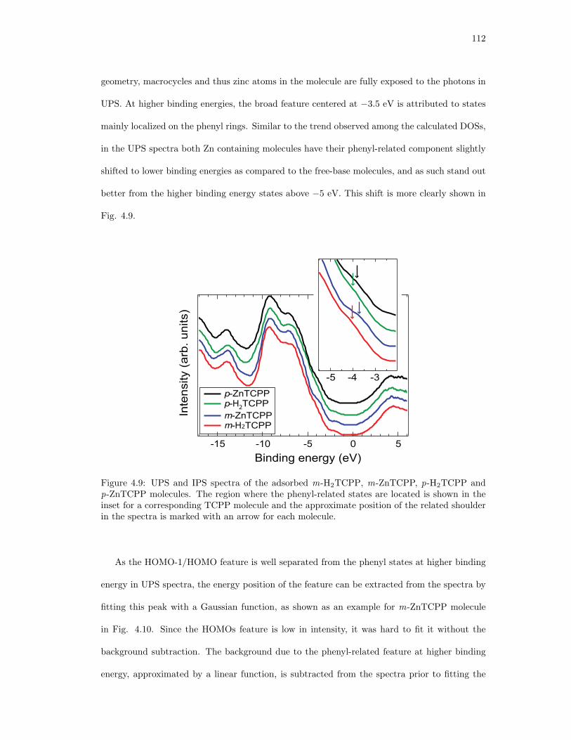
112
geometry, macrocycles and thus zinc atoms in the molecule are fully exposed to the photons in
UPS. At higher binding energies, the broad feature centered at −3.5 eV is attributed to states
mainly localized on the phenyl rings. Similar to the trend observed among the calculated DOSs,
in the UPS spectra both Zn containing molecules have their phenyl-related component slightly
shifted to lower binding energies as compared to the free-base molecules, and as such stand out
better from the higher binding energy states above −5 eV. This shift is more clearly shown in
Fig. 4.9.
Inte
nsity (
arb
. u
nits)
-15 -10 -5 0 5
Binding energy (eV)
p-ZnTCPP p-H
2TCPP
m-ZnTCPP m-H2TCPP
-5 -4 -3
Figure 4.9: UPS and IPS spectra of the adsorbed m-H2TCPP, m-ZnTCPP, p-H2TCPP andp-ZnTCPP molecules. The region where the phenyl-related states are located is shown in theinset for a corresponding TCPP molecule and the approximate position of the related shoulderin the spectra is marked with an arrow for each molecule.
As the HOMO-1/HOMO feature is well separated from the phenyl states at higher binding
energy in UPS spectra, the energy position of the feature can be extracted from the spectra by
fitting this peak with a Gaussian function, as shown as an example for m-ZnTCPP molecule
in Fig. 4.10. Since the HOMOs feature is low in intensity, it was hard to fit it without the
background subtraction. The background due to the phenyl-related feature at higher binding
energy, approximated by a linear function, is subtracted from the spectra prior to fitting the

113
HOMOs feature, as shown in the figure.
Inte
nsity (
arb
. u
nits)
Binding energy (eV)
m-ZnTCPP
HOMO Gaussian fit
UPS
HOMO-1.8 eV
-3.0 -2.5 -2.0 -1.5 -1.0
background
Figure 4.10: Gaussian fit of HOMO-1/HOMO feature in the UPS spectrum of m-ZnTCPPmolecule.
The resulting energy of the HOMO-1/HOMO centroid, i.e. the maximum of Gaussian
function used to fit the feature, is reported in Table 4.2 for all four molecules in the study. In
the unoccupied states, both the broadened calculated DOS and the IPS spectra are composed
of a single broad feature from which individual components cannot be isolated. In the previous
study that included the m-ZnTCPP dye, the results of which are presented in Section 3.3 of
Chapter 3, the position of the LUMO/LUMO+1 states was found to be +2.3±0.1 eV. This
was done by comparison of the m-ZnTCPP dye UPS spectrum with the UPS spectra of two
other ZnTPP derivatives for which the phenyl states were sufficiently separated in energy from
the LUMOs to allow a Gaussian fit[75]. Using the value of +2.3±0.1 eV for the centroid of
the LUMO/LUMO+1 states, a peak to peak energy gap is reported in Table 4.2 as the energy
difference between the centroid of the spectral features associated with the frontier orbitals for
each TCPP molecule. The energy gap obtained as the energy separation between the HOMOs
and the LUMOs feature in UPS and IPS reflects the so-called transport gap that is obtained
here to be ∼ 4.2 eV for all four molecules. The optical band gap, i.e. the energy it takes to
create an electron-hole pair, can be estimated from the Soret band energy position measured
in UV-visible absorption spectroscopy (Section 4.4.2) to be ∼2.9 eV. The transport gap is, as
114
expected, larger than the optical gap of the molecules. This difference is due to the exciton
binding energy, i.e. the energy it takes to separate the electron-hole pair. The exciton binding
energy for these molecules, obtained as the difference between the transport and the optical
band gaps, is 1.3 eV, which is in the expected energy range for the organic molecules[41].
As the position of the band edges of the ZnO(1120) substrate are known with respect to the
Fermi level, the energy alignment at the dye/surface interface can be directly measured and is
represented schematically in Fig. 4.11(b). For the m-ZnTCPP molecule, the centroid of the
HOMO-1/HOMO levels is found 1.4±0.1 eV above the valence band of ZnO, while the LUMOs
are found deep into the conduction band at 1.9±0.1 eV above the band edge. The energy level
alignment diagram for the same molecule chemisorbed on ZnO substrate was previously shown
in Chapter 3 and the HOMOs feature was found at 1.3 eV above the valence band maximum of
ZnO compared to 1.4 eV found in this study. However, these measurements were done on two
different m-ZnTCPP-sensitized samples and since the difference in the HOMOs peak position is
in the experimental uncertainty range of 0.1 eV, we interpret them as the variations induced by
different sample preparation conditions. Furthermore, similarity of the H2TCPP and ZnTCPP
molecular level alignment on ZnO found here is consistent with previous experiments indicating
similar electron injection properties for the free-base and Zn substitued molecules on TiO2[23].
There are no marked differences between the measured electronic structure of the meta
and the para molecules obtained in UPS and IPS. However, UV-vis absorption measurements
indicate the differences between themeta and the para molecules that can be explained by strong
aggregation effects for the upright-bonded para molecules. It is unclear if better instrumental
resolution in UPS and IPS would reveal aggregation effects in the electronic structure as the
UPS spectra presented in this chapter are similar to the results obtained with higher resolution
on more compact ZnTPP multilayers[85]. Possible aggregation effects have also no visible
influence on the energy alignment. However, it has been shown that DSSCs consisting of TiO2
nanoparticles sensitized with p-ZnTCPP resulted in worse photocurrents than those prepared
with m-ZnTCPP molecules[25]. In case of the ZnTPP derivatives, it is thus possible that the

115
limiting factor for dye performance is not the energy alignment of its molecular levels with
respect to the substrate band edges, but rather the π/π stacking that opens a delocalization
path for the exciton created upon the light absorption.
ZnO m-ZnTCPP
3.6 eV
1.9 eV
1.4 eV
LUMOs
HOMOs
CB
VB
ba
Inte
nsity (
arb
. u
nits)
-15 -10 -5 0 5
Binding energy (eV)
experimental spectrum
theoreticalspectrum
4.4
2.3-1.8
-3.6
-7.0-9.1
Ef
0.4 eV
1.8 eV
2.3 eV
Ef
Figure 4.11: (a) Comparison of the experimental occupied and unoccupied states of the m-ZnTCPP molecule compared to its gas phase calculated DOS. The position of major peaks inthe spectra are denoted on the experimental spectra (in eV). The ZnO(1120) surface band edgesare indicated by vertical lines. (b) Energy level alignment between the HOMOs/LUMOs of them-ZnTCPP dye with respect to the valence and conduction band edges of the ZnO(1120) singlecrystal.
Table 4.2: HOMO-1/HOMO and LUMOs centroids extracted from the experimental spectraand resulting peak to peak energy gap of the four TCPP considered in this study. All energiesare given in eV.
Molecule E(HOMOs) E(LUMOs) Eg
m-H2TCPP −1.9± 0.1 2.3± 0.1 4.2± 0.2
m-ZnTCPP −1.8± 0.1 2.3± 0.1 4.1± 0.2
p-H2TCPP −1.9± 0.1 2.3± 0.1 4.2± 0.2
p-ZnTCPP −1.9± 0.1 2.3± 0.1 4.2± 0.2
116
4.5 Conclusion
In this chapter, we present a study of four TCPP molecules to explore the influence of both
the binding geometry on ZnO surfaces and the central ion in the porphyrin macrocycle on the
electronic structure and energy alignment at the dye/ZnO interface.
UV-visible absorption spectroscopy has been used primarily to identify the four TCPPs. In
methanol solution, the particular splitting of the Q band enables the identification of the Zn
substituted dyes. Moreover, when the molecules are adsorbed on ZnO nanoparticles, the optical
absorption spectra of the two p-H2TCPP and p-ZnTCPP that are expected to bind upright on
the surface are blue shifted due to aggregation with respect to those of the two m-H2TCPP and
m-ZnTCPP dyes thought to lye flat on the surface. The occupied and unoccupied electronic
structure of each molecule adsorbed onto a ZnO(1120) surface has been measured using UPS
and IPS, respectively, and was interpreted with the help of a DOS calculated for the molecule
in gas phase. From this, the alignment of the TCPP frontier orbitals with respect to the ZnO
substrate band edge has been directly extracted.
It is found that the energy level alignment at the TCPP/ZnO interface does not depend
significantly on the presence of Zn as the central ion, nor on the adsorption geometry at the
surface of the oxide. More surprising, where UV-vis absorption indicates aggregation for p-
H2TCPP and m-ZnTCPP, no sign of such effect is visible in UPS and IPS. It is unclear whether
a better experimental resolution would enable the identification of aggregation effects in these
systems.
As the energy alignment is not readily affected by aggregation, these results suggest that
exciton loss through dye/dye interaction might be the primary factor resulting in poor efficiency
of DSSCs using para-substitued phenyls ZnTPPs. The control of the molecular orientation on
the surface of the wide band gap semiconductor is thus of first importance in such systems
as this was suggested previously[22, 25, 70]. Alternatively, deliberately altering the energy
alignment of such molecules, while controlling the bonding geometry, would offer a powerful
way of understanding the fundamentals of exciton separation at the dye/oxide interface.

117
Chapter 5
Electronic structure, adsorption geometry and energy
level alignment of zinc(II)tetraphenylporphyrin molecules
evaporated onto Ag(100) and TiO2(110) surfaces
5.1 Introduction
In the studies presented in this thesis so far, we’ve focused on the electronic structure of
tetraphenylporphyrin derivatives chemisorbed onto either TiO2 or ZnO single crystal substrates
that were prepared and cleaned in UHV. However, to deposit the molecules onto the oxide sub-
strates, clean oxide substrates had to be removed from UHV, sensitized by the molecules in
solution and introduced back to UHV chamber for further measurements. Although oxide sur-
faces used in the study are relatively inert, exposing the samples to the contaminants found in
the atmosphere before the sensitization step could alter the electronic properties of the interface
between the molecules and the oxide. Because of that, preparing a monolayer of molecules on
the oxide samples in-situ under UHV conditions would be preferred and it would give us more
control over the preparation process.
We chose, thus, to thermally evaporate zinc(II)tetraphenylporphyrin (ZnTPP) molecules,
schematically shown in Fig. 5.1. These particular molecules were chosen due to their similarity
with the ZnTPP derivatives studied in previous two chapters, that contained additional COOH
anchoring groups on the phenyl rings for the attachment to the oxide surfaces. Furthermore,
ZnTPP molecules are easy to evaporate, with a relatively low evaporation temperature. The
molecules are evaporated onto two different substrates, the Ag(100) and TiO2(110) surfaces
and the adsorption geometry, electronic structure, energy level alignment and the electronic
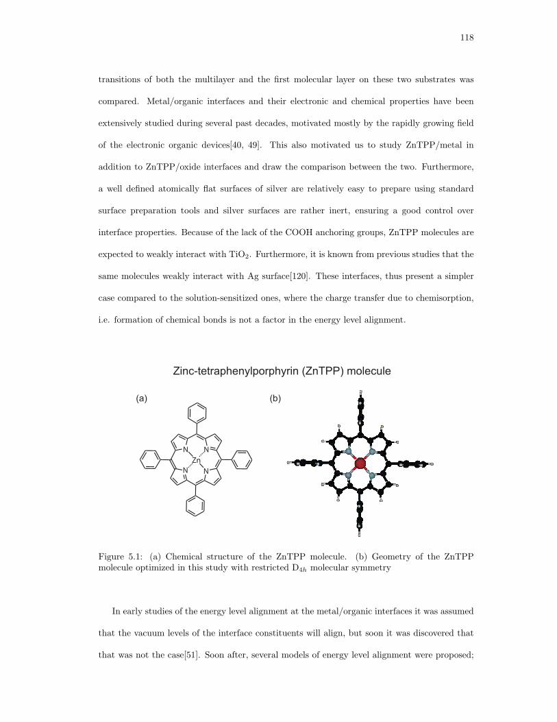
118
transitions of both the multilayer and the first molecular layer on these two substrates was
compared. Metal/organic interfaces and their electronic and chemical properties have been
extensively studied during several past decades, motivated mostly by the rapidly growing field
of the electronic organic devices[40, 49]. This also motivated us to study ZnTPP/metal in
addition to ZnTPP/oxide interfaces and draw the comparison between the two. Furthermore,
a well defined atomically flat surfaces of silver are relatively easy to prepare using standard
surface preparation tools and silver surfaces are rather inert, ensuring a good control over
interface properties. Because of the lack of the COOH anchoring groups, ZnTPP molecules are
expected to weakly interact with TiO2. Furthermore, it is known from previous studies that the
same molecules weakly interact with Ag surface[120]. These interfaces, thus present a simpler
case compared to the solution-sensitized ones, where the charge transfer due to chemisorption,
i.e. formation of chemical bonds is not a factor in the energy level alignment.
Zn
NN
N N
Zinc-tetraphenylporphyrin (ZnTPP) molecule
(a) (b)
Figure 5.1: (a) Chemical structure of the ZnTPP molecule. (b) Geometry of the ZnTPPmolecule optimized in this study with restricted D4h molecular symmetry
In early studies of the energy level alignment at the metal/organic interfaces it was assumed
that the vacuum levels of the interface constituents will align, but soon it was discovered that
that was not the case[51]. Soon after, several models of energy level alignment were proposed;

119
induced density of gap states[121, 122], “push-back” or pillow effect[123], integer charge transfer
model[40, 124], etc. However, a comprehensive and predictive model has not been established
so far. In the majority of studies of the energy level alignment and the electronic structure at
the metal/organic interfaces, metallic thin films prepared under vacuum conditions were used
as the substrate for the organic molecules[125–127]. There is, thus a need for studies on well
defined atomically flat metallic surfaces, prepared and cleaned in ultra-high vacuum conditions.
Such studies could be especially valuable as a benchmark for theoretical calculations.
On the other hand, there has not been very many studies done on the oxide/organic inter-
faces. In case of the metal/organic interfaces the charge exchange between the metal and the
molecules that governs the energy level alignment is happening at the Fermi level of the metal.
Since, in principle, ideal bulk oxides do not have free charges at the Fermi level, the charge
transfer will have to happen to or from some other states in the oxide. Several recent studies
have shown that the charge transfer is indeed happening through either valence or conduction
band of the oxide[128–130]. Other studies focused on the universality of the Fermi level pin-
ning model and were successfully used to describe the energy level alignment of wide variety
of organic/oxide interfaces. From this, a universal equation that can predict the alignment of
the HOMO of the molecule with respect to the Fermi energy of the oxide was deduced[58].
However, the unoccupied states were not measured in this study, and direct prediction of the
alignment of the LUMO with respect to the Fermi level of the first layer of molecules has not
been discussed.
Furthermore, during the photoemission and inverse photoemission measurements, the tech-
niques that are most commonly used to obtain the energy position of HOMO and LUMO, the
molecules in the organic layer are either positively or negatively charged.[56] The energy level
alignment of the HOMO and LUMO with respect to the substrate Fermi level is then expected
to be different at metal/organic and metal oxide/organic interfaces, since these two substrates
would screen the created charges differently. When discussing the energy level alignment, it is
thus important to take charge screening effects of the substrate into account.
120
In this chapter we will present a comprehensive UHV-based study of the both occupied
and unoccupied states using UPS and IPS and energy level alignment of ZnTPP molecules
thermally deposited in-situ on well ordered and atomically flat TiO2(110) and Ag(100) single
crystal surfaces. The adsorption geometry of the molecules in the first layer at these surfaces
has been studied as well using UHV-based scanning tunneling microscopy. To help interpret
the measured electronic structure, quantum chemistry calculations were done on the gas phase
molecule and compared to the experimental spectra. Measured electronic structure of the
multilayer and a monolayer of ZnTPP molecules deposited on these two different interfaces
is compared and discussed and the full energy level alignment diagram for the first layer of
molecules will be presented.
5.2 Experimental methods and sample preparation
Ultraviolet, X-ray and inverse photoemission spectroscopies (UPS, XPS and IPS) as well as
reflection electron energy loss spectroscopy (REELS) were performed in a single ultra-high
vacuum (UHV) experimental chamber. More details about the spectroscopic measurements
and instrumentation can be found in Chapter 2. The UHV chamber was also equipped with
sputtering and annealing tools to prepare clean and well-ordered surfaces in-situ. To probe the
valence band of the samples He II (40.8 eV) photons were used, while He I (21.2 eV) photons were
used to evaluate the work functions and the ionization potentials of the samples. From these
measurements the dipole at the interface between the molecular layer and the substrate was
extracted. Energies in the UPS and IPS spectra were referenced with respect to the Fermi level
of a gold sample in contact with either metal of the oxide substrate. The overall instrumental
resolution for UPS and IPS is estimated to be 0.3 and 0.6 eV, respectively.
Scanning tunneling microscopy (STM) measurements were performed in a separate UHV
chamber also equipped with sputtering and annealing tools for surface preparation. Imaging
was done using an Omicron variable temperature STM (VT-STM) at 300 K.

121
5.2.1 Sample preparation
The rutile TiO2 sample was a commercially produced single-crystal at MTI corporation and
cut to within 0.5 of the (110) plane. Both Ag(100) and TiO2(110) samples were degassed
and prepared in ultrahigh vacuum (UHV) using several cycles of 1 keV Ar+ ion sputtering and
annealing in UHV at 850 K and 900 K, respectively. To prevent extensive surface damage of
TiO2 sample a maximum sputtering current on the sample of 2 µA has been maintained. The
cleanliness of the surfaces was checked using XPS, and the surface termination was assessed by
low energy electron diffraction.
For both STM and spectroscopic measurements (that were done in separate UHV chambers)
the zinc tetraphenylporphyrin (ZnTPP) molecules were evaporated in-situ in UHV at ∼600 K
onto clean and well-ordered silver or TiO2 surfaces using a home built Knudsen cell. During
the deposition the substrates were kept at room temperature. The ZnTPP powder was placed
in a crucible made from alumina (Al2O3) that was located in the Knudsen cell and heated up
using resistively heated Ta filament that was wrapped around it. Evaporation of the molecules
and the thickness of the evaporated ZnTPP film was monitored using a quartz crystal monitor
(QCM) mounted on the same UHV chamber. To ensure the formation of an ordered ZnTPP
film on either surface, the evaporation rate of the molecules was kept at a minimum detectable
by a QCM. To reduce the thickness of an as-evaporated ZnTPP film, samples were subsequently
annealed at a desired temperature and cooled down in UHV before further measurement. An-
nealing was done by using resistively heated tantalum filament that was mounted onto the
bottom of the sample plate. Thermal contact with the heating filament was enabled by fixing
the samples to the sample plate using tantalum straps at the corners of the crystals.
5.3 Computational
Electronic structure calculations, the details of which can be found in Section 2.9, were per-
formed using GAMESS(US)[74] software package on the molecules in gas phase, i.e. not bonded
to the surface. Geometries in local minima on the potential energy surface were calculated in
122
a fixed symmetry group (D4h) using a 6-31G* basis set[80]. The density of states (DOS) was
produced by performing a sum of the individual electronic states convoluted with a 0.7 eV full
width at half maximum Gaussian function. The Gaussian width used here is smaller than the
one used in the studies on the monolayer of tetraphenylporphyrin molecules chemisorbed on the
oxide surfaces presented in Chapters 3 and 4, where the width of 1.2 eV was used. The reason
for smaller width used here is that the features in the UPS and IPS ZnTPP multilayer spectra,
that were used to “simulate” the broadening of the features in the calculated DOS, appear
to be much sharper and more intense than the ones found in one monolayer of chemisorbed
molecules. The reason for sharper and more intense molecular features in the UPS and IPS
spectra of ZnTPP multilayer is increased number of molecules probed (multilayer vs. monolayer
of molecules in previous studies) and it is also indication of high order in UHV deposited films.
5.4 Results and discussion
5.4.1 Monolayer preparation and molecular thermal stability
There are two possible ways to prepare a well defined monolayer of ZnTPP molecules at the
surfaces of Ag(100) and TiO2(110). One way is to deposit a full monolayer of the molecules
directly onto a substrate. This method requires a fine precision of molecular flux during the de-
position and a good calibration of the deposition process. Another way is to deposit a multilayer
thin film of ZnTPP molecules and subsequently anneal the sample to desorb additional layers
from the surface. This thermal desorption method was used previously to prepare a monolayer
of tetraphenylporphyrins[131, 132] with a success and we thus employed the same method in
this study to prepare samples with monolayer coverage of ZnTPP molecules on both Ag(100)
and TiO2(110) surface. Before performing any measurements it is important to determine the
multilayer desorption and molecular decomposition temperature to ensure that the molecules
in the monolayer are thermally stable during sample annealing. For that, both ZnTPP/Ag
and ZnTPP/TiO2 samples were annealed at different temperatures and subsequently studied

123
by XPS.
Figures 5.2(a) and (b) display a series of C 1s core level XPS spectra taken from as deposited
and subsequently annealed ZnTPP/Ag and ZnTPP/TiO2 sample, respectively. The annealing
temperatures are indicated in the figure.
(a)
(c)
Inte
nsity (
arb
. u
nits)
-295 -290 -285 -280
Binding energy (eV)
as deposited
465 K
540 K
620 K
675 K
XPS C 1s
Inte
nsity (
arb
. u
nits)
-295 -290 -285 -280
Binding energy (eV)
(b)ZnTPP/Ag(100)
XPS C 1s
ZnTPP/TiO2(110)
as deposited
560 K
580 K
620 K
670 K
8
6
4
2
0
Co
ve
rag
e (
ML
)
600500400300
Temperature (K)
Figure 5.2: (a) C 1s XPS spectra of ZnTPP/Ag(100) taken at different annealing temperatures.The peak shifts with temperature indicating multilayer desorption. At 675 K C 1s feature splitsin two features, indicating the thermal decomposition of ZnTPP molecule. (b) ZnTPP/Ag(100)film thickness at different annealing temperatures. The thickness is estimated from the Ag 3dfeature in XPS survey spectrum of ZnTPP/Ag(100).
The C 1s core level in XPS shows as one peak found at 284.6 eV. As the samples are
annealed at 540 K, especially evident for the ZnTPP/Ag sample, C 1s peak shifts by 0.3 eV
to lower binding energies, i.e. to the right on the graph, indicating the multilayer desorption
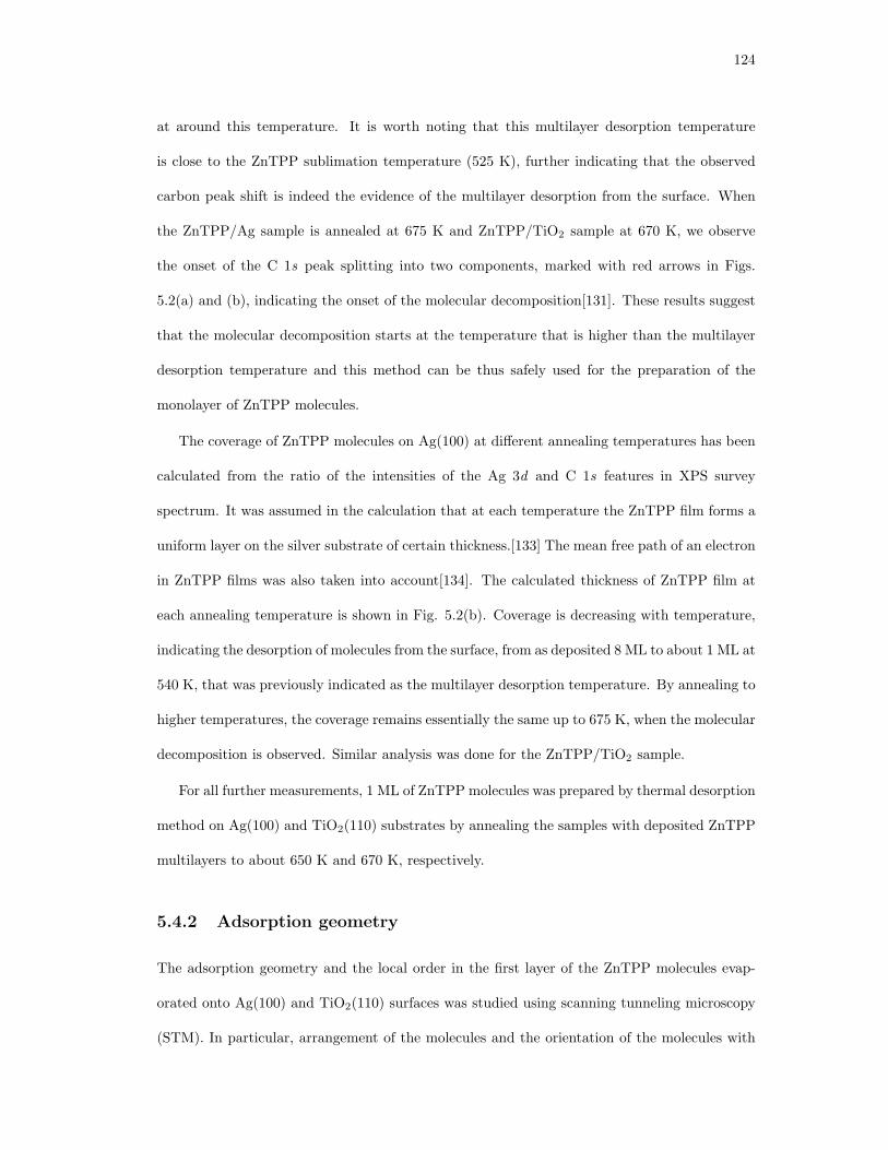
124
at around this temperature. It is worth noting that this multilayer desorption temperature
is close to the ZnTPP sublimation temperature (525 K), further indicating that the observed
carbon peak shift is indeed the evidence of the multilayer desorption from the surface. When
the ZnTPP/Ag sample is annealed at 675 K and ZnTPP/TiO2 sample at 670 K, we observe
the onset of the C 1s peak splitting into two components, marked with red arrows in Figs.
5.2(a) and (b), indicating the onset of the molecular decomposition[131]. These results suggest
that the molecular decomposition starts at the temperature that is higher than the multilayer
desorption temperature and this method can be thus safely used for the preparation of the
monolayer of ZnTPP molecules.
The coverage of ZnTPP molecules on Ag(100) at different annealing temperatures has been
calculated from the ratio of the intensities of the Ag 3d and C 1s features in XPS survey
spectrum. It was assumed in the calculation that at each temperature the ZnTPP film forms a
uniform layer on the silver substrate of certain thickness.[133] The mean free path of an electron
in ZnTPP films was also taken into account[134]. The calculated thickness of ZnTPP film at
each annealing temperature is shown in Fig. 5.2(b). Coverage is decreasing with temperature,
indicating the desorption of molecules from the surface, from as deposited 8 ML to about 1 ML at
540 K, that was previously indicated as the multilayer desorption temperature. By annealing to
higher temperatures, the coverage remains essentially the same up to 675 K, when the molecular
decomposition is observed. Similar analysis was done for the ZnTPP/TiO2 sample.
For all further measurements, 1 ML of ZnTPP molecules was prepared by thermal desorption
method on Ag(100) and TiO2(110) substrates by annealing the samples with deposited ZnTPP
multilayers to about 650 K and 670 K, respectively.
5.4.2 Adsorption geometry
The adsorption geometry and the local order in the first layer of the ZnTPP molecules evap-
orated onto Ag(100) and TiO2(110) surfaces was studied using scanning tunneling microscopy
(STM). In particular, arrangement of the molecules and the orientation of the molecules with
125
respect to the surface was studied. The samples were prepared as described in Section 5.2.1
and 5.4.1. The scanning tunneling microscopy images of the ZnTPP monolayer on Ag(100) and
TiO2(110) surfaces are presented in Figs. 5.3 and 5.4, respectively.
1.4 nm
1.5 nm
(a) (b)
Ag(100)
(c) HOMO-1 HOMO
Figure 5.3: STM images of a monolayer of ZnTPP molecules evaporated onto Ag(100). Allimages are taken at V=-0.8 V and I=0.3 nA. (a) A large area scan of the ordered ZnTPP layer.(b) A close-up image of the ordered ZnTPP molecule monolayer on top of one of the terraceson silver surface. The unit cell dimensions are indicated in the figure. (c) Proposed model ofadsorption of the ZnTPP molecules on Ag(100).
Figure 5.3(a) displays a large-area scan of the ZnTPP monolayer on Ag(100). Molecules
completely cover the terraces and arrange in a long-range highly ordered rectangular lattice.
Step edges shown in the figure correspond to the step edges on the clean silver surface. It is
interesting to note that while the step edges of the clean silver surface have irregular shape,
their appearance is changed after molecular adsorption. As shown in the figure, the step edges
after molecular adsorption feature large stretches of straight parts that seemingly run along the
rows of the adsorbed molecules. This appearance of the step edges can be be explained by the
molecule-induced structural changes at the surface where the highly mobile silver surface atoms
arrange underneath the layer and follow the outlines of the adsorbed molecules. Such behavior
was observed for the adsorption of large organic molecules on Cu[135, 136], as well as the large

126
organic molecules and atoms on Ag surfaces[137, 138].
A close-up image of the ZnTPP molecules adsorbed on one of the terraces at the silver
surface is shown in Fig. 5.3(b). The individual molecules are clearly visible in the figure as
features with donut shaped central part and four additional ovals making a cross. The donut
shaped center represents the porphyrin part of the molecule, with the dip in the image at the
zinc atom located in the center of the donut. Four additional ovals arranged in a cross are the
phenyl rings of the ZnTPP molecule. Since the tunneling voltages used to image surface are
negative, in which case the sample is at negative and the tip at the positive voltage, what is
imaged are the occupied orbitals of the ZnTPP molecules. The observed molecular shape is in
our case mostly representative of the HOMO and HOMO-1 orbitals, shown in Fig. 5.3(c), that
have no weight on the central zinc atom, observed as a dip in the center of the donut, and a little
or no weight on the phenyl rings. The first layer of the ZnTPP molecules thus adsorbs with
their porphyrin rings parallel to the silver surface, while phenyl rings are essentially upright,
as schematically shown in Fig. 5.3(c). Molecules are arranged in a rectangular lattice with the
dimensions indicated in Fig. 5.3(b). Molecules are offset from one another, so that the phenyl
rings on the neighboring molecules form an interlocking structure. This arrangement is most
probably accomplished to minimize the repulsion of the electron clouds located on the phenyl
rings on the neighboring molecules. Similar adsorption geometry of tetraphenylporphyrins on
silver surfaces have been reported in the earlier studies[139].
Similar structure and the adsorption geometry of ZnTPPmonolayer was observed on TiO2(110)
surface as well, as shown in Fig. 5.4.
Over extended distances the molecules order in a rectangular lattice, as shown in Fig. 5.4(a),
similar to the one observed on silver surface. However, in contrast to ZnTPP on Ag(100), the
arrangement and the orientation of the rows of molecules with respect to the surface is not unique
and the molecules appear to adjust to fill up the terraces on the TiO2 surface as efficiently as
possible. In contrast to the step edges on the silver surface, the step edges on the TiO2 surface
retain irregular shape even after adsorption of the molecular layer. Molecule-induced surface
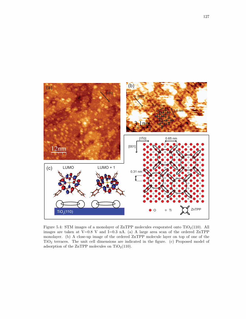
127
[001]
[110]
TiO ZnTPPTiO
2(110)
(c)
(a)
0.65 nm
0.31 nm
[001]
LUMO LUMO + 1
[001]
(b)
1.5 nm
1.4 nm
Figure 5.4: STM images of a monolayer of ZnTPP molecules evaporated onto TiO2(110). Allimages are taken at V=0.8 V and I=0.3 nA. (a) A large area scan of the ordered ZnTPPmonolayer. (b) A close-up image of the ordered ZnTPP molecule layer on top of one of theTiO2 terraces. The unit cell dimensions are indicated in the figure. (c) Proposed model ofadsorption of the ZnTPP molecules on TiO2(110).

128
restructuring is thus negligible in case of TiO2 surface. The ZnTPP/TiO2 surface, in general
looks much rougher than ZnTPP/Ag(100) surface, with substantial part of the surface covered
in adsorbates that can be seen as large white blobs in Fig. 5.4(a). It is possible that these
adsorbates are the second layer of the molecules nucleating on top of the first layer. The first
layer of molecules grows, thus in much ordered way on silver surface compared to TiO2 surface.
The details of the molecular lattice can be seen on the close-up STM image presented in Fig.
5.4(b). Interestingly, the lattice parameters indicated in the figure, are similar to those for the
molecules adsorbed on the silver surface. The neighboring molecules seem to be offset by one
5-fold coordinated Ti row, that runs in the [001] direction indicated in the figure, most likely to
reduce the repulsive interaction between the neighboring phenyl rings. Observed shapes of the
molecules are similar as on the silver surface, with the donut shaped center part, representing
the porphyrin part of the molecule and four ovals extending off from it arranged in a cross,
representing four phenyl rings attached to the main porphyrin ring. Since the applied tunneling
voltage is positive, meaning the sample is at positive and the tip is at negative bias, the orbitals
imaged here are in the unoccupied states of ZnTPP molecules. In our case the the observed
shape is mostly representative of the LUMO and LUMO+1 orbitals, shown schematically in
Fig. 5.4(c). These orbitals don’t have weight on the central zinc atom, that is seen as a dip in
the center of the donut and have little or no weight on the phenyl rings of the molecule.
From this we can conclude that the first layer of ZnTPP molecules adsorbs in a similar
geometry on the TiO2 surface as on the silver surface, i.e., the porphyrin ring lies parallel to the
surface, while the phenyl rings are upright. The model of the molecular adsorption on TiO2(110)
surface and one possible arrangement of the molecules in the lattice is shown schematically in
Fig. 5.4(c).
It is worth noting that in comparison to the adsorption geometry of them-ZnTCPPmolecules
chemisorbed of TiO2(110), studied using STM in Chapter 3, the adsorption geometry of the
ZnTPP molecules on the same surface is found similar. In both cases the porphyrin ring of the
molecule is found parallel to the surface and the phenyl rings are found upright. The orientation
129
of the molecules in the plane of the TiO2(110) surface is also found to be the same. The phenyl
rings of the molecules are found to be rotated by 45 with respect to the 5-fold coordinated Ti
row of the substrate.
To ensure that the imaged ZnTPP layer at both Ag(100) and TiO2(110) is the first molec-
ular layer at the surface, we subsequently heated the samples up to the multilayer desorption
temperature (∼550 K) and imaged the surface after the sample cooled down. For both sur-
faces the structure of the surface and the ZnTPP adsorption geometry remained the same after
such temperature treatment. It is hard, however, from the collected STM images, to discern
the possibility of phenyls rotating to be more parallel with the surface after heating, which was
observed previously after heating the 1 ML of H2TPP/Ag(111) sample to the multilayer desorp-
tion temperature[132]. In the mentioned study the rotation was also confirmed with NEXAFS
measurements. Interestingly, the phenyl rings were upright in the layers of H2TPP molecules
grown on top of a monolayer with such geometry.
5.4.3 Theoretical DOS of ZnTPP in gas phase
The optimized geometry of the ZnTPP molecule, shown in Fig. 5.1(b), was calculated in fixed
molecular D4h symmetry and it is found to be in agreement with previous theoretical and
experimental work on the same or similar molecules[21, 81, 82]. The central porphyrin ring is
found to be planar, while four phenyl rings, attached to it through C-C bond, perpendicular to
it. The large angle between the phenyl and porphyrin rings is mainly due to steric interaction
between the hydrogen atoms located on these two parts of the molecule. Due to such molecular
geometry, there is little or no overlap between π systems on phenyl and porphyrin rings and these
two parts of the molecule are thus essentially electronically decoupled. This has been shown
previously in work of our own group as well as in work of others on similar tetraphenylporphyrin
molecules[21, 75, 81, 82].
The calculated energies of the molecular electronic states for the ZnTPP molecule in gas
phase are shown in Figure 5.5. Each line in the figure represents one molecular electronic states.

130
Inte
nsity(a
rb. u
nits)
-15 -10 -5 0
Energy (eV)
HOMOs LUMOs
Ph
Multi
Multi
Ph / ZnP
Ph
HOMOs
LUMOs
Ph / ZnP
Figure 5.5: Electronic DOS of the ZnTPP molecule. Each line below the DOS represents oneelectronic molecular state. Representative molecular orbitals of indicated DOS features areshown below and above the graph.

131
The molecular DOS, obtained as described in Section 5.2, is shown in Figure 5.5 as a solid curve.
It is important to note that apparent absence of any states above 0 eV in the DOS of the ZnTPP
molecules in Fig. 5.5, is due to a limitation in number of orbitals considered in the calculation,
and not to a real absence of the molecular states above this energy.
In the occupied states of the ZnTPP molecule, extending from ∼ −5 eV to larger negative
binding energies, i.e. to the left on the graph in Fig. 5.5, HOMO and HOMO-1 are found
nearly degenerate and well separated from the rest of the states. HOMO-1 state, with a2u
symmetry is found at −5.02 eV while HOMO, with a1u symmetry is found at −4.95 eV. Both
HOMO and HOMO-1 orbitals are delocalized on the porphyrin macrocycle, with little or no
weight on the phenyl rings. At higher binding energies a sharp feature is found at ∼ −7 eV
comprised mostly of orbitals localized on the phenyl rings with little or no weight on the central
porphyrin ring. However, among the states that contribute to the peak at −7 eV, there are set
of states, found at the lower binding energy foot of the peak at ∼ −6 eV, that are localized on
the porphyrin macrocycle and contain the contribution of the porphyrin π orbitals, as well as Zn
d orbitals. The presence of these states at this energy will be important for a later discussion.
At even higher binding energies, a broad multi-peak features located between −9 to −13 eV
and −13 and −15 eV are composed of states either localized on the porphyrin macrocycle
or on the phenyl rings or delocalized on the whole molecule. In the unoccupied states, that
extend from ∼ −2 eV to smaller negative energies, i.e. to the right on the graph, the LUMO
and the LUMO+1 levels are found degenerate at −2 eV and well separated from the rest of
the unoccupied electronic states. Both LUMOs have eg symmetry and are delocalized on the
porphyrin macrocycle. Above these, states localized mostly on the phenyl rings are found at
∼ −0.2 eV. The representative orbitals from each feature in the calculated DOS described above
are shown in Fig. 5.5.

132
5.4.4 Electronic structure and energy level alignment
The occupied and unoccupied electronic states of the ZnTPP molecules adsorbed on Ag(100)
and TiO2(110) surfaces were probed using UPS and IPS, respectively. The combined UPS
(binding energy < 0 eV) and IPS spectra (binding energy > 0 eV) of clean surfaces and surfaces
with as deposited ZnTPP film that were subsequently annealed are shown for Ag(100) and
TiO2(110) in Figs. 5.6(a) and 5.6(b), respectively. The zero of energy on the graphs refer to
the Fermi energy of the system.
(a) (b)
Inte
nsity (
arb
. u
nits)
-15 -10 -5 0 5
Binding energy (eV)
Clean Ag(100)
as deposited
heated to 540 K
heated to 650 K(1 ML ZnTPP)
Inte
nsity (
arb
. u
nits)
-15 -10 -5 0 5
Binding energy (eV)
Clean TiO2(110)
as deposited
heated to 560 K
heated to 670 K(1 ML ZnTPP)
ZnTPP/Ag(100) ZnTPP/TiO2(110)
Figure 5.6: UPS and IPS spectra of (a) clean Ag(100) and ZnTPP/Ag(100) samples and (b)clean TiO2 and ZnTPP/TiO2 samples after annealing at indicated temperatures.
For the clean Ag(100) surface (upper-most spectrum shown in Fig. 5.6(a)), the occupied
states in UPS consist of rather flat and featureless band extending from the Fermi level (0 eV)
to −3 eV composed mainly of the mixture of 5s and 5p states of silver and an intense two
peaked feature located at binding energies between −3 and −8 eV composed of 4d silver states.

133
The unoccupied states of clean Ag(100) in IPS are dominated by an intense feature peaking
near the Fermi energy attributed to the mixture of empty 5s and 5 p states of silver. This
feature appears intense in the silver IPS spectrum because it is assigned to a direct transition
detected with our angle resolved IPS. The image potential state of Ag(100) is observed at 4.8
eV[140], confirming that the single crystal surface is well ordered after preparation in UHV.
The occupied and unoccupied states of TiO2(110) sample in UPS and IPS are characterized by
the sample features described in Section 3.3.1 of Chapter 3. The valence and the conduction
band edges, as well as the energy band gap of TiO2 were determined by following the procedure
outlined in the same section.
For both surfaces, after deposition of the ZnTPP molecules, UPS and IPS spectra change
drastically and reveal a new set of states attributed to ZnTPP molecules. The occupied and
unoccupied electronic states of multilayer ZnTPP in UPS and IPS on both surfaces are shown
as second curve from the top in Figs. 5.7(a) and (b). After annealing, molecular states become
weaker and states related to the substrate are detected in the UPS and IPS spectra. To be
able to obtain only the molecular contribution to the measured ZnTPP/Ag and ZnTPP/TiO2
spectra at different annealing temperatures, the contribution from the substrates needs to be
subtracted from the spectra. To do that, the clean Ag and TiO2 UPS and IPS spectra are
first scaled and then subtracted from the measured ZnTPP/Ag and ZnTPP/TiO2 spectra. The
scaling factors for the clean Ag UPS and IPS spectra were, as expected, dependent on the
annealing temperature and were determined in such way to remove the Fermi edge at around 0
eV from the spectra containing the organic molecules. Furthermore, the scaling factors for the
clean TiO2 UPS and IPS spectra were chosen as previously explained in Section 3.3.1 of Chapter
3. Since the as-deposited ZnTPP film on both surfaces was thick enough (> 30 A), there was
no detectable substrate contribution in the UPS and IPS spectra of as-deposited ZnTPP/Ag
and ZnTPP/TiO2 samples. It is worth noting that the shape of the UPS and IPS spectra of a
monolayer ZnTPP on TiO2 (last spectrum in Fig. 5.6(b)) is similar to the one of chemisorbed
m-ZnTCPP and p-ZnTCPP on TiO2 presented in Chapters 3 and 4.
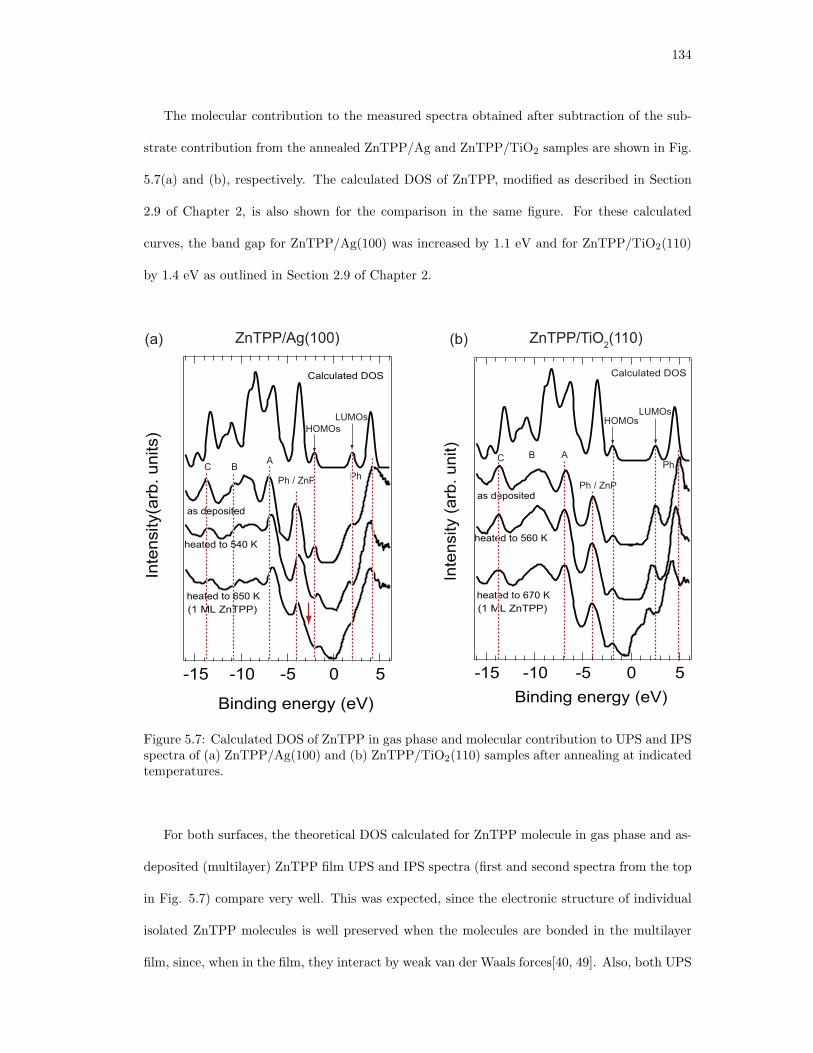
134
The molecular contribution to the measured spectra obtained after subtraction of the sub-
strate contribution from the annealed ZnTPP/Ag and ZnTPP/TiO2 samples are shown in Fig.
5.7(a) and (b), respectively. The calculated DOS of ZnTPP, modified as described in Section
2.9 of Chapter 2, is also shown for the comparison in the same figure. For these calculated
curves, the band gap for ZnTPP/Ag(100) was increased by 1.1 eV and for ZnTPP/TiO2(110)
by 1.4 eV as outlined in Section 2.9 of Chapter 2.
Inte
nsity(a
rb. u
nits)
-15 -10 -5 0 5
Binding energy (eV)
Calculated DOS
(a)
Calculated DOS
(b)
HOMOsLUMOs
ZnTPP/Ag(100) ZnTPP/TiO2(110)
HOMOs
LUMOs
Ph / ZnP PhB
AC
as deposited
heated to 540 K
heated to 650 K
(1 ML ZnTPP)
B AC
Ph / ZnP
Ph
as deposited
heated to 560 K
heated to 670 K
(1 ML ZnTPP)
Inte
nsity (
arb
. u
nit)
-15 -10 -5 0 5
Binding energy (eV)
Figure 5.7: Calculated DOS of ZnTPP in gas phase and molecular contribution to UPS and IPSspectra of (a) ZnTPP/Ag(100) and (b) ZnTPP/TiO2(110) samples after annealing at indicatedtemperatures.
For both surfaces, the theoretical DOS calculated for ZnTPP molecule in gas phase and as-
deposited (multilayer) ZnTPP film UPS and IPS spectra (first and second spectra from the top
in Fig. 5.7) compare very well. This was expected, since the electronic structure of individual
isolated ZnTPP molecules is well preserved when the molecules are bonded in the multilayer
film, since, when in the film, they interact by weak van der Waals forces[40, 49]. Also, both UPS
135
and IPS are surface sensitive techniques, probing only 1 to 2 topmost layers of the ZnTPP thin
film, and thus any possible substrate effects will not be captured in the UPS and IPS spectra
of a ZnTPP multilayer. Furthermore, except for the shifts of the spectral features that will be
addressed later, there are no new features appearing in the UPS and IPS spectra of 1 ML ZnTPP
compared to multilayer ZnTPP spectra on both substrates (second and fourth spectrum in Fig.
5.7) and the general shapes of the spectra are similar. This suggests that there are no new bonds
forming at both interfaces, i.e. there is no chemisorption. The molecule-substrate interaction
for both silver and TiO2 substrate is weak and doesn’t drastically effect the electronic structure
of the adsorbed ZnTPP molecules. Such weak interaction between similar tetraphenylporphyrin
molecules and silver surfaces has been reported earlier[120, 139].
Comparison between the theoretical DOS and the experimental UPS and IPS spectra for
both as-deposited (multilayer) and subsequently annealed ZnTPP films can help identify fea-
tures in the UPS and IPS spectra and assign molecular orbitals that contribute to these features.
In the following analysis we will compare calculated DOS (the upper-most spectrum in Fig. 5.7)
and as-deposited ZnTPP/Ag and ZnTPP/TiO2 UPS and IPS spectra (second spectra in Figs.
5.7(a) and 5.7(b)). Similar analysis can be done on the UPS and IPS spectra taken on the an-
nealed samples. From the comparison of the calculated occupied DOS and the UPS spectra, it
is clear that the feature appearing at about −2 eV in the occupied states of as-deposited spectra
can be assigned to the HOMO-1/HOMO of the molecule. Furthermore, a feature, denoted by
Ph/ZnP in Fig. 5.7, found right below HOMOs at ∼ −4 eV is attributed mostly to the states
localized on the phenyl rings of the molecule. However, several states localized on the porphyrin
ring also contribute to this feature, as discussed previously. Features found at higher binding
energies in the spectra, denoted by A, B and C in Fig. 5.7, are composed of the states localized
either on the porphyrin or the phenyl rings or delocalized over the entire molecule, as shown in
Fig. 5.5. In the unoccupied states, a feature found at ∼ 2 and ∼ 2.5 eV in the IPS spectra of
ZnTPP/Ag and ZnTPP/TiO2, respectively, can be assigned to degenerate LUMO/LUMO+1
states of the molecule. A feature right above LUMOs, denoted with Ph in Fig. 5.7, found at
136
∼ 4.5 eV for ZnTPP/Ag and at ∼ 5 for ZnTPP/TiO2 can be assigned to the states localized
on phenyl rings of the molecule, as shown in Fig. 5.5.
As expected, UPS and IPS spectra of as-deposited ZnTPP film on Ag(100) and TiO2(110)
surfaces (second spectra in Figs. 5.7(a) and (b)) are found to be very similar. The thickness
of the as-deposited film on silver was ∼ 36 A, as determined from the ratio of the Ag 3d and
C 1s features in the XPS spectra, as explained in Section 5.4.1 of this chapter. For TiO2,
determination of the thickness of as-deposited film was not possible, since the substrate Ti
2p core level was not visible in the XPS spectrum due to a thick ZnTPP film present after
deposition. However, it can be estimated, knowing the mean free path λ = 2.7 nm of Ti 2p
photoelectrons (Ek ≈ 950 eV) in ZnTPP film, that the as-deposited ZnTPP film thickness on
TiO2 is larger than ∼ 80 A. In the unoccupied states, LUMOs and phenyl related features
are sharper for ZnTPP/TiO2 and also shifted by ∼ 0.4 eV to higher energies, i.e. to the right
on the graph. Additional preliminary measurements done on ZnTPP/ZnO and ZnTPP/Au
surfaces, that are not presented here, follow a similar trend, with the unoccupied states in of
ZnTPP on ZnO in IPS being sharper than on Au. The origin of this behavior is not clear
yet and further measurements need to be done to understand it. However, one possible reason
for different widths of IPS features can be the difference in the lifetime of an IPS electron
in unoccupied states of ZnTPP on these two substrates. It seems that the lifetime of an
IPS electron is shorter for ZnTPP/silver compared to ZnTPP/TiO2 sample possibly due to
better/faster charge transfer at the ZnTPP/silver interface caused by better order in the film,
as seen from our STM study, presented in Section 5.4.2. On the other hand, the shift in energy
of the features in IPS on Ag compared to TiO2 can be attributed to difference in thickness of
as-deposited films on these two substrates, with thicker ZnTPP film being deposited on TiO2. It
is worth noting that special care has been taken to identify possible charging effects during IPS
measurements on as-deposited films, since charging can cause rigid shift of the IPS spectrum to
the higher binding energies. However, on both ZnTPP/Ag and ZnTPP/TiO2 charging effects
were not observed.

137
Upon annealing and thus decreasing the thickness of as-deposited ZnTPP film, features in
the UPS and IPS spectra of ZnTPP/Ag and ZnTPP/TiO2 shift with respect to the ones in the
multilayer UPS and IPS spectra, as shown in Fig. 5.7. In case of the monolayer ZnTPP/TiO2
sample, after subtraction, there is a shoulder appearing in the IPS spectra close to the Fermi
level. It is possible that after annealing at 670 K some molecules are partially decomposed
at the surface and the states from these molecules contribute to the observed shoulder in the
spectrum.
For the ZnTPP/Ag sample, all features in the UPS spectrum except the feature denoted by
Ph/ZnP in Fig. 5.7(a), shift rigidly towards lower binding energies. For 1 ML of ZnTPP/Ag
shifts of all of these features are of the order of ∼ 0.5 eV. Features that shift, namely, the
HOMOs and features at higher binding energies (A, C and multicomponent feature B) have all
been assigned either to states purely localized on the porphyrin macrocycle (like HOMOs) or
mostly contain either states localized on porphyrin macrocycle or states delocalized over the
whole molecule. The Ph/ZnP feature presents an interesting case since, as mentioned earlier,
states that contribute to this feature are found mostly localized on phenyl rings, but there are
also states at the lower binding energy foot of the feature that or localized on the porphyrin
ring. It is evident, especially from the 1 ML ZnTPP/Ag spectrum in Fig. 5.7(a) that as the
thickness of the film decreases these two types of molecular states shift by different amounts.
The red arrow points to the shoulder appearing on the Ph/ZnP feature in the 1 ML spectrum.
Since features in the spectrum that are attributed to the states localized on the porphyrin ring
only (i.e. HOMOs) shift, it is sensible to assume that the states localized on the porphyrin
ring found at the foot of the Ph/ZnP feature shift by similar amount and contribute to the
shoulder marked by red arrow in the 1 ML ZnTPP spectrum. Furthermore, it seems that the
states localized on the phenyl rings shift much less than the states localized on porphyrin ring
and contribute to the maximum of the Ph/ZnP found at ∼ −4 eV. In the IPS spectrum of
ZnTPP/Ag both LUMOs and phenyl related states shift by approximately the same amount
(∼ 0.3 eV for 1 ML ZnTPP/Ag). It is interesting that, while the shifts of most of the features

138
in the UPS spectra increase with annealing temperature, states in the IPS spectra shift once
the multilayer desorption temperature is reached (540 K) and remain at the same position
with further increase in annealing temperature and decrease in film thickness. The energies of
several prominent features in the UPS and IPS spectra of ZnTPP/Ag at different annealing
temperatures (and different thicknesses) are listed in Table 5.1. The last row in the table
corresponds to 1 ML of ZnTPP on Ag.
Table 5.1: Energy positions of features in UPS and IPS spectra of ZnTPP/Ag(100) with an-nealing temperature in eV
Temp. (K) E(C) E(A) E(Ph/ZnP) E(HOMOs) E(LUMOs) E(Ph)
as-deposited -13.8 -7 -4 -2.1 2 4.2
465 -13.8 -7 -4.1 -2.1 1.7 3.9
520 -13.6 -6.8 -4 -2 1.7 4
620 -13.5 -6.7 -4 -1.8 1.7 4
650 (1 ML) -13.3 -6.7 -3.9 -1.6 1.7 4
Similar energies of HOMOs and LUMOs feature with respect to the Fermi energy have been
measured in UPS and IPS for multilayer (8 ML∼ 36 A) films of H2TPP on Ag(111) at −1.9 eV
and 2.1 eV, respectively[139]. Also, for a ZnTPP thin film (∼ 50 A) on polycrystalline silver
substrate the energy position of HOMOs feature has been measured in UPS to be at ∼ −2.1
eV with respect to the Fermi level, similar to what was found in our study[125].
For the ZnTPP/TiO2 features in the UPS spectrum of the occupied electronic states do not
shift with annealing temperature as thickness of the film decreases and for 1 ML they remain
at the same positions as they were for as-deposited ZnTPP/TiO2. However, both the LUMOs
feature and phenyl related feature, denoted by Ph in Fig. 5.7(b) shift by a similar amount
(∼ 0.7 eV for 1 ML ZnTPP/TiO2) compared to as-deposited ZnTPP/TiO2. The positions of
all peaks at different annealing temperatures (and different thicknesses) in the UPS and IPS
spectra of ZnTPP/TiO2 are listed in Table 5.2. The last row in the table corresponds to 1 ML
of ZnTPP on TiO2.
The change in energies of the frontier orbitals of ZnTPP and the vacuum level with the
annealing temperature (and film thickness) is summarized graphically in Fig. 5.8.
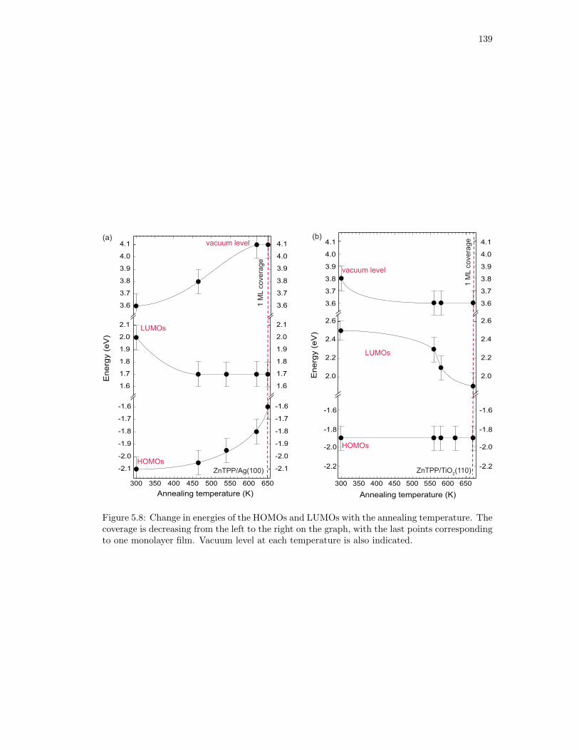
139
En
erg
y (
eV
)
LUMOs
1 M
L c
ove
rag
e
650600550500450400350300
Annealing temperature (K)
HOMOs
2.6
2.4
2.2
2.0
-2.2
-2.0
-1.8
-1.6
-2.1
-2.0
-1.9
-1.8
-1.7
-1.6
En
erg
y (
eV
)
650600550500450400350300
Annealing temperature (K)
2.1
2.0
1.9
1.8
1.7
1.6
LUMOs
HOMOs
1 M
L c
ove
rag
e
ZnTPP/Ag(100) ZnTPP/TiO2(110)
(a) (b)4.1
4.0
3.9
3.8
3.7
3.6
vacuum level
vacuum level
4.1
4.0
3.9
3.8
3.7
3.6
-2.1
-2.0
-1.9
-1.8
-1.7
-1.6
2.1
2.0
1.9
1.8
1.7
1.6
4.1
4.0
3.9
3.8
3.7
3.6
2.6
2.4
2.2
2.0
-2.2
-2.0
-1.8
-1.6
4.1
4.0
3.9
3.8
3.7
3.6
Figure 5.8: Change in energies of the HOMOs and LUMOs with the annealing temperature. Thecoverage is decreasing from the left to the right on the graph, with the last points correspondingto one monolayer film. Vacuum level at each temperature is also indicated.
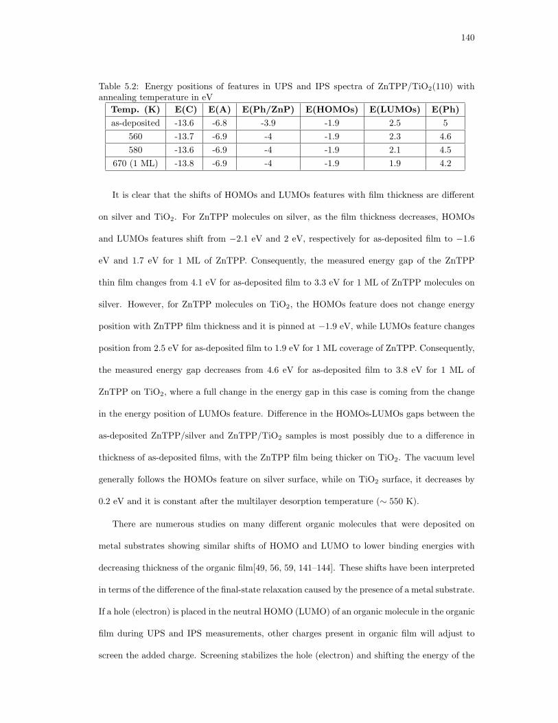
140
Table 5.2: Energy positions of features in UPS and IPS spectra of ZnTPP/TiO2(110) withannealing temperature in eV
Temp. (K) E(C) E(A) E(Ph/ZnP) E(HOMOs) E(LUMOs) E(Ph)
as-deposited -13.6 -6.8 -3.9 -1.9 2.5 5
560 -13.7 -6.9 -4 -1.9 2.3 4.6
580 -13.6 -6.9 -4 -1.9 2.1 4.5
670 (1 ML) -13.8 -6.9 -4 -1.9 1.9 4.2
It is clear that the shifts of HOMOs and LUMOs features with film thickness are different
on silver and TiO2. For ZnTPP molecules on silver, as the film thickness decreases, HOMOs
and LUMOs features shift from −2.1 eV and 2 eV, respectively for as-deposited film to −1.6
eV and 1.7 eV for 1 ML of ZnTPP. Consequently, the measured energy gap of the ZnTPP
thin film changes from 4.1 eV for as-deposited film to 3.3 eV for 1 ML of ZnTPP molecules on
silver. However, for ZnTPP molecules on TiO2, the HOMOs feature does not change energy
position with ZnTPP film thickness and it is pinned at −1.9 eV, while LUMOs feature changes
position from 2.5 eV for as-deposited film to 1.9 eV for 1 ML coverage of ZnTPP. Consequently,
the measured energy gap decreases from 4.6 eV for as-deposited film to 3.8 eV for 1 ML of
ZnTPP on TiO2, where a full change in the energy gap in this case is coming from the change
in the energy position of LUMOs feature. Difference in the HOMOs-LUMOs gaps between the
as-deposited ZnTPP/silver and ZnTPP/TiO2 samples is most possibly due to a difference in
thickness of as-deposited films, with the ZnTPP film being thicker on TiO2. The vacuum level
generally follows the HOMOs feature on silver surface, while on TiO2 surface, it decreases by
0.2 eV and it is constant after the multilayer desorption temperature (∼ 550 K).
There are numerous studies on many different organic molecules that were deposited on
metal substrates showing similar shifts of HOMO and LUMO to lower binding energies with
decreasing thickness of the organic film[49, 56, 59, 141–144]. These shifts have been interpreted
in terms of the difference of the final-state relaxation caused by the presence of a metal substrate.
If a hole (electron) is placed in the neutral HOMO (LUMO) of an organic molecule in the organic
film during UPS and IPS measurements, other charges present in organic film will adjust to
screen the added charge. Screening stabilizes the hole (electron) and shifting the energy of the
141
charged HOMO (LUMO) state towards the middle of the energy gap, effectively decreasing
the energy gap. The screening has several components, the response of the electrons in the
film, the response of the ions in the molecule and the response of the ions in the neighboring
molecules. The largest screening contribution, coming from the rearrangement of the electrons
in the system, is the one that is captured in the UPS and IPS experiment. Ionic contribution
may be also included, however this contribution can be estimated to be much smaller[40, 56].
The HOMO and LUMO states measured in UPS and IPS are thus almost fully relaxed charged
states and their energy separation reflects the transport gap of the organic semiconductor. The
mentioned polarization effects in the organic solids include long-range electrostatic interaction
and they will be affected by the presence of other materials that contain free charges. In
our case, at the interface there is either silver or TiO2, that both have free charges that can
effectively screen the charges created in the ZnTPP film. The presence of free charges in TiO2
is the result of the preparation (sputtering and annealing) of the sample in UHV during which
the oxygen vacancies are created that dope the sample with electrons[145]. This is also evident
from the Fermi level position in TiO2 that is brought close to the conduction band minimum,
whereas for intrinsic undoped TiO2 Fermi level is expected to be in the middle of the gap.
However, we would expect that the density of free charges and their mobility is smaller in
TiO2 compared to silver. It is thus expected that the HOMOs and LUMOs measured in UPS
and IPS are shifted more towards lower binding energies as the distance to the interface with
metal decreases. Effectively, the energy gap of the organic material would decrease with the
decrease in the thickness of the organic layer. This model was successfully applied to several
metal/organic interfaces[56, 142–144]. From this model, however, the HOMOs and LUMOs
should shift by the same amount at each annealing temperature. However, on both surfaces
that is not the case. This is especially evident for the ZnTPP/TiO2 where HOMOs feature
appears to be pinned at −1.9 eV and LUMOs feature is shifting. This suggests that there are
some other electrostatic processes in the film that influence the position of the electronic states
in addition to the image charges in the substrate. It is unclear, however, what these processes

142
are and further measurements need to be done to understand the asymmetrical shifts of features
in UPS and IPS.
It is also observed that the phenyl-related states and ZnP-related states of ZnTPP comprising
the Ph/ZnP feature shift differently with the decrease in thickness of a film on silver substrate,
with phenyl-related feature shifting much less compared to the ZnP one. This behavior can be
explained by different interaction of the states localized on the porphyrin ring with substrate
compared to the states localized on the phenyl rings. As seen from our STM study presented
in Section 5.4.2, ZnP part of the molecule lies parallel to the surface, while phenyl rings are
upright. It is possible that due to different orientation of these two parts of the molecule, the
interaction with the substrate is different and this is causing different shift of the electronic
states upon thickness decrease.
To evaluate the interface dipole, i.e. the offset between the vacuum level of the substrate
and the vacuum level of the ZnTPP film, the secondary electron cutoff was measured in UPS
for the clean surfaces, as-deposited and 1 ML of ZnTPP molecules on silver and TiO2. The
measurement of the secondary electron cutoff and how to extract the vacuum level position
is explained in Section A.2 of Appendix A. Briefly, interface dipole can be directly evaluated
from the shift of the secondary electron cutoff when the ZnTPP molecules are adsorbed on the
clean surface. Figure 5.9(a) displays the secondary electron cutoff in UPS spectrum for clean
Ag(100) shown as black solid line, as-deposited ZnTPP thin film shown as red solid line and
1 ML ZnTPP on Ag shown as red dashed line. After the deposition of ZnTPP film, the edge
shifts by 1 eV to lower energies. However, after preparation of 1 ML of ZnTPP, the edge shifts
back and final shift for 1 ML of ZnTPP on Ag(100) is 0.5 eV to lower energies. Figure 5.9(b)
displays the secondary electron edge in UPS spectrum for clean TiO2(110) shown as black solid
line, as-deposited ZnTPP shown as red solid line and 1 ML of ZnTPP shown as red dashed
line. After deposition of ZnTPP film the secondary electron cutoff shifts by 0.4 eV to lower
energies. However, after preparation of 1 ML of ZnTPP it shifts further and final shift for 1 ML
of ZnTPP on TiO2(110) is 0.6 eV to lower energies. The interface dipole of 1 ML of ZnTPP on
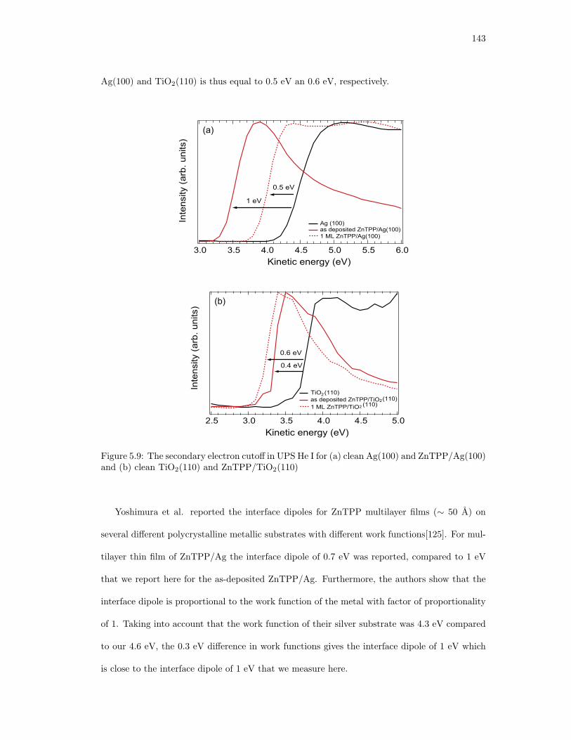
143
Ag(100) and TiO2(110) is thus equal to 0.5 eV an 0.6 eV, respectively.
Inte
nsity (
arb
. u
nits)
6.05.55.04.54.03.53.0
Kinetic energy (eV)
0.5 eV
1 eV
Ag (100) as deposited ZnTPP/Ag(100) 1 ML ZnTPP/Ag(100)
(a)
Inte
nsity (
arb
. u
nits)
5.04.54.03.53.02.5
Kinetic energy (eV)
0.4 eV
0.6 eV
TiO2 (110)
as deposited ZnTPP/TiO2(110)
1 ML ZnTPP/TiO2 (110)
(b)
Figure 5.9: The secondary electron cutoff in UPS He I for (a) clean Ag(100) and ZnTPP/Ag(100)and (b) clean TiO2(110) and ZnTPP/TiO2(110)
Yoshimura et al. reported the interface dipoles for ZnTPP multilayer films (∼ 50 A) on
several different polycrystalline metallic substrates with different work functions[125]. For mul-
tilayer thin film of ZnTPP/Ag the interface dipole of 0.7 eV was reported, compared to 1 eV
that we report here for the as-deposited ZnTPP/Ag. Furthermore, the authors show that the
interface dipole is proportional to the work function of the metal with factor of proportionality
of 1. Taking into account that the work function of their silver substrate was 4.3 eV compared
to our 4.6 eV, the 0.3 eV difference in work functions gives the interface dipole of 1 eV which
is close to the interface dipole of 1 eV that we measure here.
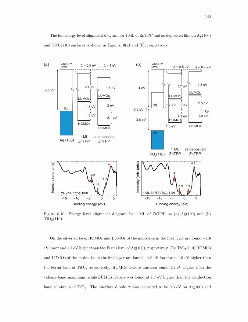
144
The full energy level alignment diagram for 1 ML of ZnTPP and as-deposited film on Ag(100)
and TiO2(110) surfaces is shown in Figs. 5.10(a) and (b), respectively.
-15 -10 -5 0 5
Binding energy (eV)
Inte
nsity (
arb
. u
nits)
1 ML ZnTPP/Ag(100)
Ag (100)1 ML
ZnTPP
EF
HOMOs
LUMOs
vacuumlevel = 0.5 eV
TiO2(110)
EF
vacuumlevel
(a) (b)
CB
VB
4.6 eV2.4 eV
3.6 eV
0.2 eV
4 eV
-1.6
1.7
-15 -10 -5 0 5
Binding energy (eV)
Inte
nsity (
arb
. u
nits)
-1.9 1.9
-4
4.2
-3.9
4
1 ML ZnTPP/TiO2(110)
1.5 eV
1.7 eV
∆ = 0.6 eV∆
1.7 eV
1.6 eV
= 1 eV∆
LUMOs
HOMOs
2 eV
2.1 eV
1.6 eV
as deposited
ZnTPP
1.9 eV
1.9 eV
1.7 eV
LUMOs
HOMOs
= 0.4 eV∆
2.5 eV
1.9 eV
1.3 eV
LUMOs
HOMOs
1 ML
ZnTPP
as deposited
ZnTPP
Figure 5.10: Energy level alignment diagram for 1 ML of ZnTPP on (a) Ag(100) and (b)TiO2(110)
On the silver surface, HOMOs and LUMOs of the molecules in the first layer are found −1.6
eV lower and 1.7 eV higher than the Fermi level of Ag(100), respectively. For TiO2(110) HOMOs
and LUMOs of the molecules in the first layer are found −1.9 eV lower and 1.9 eV higher than
the Fermi level of TiO2, respectively. HOMOs feature was also found 1.5 eV higher than the
valence band maximum, while LUMOs feature was found at 1.7 eV higher than the conduction
band minimum of TiO2. The interface dipole ∆ was measured to be 0.5 eV on Ag(100) and
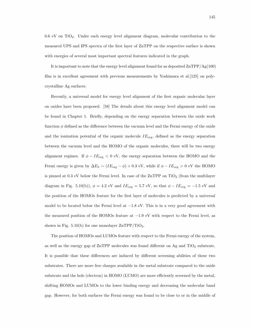
145
0.6 eV on TiO2. Under each energy level alignment diagram, molecular contribution to the
measured UPS and IPS spectra of the first layer of ZnTPP on the respective surface is shown
with energies of several most important spectral features indicated in the graph.
It is important to note that the energy level alignment found for as deposited ZnTPP/Ag(100)
film is in excellent agreement with previous measurements by Yoshimura et al.[125] on poly-
crystalline Ag surfaces.
Recently, a universal model for energy level alignment of the first organic molecular layer
on oxides have been proposed. [58] The details about this energy level alignment model can
be found in Chapter 1. Briefly, depending on the energy separation between the oxide work
function ϕ defined as the difference between the vacuum level and the Fermi energy of the oxide
and the ionization potential of the organic molecule IEorg, defined as the energy separation
between the vacuum level and the HOMO of the organic molecules, there will be two energy
alignment regimes. If ϕ − IEorg < 0 eV, the energy separation between the HOMO and the
Fermi energy is given by ∆Eh ∼ (IEorg − ϕ) + 0.3 eV, while if ϕ − IEorg > 0 eV the HOMO
is pinned at 0.3 eV below the Fermi level. In case of the ZnTPP on TiO2 (from the multilayer
diagram in Fig. 5.10(b)), ϕ = 4.2 eV and IEorg = 5.7 eV, so that ϕ − IEorg = −1.5 eV and
the position of the HOMOs feature for the first layer of molecules is predicted by a universal
model to be located below the Fermi level at −1.8 eV. This is in a very good agreement with
the measured position of the HOMOs feature at −1.9 eV with respect to the Fermi level, as
shown in Fig. 5.10(b) for one monolayer ZnTPP/TiO2.
The position of HOMOs and LUMOs feature with respect to the Fermi energy of the system,
as well as the energy gap of ZnTPP molecules was found different on Ag and TiO2 substrate.
It is possible that these differences are induced by different screening abilities of these two
substrates. There are more free charges available in the metal substrate compared to the oxide
substrate and the hole (electron) in HOMO (LUMO) are more efficiently screened by the metal,
shifting HOMOs and LUMOs to the lower binding energy and decreasing the molecular band
gap. However, for both surfaces the Fermi energy was found to be close to or in the middle of

146
the energy gap of the molecule. This has been observed consistently in our previous studies of
several tetraphenylporphyrin derivatives chemisorbed on oxide surfaces (the studies presented
in Chapters 3 and 4).
5.4.5 Optical gap of ZnTPP and exciton binding energy
In addition to the electronic states of the molecules, the electronic transitions from occupied
to unoccupied states of the molecules in the adsorbed molecular layers were studied in-situ
using reflection electron energy loss spectroscopy (REELS). It has been shown in Section 2.7
of Chapter 2 that the features in the REELS spectrum can be related to the features in the
absorption spectrum of the sample and this has been also confirmed experimentally for the
organic molecules[72]. Furthermore, REELS measurements are surface sensitive, which made
this technique a very well suited for our study of the electronic structure and the electronic
transitions of couple of layers to a monolayer of ZnTPP molecules on silver and TiO2 sub-
strates. Since there is a correspondence between the REELS and the absorption spectra, these
measurements enable us to study the absorption properties, in particular the changes in the
optical gap and exciton binding energy of the molecules with the thickness of the film. All of
the REELS spectra presented in this chapter are taken using 50 eV incident electrons.
Figures 5.11(a) and (b) show REELS spectra for ZnTPP/Ag and ZnTPP/TiO2 samples,
respectively. REELS spectra on both substrates are characterized by a zero-loss peak that is
composed of primary electrons reflected off of the sample without loosing any energy. Energy
loss features appear at energies < 0 eV. The inset in the Figure 5.11(a) shows the loss features of
clean Ag(100), as-deposited ZnTPP/Ag sample and ZnTPP/Ag sample subsequently annealed
at 620 K. The REELS spectrum of clean Ag(100) sample is characterized by a peak found
at −3.9 eV attributed to surface plasmon excitations in the material[146, 147]. When the
ZnTPP molecules are deposited on the substrate, the plasmon peak from silver substrate is not
detected anymore. The REELS spectrum of as-deposited ZnTPP/Ag is characterized by two
loss features, found at −6.8 eV and −2.9 eV. The same loss features are detected in the REELS
147
(a)
-8 -6 -4 -2 0
as deposited ZnTPP annealed ZnTPP at 620 K clean Ag(100)
Inte
nsity (
arb
. u
nits)
-10 -8 -6 -4 -2 0
Energy loss (eV)
ZnTPP/Ag(100)
ZnTPP/TiO2(110)
(b)
Inte
nsity (
arb
. u
nits)
-8 -6 -4 -2 0 2
Energy loss (eV)
-8 -6 -4 -2
as deposited ZnTPP annealed ZnTPP at 580 K
Figure 5.11: REELS spectra of ZnTPP film deposited on (a) Ag(100) and (b) TiO2(110)

148
spectrum of as-deposited ZnTPP/TiO2 at −6.6 eV and −2.9 eV as shown in the inset of Fig.
5.11(b). In the previous work by Otto et al. [148] on a solid benzene sample, a loss feature
detected at −6.9 eV in REELS was attributed to the transition of an electron from HOMO
to LUMO of the benzene. More specifically, this feature was attributed to the 1A1g →1E1u
transition of benzene. From that we can conclude that the higher energy loss feature, found
at −6.8 and −6.6 eV for as-deposited ZnTPP/Ag and ZnTPP/TiO2, respectively, corresponds
to the electron transition from the occupied to the unoccupied molecular orbitals localized on
phenyl rings in the molecule. These orbitals, as we discussed previously, contribute to the
Ph/ZnP (occupied states) and Ph (unoccupied states) features found in the UPS and IPS
spectra of as-deposited films shown in Fig. 5.7. Lower energy loss feature is directly related
to the intense, so-called Soret band located at ∼ 420 nm (∼ 3 eV) in the UV-visible spectrum
of ZnTPP[149]. Another band in the UV-visible spectrum of ZnTPP, Q band, that is much
less intense than Soret band appears at ∼ 600 nm (∼ 2 eV), but since the shoulder of the
zero-loss feature increases at lower energy losses in our experimental setup, it is hard to detect
this feature in REELS spectra. For reference, the UV-visible spectrum of porphyrins and
tetraphenylporphyrins has been described in detail in Appendix C. Furthermore, the energy of
the lower energy loss feature is attributed to the transition from the HOMOs to the LUMOs of
the ZnTPP molecule and thus corresponds to the optical band gap of the molecules in the film.
As the ZnTPP/Ag sample is annealed at 620 K and ZnTPP/TiO2 sample at 580 K, the loss
features shift as shown in the inset of Figs. 5.11(a) and (b). The loss feature attributed to the
transition localized on phenyls shifts by 0.1 eV for ZnTPP/Ag sample and does not shift for
ZnTPP/TiO2 sample, while the loss feature attributed to the transition from the HOMOs to
the LUMOs of the ZnTPP molecule shifts by 0.3 eV to lower energies for both substrates. These
shifts suggest that the optical gap of ZnTPP decreases with the film thickness. The energy of
the transitions localized on phenyls, however, is much less sensitive to the change in thickness.
As expected, for both as-deposited ZnTPP/Ag and ZnTPP/TiO2 films the optical gap mea-
sured in REELS is the same and it equals 2.9 eV. This value is in excellent agreement with

149
the value previously reported in Chapter 4 for the Soret band energy of m- and p-ZnTCPP
molecules measured in UV-visible absorption spectroscopy from the solution in methanol. The
reported wavelength at which the Soret band appears for these molecules is 425 nm which cor-
responds to the energy of 2.9 eV. As the ZnTPP film samples are annealed and the thickness
of the film is decreased, the optical band gap decreases to 2.6 eV for both substrates. This
can be explained by the the simple image potential model, as presented in the recent study by
Garcia-Lastra et al.[150]. As the created exciton carries an electric dipole, upon its creation in
the organic film, the surrounding charges will respond to screen it. Consequently, the energy
needed to create an exciton will decrease, i.e. the optical gap will decrease[150]. Dipole screen-
ing properties are enhanced at interfaces with the highly polarizable materials containing free
charges, as such materials can screen a created dipole more efficiently. As mentioned before in
this chapter, both silver and TiO2 sample in this study contain free charges and as the distance
between the dipole and the surface of these substrates is decreased, it is expected that the
dipole is screened more efficiently, which means that the optical gap of the molecules in the film
decreases as well.
However, the energy of the transition localized on the phenyl rings of the molecule changes
very little (up to 0.1 eV) compared to the optical gap of the molecule. This behavior has
been observed previously when comparing the energies of the same transition (1A1g →1E1u)
of benzene when the molecule is adsorbed on Ag(111) surface and when it is in gas phase. It
has been shown using electron energy loss spectroscopy that the two differ by 0.05 eV[151].
This behavior is consistent with the image potential model, as shown specifically for the case of
benzene on Al(111) in work by Garcia-Lastra et al.[150]. As expected, the image dipole created
by the substrate will depend on the magnitude of the dipole moment created upon the optical
excitation. It has been calculated[150] that the dipole moment created upon 1A1g →1E1u
transition in benzene is negligible. The screening effects of the substrate on this transition will
thus be negligible as well, which is confirmed by the insensitivity of the energy of this transition
with decreasing thickness that we observe in our measurements.
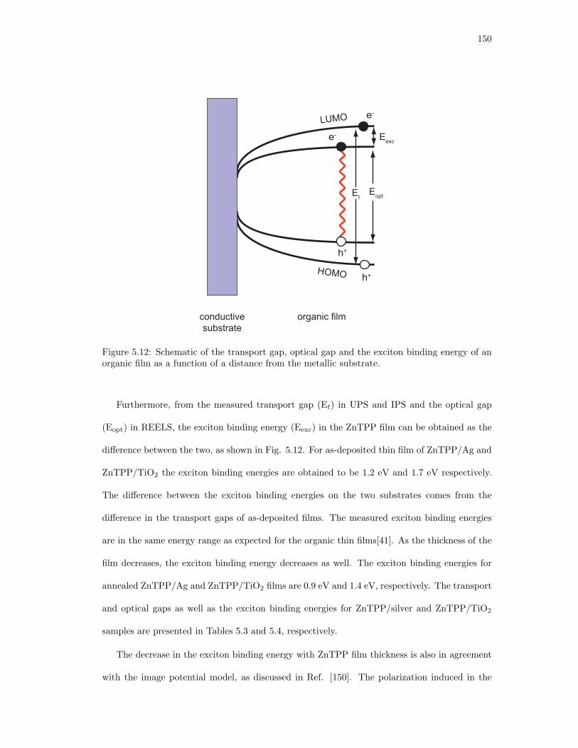
150
Et
Eopt
Eexc
HOMO
LUMO e-
h+
e-
h+
conductive
substrate
organic film
Figure 5.12: Schematic of the transport gap, optical gap and the exciton binding energy of anorganic film as a function of a distance from the metallic substrate.
Furthermore, from the measured transport gap (Et) in UPS and IPS and the optical gap
(Eopt) in REELS, the exciton binding energy (Eexc) in the ZnTPP film can be obtained as the
difference between the two, as shown in Fig. 5.12. For as-deposited thin film of ZnTPP/Ag and
ZnTPP/TiO2 the exciton binding energies are obtained to be 1.2 eV and 1.7 eV respectively.
The difference between the exciton binding energies on the two substrates comes from the
difference in the transport gaps of as-deposited films. The measured exciton binding energies
are in the same energy range as expected for the organic thin films[41]. As the thickness of the
film decreases, the exciton binding energy decreases as well. The exciton binding energies for
annealed ZnTPP/Ag and ZnTPP/TiO2 films are 0.9 eV and 1.4 eV, respectively. The transport
and optical gaps as well as the exciton binding energies for ZnTPP/silver and ZnTPP/TiO2
samples are presented in Tables 5.3 and 5.4, respectively.
The decrease in the exciton binding energy with ZnTPP film thickness is also in agreement
with the image potential model, as discussed in Ref. [150]. The polarization induced in the

151
Table 5.3: Transport and optical gaps and the exciton binding energies in eV forZnTPP/Ag(100)
as-deposited annealed at 620 K
Et 4.1 3.5
Eopt 2.9 2.6
Eexc 1.2 0.9
Table 5.4: Transport and optical gaps and the exciton binding energies in eV forZnTPP/TiO2(110)
as-deposited annealed at 580 K
Et 4.6 4
Eopt 2.9 2.6
Eexc 1.7 1.4
substrate upon exciton creation will also screen the interaction between the electron and the
hole, making the interaction between the charges weaker. As the distance between the substrate
and the exciton is decreasing the interaction is more effectively screened. Consequently, the
exciton binding energy will decrease with the film thickness. This means that the transport gap
and the optical gap are not expected to decrease by the same amount as the distance to the
substrate decreases, as shown in Fig. 5.12, which is what we observe in ZnTPP thin films on
both silver an TiO2.
5.5 Conclusion
In this chapter we present a study of the adsorption geometry, the electronic structure and
the energy level alignment at the interfaces between the UHV-deposited zinc(II)tetraphenyl-
porphyrin (ZnTPP) molecules on Ag(100) and TiO2(110) single crystal samples. The thickness
of the ZnTPP film was decreased by thermal desorption method by annealing the samples at a
particular temperature which enabled us to study the electronic properties of as-deposited film
as well as the first layer of the molecules at the interface.
Scanning tunneling microscopy was used to study the adsorption geometry of the first layer
of molecules on both substrates. We conclude that the first layer of molecules adsorbs with
the main zinc porphyrin ring parallel to the surface while the phenyl rings are oriented upright.

152
Molecules form an ordered layer on both surfaces, however, the order of the layer is much higher
on Ag(100) compared to the TiO2(110) surface.
Electronic states of the ZnTPP molecules in a multilayer and the monolayer were probed
using UPS and IPS. As the thickness of the film decreases from multilayer to a monolayer, we
observe no new states appearing in the UPS and IPS spectra indicating that there are no new
bonds forming at the interface, and that the interaction between the molecules and the substrate
is weak. Furthermore, we observe a decrease in the transport band gap as the thickness of the
film decreases on both substrates that we attribute to more efficient screening of the charged
states in the film by the silver and TiO2 substrates. However, we find that the HOMOs and
LUMOs feature do not shift by the same amount at each annealing temperature. This behavior
is not understood and further measurements are required to explain it.
The energy level alignment of the HOMOs and LUMOs of the first molecular layer with
respect to the Fermi energy of the substrate was found different on silver an TiO2 with both
HOMOs and LUMOs shifted towards lower binding energies for the molecules adsorbed on
silver. This difference is possibly due to different screening abilities of the substrates. However,
the position of HOMOs on both surfaces with respect to the Fermi level of the system was found
in agreement with the data available in literature. In particular, our data correspond very well
with the recently proposed universal model for energy level alignment at the oxide/organic
interfaces.
The electronic excitations that are closely related to the optical absorption properties of
the molecules were studied in REELS. From the REELS spectra we were able to deduce the
optical gap of the ZnTPP molecules in the film. Furthermore, from the known transport gap
from the UPS and IPS measurements and known optical gap from REELS measurements we
obtained the exciton binding energy of the ZnTPP molecules in the film. As the thickness
of the film decreases, we observe that both the optical gap and the exciton binding energy
decrease. This behavior can be explained by screening of the dipole created upon the excitation
by the substrate. As the thickness of the film decreases, the distance between the dipole and

153
the image dipole decreases which both decreases the energy of the dipole, i.e. the optical gap
of the molecule and the interaction between the electron and the hole in the dipole becomes
weaker, i.e. binding energy decreases.
We thus observe the image charge and image dipole effects on the electronic structure, the
energy level alignment and the electronic excitations in the ZnTPP films deposited on both
silver and TiO2.
154
Bibliography
[1] D. M. Chapin, C. S. Fuller, and G. L. Pearson. Journal of Applied Physics, 25:676–677,
1954.
[2] http://www.heliatek.com/wp-content/uploads/2012/04/120427 PI Heliatek-world-
record-10 7-percent-efficiency.pdf.
[3] Aswani Yella, Hsuan-Wei Lee, Hoi Nok Tsao, Chenyi Yi, Aravind Kumar Chandiran,
Md.Khaja Nazeeruddin, Eric Wei-Guang Diau, Chen-Yu Yeh, Shaik M Zakeeruddin, and
Michael Gratzel. Science, 334:629–634, 2011.
[4] B. O’Regan and M. Gratzel. Nature, 353:737, 1991.
[5] Yousuke Ooyama and Yutaka Harima. European Journal of Organic Chemistry,
2009:2903–2934, 2009.
[6] Anders Hagfeldt, Gerrit Boschloo, Licheng Sun, Lars Kloo, and Henrik Pettersson. Chem-
ical Reviews, 110:6595–6663, 2010.
[7] R. B. Woodward, W. A. Ayer, J. M. Beaton, F. Bickelhaupt, R. Bonnett, P. Buchschacher,
G. L. Closs, H. Dutler, J. Hannah, F. P. Hauck, S., A. Langemann, E. Le Goff, W. Leim-
gruber, W. Lwowski, J. Sauer, Z. Valenta, and H. Volz. Journal of the American Chemical
Society, 82:3800–3802, 1960.
[8] W S Caughey, G A Smythe, D H O’Keeffe, J E Maskasky, and M I Smith. Journal of
Biological Chemistry, 250:7602–7622, 1975.
[9] W.M. Campbell, A.K. Burrell, D.L. Officer, and K.W. Jolley. Coord. Chem. Rev.,
248:1363, 2004.

155
[10] M. Gouterman. The Journal of Chemical Physics, 30:1139, 1963.
[11] J.-H. Chou, H. S. Nalwa, M. E. Kosal, N. A. Rakow, and K. S. Suslick. In The Porphyrin
Handbook, volume 6. Academic Press, 2000.
[12] M.K. Nazeeruddin, R. Humphry-Baker, D.L. Officer W.M. Campbell, A.K. Burrell, and
M. Gratzel. Langmuir, 20:6514, 2004.
[13] Robert S. Loewe, Arounaguiry Ambroise, Kannan Muthukumaran, Kisari Padmaja,
Andrey B. Lysenko, Guru Mathur, Qiliang Li, David F. Bocian, Veena Misra, and
Jonathan S. Lindsey. The Journal of Organic Chemistry, 69:1453–1460, 2004.
[14] Lukas Schmidt-Mende, Wayne M. Campbell, Qing Wang, Kenneth W. Jolley, David L.
Officer, Md. K. Nazeeruddin, and Michael Gratzel. Chem. Phys. Chem, 6:1253, 2005.
[15] Wayne M. Campbell, Kenneth W. Jolley, Pawel Wagner, Klaudia Wagner, Penny J.
Walsh, Keith C. Gordon, Lukas Schmidt-Mende, Mohammad K. Nazeeruddin, Qing
Wang, Michael Gratzel”, and David L. Officer. The Journal of Physical Chemistry C,
111:11760–11762, 2007.
[16] Jonathan R. Stromberg, Andras Marton, Hooi Ling Kee, Christine Kirmaier, James R.
Diers, Chinnasamy Muthiah, Masahiko Taniguchi, Jonathan S. Lindsey, David F. Bocian,
Gerald J. Meyer, and Dewey Holten. The Journal of Physical Chemistry C, 111:15464–
15478, 2007.
[17] Chinnasamy Muthiah, Masahiko Taniguchi, Han-Je Kim, Izabela Schmidt, Hooi Ling
Kee, Dewey Holten, David F. Bocian, and Jonathan S. Lindsey. Photochemistry and
Photobiology, 83:1513, 2007.
[18] C.-F. Lo, L. Luo, E. W.-G. Diau, I.-J. Chang, and C.Y. Lin. Chem. Comm., page 1430,
2006.
[19] Ching-Yao Lin, Chen-Fu Lo, Liyang Luo, Hsueh-Pei Lu, Chen-Shiung Hung, and Eric
Wei-Guang Diau. The Journal of Physical Chemistry C, 113:755–764, 2009.
156
[20] Chih-Wei Chang, Liyang Luo, Chung-Kung Chou, Chen-Fu Lo, Ching-Yao Lin, Chen-
Shiung Hung, Yuan-Pern Lee, and Eric Wei-Guang Diau. The Journal of Physical Chem-
istry C, 113:11524–11531, 2009.
[21] P. J. Walsh, K. C. Gordon, D. L. Officer, and W. M. Campbell. J. Mol. Struct.:
THEOCHEM, 759:17, 2006.
[22] J. Rochford and E. Galoppini. Langmuir, 24:5366, 2008.
[23] Y. Tachibana, S.A. Haque, I.P. Mercer, J.R. Durrant, and D.R. King. J. Phys. Chem. B,
104:1198, 2000.
[24] N. Aratani, N. Osuka, H.S. Cho, and D. Kim. J. Photochem. Photobiol. C, 3:25, 2002.
[25] J. Rochford, D. Chu, A. Hagfeldt, and E. Galoppini. J. Am. Chem. Soc., 129:4655, 2007.
[26] J Schnadt, J Schiessling, J.N OShea, S.M Gray, L Patthey, M.K.-J Johansson, M Shi,
J Krempasky, J Ahlund, P.G Karlsson, P Persson, N Martensson, and P.A Br˙Surf. Sci.,
540:39 – 54, 2003.
[27] Michael Odelius, Petter Persson, and Sten Lunell. Surf. Sci., 529:47 – 58, 2003.
[28] Kim S. Finnie, John R. Bartlett, and James L. Woolfrey. Langmuir, 14:2744–2749, 1998.
[29] A. Vittadini, A. Selloni, F. P. Rotzinger, and M. Gratzel. J. Phys. Chem. B, 104:1300–
1306, 2000.
[30] M. K. Nazeeruddin, R. Humphrey-Baker, P. Liska, and M. Gratzel. J. Phys. Chem. B,
107:8981–8987, 2003.
[31] Hsueh-Pei Lu, Chen-Yuan Tsai, Wei-Nan Yen, Chou-Pou Hsieh, Cheng-Wei Lee, Chen-Yu
Yeh, and Eric Wei-Guang Diau. J. Phys. Chem. C, 113:20990–20997, 2009.
[32] C. W. Tang and S. A. VanSlyke. Applied Physics Letters, 51:913–915, 1987.
[33] J. H. Burroughes, D. D. C. Bradley, A. R. Brown, R. N. Marks, K. Mackay, R. H. Friend,
P. L. Burns, and A. B. Holmes. Nature, 347:539, 1990.
157
[34] Francis Garnier, Ryad Hajlaoui, Abderrahim Yassar, and Pratima Srivastava. Science,
265:1684–1686, 1994.
[35] H. Sirringhaus, T. Kawase, R. H. Friend, T. Shimoda, M. Inbasekaran, W. Wu, and E. P.
Woo. Science, 290:2123–2126, 2000.
[36] C. W. Tang. Applied Physics Letters, 48:183–185, 1986.
[37] N. S. Sariciftci, L. Smilowitz, A. J. Heeger, and F. Wudl. Science, 258:1474–1476, 1992.
[38] Kezhao Xing, Mats Fahlman, Michael Logdlund, Doni A. dos Santos, Vincent Parente,
Roberto Lazzaroni, Jean-Luc Bredas, Richard W. Gymer, and William R. Salaneck. Ad-
vanced Materials, 8:971–974, 1996.
[39] Toshio Nishi, Kaname Kanai, Yukio Ouchi, Martin R. Willis, and Kazuhiko Seki. Chemical
Physics Letters, 414:479 – 482, 2005.
[40] Slawomir Braun, William R. Salaneck, and Mats Fahlman. Advanced Materials, 21:1450,
2009.
[41] I.G. Hill, A. Kahn, Z.G. Soos, and R.A. Pascal Jr. Chem. Phys. Lett., 327:181, 2000.
[42] K. Seki. Molecular Crystals and Liquid Crystals Incorporating Nonlinear Optics, 171:255–
270, 1989.
[43] L. E. Lyons. J. Chem. Soc., 1957:5001, 1957.
[44] N. Sato, K. Seki, and H. Inokuchi. J. Chem. Soc. Faraday Trans. 2, 77:1621, 1981.
[45] Ishii et al., Adv. Mater., 11, p.605 (1999). c⃝WILEY-VCH Verlag GmbH, D-69469 Wein-
heim, 1999 0935-9648/99/0806-0608.
[46] R.W. Strayer, W. Mackie, and L.W. Swanson. Surface Science, 34:225 – 248, 1973.
[47] N. D. Lang and W. Kohn. Phys. Rev. B, 1:4555–4568, 1970.
[48] N. D. Lang and W. Kohn. Phys. Rev. B, 3:1215–1223, 1971.

158
[49] Hisao Ishii, Kiyoshi Sugiyama, Eisuke Ito, and Kazuhiko Seki. Advanced Materials,
11:605–625, 1999.
[50] N. D. Lang and W. Kohn. Phys. Rev. B, 8:6010–6012, 1973.
[51] H. Ishii and K. Seki. Electron Devices, IEEE Transactions on, 44:1295 –1301, 1997.
[52] P. Nielsen. Photogr. Sci. Eng., 18:186, 1974.
[53] D. P. Woodruff and T. A. Delchar. Modern tachniques of surface science. Cambridge,
1988.
[54] S. M. Sze and Kwok K. Ng. Physics of semiconducting deveices. Wiley-Interscience, 2007.
[55] Takashi Minakata, Masaru Ozaki, and Hideaki Imai. Journal of Applied Physics, 74:1079–
1082, 1993.
[56] F. Amy, C. Chan, and A. Kahn. Organic Electronics, 6:85, 2005.
[57] Shizuo Tokito, Koji Noda, and Yasunori Taga. J. Phys. D: Appl. Phys., 29:2750, 1996.
[58] Mark T. Greiner, Michael G. Helander, Wing-Man Tang, Zhi-BinWang, Jacky Qiu, and
Zheng-Hong Lu. Nature Materials, 11:76, 2011.
[59] I. G. Hill, A. J. Makinen, and Z. H. Kafafi. Applied Physics Letters, 77:1825, 2000.
[60] T. Koopmans. Physica, 1:104, 1934.
[61] A. Szabo and N. S. Ostlund. Modern Quantum Chemistry. Dover Publications, Inc., 1996.
[62] P. D. Johnson and J. W. Davenport. Physical Review B, 31:7521, 1985.
[63] G. Ertl and J. Koopers. Low energy electrons and surface chemistry. Weinheim, 1985.
[64] N. Stoffel and P. Johnson. Nuclear Instruements and Review of Methods in Physics
Research, 234:230, 1985.
[65] S. Johnson, P. Hulbert, R. Garrett, and M. Howells. Review of Scientific Instruments,
57:1324, 1986.

159
[66] G. Binnig and H. Rohrer. IBM Journal od Research and Development, 30:4, 1986.
[67] G. Binnig and H. Rohrer. Reviews of Modern Physics, 59:615, 1987.
[68] J. A. Kubby and J. J.Boland. Surface Science Reports, 26:63, 1996.
[69] J. Tersoff and D. R. Hamann. Physical Review B, 31:805, 1985.
[70] E. Galoppini. Coordination Chemistry Reviews, 248:1283, 2004.
[71] R. D. Leapman, P. Rez, and D. F. Mayers. Journal of Chemical Physics, 72:1232, 1980.
[72] E. Salomon, N. Papageorgiou, Y. Ferro, and J.M. Layet. Thin Solid Films, 466:259, 2004.
[73] J. Stohr. NEXAFS Spectroscopy. Springer, 2003.
[74] M.W. Schmidt, K.K. Baldridge, J.A. Boatz, S.T. Elbert, M.S. Gordon, J.H. Jensen,
S. Koseki, N. Matsunaga, K.A. Nguyen, S.J. Su, T.L. Windus, M. Dupuis, and J.A.
Montgomery. J. Comput. Chem., 14:1347, 1993. Used GAMESS(US) version January
12th 2009 R3.
[75] S. Rangan, S. Katalinic, R. Thorpe, R.A. Bartynski, J. Rochford, and E. Galoppini. J.
Phys. Chem. C, 114:1139, 2010.
[76] Elena Galoppini and Jonathan Rochford. J. Chem. Phys. B, 110:16159–16161, 2006.
[77] Norma R. de Tacconi, Wilaiwan Chanmanee, Krishnan Rajeshwar, Jonathan Rochford,
and Elena Galoppini. The Journal of Physical Chemistry C, 113:2996–3006, 2009.
[78] Akira Sasahara, Chi Lun Pang, and Hiroshi Onishi. The Journal of Physical Chemistry
B, 110:4751–4755, 2006.
[79] Masatoshi Ikeda, Naoki Masatoshi, Liyuan Han, Akira Sasahara, and Hiroshi Onishi.
Langmuir, 24:8056–8060, 2008.
[80] K.L. Schuchardt, B.T. Didier, T. Elsethagen, L. Sun, V. Gurumoorthi, J. Chase, J. Li,
and T.L. Windus. J. Chem. Inf. Model., 47:1045–1052, 2007.

160
[81] M.-S. Liao and S. Scheiner. J. Chem. Phys., 117:205, 2002.
[82] M.-S. Liao, P. Bonifassi, J. Leszczinsky, and M.-J. Huang. Mol. Phys., 106:147, 2008.
[83] E.I. Solomon and V.E. Henrich. Surf. Sci. Spectra, 5:186, 1998.
[84] Note that this number cannot be directly measured for this molecule but is an estimation
from the comparison with the other ZnTPP derivtaives.
[85] C.C. Cudia, P. Vilmercati, R. Larciprete, C. Capek, G. Zampieri, L. Sangaletti,
S. Pagliara, A. Verdini, A. Cossaro, L. Floreano, A. Morgante, L. Petaccia, S. Lizzit,
C. Battocchio, G. Polzonetti, and A. Goldoni. Surf. Sci., 600:4013, 2006.
[86] Norman Schmidt, Rainer Fink, and Wolfgang Hieringer. Journal of Chemical Physics,
133:054703, 2010.
[87] It can be noticed that in the case of a perfectly flat adsorption of the m-ZnTPP molecules
on the surface, the N 1s NEXAFS peaks should be extinct for θ=0. This absence of
this total extinction might have several causes. First, the surfaces have been sensitized
in solution so as to obtain results close to the solar cells preparations and exposed to
air briefly. It is possible that some of the non dichroic signal arise from atmospheric
contaminants. Second, if at low coverage molecules can find adsorption sites suitable for a
flat geometry, it is most likely that at high coverage some molecules will bind though only
one or two COOH anchoring groups in a non flat geometry. Finally, the surface roughness
as to be considered: a rutile TiO2(110) can be produced with large terraces, however
ZnO(1120) surfaces are characterized by smaller terraces thus inducing more step edges
adsorption sites. This might explain in part why the NEXAFS dichroism is much smaller
on the ZnO(1120) surface. It can be however concluded from the NEXAFS results that
even at high coverage, the m-ZnTCPP are adsorbed in majority flat at the surface of both
wide band gap semiconductors.

161
[88] M. Gervaldo, F. Fungo, E.N. Durantini, J.J. Silber, L. Sereno, and L. Otero. J. Phys.
Chem. B, 109:20953, 2005.
[89] D. F. Marsh and L. M. Mink. J. Chem. Ed., 73:1181, 1996.
[90] C. Khandelwal and J.L. Roebber. Chem. Phys. Lett., 34:355, 1975.
[91] T. Hashimoto, Y.-K. Choe, H. Nakano, and K. Hirao. J. Phys. Chem. A, 103:1894, 1999.
[92] K. Seki, E. Ito, and H. Ishii. Synth. Met., 91:137, 1997.
[93] D.P. Piet, D. Danovich, H. Zuilhof, and E.J.R. Sudholter. J. Chem. Soc., Perkin Trans.
2, page 1653, 1999.
[94] K. Takahashi, T. Iwanaga, T. Yamaguchi, T. Komura, and K. Murata. Synth. Met.,
123:91, 2001.
[95] K. Miyairi, E. Itoh, and Y. Hashimoto. Thin Solid Films, 438:147, 2003.
[96] Yu-Xiang Weng, Long Li, Yin Liu, Li Wang, and Guo-Zhen Yang. The Journal of Physical
Chemistry B, 107:4356–4363, 2003.
[97] P.C. Hariharan and J.A. Pople. Theoret. Chimica Acta, 28:213, 1973.
[98] V.A. Rassolov, J.A. Pople, M.A. Ratner, and T.L. Windus. J. Chem. Phys., 109:1223,
1998.
[99] M. Gouterman. J. Chem. Phys., 33:1523, 1960.
[100] K.A. Nguyen and R. Pachter. J. Chem. Phys., 114:10757, 2001.
[101] G.D. Dorough, J.R. Miller, and F.M. Huennekens. J. Am. Chem. Soc., 73:4315, 1951.
[102] J.B. Allison and R.S. Becker. J. Phys. Chem., 67:2675, 1963.
[103] K. Kalyanasundaram and M. Neumann-Spallart. J. Phys. Chem., 86:5163, 1982.
[104] E. Rabinowitch. Rev. Mod. Phys., 16:226, 1944.
162
[105] D.W.Thomas and A.E. Martell. J. Am. Chem. Soc., 78:1338, 1956.
[106] H-Z. Yu, J.S. Baskin, and Ahmed H. Zewail. J. Phys. Chem. A, 106:9837, 2002.
[107] H-Z. Yu, J.S. Baskin, and Ahmed H. Zewail. J. Phys. Chem. A, 106:9845, 2002.
[108] R.F. Khairutidinov and N. Serpone. J. Phys. Chem. B, 103:761, 1999.
[109] D.J. Quimby and F.R. Longo. J. Am. Chem. Soc., 97:5111, 1975.
[110] G.H. Barnett, M.F. Hudson, and K.M. Smith. J. Chem. Soc. Perkin Trans. I, page 1401,
1975.
[111] J.J. Yeh and I. Lindau. Atomic Data and Nuclear Data Tables, 32:1, 1985.
[112] A. Ghosh. Acc. Chem. Res., 31:189, 1998.
[113] Y. Zhu, S. Zhou, Y. Kan, and Z. Su. Int. J. Quant. Chem, 107:1614, 2007.
[114] H. Ryeng, E. Gonzalez, and A. Ghosh. J. Phys. Chem. B, 112:15158, 2008.
[115] E.B. Fleischer. J. Am. Chem. Soc., 85:1353, 1963.
[116] E.S.Schmidt and T.S. Calderwood. Inorg. Chem., 25:3718, 1986.
[117] J. Seth, V. Palaniappan, T.E. Johnson, S. Prathapan, J.S. Lindsey, and D.F. Bocian. J.
Am. Chem. Soc., 116:10578, 1994.
[118] C. Bruckner, P.C.D. Foss, J.O. Sullivan, R. Pelto, M. Zeller, R.R. Birge, and G.Crundwell.
Phys. Chem. Chem. Phys., 8:2402, 2006.
[119] A. Ghosh. J. Mol. Struct.: THEOCHEM, 388:359, 1996.
[120] Carla Castellarin-Cudia, Patrizia Borghetti, Giovanni Di Santo, Mattia Fanetti, Rosanna
Larciprete, Cinzia Cepek, Paolo Vilmercati, Luigi Sangaletti, Alberto Verdini, Albano
Cossaro, Luca Floreano, Alberto Morgante, and Andrea Goldoni. ChemPhysChem,
11:2248–2255, 2010.
163
[121] H. Vazquez, W. Gao, F. Flores, and A. Kahn. Energy level alignment at organic hetero-
junctions: Role of the charge neutrality level. Phys. Rev. B, 71:041306, 2005.
[122] H. Vazquez, F. Flores, and A. Kahn. Organic Electronics, 8:241 – 248, 2007.
[123] H. Vazquez, Y. J. Dappe, J. Ortega, and F. Flores. The Journal of Chemical Physics,
126:144703, 2007.
[124] Carl Tengstedt, Wojciech Osikowicz, William R. Salaneck, Ian D. Parker, Che-H. Hsu,
and Mats Fahlman. Applied Physics Letters, 88:053502, 2006.
[125] D. Yoshimura, Hisao Ishii, S. Narioka, M. Sei, T. Miyazaki, Y. Ouchi, S. Hasegawa,
Y. Harima, Kazuo Yamashita, and K. Seki. Journal of Electron Spectroscopy and Related
Phenomena, 78:359, 1996.
[126] S. Narioka, H. Ishii, Y. Ouchi, T. Yokoyama, T. Ohta, and K. Seki. The Journal of
Physical Chemistry, 99:1332–1337, 1995.
[127] I. G. Hill, A. Rajagopal, A. Kahn, and Y. Hu. Appl. Phys. Lett., 73:662, 1998.
[128] M. Kroger, S. Hamwi, J. Meyer, T. Riedl, W. Kowalsky, and A. Kahn. Applied Physics
Letters, 95:123301, 2009.
[129] Michele Sessolo and Henk J. Bolink. Advanced Materials, 23:1829–1845, 2011.
[130] Hyunbok Lee, Sang Wan Cho, Kyul Han, Pyung Eun Jeon, Chung-NamWhang, Kwangho
Jeong, Kwanghee Cho, and Yeonjin Yi. Applied Physics Letters, 93:043308, 2008.
[131] Thomas Lukasczyk, Ken Flechtner, Lindsay R. Merte, Norbert Jux, Florian Maier,
J. Michael Gottfried, and Hans-Peter Steinruck. J. Phys. Chem. C, 111:3090, 2007.
[132] G. Di Santo, S. Blankenburg, C. Castellarin-Cudia, M. Fanetti, P. Borghetti, L. San-
galetti, L. Floreano, A. Verdini, E. Magnano, F. Bondino, C. A. Pignedoli, M.-T. Nguyen,
R. Gaspari, D. Passerone, and A. Goldoni. Chem. Eur. J. 14359., 17:14354.
164
[133] Ariana L. Bramblett, Maximiliane S. Boeckl, Kip D. Hauch, Buddy D. Ratner, Tomikazu
Sasaki, and J. W. Rogers Jr. Surf. Interface Anal., 33:506, 2002.
[134] Seah M. P. and Dench W. A. Surf. Interface Anal., 1:2, 1979.
[135] F. Rosei, M. Schunack, P. Jiang, A. Gourdon, E. Lægsgaard, I. Stensgaard, C. Joachim,
and F. Besenbacher. Science, 296:328–331, 2002.
[136] Miao Yu, Wei Xu, Youness Benjalal, Regis Barattin, Erik Lægsgaard, Ivan Stensgaard,
Mohamed Hliwa, Xavier Bouju, Andr Gourdon, Christian Joachim, Trolle Linderoth, and
Flemming Besenbacher. Nano Research, 2:254–259, 2009.
[137] Matthias Bohringer, Richard Berndt, and Wolf-Dieter Schneider. Phys. Rev. B, 55:1384–
1387, 1997.
[138] S.-L. Chang, J.-M. Wen, P. A. Thiel, S. Gunther, J. A. Meyer, and R. J. Behm. Phys.
Rev. B, 53:13747–13752, 1996.
[139] Geoffrey Rojas, Xumin Chen, Cameron Bravo, Ji-Hyun Kim, Jae-Sung Kim, Jie Xiao,
Peter A. Dowben, Yi Gao, Xiao Cheng Zeng, Wonyoung Choe, and Axel Enders. J. Chem.
Phys. C, 114:9408, 2010.
[140] F. J. Himpsel and J. E. Ortega. Phys. Rev. B, 46:9719, 1992.
[141] R. Schlaf, P. G. Schroeder, M. W. Nelson, B. A. Parkinson, P. A. Lee, K. W. Nebesny, ,
and N. R. Armstrong. Journal of Applied Physcis, 86:1499, 1999.
[142] I. G. Hill, A. J. Makinen, and Z. H. Kafafi. Journal of Applied Physics, 88:889, 2000.
[143] M. G. Helander, M. T. Greiner, Z. B. Wang, and Z. H. Lu. Phys. Rev. B, 81:153308, 2010.
[144] E.V. Tsiper, Z.G. Soos, W. G ao b, and A. Kahn. Chem. Phys. Lett., 360:47, 2002.
[145] U. Diebold. Surf. Sci. Rep., 48:53, 2003.
[146] Gar B. Hoflund, Zoltan F. Hazos, and Ghaleb N. Salaita. Phys. Rev. B, 62:11126–11133,
2000.

165
[147] M.P. Seah. Surface Science, 24:357 – 369, 1971.
[148] A. Otto and M. J. Lynch. Aust. J. Phys., 23:609, 1970.
[149] Mario Nappa and Joan S. Valentine. Journal of the American Chemical Society, 100:5075–
5080, 1978.
[150] J. M. Garcia-Lastra and K. S. Thygesen. Phys. Rev. Lett., 106:187402, 2011.
[151] Ph. Avouris and J. E. Demuth. The Journal of Chemical Physics, 75:4783–4794, 1981.
[152] Douglas A. Skoog, F. James Holler, and Timothy A. Nieman. Principles of instrumental
analysis. Saunders College Publishing, 1998.
[153] M. Kasha, H. R. Rawls, and Ashraf M. El-Bayoumi. Pure Appl. Chem., 11:371, 1965.
[154] M. Gouterman. Journal of Molecular Spectroscopy, 6:138, 1961.
[155] M. Gouterman and G. H. Wagniere. Journal of Molecular Spectroscopy, 11:108, 1963.
[156] W. T. Simpson. Journal of Chemical Physics, 17:1218, 1949.
[157] H. C. Longuet-Higgins, C. W. Rector, and J. R. Platt. Journal of Chemical Physics,
18:1174, 1950.
[158] J.C. Slater. Phys. Rev., 34:1293, 1929.
[159] E. Kaxiras. Atomic and Electronic Structure of Solids. Cambridge University Press, 2003.
[160] P. Hohenberg and W. Kohn. Phys. Rev., 136:B864, 1964.
[161] W. Kohn and L.J. Sham. Phys. Rev., 140:A1133, 1965.
[162] L. Hedin and B.I. Lundqvist. J. Phys. C, 4:2064, 1971.
[163] J.P. Perdew and A. Zunger. Phys. Rev. B, 23:5048, 1981.
[164] J.P. Perdew and Y. Wang. Phys. Rev. B, 33:8800, 1986.
[165] A.D. Becke. J. Chem. Phys., 98:1372, 1993.

166
[166] J.P. Perdew, M. Ernzerhof, and K. Burke. J. Chem. Phys., 105:9982, 1996.
[167] A.D. Becke. Phys. Rev. A, 38:3098, 1988.
[168] A.D. Becke. J. Chem. Phys., 98:5648, 1993.
[169] C. Lee, W. Yang, and R.G. Parr. Phys. Rev. B, 37:785, 1988.
[170] J.C. Slater. Phys. Rev., 36:57, 1930.
[171] W.J. Hehre, R. Ditchfield, and Pople J.A. J. Chem. Phys., 56:2257, 1972.
[172] J.D. Dill and J.A. Pople. J. Chem. Phys., 62:2921, 1975.
[173] M.M. Francl, W.J. Petro, W.J. Hehre, J.S. Binkley, M.S. Gordon, D.J. DeFrees, and J.A.
Pople. J. Chem. Phys., 77:3654, 1982.
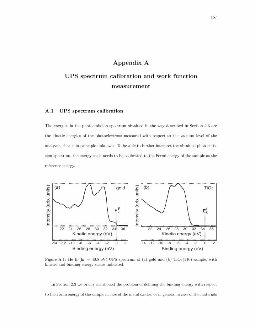
167
Appendix A
UPS spectrum calibration and work function
measurement
A.1 UPS spectrum calibration
The energies in the photoemission spectrum obtained in the way described in Section 2.3 are
the kinetic energies of the photoelectrons measured with respect to the vacuum level of the
analyzer, that is in principle unknown. To be able to further interpret the obtained photoemis-
sion spectrum, the energy scale needs to be calibrated to the Fermi energy of the sample as the
reference energy.
-14 -12 -10 -8 -6 -4 -2 0 2
Binding energy (eV)
Inte
nsity (
arb
. units)
3634323028262422
Kinetic energy (eV)
gold(a)
Inte
nsity (
arb
. units)
3634323028262422
Kinetic energy (eV)
-14 -12 -10 -8 -6 -4 -2 0 2
Binding energy (eV)
(b) TiO2
EkF
EkF
Figure A.1: He II (hν = 40.8 eV) UPS spectrum of (a) gold and (b) TiO2(110) sample, withkinetic and binding energy scales indicated.
In Section 2.3 we briefly mentioned the problem of defining the binding energy with respect
to the Fermi energy of the sample in case of the metal oxides, or in general in case of the materials
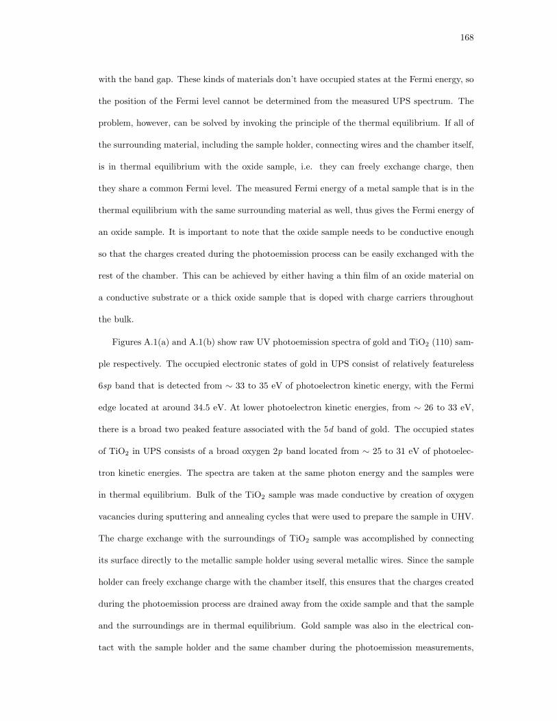
168
with the band gap. These kinds of materials don’t have occupied states at the Fermi energy, so
the position of the Fermi level cannot be determined from the measured UPS spectrum. The
problem, however, can be solved by invoking the principle of the thermal equilibrium. If all of
the surrounding material, including the sample holder, connecting wires and the chamber itself,
is in thermal equilibrium with the oxide sample, i.e. they can freely exchange charge, then
they share a common Fermi level. The measured Fermi energy of a metal sample that is in the
thermal equilibrium with the same surrounding material as well, thus gives the Fermi energy of
an oxide sample. It is important to note that the oxide sample needs to be conductive enough
so that the charges created during the photoemission process can be easily exchanged with the
rest of the chamber. This can be achieved by either having a thin film of an oxide material on
a conductive substrate or a thick oxide sample that is doped with charge carriers throughout
the bulk.
Figures A.1(a) and A.1(b) show raw UV photoemission spectra of gold and TiO2 (110) sam-
ple respectively. The occupied electronic states of gold in UPS consist of relatively featureless
6sp band that is detected from ∼ 33 to 35 eV of photoelectron kinetic energy, with the Fermi
edge located at around 34.5 eV. At lower photoelectron kinetic energies, from ∼ 26 to 33 eV,
there is a broad two peaked feature associated with the 5d band of gold. The occupied states
of TiO2 in UPS consists of a broad oxygen 2p band located from ∼ 25 to 31 eV of photoelec-
tron kinetic energies. The spectra are taken at the same photon energy and the samples were
in thermal equilibrium. Bulk of the TiO2 sample was made conductive by creation of oxygen
vacancies during sputtering and annealing cycles that were used to prepare the sample in UHV.
The charge exchange with the surroundings of TiO2 sample was accomplished by connecting
its surface directly to the metallic sample holder using several metallic wires. Since the sample
holder can freely exchange charge with the chamber itself, this ensures that the charges created
during the photoemission process are drained away from the oxide sample and that the sample
and the surroundings are in thermal equilibrium. Gold sample was also in the electrical con-
tact with the sample holder and the same chamber during the photoemission measurements,

169
and thus in thermal equilibrium with the oxide sample. For gold sample, photoelectrons that
have the highest kinetic energy are the ones originating from the Fermi level of gold. However,
measured gold Fermi edge is broadened, mostly by the influence of the limited electron analyzer
resolution. In order to obtain the kinetic energy of the electrons coming from the Fermi level,
the point of the maximal slope at the high kinetic energy edge in the spectrum is taken and the
kinetic energy of the electrons that originate at the Fermi level (EFk ) is found to be 34.5 eV.
The kinetic energy corresponding to the Fermi level for the TiO2 sample is the same as for the
gold sample because of the two samples were in thermal equilibrium.
The energy scale on the TiO2 spectrum now can be converted to the binding energy scale
with respect to its Fermi energy as zero (EB = 0 eV) using the equation
EB = Ek − EFk , (A.1)
where Ek is the measured kinetic energy of the photoelectrons and EFk is the kinetic energy of
the photoelectrons originating from the Fermi level, so that the binding energy EB is a negative
quantity. New binding energy scales are shown underneath the kinetic energy scales for both
gold and TiO2 samples in figures A.1 (a) and (b) respectively.
A.2 Obtaining the work function and the ionization potential using
UPS
To obtain a full energy alignment diagram at the interfaces between the adsorbed molecules
and metal or metal oxide substrates, work functions and ionization potentials of the interface
constituents need to obtained. Such measurements are especially important for the evaluation
of the interface dipoles created upon molecule adsorption.
Besides studying the occupied valence states, UPS can also be used to obtain the work
function and the ionization potential of the sample. This is accomplished by measuring a so-
called secondary electron background cutoff in the low kinetic energy range of the UPS spectrum.
Apart from the primary photoelectrons that is, the electrons that don’t lose any energy on the
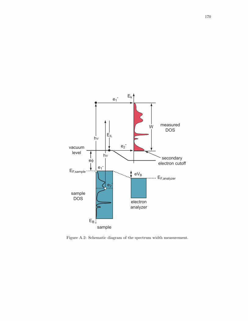
170
sample
DOS
EB
sample
Ek
electron
analyzer
eφ
vacuum
levelhν
EILhν
e1-
e2-
secondary
electron cutoff
EF,sample
EF,analyzer
W
eVB
measured
DOS
e1-
e2-
Figure A.2: Schematic diagram of the spectrum width measurement.

171
way out from the solid, there are also secondary electrons in the UPS spectrum. These electrons
are generated by primary electrons that lost varying amounts of energy on the way out. In most
cases they contribute to the smooth secondary electron background in the UPS spectrum, that
increases drastically with decreasing the electron kinetic energy. Fig. A.2 illustrates how the
work function and the ionization potential measurement is done by describing two electrons
that represent the high and the low kinetic energy edges of the spectrum in the figure. In this
measurement, the sample is negatively biased with respect to the detector by an amount VB,
which shifts all the states up in energy so that the low energy edge of the spectrum can be clearly
detected. Electron e−1 is emitted from the Fermi level of the sample and thus contributes to
the high kinetic energy edge of the spectrum. Electron e−2 is originally bound in a state in the
middle of the valence band. It absorbs a photon and makes transition to an excited state, but
also subsequently loses it’s kinetic energy by inelastic scattering (EIL). Its final state energy is
at the vacuum energy, so it escapes the sample, but with the kinetic energy that is lowest of all
of the collected electrons. The width of the spectrum (W ) is given by the difference between
the high and low kinetic energy edges of the spectrum.
Subtracting the spectrum width (W ) from the incident photon energy (hν) gives the energy
difference between the highest occupied electronic state and the vacuum level. In a metal this
energy is equal to the metal work function, ϕ, that is defined by the equation
Ek = hν + EB − eϕ, (A.2)
where Ek is the kinetic energy of the photoelectron, ~ν is the photon energy and EB is the
binding energy of the electron in the solid. On the other hand, in an insulator, the energy
difference between the photon energy hν and the spectrum width W is known as the ionization
potential, IP, and it equals the sum of the energy band gap (Eg) and the electron affinity (χ),
as given by Eq. (A.3).
hν −W = Eg + eχ. (A.3)
These quantities are denoted for a metal and an insulating sample in Figs. A.3(a) and A.3(b),
respectively.

172
Ek
eφ
vacuum
level
hν
EF
W
Ek
vacuum
level
W
eχ
hν
Eg
IP
(a) (b)
CB
VB
Figure A.3: Schematic energy diagram showing the most important quantities for (a) a metallicand (b) an insulating sample.
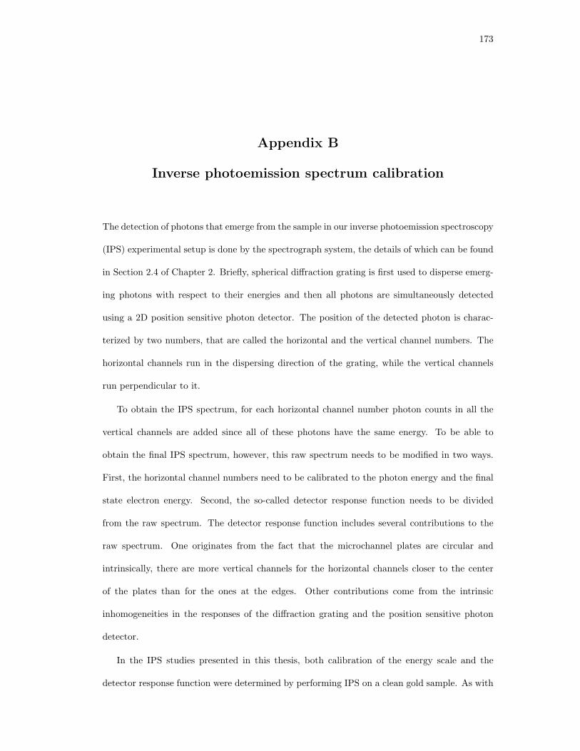
173
Appendix B
Inverse photoemission spectrum calibration
The detection of photons that emerge from the sample in our inverse photoemission spectroscopy
(IPS) experimental setup is done by the spectrograph system, the details of which can be found
in Section 2.4 of Chapter 2. Briefly, spherical diffraction grating is first used to disperse emerg-
ing photons with respect to their energies and then all photons are simultaneously detected
using a 2D position sensitive photon detector. The position of the detected photon is charac-
terized by two numbers, that are called the horizontal and the vertical channel numbers. The
horizontal channels run in the dispersing direction of the grating, while the vertical channels
run perpendicular to it.
To obtain the IPS spectrum, for each horizontal channel number photon counts in all the
vertical channels are added since all of these photons have the same energy. To be able to
obtain the final IPS spectrum, however, this raw spectrum needs to be modified in two ways.
First, the horizontal channel numbers need to be calibrated to the photon energy and the final
state electron energy. Second, the so-called detector response function needs to be divided
from the raw spectrum. The detector response function includes several contributions to the
raw spectrum. One originates from the fact that the microchannel plates are circular and
intrinsically, there are more vertical channels for the horizontal channels closer to the center
of the plates than for the ones at the edges. Other contributions come from the intrinsic
inhomogeneities in the responses of the diffraction grating and the position sensitive photon
detector.
In the IPS studies presented in this thesis, both calibration of the energy scale and the
detector response function were determined by performing IPS on a clean gold sample. As with
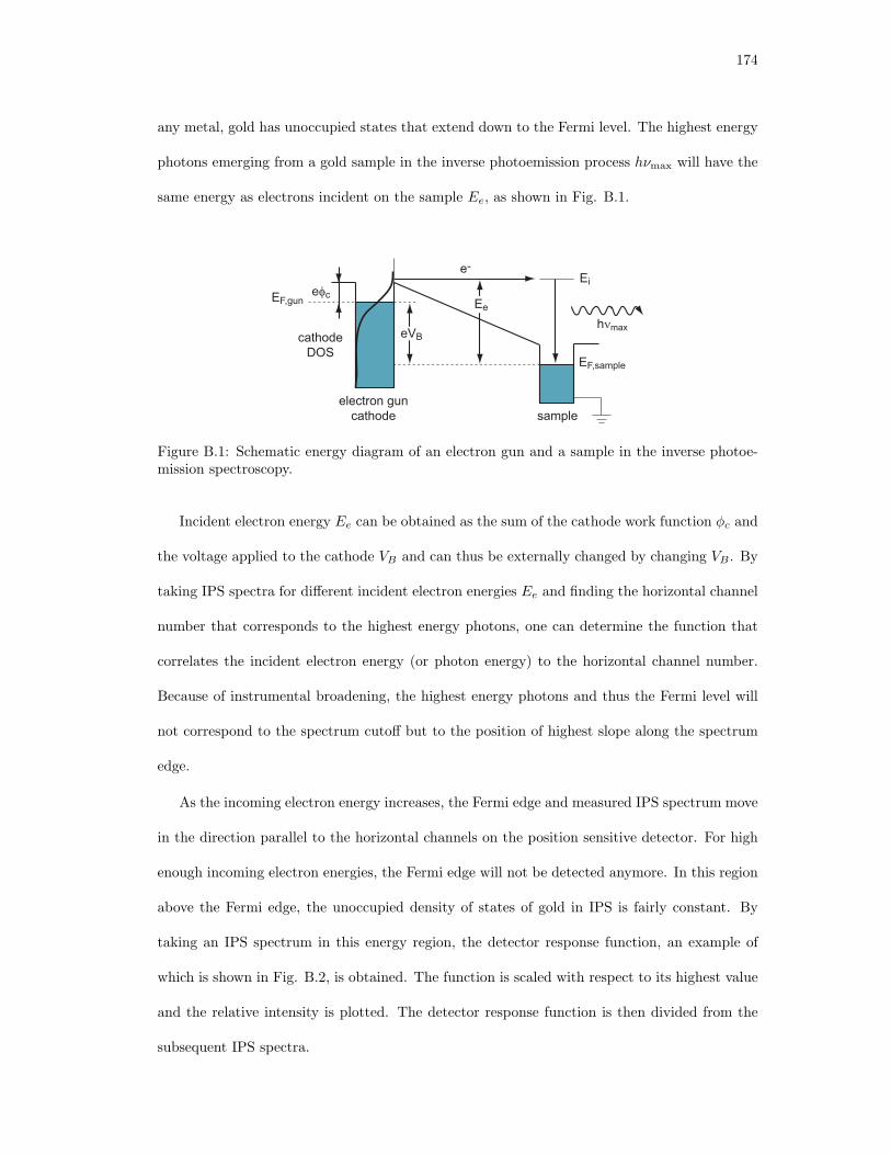
174
any metal, gold has unoccupied states that extend down to the Fermi level. The highest energy
photons emerging from a gold sample in the inverse photoemission process hνmax will have the
same energy as electrons incident on the sample Ee, as shown in Fig. B.1.
eφc
eVB
EF,gun
EF,sample
cathode
DOS
e-Ei
hνmax
electron gun
cathode sample
Ee
Figure B.1: Schematic energy diagram of an electron gun and a sample in the inverse photoe-mission spectroscopy.
Incident electron energy Ee can be obtained as the sum of the cathode work function ϕc and
the voltage applied to the cathode VB and can thus be externally changed by changing VB. By
taking IPS spectra for different incident electron energies Ee and finding the horizontal channel
number that corresponds to the highest energy photons, one can determine the function that
correlates the incident electron energy (or photon energy) to the horizontal channel number.
Because of instrumental broadening, the highest energy photons and thus the Fermi level will
not correspond to the spectrum cutoff but to the position of highest slope along the spectrum
edge.
As the incoming electron energy increases, the Fermi edge and measured IPS spectrum move
in the direction parallel to the horizontal channels on the position sensitive detector. For high
enough incoming electron energies, the Fermi edge will not be detected anymore. In this region
above the Fermi edge, the unoccupied density of states of gold in IPS is fairly constant. By
taking an IPS spectrum in this energy region, the detector response function, an example of
which is shown in Fig. B.2, is obtained. The function is scaled with respect to its highest value
and the relative intensity is plotted. The detector response function is then divided from the
subsequent IPS spectra.

175
1.0
0.9
0.8
0.7
0.6
0.5
0.4
Re
lative
in
ten
sity
250200150100500
Channel number
Figure B.2: An example of the detector response function.
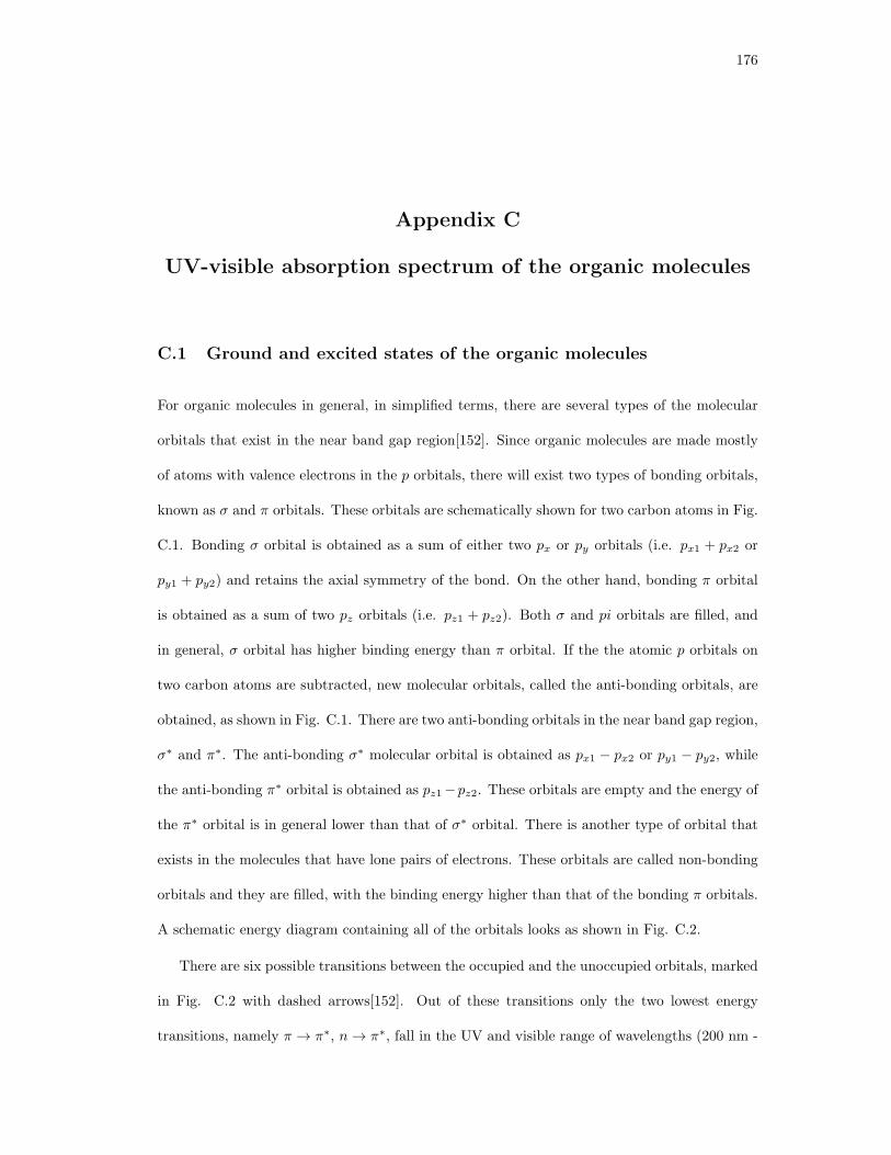
176
Appendix C
UV-visible absorption spectrum of the organic molecules
C.1 Ground and excited states of the organic molecules
For organic molecules in general, in simplified terms, there are several types of the molecular
orbitals that exist in the near band gap region[152]. Since organic molecules are made mostly
of atoms with valence electrons in the p orbitals, there will exist two types of bonding orbitals,
known as σ and π orbitals. These orbitals are schematically shown for two carbon atoms in Fig.
C.1. Bonding σ orbital is obtained as a sum of either two px or py orbitals (i.e. px1 + px2 or
py1 + py2) and retains the axial symmetry of the bond. On the other hand, bonding π orbital
is obtained as a sum of two pz orbitals (i.e. pz1 + pz2). Both σ and pi orbitals are filled, and
in general, σ orbital has higher binding energy than π orbital. If the the atomic p orbitals on
two carbon atoms are subtracted, new molecular orbitals, called the anti-bonding orbitals, are
obtained, as shown in Fig. C.1. There are two anti-bonding orbitals in the near band gap region,
σ∗ and π∗. The anti-bonding σ∗ molecular orbital is obtained as px1 − px2 or py1 − py2, while
the anti-bonding π∗ orbital is obtained as pz1−pz2. These orbitals are empty and the energy of
the π∗ orbital is in general lower than that of σ∗ orbital. There is another type of orbital that
exists in the molecules that have lone pairs of electrons. These orbitals are called non-bonding
orbitals and they are filled, with the binding energy higher than that of the bonding π orbitals.
A schematic energy diagram containing all of the orbitals looks as shown in Fig. C.2.
There are six possible transitions between the occupied and the unoccupied orbitals, marked
in Fig. C.2 with dashed arrows[152]. Out of these transitions only the two lowest energy
transitions, namely π → π∗, n → π∗, fall in the UV and visible range of wavelengths (200 nm -
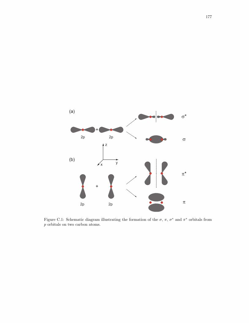
177
2p 2p
σ*
σ
π*
π2p 2p
+
+
(a)
(b)x
y
z
Figure C.1: Schematic diagram illustrating the formation of the σ, π, σ∗ and π∗ orbitals fromp orbitals on two carbon atoms.

178
800 nm) and these transitions are, thus, the most important ones for the UV-visible absorption
spectroscopy.
en
erg
yσ∗
σ
π∗
π
n
These are
normally empty
These contain bonding
pairs of electrons
These contain lone
pairs of electrons
(anti-bonding)
(anti-bonding)
(non-bonding)
(bonding)
(bonding)
Figure C.2: Schematic molecular energy diagram with the transitions between occupied andunoccupied states denoted with dashed arrows.
For each transition there are two different excited states, called the singlet and the triplet.
In the singlet excited state, the total electron spin of the system is S=0 while in the triplet
state total electron spin equals S=1. The names of the excited states originate from their
multiplicities, that are given as 2S+1. For the singlet state, the multiplicity is 1, while for
the triplet state it is 3. In Fig. C.3 singlet and triplet states are schematically depicted. If
Singlet ground
stateSinglet excited
state
Triplet excited
state
Figure C.3: Schematic energy diagram of the singlet and triplet excited states with spins ofelectrons denoted with arrows.
the ground state of the system has no net electron spin, the excitation of one valence electron
without its spin flipping results in the singlet excited state. If the electron spin is, however,
flipped in the process, the excited state will be triplet. Triplet states are always lower in energy
than singlet states. This originates from the electron-electron exchange and correlation effects
and it is usually formulated as a rule similar to the atomic Hund’s rule. Simply put, because

179
of the exchange interaction, two electrons with the spins pointing in the opposite directions
tend to spend more time close to each other than if the electrons that have spins pointing in
the same direction. Thus, the Coulomb interaction is weaker for two electrons that have spins
pointing in the same direction. This lowers the total energy of the excited state configuration
of the triplet with respect to the singlet excited sate.
C.2 Aggregation and molecular exciton coupling model
Porphyrin molecules, since they have a large π orbital system extending on the macrocycle,
tend to interact via long range van der Waals-like attractive forces and aggregate[22, 25, 70].
Aggregation effects are more pronounced if the molecules are bonded to some substrate and
they especially affect the UV-visible absorption spectrum. Upon aggregation, features in the
molecular UV-visible spectrum shift. These shifts are explained by a simple molecular exciton
coupling model that takes into account coupling of excitons, i.e. coupling of the transition
dipole moments on the neighboring molecules in an aggregate.
There are two types of aggregates that the organic molecules in general tend to aggregate to,
called the H and J-aggregates[153]. In H-aggregates, the molecules are stacked “face-to-face”,
whereas in J-aggregates they are stacked “head-to-tail”. These two types of composites will
have different absorption properties and thus different UV-visible absorption spectra compared
to the isolated constituent molecule. For example, J-aggregates show so-called J-bands that
are shifted to longer wavelengths (lower energies) compared to the single molecule UV-visible
absorption bands. H-aggregates will show H-bands that are shifted towards shorter wavelengths
(higher energies) compared to the single molecule absorption bands.
In H-aggregates, in simplest possible arrangement where the molecules are stacked “face-
to-face” and the transition dipoles are parallel to each other, there are two possible exciton
coupling states. The first one is where the transition moments on the neighboring molecules
are in-phase and the second one is when the transition dipole moments are out-of-phase (Fig.
C.4(a)). Electrostatically, the out-of-phase arrangement is energetically preferred and this state

180
(a)
Parallel transition dipoles
Ground
state
Excited
state
Monomer
levels
Dimer
levels
Dipole
phases
Blue-shift
(b)
In-line transition dipoles
Ground
state
Excited
state
Monomer
levels
Dimer
levels
Dipole
phases
Red-shift
H-aggregate J-aggregate
Figure C.4: Schematic diagram of (a) H- and (b) J-aggregates and corresponding excited states.
will have lower energy than the state where the transition dipole moments are all in-phase. The
excited state of the H-aggregate will, thus split into two excited states due to exciton coupling.
For the out-of-phase excited state, however, the total transition dipole moment vanishes, since
transition dipole moments on the neighboring molecules cancel. The transition to the out-of-
phase excited state is thus forbidden while the transition to the in-phase state is allowed. This
will cause the shift of the photon absorption to higher photon energies or shorter wavelengths.
In J-aggregates, in the simplest possible arrangement where the molecules are stacked “head-
to-tail” and the transition dipole moments are in-line the same splitting of the excited state due
to exciton coupling occurs. In this case, however, the in-phase arrangement has lower energy
than out-of-phase arrangement (Fig. C.4(b)). For the out-of-phase excited state, however, the
total transition dipole moment vanishes, since transition dipole moments on the neighboring
molecules cancel. The transition to the out-of-phase state is thus forbidden while the transition
to the in-phase state is allowed. Since this state is lower in energy compared to the excited
state of a single molecules, the absorption band of J-aggregates will be shifted to lower photon
energies or longer wavelengths compared to a single molecule absorption band.
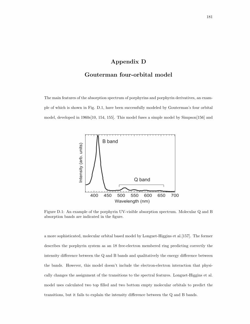
181
Appendix D
Gouterman four-orbital model
The main features of the absorption spectrum of porphyrins and porphyrin derivatives, an exam-
ple of which is shown in Fig. D.1, have been successfully modeled by Gouterman’s four orbital
model, developed in 1960s[10, 154, 155]. This model fuses a simple model by Simpson[156] and
Inte
nsity (
arb
. units)
700650600550500450400
Wavelength (nm)
B band
Q band
Figure D.1: An example of the porphyrin UV-visible absorption spectrum. Molecular Q and Babsorption bands are indicated in the figure.
a more sophisticated, molecular orbital based model by Longuet-Higgins et al.[157]. The former
describes the porphyrin system as an 18 free-electron membered ring predicting correctly the
intensity difference between the Q and B bands and qualitatively the energy difference between
the bands. However, this model doesn’t include the electron-electron interaction that physi-
cally changes the assignment of the transitions to the spectral features. Longuet-Higgins et al.
model uses calculated two top filled and two bottom empty molecular orbitals to predict the
transitions, but it fails to explain the intensity difference between the Q and B bands.
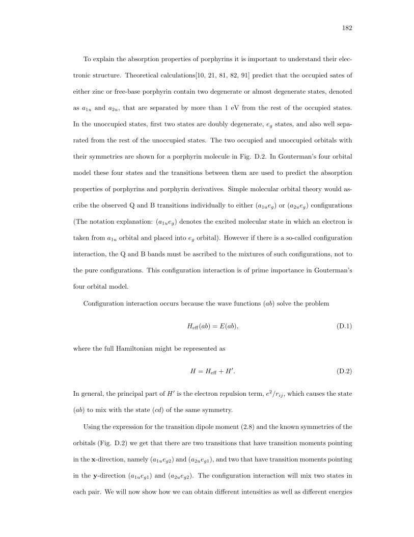
182
To explain the absorption properties of porphyrins it is important to understand their elec-
tronic structure. Theoretical calculations[10, 21, 81, 82, 91] predict that the occupied sates of
either zinc or free-base porphyrin contain two degenerate or almost degenerate states, denoted
as a1u and a2u, that are separated by more than 1 eV from the rest of the occupied states.
In the unoccupied states, first two states are doubly degenerate, eg states, and also well sepa-
rated from the rest of the unoccupied states. The two occupied and unoccupied orbitals with
their symmetries are shown for a porphyrin molecule in Fig. D.2. In Gouterman’s four orbital
model these four states and the transitions between them are used to predict the absorption
properties of porphyrins and porphyrin derivatives. Simple molecular orbital theory would as-
cribe the observed Q and B transitions individually to either (a1ueg) or (a2ueg) configurations
(The notation explanation: (a1ueg) denotes the excited molecular state in which an electron is
taken from a1u orbital and placed into eg orbital). However if there is a so-called configuration
interaction, the Q and B bands must be ascribed to the mixtures of such configurations, not to
the pure configurations. This configuration interaction is of prime importance in Gouterman’s
four orbital model.
Configuration interaction occurs because the wave functions (ab) solve the problem
Heff(ab) = E(ab), (D.1)
where the full Hamiltonian might be represented as
H = Heff +H ′. (D.2)
In general, the principal part of H ′ is the electron repulsion term, e2/rij , which causes the state
(ab) to mix with the state (cd) of the same symmetry.
Using the expression for the transition dipole moment (2.8) and the known symmetries of the
orbitals (Fig. D.2) we get that there are two transitions that have transition moments pointing
in the x-direction, namely (a1ueg2) and (a2ueg1), and two that have transition moments pointing
in the y-direction (a1ueg1) and (a2ueg2). The configuration interaction will mix two states in
each pair. We will now show how we can obtain different intensities as well as different energies
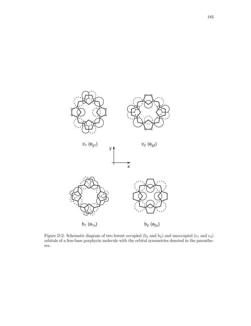
183
x
yc2 (eg2)c1 (eg1)
b2 (a2u)b1 (a1u)
Figure D.2: Schematic diagram of two lowest occupied (b1 and b2) and unoccupied (c1 and c2)orbitals of a free-base porphyrin molecule with the orbital symmetries denoted in the parenthe-ses.

184
for B and Q bands, for the states with the transition dipole moment in the y-direction. For the
other direction, the derivation is identical.
Let’s define
E1 = 12 (E(a2ueg2) + E(a1ueg1))
E2 = 12 (E(a2ueg2)− E(a1ueg1))
E0 =∫(a1ueg1)H(a2ueg2)dv,
(D.3)
where energy E0 represents the configuration interaction. The Hamiltonian in the basis set of
the mixed states
B0y =
√2((a2ueg2) + (a1ueg1))
Q0y =
√2((a2ueg2)− (a1ueg1))
(D.4)
is then given as E1 + E0 E2
E2 E1 − E0
.
This matrix can be diagonalized in the new basis set of By and Qy states that are linear
combination of B0y and Q0
y states
By = cos νB0y + sin νQ0
y
Qy = − sin νB0y + cos νQ0
y,
(D.5)
where tan ν = E2/E0. These mixed configurations, By and Qy together with the mixed configu-
rations in the x-direction (Bx and Qx) contribute to the porphyrin B and Q bands, respectively.
In the limit of ν ≪ 1, or when the energy separation between two configurations (a1ueg1) and
(a2ueg2), E2, is small, mixed configurations can be approximated by
By = B0y + νQ0
y
Qy = −νB0y +Q0
y.
(D.6)
This limit of small ν is valid in case of both ZnTPP and H2TPP molecules, since the top two
occupied states as well as bottom two unoccupied states are degenerate or nearly degenerate and
it is expected that the energy of configuration (a1ueg1) is close to the energy of configuration
(a2ueg2).
185
Furthermore, the final energies of these mixed configurations for ν ≪ 1 are given by
E(By) = E1 + E0(1 + 2ν2)
E(Qy) = E1 − E0(1 + 2ν2).
(D.7)
The energy of the mixed state By is larger than the energy of the mixed state Qy meaning that
the B, or Soret band will appear at shorter and Q band at longer wavelength.
The intensities of Q and B bands are mostly determined by the transition dipole moments of
the corresponding transitions. For the mixed states, transition dipole moments can be calculated
from the transition dipole moment between two starting, not mixed molecular orbitals. This
transition dipole moment is defined as
R(ab) =√2∑i
caicbiri, (D.8)
where (ab) denotes a transition between two molecular orbitals, cai and cbi are the molecular
orbital coefficients on an atom i in the orbitals a and b respectively and ri is the position vector
of the ith atom.
The transition dipole moments of the mixed states By and Qy are pointing in y-direction
and for small ν are given by
Ry(By) = (R2 − ν2R2 + 2νRr)1/2
Ry(Qy) = νR− r,
(D.9)
where R = (R1 + R2)/√2 and r = (R2 − R1)/
√2. R1 and R2 are the dipole moments of
the transitions (a1ueg1) and (a2ueg2), respectively. For both ZnTPP and H2TPP, it can be
calculated that R1 ≈ R2. This means that R will be much larger than r in the expression (D.9).
Since both r and ν are small, to the first approximation Ry(By) will be given by R, whereas
Ry(Qy) will be much smaller than R. The same result can be obtained for Rx(Bx) and Rx(Qx).
This means that the B band will be much more intense than Q band in the spectrum, which is
indeed the main characteristics of the porphyrin UV-visible spectrum.
We have previously mentioned the differences between the absorption spectra of ZnTPP and
H2TPP, especially observed in the Q band region (Fig. 2.13). For ZnTPP molecule, Q band
186
consists of two peaks, Q(0,0) and Q(0,1) corresponding to the transition to two different vibronic
levels of the molecule. Since the ZnTPP molecule has a four-fold symmetry, the contributions
to the Q band in x and y directions (Qx and Qy) are degenerate. Q(0,0) and Q(0,1) peaks
thus both consist of two degenerate peaks. In H2TPP molecule four-fold symmetry is broken by
insertion of two hydrogen atoms instead of zinc atom and the two-fold symmetry is established.
x and y directions are no longer equivalent and the degeneracy between Qx and Qy is lifted.
Each of the Q band peaks is split in two, giving rise to four peaks, Qx(0, 0), Qx(0, 1), Qy(0, 0)
and Qy(0, 1) in total. Similar splitting of the peaks is observed in the B band region for H2TPP
molecule, but the splitting is much smaller than for Q band.
187
Appendix E
Molecular orientation determination using NEXAFS
In addition to the electronic structure, NEXAFS can reveal information about the orientation
of the molecules adsorbed on the surface of the sample. For that, the angle of incidence of
linearly polarized synchrotron X-ray radiation is gradually changed and NEXAFS spectrum for
each incident angle is recorded. Since bonds and the associated molecular orbitals are highly
directional, NEXAFS cross section as well as the intensity of NEXAFS resonances will strongly
depend on the angle of incident radiation.
The photoabsorption cross section has been previously calculated for the UPS process (Eq.
(2.5)) and it is identical in case of NEXAFS. The central quantity in the photoabsorption cross
section is the transition dipole moment M given by Eq. (2.7). Transition dipole moment is
thus proportional to
M ∝ ⟨Ψf |r|Ψi⟩, (E.1)
where Ψi and Ψf are the initial and final electron states, and r is the position vector operator.
Intensity of the NEXAFS features is directly proportional to the photoabsorption cross
section and it will follow the same dependence on the angle between the incident electric field
and the transition dipole moment, given by Eq. (2.5). Intensity of NEXAFS features is, thus
proportional to
I ∝ |ϵ ·M|2 , (E.2)
where ϵ is the polarization direction of the electric field.
To obtain the dependence of the intensity of NEXAFS features on the incident angle of the
electric field, the transition dipole moment M needs to be determined for a particular NEXAFS
188
transition. We will limit our discussion to the transitions from 1s sate, i.e. K-edge, because
these transitions are the most important for low-Z atoms, carbon and nitrogen in our case,
found in the organic molecules.
The initial 1s state is spherically symmetric and to a very good approximation represented
by the atomic 1s wavefunction of the excited atom in a molecule, Ψi = R1s(r). A final excited
state of an electron is a molecular bound state that can be represented by a linear combination
of the atomic orbitals (LCAO) on the excited atom. For the second row atoms (carbon, nitrogen
and oxygen) the excited state is well represented by a linear combination of 2s and 2p orbitals,
so the final state wave function can be written as
Ψf = aΨ2s + bΨ2px + cΨ2py + dΨ2pz . (E.3)
If the wave functions in LCAO expansion are written explicitly in the spherical coordinates, the
final state is given by
Ψf = aR2s(r) +R2p(r)(b sin θ cosϕ+ c sin θ sinϕ+ d cos θ), (E.4)
where a, b, c and d represent the weights of a particular atomic orbital in the LCAO expansion,
and R2s(r) and R2p(r) are the radial atomic wave functions.
We can now express the position vector r in spherical coordinates and do the integration to
obtain the transition dipole matrix element (Eq. (E.1)) as[73]
M = R4π
3(bx+ cy + dz), (E.5)
where R is the radial dipole matrix element and it is given by
R =
∫R1s(r)R2p(r)r
3dr (E.6)
and x, y and z are the unit vectors along the coordinate system axes. At this point it is useful to
calculate the, so-called direction of the largest amplitude of the final state orbital. This vector,
denoted by O points in the direction bx + cy + dz for this particular final state given by Eq.
(E.4). The direction of the vector O is, thus, determined by the superposition of the directions

189
of the three 2p orbitals in the LCAO expansion. Transition dipole moment can now be written
as
M = R4π
3O. (E.7)
The transition dipole moment points, thus in the same direction as the vector of the largest
amplitude O for a particular final state orbital on the excited atom. Furthermore, this direction
coincides with the p orbital component of the final state. For example, if an electron is excited
from 1s to π∗ molecular orbital, that is composed of the pz atomic orbitals, the vector of the
largest amplitude O, and the transition dipole moment M will point in z direction.
Using expression E.2, the angular dependence of the NEXAFS intensity is given by
I ∝ |ϵ ·M|2 ∝ |ϵ ·O|2 ∝ cos2 δ, (E.8)
where δ is the angle between the direction of the largest amplitude of the final state orbital O
and the electric field polarization vector ϵ. The intensity of a particular NEXAFS resonance
will, thus be maximal when the electric field polarization vector is parallel to the direction of
the largest amplitude of that particular final state orbital. From this angular dependence in
NEXAFS, the orientation of the molecules adsorbed at surfaces can be deduced.
As an example, the case of benzene molecule lying flat on Ag(110) surface is shown in Fig.
E.1. Benzene molecule consists of six carbon atoms arranged in a hexagon with single and
double bonds alternating between them. Using the coordinate system denoted in the figure,
the unoccupied π∗ orbital lies perpendicular to the molecular plane and it consists of pz carbon
atom orbitals. Unoccupied σ∗ orbital, however, lies in the molecular plane and consists of
sp2 hybridized orbitals, where p orbitals involved in hybridization are px and py carbon atom
orbitals. For π∗ orbital, the vector of largest amplitude, thus points in z direction, whereas for
σ∗ orbital it lies in x-y plane, perpendicular to z direction.
In Fig. E.1, carbon K-edge NEXAFS spectrum for two different incident angles is shown, for
grazing and 90 angles with respect to the Ag(110) surface. As the incident angle changes, the
intensities of π∗ and σ∗ resonances in the spectrum change, however they change in a different

190
in-plane
out-of-plane
xy
z
Benzene molecular orbitals
C 1s
π∗
σ∗
8
4
0
π1
∗
π2
∗
8
4
0
σ1
∗
σ2
∗
Norm
aliz
ed Inte
nsity
275 285 295 305 315 325
Photon Energy (eV)
Lying-down benzene on Ag (110)
E
E
Figure E.1: Carbon K-edge NEXAFS spectra of the benzene molecule adsorbed on Ag (110)surface recorded under both grazing and normal X-ray incidence angles.
way. The intensity of the π∗ resonances is maximal when the incident radiation is coming
under grazing angle with respect to the surface of the sample (Fig. E.1), since in that case
the polarization vector of the electric field is parallel to the largest amplitude of direction of
π∗ orbital, that points in z direction. When the radiation is coming normal to the surface of
the sample, the electric field is perpendicular to the direction of the largest amplitude of the π∗
orbital and the intensity of the π∗ resonance vanishes (Eq. (E.8)).
The intensity dependence of σ∗ NEXAFS resonance on the incoming angle is opposite. When
the radiation comes under grazing angle, the intensity of the feature is low (Fig. E.1), since the
electric field is perpendicular to the largest amplitude direction of the σ∗ orbital, that lies in x-y
plane. When the incoming radiation is normal to the surface of the sample, the electric field is
parallel to the largest amplitude direction of the σ∗ orbital and the intensity of the NEXAFS
σ∗ related features is maximal (Eq. (E.8)). From this behavior, the orientation of the molecule
can be clearly deduced. In this case, benzene molecule lies flat on the Ag(110) surface.
To extract quantitative information on the orientation of bonds, spectra recorded at different

191
angles of incidence need to be normalized to the flux of the incoming photons and to the
ionization threshold height. In principle, the tilt angle of a molecular orbital can then be
found by determining the intensity of the corresponding resonance as a function of the angle
of incidence of the photons. In case of the molecules with π bonds, the large and narrow π∗
resonances are most suitable for quantitative evaluation of the angular dependence because of
it’s clear separation from the ionization edge and absence of any interfering background. It
is also worth noting that the X-ray beam spot in NEXAFS is macroscopic, so the obtained
tilt angle will present an average over a macroscopic region on the sample. In order to have
a definite molecular orientation measured, molecules thus need to be ordered on macroscopic
length scales comparable to the X-ray beam spot dimensions.
Oα
θ
δ
x
y
z, N
ε
Figure E.2: Angles considered in the derivation of the angular dependance of the NEXAFSintensity.
It is important to note that at a particular tilt angle of the molecule with respect to the
surface of the sample, called the “magic angle” the NEXAFS intensity will be independent on
the incidence angle of X-ray radiation. This can be derived using Eq. (E.8). The angle δ in
this equation can be written in terms of the angle θ between the electric field polarization ϵ and
the normal of the sample, and angle α between vector O and the normal of the sample (for the
reference on angles, see Fig. E.2). The expression for NEXAFS intensity in terms of angles θ

192
and α is given as[73]
I ∝ 1
3
(1 +
1
2(3 cos2 θ − 1)(3 cos2 α− 1)
). (E.9)
The angle α is also the molecular tilt angle, i.e. the angle between the plane of the molecule
and the surface of the sample. The dependance on the tilt angle α enters the equation as the
second Legendre polynomial, i.e. (3 cos2 α− 1). It is clear now that when α is equal to the zero
of that polynomial, an angle called the “magic angle” θm ≈ 54.7, the NEXAFS intensity will
be independent on the incident angle of the electric field. If all molecules are, thus tilted under
this angle, NEXAFS will not be able to distinguish this arrangement from randomly oriented
molecules.

193
Appendix F
Density functional theory basics and basis sets
In the next few sections we will first briefly explain Hartree and Hartree-Fock approximations to
establish the understanding of basic energy terms that contribute to the total energy of a many-
body system in general. Furthermore, we will introduce the basic ideas of density functional
theory (DFT) and shortly explain the functionals and the basis sets used in our calculations.
F.1 The many-body problem
The behavior of electrons and ions in a molecule or a solid is described by a many-body
Schrodinger equation
HΨ(RI, ri) = EΨ(RI, ri), (F.1)
where Ψ(RI, ri) is the many-body wave function, that depends on the positions of all
ions RI and positions of all electrons ri and H is the hamiltonian of the system. This
many-body hamiltonian is given by
H = Te + TI +Wee +WeI +WII , (F.2)
where Te and TI are the kinetic energies of electrons and ions respectively, Wee is the electron-
electron interaction term, WeI is the electron-ion interaction term and WII term accounts for
the interaction between ions in the system.
Typically, we can think of ions as moving slowly in space and electrons responding instan-
taneously to any ionic motion so that the many-body wave function Ψ(RI, ri) explicitly
depends only on electronic degrees of freedom, i.e. Ψ(ri) . This approximation is known as
Born-Oppenheimer approximation. We can then omit the quantum mechanical term for kinetic
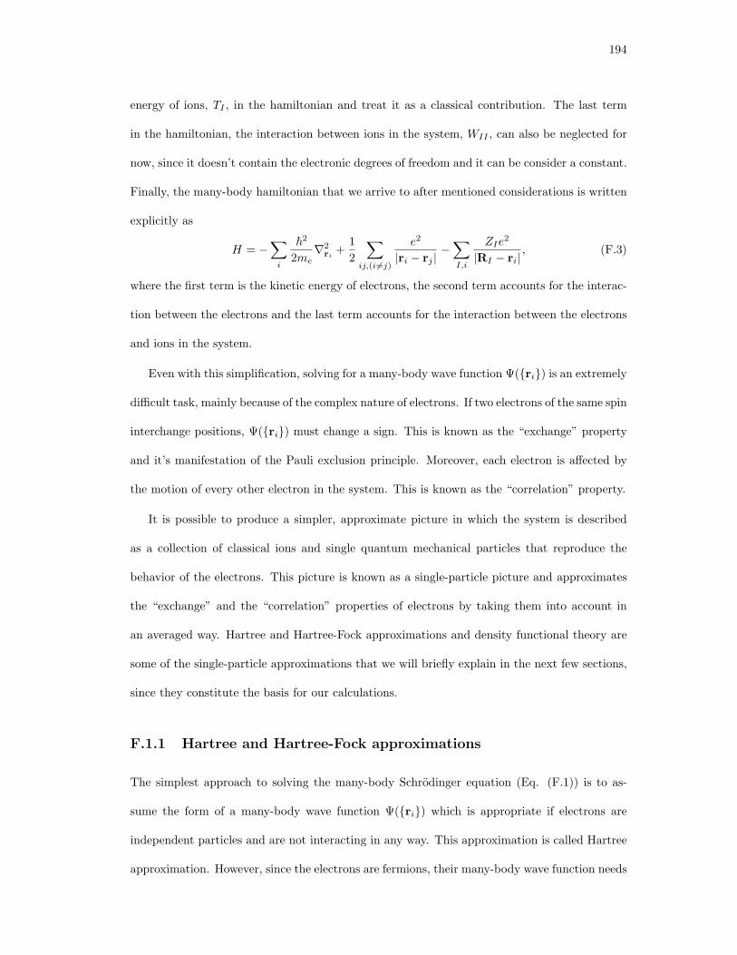
194
energy of ions, TI , in the hamiltonian and treat it as a classical contribution. The last term
in the hamiltonian, the interaction between ions in the system, WII , can also be neglected for
now, since it doesn’t contain the electronic degrees of freedom and it can be consider a constant.
Finally, the many-body hamiltonian that we arrive to after mentioned considerations is written
explicitly as
H = −∑i
~2
2me∇2
ri +1
2
∑ij,(i =j)
e2
|ri − rj |−
∑I,i
ZIe2
|RI − ri|, (F.3)
where the first term is the kinetic energy of electrons, the second term accounts for the interac-
tion between the electrons and the last term accounts for the interaction between the electrons
and ions in the system.
Even with this simplification, solving for a many-body wave function Ψ(ri) is an extremely
difficult task, mainly because of the complex nature of electrons. If two electrons of the same spin
interchange positions, Ψ(ri) must change a sign. This is known as the “exchange” property
and it’s manifestation of the Pauli exclusion principle. Moreover, each electron is affected by
the motion of every other electron in the system. This is known as the “correlation” property.
It is possible to produce a simpler, approximate picture in which the system is described
as a collection of classical ions and single quantum mechanical particles that reproduce the
behavior of the electrons. This picture is known as a single-particle picture and approximates
the “exchange” and the “correlation” properties of electrons by taking them into account in
an averaged way. Hartree and Hartree-Fock approximations and density functional theory are
some of the single-particle approximations that we will briefly explain in the next few sections,
since they constitute the basis for our calculations.
F.1.1 Hartree and Hartree-Fock approximations
The simplest approach to solving the many-body Schrodinger equation (Eq. (F.1)) is to as-
sume the form of a many-body wave function Ψ(ri) which is appropriate if electrons are
independent particles and are not interacting in any way. This approximation is called Hartree
approximation. However, since the electrons are fermions, their many-body wave function needs
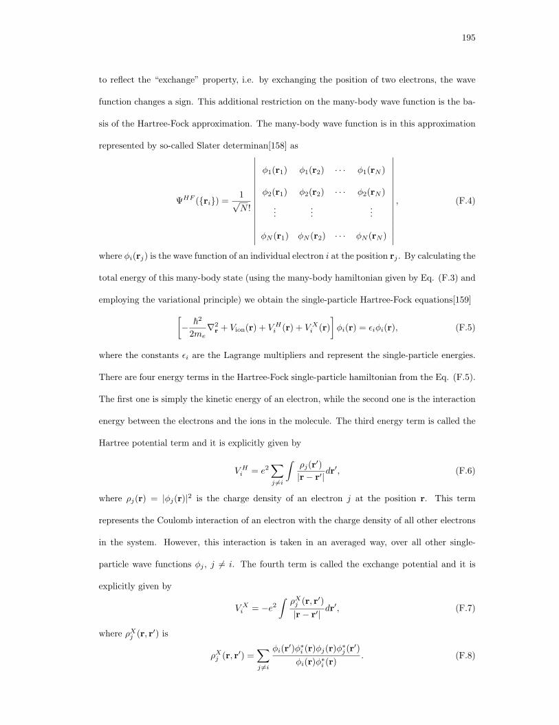
195
to reflect the “exchange” property, i.e. by exchanging the position of two electrons, the wave
function changes a sign. This additional restriction on the many-body wave function is the ba-
sis of the Hartree-Fock approximation. The many-body wave function is in this approximation
represented by so-called Slater determinan[158] as
ΨHF (ri) =1√N !
∣∣∣∣∣∣∣∣∣∣∣∣∣∣∣∣
ϕ1(r1) ϕ1(r2) · · · ϕ1(rN )
ϕ2(r1) ϕ2(r2) · · · ϕ2(rN )
......
...
ϕN (r1) ϕN (r2) · · · ϕN (rN )
∣∣∣∣∣∣∣∣∣∣∣∣∣∣∣∣, (F.4)
where ϕi(rj) is the wave function of an individual electron i at the position rj . By calculating the
total energy of this many-body state (using the many-body hamiltonian given by Eq. (F.3) and
employing the variational principle) we obtain the single-particle Hartree-Fock equations[159][− ~2
2me∇2
r + Vion(r) + V Hi (r) + V X
i (r)
]ϕi(r) = ϵiϕi(r), (F.5)
where the constants ϵi are the Lagrange multipliers and represent the single-particle energies.
There are four energy terms in the Hartree-Fock single-particle hamiltonian from the Eq. (F.5).
The first one is simply the kinetic energy of an electron, while the second one is the interaction
energy between the electrons and the ions in the molecule. The third energy term is called the
Hartree potential term and it is explicitly given by
V Hi = e2
∑j =i
∫ρj(r
′)
|r− r′|dr′, (F.6)
where ρj(r) = |ϕj(r)|2 is the charge density of an electron j at the position r. This term
represents the Coulomb interaction of an electron with the charge density of all other electrons
in the system. However, this interaction is taken in an averaged way, over all other single-
particle wave functions ϕj , j = i. The fourth term is called the exchange potential and it is
explicitly given by
V Xi = −e2
∫ρXj (r, r′)
|r− r′|dr′, (F.7)
where ρXj (r, r′) is
ρXj (r, r′) =∑j =i
ϕi(r′)ϕ∗
i (r)ϕj(r)ϕ∗j (r
′)
ϕi(r)ϕ∗i (r)
. (F.8)
196
This term originates from the “exchange” property of the many-body wave function that we
included in it by a construction. In other words, if we only employed the Hartree approximation,
this term would not be present in the single-particle equations.
Finally, it is important to note that the Hartree-Fock equations are self-consistent. This
means that the solutions of these equations, the single-particle wave functions ϕi, enter the
same equations as a part of Hartree (Eq. (F.6)) and exchange potentials (Eq. (F.7)). Each
single-particle wave function ϕi can then be calculated iteratively, which is easily implemented
as a part of a computer algorithm.
F.1.2 Density Functional Theory
In a series of seminal papers Hohenberg, Kohn and Sham developed a different way of looking
at the many-body problem, which has been called Density Functional Theory (DFT). The basic
ideas of DFT are contained in two original papers of Hohenberg, Kohn and Sham[160, 161]
and are referred to as the Hohenberg-Kohn-Sham theorems. The theory has had a tremendous
impact on the calculations of the properties of molecules and solids.
The basic concept is that instead of dealing with the many-body Schrodinger equation (Eq.
(F.1)) which involves many-body wave function Ψ(ri), one deals with the formulation of the
problem that involves a total density of electrons n(r). This considerably simplifies the calcula-
tion since the many-body wave function need not to be explicitly specified, as was done in the
Hartree and Hartree-Fock approximations. Thus, instead of starting with a drastic approxima-
tion for the behavior of the system (which is what Hartree and Hartree-Fock wave functions
represent), one can develop the appropriate single-particle equations in an exact manner and
then introduce approximations as needed.
In the next few paragraphs we will mention two theorems and their consequences that are
the basis of DFT. The proofs of these theorems can be found somewhere else[159].
As mentioned before, there are three parts of the many-body hamiltonian (Eq. (F.3)); the
kinetic energy of electrons (T), electron-electron interaction (W) and electron-ion interaction,

197
also referred to as the external potential V(r).
The first theorem, called Hohenberg-Kohn theorem states that for a given external, ionic,
potential V(r) there is only one density of electrons n(r) corresponding to that external potential
and vice versa. There is, thus, a one-to-one correspondence between the external potential and
the electron density.
Let’s focus on two other terms in the hamiltonian, namely the kinetic energy and the
electron-electron interaction terms. The expression
F [n(r)] = ⟨Ψ|T +W |Ψ⟩ (F.9)
must be a universal functional of the density, since both energy terms are common to all solids.
Therefore, this functional does not depend on anything else other than the electron density,
which is, however, uniquely determined by the external potential V(r) that differs from a system
to a system. From this we conclude that the total energy of the system is a functional of the
density n(r) and is given by
E[n(r)] = F [n(r)] +
∫V (r)n(r)dr. (F.10)
The second theorem, called Kohn-Sham theorem states that the electron density n(r) corre-
sponding to the external potential V(r) is the one that will minimize the total energy functional
E[(n(r))] (Eq. (F.10)) and it will, thus, represent the ground state density of the system.
Now we need to obtain a set of single-particle equations, just as we did before in Hartree
and Hartree-Fock approximations. The important difference in this case is that we don’t have
to interpret these single-particle states as the ones corresponding to the electrons in the system.
They can represent fictitious particles with the only requirement that their density is identical
to the density of real electrons. Furthermore, we can choose that these particles are non-
interacting, so that the many-body wave function is a Slater determinant of single-particle wave
functions (Eq. (F.4)), which considerably simplifies the calculations. The functional F[n(r)] is
now given by[159]
F [n(r)] = TS [n(r)] +e2
2
∫ ∫n(r)n(r′)
|r− r′|drdr′ + EXC [n(r)], (F.11)

198
where the first term is the kinetic energy of the states in the Slater determinant. Since the
fictitious particles are non-interacting this term takes a simple form and it is given by
TS [n(r)] =∑i
⟨ϕi| −~2
2me∇2
r|ϕi⟩. (F.12)
The second term in the functional F[n(r)] (Eq. (F.11)) is the Coulomb interaction, which
we separate out from the total electron-electron interaction term in F[n(r)]. By the defini-
tion, everything else that is left is called exchange-correlation energy and it is denoted by
EXC [n(r)]. This term includes all the effects of the many-body character of the electron sys-
tem that are treated separately. By employing the variational principle on the total energy
functional, E[n(r)], with the restriction that the total number of particles does not change, we
arrive at, so-called Kohn-Sham single-particle equations[159]
[− ~2
2me∇2
r + V eff(r, n(r))
]ϕi(r) = ϵiϕi(r), (F.13)
where the effective potential, V eff(r, n(r)), is given by
V eff(r, n(r)) = V (r) + e2∫
n(r′)
|r− r′|dr′ +
δEXC [n(r)]
δn(r), (F.14)
with V(r) denoting the external potential due to ions in the molecule and the last term is the
variational derivative of a yet unspecified functional EXC [n(r)]. The single-particle orbitals,
ϕi(r) in the Eq. (F.13) are referred to Kohn-Sham orbitals. These equations are, again, self-
consistent and are solved iteratively, which is easily implemented in the computer algorithm.
It is important to note that Kohn-Sham equations are exact, there was no approximations
that were done to obtain them, contrary to Hartree and Hartree-Fock equations. However, the
approximation that needs to be done is for the exchange-correlation functional EXC [n(r)] that
was so far left to unspecified. The question of choosing the right exchange-correlation functional
that captures all the many-body effects of the electron-electron interaction is the “holy grail” in
the DFT calculations. In the past several decades many exchange-correlation functionals have
been developed. There are set of exchange-correlation functionals that depend on the density
locally[162, 163], i.e. the density needs to be evaluated at one point in space. Usually, these
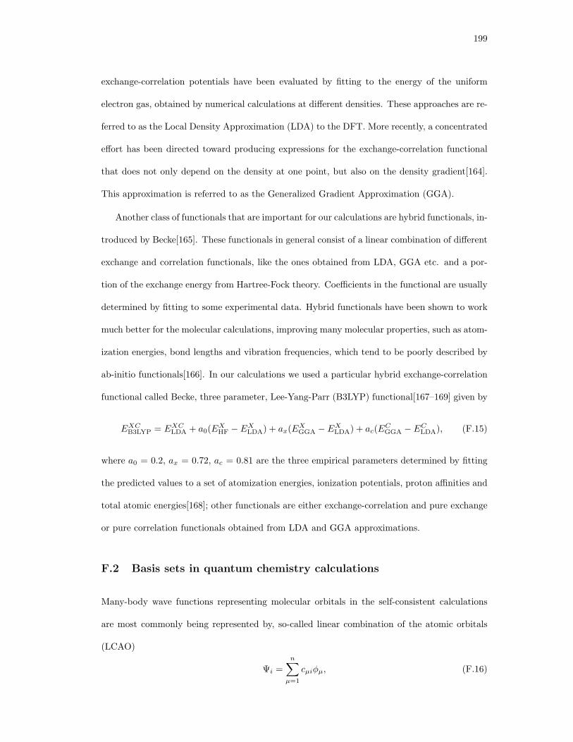
199
exchange-correlation potentials have been evaluated by fitting to the energy of the uniform
electron gas, obtained by numerical calculations at different densities. These approaches are re-
ferred to as the Local Density Approximation (LDA) to the DFT. More recently, a concentrated
effort has been directed toward producing expressions for the exchange-correlation functional
that does not only depend on the density at one point, but also on the density gradient[164].
This approximation is referred to as the Generalized Gradient Approximation (GGA).
Another class of functionals that are important for our calculations are hybrid functionals, in-
troduced by Becke[165]. These functionals in general consist of a linear combination of different
exchange and correlation functionals, like the ones obtained from LDA, GGA etc. and a por-
tion of the exchange energy from Hartree-Fock theory. Coefficients in the functional are usually
determined by fitting to some experimental data. Hybrid functionals have been shown to work
much better for the molecular calculations, improving many molecular properties, such as atom-
ization energies, bond lengths and vibration frequencies, which tend to be poorly described by
ab-initio functionals[166]. In our calculations we used a particular hybrid exchange-correlation
functional called Becke, three parameter, Lee-Yang-Parr (B3LYP) functional[167–169] given by
EXCB3LYP = EXC
LDA + a0(EXHF − EX
LDA) + ax(EXGGA − EX
LDA) + ac(ECGGA − EC
LDA), (F.15)
where a0 = 0.2, ax = 0.72, ac = 0.81 are the three empirical parameters determined by fitting
the predicted values to a set of atomization energies, ionization potentials, proton affinities and
total atomic energies[168]; other functionals are either exchange-correlation and pure exchange
or pure correlation functionals obtained from LDA and GGA approximations.
F.2 Basis sets in quantum chemistry calculations
Many-body wave functions representing molecular orbitals in the self-consistent calculations
are most commonly being represented by, so-called linear combination of the atomic orbitals
(LCAO)
Ψi =n∑
µ=1
cµiϕµ, (F.16)
200
where Ψi is ith molecular orbital, cµi are the expansion coefficients, ϕµ is µth atomic orbital and
n is the total number of the atomic orbitals in the expansion. Strictly speaking, ϕµ are rather
called the basis functions instead of the atomic orbitals, since some approximative functions
and not the atomic orbitals themselves are most often used in the expansion.
In early days, Slater Type Orbitals (STOs)[170] were used as basis functions due to their
similarity to atomic orbitals of the hydrogen atom. Slater type orbitals are given by
χSTOnlm = Nrn−1e−ζrY m
l (θ, ϕ), (F.17)
where N is normalization constant, ζ is called the exponent, Y ml (θ, ϕ) are the spherical har-
monics that describe the angular dependency of the STO, while n, l and m are the quantum
numbers.
However, STO functions are not suitable for fast evaluation of one and two-electron integrals
in the self-consistent calculations. This is why Gaussian Type Orbitals (GTO), or so-called
Gaussian primitives were introduced. These functions are given by
χGTO = Ne−αr2xlymzn, (F.18)
where N is a normalization constant, α is called the exponent; x, y and z are the Cartesian
coordinates while l, m and n are the exponents of the cartesian coordinates. Each STO function
can be approximated by a sum of several Gaussian primitives with different coefficients and
exponents α. Even if the number of the basis functions is effectively increased in case when
Gaussian primitives are used, one and two-electron integrals will be calculated much faster than
in the case if the STO functions are used.
The main difference between STO and GTO functions is that the preexponential factor rn−1
in STO functions is dropped, the radial coordinate r in the exponential function is squared, so
that the dependence is not exp(−ζr) but exp(−αr2) and the angular momentum part is replaced
by a simple function of Cartesian coordinates. The absence of the preexponential factor rn−1
restricts Gaussian primitives to approximating only 1s, 2p, 3d, 4f etc. orbitals. This was
done for practical reasons, i.e. for fast integral calculations. However, linear combinations of

201
Gaussians are able to approximate the correct nodal properties of the atomic orbitals by taking
coefficients with different signs in the sum.
Nowadays, there are numerous basis sets used in quantum chemistry. The simplest basis
set is a minimal basis set, where one STO basis function is attributed to one atomic orbital on
each atom. For example, for carbon atom there will be one STO orbital for each 1s, 2s, 2px,
2py and 2pz atomic orbital, which gives five basis functions in total. Each STO function can be
approximated by a varying number of Gaussian primitives.
The main disadvantage of the minimal basis set is the lack of its flexibility. For a given
atom, the shape of an STO orbital is always the same, no matter its environment. We expect,
however, that depending on the molecular environment, atomic orbitals will be distorted, they
will either radially extend or contract or polarize due to the presence of other atoms. To account
for these distortions additional basis functions are added to the basis set.
In a, so-called double-zeta basis set, a percentage of an additional STO function with a
different ζ exponent is added to the existing STO function to account for different spatial
extent of the orbital. If an STO function with larger ζ exponent is added, the overall orbital
will be contracted radially and if an STO function with smaller ζ exponent is added, the final
orbital will be radially more extended.
In our calculations we used, so-called, split-valence basis set, where minimal basis set has
been used for core orbitals and double-zeta basis set for valence orbitals. Different treatment
of core and valence orbitals is justified by the fact that the valence orbitals, which contribute
to the bonding, will be more affected by other atoms in the molecule compared to the core
orbitals. To account for these changes, more flexibility is needed for the valence than for the
core orbitals. Out of many different split-valence basis sets, we used 6-31G basis set, that exists
for atoms from H to Zn[171, 172]. The basis set notation, 6-31G, is telling us about the number
of Gaussian primitives that have been used to approximate each STO basis function. Each
core STO basis function in 6-31G basis set is approximated by 6 Gaussian primitives, while
two valence STO functions are approximated by 3 and 1 Gaussian primitive respectively. For

202
a carbon atom, for example, this basis set will consist of one STO basis function for 1s orbital
and two STO basis functions for each 2s, 2px, 2py and 2pz orbital, which gives nine STO basis
functions in total.
The effects of orbital polarization and anisotropic distortion due to the presence of other
atoms in the molecule can be accounted for by adding basis functions with higher angular
momentum to the basis set. Usually, asterisk signs are used to denote that the polarization
functions have been added to the basis set. For example, in the 6-31G* basis set additional
d-type function is added for atoms from Li to Ca and f-type function for atoms from Sc to
Zn[97, 98, 173]. In the 6-31G** basis set on top of added d-type functions for atoms from
Li and Ca and f-type functions from Sc to Zn atoms, p-type functions are added to hydrogen
atoms as well[173]. Results obtained by adding polarization functions to the split-valence basis
sets are a significant improvement, particularly for the accurate determination of bond angles.
Calculations presented in this thesis were done with either 6-31G* or 6-31G** basis sets
obtained from the online basis set library (EMSL Basis Set Exchange 1) or directly from the
GAMESS software package library.
1https://bse.pnl.gov/bse/portal

Vita
Senia Coh
Education
2006-2012 Rutgers University, New Brunswick, NJPh.D. in Physics
1998-2001 University of Zagreb, CroatiaB.Sc. in Physics
Positions held
2006-2011 Rutgers-Lucent FellowPhysics and Astronomy Department at Rutgers University
2011-2012 Graduate AssistantPhysics and Astronomy Department at Rutgers University
Publications
Senia Coh, Sylvie Rangan, Robert Allen Bartynski, Keyur Chitre and Elena Galoppini, ”Elec-tronic structure and energy level alignment of zinc and free-base tetracarboxyphenylporphyrinderivatives on ZnO(1120) single crystal surface”, in preparation
Sylvie Rangan, Senia Coh, Robert Allen Bartynski, Johnathan Rochford and Elena Galoppini,”Energy alignment, molecular packing and electronic pathways: zinc(II) tetraphenylporphyrinderivatives adsorbed on TiO2(110) and ZnO(1120) surfaces”, submitted to Journal of AmericanChemical Society
Sylvie Rangan, Senia Katalinic, Ryan Thorpe, Robert Allen Bartynski, Johnathan Rochfordand Elena Galoppini, ”Energy Level Alignment of a Zinc(II) Tetraphenylporphyrin Dye Ad-sorbed onto TiO2(110) and ZnO(1120) Surfaces”, Journal of Physical Chemistry C, 114, 1139(2010)
Leszek S. Wielunski, S. Katalinic, B. Lee, M. Connors, E. Garfunkel, L. C. Feldman and V.Podzorov, ”Ion-scattering analysis of self-assembled monolayers of silanes on organic semicon-ductors”, Nuclear Instruments and Methods in Physics Research B, 268, 1889 (2010)