electronics b - massachusetts institute of technology
TRANSCRIPT

JV: 2.372J/6.777J Spring 2007, Lecture 7E - 1
Cite as: Joel Voldman, course materials for 6.777J / 2.372J Design and Fabrication of Microelectromechanical Devices, Spring 2007. MIT OpenCourseWare (http://ocw.mit.edu/), Massachusetts Institute of Technology. Downloaded on [DD Month YYYY].
Electronics B
Joel Voldman
Massachusetts Institute of Technology

JV: 2.372J/6.777J Spring 2007, Lecture 7E - 2
Cite as: Joel Voldman, course materials for 6.777J / 2.372J Design and Fabrication of Microelectromechanical Devices, Spring 2007. MIT OpenCourseWare (http://ocw.mit.edu/), Massachusetts Institute of Technology. Downloaded on [DD Month YYYY].
Outline> Elements of circuit analysis
> Elements of semiconductor physics• Semiconductor diodes and resistors• The MOSFET and the MOSFET inverter/amplifier
> Op-ampsTODAY

JV: 2.372J/6.777J Spring 2007, Lecture 7E - 3
Cite as: Joel Voldman, course materials for 6.777J / 2.372J Design and Fabrication of Microelectromechanical Devices, Spring 2007. MIT OpenCourseWare (http://ocw.mit.edu/), Massachusetts Institute of Technology. Downloaded on [DD Month YYYY].
Elements of semiconductor physics> Discrete molecules (e.g., hydrogen
atom) have discrete energy levels that the electrons can occupy
• Determined via quantum mechanics
> Adding a discrete amount of energy to the electrons (via light, thermal energy, etc.) can excite an electron from its ground state to an excited state
> Different atoms have different number of filled states
• All the action typically happens at the highest unoccupied state
> Two distinct molecules have identical and independent energy-level structures
Razeghi, Fundamentals of Solid State Engineering
Paschen series
Balmer series
Lyman series
E (eV)
E (0 eV)E5 (-0.54 eV)E4 (-0.85 eV)E3 (-1.51 eV)
E2 (-3.40 eV)
E1 (-13.6 eV)
(n = 2)8 electrons
(n = 1)2 electrons
(n = 3, 1 = 0)s orbital 2 allowed levels
(n = 3, 1 = 1)p orbital 6 allowed levels
Silicon
Hydrogen
Adapted from Figureof Solid State Engineering. 2nd ed. New York, NY: Springer,2006, pp. 48 and 59. ISBN: 9780387281520.
Image by MIT OpenCourseWare.s 2.1 and 2.6 in Razeghi, M. Fundamentals

Cite as: Joel Voldman, course materials for 6.777J / 2.372J Design and Fabrication of Microelectromechanical Devices, Spring 2007. MIT penCourseWare (http://ocw.mit.edu/), Massachusetts Institute of Technology. Downloaded on [DD Month YYYY].
JV: 2.372J/6.777J Spring 2007, Lecture 7E - 4O
Elements of semiconductor physics> Atoms packed into a lattice behave differently than discrete atoms> Their discrete energy levels coalesce into “continuous” energy bands> There may be many energy bands for the molecule> We don’t care about the ones that are filled and inaccessible> We care about the highest one with electrons
Razeghi, Fundamentals of Solid State Engineering
Figure 1 on p. 559 in: Chelikowsky, J. R., and M. L. Cohen. "NonlocalPseudopotential Calculations for the Electronic Structure of Eleven Diamond and Zinc-blende Semiconductors." Physical Review B 14, no. 2 (July 1976): 556-582.
Isolated Si atoms
atom spacingDecreasing
Si lattice spacing
p
s
Elec
tron
ener
gy 4N empty states
2N+2N filled states
Adapted from Figure 2.5 in: Pierret, Robert F. Semiconductor DeviceFundamentals.Reading, MA: Addison-Wesley, 1996, p. 28. ISBN: 9780131784598.
EnergyGap
Γ1Γ1
Γ25' Γ25'
Γ15Γ15
Γ2'Γ2'
ΓΓ ∆ΛL X U,K Σ
-12
-10
-8
-6
-4
-2
0
2
4
6L3
L1
L3,
L1X1
Wave Vector k
X1
X4
L2'
Si
Image by MIT OpenCourseWare.
Image by MIT OpenCourseWare.

Cit s, Spring 2007. MIT Op
JV: 2.372J/6.777J Spring 2007, Lecture 7E - 5
Razeghi, Fundamentals of Solid State Engineering
> The highest normally filled set of electronic states is the valence band> The lowest normally empty set of electronic states is the conduction band> An energy gap separates these states> At T=0 K, all the valence band states are filled> A filled band cannot conduct electricity This is an insulator
Elements of semiconductor physics
T=0 K
valence band
energy gap
conduction band
e as: Joel Voldman, course materials for 6.777J / 2.372J Design and Fabrication of Microelectromechanical DeviceenCourseWare (http://ocw.mit.edu/), Massachusetts Institute of Technology. Downloaded on [DD Month YYYY].
Figure by MIT OpenCourseWare.Figure 1 on p. 559 in: Chelikowsky, J. R., and M. L. Cohen. "NonlocalPseudopotential Calculations for the Electronic Structure of Eleven Diamond and Zinc-blende Semiconductors." Physical Review B 14, no. 2 (July 1976): 556-582.
EnergyGap
Γ1Γ1
Γ25' Γ25'
Γ15Γ15
Γ2'Γ2'
ΓΓ ∆ΛL X U,K Σ
-12
-10
-8
-6
-4
-2
0
2
4
6L3
L1
L3,
L1X1
Wave Vector k
X1
X4
L2'
Si

Cite as: Joel Voldman, course materials for 6.777J / 2.372J Design and Fabrication of Microelectromechanical Devices, Spring 2007. MIT OpenCourseWare (http://ocw.mit.edu/), Massachusetts Institute of Technology. Downloaded on [DD Month YYYY].
JV: 2.372J/6.777J Spring 2007, Lecture 7E - 6
Elements of semiconductor physics> T>0 K, electrons have thermal energy (~kT)
> At equilibrium, the only way for an electron to cross the energy barrier is to be thermally excited
> The number of electrons that can do this is• increases with thermal energy (and thus T)• decreases with larger bandgap
> The thermally excited electrons give rise to “electrons”
> The resulting empty states in the valence band give rise to “holes”• Behave similar to “electrons” but with opposite charge and different mass
“electrons”
“holes”
T=0 K T=300 K
Cite as: Joel Voldman, course materials for 6.777J / 2.372J Design and Fabrication of Microelectromechanical Devices, Spring 2007. MIT OpenCourseWare (http://ocw.mit.edu/), Massachusetts Institute of Technology. Downloaded on [DD Month YYYY].
JV: 2.372J/6.777J Spring 2007, Lecture 7E - 7
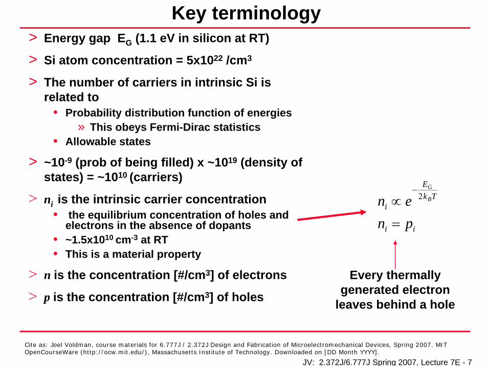
Key terminology> Energy gap EG (1.1 eV in silicon at RT)
> Si atom concentration = 5x10²² /cm3
> The number of carriers in intrinsic Si is related to
• Probability distribution function of energies» This obeys Fermi-Dirac statistics
• Allowable states
> ~10-9 (prob of being filled) x ~1019 (density of states) = ~1010 (carriers)
> ni is the intrinsic carrier concentration• the equilibrium concentration of holes and
electrons in the absence of dopants• ~1.5x1010 cm-3 at RT• This is a material property
> n is the concentration [#/cm3] of electrons
> p is the concentration [#/cm3] of holes
ii
TkE
i
pnen B
G
=∝
−2
Every thermally generated electron
leaves behind a hole

Cite as: Joel Voldman, course materials for 6.777J / 2.372J Design and Fabrication of Microelectromechanical Devices, Spring 2007. MIT OpenCourseWare (http://ocw.mit.edu/), Massachusetts Institute of Technology. Downloaded on [DD Month YYYY].
JV: 2.372J/6.777J Spring 2007, Lecture 7E - 8
Key terminology> Intrinsic carrier concentration of
Si, Ge, and GaAs1014
1013
1012
1011
1010
109
108
107
106
105200 300 400 500 600 700
T (K)In
trins
ic c
arrie
r con
cent
ratio
n (c
m-3
)
GaAs
Si
Ge
Adapted from Figure 2.20 in: Pierret, Robert F. Semiconductor Device Fundamentals.Reading, MA: Addison-Wesley, 1996, p. 54. ISBN: 9780131784598.
Image by MIT OpenCourseWare.

Cite as: Joel Voldman, course materials for 6.777J / 2.372J Design and Fabrication of Microelectromechanical Devices, Spring 2007. MIT OpenCourseWare (http://ocw.mit.edu/), Massachusetts Institute of Technology. Downloaded on [DD Month YYYY].
JV: 2.372J/6.777J Spring 2007, Lecture 7E - 9
Doped semiconductors> Dopants: substitutional impurity
atoms introduced having one different valence than the semiconductor
> Acceptor dopant concentrations arNA [#/cm3] p-type material
• Boron (3 valence electrons)
> Donor dopant concentrations are N[#/cm3] n-type material
• Phosphorous (5 valence electrons)
> These introduce new energy levels close to valence or conduction bands (~0.05 eV)
> Dopant concentrations >> ni
e
D
T=0 K
Image by MIT OpenCourseWare.7.5 in: Razeghi, M. Fundamentals of Solid
Si
Si
Si Si Si
Si
Si
Si
P
Adapted from Figure State Engineering. 2nd ed. New York, NY: Springer, 2006, p. 238.ISBN: 9780387281520.

Cite as: Joel Voldman, course materials for 6.777J / 2.372J Design and Fabrication of Microelectromechanical Devices, Spring 2007. MIT OpenCourseWare (http://ocw.mit.edu/), Massachusetts Institute of Technology. Downloaded on [DD Month YYYY].
JV: 2.372J/6.777J Spring 2007, Lecture 7E - 10
Doped semiconductors> Energy to ionize << kT (at RT)
> We assume all dopants are ionized at RT
n-type dopant
p-type dopant
Ec
Ec
EAEv
ED
Ev
T = 0 T > 0 K T = 300 K
Image by MIT OpenCourseWare.
Adapted from Figure 2.13 in: Pierret, Robert F. Semiconductor Device Fundamentals. Reading,MA: Addison-Wesley, 1996, p. 38. ISBN: 9780131784598.

Cite as: Joel Voldman, course materials for 6.777J / 2.372J Design and Fabrication of Microelectromechanical Devices, Spring 2007. MIT OpenCourseWare (http://ocw.mit.edu/), Massachusetts Institute of Technology. Downloaded on [DD Month YYYY].
JV: 2.372J/6.777J Spring 2007, Lecture 7E - 11
Main results> Donors or acceptors are fully ionized
> Define n0 and p0 as the electron and hole concentrations at equilibrium
> n0 and p0 follow a mass-action law
D D
A A
D D
A A
N N e
N N h
N N
N N
+ −
− +
+
−
→ +
→ +
≈
≈
20 0 in p n=
AN p− = DN n+ = n p=
+
-
+
-
+
-

Cite as: Joel Voldman, course materials for 6.777J / 2.372J Design and Fabrication of Microelectromechanical Devices, Spring 2007. MIT OpenCourseWare (http://ocw.mit.edu/), Massachusetts Institute of Technology. Downloaded on [DD Month YYYY].
JV: 2.372J/6.777J Spring 2007, Lecture 7E - 12
Main results> Overall, silicon is neutral
• Can use to determine n0 and p0
> Carrier concentrations typically vary over many orders of magnitude
• Can use this to simplify
> Ex:• ni ~ 1010 cm-3
• NA, ND ~ 1016-1019 cm-3
> In a given material at equilibrium• NA > 100ND (p-type)• ND > 100NA (n-type)
02 2
00
A
i i
A
p N
n nnp N
≈
= =
For p-type material:
0 0
0 0
Charge neutrality requires:
A D
A D
N n N p
N n N p
− ++ = +
+ ≈ +

Cite as: Joel Voldman, course materials for 6.777J / 2.372J Design and Fabrication of Microelectromechanical Devices, Spring 2007. MIT OpenCourseWare (http://ocw.mit.edu/), Massachusetts Institute of Technology. Downloaded on [DD Month YYYY].
JV: 2.372J/6.777J Spring 2007, Lecture 7E - 13
Main results> Therefore, the equilibrium
majority carrier concentration is determined by the net doping and the minority carrier concentration is determined by the n0p0 product.
> For typical numbers, minority carrier concentration is much less majority carrier concentration
n-type
02
0
A
i
A
p N
nnN
=
=
02
0
D
i
D
n N
npN
=
=
p-type
( )
17 3
17 30
210 323 3
0 17 3
~ 10
10
1010
10
A
A
i
A
N cm
p N cm
cmnn cmN cm
−
−
−−
−
= =
= = =

Cite as: Joel Voldman, course materials for 6.777J / 2.372J Design and Fabrication of Microelectromechanical Devices, Spring 2007. MIT OpenCourseWare (http://ocw.mit.edu/), Massachusetts Institute of Technology. Downloaded on [DD Month YYYY].
JV: 2.372J/6.777J Spring 2007, Lecture 7E - 14
Excess carriers> We can do various things to
create excess carriers• Shine light• Apply electric fields
> Excess carriers (n’, p’) represent a departure from equilibrium
> Excess holes and electrons are created in pairs
> Excess carriers recombine exponentially in pairs, governed by lifetime
• The minority carrier lifetime
0 0 Generally,
( ) ~ (0) m
mt
n n n p p pn p
dn ndt
n t n e τ
τ−
′ ′= − = −′ ′=
′ ′∝ −
′ ′
Recombination rate
Electron-hole pair (EHP)

Cite as: Joel Voldman, course materials for 6.777J / 2.372J Design and Fabrication of Microelectromechanical DOpenCourseWare (http://ocw.mit.edu/), Massachusetts Institute of Technology. Downloaded on [DD Month YYYY].
JV: 2.372J/6.777J Spring 2007, Lecture 7E - 15
Excess carriers> GaAs w/ NA=p0=1015 cm-3
> GaAs ni = 106 cm-3
> Therefore, n0= 10-3 cm-3
> Create 1014 EHP/cm3 and calculate carrier concentrations over time
0 101012
1013
1014
1015
20 30 40 50time (ns)
Car
rier c
once
ntra
tions
(cm
-3)
n(t)
p(t)
p0
Adapted from Figure 4.7 in: Streetman, Ben G., and Sanjay Kumar Banerjee.Solid State Electronic Devices. 6th ed. Upper Saddle River, NJ: PearsonPrentice Hall, 2006, p. 127. ISBN: 9780131497269.
Image by MIT OpenCourseWare.
evices, Spring 2007. MIT
Cite as: Joel Voldman, course materials for 6.777J / 2.372J Design and Fabrication of Microelectromechanical Devices, Spring 2007. MIT OpenCourseWare (http://ocw.mit.edu/), Massachusetts Institute of Technology. Downloaded on [DD Month YYYY].
JV: 2.372J/6.777J Spring 2007, Lecture 7E - 16
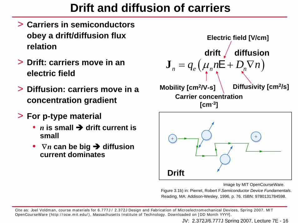
Drift and diffusion of carriers> Carriers in semiconductors
obey a drift/diffusion flux relation
> Drift: carriers move in an electric field
> Diffusion: carriers move in a concentration gradient
> For p-type material• n is small drift current is
small• ∇n can be big diffusion
current dominates
diffusiondrift( )n e n nq n D nμ= + ∇J E
Mobility [cm2/V-s]
Electric field [V/cm]
Carrier concentration [cm-3]
Diffusivity [cm2/s]
+ +
Drift
Figure 3.1b) in: Pierret, Robert F.Reading, MA: Addison-Wesley, 1996, p. 76. ISBN: 9780131784598.
Image by MIT OpenCourseWare. Semiconductor Device Fundamentals.

Cite as: Joel Voldman, course materials for 6.777J / 2.372J Design and Fabrication of Microelectromechanical Devices, Spring 2007. MIT OpenCourseWare (http://ocw.mit.edu/), Massachusetts Institute of Technology. Downloaded on [DD Month YYYY].
JV: 2.372J/6.777J Spring 2007, Lecture 7E - 17
Outline> Elements of circuit analysis
> Elements of semiconductor physics
> Semiconductor diodes and resistors
> The MOSFET and the MOSFET inverter/amplifier
> Op-amps

Cite as: Joel Voldman, course materials for 6.777J / 2.372J Design and Fabrication of Microelectromechanical Devices, Spring 2007. MIT OpenCourseWare (http://ocw.mit.edu/), Massachusetts Institute of Technology. Downloaded on [DD Month YYYY].
JV: 2.372J/6.777J Spring 2007, Lecture 7E - 18
The semiconductor diode> A p-n junction has very different
concentrations of carriers in the two regions, creating a diffusive driving force
> At equilibrium diffusive driving force = electric field in the vicinity of the junction
> In order to set up this electric field, the ionized donors and acceptors are relatively depleted of mobile carriers near the junction – the space-charge layer (SCL) or depletion region
xn0
XJ0
φxp0
--
--
--
--
--
--
--
--
--
--
--
--
--
--
--
--
--
--
--
--
--
--
--
--
--
--
--
--
--
--
--
--
--
--
--
--
--
--
--
--
--
--
--
--
--
--
--
--
++
++
++
++
++
++
++
++
++
++
++
++
++
++
++
++
++
++
++
++
++
++
++
++
++
++
++
E
p-type n-type
n-type substrate
p-type region
Oxide
Adapted from Figure 14.1 in: SenturiaBoston, MA: Kluwer Academic Publishers, 2001, p. 357. ISBN: 9780792372462.
Image by MIT OpenCourseWare., Stephen D. Microsystem Design.

Cite as: Joel Voldman, course materials for 6.777J / 2.372J Design and Fabrication of Microelectromechanical Devices, Spring 2007. MIT OpenCourseWare (http://ocw.mit.edu/), Massachusetts Institute of Technology. Downloaded on [DD Month YYYY].
JV: 2.372J/6.777J Spring 2007, Lecture 7E - 19
The exponential diode> An external voltage modifies the net
potential drop across the space charge layer
> Forward bias reduces the barrier to diffusion, leading to an increase in current
> Reverse bias increases the barrier, so only current is due to minority carriers generated in or near the space-charge layer
n-type substrate
Metalp-type region
Oxide+
_
VD
ID
Adapted from Figure 14.2 in: Senturia, Stephen D. MBoston, MA: Kluwer Academic Publishers, 2001, p. 359. ISBN: 9780792372462.
Ec
Ev
Ec
IN
IP
Ev
p
n
Equilibrium
Forward bias
Adapted from FiguDevice Fundamentals. Reading, MA: Addison-Wesley, 1996,p. 236. ISBN: 9780131784598.icrosystem Design.
Image by MIT OpenCourseWare.re 6.1 in: Pierret, Robert F. Semiconductor
Image by MIT OpenCourseWare.

Cite as: Joel Voldman, course materials for 6.777J / 2.372J Design and Fabrication of Microelectromechanical Devices, Spring 2007. MIT OpenCourseWare (http://ocw.mit.edu/), Massachusetts Institute of Technology. Downloaded on [DD Month YYYY].
JV: 2.372J/6.777J Spring 2007, Lecture 7E - 20
Ideal Exponential Diode Analysis> Linear changes in
voltage lead to exponential changes in carrier concentrations
0
The total current is
1q Ve Dk TB
DI I e⎛ ⎞
= −⎜ ⎟⎜ ⎟⎝ ⎠
Forward bias
Reverse blocking
Reverse breakdown
0.010
0.005
0.000
-0.005
-0.010-6 -5 -4 -3 -2 -1 0 1
-VB
Voltage (V)C
urre
nt (A
)
Adapted from Figure 14.3 in: Senturia, Stephen D. Microsystem Design. Boston,MA: Kluwer Academic Publishers, 2001, p. 360. ISBN: 9780792372462.
Image by MIT OpenCourseWare.

Cite as: Joel Voldman, course materials for 6.777J / 2.372J Design and Fabrication of Microelectromechanical Devices, Spring 2007. MIT OpenCourseWare (http://ocw.mit.edu/), Massachusetts Institute of Technology. Downloaded on [DD Month YYYY].
JV: 2.372J/6.777J Spring 2007, Lecture 7E - 21
The Junction-Isolated Diffused Resistor> The structure is a diode, but with two
contacts
> The diode action prevents currents into the substrate provided the diode is always reverse biased
> The conductivity is controlled by doping
> The resistor value is determined by geometry
v+-v
+-
desired undesired
n-type substrate
p-type region
Oxide Metal
distributed diode
resistor
Adapted from FigureDesign. Boston, MA: Kluwer Academic Publishers, 2001, p.363. ISBN: 9780792372462.
Image by MIT OpenCourseWare. 14.7 in: Senturia, Stephen D. Microsystem

Cite as: Joel Voldman, course materials for 6.777J / 2.372J Design and Fabrication of Microelectromechanical Devices, Spring 2007. MIT OpenCourseWare (http://ocw.mit.edu/), Massachusetts Institute of Technology. Downloaded on [DD Month YYYY].
JV: 2.372J/6.777J Spring 2007, Lecture 7E - 22
Outline> Elements of circuit analysis
> Elements of semiconductor physics
> Semiconductor diodes and resistors
> The MOSFET and the MOSFET inverter/amplifier
> Op-amps

Cite as: Joel Voldman, course materials for 6.777J / 2.372J Design and Fabrication of Microelectromechanical Devices, Spring 2007. MIT OpenCourseWare (http://ocw.mit.edu/), Massachusetts Institute of Technology. Downloaded on [DD Month YYYY].
JV: 2.372J/6.777J Spring 2007, Lecture 7E - 23
MOSFET Structure
> The MOSFET exploits the concept of a field-induced junction
> The electric field between the gate and the channel region of the substrate can either increase the surface concentration (accumulation) or deplete the surface and eventually invert the surface
p-type substrate
Oxide
Source Gate Drain
G
S
B
D
Body
n+ regionsChannels
Adapted from Figure 14.10 in: Senturia, Stephen D. Microsystem Design.Boston, MA: Kluwer Academic Publishers, 2001, p. 366. ISBN: 9780792372462.
Image by MIT OpenCourseWare.

Cite as: Joel Voldman, course materials for 6.777J / 2.372J Design and Fabrication of Microelectromechanical Devices, Spring 2007. MIT OpenCourseWare (http://ocw.mit.edu/), Massachusetts Institute of Technology. Downloaded on [DD Month YYYY].
JV: 2.372J/6.777J Spring 2007, Lecture 7E - 24
MOSFET qualitative operation
> With D & S grounded, back-to-back diodes prevent current flow between D & S
> To reduce barrier, apply positive voltage to G (w.r.t. D & S)
> At some threshold voltage, this will form an n-channel inversion layer that will connect D & S

Cite as: Joel Voldman, course materials for 6.777J / 2.372J Design and Fabrication of Microelectromechanical Devices, Spring 2007. MIT OpenCourseWare (http://ocw.mit.edu/), Massachusetts Institute of Technology. Downloaded on [DD Month YYYY].
JV: 2.372J/6.777J Spring 2007, Lecture 7E - 25
MOSFET Characteristics> Need VGS>VT for device to turn on
> As VDS increases, current will flow between D & S
> As VDS increases, voltage between G and D decreases
> When VDS gets too big, one side of channel pinches off, preventing further increases in current
S G GSD
e-e-
SD
e-e-
V VDS GS T> -VVDS>0
GD
e-e-
n-channel
VDS=0
1000
800
600
400
200
00 1 2 3 4 5
VGS = 3 V
VDS
ID,sat
VGS = 2 V
triode
saturation
I D (µ
A)
VGS = 4 V
Adapted from Figure 14.13 in: Senturia, Stephen D. Microsystem Design.Boston, MA: Kluwer Academic Publishers, 2001, p. 369. ISBN: 9780792372462.
Image by MIT OpenCourseWare.
Cite as: Joel Voldman, course materials for 6.777J / 2.372J Design and Fabrication of Microelectromechanical Devices, Spring 2007. MIT OpenCourseWare (http://ocw.mit.edu/), Massachusetts Institute of Technology. Downloaded on [DD Month YYYY].
JV: 2.372J/6.777J Spring 2007, Lecture 7E - 26
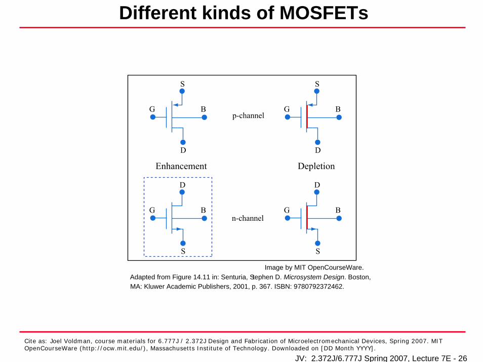
Different kinds of MOSFETs
G
D
B
S
G
D
B
S
G
S
B
D
G
S
B
D
p-channel
n-channel
Enhancement Depletion
Adapted from Figure 14.11 in: Senturia, SMA: Kluwer Academic Publishers, 2001, p. 367. ISBN: 9780792372462.
Image by MIT OpenCourseWare.tephen D. Microsystem Design. Boston,

Cite as: Joel Voldman, course materials for 6.777J / 2.372J Design and Fabrication of Microelectromechanical Devices, Spring 2007. MIT OpenCourseWare (http://ocw.mit.edu/), Massachusetts Institute of Technology. Downloaded on [DD Month YYYY].
JV: 2.372J/6.777J Spring 2007, Lecture 7E - 27
Large-signal and small-signal MOSFET models> Electrical engineers use
circuit models to analyze circuits involving MOSFETS
> Can use either full nonlinear characteristics
> Or linearized small-signal model
• Different models include different components
Simple large-signal model, in saturation
Simple small-signal model, in saturation
G
D
S
K/2(V -V )GS Tn2
G
D
S
+-
g vm gsCGSr0

Cite as: Joel Voldman, course materials for 6.777J / 2.372J Design and Fabrication of Microelectromechanical Devices, Spring 2007. MIT OpenCourseWare (http://ocw.mit.edu/), Massachusetts Institute of Technology. Downloaded on [DD Month YYYY].
JV: 2.372J/6.777J Spring 2007, Lecture 7E - 28
Outline> Elements of circuit analysis
> Elements of semiconductor physics• Semiconductor diodes and resistors• The MOSFET and the MOSFET inverter/amplifier
> Op-amps

Cite as: Joel Voldman, course materials for 6.777J / 2.372J Design and Fabrication of Microelectromechanical Devices, Spring 2007. MIT OpenCourseWare (http://ocw.mit.edu/), Massachusetts Institute of Technology. Downloaded on [DD Month YYYY].
JV: 2.372J/6.777J Spring 2007, Lecture 7E - 29
Operational Amplifiers – op-amps> Let someone else design a high-performance amplifier> Basic structure and transfer characteristic
LM158
_
+
v-
VS+
VS-
v+
v+v-
v0
v0
v0
v+ - v-
Vsat-
Vsat+
v+
Differentialamplifier
High-gainamplifier
Output amplifier
Signal path
Output A
Inverting input A
Non-inverting input A
Non-inverting Input B
Output B
Inverting input B
1
2
3
4 5
6
7
8
GND
DIP/SO Package
Slope A0
A B_ _+ +
Top view
_
+
Adapted from Figures 14.23 and 14.24 in Senturia, Stephen D. Microsystem Design. Boston, MA: Kluwer Academic Publishers,2001, p. 382. ISBN: 9780792372462.
Image by MIT OpenCourseWare.

Cite as: Joel Voldman, course materials for 6.777J / 2.372J Design and Fabrication of Microelectromechanical Devices, Spring 2007. MIT OpenCourseWare (http://ocw.mit.edu/), Massachusetts Institute of Technology. Downloaded on [DD Month YYYY].
JV: 2.372J/6.777J Spring 2007, Lecture 7E - 30
Ideal and non-ideal behavior> We do first analysis using ideal
linear model
> Op-amp data sheets have pages and pages of limitations
> A sampling• Input offset voltage voff: zero
volts at input gives non-zero output
• Frequency limitations: op-amps can only amplify up to a maximum frequency
( )0
0 0
0
( ) ( ) ( ) ( )where
( )
v s A s v s v s
A sA ss s
+ −= −
=+

Cite as: Joel Voldman, course materials for 6.777J / 2.372J Design and Fabrication of Microelectromechanical Devices, Spring 2007. MIT OpenCourseWare (http://ocw.mit.edu/), Massachusetts Institute of Technology. Downloaded on [DD Month YYYY].
JV: 2.372J/6.777J Spring 2007, Lecture 7E - 31
The Inverting Amplifier
0
1 2
0
2
1 2
1
2
1
KCL:
(0 )
111 1
s
o
s
o
s
V v v VR R
V A v
V RV R R
A R
AV RV R
− −
−
− −=
⇓ = −
⇓
⎡ ⎤⎢ ⎥⎢ ⎥= −⎢ ⎥⎛ ⎞+ +⎢ ⎥⎜ ⎟
⎢ ⎥⎝ ⎠⎣ ⎦⇓ →∞
= −
Assume op-amp draws no current
Use Nodal analysis:
Vs Vo+-
+-
A(v -v )+ -
v-
v+
R1
R2
Vs Vo+-
v-
v+
R1
R2
+
-

Cite as: Joel Voldman, course materials for 6.777J / 2.372J Design and Fabrication of Microelectromechanical Devices, Spring 2007. MIT OpenCourseWare (http://ocw.mit.edu/), Massachusetts Institute of Technology. Downloaded on [DD Month YYYY].
JV: 2.372J/6.777J Spring 2007, Lecture 7E - 32
Short method for analyzing op-amps> Assume linear region operation
• This implies that the two inputs are essentially at the same voltage (but never exactly equal)
> Assume zero currents at both inputs
> Analyze the external circuit with these constraints
> Check to verify that the output is not at either saturation limit (±VS)

Cite as: Joel Voldman, course materials for 6.777J / 2.372J Design and Fabrication of Microelectromechanical Devices, Spring 2007. MIT OpenCourseWare (http://ocw.mit.edu/), Massachusetts Institute of Technology. Downloaded on [DD Month YYYY].
JV: 2.372J/6.777J Spring 2007, Lecture 7E - 33
More op-amp configurations
20
2 1
0 1
2
1
S
s
S
v v VRV V
R RV RV R
− += =
=+
= +
V0
Vs
R1
R2
Non-inverting
+
_
Adapted from Figure 14.28 in Senturia, Stephen D. Microsystem Design.Boston, MA: Kluwer Academic Publishers, 2001, p. 388. ISBN: 9780792372462.
Image by MIT OpenCourseWare.

Cite as: Joel Voldman, course materials for 6.777J / 2.372J Design and Fabrication of Microelectromechanical Devices, Spring 2007. MIT OpenCourseWare (http://ocw.mit.edu/), Massachusetts Institute of Technology. Downloaded on [DD Month YYYY].
JV: 2.372J/6.777J Spring 2007, Lecture 7E - 34
More op-amp configurations
Transimpedance amplifier
SIRV 10 −=
+
_
Is
R1
V0
Adapted from Figure 14.29 in Senturia, Stephen D. Microsystem Design. Boston, MA: Kluwer Academic Publishers, 2001, p. 389. ISBN: 9780792372462.
Image by MIT OpenCourseWare.

Cite as: Joel Voldman, course materials for 6.777J / 2.372J Design and Fabrication of Microelectromechanical Devices, Spring 2007. MIT OpenCourseWare (http://ocw.mit.edu/), Massachusetts Institute of Technology. Downloaded on [DD Month YYYY].
JV: 2.372J/6.777J Spring 2007, Lecture 7E - 35
Integrator
dttVCR
V s )(1
10 ∫−=
Vs V0
C
R1 +
+
+
_
_
_vC
Adapted from Figure 14.30 in Senturia, Stephen D. Microsystem Design. Boston,MA: Kluwer Academic Publishers, 2001, p. 389. ISBN: 9780792372462.
Image by MIT OpenCourseWare.

Cite as: Joel Voldman, course materials for 6.777J / 2.372J Design and Fabrication of Microelectromechanical Devices, Spring 2007. MIT OpenCourseWare (http://ocw.mit.edu/), Massachusetts Institute of Technology. Downloaded on [DD Month YYYY].
JV: 2.372J/6.777J Spring 2007, Lecture 7E - 36
Differentiator
0
1
01
The differentiator is less "ideal"
01
s
s
V VRsC
V sR CV
−=
= −
Vs V0
C
R1
+
+
_
_
Adapted from Figure 14.31 in Senturia, Stephen D. Microsystem Design. Boston,MA: Kluwer Academic Publishers, 2001, p. 390. ISBN: 9780792372462.
Image by MIT OpenCourseWare.