elen 624 signal integrity - · pdf fileelen 624 signal integrity jin zhao ... high speed...
TRANSCRIPT

ELEN 624 Signal Integrity
Department of Electrical EngineeringSanta Clara University
ELEN 624, Fall 2005 Week 01, 09/26/2005

Contents
• Introduction• Course outline and tentative lecture schedule• Some useful information
• Basic circuit component (R, C, L, M) properties review• Basic RC, RL, and RLC circuit analysis• SPICE circuit simulation• Homework
ELEN 624, Fall 2005 Week 01, 09/26/2005, Page 2

Introduction, Course Outline, Tentative Schedule
Top Signal LayerGND Plane LayerInner Signal Layer1
Inner Signal Layer2PWR Plane LayerBottom Signal Layer
PCB
Package
Chip/Die
P/G supplySignalC4 layer
Solder Ball layer
Decaps
OtherPackages and Chips Connector
Daughter Cards
System Power Supply
A system
Signal transmission system, deliver the signalPower delivery system, to make sure the device will work properlySignal transmission system, deliver the signal
Power delivery system, to make sure the device will work properlySignal transmission system, deliver the signalPower delivery system, to make sure the device will work properly
Interaction/coupling within the system, between two systems
ELEN 624, Fall 2005 Week 01, 09/26/2005, Page 3

Signal Integrity, Power Integrity
A system contains modeling, simulation, analysis and design
Modeling use EM field solver to generate engineering acceptable (circuit) model
Simulation use EM simulator or circuit simulator (SPICE) to perform simulation based on the model
Analysis interpret the simulation results, make design recommendations ordesign guidelines, rules, etc.
Design Based on analysis results, follow the guideline, to control the signal propagation properties, to meet the specification
Optimization Balance the cost the system performance
ELEN 624, Fall 2005 Week 01, 09/26/2005, Page 4

Course Objective
An introduction course
Introduce signal and power integrity fundamental principles and practice in the analysis and design of high-speed IC circuits, IC package and PCBs.
The ability of judging the simulation results
The skills of using various simulation software
ELEN 624, Fall 2005 Week 01, 09/26/2005, Page 5

Course Description
Lay the foundation of signal and power integrity
To cover various fundamental signal and power integrity issues involved in IC, package and printed circuit board environments.
Started with basic circuitsTransmission line analysisVarious interconnectionsPower integrity issuesSystem level channel simulationsSystem level timing considerationsEMI/EMC
Simulation skills
Results interpretation
ELEN 624, Fall 2005 Week 01, 09/26/2005, Page 6

Course Schedule
ELEN 624, Fall 2005 Week 01, 09/26/2005, Page 7

Course Schedule
ELEN 624, Fall 2005 Week 01, 09/26/2005, Page 8

Some Useful Information
Simulation Tools:HSPICE, Ansoft, Fastcap, Fasthenry (www.fastfieldsolvers.com)PSPICE (www.pspice.com), Berkeley SPICEwww.engr.scu.edu/mourad/cadtools.html
Reference books:• Howard Johnson and Martin Graham, High Speed Digital Design and High Speed
Signal Propagation: Advanced Black Magic• By Dally and Poulton, Digital System Engineering• Brian Young, Digital Signal Integrity• Ramo, Whinnery, Van Duzer, Field and Waves in Communication Electronics• David M. Pozar, Microwave Engineering
Si-List
ELEN 624, Fall 2005 Week 01, 09/26/2005, Page 9
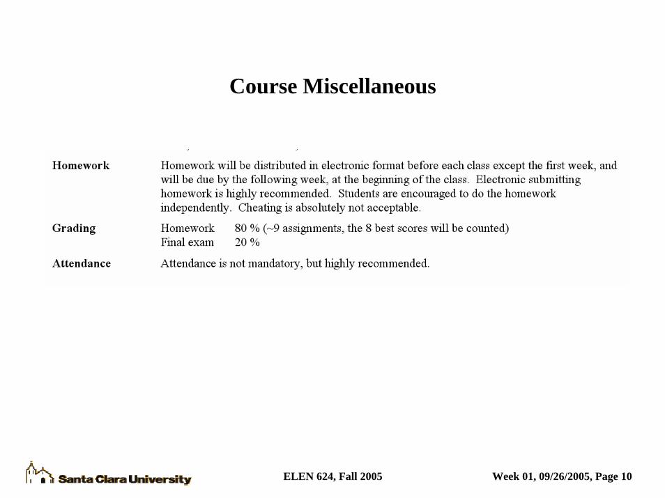
Course Miscellaneous
ELEN 624, Fall 2005 Week 01, 09/26/2005, Page 10

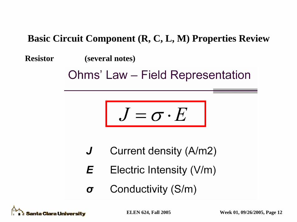
Basic Circuit Component (R, C, L, M) Properties Review
Resistor
Ohms law V = IR
Power loss = I2R = V2/R+ V -
I
Energy loss = RdttidttpTT
)()( 2∫=∫∞−∞− i
Slope =1/R
v
ELEN 624, Fall 2005 Week 01, 09/26/2005, Page 11
Basic Circuit Component (R, C, L, M) Properties Review
Resistor (several notes)
ELEN 624, Fall 2005 Week 01, 09/26/2005, Page 12

Basic Circuit Component (R, C, L, M) Properties Review
Resistor (several notes)
ELEN 624, Fall 2005 Week 01, 09/26/2005, Page 13

Basic Circuit Component (R, C, L, M) Properties Review
Resistor (several notes)
ELEN 624, Fall 2005 Week 01, 09/26/2005, Page 14

Basic Circuit Component (R, C, L, M) Properties Review
Capacitor
+ V -
I
∫+=
=
tdi
Cvtv
dtdvCti
0;)(1)0()(
;)(
ττQ Slope =C
vQ=CV; i(t) = dq/dt
2
21)()()()( CVdttv
dtdvCdttvtidttp
TTT=∫=∫=∫
∞−∞−∞−Energy =
ELEN 624, Fall 2005 Week 01, 09/26/2005, Page 15

Basic Circuit Component (R, C, L, M) Properties Review
Capacitor (several notes)
ELEN 624, Fall 2005 Week 01, 09/26/2005, Page 16

Basic Circuit Component (R, C, L, M) Properties Review
Capacitor (several notes)
ELEN 624, Fall 2005 Week 01, 09/26/2005, Page 17

Basic Circuit Component (R, C, L, M) Properties Review
Capacitor (several notes)
ELEN 624, Fall 2005 Week 01, 09/26/2005, Page 18
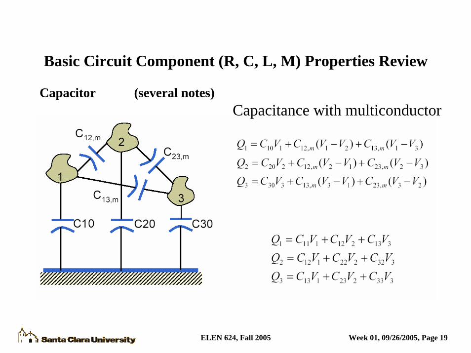
Basic Circuit Component (R, C, L, M) Properties Review
Capacitor (several notes)Capacitance with multiconductor
ELEN 624, Fall 2005 Week 01, 09/26/2005, Page 19

Basic Circuit Component (R, C, L, M) Properties Review
Capacitor (several notes)
ELEN 624, Fall 2005 Week 01, 09/26/2005, Page 20

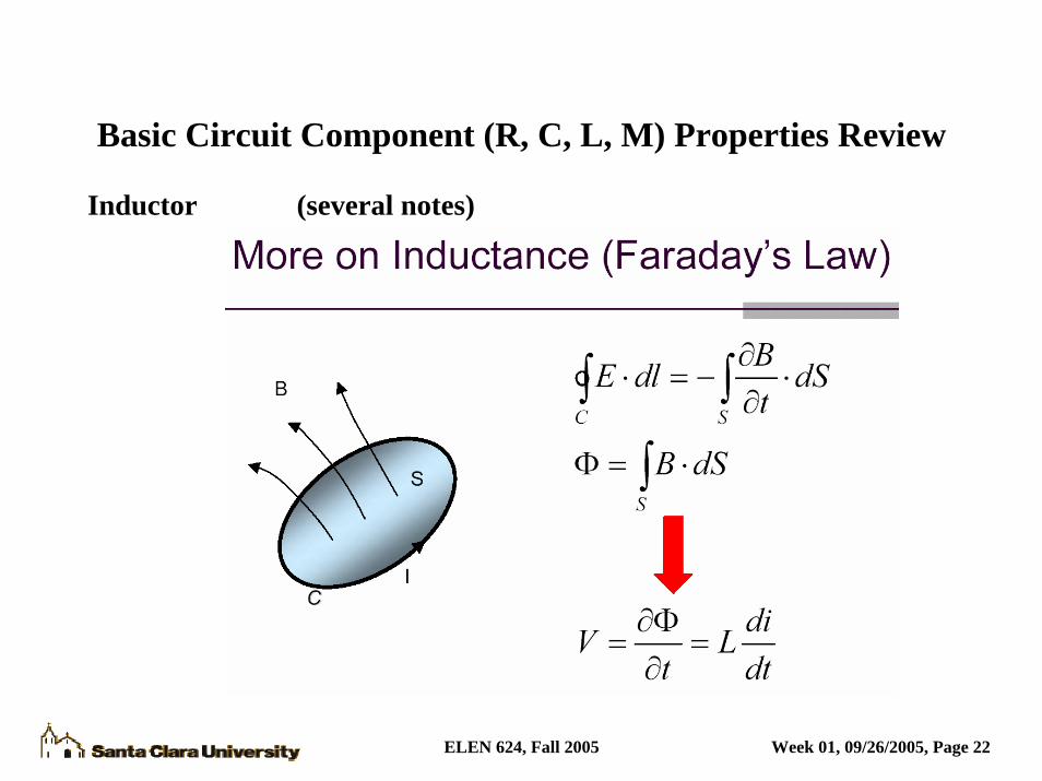
Basic Circuit Component (R, C, L, M) Properties Review
Inductor
+ V -
I
∫+=
=
tdv
Liti
dtdiLtv
0;)(1)0()(
;)(
ττ
Lλ Slope =L
iψ=LI; v(t) = dψ/dt
2
21)()()()( LIdt
dtdiLtidttvtidttp
TTT=∫=∫=∫
∞−∞−∞−Energy =
ELEN 624, Fall 2005 Week 01, 09/26/2005, Page 21
Basic Circuit Component (R, C, L, M) Properties Review
Inductor (several notes)
ELEN 624, Fall 2005 Week 01, 09/26/2005, Page 22

Basic Circuit Component (R, C, L, M) Properties Review
Inductor (several notes)
ELEN 624, Fall 2005 Week 01, 09/26/2005, Page 23

Basic Circuit Component (R, C, L, M) Properties Review
Mutual Inductor
Loop1 Loop2
21
21121
122 ;
LLMK
MMMdtdiMV
=
===
K can be positive or negative
K negativeK positive
ELEN 624, Fall 2005 Week 01, 09/26/2005, Page 24
Basic Circuit Component (R, C, L, M) Properties Review
Inductor (several notes)
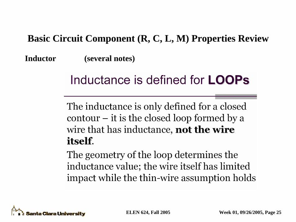
ELEN 624, Fall 2005 Week 01, 09/26/2005, Page 25

Basic Circuit Component (R, C, L, M) Properties Review
Inductor (several notes)
ELEN 624, Fall 2005 Week 01, 09/26/2005, Page 26
Basic Circuit Component (R, C, L, M) Properties Review
Inductor (several notes)
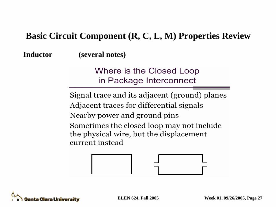
ELEN 624, Fall 2005 Week 01, 09/26/2005, Page 27

Basic Circuit Component (R, C, L, M) Properties Review
Inductor (several notes)
ELEN 624, Fall 2005 Week 01, 09/26/2005, Page 28

Basic Circuit Component (R, C, L, M) Properties Review
Inductor (several notes)
ELEN 624, Fall 2005 Week 01, 09/26/2005, Page 29
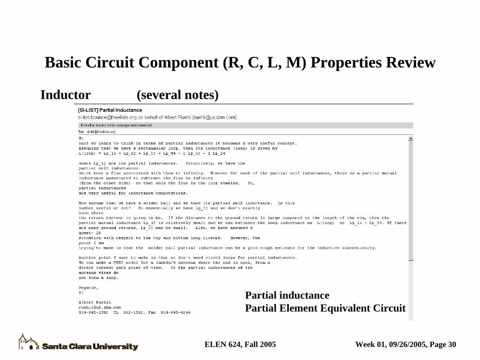
Basic Circuit Component (R, C, L, M) Properties Review
Inductor (several notes)
Partial inductancePartial Element Equivalent Circuit
ELEN 624, Fall 2005 Week 01, 09/26/2005, Page 30
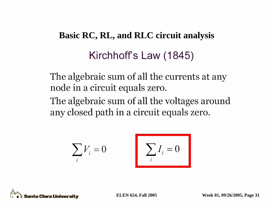
Basic RC, RL, and RLC circuit analysis
ELEN 624, Fall 2005 Week 01, 09/26/2005, Page 31

Basic RC, RL, and RLC circuit analysis
+ +- -
R
c
V0
C V
t=0
0
)1()(
0
0
0
0
RCt
c
cc
cc
eVtv
RCV
RCv
dtdv
dtdvC
RVv
−
−=
=+
=+−
V0
vc(t)
ELEN 624, Fall 2005 Week 01, 09/26/2005, Page 32
t
t=RC
vc(t) = 0.63V0
Kirchoff’s current lawused; algebraic sum ofcurrents at node = 0

Basic RC, RL, and RLC circuit analysis
ELEN 624, Fall 2005 Week 01, 09/26/2005, Page 33

Basic RC, RL, and RLC circuit analysis
+ +- -
R
vL
t=0
0
V0
RLt
L
LL
t
LL
eVtv
LRv
dtdv
dvLR
Vv
/0
0
0
)(
0
0)(1
−
=
=+
=∫+− ττ
ELEN 624, Fall 2005 Week 01, 09/26/2005, Page 34
t
t=RC
vL(t) = 0.37V0
V0
vL(t)

Basic RC, RL, and RLC circuit analysis
+
-
R
t=0
0
+ -vLV0
0
1
2
2
0
=++
=∫++
LCi
dtdi
LR
dtid
VidtCdt
diLRi + vci(t)
-
tt BeAeti 21)( αα +=where
Solution of the form
Kirchoff’s voltage lawused; algebraic sum ofvoltages around mesh = 0 LCL
RL
R 122
,2
21 −⎟⎠⎞
⎜⎝⎛±−=αα
ELEN 624, Fall 2005 Week 01, 09/26/2005, Page 35

Basic RC, RL, and RLC circuit analysis
tt BeAeti 21)( αα +=where LCL
RL
R 122
,2
21 −⎟⎠⎞
⎜⎝⎛±−=αα
012
012
012
2
2
2
<−⎟⎠⎞
⎜⎝⎛
>−⎟⎠⎞
⎜⎝⎛
=−⎟⎠⎞
⎜⎝⎛
LCLR
LCLR
LCLR
( ) teBAti α+=)( Critical damped
Over dampedTwo real roots
tt BeAeti 21)( αα +=
Under dampedTwo complex roots
tt BeAeti 21)( αα +=
ELEN 624, Fall 2005 Week 01, 09/26/2005, Page 36

Basic RC, RL, and RLC circuit analysis
Solution of the form Initial ConditionsAt t=0, i=0At t=0, Ldi/dt=V0
2
2
21
),sincos()(
⎟⎠⎞
⎜⎝⎛−=
+=−
LR
LC
wheretBtAeti LR
ω
ωω
⎥⎥⎥
⎦
⎤
⎢⎢⎢
⎣
⎡−−=
−−=
=
−−
−
tetLReV
iRdtdiLVtv
tVL
eti
LRL
R
c
LR
ωωω
ωω
cossin2
1
)(
sin)(
22
0
0
0
2
V0
vc(t)
ELEN 624, Fall 2005 Week 01, 09/26/2005, Page 37
t

Basic RC, RL, and RLC circuit analysis
An application
+
-
R
t=0
0
+ -vLV0
Chip
VRM + vci(t)
-
LCLR
LR 1
22,
2
21 −⎟⎠⎞
⎜⎝⎛±−=αα
2
2
21
),sincos()(
⎟⎠⎞
⎜⎝⎛−=
+=−
LR
LC
wheretBtAeti LR
ω
ωω
ELEN 624, Fall 2005 Week 01, 09/26/2005, Page 38

SPICE Circuit Simulation
Time
0s 5ns 10ns 15ns 20ns 25ns 30ns 35ns 40nsV(C1:2) V(V1:+)
0V
0.2V
0.4V
0.6V
0.8V
1.0V
1.2V
V1 1 0 pulse (0 1 0 1n 1n 1 1 )R1 1 2 1L1 2 3 1nC1 3 0 1n
ELEN 624, Fall 2005 Week 01, 09/26/2005, Page 39

Homework
1. Try to recall or flash your memory on the step response of RC, RL and RLC circuit, you may find you old text book, or google that on the internet. (You don’t need to hand in anything, but it is highly recommend you do this ☺ )
2. Prepare a SPICE simulator for yourself, if you already have SPICE simulator available, you may skip this ☺
3. Use SPICE to perform circuit simulation on the circuit showing in previous slide with following parameters:R L C1 Ohm 1 nH 1 nF
Try to make three cases showing the over, critically and under –damped.Also try to make the connection between the waveforms and the RLC values, such as by using the equation on page 35.
Please plot the results together
For the Step function, also, there are two cases, rising time can be 10 ps, 1ns.
Please comment on the simulation results based on:1) Signal spectrum, you may want to plot the spectrum of the two step functions2) Components value, which means the simulation model might be simplified, such as ignore the inductor
Which is only the RC circuit, and also compare the results with the RLC circuit.
ELEN 624, Fall 2005 Week 01, 09/26/2005, Page 40