elliptic switch capacitor design - university of michigansawad/videos/ece512... · elliptic switch...
TRANSCRIPT

Elliptic Switch Capacitor Design
Dr. Selim Awad
John Drazek William Frigon Larry George
ECE 512 Filter Design
Winter 2005
DEPARTMENT OF ELECTRICAL AND COMPUTER ENGINEERING
THE UNIVERSITY OF MICHIGAN – DEARBORN
Evergreen Rd, Dearborn MI 48128-1491
Tel: (313) 593-5420 Fax: (313) 593-9967

2
Table of Contents
Introduction......................................................................................................................... 3 Elliptic Filter Background................................................................................................... 4 Switched Capacitor Background......................................................................................... 5 GIC Circuit.......................................................................................................................... 6 Design Process .................................................................................................................... 7 Filter Design Specifications................................................................................................ 8
Low Pass Notch Filter..................................................................................................... 8 Specification ............................................................................................................... 8
High Pass Notch Filter .................................................................................................... 8 Specification ............................................................................................................... 8
Band Pass Filter .............................................................................................................. 8 Specification ............................................................................................................... 8
PSPICE Simulations ........................................................................................................... 9 Low Pass Notch Filter..................................................................................................... 9
Magnitude Response................................................................................................... 9 Phase Response......................................................................................................... 11
High Pass Notch Filter .................................................................................................. 12 Magnitude Response................................................................................................. 12 Phase Response......................................................................................................... 13
Band-Pass Notch Filter ................................................................................................. 15 Magnitude Response................................................................................................. 15 Phase Response......................................................................................................... 17
Hardware Design .............................................................................................................. 18 MF10 Operation............................................................................................................ 18
Conclusion ........................................................................................................................ 26 Appendix I: Matlab Code.................................................................................................. 33
a) Low-Pass Design ...................................................................................................... 33 b) High-Pass Design ..................................................................................................... 34 c) Band-Pass Design ..................................................................................................... 35
Appendix II: Calculations for the PSPICE Design ........................................................... 37 a) Low-Pass Notch Design............................................................................................ 37 b) High-Pass Notch Design........................................................................................... 40 c) Band-Pass Design ..................................................................................................... 43
Appendix III: PSPICE Design .......................................................................................... 46 a) Low-Pass Notch Design............................................................................................ 46 b) High-Pass Notch Design........................................................................................... 48 c) Band-Pass Design ..................................................................................................... 50
Appendix IV: Calculations for the MF10 ......................................................................... 52 a) Low-Pass Design ...................................................................................................... 52 b) High-Pass Design ..................................................................................................... 54 c) Band-Pass Design ..................................................................................................... 55
Appendix V: MF10 Specification..................................................................................... 57

3
Introduction
Filters are used in a variety of applications, and throughout many different industries.
The requirements are determined by both, application and the industry that is using the
part.
For instance, in automotive applications, parts within the vehicle are subjected to varying
temperatures all day long, whether the vehicle is cruising on a mountain highway in
Colorado or strolling up and down the Vegas strip in 110oF temperatures.
Many parts are also subjected to extreme heat in the engine compartment of the
automobile as well. For this reason, Automotive OEM’s are very strict on qualify parts
and obtaining the worst-case analysis on parts for these scenarios.
For these applications, temperature changes are clearly a factor on the design. Resistors
are highly susceptible to temperature changes. The Switched Capacitor circuit takes all
of the resistors that were in the circuit, and replaces them with a capacitor and switch
combination.

4
Elliptic Filter Background Elliptic (Cauer) filters have a much narrower transition from the pass to stop band, or
vice versa. The price to pay for this feature is that Elliptic filters have equal ripple in
both the pass-band and the stop-band, due to the fact that they have both poles and
zeroes. The zeroes are imaginary.
Another benefit of choosing an Elliptic Filter design is that the order is typically 0.25 to
0.5 less than that of the order determined through a Chebychev or Butterworth design.
While designing Chebychev filters, one must use tables to determine the normalized
frequencies and quality factors. With Elliptic design, one must use a type of
mathematical calculation to determine the normalized frequencies and quality factors.
For this reason, Elliptic isn’t a favorite approach for Engineers to use.
It is important to note that it is becoming a must. As tolerances get smaller and smaller,
the need to have a fast switching (pass-band to stop-band transition) filter is becoming
greater and greater. There are also many routines that are becoming available to evaluate
and design Elliptic filters to meet ones needs.

5
Switched Capacitor Background
Resistors tend to be very heat-sensitive, meaning the resistivity changes over
temperature. Although, capacitors’ characteristics change slightly over temperature as
well, they do not change nearly as much as that of a resistor.
Also, resistors are almost impossible to implement within IC’s, while maintaining a small
size. Capacitors and switches have been implemented on IC’s for over 20 years now. It
is incredible how small the IC’s have become over the year.
Based on the requirements of a small chip size, and a low tolerance to heat, Switched
Capacitor filters are in high demand. Automotive suppliers all over the world almost
exclusively use Switch Capacitor filters.
More and more electronics are added to an automobile every year. And besides the SUV
growth in popularity, it seems vehicles are continuing to become smaller and smaller.
With more components, and less space, board size requirements are becoming
ridiculously small. Instead of having a board population of 15 resistor/capacitor/op-amp
combinations, all that is needed is one small IC, with a couple of resistors determining
the mode of operation.

6
GIC Circuit
The GIC circuit is used to implement a high-pass, low-pass, band-pass, all-pass, notch,
high-pass notch, and low-pass notch. The variables are determined, and will determine
the component values. An example of how these variables effect the transfer function is
shown in Figure 1.
Figure 1: GIC Circuit
Generic Transfer Functionα 2a c−:= c
β 2b c−:= 2b
Hs
α s2 β
α
ω0Q
s
+ c
ω02
α⋅+
s2 ω0Q
s( )+ ω02
+
≡
c
*Hc 2b:= 2b

7
Design Process
The specifications were first inputted into Matlab. They consisted of the attenuation
requirements and the cutoff frequency requirements.
Matlab determined the normalized frequencies, and gave us the normalized transfer
function of the circuit.
MathCad was used to denormalize the circuit. It also determined our quality factors.
Once denormalized, the designed parameters could be obtained. Since a GIC circuit was
used, calculating the factors a, b, and c was necessary. Once these values were obtained,
the component values were calculated.
PSPICE was used to simulate our design. We were able to see the magnitude and phase
response, and verify that the filter was designed correctly. We were also able to put
standard values in place of the “designed” values to determine what effect that had on our
circuit operation.

8
Filter Design Specifications
Low Pass Notch Filter
Specification
Our specifications for the Low Pass Notch filter consisted of a pass-band frequency of
200Hz. The stop-band frequency was chosen to be 225Hz. The attenuation in the pass-
band cannot fall beneath 2dB. The attenuation in the stop-band cannot rise about 17dB.
High Pass Notch Filter
Specification
Our specifications for the Low Pass Notch filter consisted of a pass-band frequency of
200Hz. The stop-band frequency was chosen to be 225Hz. The attenuation in the pass-
band cannot fall beneath 2dB. The attenuation in the stop-band cannot rise about 17dB.
Band Pass Filter
Specification
Our specifications for the Low Pass Notch filter consisted of a pass-band frequency of
200Hz through 7kHz. The stop-band frequency was chosen to be 225Hz and 7.5kHz.
The attenuation in the pass-band cannot fall beneath 2dB. The attenuation in the stop-
band cannot rise about 17dB.

9
PSPICE Simulations
Low Pass Notch Filter
The low pass filter magnitude response is shown in Figure 2. As shown in the plot, the actual simulated value of the cutoff frequency is within 0.1% of the specified value. Figure 3 shows the magnitude response using standard values for the components. Also noted is that the cutoff frequency is within 0.1% for this design as well. Figure 4 and Figure 5 show the phase responses for both cases.
Magnitude Response
Figure 2: Magnitude Response of LP Notch Filter using ideal values

10
Figure 3: Magnitude Response of LP Notch Filter using standard values

11
Phase Response
Figure 4: Phase Response of LP Notch Filter using ideal values
Figure 5: Phase Response of LP Notch Filter using standard values

12
High Pass Notch Filter
Figure 6 and Figure 7 show the magnitude response of the HP Notch filters. As with the LP notch design, the values of the cutoff frequencies are very close to the specified design, although not as close as in the case of the LP Notch design. The phase responses are shown in Figure 8 and Figure 9.
Magnitude Response
Figure 6: Magnitude Response of HP Notch Filter using ideal values

13
Figure 7: Magnitude Response of HP Notch Filter using ideal values
Phase Response
Figure 8: Phase Response of HP Notch Filter using ideal values

14
Figure 9: Phase Response of HP Notch Filter using standard values

15
Band-Pass Notch Filter
Figure 10 and Figure 11 show the magnitude response of the BP Notch filters. As with
the LP & HP notch design, the values of the cutoff frequencies are very close to the
specified design, although not as close as in the case of the LP Notch design. The phase
responses are shown in Figure 12 and Figure 13.
Magnitude Response
Figure 10: Magnitude Response of Band-Pass Filter using ideal values
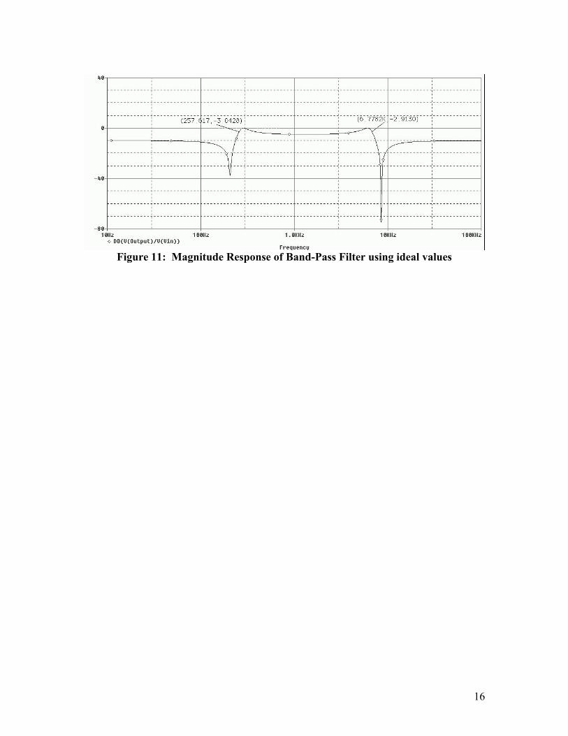
16
Figure 11: Magnitude Response of Band-Pass Filter using ideal values

17
Phase Response
Figure 12: Phase Response of Band-Pass Filter using ideal values
Figure 13: Phase Response of Band-Pass Filter using standard values

18
Hardware Design
MF10 Operation
The switched capacitor IC chip that was used is the MF10 by National
Semiconductor. The MF10 is a universal monolithic dual switched capacitor filter. It has
two independent, 2nd order CMOS active filter building blocks. With the use of an
external clock and three to four external resistors, this IC can be configured to perform a
Low-Pass, High-Pass, Band-Pass, notch, or allpass filter. A 4th order filter can be
obtained by cascading two of the 2nd order filter building blocks. A Butterworth,
Chebyshev, Elliptic, and a Bessel-Thomson filter configuration can be achieved with this
IC.
There are six different modes of operation from this IC that can realize the
different types of filters. For example, the High-Pass filter can be realized only from
modes 3, 3a, and 6a. In the MF10 datasheet, these modes are described along with
needed equations to calculate the external resistor values. There are also schematics that
are provided for each of the modes to show the user how to wire the IC.

19
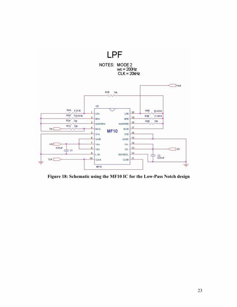
For the Low-Pass filter that was built, this the equation section for Mode 2 which was
used in Figure 14:
Figure 14: Equations used to design MF10 Implementation for the LP Notch Filter

20
This is the schematic that is provided by National Instruments for the Low-Pass filter,
Mode 2 in Figure 15:
Figure 15: Internal Schematic of the MF10 IC for the Low Pass Notch Filter

21
For the High-Pass and the Band-Pass filters, Mode 3 was chosen. Here are the equations
for Mode3 in Figure 16:
Figure 16: Equations used to design MF10 Implementation for the HP Notch Filter
and Band-Pass Filter

22
This is the schematic that is provided by National Instruments for the high-pass and band-
pass filters, Mode 3 in Figure 17:
Figure 17: Internal Schematic of the MF10 IC for the High-Pass Notch and Band-
Pass Filters
The IC can be configured to operate on a single power supply (+10V) or a dual
supply (+/- 5V). The +/- 5V-supply configuration was used. The datasheet also provides
some examples for a Low-Pass filter. This example was followed for the lowapss filter
that was built and was successful. The High-Pass and the Band-Pass filters were also
modeled after the example, however, neither of these filters was realizable.
The calculations of how the MF10 parts were configured for each type of filter
can be found in the appendix, while the actual schematics for each design are shown in
Figure 18, Figure 19, and Figure 20.
23
Figure 18: Schematic using the MF10 IC for the Low-Pass Notch design

24
Figure 19: Schematic using the MF10 IC for the High-Pass Notch design

25
Figure 20: Schematic using the MF10 IC for the Band-Pass design

26
Conclusion
The design of Elliptic and/or Switched Capacitor filters is pretty straightforward,
however much more tedious than that of a Chebychev or Butterworth design. There were
also more considerations that had to take place, and the biggest being how to find an IC
to implement this with.
Once the chip was found, the MF10 by National Semiconductor, determining how the
Switched Capacitor chip should be wired up is the hardest portion of the whole design.
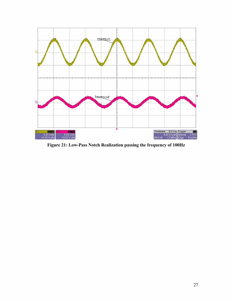
The Low-Pass design was very successful as shown in the plots in Figure 21, Figure 22,
Figure 23, and Figure 24. In these plots, the input frequency is shown in yellow, while
the output frequency is shown in pink. It is shown that as the frequency increases, the
output amplitude decreases, as designed. For example, noted in Figure 23 (400 Hz), the
amplitude is small, but the output frequency is somewhat noticeable. In Figure 24 (1
kHz) it is unrecognizable.
27
Figure 21: Low-Pass Notch Realization passing the frequency of 100Hz

28
Figure 22: Low-Pass Notch Realization passing the frequency of 200Hz

29
Figure 23: Low-Pass Notch Realization stopping the frequency of 400 Hz

30
Figure 24: Low-Pass Notch Realization stopping the frequency of 1 kHz
Finally, the actual design of our part is shown in Figure 25 and Figure 26. As seen, it is
a somewhat complex design. The design was such that the High-Pass and Band-Pass
sections were laid out the same so that debugging any potential problems in the circuit
would be universal for the 3 filters.

31
Figure 25: Overview of the final implementation of all 3 circuits on a breadboard

32
Figure 26: Up close view of the final implementation of all 3 circuits on a
breadboard

33
Appendix I: Matlab Code
a) Low-Pass Design
% Filter specifications fp = 200; % Pass band frequency edge ap = 2; % Pass band attenuation fs = 225; % Stop band frequency edge as = 17; % Stop band attenuation % Frequency Normalization kf = 2*pi*fp % Frequency scaling Factor wp = 1 % Normalized pass band frequency in Rad / Sec ws = 2*pi*fs/kf % Stop band normalized frequency % Find the order of the elliptic filter [n,wn] = ellipord (wp,ws,ap,as,'s') % Finding the transfer function % Numerator and Denominator coefficients [num,den] = ellip (n,ap,as,wn,'s') % Plotting the frequency response w = [0:.01:4]'; % Frequency Vector Rad / Sec H = Freqs (num,den,w); % Frequency Response magdb = 20*log10(abs(H)); % Magnitude Response in dB plot(w,magdb) xlabel('Freq. in rad./sec.') ylabel('Mag.,dB') grid on plot(w,-magdb); % Attenuation xlabel('Freq. in rad./sec.') ylabel('Att.,dB') grid on; % Factoring the transfer function % First and second order section [sos,g]=tf2sos(num,den)

34
b) High-Pass Design %Elliptic HP Filter Design %Attnenuation Requirements as=20 ap=0.5 wp=2*pi*7e3 ws=2*pi*6e3 kf=wp/1 wpn=wp/kf wsn=ws/kf %Finding the Order [n,wn]=ellipord(wpn, wsn,ap,as,'s'); fprintf('\n The order of the required filter is: %f',n) %Finding the Transfer Function of normalized case [num,den]=ellip(n,ap,as,wn,'high','s'); %Plot the Frequency Response w=[0:.01:3]'; H=freqs(num,den,w); magdB=20*log10(abs(H)); plot(kf*w/(2*pi),magdB) xlabel('Frequency (Hz)') ylabel('Magnitude Response (dB)') grid on plot(kf*w/(2*pi), -magdB) xlabel('Frequency (Hz)') ylabel('Attenuation (dB)') title('Attenuation Characteristics of Elliptic Filter') grid on %Factoring the Transfer Function [sos,g]=tf2sos(num,den); sos g

35
c) Band-Pass Design % Elliptic BPF Specs fsl=200; %Lower stopband in Hz wsl=2*pi*fsl; fpl=250; %Lower passband in Hz wpl=2*pi*fpl; fpu=7000; %Upper passband in Hz wpu=2*pi*fpu; fsu=7500; %Upper stopband in Hz wsu=2*pi*fsu; ap=5; %Alpha pass as=10; %Alpha stop % Frequency Normalization f0=sqrt(fpl*fpu); w0=2*pi*f0; kf=w0; wpn=[wpl wpu]/kf; wsn=[wsl wsu]/kf; % Finding order & transfer function (norm) [n,wn]=ellipord(wpn,wsn,ap,as,'s'); [num,den]=ellip(n,ap,as,wn,'s'); fprintf('\nThe order of the Elliptic BPF is: %f',n*2) fprintf('\r') %Plotting the Responses & Attenuation w=[0:0.01:7]'; %Setting a freq scale H=freqs(num,den,w); magdB=20*log10(abs(H)); subplot(2,1,1) plot(kf*w/(2*pi),magdB); %Plotting mag resp grid on; xlabel('Frequency, Hz'); ylabel('Magnitude, dB'); title('Magnitude Response'); subplot(2,1,2) plot(angle(H)); %Plotting phase resp grid on; xlabel('Frequency, Hz'); ylabel('Phase, rad'); title('Phase Response'); figure plot(kf*w/(2*pi),-magdB); %Plotting atten

36
grid on; xlabel('Frequency, Hz'); ylabel('Attenuation, dB'); title('Attenuation'); figure freqs(num,den) %Plotting freq resp tf(num,den) %Finding the transfer function [sos,g]=tf2sos(num,den) %Factoring of the trans func

37
Appendix II: Calculations for the PSPICE Design a) Low-Pass Notch Design
ω02Den 956.944=ω01Den 1.252 103
×=
ω02Den kf ω02⋅:=ω01Den kf ω01⋅:=
ωz2Den 1.323 103×=
ωz1Den 2.147 103×=
ωz2Den kf ωz2⋅:=ωz1Den kf ωz1.⋅:=
kf 1.257 103×=
kf 200 2⋅ π⋅:=
Denormalization
Q2 1.247=Q1 20.246=
Q2ω02
0.6109:=Q1
ω010.0492
:=
ω02 0.762=ω01 0.996=
ω01 0.9922:=ω02 0.5799:=
ωz2 1.053=ωz1. 1.708=
ωz1. 2.9183:=ωz2 1.1082:=
2nd Stage1st Stage
Calculations of Normalized Frequencies and Quality Factors
n 4:=
From Matlab,

38
c 2b:= 2bHs
α s2 β
α
ω0Q
s
+ c
ω02
α⋅+
s2 ω0Q
s( )+ ω02
+
≡
c β 2b c−:= 2b
α 2a c−:= cGeneric Transfer Function
a2 0.679=a1 0.597=
a2g2 c2+( )
2:=a1
g1 c1+( )2
:=
b2 0.446=b1 0.446=
b2c22
:=b1c12
:=
c2 0.891=c1 0.891=
c2 g2ωz2
2
ω022
⋅:=c1 g1ωz1.
2
ω012
⋅:=
Finding a, b, and c from GIC Circuit
g2 0.466=g1 0.303=
g2ω02
2H2j0⋅
ωz22.
:=g1ω01
2H1j0⋅
ωz1.2
:=
H2j0 0.891=H1j0 0.891=
H2j0 Hj0:=H1j0 Hj0:=
Hj0 0.794:=
Finding the DC Gain

39
C1st2 4.03 10 9−
×=C2nd2 3.213 10 9−
×=
C1st2 1 a1−( ) Cap⋅:=C2nd2 1 a2−( ) Cap⋅:=
C1st1 5.97 10 9−×=
C2nd1 6.787 10 9−×=
C1st1 a1 Cap⋅:=C2nd1 a2 Cap⋅:=
R1st5 7.334 105×=
R2nd5 9.593 105×=
R1st5R1st11 c1−( )
:=R2nd5
R2nd11 c2−( )
:=
R1st4 8.966 104×=
R2nd4 1.173 105×=
R1st4R1st1
c1:=
R2nd4R2nd1
c2:=
R1st3 2.917 106×=
R2nd3 2.349 105×=
R1st3 Q1R1st11 b1−( )
⋅:=R2nd3 Q2
R2nd11 b2−( )
⋅:=
R1st2 3.63 106×=
R2nd2 2.924 105×=
R1st2 Q1R1st1
b1⋅:=
R2nd2Q2 R2nd1⋅
b2:=
R2nd1 1.045 105×=R1st1 7.989 104
×=
R2nd11
Cap ω02Den⋅:=R1st1
1Cap ω01Den⋅
:=
Cap 10 10 9−⋅:=
Setting Up Component Values

40
b) High-Pass Notch Design
ω02Den 5.294 104×=ω01Den 4.294 104×=
ω02Den kf ω02⋅:=ω01Den kf ω01⋅:=
ωz2Den 3.745 104×=
ωz1Den 1.975 104×=
ωz2Den kf ωz2⋅:=ωz1Den kf ωz1.⋅:=
kf 4.398 104×=
kf 7 2⋅ π⋅ 103⋅:=
Denormalization
Q2 10.814=Q1 0.751=
Q2ω02
0.1113:=Q1
ω011.2993
:=
ω01 0.976= ω02 1.204=
ω02 1.4486:=ω01 0.9532:=
ωz2 0.852=ωz1. 0.449=
ωz1. 0.2017:= ωz2 0.7251:=
2nd Stage1st Stage
Calculations of Normalized Frequencies and Quality Factors
n 4:=
From Matlab,

41
c 2b:= 2bHs
α s2 β
α
ω0Q
s
+ c
ω02
α⋅+
s2 ω0Q
s( )+ ω02
+
≡
c β 2b c−:= 2b
α 2a c−:= cGeneric Transfer Function
a2 0.474=a1 0.905=
a2g2 c2+( )
2:=a1
g1 c1+( )2
:=
b2 0.158=b1 0.158=
b2c22
:=b1c12
:=
c2 0.316=c1 0.316=
c2 g2ωz2
2
ω022
⋅:=c1 g1ωz1.
2
ω012
⋅:=
Finding a, b, and c from GIC Circuit
g2 0.632=g1 1.494=
g2ω02
2H2j0⋅
ωz22.
:=g1ω01
2H1j0⋅
ωz1.2
:=
H2j0 0.316=H1j0 0.316=
H2j0 Hj0:=H1j0 Hj0:=
Hj0 0.1=
Hj0Goverall ωz1.
2ωz2
2⋅
⋅
ω012ω02
2⋅
:=
Goverall 0.9441:=
Finding the DC Gain

42
C1st2 9.468 10 10−×= C2nd2 5.26 10 9−
×=
C1st2 1 a1−( ) Cap⋅:=C2nd2 1 a2−( ) Cap⋅:=
C1st1 9.053 10 9−×=
C2nd1 4.74 10 9−×=
C1st1 a1 Cap⋅:=C2nd1 a2 Cap⋅:=
R1st5 3.406 103×=
R2nd5 2.763 103×=
R1st5R1st11 c1−( )
:=R2nd5
R2nd11 c2−( )
:=
R1st4 7.364 103×=
R2nd4 5.974 103×=
R1st4R1st1
c1:=
R2nd4R2nd1
c2:=
R1st3 2.079 103×=
R2nd3 2.426 104×=
R1st3 Q1R1st11 b1−( )
⋅:=R2nd3 Q2
R2nd11 b2−( )
⋅:=
R1st2 1.107 104×=
R2nd2 1.292 105×=
R1st2 Q1R1st1
b1⋅:=
R2nd2 Q2R2nd1
b2⋅:=
R2nd1 1.889 103×=R1st1 2.329 103
×=
R2nd11
Cap ω02Den⋅:=R1st1
1Cap ω01Den⋅
:=
Cap 10 10 9−⋅:=
Setting Up Component Values

43
c) Band-Pass Design
ω02Den 4.085 104×=
ω01Den 1.691 103×=
ω02Den kf ω02⋅:=ω01Den kf ω01⋅:=
ωz2Den 5.358 104×=
ωz1Den 1.29 103×=
ωz2Den kf ωz2⋅:=ωz1Den kf ωz1.⋅:=
kf 8.312 103×=
kf 2 π⋅ 250 7000⋅⋅:=
Denormalization
Q2 3.951=Q1 3.951=
Q2ω02
1.2438:=Q1
ω010.0515
:=
ω02 4.914=ω01 0.203=
ω01 0.0414:=ω02 24.152:=
ωz2 6.446=ωz1. 0.155=
ωz1. 0.0241:=ωz2 41.5507:=
2nd Stage1st Stage
Calculations of Normalized Frequencies and Quality Factors
n 4:=
From Matlab,
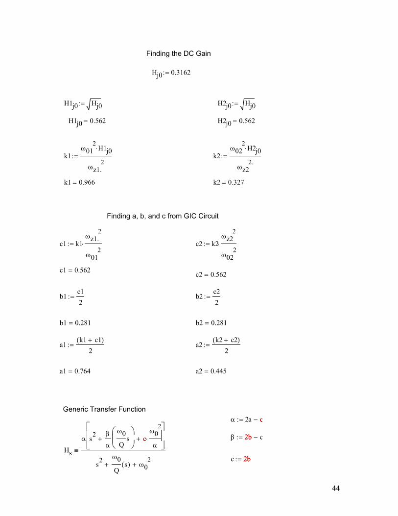
44
c 2b:= 2bHs
α s2 β
α
ω0Q
s
+ c
ω02
α⋅+
s2 ω0Q
s( )+ ω02
+
≡
c β 2b c−:= 2b
α 2a c−:= cGeneric Transfer Function
a2 0.445=a1 0.764=
a2k2 c2+( )
2:=a1
k1 c1+( )2
:=
b2 0.281=b1 0.281=
b2c22
:=b1c12
:=
c2 0.562=c1 0.562=
c2 k2ωz2
2
ω022
⋅:=c1 k1ωz1.
2
ω012
⋅:=
Finding a, b, and c from GIC Circuit
k2 0.327=k1 0.966=
k2ω02
2H2j0⋅
ωz22.
:=k1ω01
2H1j0⋅
ωz1.2
:=
H2j0 0.562=H1j0 0.562=
H2j0 Hj0:=H1j0 Hj0:=
Hj0 0.3162:=
Finding the DC Gain

45
C1st2 2.359 10 9−×= C2nd2 5.554 10 9−×=
C1st2 1 a1−( ) Cap⋅:=C2nd2 1 a2−( ) Cap⋅:=
C1st1 7.641 10 9−×=
C2nd1 4.446 10 9−×=
C1st1 a1 Cap⋅:=C2nd1 a2 Cap⋅:=
R1st5 1.351 105×= R2nd5 5.593 103×=
R1st5R1st11 c1−( )
:=R2nd5
R2nd11 c2−( )
:=
R1st4 1.052 105×=R2nd4 4.354 103
×=
R1st4R1st1
c1:=
R2nd4R2nd1
c2:=
R1st3 3.25 105×=
R2nd3 1.346 104×=
R1st3 Q1R1st11 b1−( )
⋅:=R2nd3 Q2
R2nd11 b2−( )
⋅:=
R1st2 8.309 105×=
R2nd2 3.44 104×=
R1st2 Q1R1st1
b1⋅:=
R2nd2 Q2R2nd1
b1⋅:=
R2nd1 2.448 103×=R1st1 5.913 104
×=
R2nd11
Cap ω02Den⋅:=R1st1
1Cap ω01Den⋅
:=
Cap 10 10 9−⋅:=
Setting Up Component Values

46
Appendix III: PSPICE Design a) Low-Pass Notch Design
Output to Stage 2

47
Input from Stage 1

48
b) High-Pass Notch Design Output to Stage 2

49
Input from Stage 1

50
c) Band-Pass Design
Output to Stage 2

51
Input from Stage 1

52
Appendix IV: Calculations for the MF10 a) Low-Pass Design

53

54
b) High-Pass Design

55
c) Band-Pass Design

56

57
Appendix V: MF10 Specification

MF10Universal Monolithic Dual Switched Capacitor FilterGeneral DescriptionThe MF10 consists of 2 independent and extremely easy touse, general purpose CMOS active filter building blocks.Each block, together with an external clock and 3 to 4resistors, can produce various 2nd order functions. Eachbuilding block has 3 output pins. One of the outputs can beconfigured to perform either an allpass, highpass or a notchfunction; the remaining 2 output pins perform lowpass andbandpass functions. The center frequency of the lowpassand bandpass 2nd order functions can be either directlydependent on the clock frequency, or they can depend onboth clock frequency and external resistor ratios. The centerfrequency of the notch and allpass functions is directly de-pendent on the clock frequency, while the highpass centerfrequency depends on both resistor ratio and clock. Up to 4thorder functions can be performed by cascading the two 2ndorder building blocks of the MF10; higher than 4th orderfunctions can be obtained by cascading MF10 packages.
Any of the classical filter configurations (such as Butter-worth, Bessel, Cauer and Chebyshev) can be formed.
For pin-compatible device with improved performance referto LMF100 datasheet.
Featuresn Easy to usen Clock to center frequency ratio accuracy ±0.6%n Filter cutoff frequency stability directly dependent on
external clock qualityn Low sensitivity to external component variationn Separate highpass (or notch or allpass), bandpass,
lowpass outputsn fO x Q range up to 200 kHzn Operation up to 30 kHzn 20-pin 0.3" wide Dual-In-Line packagen 20-pin Surface Mount (SO) wide-body package
System Block Diagram
01039901
Package in 20 pin molded wide body surface mount and 20 pin molded DIP.
May 2001M
F10U
niversalMonolithic
DualS
witched
Capacitor
Filter
© 2001 National Semiconductor Corporation DS010399 www.national.com
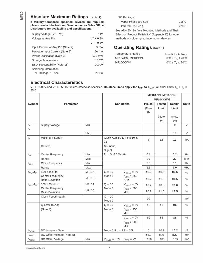
Absolute Maximum Ratings (Note 1)
If Military/Aerospace specified devices are required,please contact the National Semiconductor Sales Office/Distributors for availability and specifications.
Supply Voltage (V+ − V−) 14V
Voltage at Any Pin V+ + 0.3V
V− − 0.3V
Input Current at Any Pin (Note 2) 5 mA
Package Input Current (Note 2) 20 mA
Power Dissipation (Note 3) 500 mW
Storage Temperature 150˚C
ESD Susceptability (Note 11) 2000V
Soldering InformationN Package: 10 sec 260˚C
SO Package:
Vapor Phase (60 Sec.) 215˚C
Infrared (15 Sec.) 220˚C
See AN-450 “Surface Mounting Methods and TheirEffect on Product Reliability” (Appendix D) for othermethods of soldering surface mount devices.
Operating Ratings (Note 1)
Temperature Range TMIN ≤ TA ≤ TMAX
MF10ACN, MF10CCN 0˚C ≤ TA ≤ 70˚C
MF10CCWM 0˚C ≤ TA ≤ 70˚C
Electrical CharacteristicsV+ = +5.00V and V− = −5.00V unless otherwise specified. Boldface limits apply for T MIN to TMAX; all other limits TA = TJ =25˚C.
MF10ACN, MF10CCN,
MF10CCWM
Symbol Parameter Conditions Typical Tested Design Units
(Note8)
Limit Limit
(Note9)
(Note10)
V+ −V−
Supply Voltage Min 9 V
Max 14 V
IS Maximum Supply Clock Applied to Pins 10 &11
8 12 12 mA
Current No InputSignal
fO Center Frequency Min fO x Q < 200 kHz 0.1 0.2 Hz
Range Max 30 20 kHz
fCLK Clock Frequency Min 5.0 10 Hz
Range Max 1.5 1.0 MHz
fCLK/fO 50:1 Clock toCenter FrequencyRatio Deviation
MF10A Q = 10Mode 1
Vpin12 = 5VfCLK = 250KHz
±0.2 ±0.6 ±0.6 %
MF10C ±0.2 ±1.5 ±1.5 %
fCLK/fO 100:1 Clock toCenter FrequencyRatio Deviation
MF10A Q = 10Mode 1
Vpin12 = 0VfCLK = 500kHz
±0.2 ±0.6 ±0.6 %
MF10C ±0.2 ±1.5 ±1.5 %
Clock Feedthrough Q = 10Mode 1
10 mV
Q Error (MAX) Q = 10 Vpin12 = 5V ±2 ±6 ±6 %
(Note 4) Mode 1 fCLK = 250kHz
Vpin12 = 0V ±2 ±6 ±6 %
fCLK = 500kHz
HOLP DC Lowpass Gain Mode 1 R1 = R2 = 10k 0 ±0.2 ±0.2 dB
VOS1 DC Offset Voltage (Note 5) ±5.0 ±20 ±20 mV
VOS2 DC Offset Voltage Min Vpin12 = +5V SA/B = V+ −150 −185 −185 mV
MF1
0
www.national.com 2

Electrical Characteristics (Continued)V+ = +5.00V and V− = −5.00V unless otherwise specified. Boldface limits apply for T MIN to TMAX; all other limits TA = TJ =25˚C.
MF10ACN, MF10CCN,
MF10CCWM
Symbol Parameter Conditions Typical Tested Design Units
(Note8)
Limit Limit
(Note9)
(Note10)
(Note 5)Max (fCLK/fO =
50)−85 −85
Min Vpin12 = +5V SA/B = V− −70 mV
Max (fCLK/fO =50)
VOS3 DC Offset Voltage Min Vpin12 = +5V All Modes −70 −100 −100 mV
(Note 5)Max (fCLK/fO =
50)−20 −20
VOS2 DC Offset Voltage Vpin12 = 0V SA/B = V+ −300 mV
(Note 5) (fCLK/fO =100)
Vpin12 = 0V SA/B = V− −140 mV
(fCLK/fO =100)
VOS3 DC Offset Voltage Vpin12 = 0V All Modes −140 mV
(Note 5) (fCLK/fO =100)
VOUT Minimum Output BP, LP Pins RL = 5k ±4.25 ±3.8 ±3.8 V
Voltage SwingN/AP/HPPin
RL = 3.5k ±4.25 ±3.8 ±3.8 V
GBW Op Amp Gain BW Product 2.5 MHz
SR Op Amp Slew Rate 7 V/µs
Dynamic Range(Note 6) Vpin12 = +5V(fCLK/fO = 50)
83 dB
Vpin12 = 0V(fCLK/fO = 100)
80 dB
ISC Maximum Output Short Source 20 mA
Circuit Current(Note 7)
Sink 3.0 mA
Logic Input CharacteristicsBoldface limits apply for T MIN to TMAX; all other limits TA = TJ = 25˚C
MF10ACN, MF10CCN,
MF10CCWM
Parameter Conditions Typical Tested Design Units
(Note 8) Limit Limit
(Note 9) (Note 10)
CMOS Clock Min Logical “1” V+ = +5V, V− = −5V, +3.0 +3.0 V
Input Voltage Max Logical “0” VLSh = 0V −3.0 −3.0 V
Min Logical “1” V+ = +10V, V− = 0V, +8.0 +8.0 V
Max Logical “0” VLSh = +5V +2.0 +2.0 V
TTL Clock Min Logical “1” V+ = +5V, V− = −5V, +2.0 +2.0 V
Input Voltage Max Logical “0” VLSh = 0V +0.8 +0.8 V
MF10
www.national.com3

Logic Input Characteristics (Continued)Boldface limits apply for T MIN to TMAX; all other limits TA = TJ = 25˚C
MF10ACN, MF10CCN,
MF10CCWM
Parameter Conditions Typical Tested Design Units
(Note 8) Limit Limit
(Note 9) (Note 10)
Min Logical “1” V+ = +10V, V− = 0V, +2.0 +2.0 V
Max Logical “0” VLSh = 0V +0.8 +0.8 V
Note 1: Absolute Maximum Ratings indicate limits beyond which damage to the device may occur. DC and AC electrical specifications do not apply when operatingthe device beyond its specified operating conditions.
Note 2: When the input voltage (VIN) at any pin exceeds the power supply rails (VIN < V− or VIN > V+) the absolute value of current at that pin should be limitedto 5 mA or less. The 20 mA package input current limits the number of pins that can exceed the power supply boundaries with a 5 mA current limit to four.
Note 3: The maximum power dissipation must be derated at elevated temperatures and is dictated by TJMAX, θJA, and the ambient temperature, TA. The maximumallowable power dissipation at any temperature is PD = (TJMAX − TA)/θJA or the number given in the Absolute Maximum Ratings, whichever is lower. For this device,TJMAX = 125˚C, and the typical junction-to-ambient thermal resistance of the MF10ACN/CCN when board mounted is 55˚C/W. For the MF10AJ/CCJ, this numberincreases to 95˚C/W and for the MF10ACWM/CCWM this number is 66˚C/W.
Note 4: The accuracy of the Q value is a function of the center frequency (fO). This is illustrated in the curves under the heading “Typical PerformanceCharacteristics”.
Note 5: VOS1, VOS2, and VOS3 refer to the internal offsets as discussed in the Applications Information Section 3.4.
Note 6: For ±5V supplies the dynamic range is referenced to 2.82V rms (4V peak) where the wideband noise over a 20 kHz bandwidth is typically 200 µV rms forthe MF10 with a 50:1 CLK ratio and 280 µV rms for the MF10 with a 100:1 CLK ratio.
Note 7: The short circuit source current is measured by forcing the output that is being tested to its maximum positive voltage swing and then shorting that outputto the negative supply. The short circuit sink current is measured by forcing the output that is being tested to its maximum negative voltage swing and then shortingthat output to the positive supply. These are the worst case conditions.
Note 8: Typicals are at 25˚C and represent most likely parametric norm.
Note 9: Tested limits are guaranteed to National’s AOQL (Average Outgoing Quality Level).
Note 10: Design limits are guaranteed but not 100% tested. These limits are not used to calculate outgoing quality levels.
Note 11: Human body model, 100 pF discharged through a 1.5 kΩ resistor.
MF1
0
www.national.com 4

Typical Performance Characteristics
Power Supply Current vs. Power Supply VoltagePositive Output Voltage Swing vs. Load Resistance
(N/AP/HP Output)
0103993401039935
Negative Output Voltage Swing vs. LoadResistance
(N/AP/HP Output) Negative Output Swing vs. Temperature
01039936 01039937
Positive Output Swing vs. Temperature Crosstalk vs. Clock Frequency
0103993801039939
MF10
www.national.com5

Typical Performance Characteristics (Continued)
Q Deviation vs. Temperature Q Deviation vs. Temperature
01039940 01039941
Q Deviation vs. Clock Frequency Q Deviation vs. Clock Frequency
01039942 01039943
fCLK/fO Deviation vs. Temperature f CLK/fO Deviation vs. Temperature
01039944 01039945
MF1
0
www.national.com 6

Typical Performance Characteristics (Continued)
fCLK/fO Deviation vs. Clock Frequency f CLK/fO Deviation vs. Clock Frequency
01039946 01039947
Deviation of f CLK/fO vs. Nominal Q Deviation of f CLK/fO vs. Nominal Q
01039948 01039949
MF10
www.national.com7

Pin DescriptionsLP(1,20), BP(2,19), N/AP/HP(3,18)
The second order lowpass, bandpassand notch/allpass/highpass outputs.These outputs can typically sink 1.5 mAand source 3 mA. Each output typicallyswings to within 1V of each supply.
INV(4,17) The inverting input of the summingop-amp of each filter. These are highimpedance inputs, but the non-invertinginput is internally tied to AGND, makingINVA and INVB behave like summingjunctions (low impedance, currentinputs).
S1(5,16) S1 is a signal input pin used in theallpass filter configurations (see modes4 and 5). The pin should be driven witha source impedance of less than 1 kΩ.If S1 is not driven with a signal it shouldbe tied to AGND (mid-supply).
SA/B(6) This pin activates a switch that con-nects one of the inputs of each filter’ssecond summer to either AGND (SA/B
tied to V−) or to the lowpass (LP) output(SA/B tied to V+). This offers the flexibil-ity needed for configuring the filter in itsvarious modes of operation.
VA+(7),VD
+(8) Analog positive supply and digital posi-tive supply. These pins are internallyconnected through the IC substrate andtherefore VA
+ and VD+ should be de-
rived from the same power supplysource. They have been brought outseparately so they can be bypassed byseparate capacitors, if desired. Theycan be externally tied together and by-passed by a single capacitor.
VA−(14), VD
−(13) Analog and digital negative supplies.The same comments as for VA
+ andVD
+ apply here.
LSh(9) Level shift pin; it accommodates vari-ous clock levels with dual or single sup-ply operation. With dual ±5V supplies,the MF10 can be driven with CMOSclock levels (±5V) and the LSh pinshould be tied to the system ground. Ifthe same supplies as above are used
but only TTL clock levels, derived from0V to +5V supply, are available, theLSh pin should be tied to the systemground. For single supply operation (0Vand +10V) the VA
−, VD−pins should be
connected to the system ground, theAGND pin should be biased at +5V andthe LSh pin should also be tied to thesystem ground for TTL clock levels.LSh should be biased at +5V for CMOSclock levels in 10V single-supplyapplications.
CLKA(10), CLKB(11)Clock inputs for each switched capaci-tor filter building block. They shouldboth be of the same level (TTL orCMOS). The level shift (LSh) pin de-scription discusses how to accommo-date their levels. The duty cycle of theclock should be close to 50% especiallywhen clock frequencies above 200 kHzare used. This allows the maximumtime for the internal op-amps to settle,which yields optimum filter operation.
50/100/CL(12) By tying this pin high a 50:1clock-to-filter-center-frequency ratio isobtained. Tying this pin at mid-supplies(i.e. analog ground with dual supplies)allows the filter to operate at a 100:1clock-to-center-frequency ratio. Whenthe pin is tied low (i.e., negative supplywith dual supplies), a simple currentlimiting circuit is triggered to limit theoverall supply current down to about2.5 mA. The filtering action is thenaborted.
AGND(15) This is the analog ground pin. This pinshould be connected to the systemground for dual supply operation or bi-ased to mid-supply for single supplyoperation. For a further discussion ofmid-supply biasing techniques see theApplications Information (Section 3.2).For optimum filter performance a“clean” ground must be provided.
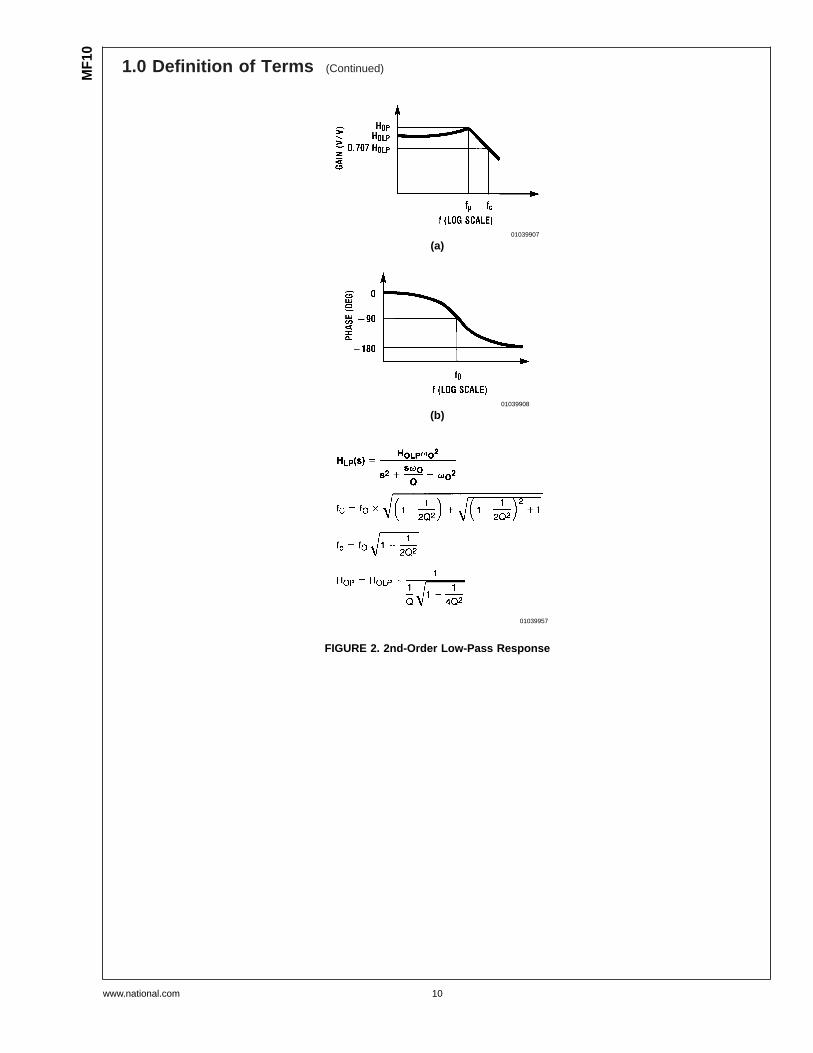
1.0 Definition of TermsfCLK: the frequency of the external clock signal applied to pin10 or 11.
fO: center frequency of the second order function complexpole pair. fO is measured at the bandpass outputs of theMF10, and is the frequency of maximum bandpass gain.(Figure 1)
fnotch : the frequency of minimum (ideally zero) gain at thenotch outputs.
fz: the center frequency of the second order complex zeropair, if any. If fz is different from fO and if QZ is high, it can beobserved as the frequency of a notch at the allpass output.(Figure 10)
Q: “quality factor” of the 2nd order filter. Q is measured at thebandpass outputs of the MF10 and is equal to fO divided by
the −3 dB bandwidth of the 2nd order bandpass filter (Figure1). The value of Q determines the shape of the 2nd orderfilter responses as shown in Figure 6.
QZ: the quality factor of the second order complex zero pair,if any. QZ is related to the allpass characteristic, which iswritten:
where QZ = Q for an all-pass response.
HOBP: the gain (in V/V) of the bandpass output at f = fO.
MF1
0
www.national.com 8

1.0 Definition of Terms (Continued)
HOLP: the gain (in V/V) of the lowpass output as f → 0 Hz(Figure 2).
HOHP: the gain (in V/V) of the highpass output as f → fCLK/2(Figure 3).
HON: the gain (in V/V) of the notch output as f → 0 Hz and asf → fCLK/2, when the notch filter has equal gain above and
below the center frequency (Figure 4). When thelow-frequency gain differs from the high-frequency gain, asin modes 2 and 3a (Figure 11 and Figure 8), the two quan-tities below are used in place of HON.
HON1: the gain (in V/V) of the notch output as f → 0 Hz.
HON2: the gain (in V/V) of the notch output as f → fCLK/2.
01039905
(a)
01039906
(b)
01039956
FIGURE 1. 2nd-Order Bandpass Response
MF10
www.national.com9
1.0 Definition of Terms (Continued)
01039907
(a)
01039908
(b)
01039957
FIGURE 2. 2nd-Order Low-Pass Response
MF1
0
www.national.com 10

1.0 Definition of Terms (Continued)
01039909
(a)
01039910
(b)
01039958
FIGURE 3. 2nd-Order High-Pass Response
MF10
www.national.com11

1.0 Definition of Terms (Continued)
01039911
(a)
01039912
(b)
01039960
FIGURE 4. 2nd-Order Notch Response
MF1
0
www.national.com 12

1.0 Definition of Terms (Continued)
01039913
(a)
01039914
(b)
01039961
FIGURE 5. 2nd-Order All-Pass Response
MF10
www.national.com13

1.0 Definition of Terms (Continued)
2.0 Modes of OperationThe MF10 is a switched capacitor (sampled data) filter. Tofully describe its transfer functions, a time domain approachis appropriate. Since this is cumbersome, and since theMF10 closely approximates continuous filters, the followingdiscussion is based on the well known frequency domain.Each MF10 can produce a full 2nd order function. See Table1 for a summary of the characteristics of the various modes.
MODE 1: Notch 1, Bandpass, Lowpass Outputs:
fnotch = fO (See Figure 7 )
fO= center frequency of the complex pole pair
fnotch= center frequency of the imaginary zero pair = fO.
= quality factor of the complex pole pair
BW = the −3 dB bandwidth of the bandpass output.
Circuit dynamics:
MODE 1a: Non-Inverting BP, LP (See Figure 8 )
Note: VIN should be driven from a low impedance (<1 kΩ) source.
(a) Bandpass (b) Low Pass (c) High-Pass
01039950 0103995101039952
(d) Notch (e) All-Pass
01039953 01039954
FIGURE 6. Response of various 2nd-order filters as a function of Q.Gains and center frequencies are normalized to unity.
MF1
0
www.national.com 14

2.0 Modes of Operation (Continued)
MODE 2: Notch 2, Bandpass, Lowpass: f notch < fO(See Figure 9 )
MODE 3: Highpass, Bandpass, Lowpass Outputs(See Figure 10 )
01039916
FIGURE 7. MODE 1
01039917
FIGURE 8. MODE 1a
MF10
www.national.com15

2.0 Modes of Operation (Continued)
01039918
FIGURE 9. MODE 2
01039919
*In Mode 3, the feedback loop is closed around the input summing amplifier; the finite GBW product of this op amp causes a slight Q enhancement. If this is aproblem, connect a small capacitor (10 pF − 100 pF) across R4 to provide some phase lead.
FIGURE 10. MODE 3
MF1
0
www.national.com 16
2.0 Modes of Operation (Continued)
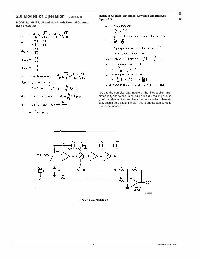
MODE 3a: HP, BP, LP and Notch with External Op Amp(See Figure 11 )
MODE 4: Allpass, Bandpass, Lowpass Outputs(SeeFigure 12 )
*Due to the sampled data nature of the filter, a slight mis-match of fz and fO occurs causing a 0.4 dB peaking aroundfO of the allpass filter amplitude response (which theoreti-cally should be a straight line). If this is unacceptable, Mode5 is recommended.
01039920
FIGURE 11. MODE 3a
MF10
www.national.com17

2.0 Modes of Operation (Continued)
MODE 5: Numerator Complex Zeros, BP, LP(See Figure 13 )
MODE 6a: Single Pole, HP, LP Filter (See Figure 14 )
MODE 6b: Single Pole LP Filter (Inverting andNon-Inverting) (See Figure 15 )
01039921
FIGURE 12. MODE 4
01039922
FIGURE 13. MODE 5
MF1
0
www.national.com 18

2.0 Modes of Operation (Continued)
TABLE 1. Summary of Modes. Realizable filter types (e.g. low-pass) denoted by asterisks.Unless otherwise noted, gains of various filter outputs are inverting and adjustable by resistor ratios.
Mode BP LP HP N AP Number of Adjustable Notes
Resistors f CLK/fO1 * * * 3 No
(2) May need input buffer.
1a HOBP1 = −Q HOLP + 1 2 No Poor dynamics for
HOBP2 = +1 high Q.
2 * * * 3 Yes (above fCLK/50
or fCLK/100)
3* * * 4 Yes Universal State-Variable
Filter. Best general-purpose mode.
3a* * * * 7 Yes As above, but also includes
resistor-tuneable notch.
4 * * * 3 No Gives Allpass response with
HOAP = −1 and HOLP = −2.
5 * * * 4 Gives flatter allpass response
than above if R1 = R2 = 0.02R4.
6a * * 3 Single pole.
6b 2 Single pole.
01039923
FIGURE 14. MODE 6a
01039924
FIGURE 15. MODE 6b
MF10
www.national.com19
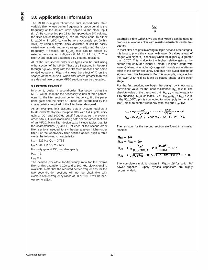
3.0 Applications InformationThe MF10 is a general-purpose dual second-order statevariable filter whose center frequency is proportional to thefrequency of the square wave applied to the clock input(fCLK). By connecting pin 12 to the appropriate DC voltage,the filter center frequency fO can be made equal to eitherfCLK/100 or fCLK/50. fO can be very accurately set (within±6%) by using a crystal clock oscillator, or can be easilyvaried over a wide frequency range by adjusting the clockfrequency. If desired, the fCLK/fO ratio can be altered byexternal resistors as in Figures 9, 10, 11, 13, 14, 15. Thefilter Q and gain are determined by external resistors.
All of the five second-order filter types can be built usingeither section of the MF10. These are illustrated in Figure 1through Figure 5 along with their transfer functions and somerelated equations. Figure 6 shows the effect of Q on theshapes of these curves. When filter orders greater than twoare desired, two or more MF10 sections can be cascaded.
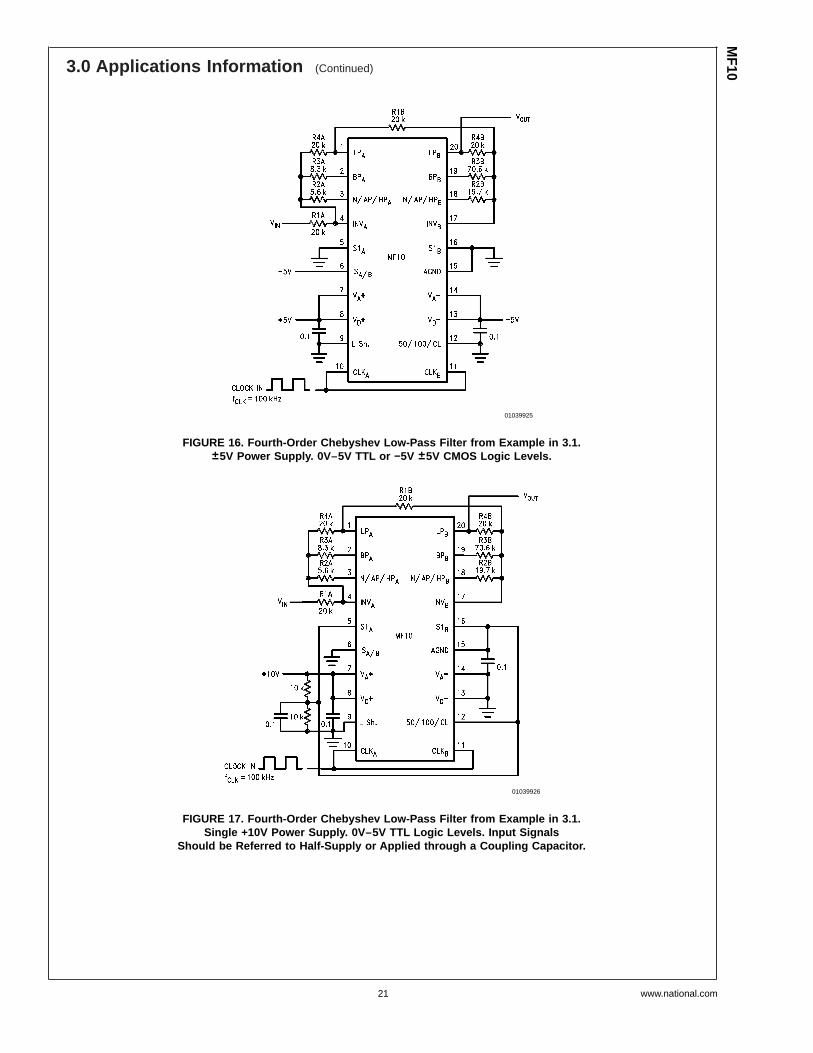
3.1 DESIGN EXAMPLE
In order to design a second-order filter section using theMF10, we must define the necessary values of three param-eters: f0, the filter section’s center frequency; H0, the pass-band gain; and the filter’s Q. These are determined by thecharacteristics required of the filter being designed.
As an example, let’s assume that a system requires afourth-order Chebyshev low-pass filter with 1 dB ripple, unitygain at DC, and 1000 Hz cutoff frequency. As the systemorder is four, it is realizable using both second-order sectionsof an MF10. Many filter design texts include tables that listthe characteristics (fO and Q) of each of the second-orderfilter sections needed to synthesize a given higher-orderfilter. For the Chebyshev filter defined above, such a tableyields the following characteristics:
f0A = 529 Hz QA = 0.785
f0B = 993 Hz QB = 3.559
For unity gain at DC, we also specify:
H0A = 1
H0B = 1
The desired clock-to-cutoff-frequency ratio for the overallfilter of this example is 100 and a 100 kHz clock signal isavailable. Note that the required center frequencies for thetwo second-order sections will not be obtainable withclock-to-center-frequency ratios of 50 or 100. It will be nec-essary to adjust
externally. From Table 1, we see that Mode 3 can be used toproduce a low-pass filter with resistor-adjustable center fre-quency.
In most filter designs involving multiple second-order stages,it is best to place the stages with lower Q values ahead ofstages with higher Q, especially when the higher Q is greaterthan 0.707. This is due to the higher relative gain at thecenter frequency of a higher-Q stage. Placing a stage withlower Q ahead of a higher-Q stage will provide some attenu-ation at the center frequency and thus help avoid clipping ofsignals near this frequency. For this example, stage A hasthe lower Q (0.785) so it will be placed ahead of the otherstage.
For the first section, we begin the design by choosing aconvenient value for the input resistance: R1A = 20k. Theabsolute value of the passband gain HOLPA is made equal to1 by choosing R4A such that: R4A = −HOLPAR1A = R1A = 20k.If the 50/100/CL pin is connected to mid-supply for nominal100:1 clock-to-center-frequency ratio, we find R2A by:
The resistors for the second section are found in a similarfashion:
The complete circuit is shown in Figure 16 for split ±5Vpower supplies. Supply bypass capacitors are highlyrecommended.
MF1
0
www.national.com 20
3.0 Applications Information (Continued)
01039925
FIGURE 16. Fourth-Order Chebyshev Low-Pass Filter from Example in 3.1.±5V Power Supply. 0V–5V TTL or −5V ±5V CMOS Logic Levels.
01039926
FIGURE 17. Fourth-Order Chebyshev Low-Pass Filter from Example in 3.1.Single +10V Power Supply. 0V–5V TTL Logic Levels. Input Signals
Should be Referred to Half-Supply or Applied through a Coupling Capacitor.
MF10
www.national.com21

3.0 Applications Information (Continued)
01039927
(a) Resistive Divider withDecoupling Capacitor
01039928
(b) Voltage Regulator
01039929
(c) Operational Amplifierwith Divider
FIGURE 18. Three Ways of Generating V +/2 for Single-Supply Operation
MF1
0
www.national.com 22

3.0 Applications Information(Continued)
3.2 SINGLE SUPPLY OPERATION
The MF10 can also operate with a single-ended power sup-ply. Figure 17 shows the example filter with a single-endedpower supply. VA
+ and VD+ are again connected to the
positive power supply (8V to 14V), and VA− and VD
− areconnected to ground. The AGND pin must be tied to V+/2 forsingle supply operation. This half-supply point should bevery “clean”, as any noise appearing on it will be treated asan input to the filter. It can be derived from the supply voltagewith a pair of resistors and a bypass capacitor (Figure 18a),or a low-impedance half-supply voltage can be made using athree-terminal voltage regulator or an operational amplifier(Figure 18b and Figure 18c). The passive resistor dividerwith a bypass capacitor is sufficient for many applications,provided that the time constant is long enough to reject anypower supply noise. It is also important that the half-supplyreference present a low impedance to the clock frequency,so at very low clock frequencies the regulator or op-ampapproaches may be preferable because they will requiresmaller capacitors to filter the clock frequency. The mainpower supply voltage should be clean (preferably regulated)and bypassed with 0.1 µF.
3.3 DYNAMIC CONSIDERATIONS
The maximum signal handling capability of the MF10, likethat of any active filter, is limited by the power supply volt-ages used. The amplifiers in the MF10 are able to swing towithin about 1V of the supplies, so the input signals must bekept small enough that none of the outputs will exceed theselimits. If the MF10 is operating on ±5V, for example, theoutputs will clip at about 8 Vp–p. The maximum input voltagemultiplied by the filter gain should therefore be less than8 Vp–p.
Note that if the filter Q is high, the gain at the lowpass orhighpass outputs will be much greater than the nominal filtergain (Figure 6). As an example, a lowpass filter with a Q of10 will have a 20 dB peak in its amplitude response at fO. Ifthe nominal gain of the filter HOLP is equal to 1, the gain at fOwill be 10. The maximum input signal at fO must therefore beless than 800 mVp–p when the circuit is operated on ±5Vsupplies.
Also note that one output can have a reasonable smallvoltage on it while another is saturated. This is most likely fora circuit such as the notch in Mode 1 (Figure 7). The notchoutput will be very small at fO, so it might appear safe toapply a large signal to the input. However, the bandpass willhave its maximum gain at fO and can clip if overdriven. If oneoutput clips, the performance at the other outputs will bedegraded, so avoid overdriving any filter section, even oneswhose outputs are not being directly used. AccompanyingFigure 7 through Figure 15 are equations labeled “circuitdynamics”, which relate the Q and the gains at the variousoutputs. These should be consulted to determine peak circuitgains and maximum allowable signals for a given applica-tion.
3.4 OFFSET VOLTAGE
The MF10’s switched capacitor integrators have a higherequivalent input offset voltage than would be found in atypical continuous-time active filter integrator. Figure 19shows an equivalent circuit of the MF10 from which theoutput DC offsets can be calculated. Typical values for theseoffsets with SA/B tied to V+ are:
Vos1 = opamp offset = ±5 mV
Vos2 = −150 mV @ 50:1: −300 mV @ 100:1
Vos3 = −70 mV @ 50:1: −140 mV @ 100:1
When SA/B is tied to V−, Vos2 will approximately halve. TheDC offset at the BP output is equal to the input offset of thelowpass integrator (Vos3). The offsets at the other outputsdepend on the mode of operation and the resistor ratios, asdescribed in the following expressions.
MF10
www.national.com23

3.0 Applications Information(Continued)
For most applications, the outputs are AC coupled and DCoffsets are not bothersome unless large signals are applied
to the filter input. However, larger offset voltages will causeclipping to occur at lower AC signal levels, and clipping at
01039930
FIGURE 19. MF10 Offset Voltage Sources
01039931
FIGURE 20. Method for Trimming V OS
MF1
0
www.national.com 24

3.0 Applications Information(Continued)
any of the outputs will cause gain nonlinearities and willchange fO and Q. When operating in Mode 3, offsets canbecome excessively large if R2 and R4 are used to makefCLK/fO significantly higher than the nominal value, especiallyif Q is also high. An extreme example is a bandpass filterhaving unity gain, a Q of 20, and fCLK/fO = 250 with pin 12tied to ground (100:1 nominal). R4/R2 will therefore be equalto 6.25 and the offset voltage at the lowpass output will beabout +1V. Where necessary, the offset voltage can beadjusted by using the circuit of Figure 20. This allows adjust-ment of VOS1, which will have varying effects on the differentoutputs as described in the above equations. Some outputscannot be adjusted this way in some modes, however(VOS(BP) in modes 1a and 3, for example).
3.5 SAMPLED DATA SYSTEM CONSIDERATIONS
The MF10 is a sampled data filter, and as such, differs inmany ways from conventional continuous-time filters. Animportant characteristic of sampled-data systems is theireffect on signals at frequencies greater than one-half thesampling frequency. (The MF10’s sampling frequency is thesame as its clock frequency.) If a signal with a frequencygreater than one-half the sampling frequency is applied tothe input of a sampled data system, it will be “reflected” to afrequency less than one-half the sampling frequency. Thus,an input signal whose frequency is fs/2 + 100 Hz will causethe system to respond as though the input frequency wasfs/2 − 100 Hz. This phenomenon is known as “aliasing”, and
can be reduced or eliminated by limiting the input signalspectrum to less than fs/2. This may in some cases requirethe use of a bandwidth-limiting filter ahead of the MF10 tolimit the input spectrum. However, since the clock frequencyis much higher than the center frequency, this will often notbe necessary.
Another characteristic of sampled-data circuits is that theoutput signal changes amplitude once every sampling pe-riod, resulting in “steps” in the output voltage which occur atthe clock rate (Figure 21). If necessary, these can be“smoothed” with a simple R–C low-pass filter at the MF10output.
The ratio of fCLK to fC (normally either 50:1 or 100:1) will alsoaffect performance. A ratio of 100:1 will reduce any aliasingproblems and is usually recommended for wideband inputsignals. In noise sensitive applications, however, a ratio of50:1 may be better as it will result in 3 dB lower output noise.The 50:1 ratio also results in lower DC offset voltages, asdiscussed in Section 3.4.
The accuracy of the fCLK/fO ratio is dependent on the valueof Q. This is illustrated in the curves under the heading“Typical Performance Characteristics”. As Q is changed, thetrue value of the ratio changes as well. Unless the Q is low,the error in fCLK/fO will be small. If the error is too large for aspecific application, use a mode that allows adjustment ofthe ratio with external resistors.
It should also be noted that the product of Q and fOshould belimited to 300 kHz when fO < 5 kHz, and to 200 kHz for fO >5 kHz.
01039932
FIGURE 21. The Sampled-Data Output Waveform
MF10
www.national.com25

3.0 Applications Information (Continued)
Connection DiagramSurface Mount and
Dual-In-Line Package
01039904
Top ViewOrder Number MF10CCWM
See NS Package Number M20BOrder Number MF10ACN or MF10CCN
See NS Package Number N20A
MF1
0
www.national.com 26

Physical Dimensions inches (millimeters)unless otherwise noted
Molded Package (Small Outline) (M)Order Number MF10ACWM or MF10CCWM
NS Package Number M20B
20-Lead Molded Dual-In-Line Package (N)Order Number MF10ACN or MF10CCN
NS Package Number N20A
MF10
www.national.com27

Notes
LIFE SUPPORT POLICY
NATIONAL’S PRODUCTS ARE NOT AUTHORIZED FOR USE AS CRITICAL COMPONENTS IN LIFE SUPPORTDEVICES OR SYSTEMS WITHOUT THE EXPRESS WRITTEN APPROVAL OF THE PRESIDENT AND GENERALCOUNSEL OF NATIONAL SEMICONDUCTOR CORPORATION. As used herein:
1. Life support devices or systems are devices orsystems which, (a) are intended for surgical implantinto the body, or (b) support or sustain life, andwhose failure to perform when properly used inaccordance with instructions for use provided in thelabeling, can be reasonably expected to result in asignificant injury to the user.
2. A critical component is any component of a lifesupport device or system whose failure to performcan be reasonably expected to cause the failure ofthe life support device or system, or to affect itssafety or effectiveness.
National SemiconductorCorporationAmericasTel: 1-800-272-9959Fax: 1-800-737-7018Email: [email protected]
National SemiconductorEurope
Fax: +49 (0) 180-530 85 86Email: [email protected]
Deutsch Tel: +49 (0) 69 9508 6208English Tel: +44 (0) 870 24 0 2171Français Tel: +33 (0) 1 41 91 8790
National SemiconductorAsia Pacific CustomerResponse GroupTel: 65-2544466Fax: 65-2504466Email: [email protected]
National SemiconductorJapan Ltd.Tel: 81-3-5639-7560Fax: 81-3-5639-7507
www.national.com
MF1
0U
nive
rsal
Mon
olith
icD
ualS
witc
hed
Cap
acito
rFi
lter
National does not assume any responsibility for use of any circuitry described, no circuit patent licenses are implied and National reserves the right at any time without notice to change said circuitry and specifications.