design of 5th-order low-pass switched capacitor elliptic...
TRANSCRIPT
Design of 5th
-Order Low-Pass Switched
Capacitor Elliptic Filter Allen Waters, ECE 626
I. INTRODUCTION
Matlab and Cadence Spectre are used to design and simulate a 5th-order low pass
switched capacitor filter, operating at 15 MHz. The entire design process is documented and the filter is designed using ideal opamps and switches, achieving 0.2dB passband ripple (0-1 MHz) and -60dB stopband attenuation (2-7.5 MHz).
The filter includes a first-order, high-Q biquad, and low-Q biquad stage, and is optimized for both dynamic range and area. Non-idealities including finite gain
and bandwidth, charge injection, slew rate, and offset voltage are simulated.
II. IDEAL DERIVATION IN MATLAB
a. Architecture survey
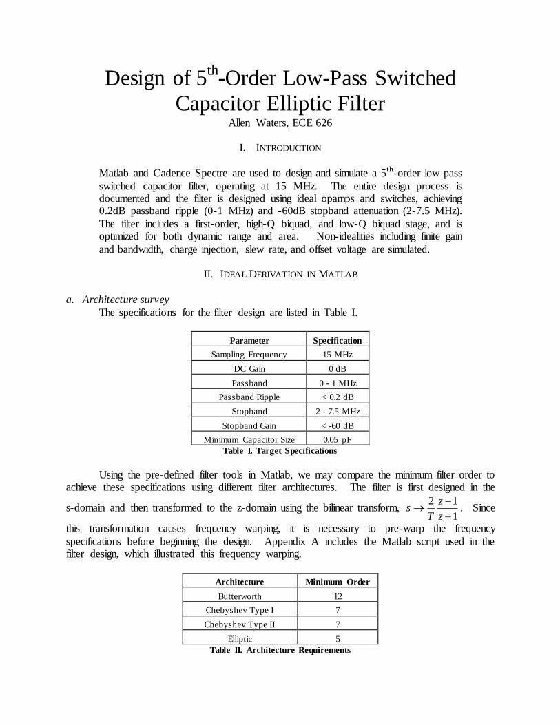
The specifications for the filter design are listed in Table I.
Parameter Specification
Sampling Frequency 15 MHz
DC Gain 0 dB
Passband 0 - 1 MHz
Passband Ripple < 0.2 dB
Stopband 2 - 7.5 MHz
Stopband Gain < -60 dB
Minimum Capacitor Size 0.05 pF
Table I. Target Specifications
Using the pre-defined filter tools in Matlab, we may compare the minimum filter order to
achieve these specifications using different filter architectures. The filter is first designed in the
s-domain and then transformed to the z-domain using the bilinear transform, 1
12
z
z
Ts . Since
this transformation causes frequency warping, it is necessary to pre-warp the frequency
specifications before beginning the design. Appendix A includes the Matlab script used in the filter design, which illustrated this frequency warping.
Architecture Minimum Order
Butterworth 12
Chebyshev Type I 7
Chebyshev Type II 7
Elliptic 5
Table II. Architecture Requirements
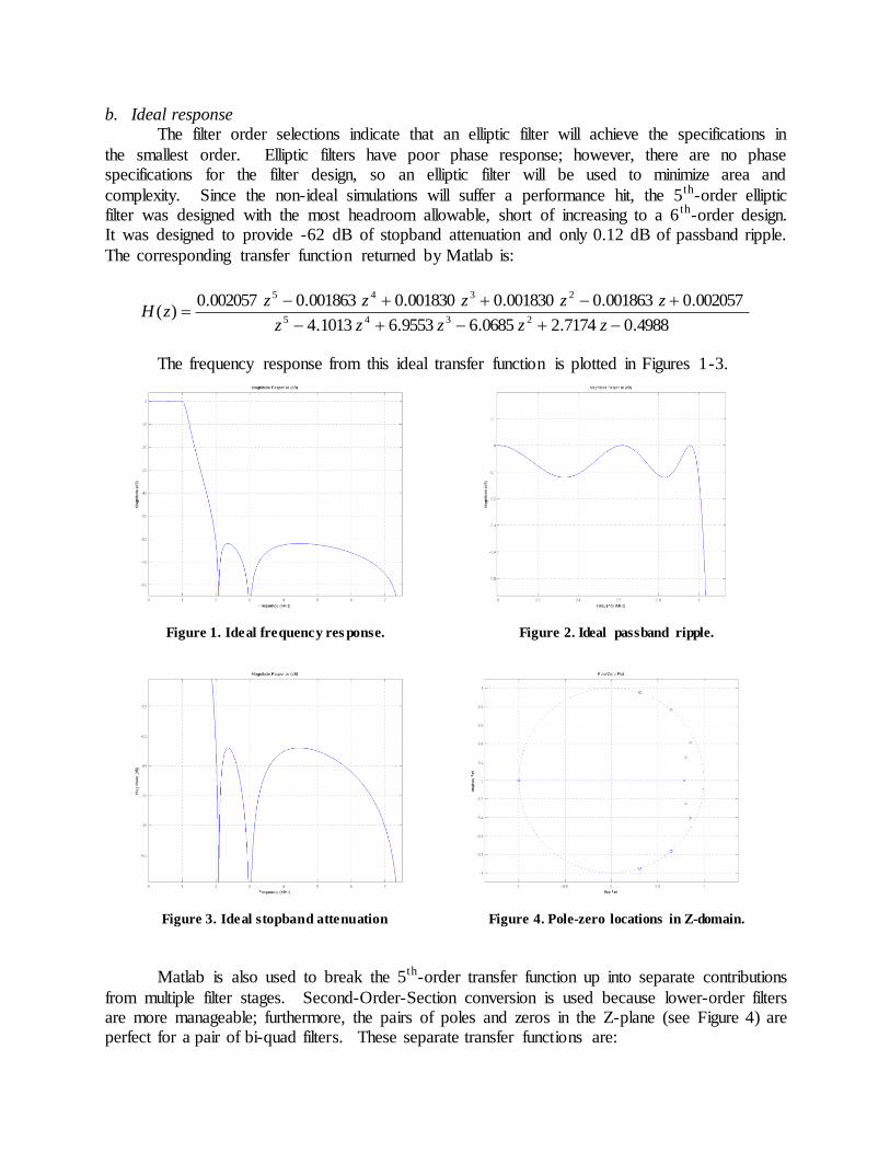
b. Ideal response The filter order selections indicate that an elliptic filter will achieve the specifications in
the smallest order. Elliptic filters have poor phase response; however, there are no phase specifications for the filter design, so an elliptic filter will be used to minimize area and
complexity. Since the non-ideal simulations will suffer a performance hit, the 5th-order elliptic filter was designed with the most headroom allowable, short of increasing to a 6 th-order design. It was designed to provide -62 dB of stopband attenuation and only 0.12 dB of passband ripple.
The corresponding transfer function returned by Matlab is:
4988.07174.20685.69553.61013.4
002057.0001863.0001830.0001830.0001863.0002057.0)(
2345
2345
zzzzz
zzzzzzH
The frequency response from this ideal transfer function is plotted in Figures 1-3.
Figure 1. Ideal frequency res ponse. Figure 2. Ideal passband ripple.
Figure 3. Ideal stopband attenuation Figure 4. Pole-zero locations in Z-domain.
Matlab is also used to break the 5th-order transfer function up into separate contributions
from multiple filter stages. Second-Order-Section conversion is used because lower-order filters are more manageable; furthermore, the pairs of poles and zeros in the Z-plane (see Figure 4) are perfect for a pair of bi-quad filters. These separate transfer functions are:

The quality factor of each filter is determined from the pole frequency, P
PQ
Re2 .
There is one high-Q stage (Q >> 1) and one low-Q stage (Q ≈ 1), as well as a first-order stage.
The Second-Order-Section conversion leaves a scalar G representing the overall gain of the system. This gain is distributed evenly among the three filter blocks. Note that this is not merely
for convenience- by minimizing the gain in any of the three stages, the difference between capacitor values is minimized. This is beneficial when the filter is scaled for area, as addressed in Section IV.
Figure 5. Cascaded filter design. Figure 6. Linear, first-order stage.
; Q = 0.5
; Q = 4.0674
; Q = 1.0063
;

Figure 7. High-Q biquad stage.
Figure 8. Low-Q biquad stage.
III. FILTER ARCHITECTURE
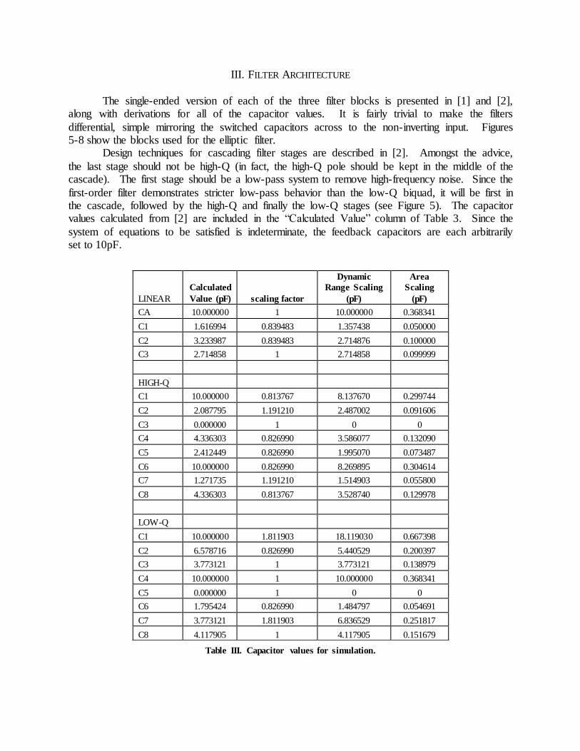
The single-ended version of each of the three filter blocks is presented in [1] and [2], along with derivations for all of the capacitor values. It is fairly trivial to make the filters
differential, simple mirroring the switched capacitors across to the non-inverting input. Figures 5-8 show the blocks used for the elliptic filter.
Design techniques for cascading filter stages are described in [2]. Amongst the advice,
the last stage should not be high-Q (in fact, the high-Q pole should be kept in the middle of the cascade). The first stage should be a low-pass system to remove high-frequency noise. Since the
first-order filter demonstrates stricter low-pass behavior than the low-Q biquad, it will be first in the cascade, followed by the high-Q and finally the low-Q stages (see Figure 5). The capacitor values calculated from [2] are included in the “Calculated Value” column of Table 3. Since the
system of equations to be satisfied is indeterminate, the feedback capacitors are each arbitrarily set to 10pF.
Table III. Capacitor values for simulation.
LINEAR
Calculated
Value (pF) scaling factor
Dynamic
Range Scaling
(pF)
Area
Scaling
(pF)
CA 10.000000 1 10.000000 0.368341
C1 1.616994 0.839483 1.357438 0.050000
C2 3.233987 0.839483 2.714876 0.100000
C3 2.714858 1 2.714858 0.099999
HIGH-Q
C1 10.000000 0.813767 8.137670 0.299744
C2 2.087795 1.191210 2.487002 0.091606
C3 0.000000 1 0 0
C4 4.336303 0.826990 3.586077 0.132090
C5 2.412449 0.826990 1.995070 0.073487
C6 10.000000 0.826990 8.269895 0.304614
C7 1.271735 1.191210 1.514903 0.055800
C8 4.336303 0.813767 3.528740 0.129978
LOW-Q
C1 10.000000 1.811903 18.119030 0.667398
C2 6.578716 0.826990 5.440529 0.200397
C3 3.773121 1 3.773121 0.138979
C4 10.000000 1 10.000000 0.368341
C5 0.000000 1 0 0
C6 1.795424 0.826990 1.484797 0.054691
C7 3.773121 1.811903 6.836529 0.251817
C8 4.117905 1 4.117905 0.151679
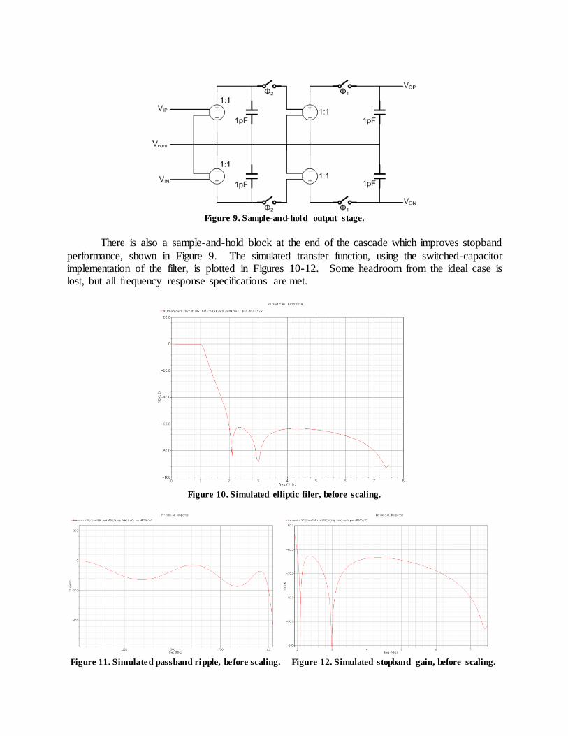
Figure 9. Sample-and-hold output stage.
There is also a sample-and-hold block at the end of the cascade which improves stopband
performance, shown in Figure 9. The simulated transfer function, using the switched-capacitor implementation of the filter, is plotted in Figures 10-12. Some headroom from the ideal case is lost, but all frequency response specifications are met.
Figure 10. Simulated elliptic filer, before scaling.
Figure 11. Simulated passband ripple, before scaling. Figure 12. Simulated stopband gain, before scaling.
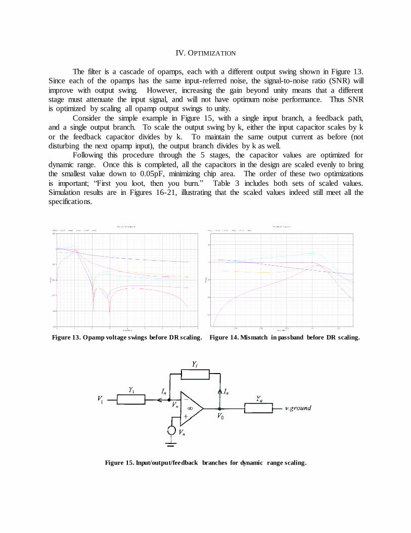
IV. OPTIMIZATION
The filter is a cascade of opamps, each with a different output swing shown in Figure 13. Since each of the opamps has the same input-referred noise, the signal-to-noise ratio (SNR) will
improve with output swing. However, increasing the gain beyond unity means that a different stage must attenuate the input signal, and will not have optimum noise performance. Thus SNR is optimized by scaling all opamp output swings to unity.
Consider the simple example in Figure 15, with a single input branch, a feedback path, and a single output branch. To scale the output swing by k, either the input capacitor scales by k
or the feedback capacitor divides by k. To maintain the same output current as before (not disturbing the next opamp input), the output branch divides by k as well.
Following this procedure through the 5 stages, the capacitor values are optimized for
dynamic range. Once this is completed, all the capacitors in the design are scaled evenly to bring the smallest value down to 0.05pF, minimizing chip area. The order of these two optimizations
is important; “First you loot, then you burn.” Table 3 includes both sets of scaled values. Simulation results are in Figures 16-21, illustrating that the scaled values indeed still meet all the specifications.
Figure 13. Opamp voltage swings before DR scaling. Figure 14. Mismatch in passband before DR scaling.
Figure 15. Input/output/feedback branches for dynamic range scaling.
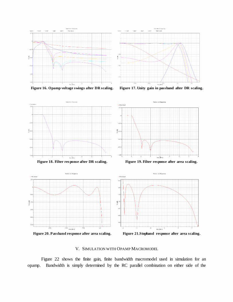
Figure 16. Opamp voltage swings after DR scaling. Figure 17. Unity gain in passband after DR scaling.
Figure 18. Filter res ponse after DR scaling. Figure 19. Filter response after area scaling.
Figure 20. Passband response after area scaling. Figure 21.Stopband response after area scaling.
V. SIMULATION WITH OPAMP MACROMODEL
Figure 22 shows the finite gain, finite bandwidth macromodel used in simulation for an
opamp. Bandwidth is simply determined by the RC parallel combination on either side of the
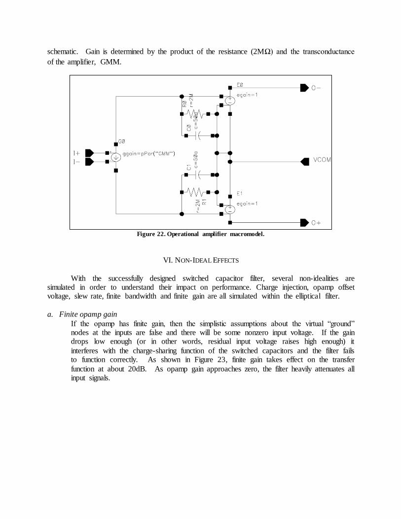
schematic. Gain is determined by the product of the resistance (2MΩ) and the transconductance
of the amplifier, GMM.
Figure 22. Operational amplifier macromodel.
VI. NON-IDEAL EFFECTS
With the successfully designed switched capacitor filter, several non-idealities are simulated in order to understand their impact on performance. Charge injection, opamp offset voltage, slew rate, finite bandwidth and finite gain are all simulated within the elliptical filter.
a. Finite opamp gain
If the opamp has finite gain, then the simplistic assumptions about the virtual “ground” nodes at the inputs are false and there will be some nonzero input voltage. If the gain drops low enough (or in other words, residual input voltage raises high enough) it
interferes with the charge-sharing function of the switched capacitors and the filter fails to function correctly. As shown in Figure 23, finite gain takes effect on the transfer
function at about 20dB. As opamp gain approaches zero, the filter heavily attenuates all input signals.

Figure 23. Effect of finite opamp gain on filter frequency response.
b. Finite opamp bandwidth Certainly, the opamp needs bandwidth at least the Nyquist rate (15MHz in this case) to
resolve an input signal. If bandwidth drops below the Nyquist rate then the passband shrinks and the transfer function loses its shape, as shown in Figures 24-26. The difference between the 100MHz and 1MHz simulations illustrates this point.
Figure 24. Effect of finite opamp bandwidth on filter frequency response.

Figure 25. Passband response with finite BW. Figure 26. Stopband response with finite BW.
c. Opamp offset voltage
Input offset is simulated by placing a DC voltage source into on of the opamp input terminals. It is generally a model for mismatch or asymmetry between the two differential paths. Similar to the residual charge from finite gain, this degrades
performance. Tens of millivolts will completely distort the filter’s frequency response.
d. Charge Injection When using real NMOS transmission gate switches, some small amount of charge is injected into the channel on each clock cycle. The charge is proportional to the area of
the device and the overdrive voltage:
VWLCQ OXinj
This is simulated using a CMOS transmission gate as shown in Figure X:
Figure 27. CMOS transmission gate for charge injection.
e. Slew rate In the ideal case, the output of the filter would respond instantaneously to stimuli at the input. Naturally, there is some duration of time while the output is still changing. Slew
rate measures this worst case rate of change of the output voltage- it is simulated by sending an ideal pulse into the filter during a transient analysis (see Figure 28). In the

output waveform, the output changes linearly trying to adapt to the ideal pulse. This is shown in Figure 29, and the calculated slew rate is 1.802 V/mS.
Figure 28. Transient simulation of slew rate. Figure 29. Detailed view of output slewing.
VII. CONCLUSION
A 5th-order low pass switched capacitor filter was designed using Matlab and Spectre.
The filter is designed using ideal opamps and switches, achieving 0.2dB passband ripple (0-1 MHz) and -60dB stopband attenuation (2-7.5 MHz) at 15 MHz sampling rate. The
filter includes a first-order, high-Q biquad, and low-Q biquad stage, and is optimized for both dynamic range and area. The area is minimized to be equivalent to a single 3.54pF capacitor. Non-idealities in the opamp and transmission gates, including finite gain and
bandwidth, charge injection, slew rate, and offset voltage, are discusses and simulated.
REFERENCES
[1] David A. Johns, and Ken Martin, “Analog Integrated Circuit Design,” John Wiley and Sons, 1997.
[2] Dr. Gabor Temes, Oregon State University, ECE626 lecture notes, Winter 2011.
APPENDIX A: MATLAB SCRIPT
function designer(gP, gS)
%Final project script for ECE626. Written by Allen Waters.
%Input parameters:
% gP: maximum passband ripple
% gS: minimum stopband attenuation

% constants
fs = 15e6; %sampling frequency
fP = 1e6; %passband frequency
fS = 2e6; %stopband frequency
% frequency warping
wP = 2*fs*tan(2*pi*fP/(2*fs));
wS = 2*fs*tan(2*pi*fS/(2*fs));
% find minimum order for different filter types
n_butter = buttord(wP, wS, gP, gS, 's');
n_cheb1 = cheb1ord(wP, wS, gP, gS, 's');
n_cheb2 = cheb2ord(wP, wS, gP, gS, 's');
[n_ellip, Wp] = ellipord(wP, wS, gP, gS, 's');
fprintf('Filter orders (butterworth, cheb1, cheb2, elliptic) are:\n')
fprintf('\t\t\t%d\t%d\t%d\t%d\n\n', n_butter, n_cheb1, n_cheb2, n_ellip)
% determine elliptic filter transfer function
[Hnum, Hden] = ellip(n_ellip, gP, gS, Wp, 'low', 's');
[HnumZ, HdenZ] = bilinear(Hnum, Hden, fs);
fvtool(HnumZ, HdenZ);
% break into three different transfer functions
[sos, gain] = tf2sos(HnumZ, HdenZ)
fprintf('Total gain needed is %f\n', gain)
g_stage = gain ^ (1/3);
fprintf('Gain per stage is %f\n', g_stage)
% calculate Q values
pole2 = roots([sos(2,4), sos(2,5), sos(2,6)]);
pole2_s = log(pole2(1));
Q2 = abs(pole2_s) / (2 * abs(real(pole2_s)));
fprintf('Q2 is %f\n', Q2)
pole3 = roots([sos(3,4), sos(3,5), sos(3,6)]);
pole3_s = log(pole3(1));
Q3 = abs(pole3_s) / (2 * abs(real(pole3_s)));
fprintf('Q3 is %f\n', Q3)
% calculate coefficients for capacitor values
% linear
fprintf('\nLINEAR STAGE\n\n')
Ca = 10;
pole1 = roots([sos(1,4), sos(1,5)]);
C3 = Ca * (1- pole1) / pole1;
dc_gain = g_stage * (sos(1,1) * 1 + sos(1,2)) / (sos(1,4) * 1 + sos(1,5));
C2 = -1 * C3 * dc_gain;
C1 = -0.5 * C2;
fprintf('Ca = %f pF\n', Ca)
fprintf('C1 = %f pF\n', C1)
fprintf('C2 = %f pF\n', C2)
fprintf('C3 = %f pF\n', C3)
% low-Q
fprintf('\nLOW-Q BIQUAD\n\n')
a2 = g_stage * sos(2,1) / sos(2,6);

a1 = g_stage * sos(2,2) / sos(2,6);
a0 = g_stage * sos(2,3) / sos(2,6);
b2 = sos(2,4) / sos(2,6);
b1 = sos(2,5) / sos(2,6);
K6 = b2 - 1;
K5 = (b1 + b2 + 1) ^ 0.5;
K4 = K5;
K3 = a0;
K2 = a2 - a0;
K1 = (a0 + a1 + a2) / K5;
C1 = 10;
C4 = 10;
fprintf('C1 = %f pF\n', C1)
fprintf('C2 = %f pF\n', K1 * C1)
fprintf('C3 = %f pF\n', K4 * C1)
fprintf('C4 = %f pF\n', C4)
fprintf('C5 = %f pF\n', K2 * C4)
fprintf('C6 = %f pF\n', K3 * C4)
fprintf('C7 = %f pF\n', K5 * C4)
fprintf('C8 = %f pF\n', K6 * C4)
% high-Q
fprintf('\nHIGH-Q BIQUAD\n\n')
a2 = g_stage * sos(3,1) / sos(3,4);
a1 = g_stage * sos(3,2) / sos(3,4);
a0 = g_stage * sos(3,3) / sos(3,4);
b1 = sos(3,5) / sos(3,4);
b0 = sos(3,6) / sos(3,4);
K5 = (b0 + b1 + 1) ^ 0.5;
K4 = K5;
K6 = (1 - b0) / K5;
K3 = a2;
K2 = (a2 - a0) / K5;
K1 = (a0 + a1 + a2) / K5;
C1 = 10;
C6 = 10;
fprintf('C1 = %f pF\n', C1)
fprintf('C2 = %f pF\n', K1 * C1)
fprintf('C3 = %f pF\n', K2 * C1)
fprintf('C4 = %f pF\n', K4 * C1)
fprintf('C5 = %f pF\n', K6 * C1)
fprintf('C6 = %f pF\n', C6)
fprintf('C7 = %f pF\n', K3 * C6)
fprintf('C8 = %f pF\n', K5 * C6)