high performance rf / if component solutions · rf modulator 800-2500 mhz 1º phase 0.2db amp...
TRANSCRIPT
RF IF
Analog DevicesConfidential Information
High Performance RF / IF Component Solutions
High Performance RF / IF Component Solutions
ANALOGDEVICES
RF/IF Standard ProductsRF/IF Standard Products
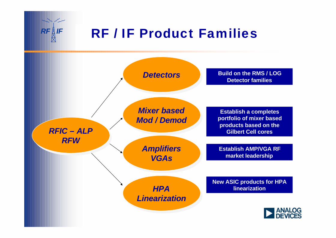
RF IF RF / IF Product Families
RFIC – ALP RFW
RFIC – ALP RFW
HPA Linearization
HPA Linearization
DetectorsDetectors
Mixer basedMod / DemodMixer basedMod / Demod
Amplifiers VGAs
Amplifiers VGAs
Build on the RMS / LOG Detector families
Establish a completes portfolio of mixer based products based on the
Gilbert Cell cores
Establish AMP/VGA RF market leadership
New ASIC products for HPA linearization
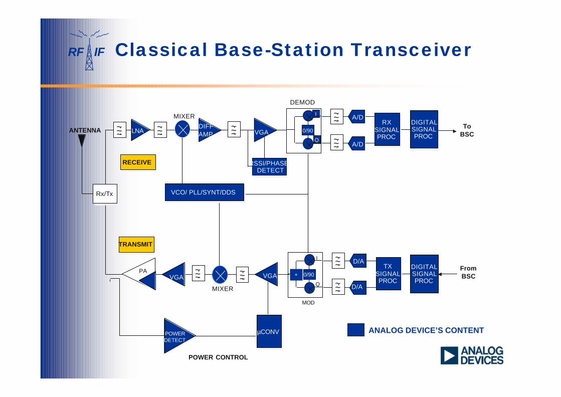
RF IF Classical Base-Station Transceiver
LNA
VCO/ PLL/SYNT/DDSVCO/ PLL/SYNT/DDS
POWER CONTROL
TRANSMITTRANSMIT
~~~
RECEIVERECEIVE
Rx/TxRx/Tx
DIFFAMP
~~~~~~
MIXER
VGA
RSSI/PHASEDETECT
RSSI/PHASEDETECT
ToBSC
DEMOD
I
Q
0/90
~~~
~~~
A/D
A/D
RXSIGNALPROC
RXSIGNALPROC
DIGITALSIGNALPROC
DIGITALSIGNALPROC
ANTENNA
FromBSC
MOD
I
Q
0/90
~~~
~~~
D/A
D/A
TXSIGNALPROC
TXSIGNALPROC
DIGITALSIGNALPROC
DIGITALSIGNALPROC
+
µCONV
VGA
POWERDETECT
~~~MIXER
~~~VGAPA
ANALOG DEVICE’S CONTENT

RF IF
DetectorsDetectors
TruPwrDetectorsTruPwr
DetectorsLogarithmic Detectors
Logarithmic Detectors
Detectors
ADI offers the industry’s broadest range RF / IF detectors
RF IF
ADC
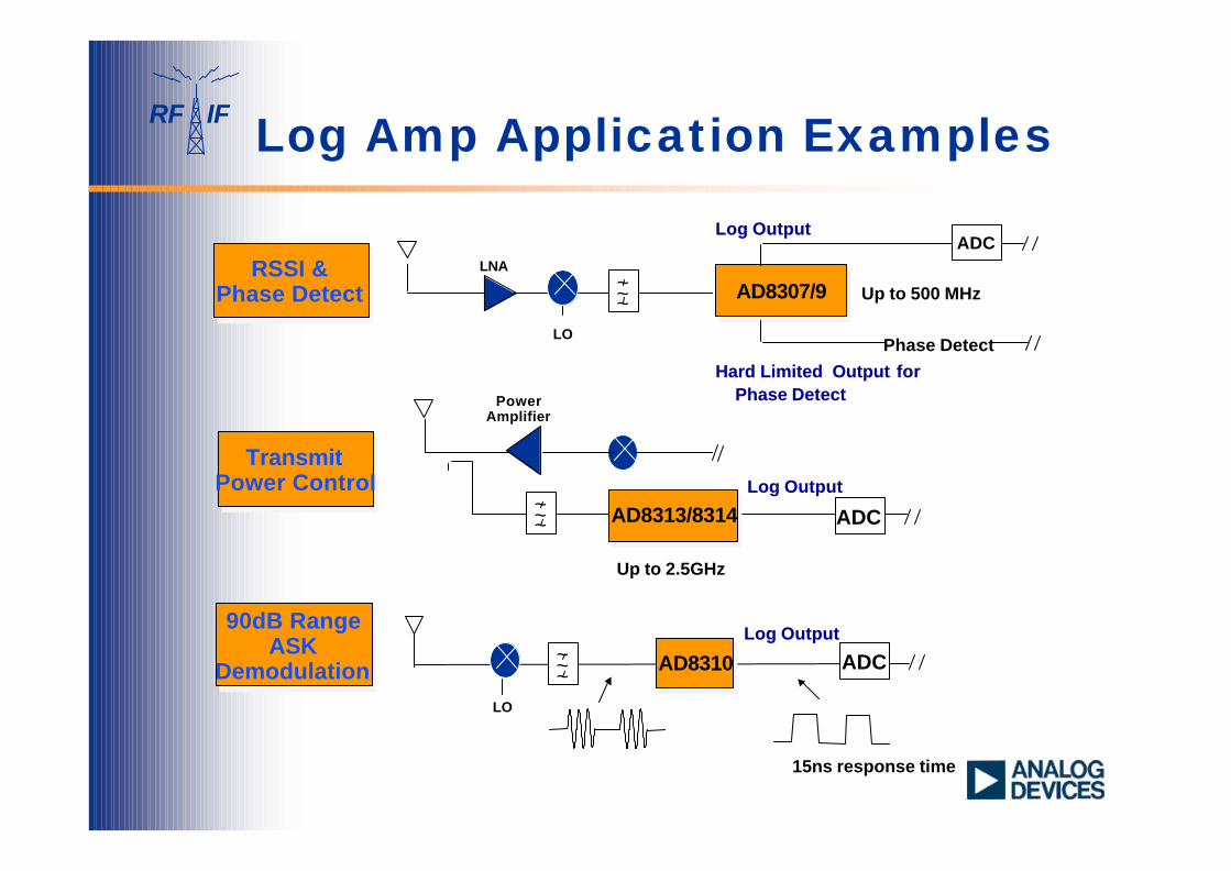
Log Amp Application Examples
LNA
PowerAmplifier
TransmitPower Control
TransmitPower Control
AD8313/8314AD8313/8314 ADC
Up to 2.5GHz
LO
AD8307/9AD8307/9
Phase Detect
Up to 500 MHzRSSI &
Phase DetectRSSI &
Phase Detect
Hard Limited OutputHard Limited Output for for Phase Detect Phase Detect
Log OutputLog Output
Log OutputLog Output~~~
~~~
LO
AD8310AD8310~~~ADC
90dB RangeASK
Demodulation
90dB RangeASK
Demodulation
15ns response time
Log OutputLog Output
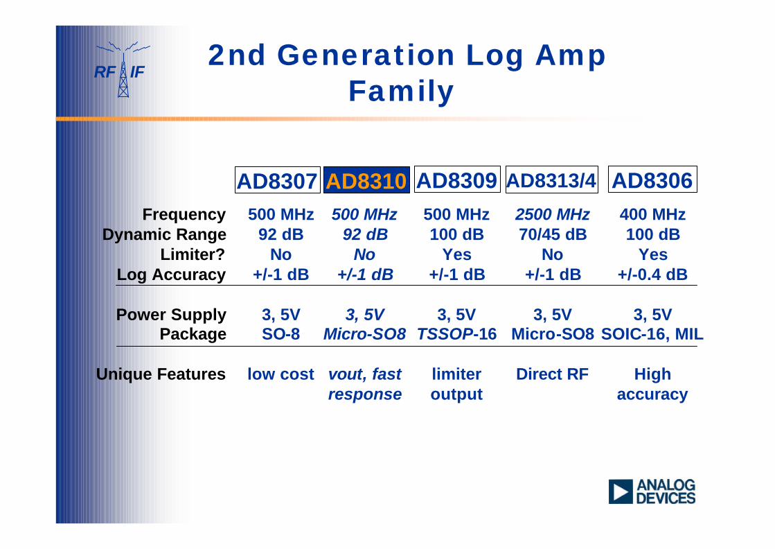
RF IF2nd Generation Log Amp
Family
FrequencyDynamic Range
Limiter?Log Accuracy
Power SupplyPackage
Unique Features
AD8309 AD8313/4AD8307500 MHz
92 dBNo
+/-1 dB
3, 5VSO-8
low cost
500 MHz100 dB
Yes+/-1 dB
3, 5VTSSOP-16
limiteroutput
2500 MHz70/45 dB
No+/-1 dB
3, 5VMicro-SO8
Direct RF
AD8306400 MHz100 dB
Yes+/-0.4 dB
3, 5VSOIC-16, MIL
Highaccuracy
500 MHz92 dB
No+/-1 dB
3, 5VMicro-SO8
vout, fast response
AD8310

RF IF
INPUT AMPLITUDE dBm
2.0
7 0
VOUT Volts
1.8
1.6
1.4
1.2
1.0
0.8
0.6
0.4
0.2
0 6 0 50 40 3 0 2 0 10 0 10
VS = +5VINPUT MATCH SHOWN IN FIGURE 27
5
4
3
2
1
0
1
2
3
4
5
ERROR dB
+25 C
+85 C
40 C
SLOPE AND INTERCEPT NORMALIZED AT +25 CAND APPLIED TO 40 C AND +85 C
AD8313 - Dynamic Range 65dB at 900MHz
to 2.5 GHz
Vout and Errorat 900 MHz
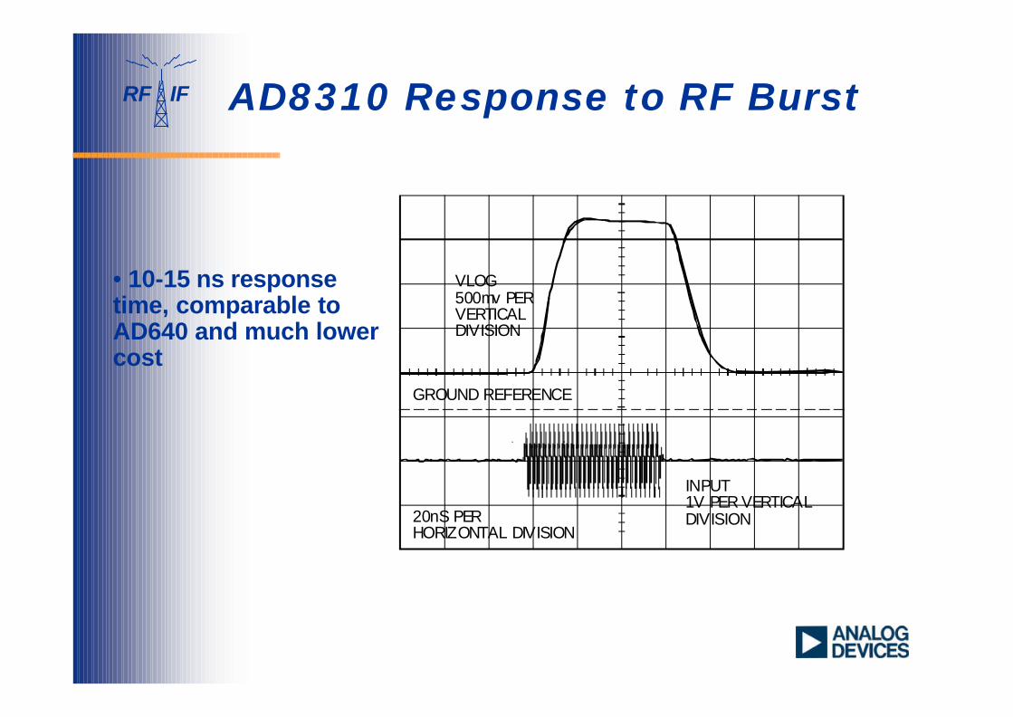
RF IF AD8310 Response to RF Burst
VLOG500mv PERVERTICALDIVISION
GROUND REFERENCE
20nS PERHORIZONTAL DIVISION
INPUT1V PER VERTICALDIVISION
• 10-15 ns response time, comparable to AD640 and much lower cost
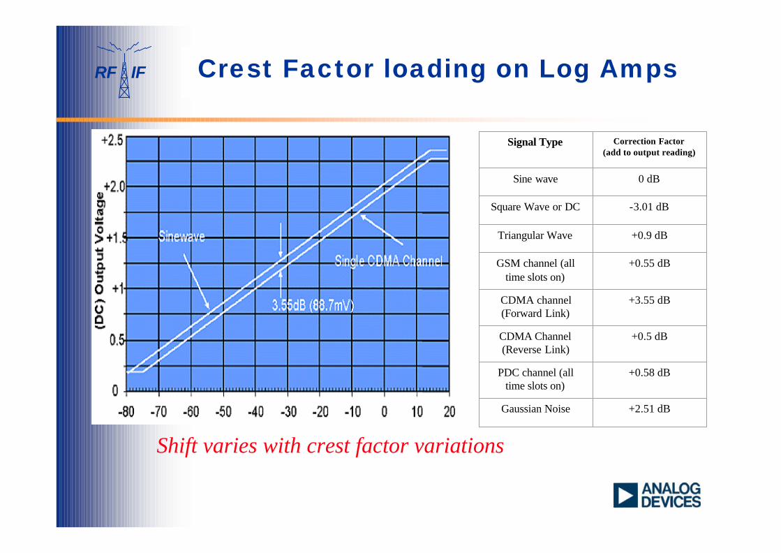
RF IF Crest Factor loading on Log Amps
Shift varies with crest factor variations
Signal Type Correction Factor(add to output reading)
Sine wave 0 dB
Square Wave or DC -3.01 dB
Triangular Wave +0.9 dB
GSM channel (all time slots on)
+0.55 dB
CDMA channel(Forward Link)
+3.55 dB
CDMA Channel (Reverse Link)
+0.5 dB
PDC channel (all time slots on)
+0.58 dB
Gaussian Noise +2.51 dB
RF IF
– Operation to 2.5 GHz– 30dB Dynamic Range– 0.3dB Accuracy for 15dB range
over temperature– Modulation Independent
(GSM/CDMA/AMPS/..)– Low Power single supply 3-5 Volts– EDN product of year 2000
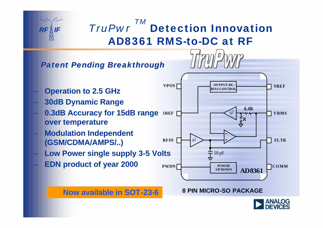
TruPwrTM
Detection Innovation AD8361 RMS-to-DC at RF
8 PIN MICRO-SO PACKAGE
X2 +
OUTPUT DCBIAS CONTROL
X2
POWERUP/DOWN AD8361
VPOS
IREF
RFIN
PWDN
SREF
VRMS
FLTR
CO MM
50 pF
R
6.4R
Patent Pending BreakthroughPatent Pending Breakthrough
Now available in SOT-23-6

RF IF AD8361 Performance
0 0.1 0.2 0.3 0.4 0.5 0.6 0.7 0.8 0.9 10
0.5
1
1.5
2
2.5
3
3.5
4
4.5
5
LEGENDIS95 rever se l ink, 1900MHz
-30 degC-40257085
RFIN - Vrms
IS-95 Reverse Link over Temperature
– 0.3dB accuracy over top 14dB, over temp
– EDGE, CDMA, QAM Solution
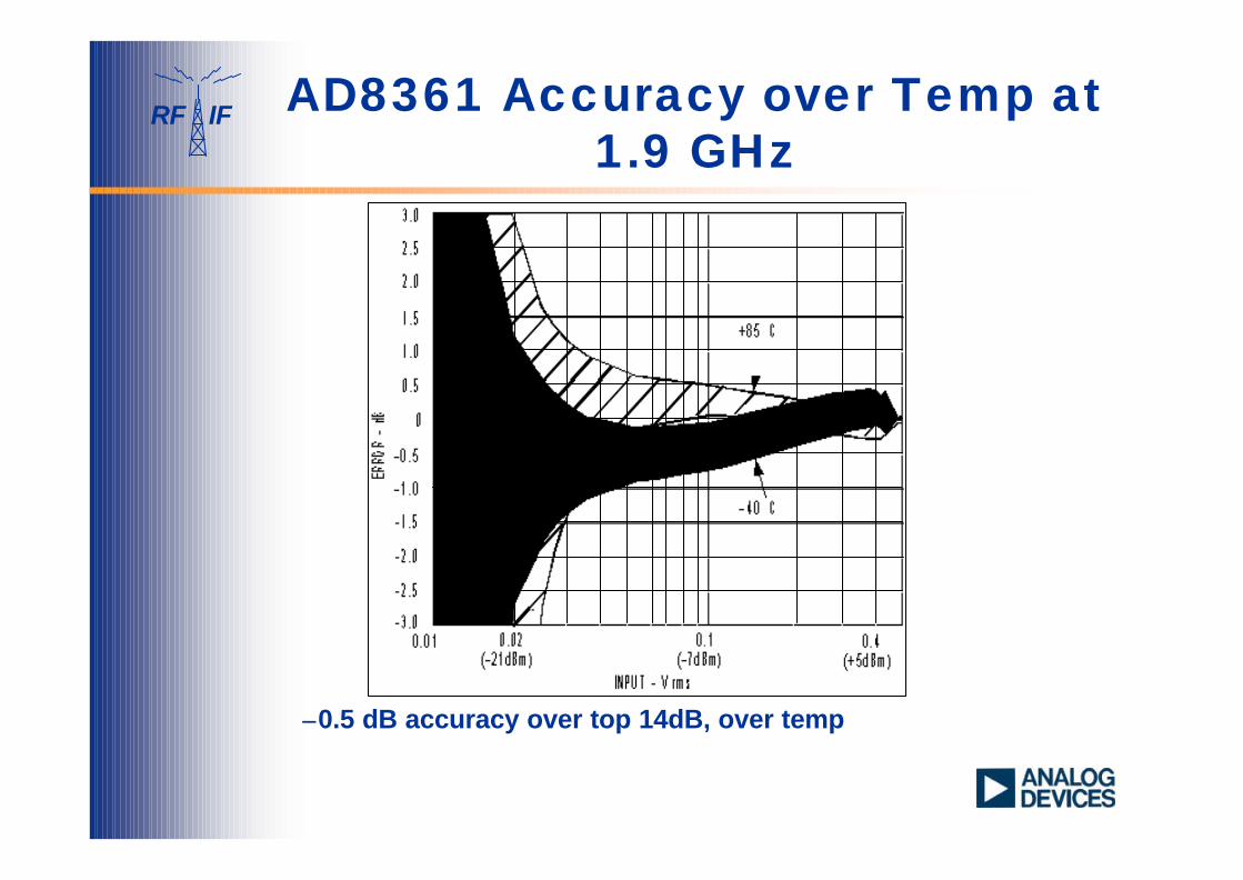
RF IF AD8361 Accuracy over Temp at 1.9 GHz
±0.5 dB accuracy over top 14dB, over temp

RF IF
x2
VIN(t)VOUT
+-
ERRORAMPLIFIERx2
SET-POINTINTERFACE
(OPTIONAL EXT FILTER)
VSET
CL
WIDEBANDSQUARERS
NULL
DCREF
VGA
50-dBRANGE
FIXEDLEVEL
AVERAGINGOCCURS HERE
GAINCONTROL
• Features– Operation to 2.5 GHz– 50dB Dynamic Range– 1dB Accuracy– Modulation Independent
(GSM/CDMA/AMPS/..)– TSSOP package– In Design - Samples Sept01
AD8362 50dB TruPwr Detector RMS-to-DC at RF
Patent Pending Patent Pending BreakthroughBreakthrough
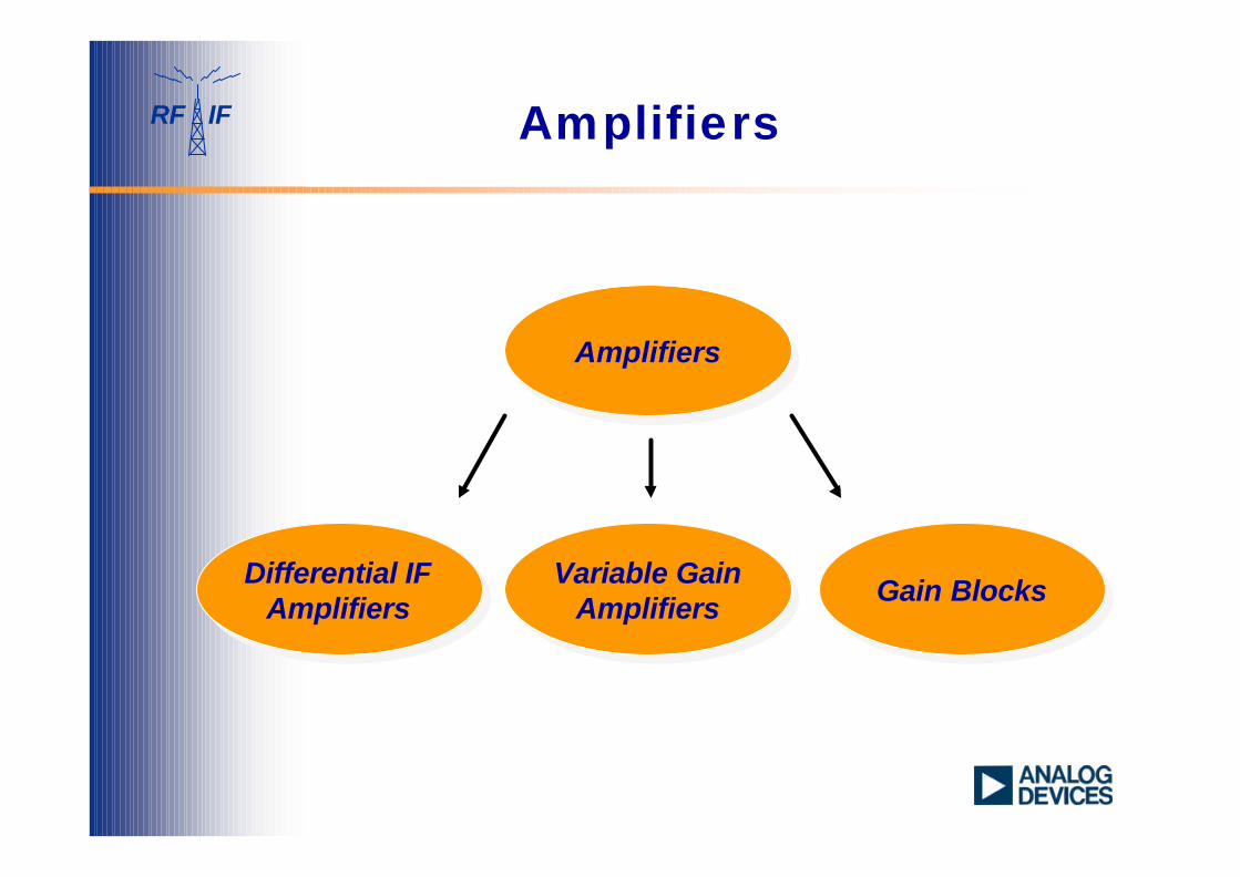
RF IF Amplifiers
Variable Gain Amplifiers
Variable Gain Amplifiers
Differential IF Amplifiers
Differential IF Amplifiers Gain BlocksGain Blocks
AmplifiersAmplifiers
RF IF
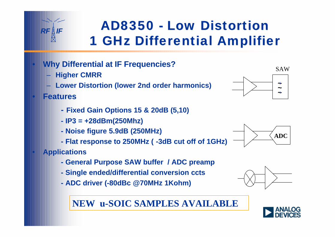
• Why Differential at IF Frequencies?– Higher CMRR– Lower Distortion (lower 2nd order harmonics)
• Features
- Fixed Gain Options 15 & 20dB (5,10)- IP3 = +28dBm(250Mhz)- Noise figure 5.9dB (250MHz) - Flat response to 250MHz ( -3dB cut off of 1GHz)
• Applications- General Purpose SAW buffer / ADC preamp- Single ended/differential conversion ccts- ADC driver (-80dBc @70MHz 1Kohm)
AD8350 AD8350 -- Low DistortionLow Distortion1 GHz Differential Amplifier1 GHz Differential Amplifier
~~~
SAW
ADC
NEW u-SOIC SAMPLES AVAILABLE
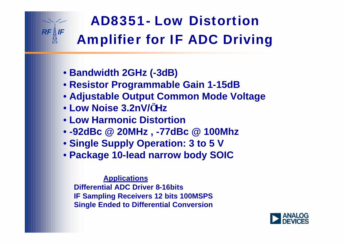
RF IFAD8351- Low Distortion
Amplifier for IF ADC Driving
• Bandwidth 2GHz (-3dB)• Resistor Programmable Gain 1-15dB• Adjustable Output Common Mode Voltage• Low Noise 3.2nV/√Hz• Low Harmonic Distortion • -92dBc @ 20MHz , -77dBc @ 100Mhz• Single Supply Operation: 3 to 5 V• Package 10-lead narrow body SOIC
ApplicationsDifferential ADC Driver 8-16bitsIF Sampling Receivers 12 bits 100MSPSSingle Ended to Differential Conversion

RF IF AD8367LF-500MHz, 45-dB VGA
l Linear dB Gain Range: -2.5 to 42.5dB l Bandwidth: 500MHzl Gain conformance: +/-0.5dBl Integrated RMS Detectorl Two Selectable Modes of Operation
l VGA Mode / AGC Mode (RSSI, Vout=500mVrms)l OIP3: 29 dBm @ 50 MHz, R1=200Ωl NF: 8 dB @ max gain, Rs=200Ωl Single-ended I/O (200Ω Input Impedance)l Single Supply Operation 2.7 – 5.5V, 20mAl Power down capability
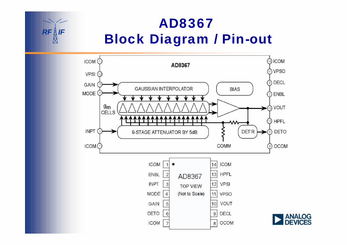
RF IFAD8367
Block Diagram / Pin-out

RF IFAD8367
Noise Figure and Linearity
Gain (dB)
-2.5
53
0 42.5
NF (dB)
8
~ 1 dB/dB
Gain (dB)
-2.5
29
0 42.5
IIP3 (dBm)
~ 1 dB/dB
OIP3
Gain (dB)

RF IF AD8367Modes of Operation
VGAIN is the RSSI output VGAIN (V)
-2.5
42.5
01
Gain (dB)
20 mV/dB
VGA ModeAGC Mode
.06
VGAIN is an input
ENBL HPFL
VPSO
ICOM
INPT
MODE
GAIN
DETO
ICOM
ICOM
VPSI
VOUT
DECL
OCOM
AD
8367
ENBL HPFL
VPSO
ICOM
INPT
MODE
GAIN
DETO
ICOM
ICOM
VPSI
VOUT
DECL
OCOM
AD
8367
COMM
VGAINVPOS
VGAIN
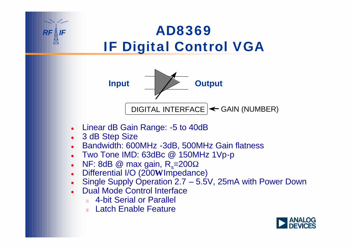
RF IF AD8369IF Digital Control VGA
l Linear dB Gain Range: -5 to 40dB l 3 dB Step Sizel Bandwidth: 600MHz -3dB, 500MHz Gain flatnessl Two Tone IMD: 63dBc @ 150MHz 1Vp-pl NF: 8dB @ max gain, Rs=200Ωl Differential I/O (200Ω Impedance)l Single Supply Operation 2.7 – 5.5V, 25mA with Power Downl Dual Mode Control Interface
3 4-bit Serial or Parallel3 Latch Enable Feature
Input Output
DIGITAL INTERFACE GAIN (NUMBER)

RF IF Mixers/Mod/Demod
Mixer basedMod / DemodMixer basedMod / Demod
Active Mixers Active Mixers DemodulatorsDemodulatorsModulatorsModulators
RF IF
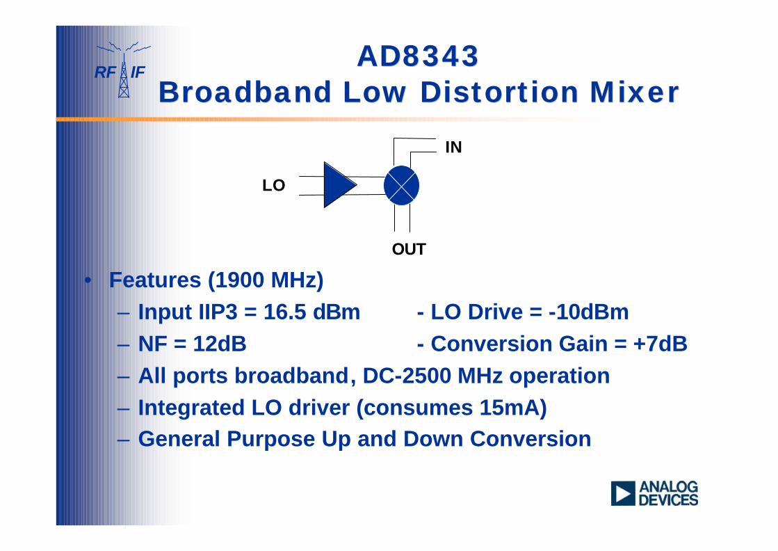
• Features (1900 MHz)– Input IIP3 = 16.5 dBm - LO Drive = -10dBm– NF = 12dB - Conversion Gain = +7dB– All ports broadband, DC-2500 MHz operation– Integrated LO driver (consumes 15mA)– General Purpose Up and Down Conversion
AD8343AD8343Broadband Low Distortion MixerBroadband Low Distortion Mixer
OUT
IN
LO
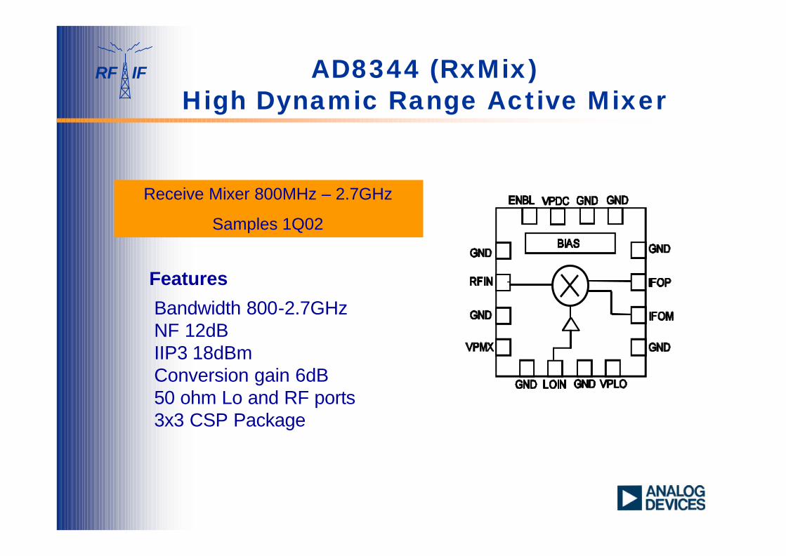
RF IF AD8344 (RxMix)High Dynamic Range Active Mixer
Bandwidth 800-2.7GHzNF 12dBIIP3 18dBmConversion gain 6dB50 ohm Lo and RF ports3x3 CSP Package
Receive Mixer 800MHz – 2.7GHz
Samples 1Q02
Features
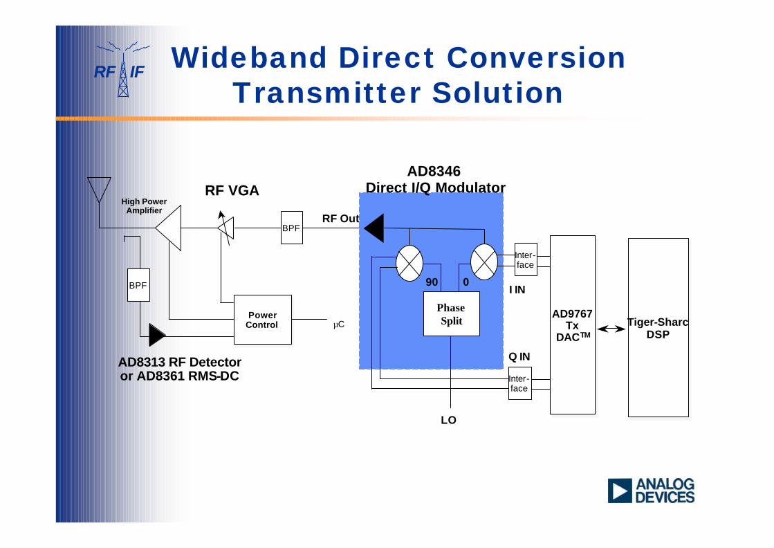
RF IF
PowerControlPower
Control
BPF
High PowerAmplifier
RF VGA
AD9767Tx
DACTM
AD9767Tx
DACTMµC
AD8313 RF Detectoror AD8361 RMS-DC
LO
AD8346Direct I/Q Modulator
PhaseSplit
Q IN
I IN
RF Out
90 0
Wideband Direct Conversion Transmitter Solution
BPF
Inter-face
Inter-face
Tiger-SharcDSP
Tiger-SharcDSP

RF IF AD8346 2.5GHz Direct I/Q Modulator
• Direct I/Q to 800-2500 MHz • DC-70 MHz I&Q Inputs• 1 deg phase error / 0.2 dB amplitude balance • -35dBc Sideband Suppression• -42dBm LO Feedthrough• -10 dBm Pout• -147dBm/Hz Noise Floor
PhaseSplit
Q IN I IN
RF90 0
LO
Matched 50 ohm output Lowest cost / power
solution

RF IF AD8346 W-CDMA Performance
-60dBc ACP
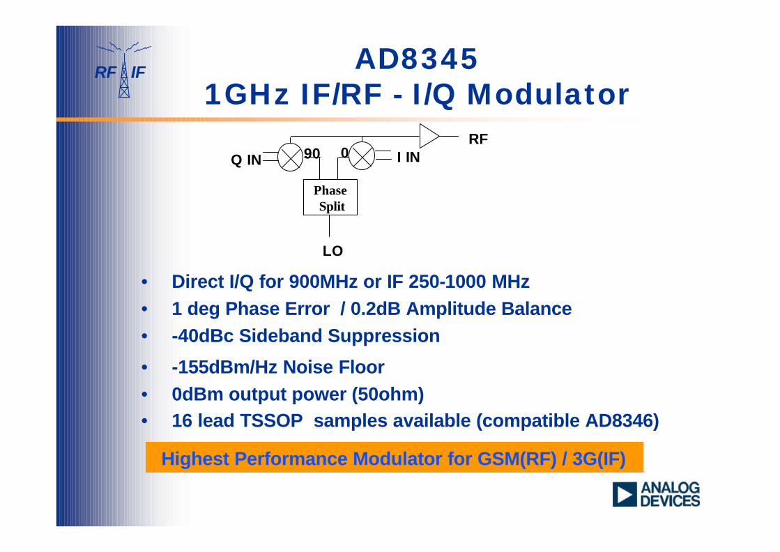
RF IF AD8345 1GHz IF/RF - I/Q Modulator
• Direct I/Q for 900MHz or IF 250-1000 MHz• 1 deg Phase Error / 0.2dB Amplitude Balance • -40dBc Sideband Suppression
• -155dBm/Hz Noise Floor• 0dBm output power (50ohm)• 16 lead TSSOP samples available (compatible AD8346)
Q IN
PhaseSplit
I INRF
90 0
LO
Highest Performance Modulator for GSM(RF) / 3G(IF)
RF IFImage-Rejection W/SSB/LO Calibration for Single or Multi-Carrier Applications
I/Q Single/Multi-Carrier Interleaved or Non- interleaved data
0
090
QuadratureUpconverter
x
x
SAWAD6623 DUC or
QAM ASIC
LPF
LPF
LO4N
Pro
gram
mab
le In
terp
olat
ion
w/F
s/4
or F
s/8
Com
plex
Mod
ulat
ion
14-bit DAC
14-bit DAC
0 FDAC/4
or FDAC/8
0 FDAC/4
or FDAC/8
FLO+FDAC/4
or FDAC/8FLO
FLO/N4M
OSR X FSYMBOL=FLO/(M*N)

RF IF
DIFFERENTIAL“Q”-CH OUTPUT
V-GAIN
90o LO INPUT
EXT LPF
EXT LPF
DIFFERENTIAL“I”-CH OUTPUT
AGC SUB-SYSTEM DETECTOR INPUT
RF INPUT(0.8-2.7GHz)
GAIN CONTROL
AD8347Direct I/Q Demodulator
RF / IF demodulator linear gain control with baseband output amplifiers
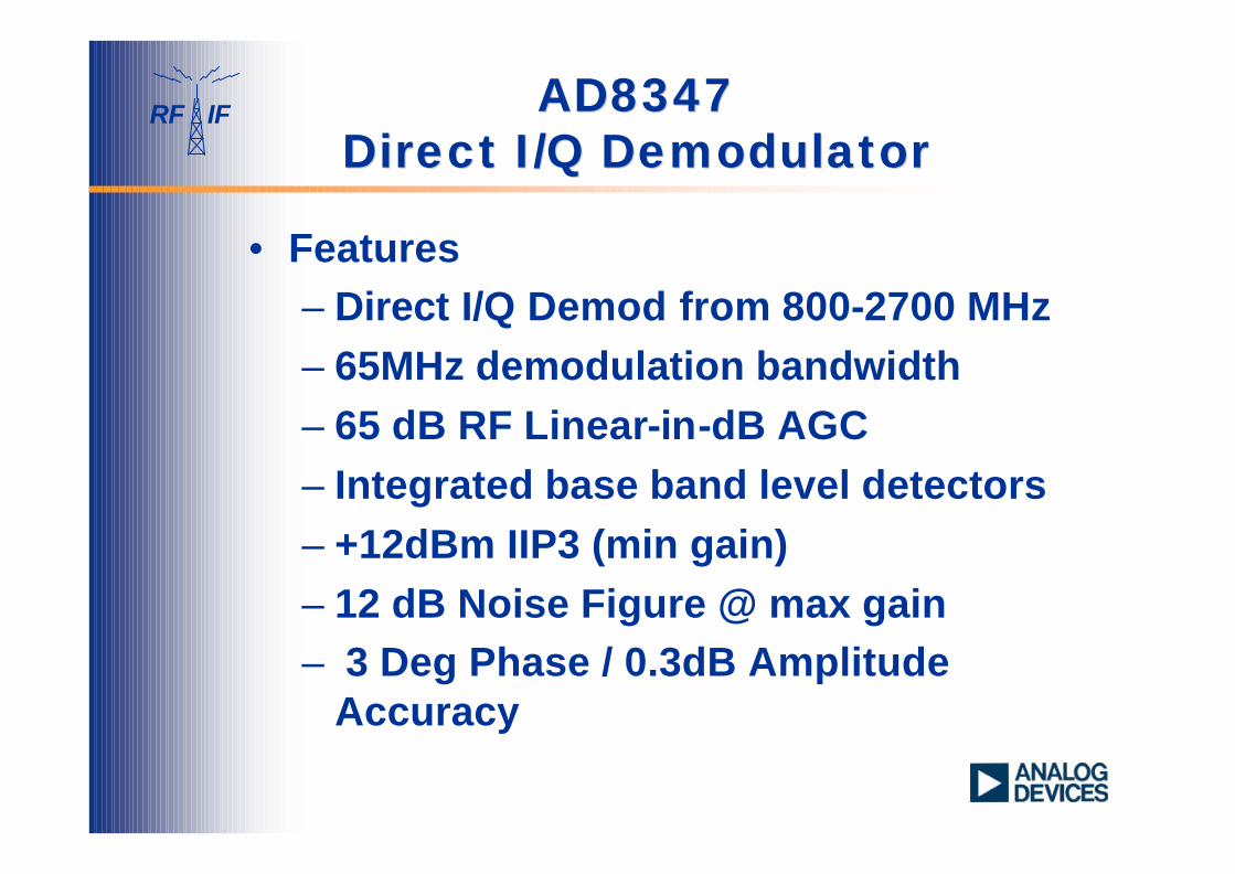
RF IF AD8347AD8347Direct I/Q DemodulatorDirect I/Q Demodulator
• Features– Direct I/Q Demod from 800-2700 MHz – 65MHz demodulation bandwidth– 65 dB RF Linear-in-dB AGC– Integrated base band level detectors– +12dBm IIP3 (min gain)– 12 dB Noise Figure @ max gain– 3 Deg Phase / 0.3dB Amplitude
Accuracy

RF IF
Div/2 0/90o LO Input
EXT LPF
EXT LPF
Differential“I”-Ch Output
Differential“Q”-Ch Output
AGC SUB-SYSTEM Gain ControlInput
RF/IF INPUT50-1000 MHz
AD8348Direct I/Q Demodulator
Gain Control
100-2000 MHz
EXT LPF
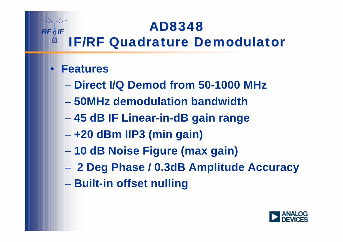
RF IF AD8348AD8348IF/RF Quadrature DemodulatorIF/RF Quadrature Demodulator
• Features– Direct I/Q Demod from 50-1000 MHz – 50MHz demodulation bandwidth– 45 dB IF Linear-in-dB gain range– +20 dBm IIP3 (min gain)– 10 dB Noise Figure (max gain)– 2 Deg Phase / 0.3dB Amplitude Accuracy– Built-in offset nulling
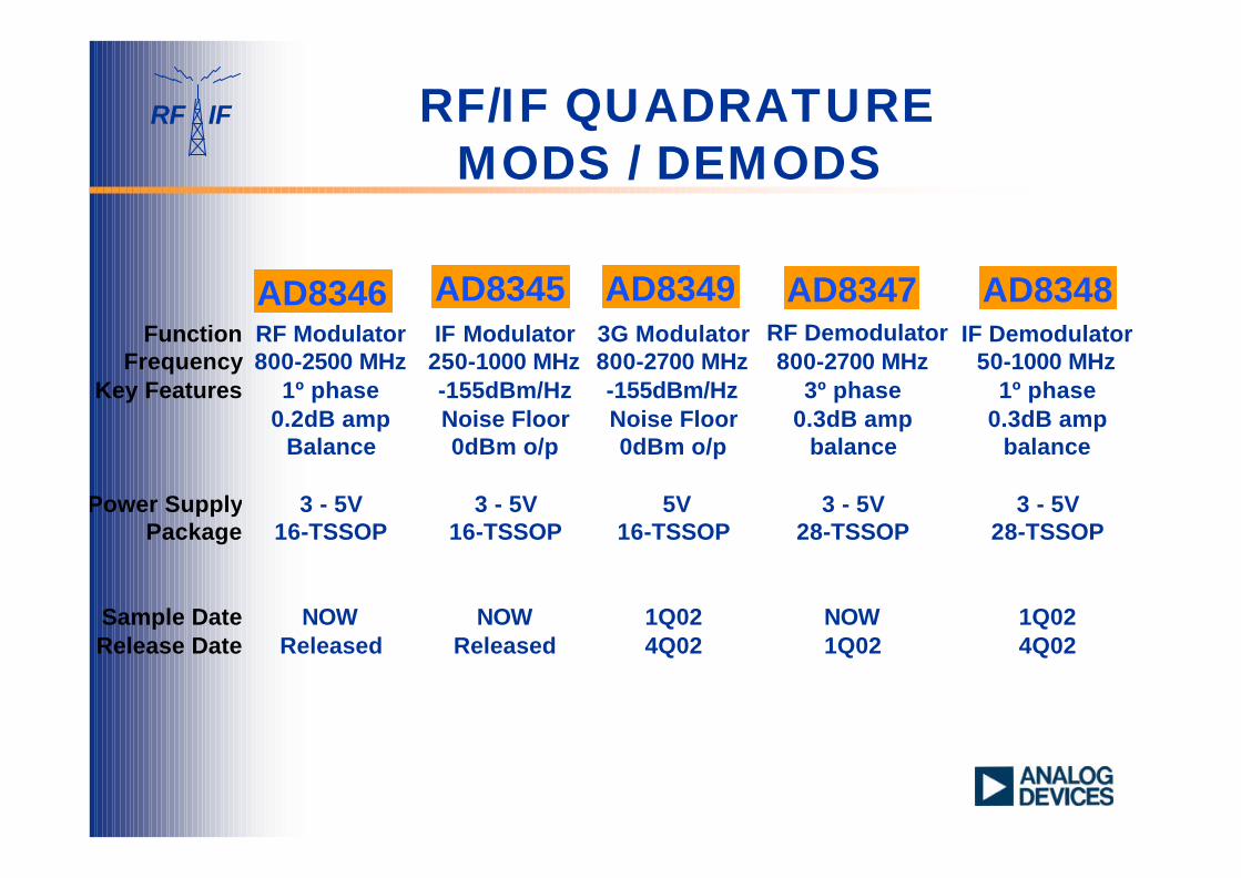
RF IF RF/IF QUADRATUREMODS / DEMODS
FunctionFrequency
Key Features
Power SupplyPackage
Sample DateRelease Date
AD8345 AD8349IF Modulator
250-1000 MHz-155dBm/Hz Noise Floor0dBm o/p
3 - 5V16-TSSOP
NOWReleased
3G Modulator800-2700 MHz-155dBm/HzNoise Floor0dBm o/p
5V16-TSSOP
1Q024Q02
RF Modulator800-2500 MHz
1º phase0.2dB amp
Balance
3 - 5V16-TSSOP
NOWReleased
AD8346IF Demodulator
50-1000 MHz1º phase
0.3dB amp balance
3 - 5V28-TSSOP
1Q024Q02
AD8347 AD8348RF Demodulator800-2700 MHz
3º phase0.3dB amp
balance
3 - 5V28-TSSOP
NOW1Q02
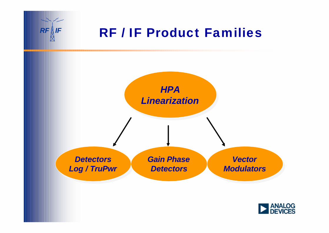
RF IF RF / IF Product Families
DetectorsLog / TruPwr Detectors
Log / TruPwr
HPA Linearization
HPA Linearization
Vector Modulators
Vector Modulators
Gain Phase Detectors
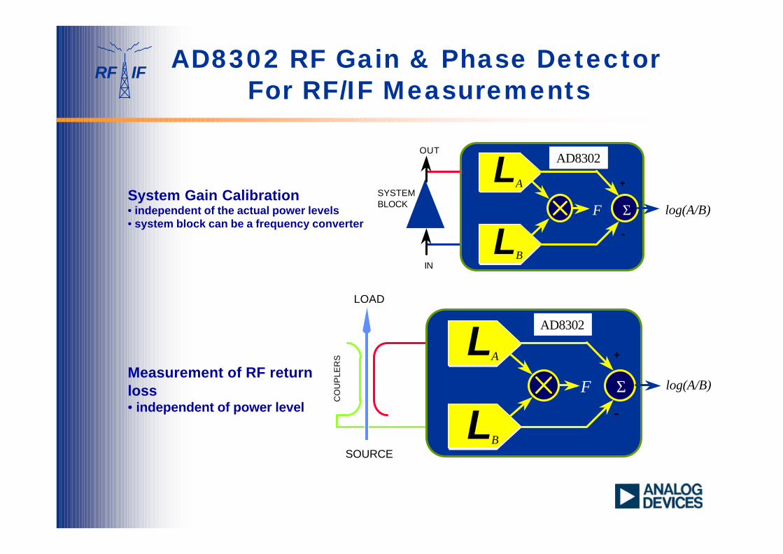
RF IFAD8302 RF Gain & Phase Detector
For RF/IF Measurements
Measurement of RF return loss• independent of power level
log(A/B)
SOURCE
LOAD
CO
UP
LER
S
LA
Σ
+
-
Φ
LB
AD8302
System Gain Calibration• independent of the actual power levels• system block can be a frequency converter
log(A/B)
OUT
IN
SYSTEMBLOCK
LA
Σ
+
-
Φ
LB
AD8302
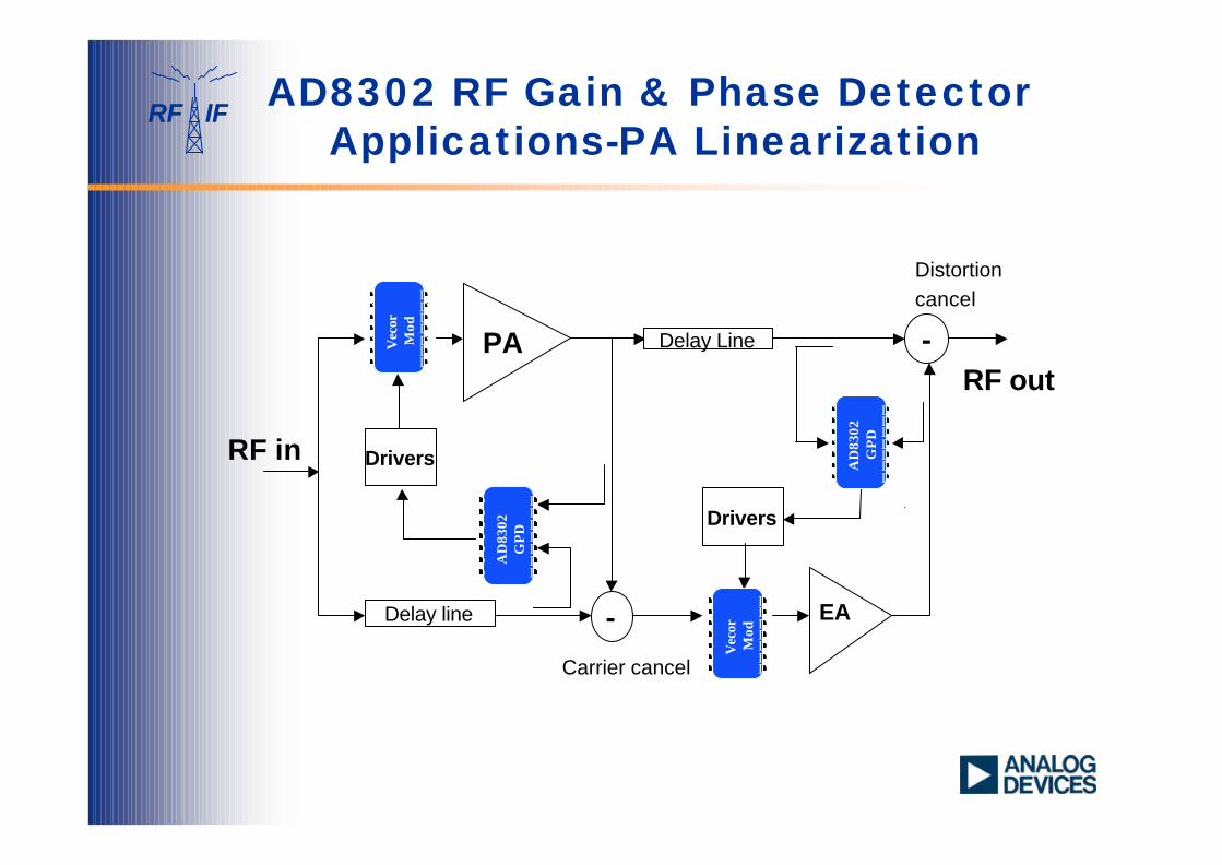
RF IFAD8302 RF Gain & Phase Detector
Applications-PA Linearization
PA
Drivers
-Delay line
-
EA
Delay Line
RF in
RF out
Drivers
Carrier cancel
Distortioncancel
DDDDDDD
DDDDDDD
AD
8302
G
PD
DDDDDDD
DDDDDDD
AD
8302
G
PD
DDDDDDD
DDDDDDD
Vec
orM
od
DDDDDDD
DDDDDDD
Vec
orM
od
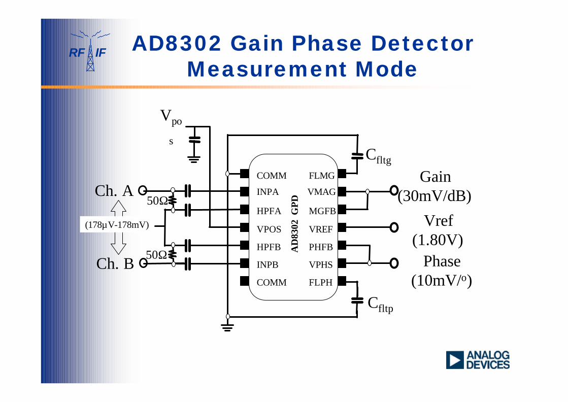
RF IF AD8302 Gain Phase Detector Measurement Mode
D
D
D
D
D
D
D
D
D
D
D
D
D
D
COMM
INPA
HPFA
VPOS
HPFB
INPB
COMM
FLMG
VMAG
MGFB
VREF
PHFB
VPHS
FLPHA
D83
02 G
PD
Ch. A
Ch. B
Vpos
Gain(30mV/dB))
Phase(10mV/o))
Vref(1.80V))
Cfltg
Cfltp
50Ω
(178µV-178mV)
COMM
INPA
HPFA
VPOS
HPFB
INPB
COMM
FLMG
VMAG
MGFB
VREF
PHFB
VPHS
FLPHA
D83
02 G
PD
Vpo
sCfltg
Cfltp
50Ω
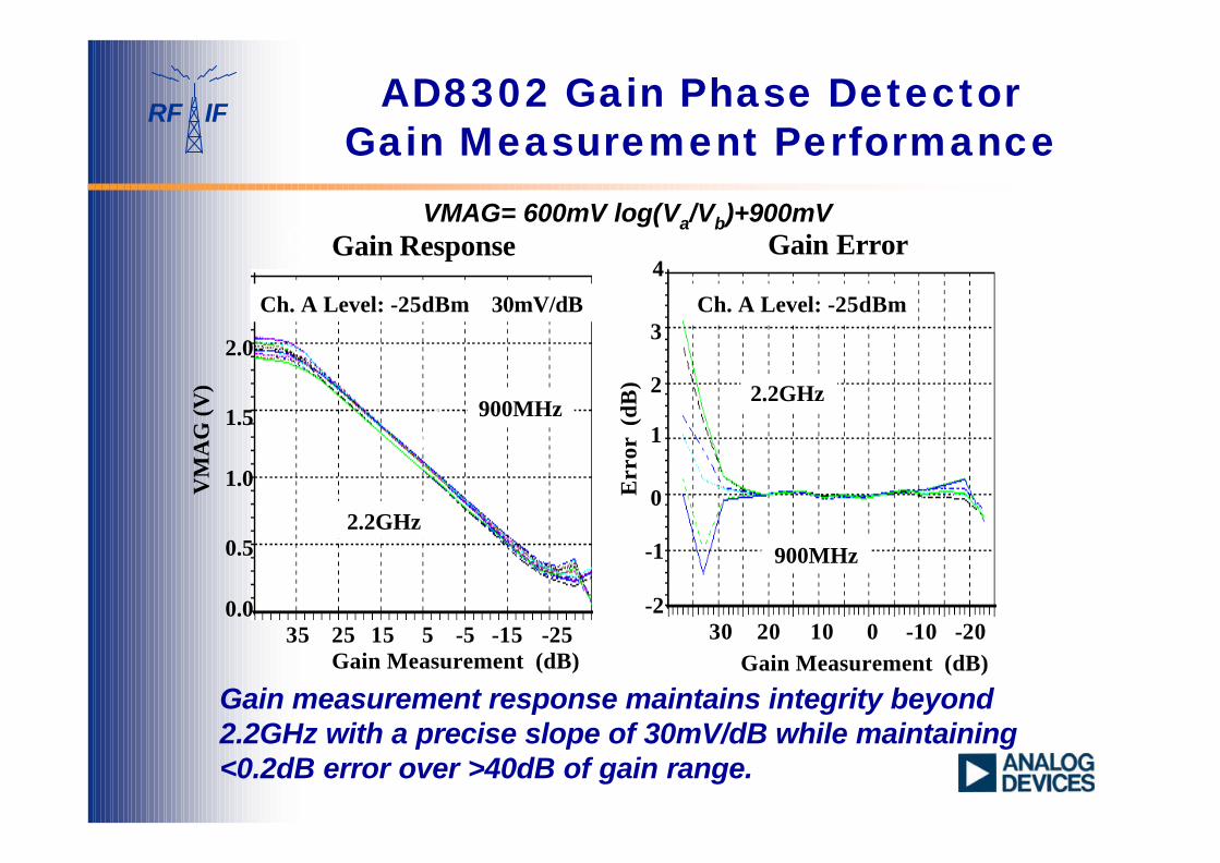
RF IF AD8302 Gain Phase DetectorGain Measurement Performance
Gain measurement response maintains integrity beyond 2.2GHz with a precise slope of 30mV/dB while maintaining <0.2dB error over >40dB of gain range.
Gain Response
30mV/dB
2.2GHz
900MHz
2.0
1.0
0.5
1.5
0.0
VM
AG
(V)
Ch. A Level: -25dBm
Gain Measurement (dB)-25-15-55152535
Gain Error
2.2GHz
900MHz
2
0
-1
1
-2E
rror
(dB
)
Ch. A Level: -25dBm
Gain Measurement (dB)-200
3
4
-10102030
Gain ErrorGain ResponseVMAG= 600mV log(Va/Vb)+900mV

RF IF AD8302 Gain Phase DetectorPhase Measurement Performance
Phase measurement response shows a precise slope of 10mV/deg with a phase error <1 deg over the entire phase range
20
0
-10
10
-20E
rror
(de
g)
30
40Phase Error
Ch. A Level: -25dBm
2.2GHz
900MHz
Phase (degrees)
300200 25015010050 3500
1.80
0.90
0.00
VP
HS
(V)
Phase (degrees) 180 0 1809027090 270 0
Phase Difference Response
10mV/deg
900MHz
2.2GHz
VPHS= 10mV (φa-φb-90o)+900mV