emerging nanophotonics roadmap - csicluxrerum.icmm.csic.es/pdfs/emerging nanophotonics.pdf · 2d...
TRANSCRIPT

Emerging Nanophotonics

Emerging NanophotonicsPhOREMOST Network of Excellence
PhO
RE
MO
ST
Netw
ork of Excellence

�
© �008 PhOREMOST Network of Excellence
All rights reserved. No part of this book may be reproduced in
any form without written permission of the copyright owners.
PhOREMOST Network of Excellence has made all reasonable
efforts to ensure that this roadmap is accurate and up to
date when compiled but accept nor responsibility for errors
or omissions.
Published by PhOREMOST Network of Excellence
Tyndall National Institute
Lee Maltings
Prospect Row
Cork
Ireland
Telephone: +353 �1 490 4075
Rax: +353 �1 490 4435
www.phoremost.org
ISBN 978-0-95597�5-0-8
Design and Layout: Dowling & Dowling Design Consultants LTD
Tel: 0�1 48�1971
Netw
ork of Excellence
PhO
RE
MO
ST

3
Table of ContentsExecutive Summary .............................................................................................................................. 4
Introduction............................................................................................................................................ 6
1. Concepts1.1 Microcavities
Thin-film 1D photonic crystals and Fabry-Perot microcavities ................................................... 102D and 3D optical microcavities .................................................................................................. 16
1.� PlasmonicsSubwavelength surface plasmon optics ...................................................................................... 19
1.3 Non-linear nano-optics
Non-linear nano-optics I .............................................................................................................. ��Non-linear nano-optics II ............................................................................................................. �4Non-linear nano-optics for ultra-sensitive detection ................................................................... �7
1.4 Optical trapping and sortingOptical tweezers .......................................................................................................................... �9
1.5 Metamaterials in the visibleMetamaterials in the visible range ............................................................................................... 3�
1.6 Random LasersPhysics and applications of random lasers ................................................................................. 34
2. Technologies�.1 Infiltration techniques
Opal templating ............................................................................................................................ 38
�.� FunctionalisationFunctionalization for photonic biosensing ................................................................................... 41
�.3 Self AssemblyOpals ........................................................................................................................................... 44Field-assisted self assembly of opals .......................................................................................... 47Assemblies of colloidal quantum dots ......................................................................................... 49Near-infrared colloidal quantum dots for nanophotonics ............................................................ 5�Modelling and optimization in opal-based photonic crystals ...................................................... 55One-dimensional (1D) nanostructures: optical properties .......................................................... 57Colloidal crystals for light manipulation ....................................................................................... 61
�.4 NanofabricationNanoimprinting ............................................................................................................................. 64
�.5 Hybrid TechnologiesFunctional 1-D confined hybrid organic-inorganic nanotechnologies ........................................ 69Heterogeneous integration of III-Vs on silicon ............................................................................. 7�Integration of colloidal photonic crystals ..................................................................................... 74Magnetophotonic crystals ............................................................................................................ 77
3. Emerging Devices�.1 Infiltration techniques
Hybrid organic–nanoparticle solar cells ...................................................................................... 8�Automotive lighting systems ........................................................................................................ 85Nanoparticle-doped organics waveguide optical amplifiers ....................................................... 87Magneto-plasmonics for sensing applications ............................................................................ 90
Technical Acronyms ........................................................................................................................... 92
Contributors ......................................................................................................................................... 93
Subject Index ....................................................................................................................................... 94

4
Executive SummaryNanophotonics is a knowledge area emanating from optics and photonics, which harvest new functions and properties of nanostructures and sub-wavelength phenomena. Its importance for European Research and Development is mainly in the areas of Information and Communication Technologies and fields ICT impacts upon. These encompass the environment, transport, security and life sciences, to name but a few.
The nanometer and molecular scale of materials and phenomena involved offers distinct advantages over existing photonic technologies, such as the prospects of higher integration and, since photons instead of electrons are the main actors, the expectation of less electrical noise. Other aspects will need compromises to be established concerning input signal levels and the extent of energy dissipation in conversion and amplification of signals.
The “Emerging Nanophotonics Roadmap” is an attempt by members of the EU Network of Excellence “Nanophotonics to realise molecular-scale technologies (PhOREMOST)”, an Information and Communication Technologies project, and a few guest scientists, to combine their expertise and views on the way the field is likely to develop over the next 5 to 15 years. It is based on the identification of scientific as well as technological challenges, pointing out roadblocks and suggesting possible strategies to overcome them.
As such this roadmap is likely to be of use mainly to academic and industry-based researchers as well as to research policy actors, in photonics and related application areas. We hope this work will complement other roadmaps, for example the International Technology Roadmap for Semiconductors (ITRS)’ section on Emerging Research Devices and Emerging Research Materials, the Communications Technology Roadmap of the Microphotonics Centre of the Massachusetts Institute of Technology (MIT), the roadmap of the Japanese Optoelectronics Industry and Technology Development Association (OITDA) and the EU project “Merging Photonics and Nanotechnology” (MONA) roadmap.
The figure above illustrates a landscape mapping the maturity status of concepts, technologies, materials and application domains related to nanophotonics covered in this roadmap.
5
As a non-exclusive summary the figure above provides an indication of the maturity of certain technologies of either generic nature or suitable for a family of materials or functions. For example, in the case of visible range metamaterials, much of the concept development research has already been done while the technological challenges remain formidable, suggesting that much technology development in this field is needed.
This edition covers Concepts such as microcavitites, plasmonics, non-linear optical effects in nanostructures, optical trapping and sorting, metamaterials and random lasers. Self-assembly of colloidal structures, nanoimprint lithography as well as functionalisation, infiltration methods and organic-inorganic hybridisation are dealt with under Technologies. A final section on devices addresses nanophotonic developments of photovoltaics, components for the automobile industry, hybrid waveguides and amplifiers as well as plasmonics-based sensors.
This first edition has non-negligible gaps including molecular-scale tuning and switching, DNA-inspired nanofabrication of optical components and systems, novel tools for nano-optics, polymer nanophotonic components and systems, ultra fast cavity switching and quantum information processing, which will be included in future updates. It is planned that a future edition will also look at specific issues such as operating frequency and feature size for a given technology, in the case of the more mature nanophotonics fields.
Taken together, the emerging field of Nanophotonics holds a huge promise of technological and societal benefits envisioned to materialize in the next 5 to �0 years, in which Europe can continue to play a main role.

6
IntroductionThe present document is the first version of emerging nanophotonics roadmap created from the PhOREMOST Network of Excellence (http://www.phoremost.org). It consolidates the effort that has been ongoing during the last two years and that includes, amongst others, coordination meetings with the MONA project (see http://www.ist-mona.org/), internal meetings with the involvement of all PhOREMOST partners, the activities of the PhOREMOST task force on roadmapping, and the inputs from world-level specialists in different fields related to nanophotonics.
This roadmap is focused on emerging concepts and technologies, and thus the focus is on the identification of the main scientific and technological challenges and especially the possible roadblocks. This way, we hope this document will be of special interest to the scientific and technological community in general, acting as an instrument to focus and join forces, working with the common goal of overcoming future limitations. As mentioned above, this effort has been carried out in coordination with the MONA activities, and thus this roadmap should be considered as complementary to their document “A European Roadmap for Photonics and Nanotechnologies”.
Although many of the topics and headlines discussed in this document have components spreading throughout several concepts, technologies and/or devices, we have decided to assign each and every one of them to a main topic within the table of contents skeleton, based on where we believe the centre of gravity belongs. However, we have also included cross-references in the document which point to the related concepts and technologies.
Following this rationale, the document has been organized as follows: in the first part we selected some of the key Concepts that act as building blocks for the emerging nanophotonics activities and which include microcavities, plasmonics, nonlinear optical effects in nanostructures, optical trapping and sorting, metamaterials and random lasers. The second part focuses on Technologies and considers several fundamental technological solutions at the basis of molecular-scale integration; the list includes infiltration techniques, functionalization, self-assembly of opals and colloids, nanoimprint lithography and organic-inorganic hybridization at a molecular scale. Finally, the third part of the document focuses on some emerging devices and applications. The potential application domains considered are consistent with those of the Strategic Research Agenda of the European Technology Platform Photonics�1 (http://www.photonics�1.org).
The number of topics covered by the roadmap is necessarily limited and cannot be considered complete. We have made an effort to produce a document with a broad scope which we believe will be useful to a large audience, gathering inputs from specialists both within and outside PhOREMOST. However, the list of topics is expected to grow in the future. This should be considered as a living document, which will be revised and improved throughout the lifetime of the PhOREMOST network of excellence and beyond, adding additional topics whenever it becomes appropriate and letting others disappear as they may lose relevance.
All entries in the document have been generated with a common template that includes the following headlines:
Potential application domains: list of the relevant areas of the Photonics�1 Strategic Research Agenda
Free-text keywords
Cross references to other sections of the document (clickable on the electronic version)
Date of issue, institution and author’s name
Context
Motivation
Key performance figures, including state-of-the-art figures and references
Activity in the field and evolution
Main scientific and technical challenges. This section has been color coded, indicating the degree of difficulty for achieving the challenges: Red (No known solutions at this time), Yellow (Very hard but possible solutions), Green (feasible solutions under investigation), White (known solutions, first commercial products available)
•
•
•
•
•
•
•
•
•

7
Timeline: This section shows the expected evolution over time for the different scientific and technical challenges above.
Dependencies: identification of the main scientific and technological developments needed to ensure success.
Conclusions and recommendations.
PhOREMOST Roadmap TaskforceGonçal Badenes, ICFO (Chairman)
Alfonso Cebollada, IMM-CSIC
Nikolai Gaponik, TU-Dresden
Cefe Lopez, ICMM-CSIC
Mary Claire O’Regan, Tyndall
Davide Piccinin, Corecom
Silvia M. Pietralunga, Corecom
Diederik Wiersma, LENS
Clivia Sotomayor Torres, ICN
DISCLAIMER: This document represents the views of the authors of the different sections. Although the data presented is correct and accurate to the best of our knowledge at the time of publication, we do not make any representations or warranties about the accuracy, completeness or timelines of the information presented, whether express or implied, in this document. This roadmap is devised and intended for scientific and technological assessment only and is without regard to
•
•
•

8

01Concepts

10
1. Concepts1.1 MicrocavitiesThin-film 1D photonic crystals and Fabry-Perot microcavities
Potential application domains:
Information and Communication
Lighting and Displays
Security, Metrology and Sensors
–
–
–
Free-text keywords: thin-film, multilayer, one-dimensional photonic crystal, Fabry-Perot microcavity, resonant cavity light-emitting diode (RCLED), vertical cavity surface emitting laser (VCSEL), resonant-cavity-enhanced photodetector, microcavity polariton, distributed Bragg reflector (DBR), omnidirectional mirror
Cross-references to other sections of document:
�D and 3D optical microcavities
Date of Issue: 09/06/07 Institution and author’s name: Alexander Dukin, Ioffe SP
Context:
Planar microcavities with distributed Bragg reflectors (DBRs) were probably one of the first examples of spatial confinement of light in the solid state. Planar microcavities are an excellent field for testing new concepts and ideas, which would be realized later in �D and 3D structures and have allowed the study of effects predicted by cavity quantum electrodynamics: strong and weak coupling between a quantized photon and electron, an enhancement and suppression of spontaneous , anomalous Lamb shift, Rabi oscillations and splitting, a generation of non-classic light and so on in solid-state environment [1]. Microcavities in 1D photonic crystals possess some valuable device-relevant properties: they enable a high value of dielectric indices ratio [�], incorporate semiconductor quantum wells and quantum dots (QDs) in a cavity and they can serve as a base for preparation of 3D photonic crystals [3] and photonic dots or “molecules” [4]. From the device point of view thin-film 1D photonic crystals and Fabry-Perot microcavities were the base for vertical-cavity surface-emitting lasers (VCSELs) [5-7], resonant-cavity light-emitting diodes (RCLEDs) [8-11], resonant-cavity-enhanced photodetectors [1�-14], omnidirectional dielectric mirrors [15, 16] and electro-optic modulators [6]. Moreover, they are also very promising for single-photon sources [17] and for quantum information processing. Furthermore, simple thin-film multilayer stacks can also serve as photonic quasicrystals and fractal structures, which possess peculiar photonic properties [18]. An inclusion of magneto-optical effects is expected to lead to more sophisticated and complex physics and devices such as optical isolators [19]. Recently, it was predicted that simple one-dimensional transparent metallodielectric stacks can possess the properties of left-handed metamaterials: all-angle negative refraction for propagating waves, as well as evanescent wave amplification and sub-wavelength focusing [�0, �1]. Another important direction is the study of collective coherence in planar semiconductor microcavities, such as Bose-Einstein condensation of microcavity polaritons [��, �3] and polariton lasing [�4-�8]. These macroscopic phase coherence phenomena open the way to new horizons of quantum physics and light-matter interaction.

11
Motivation:
1D photonic crystals can be easily fabricated and modelled unlike 3D photonic structures. They possess valuable optical properties that can be applied in many optical devices. They can help to a better understanding of the fundamental physics in some new fields.
The fields of technical interest include: near-ultraviolet solid-state lasers, mid-infrared solid-state lasers, RCLEDs and VCSELs for optical fibre telecommunication, high brightness organic Light Emitting Diodes (LEDs) for flexible displays, RCLEDs for sensors, printers, and scanners, single-photon sources, cavity-enhanced selective photodetectors that allow DWDM, electro-optic modulators, omnidirectional dielectric lossless mirrors, optical isolators, microcavity exciton-polariton devices: polariton lasers, spin transistors, polarization modulators, optical switches, and spin-memory elements.
The fields of scientific interest include: Bose-Einstein condensation of microcavity polaritons, polariton lasing and superfluidity, generation of non-classic light, quantum coherence at elevated temperatures, static and dynamical optical processes at the photonic band edge, the properties of the one-dimensional left-handed metamaterials: all-angle negative refraction for propagating waves, sub-wavelength focusing and evanescent wave amplification, the optical properties of photonic quasicrystals and fractals.
The fields of quantum information technologies. Strong coupling regime between a single quantum emitter (QD) and a cavity mode is of great interest for a variety of quantum information applications, especially with a solid-state implementation. A strong coupling QD-microcavity system could lead to nearly-ideal single-photon sources for quantum information processing (e.g. for quantum cryptography), with extremely high efficiency and photon indistinguishability. The same technology could be applied as an interface between a spin qubit and single-photon qubit in a quantum network.
–
–
–
–
Key performance figures:
For microcavities: quality factor (Q) of microcavity = 1730 [17], finesse of microcavity, wavelength of a mode, spontaneous emission coupling factor of a mode, mode angular width, Purcell factor = 147 [1].
For VCSELs: threshold current density, internal quantum efficiency, wall-plug efficiency of 30% [6], differential efficiency = 0.71 W/A [7], modulation speed >20 Gbit/s [6], beam divergence, brightness, output optical power = 10 mW (cw) [6].
For RCLEDs: brightness, modulation bandwidth = 200 MHz [9], output optical power = 15 mW (cw) [9], external quantum efficiency = 23% [11], transmission rate = 622 Mbit/s [9].
For electro-optic modulator: modulation frequency ~35 GHz [6].
For 1D photonic crystals: refractive indices ratio ~3.5 [2], relative stop-band width = 0.75% [2], reflection coefficient.
For microcavity polaritons: value of vacuum Rabi splitting = 80 meV [23], temperature of Bose-Einstein condensation = 300 K [28], effective mass =(2.6x10⁻⁵ of the vacuum electron mass [27], laser emission threshold =1 mW [28].0
For 1D left-handed metamaterials: object-lens and object-image distances, image resolution, the values of negative permeability, negative permittivity, negative refractive index, and negative refraction angle, the wavelength range of negative index.
–
–
–
–
–
–
–
Activity in the field: high Dynamics: expanding

1�
References:
[1] K.J. Vahala, Nature 4�4, 839 (�003).
[�] T. Schwarzl, et al. J. Appl. Phys. 101, 09310� (�007).
[3] E. Pavarini et al. Phys. Rev. E 66, 03660� (�00�).
[4] M. Bayer, et al. Phys. Stat. Sol. (a) 191, 3 (�00�).
[5] “Vertical-Cavity Surface-Emitting Lasers”, MRS Bulletin �7, (�00�) and articles therein.
[6] N.N. Ledentsov, et al. Proc. IEEE 95, 1741 (�007).
[7] F. Hopfer, et al. IEEE Sel. Topics Quant. Electronics 13, 130� (�007).
[8] D. Delbeke, et al. IEEE J. Sel. Topics Quant. Electron. 8, 189 (�00�).
[9] M. Pessa, et al. Semicond. Sci. Techn. 17, R1 (�00�).
[10] P.H. Lei, et al. Sol. State Electron. 5�, ��7 (�008).
[11] R. Joray, et al. IEEE Phot. Technolog. Lett. 18, 105� (�006).
[1�] Q. Han, et al. Appl. Phys. Lett. 89, 131104 (�006).
[13] H. Zogg, et al. Infrared Phys. & Techn. 49, 183 (�007).
[14] A. Ramam, et al. Appl. Phys. Lett. 86, 171104 (�005).
[15] A.G. Barriuso et al. Appl. Opt. 46, �903 (�007).
[16] N. Krumbholz et al. Appl. Phys. Lett. 88, �0�905 (�006).
[17] D. Press, et al. Phys. Rev. Lett. 98, 11740� (�007).
[18] W. Steurer et al. J. Phys. D 40, R��9 (�007).
[19] Z. Yu, et al. Appl. Phys. Lett. 90, 1�1133 (�007).
[�0] M. Scalora, et al. Opt. Expr. 15, 508 (�007).
[�1] H. Shina, et al. Appl. Phys. Lett. 89, 15110� (�006).
[��] R. Balili, Science 316, 1007 (�007).
[�3] P. Littlewood, Science 316, 989 (�007).
[�4] A. Kavokin, et al. Phys. Lett. A 306, 187 (�003).
[�5] A. Kavokin, Appl. Phys. A 89, �41 (�007).
[�6] L.V. Butov, Nature 447, 540 (�007).
[�7] J. Keeling, et al. Semicond. Sci. Techn. ��, R1 (�007).
[�8] S. Christopoulos, et al. Phys. Rev. Lett. 98, 1�6405 (�007).

13
Main scientific and technical challenges to be addressed:
Increase of the lateral confinement of an optical field in a planar microcavity and suppression of radiation leakage into waveguide and whispering gallery modes. This requires a special design of the cavity layer and the lateral geometry of the cavity.
Increase of the conductivity and a reduction of the heat resistance of DBRs, in order to obtain an electrical excitation of luminescence and provide an efficient thermal power dissipation. This requires: a reduction of the DBR series resistance using sophisticated heterointerface designs and doping profiles, intracavity metal contacts, innovative current injection schemes and architectures, air cooling of lasers in post geometry.
Increase of the weak absorption of an optical excitation energy in the active layer of a planar microcavity. This requires novel schemes of optical excitation, e.g. via a microcavity eigenmode.
Selection of semiconductor and dielectric compounds and development of a technology for the epitaxial growth of lattice-matched Bragg reflectors and gain regions in the desirable wavelength ranges: from blue and near-ultraviolet up to telecommunication wavelengths (1.3 and 1.55 µm) and mid-infrared. This requires: a separate growth of DBRs and active regions, and then wafer-bonding of the different materials together, a selection of the materials suitable for the epitaxial growth of all VCSEL layers, the pseudomorphological growth of active regions, with the substrate’s lattice constant instead of their own.
Realization of compact broadband optical isolators. Requires a growth technology of multilayer structures including magnetic and dielectric materials.
Realization of a polariton laser at room temperature. Requires new materials with a high exciton binding energy and exciton–photon interaction strength.
Realization of the on-demand single-photon sources. Requires a coherent pump scheme, such as the involvement of a cavity-assisted spin flip Raman transition.
Realization of the “perfect lens” in the visible range using 1D multilayer structure to achieve super-resolution below the diffraction limit. Requires: overcoming the inherently large absorption and scattering losses of metal layers and a fabrication technique of multilayer stacks composed of very thin metal and dielectric layers.

14
Timeline:
� – 5 years 5 – 10 years 10 years and more
Lateral confinement and radiation leakage of planar microcavity
Conductivity and heat resistance of DBRs
Optical energy absorption of planar microcavity
Materials and technology for the epitaxial growth of Bragg reflectors and gain regions.
Realization of compact broadband optical isolators
Realization of the polariton laser at room temperature
Realization of the on-demand single-photon sources
Realization of the “perfect lens” by 1D multilayer structure
Dependencies:
Growth technologies of new compounds: lattice-matched optically transparent heteropairs with a high contrast of refractive indices in the desired wavelength range.
Thin film deposition techniques: CVD, plasma-enhanced CVD, metal-organic CVD, molecular-beam epitaxy, vapor-phase epitaxy, metal-organic vapor-phase epitaxy, atomic layer depositon, magnetron sputtering, pulsed laser deposition, cathodic arc deposition, ion beam (sputter) deposition, sol-gel technology, spin coating etc.
High-precision in-situ control of a thickness and composition of grown films.
Etching techniques for post etching and lateral patterning: ion etching, sputter etching, vapor phase etching, liquid-phase etching, chemical etching, electrochemical etching, photochemical etching, etc.
Doping techniques: ion implantation, magnetron sputtering, metal-organic chemical vapor deposition etc.
Growth and self-organisation of quantum-confined structures: quantum wells, quantum wires and quantum dots inside a structure.
Theoretical models: transfer matrix method, scattering matrix method, Green functions of sources in a planar multilayer and post-like structures.
–
–
–
–
–
–
–

15
Conclusions and recommendations:
In spite of its relative simplicity, 1D photonic crystals and microcavities have promising perspectives and significant potential for further development. In order to remain on the leading edge of the science and technology there is a strong need in serious efforts on the further development of both solid-state technology and theoretical models.
Areas to be initiated:
The study of propagation of short light pulses in 1D structures
The study of optical properties of magneto-dielectric and metal-dielectric structures
The investigation of microcavities and 1D photonic crystals based on new material systems such as polymers etc.
The study of the interaction between plasmonic resonances in metallic nanostructures and a confined optical mode in microcavities
The design of photonic structures that simultaneously break time-reversal, spatial inversion, and mirror symmetries, and the study of their photonic properties
Areas to be abandoned: none
Dependencies: technologies of thin film deposition, epitaxial growth, active media formation, selective etching and doping, high-precision control of layers.
Due to the wide diversity of one-dimensional photonics, it will be better to choose most perspective directions and concentrate efforts on the most promising from the device point of view or having the largest potential for future technological breakthrough.
•
•
•
•
•
16
2D and 3D optical microcavities
Potential application domains:
Information and Communication
Life Sciences and Health
Lighting and Displays
Security, Metrology and Sensors
–
–
–
–
Free-text keywords: Microcavity, microresonator, Fabry-Perot, whispering gallery mode, morphology dependent resonance, optical mode, quality factor, free spectral range, mode volume
Cross-references to other sections of document:
Thin-film 1D photonic crystals and Fabry-Perot microcavitiesNon-linear nano-optics for ultra-sensitive detectionMetamaterials in the visible rangePhysics and applications of random lasersOpals
Date of Issue: �8/03/�008 Partner: Ali Serpengüzel, Koç University, Istanbul, Turkey
Context:
Optical microcavities covered in this section include microspheres (3D), microspheroids (3D), microtoroids (3D), microdisks (�D), microrings (�D), microracetrack (�D), microspiral (�D) and micropolygon (�D). These microcavities can be formed from a high index material inside a low index material (e.g., air) or can be an intentional defect inside a more complex ordered or disordered (random) photonic microstructure. These ordered complementary microstructures are photonic crystals or photonic bandgap materials, metamaterials and the disordered complimentary microstructures are the optical glasses. There is a bottom up approach, where microcavities are assembled into larger photonic structures. There is also a top down approach, where microcavities are formed inside larger photonic structures as “defects.” The “defect” microcavities inside photonic crystals as well as Fabry-Perot (1D) microcavities will not be covered in this section.
Motivation:
High intensity optical fields: The atomic and condensed matter physics communities approach these optical microstructures with scientific and basic research interest. For physicists, the main interest in these optical microstructures is for their ability to sustain high optical fields and therefore strongly interact with the material with which the optical microresonator is constructed from.
High quality factor optical modes: The optoelectronics community however has a purely technological interest and approaches these optical resonators with an applied research interest. The optical communication engineers would like to manufacture high quality devices such as filters, light sources, detectors, attenuators, modulators, switches, or wavelength converters for dense wavelength division multiplexing applications in optical fiber communication or sensors for remote sensing.
–
–
17
Key performance figures:
High Q microspheres in air (dielectric) [1], semiconductor) [2],
High Q microspheres 1D chain [3], 2D array [4], 3D lattice [5],
High Q microtoroids in air [6], 1D chain [7],
High Q microspiral in air [8], 1D chain [9],
High Q micropolygon in air[10],
High Q microrings in air[11], 1D chain[12], 2D array[13],
High Q microdisks in air[14], 1D chain[15], 2D array [16].
–
–
–
–
–
–
–
Activity in the fiel: High Dynamics: Expanding
References:
[1] Rayleigh scattering in high-Q microspheres, ML Gorodetsky at al , JOSA B, Vol. 17, 1051 (�000).
[�] Optical Channel Dropping with a Silicon Microsphere, YO Yilmaz et al, IEEE Photon. Technol. Lett. 17, 166� (�005).
[3] Band Formation in Coupled-Resonator Slow-Wave Structures, BM Möller et al Opt. Express, 15, 1736� (�007).
[4] Optical coupling and transport phenomena in chains of spherical dielectric microresonators with size disorder, VN Astratov et al Appl. Phys. Lett. 85, 5508 (�004).
[5] Percolation of light through whispering gallery modes in 3D lattices of coupled microspheres, VN Astratov, Opt. Express 15, 17351 (�007).
[6] Ultrahigh-Q toroidal microresonators for cavity quantum electrodynamics, SM Spillane et al Phys. Rev. A 71, 013817 (�005).
[7] Free ultra-high-Q microtoroid: a tool for designing photonic devices, M Hossein-Zadeh et al, Opt. Express 15, 166 (�007).
[8] Current-injection spiral-shaped microcavity disk laser diodes with unidirectional emission, M Kneissl et al Appl. Phys. Lett. 84, �485 (�004).
[9] High-Q-preserving coupling between a spiral and a semicircle µ-cavity, GD Chern et al, Opt. Lett. 3�, 1093 (�007).
[10] Waveguide-coupled octagonal microdisk channel add-drop filters, C Li et al, Opt. Lett. �9, 471 (�004).
[11] Ultrahigh-quality-factor silicon-on-insulator microring resonator, J Niehusmann, et al, Opt. Lett. �9, �861 (�004).
[1�] Very high-order microring resonator filters for WDM applications, BE Little, et al, IEEE Photon. Technol. Lett., 16, ��63 (�004).
[13] Microring resonator arrays for VLSI photonics, BE Little et al, IEEE Photon. Technol. Lett., 1�, 3�3 (�000).
[14] Self-induced optical modulation of the transmission through a high-Q silicon microdisk resonator, TJ Johnson et al, Opt. Express 14, 817 (�006).
[15] Photonic molecule laser composed of GaInAsP microdisks, A. Nakagawa, et al Appl. Phys. Lett. 86, 04111� (�005).
[16] An optical fiber-taper probe for wafer-scale microphotonic device characterization, CP Michael et al, Opt. Express, 15, 4745 (�007).

18
Main scientific and technical challenges to be addressed:
Optical coupling to microresonators: optical fiber couplers, tapered optical fibers, SOI waveguides are used. Solved for microdisks, microrings, can be solved in principle for micropolygons, but remains to be solved for microspheres and microtoroids.
Light generation in semiconductor resonators:solved in III-V photonics, but remains to be solved in silicon photonics
Integration in the vertical dimension: solved for microdisks and microrings, can be solved in principle for micropolygons but remains to be solved for microspheres, microtoroids.
Timeline:
� – 5 years 5 – 10 years 10 years and more
Optical coupling to cicroresonators:
Light generation in semiconductor resonators:
Integration in the vertical dimension:
Dependencies:
High Q microcavities: optical coupling, chemistry–
Conclusions and recommendations:
High quality factor (Q) optical microcavity research is a rapidly growing field. Many research groups are coming into the field. Optical microcavities are addressed with optical waveguides. Coupling is performed either from cavity to cavity or by optical waveguides. Microring-based optical chips are already in the market. Micropolygons can effectively compete with the microrings. Microdisks need a niche market. Microtoroids have very high quality factors but optical connectivity remains to be solved. Microspheres can be integrated into the vertical dimension again with optical interconnectivity to be solved. Microspirals are novel structures, which break the clockwise and counterclockwise symmetry of the other microresonators and therefore have a directional optical output.

19
1.2 PlasmonicsSubwavelength surface plasmon optics
Potential application domains:
Information and Communication
Life Sciences and Health
Lighting and Displays
Security, Metrology and Sensors
–
–
–
–
Free-text keywords: High sensitivity bio-chemical sensing, miniaturized interconnects, enhanced spectroscopy.
Cross-references to other sections of document:
Non-linear nano-optics IIOptical tweezersFunctionalization for photonic biosensingNanoimprintingMagneto-plasmonics for sensing applications
Date of Issue: �0/06/07 Partner: Romain Quidant, ICFO
Context:
Plasmon optics which uses surface plasmons (SP) supported by metal nanostructures has recently shown to be one of the most promising approaches to overcome diffraction and extend optics down to the nanometer scale. While the last five years have seen huge advances in the understanding and the applications of SP, several key challenges remain still to be demonstrated to evaluate their actual contribution in the elaboration of future nanophotonic devices.
Motivation:
Enhanced light-matter interaction at the nanoscale: Efficient optical addressing of single nano-objects down to the molecular level would have crucial impact on enhanced spectroscopy, bio-imaging, enhanced optical forces, high harmonic generation (SHG, THG). Furthermore, by combining subwavelength mode confinement with sharp spectroscopic features the sensitivity of SP-based bio-chemical sensors is expected to be strongly improved.
Plasmons routing at the sub-micrometer scale for short distance interconnects: The main challenge is to maintain significant propagation distances while squeezing transversally the mode to subwavelength sections. This would contribute to dramatically scale down integrated optical and opto-electronical devices.
New hybrid materials: By mixing metals with other organic and inorganic materials (i.e. semi-conductors, polymers, magnetic materials, …) to achieve composites with novel optical properties. There is a special interest for hybrid plasmonic materials with properties than can be controlled by an external stimulus (by light, electric and magnetic fields, etc …).
–
–
–

�0
Key performance figures:
Molecular sensitivity in Surface Enhanced Raman Scattering (SERS) [1]
Femtomolar sensitive bio-chemical sensors [3,4]
Light guiding through submicrometer sections down to 100 nm section [5-7]
SP-enhanced optical forces with an enhancement factor of several orders of magnitude, parallel and selective trapping at a surface[8-10]
–
–
–
–
Activity in the field: High Dynamics: Expanding
References:
[1] Walter et al, Phys. Rev. Lett. 98, 137401 (�007)
[�] Anger et al, Phys. Rev. Lett. 96, 11300� (�006)
[3] Raschke et al, NanoLett. 3, 935 (�003)
[4] MacFarland et al, NanoLett. 3, 1057 (�003)
[5] Bozhevolnyi et al, Nature 440, 509 (�006)
[6] Krenn et al, Phys. Rev. Lett. 95, �57403 (�005)
[7] Dionne et al, NanoLett. 6, 19�8 (�007)
[8] Volpe et al, Phys. Rev. Lett. 96, �38101(�006)
[9] Righini et al, Nature Phys 3, 477 (�007)
[10] Svedberg et al, NanoLett. 6, �639 (�006)
Main scientific and technical challenges to be addressed:
Field confinement below the �0 nm level: Requires improving geometrical control of SP nanostructures with a nano-resolution (shape, edge, surface roughness, separation distances, …).
Field Enhancement factor above 100: Requires improving geometrical control and minimizing defects. Dissipation in lithographically prepared samples is a limiting factor that can be significantly reduced by using crystalline metals.
SP guiding through sections smaller than 100 nm: Requires mode engineering combining transverse confinement with low penetration within the metal.
Controlling the dynamics of single molecules: Would require new methods to locate the molecule at the right position relatively to the metal structures (both at the hot-spot location but also at a controlled distance from the metal surface to limit quenching).
Trapping objects as small as 100 nm: A major issue at this scale is the strong Brownian motion which needs to be compensated by strong subwavelength traps with dimensions commensurable with the object size.

�1
Timeline:
� – 5 years 5 – 10 years 10 years and more
Field confinement below the �0 nm level
Field Enhancement factor above 100
SP guiding through sections smaller than 100 nm
Controlling the dynamics of single molecules
Trapping objects as small as 100 nm
Dependencies:
Enhanced spectroscopy: Chemistry, lithography
SP-based sensing: Chemistry, engineering of the mode volume
SP routing: side-wall roughness, gold crystallinity
SP-enhanced forces: microfluidics, lithography, chemistry
–
–
–
–
Conclusions and recommendations:
Plasmonic nano-optics is a rapidly expanding, broad field with many potential applications. Many research groups have recognised this potential and have started or increased their activities in the field. Although some initial applications are finding their way to commercialisation (e.g. surface-plasmon resonance sensors), the need for basic understanding of the physics – especially at the nanoscale – and for the development of new techniques, concepts and methods is key for the real exploitation of the full potential of plasmonics, and will undoubtedly lead to the appearance of ground-breaking devices in the next decades. In order for this to happen, it is still necessary to narrow down the large array of possible application domains to the ones where real, competitive applications can arise. This process will certainly lead to the dismissal of some of the proposed schemes, but even in those cases, a large amount of scientific and technical knowledge will be generated.

��
1.3 Non-linear nano-opticsNon-linear nano-optics I
Potential application domains:
Information and Communication
Security, Metrology and Sensors
–
–
Free-text keywords: Quantum light generation, quantum computing, quantum information
Cross-references to other sections of document:
Non-linear nano-optics IINon-linear nano-optics for ultra-sensitive detectionMetamaterials in the visible rangeOpalsIntegration of colloidal photonic crystals
Date of Issue: �7/03/�008 Institution and author’s name: C. Sibilia , UR-DE
Context:
Harmonic and nonlinear photon generation in nano-structured materials can be exploited in perspective for quantum information and quantum computing
Motivation:
Sources – Sources able to generate photons pairs in the visible remain an appealing resource for practical quantum information processors since they interact very little with the environment, propagate easily over long distances, and are important for quantum metrology (e.g. to improve the measurement accuracy: as in quantum interferometry, quantum ellipsometry, etc.), as well as in the promising new field of quantum lithography. Photonic Crystal Structures (PhCs) are a tool to develop new miniaturized and integrable parametric oscillator sources, as well as narrow band and efficient sources of correlated photons, in the broad wavelength range from the near infrared down into the ultraviolet, covered by using second-order parametric frequency conversion or third-order nonlinear interactions. The large bandgap group-III Nitride semiconductors (such as GaN, AlN and AlGaN) have had a massive impact on photonics and optoelectronics in the last decade however the nonlinear optical response of nano-/micro-dimension structures in such material systems remains to be explored properly, but the time is now ripe for such developments to be undertaken, with the potential for significant enhancements and radical extension of the functionality range available.
Signal Detection 1.5µm single-photon detector based on the principle of frequency. Up- conversion based on nonlinear nanostructures. Miniaturized nonlinear frequency up converters could enable a continuous and fast measurement with a simple and practical control system without the requirement of gate trains or post-signal-processing algorithms.
–
–
Key performance figures:
The top efficiency sources of correlated photons emitting 106 s-1 photons in the IR was reported in photonic crystal fibres for several meters of fibre length [1].
Efficient up conversion single photon detection reported in ref. [2]
–
–
Activity in the field: Medium Dynamics: Expanding

�3
References:
[1] J. G. Rarity, J. Fulconis, J. Duligall, W. J. Wadsworth, P. St. J. Russell. “Photonic crystal fiber source of correlated photon pairs” Optics Express 13, 534 (�005)
[�] E. Diamanti, C. Langrock, M. M. Fejer, Y. Yamamoto, H. Takesue ” 1.5µm photon-counting optical time-domain reflectometry with a single-photon detector based on upconversion in a periodically poled lithium niobate waveguide. Opt.Lett 31, 7�7 (�006)
Main scientific and technical challenges to be addressed:
Losses due to surface defects and/or roughness arising from fabrication processes could strongly reduce the efficiency of the wavelength conversion processes, preventing the generation of entangled photons
The low value of the second order nonlinearity will require a strong light localization in order to obtain sufficient enough efficiency.
Technology issue to be adopted as a function of the sample structure and morphology.
Timeline:
� – 5 years 5 – 10 years 10 years and more
Surface defects
Low value of the second order nl
Technology issue
Dependencies:
Theory of nonlinear propagation,
growth techniques
etching technology
–
–
–
Conclusions and recommendations:
The implementation of sources based on correlated photons requires cross-disciplinary skills covering a formidable range of expertise in epitaxial growth, nano and micro-technology, photonic crystal science, non-linear optics, theoretical and computational modelling techniques, quantum optics and source characterisation, materials evaluation and structure.

�4
Non-linear nano-optics II
Potential application domains:
Design and Manufacturing of Components and Systems–
Free-text keywords: integrated planar devices, harmonic signal generation, parametric processing, signal propagation and multiplexing, enhanced sensitivity detection for bio-sensing
Cross-references to other sections of document:
Subwavelength surface plasmon opticsNon-linear nano-optics INon-linear nano-optics for ultra-sensitive detectionFunctionalization for photonic biosensingOpalsMetamaterials in the visible range
Date of Issue: March �008 Institution and author’s name: UPavia, A.M. Malvezzi
Context:
Harmonic and nonlinear photon generation in nano-structured materials can be exploited in perspective for interconnection, all optical switching and computing. Harmonic generation represents as well a proof of principle of nonlinear response which can be used also for parametric generation and amplification. It is being also used to increase the sensitivity towards molecular adsorbates, i.e. biomolecules and other functionalized nanostructures by many orders of magnitude
Motivation:
The main motivation is to improve and extend the functionalities of nano-structured optical systems by exploiting and optimizing their nonlinear optical properties. In particular, the accent here is on:
1) conversion efficiency in high-contrast periodic media �) parametric generation in integrated nano-engineered devices3) sensitivity and selectivity to targeted molecules in traces on activated surfaces. 4) new concept for sensing and detection based on nonlinear metamaterials
The methods involved here are resonant enhancement of the non-linear response via quasi phase matching, multiple resonances to photonic bands, coupling to slow-light photonic band edges, plasmon-polariton coupling in metallic hybrid structures.
These fields of investigation have so far been approached with some success in reflection on e.g. quasi-guided modes. The predicted conversion efficiencies have been matched in several systems. The main limitations appear to be those connected with the structural and optical quality of the periodic structures. They limit both the design and modelling of, for example, high-laying photonic bands and the extension to the visible range.
The real challenge is, however, to reproduce these effects in fully guided systems in order to approach integration of these functionalities with others, i.e., radiation generation and modulation, signal transport and detection.

�5
Key performance figures:
Conversion efficiency in e.g. harmonic radiation and in general of non linear signals (quasi- phase matching conditions in the propagation) [1-6]
Nonlinear processes in plasmon nanosytems [7-10]
Threshovld sensitivity for specific molecular compounds, low-loss and -absorption structure [11-12]
Infrared nonlinear metamaterials [13]
–
–
–
–
Activity in the field: medium Dynamics: expanding
References:
[1] M. Soljacic and J.D. Joannopulos, Enhancement of nonlinear effects using photonic crystals, Nature materials 3, (�004) �11
[�] A. R. Cowan and J. F. Young, Nonlinear optics in high refractive index contrast periodic structures, Semicond. Sci. Technol. �0 (�005) R41–R56
[3] M. Bertolotti, Wave interaction in photonic band structures:an overview, J. Opt.A: Pure Appl. Opt. 8 (�006) S0-S3�
[4] E. Centeno , D. Felbacq ad D. Cassagne : All-Angle Phase Matching Condition and Backward Second-Harmonic Localization in Nonlinear Photonic Crystals. Phys. Rev. Lett. 98, �63903 (�007).
[5] Murray W. McCutcheon, Jeff F. Young, and Georg W. Rieger, Experimental demonstration of second-order processes in photonic crystal microcavities at submilliwatt excitation powers, Phys. Rev. B 76, �45104 �007
[6] A. Zheltikov et al, Nonlinear Optics, in Handbook of Laser Optics, F.Trager, Editor, Springer, �007
[7] A. M. Malvezzi et al.: Melting-Induced Enhancement of the Second Harmonic Generation from Metal Nanoparticles. Phys. Rev. Letters 89, 087401 (�00�)
[8] S. I. Bozhevolnyi , J. Beermann and V. Coello, Direct Observation of Localized Second-Harmonic Enhancement in Random Metal Nanostructures, Phys. Rev. Lett. 90, 197403 (�003)
[9] M. Lippitz, M. A. van Dijk, and M. Orrit, Third-Harmonic Generation from Single Gold Nanoparticles, Nano Lett. 5, 799 – 80� (�005)
[10] R. Jin, J. E. Jureller, H. Y. Kim, and N. F. Scherer, Correlating Second Harmonic Optical Responses of Single Ag Nanoparticles with Morphology, J. Am. Chem. Soc. 1�7, 1�48�-1�483 (�005)
[11] A. W. Wun, P. T. Snee, Y.T. Chan, M. G. Bawendi and D. G. Nocera, Non-linear transduction strategies for chemo/biosensing on small length scales, J. Mater. Chem. 15, �697–�706(�005)
[1�] J.Y. Ye, M. T. Myaing, and T. B. Norris , T. Thomas and J. Baker, Jr., Biosensing based on two-photon f luorescence measurements through optical fibers, Opt. Lett. �7, 141� (�00�)
[13] M. W. Klein, M.Wegener, N. Feth ,S. Linden“ Experiments on second- and third-harmonic generation from magnetic metamaterials”- Opt. Express 15,5�38 (�007)
Main scientific and technical challenges to be addressed:
Nonlinear effects exploiting guided modes of photonic crystal structures. Requires improved technology in materials, patterning and integration with sources and waveguides.
Hybrid plasmonic-photonic structures integration: design, simulation tools, for linear and nonlinear signal enhancement
Nonlinear optics in metamaterials

�6
Timeline:
� – 5 years 5 – 10 years 10 years and more
Nonlinear effects
Hybrid plasmonic- photonic structures
Nonlinear Optics in metamaterials
Dependencies:
Developments of heterostructures
Improved design and simulation tools
Development of integration techniques and approaches
–
–
–
Conclusions and recommendations:
The field has been attacked from many directions but still requires a coordinated effort to overcome some basic difficulties. Nonlinear processes involving guided modes of photonic crystals are still to be demonstrated. Nonetheless, this goal is to be intensively pursued since it promises to match nonlinear optics with the full integrability of photonic crystals.Plasmonic-photonic systems are a direction still to be fully explored for several reasons. First, there is substantial evidence of improved conversion efficiency and, second, plasmonic nanoparticles and in general photonic – plasmonic structures which can be obtained via bottom-up techniques. Metamaterial properties appear as a second viable possibility for efficient nonlinear guided propagation.

�7
Non-linear nano-optics for ultra-sensitive detection
Potential application domains:
Life Sciences and Health
Security, Metrology and Sensors
–
–
Free-text keywords: Sensors, Nonlinear optics
Cross-references to other sections of document:
�D and 3D optical microcavitiesNon-linear nano-optics INon-linear nano-optics II
Date of Issue: 10/06/07 Institution and author’s name: ICFO, J. Martorell
Context:
In the coming years technology will face the challenge to provide sensing devices to solve some of the environmental or security related issues. This should be possible after developments in some of the existing technologies. Among those, nonlinear nano-photonics may play a determining role in the ultra-sensitive detection of biological or chemical species.
Motivation:
Many challenges that science and technology will face in the coming years will require the use of highly sensitive measurement techniques to assess the occurrence of a specific event from the detection of a very small number of agents, such as individual molecules, or very small object in the nano scale range. What one may gain from such measurements could be as diverse as the recognition of a disease at a very early stage, before the outburst of the symptoms, the development of bio-terrorism alarm systems, where DNA based signatures could be used to identify hazardous biological agents, or to evaluate the effect of pollutants on an ecosystem by measuring DNA modifications. These measurements may be performed provided that sufficiently sensitive techniques, capable of detecting, for instance, from an individual DNA chain a single nucleic acid change with a precise sequence, are made available.
Key performance figures:
Light-based techniques are suitable to take measurement down to a single molecular monolayer. Among these, surface second harmonic generation stands out because it provides a high sensitivity due to the requirement of a non-centrosymmetry, which is localized at the interface.
SHG to detect isolated nano emitters [1] or to enhance the surface interaction to levels where the generated light is visible to the naked eye [2].
The sensitivity of the techniques above must be increased by pushing SHG to the limit and set the goal to detect the SH light emitted by individual molecules attached on a smooth surface or attached to individual nano-objects.
CW second harmonic generation in microresonators was recently reported by Vahala’s group at CalTech [3].
–
–
–
–

�8
Activity in the field: Medium Dynamics: Expanding
References:
[1] Tao Yi et al., Adv. Mat. 17, 335 (�005).
[�] M. Maymo et al., Optics Express 14, �864 (�006).
[3] T. Carmon, Nature Physics 3, 430 (�007).
Main scientific and technical challenges to be addressed:
For an efficient use of surface second harmonic generation one must obtain large enhancements possibly using large Q factor resonators. Such large quality factors could be obtained from spherical or toroidal resonators where light propagates in whispering gallery modes.
Apparently, no one has yet ever used circular microresonator to enhance the surface second order nonlinear interaction. There are several reasons that make such task rather challenging. One must be able to provide, simultaneously, a mechanism of phase matching, a resonance at more than one frequency and a mechanism to compensate the walk-off of the interacting pulses.
Apply second harmonic generation to sensitive detection. The mechanism has to be sensitive enough to be able to sense the presence of a compound by detecting single molecules of that compound. This must be implemented whether the molecule is nonlinear or not.
Timeline:
� – 5 years 5 – 10 years 10 years and more
Enhance SHG
Fabricate the adequate resonador
Sensitive detection
Dependencies:
Micro- and nanometer resonators with high Q-factors
Understanding non-linear optical processes in the nanometer scale
–
–
Conclusions and recommendations:
The detection of a very small number of molecules that nonlinear nanophotonic would provide, associated to a particular event, could be beneficial in a variety of fields of science and technology, as in early diagnostic of certain diseases, genome reading and detection of mutations, molecular-based therapeutics or understanding molecular mechanisms, to identify hazardous biological agents in security screening tools, and to measure small traces of pollutants.Nonlinear nano-photonics should be pushed towards the design of very effective optical sensors. Such sensors could become essential to resolve the global challenges that are in the agenda of many European governments.

�9
1.4 Optical trapping and sortingOptical tweezers
Potential application domains:
Life Sciences and Health–
Free-text keywords: single molecule, single particle plasmonics, cell sorting, self assembly, colloidal interactions, microfluidics
Cross-references to other sections of document:
Subwavelength surface plasmon opticsOpal templating
Date of Issue: March 30, �008Institution and author’s name: University of StAndrews, Kishan Dholakia
Context:
Optical trapping and sorting have been around for thirty years but have seen immense activity and major proliferation in the last five years. The field uses tightly focused light fields in the far field to hold, move and sort objects. Other geometries that exploit the near field and so induce trapping on surfaces have become popular. The forces are of the order of pN which is perfect for a wealth of interdisciplinary science. New areas are emerging such as multiple trapping, optical sorting and separation or its combination with plasmonics.
Motivation:
Optical trapping has revolutionised our understanding of single molecule studies, notable molecular motors (eg actin-myosin, DNA motion, kinesin) and this is expected to continue. Incredibly there are studies appearing that can measure angstrom level motion and femtoNewton or smaller forces: major advances will likely be that the technology to do this is achievable in a more regular and simplified manner and hopefully in the next few years becomes a mainstay in biology laboratories. This will shed insights into single molecule dynamics, transcription and may even have applications in DNA sequencing. This area will also be expanded to cover other macromolecules.At the larger scale level we expect the applications for organising and arranging particles and cells to push on significantly: if we can organise cells into certain arrays we can look at cell differentiation (eg stem cells, hepatocyte cells) and even tissue growth: this area is likely to grow in the next year and in the physics to many multiple traps are likely to showing you insights into colloidal systems. This would include systems that have complex solvent/particle mixtures, as well as glass systems. In this remit we might even see tweezers making a bigger impact in self assembled structures as well as perhaps even the photonic crystal community.Multiple traps create arrays of light patterns which are a lot like a large array of egg boxes and termed commonly as “optical landscapes”, allowing new forms of sorting. This technology is relatively young having been established a few years ago and in combination with other forms of sorting and separation of the microscopic scale could really lead to some exciting new ways to separate, probe and select cells in microfluidic environments which will help in the development of new types of microchips where light plays a prominent roleOptical trapping can be used by many size scales: right down to the size of a single atom and right up to the size of a cell. However, the area of metal nanoparticles, nanowires, etc is relatively unexplored until recently, although they can be very interesting objects for imaging, spectroscopy and medical studies, e.g. advanced use of Raman spectroscopy or bioimaging. We believe this area will see a rich advance in the next few years. Will we understand and can organize nanoparticles into arrays and gain new insights into light-metal interactions: plasmonics.In the chemistry domain, traps are becoming useful in moving small droplets and microcapsules – this will likely lead to new forms of microreactors and new insights in chemistry and reaction dynamics: perhaps the worlds’ smallest “test tube”? Traps will take on the role of micro and nanosensors reporting back parameters such as viscosity, temperature etc in cells and colloid. Traps will play a more prominent role in aerosol studies as well and perhaps particle analysis for that community

30
Key performance figures:
Angstrom level sensitivity in motion detection [1]
Optical sorting in large arrays [2]
Rapid motion of particles in holographic tweezers [3,4]
Combining trapping and plasmonics on surfaces [5]
–
–
–
–
Activity in the field: Medium Dynamics: Expanding
References:
[1] E.A. Abbondanzieri et al., Nature 438, 460 (�005)
[�] M.P. MacDonald et al, Nature 4�6, 4�1 (�003)
[3] P. J. Rodrigo et al., Appl. Phys. Lett., 86, 074103 (�005)
[4] J. Leach et al, Opt Exp 1� (1),, ��0 (�004)
[5] M. Righini et al, Nature Physics 3, 477 (�007)
Main scientific and technical challenges to be addressed:
Key challenges:
− creating multiple trap arrays (light patterns) where we can calibrate each trap site. Each trap is useful once we knew exactly how much force the held object exerts and this would go a long way to making this useful
− integrating and combining optical trapping with other technologies (eg confocal spectroscopy, multiphoton microsocopy, fluorescence, Raman spectroscopy)
− understanding how a wider array of objects may be trapped eg nanoparticles and using resonances, exploiting plasmonics
− integrating optical systems with microfluidics for real biomedical science on a chip
− New manipulations and studies of nanoparticles and nanowires
Timeline:
� – 5 years 5 – 10 years 10 years and more
Angstrom level sensitivity
New macromolecule studies
Simplified version: mainstay of all biolands
Use in genome sequencing
Multiple traps and arrays
Calibrated studies of cells
New forms of self assembly
Regular tool for self assembly of nano and microparticles
Sorting Pilot studies of cellsLarge area sorting and fractionation in micro fluidics
Micro fluidic cell sorting of stem cells, viruses

31
Dependencies:
Enhanced force measurements: electronic ,computing power, imaging
Sorting: microlfuidics, biofouling
SP-enhanced forces: microfluidics, lithography, chemistry
–
–
–
Conclusions and recommendations:
Optical micromanipulation is one of the most powerful and versatile areas in modern photonics. Europe has very strong groups that collectively it can be argued are world leading and the technology is proliferating and now impacting upon other disciplines eg chemistry, colloidal physics, biophysics in very big ways. Themes related to plasmonics and links to this field are in their infancy and need strong support at this nurturing point

3�
1.5 Metamaterials in the visibleMetamaterials in the visible range
Potential application domains:
Security, Metrology & Sensors–
Free-text keywords: Super-lens to exceed the diffraction limit, cloaking components by affecting the light path.
Cross-references to other sections of document:
�D and 3D optical microcavitiesNon-linear nano-optics INon-linear nano-optics IINanoimprinting
Date of Issue: April �008
Institution and author’s name: Tyndall National Institute, Vincent Reboud
Context:
With advances in nanofabrication techniques that have enabled the patterning of sub-optical wavelength features, researchers have been able to implement artificial magnetic metamaterials from terahertz to telecommunication frequencies and start recently to produce such materials in the near infrared range with negative permittivity and/or permeability.
Motivation:
Development of metamaterials that operates in the visible spectrum for application from diffractive optics for lighting and displays, photovoltaics and energy scavengers all the way to optical circuits for information technology.
Key performance figures:
W. Wei et al. in 2007 [1] demonstrated the fabrication of a metamaterial structures with a minimum feature size of 45 nm.
Imprint processes were already developed on large surfaces such as Si wafers with a 200 mm diameter for specific optical applications [2].
Recently, the experimental demonstration of a negative refractive index in the visible range has been recently achieved in the near infrared range [3, 4, 5, 6, 7].
–
–
–
Activity in the field: Low Dynamics: Expanding
References:
[1] W. Wei et al., APL, 90, 063107, �007.
[�] N. Chaix et al., Microelectronic Engineering, doi: 10.1016/j.mee.�007.01.13�.
[3] G. Dolling et al., Optics Letters, 3�, 53, �007.
[4] U. K. Chettiar et al., http://arxiv.org/abs/physics/061��47, �007.
[5] S. Zhang, et al. Phys. Rev. Lett. 95, 137404 (�005).
[6] J. Zhou, et al. Phys. Rev. Lett. 95, ��390� (�005).
[7] A. N. Grigorenko, et al.. Nature 438, 335–338 (�005).

33
Main scientific and technical challenges to be addressed:
Development of a metamaterials that operates in the visible spectrum–
Reduction of losses by using crystalline metals and/or by introducing optically amplifying materials
–
Developing three-dimensional isotropic designs rather than planar structures–
Finding ways of mass producing large-area structures–
Timeline:
� – 5 years 5 – 10 years 10 years and more
Development of metamaterials for the visible
Reduction of losses
Developing 3-D isotropic designs
Mass production of large-area structures
Dependencies:
Fabrication techniques with minimum features below 30nmWafer-scale coating of 3D patterned surfaces or matrix with a suitable metalFabrication of these structures require high precision, high throughput especially for metamaterials operating in the infrared or visible range.
Conclusions and recommendations:
Research in metamaterials is now characterized by a strong competition around the world. In the next years it should focus on the development of next generation lithography as nanoimprint lithography for cost efficient production of for example sub-wavelength resolution lens in the visible range. A weak point is the high losses of metamaterials and much effort is needed here. Developments are needed to optimize the throughput of the fabrication processes in the sub-50 nm scale and to obtain three dimensional isotropic designs rather than planar structures.

34
1.6 Random LasersPhysics and applications of random lasers
Potential application domains:
Lighting and Displays
Security, Metrology and Sensors
–
–
Free-text keywords: Lighting and displays (in particular environment lighting, sensors, optical components, and miniaturized light sources)
Cross-references to other sections of document:
�D and 3D optical microcavitiesOpalsField-assisted self assembly of opalsAssemblies of colloidal quantum dotsIntegration of colloidal photonic crystals
Date of Issue: �0-3-�008 Institution and author’s name: LENS, D. Wiersma
Context:
Random lasing is a topic with strongly growing research activity [1-�1]. While the physics behind this new phenomenon is now becoming clear [1-9], the time is ready to develop first applications [10-14]. A broad range of new materials is available and increasing [15-�1].
Motivation:
There are three important goals in this field. The first is to obtain random lasing in new random materials. The applications rationale is that such materials are extremely cheap and can easily be produced in large scale. They also provide new optical properties that were unavailable today.The second is to reach full understanding of the fundamental physics behind random lasing and the role of Anderson localization of light in these systems. The third is to obtain designs and demonstrators of applications in the field of lighting, encryption and sensing among others.
Key performance figures:
lasing efficiency, material stability, temperature sensitivity, beta factor–
Activity in the field: high Dynamics: expanding

35
References:
[1] V.M. Markushev et al., Powder laser, Zh. Prikl. Spektrosk. 45, 847 (1986)
[�] N. M. Lawandy et al., Laser action in strongly scattering media, Nature (London) 368, 436 (1994)
[3] D.S. Wiersma and A. Lagendijk, Light diffusion with gain and random lasers, Phys. Rev. E 54, 4�56 (1996)
[4] Diederik S. Wiersma et al., Localization of light in a disordered medium, Nature 390, 671 - 673 (1997)
[5] H. Cao et al., Random Laser Action in Semiconductor Powder, Phys. Rev. Lett. 8�, ��78 (1999)
[6] Jiang XY, Soukoulis CM, Time dependent theory for random lasers, Phys. Rev. Lett. 85, 70-73 (�000)
[7] H. Cao et al., Spatial confinement of laser light in active random media, Phys. Rev. Lett. 84, 5584-5587 (�000)
[8] Vanneste C, Sebbah P, Selective excitation of localized modes in active random media, Phys. Rev. Lett. 87, 183903 (�001)
[9] Apalkov VM et al., Random resonators and prelocalized modes in disordered dielectric films, Phys. Rev. Lett. 89, 01680� (�00�)
[10] H. Cao et al., Photon Statistics of Random Lasers with Resonant Feedback, Phys. Rev. Lett. 86, 45�4 - 45�7 (�001)
[11] Wiersma DS, Cavalieri S, A temperature-tunable random laser, Nature 414, 708-709 (�001)
[1�] Florescu L, John S, Photon statistics and coherence in light emission from a random laser, Phys. Rev. Lett. 93, 01360� (�004)
[13] Mujumdar S et al., Amplified extended modes in random lasers, Phys. Rev. Lett. 93, 053903 (�004)
[14] S. E. Skipetrov, and B. A. van Tiggelen, Dynamics of Weakly Localized Waves, Phys. Rev. Lett. 9�, 113901 (�004).
[15] S. Gottardo et al., Quasi �D Random Laser Action, Phys. Rev. Lett. 93, �63901 (�004)
[16]. Milner V, Genack AZ, Photon localization laser: Low-threshold lasing in a random amplifying layered medium via wave localization, Phys. Rev. Lett. 94, 073901 (�005)
[17] L. Angelani et al., Glassy Behavior of Light, Phys. Rev. Lett. 96, 06570� (�006).
[18] K. L. van der Molen et al., Spatial Extent of Random Laser Modes, Phys. Rev. Lett. 98, 143901 (�007)
[19] Richard M. Laine et al., Ultrafine powders and their use as lasing media, United States Patent 6656588, December �, �003.
[�0] Jacques Dubois, Sophie La Rochelle, Active cooperative tuned identification friend or foe (ACTIFF), United States Patent 5966��7, October 1�, 1999
Main scientific and technical challenges to be addressed:
1) Theoretical model that includes interference: Requires understanding of role of localized and extended modes in random systems and how this influences the photon statistics.
�) Mode competition, stability: the issue is to understand from experiments and theory how stable the output is, in which regime it is chaotic, and how mode competition plays a role.
3) Electrical pumping : the development of materials that can be electrically excited is crucial for future applications. Possible solutions given by using solid state materials and quantum dots.

36
Timeline:
� – 5 years 5 – 10 years 10 years and more
Theoretical model including interference:.
Mode competition, stability
Electrical pumping
Dependencies:
Materials development: electrical pumping of high gain laser materials
Theoretical models: theory of multiple scattering with gain, Anderson localization of optical waves
–
–
Conclusions and recommendations:
While some important groups are starting to work together in this field, a more coordinated European effort on this topic is needed to include all European groups active in this field. Also a link should be sought with the groups working on Anderson localization to ensure a better understanding of the phenomenon and a more efficient use of materials. From the point of view of the development of a better understanding of random laser mechanisms it seems important to investigate a series of materials with different scattering strengths and investigate the degree of confinement of the optical modes independently of the presence of optical gain. The photon statistics of these materials should also be investigated in more detail. Since coherent photon statistics have been observed also in diffusive materials outside the localized regime, the link between Poissonian statistics and the degree of confinement should be clarified.Sufficient understanding is already available, however, to start the design and development of applications. To that end an overall analysis of all random laser materials is useful regarding their long term stability and efficiency.Roads towards electrical pumping should be further developed. Extremely promising topic both from the point of view of the physics involved as well as the potential for applications.

37
02Technologies

38
2. Technologies2.1 Infiltration techniquesOpal templating
Potential application domains: - Design and Manufacturing of Components and Systems
Free-text keywords: infiltration, chemical bath deposition, chemical vapour deposition, atomic layer deposition, electrochemical deposition, sol-gel technique
Cross-references to other sections of document:
Optical tweezersOpalsFunctionalization for photonic biosensingAssemblies of colloidal quantum dotsNear-infrared colloidal quantum dots for nanophotonicsNanoimprintingIntegration of colloidal photonic crystals
Date of Issue: 11/06/07 Institution and author’s name: Dmitry Kurdyukov, Ioffe-SP
Context:
Composite photonic structures based on silica and polymer artificial opals are good candidates to obtain 3D omnidirectional photonic band gap for optical frequencies. Opals are self-organized structures and therefore they can be realised cost-efficiently. Insertion of different substances into pores of initial templates results in composite photonic crystal that can exhibit desirable photonic properties. In order to achieve this aim, various infiltration techniques are used: chemical bath deposition (CBD), electrodeposition (electrolysis and electroless plating), sol-gel method, atomic layer deposition, chemical vapour deposition (CVD). Combinations of these methods can lead to a new generation of active and passive photonic media for future applications.
Motivation:
Development of methods of infiltration and chemical synthesis of substances inside pores possessing luminescent properties and high dielectric constants for novel photonic crystals based on opal templates.
Technical interests include: low-threshold lasers, cavities with Q-factor higher than in �D PCs, all-optical ultrafast devices for telecommunication, omnidirectional dielectric lossless mirrors, gas sensors.
Scientific interests include: slow light, application in quantum information processing, study of static and dynamical processes at the photonic band edge.
–
–
–
Key performance figures:
Infiltration of semiconductors with a high dielectric constant (Si, Ge, A2B6, A3B5, A4B6, VO2) [2-10]
Infiltration of photo-and electroluminescent materials [6-10]
Infiltration of metals [1,5,9]
Controllable filling factor [1,2,4,6,9,10]
Inversion and double inversion [1,2,4,5,8-10]
Controllable distribution of fillers inside the pores [1-2,5,7-10]
Formation of artificial defects [9,11]
–
–
–
–
–
–
–
39
Activity in the field: high Dynamics: expanding
References:
[1] X. Yu, Y-J Lee, R. Furstenberg, J.O. White, P.V. Braun, Adv. Mater. 19, 1689 (�007).
[�] J.C. Lytle, A. Stein, Ann. Rev. of Nanoresearch, World Scientific 1 1 (�006).
[3] A.B. Pevtsov, D.A. Kurdyukov, V.G. Golubev, A.V. Akimov, A.A. Meluchev, A.V. Sel’kin, A.A. Kaplyanskii, D.R. Yakovlev, M. Bayer, Phys. Rev. B 75, 153101 (�007).
[4] T.J. Euser, H. Wei, J. Kalkman, Y. Jun, A. Polman, D.J. Norris, W.L. Vos, J. Appl. Phys. 10�, 053111 (�007).
[5] J.F. Galisteo, F. García-Santamaría, D. Golmayo, B.H. Juárez, C. López, E. Palacios, J. Opt. A: Pure Appl. Opt. 7, S�44 (�005).
[6] S.F. Kaplan, N.F. Kartenko, D.A. Kurdyukov, A.V. Medvedev, V.G. Golubev, Appl. Phys. Lett., 86 071108 (�005).
[7] C.J. Summers, E. Granuard, D.P. Gaillot, J.S. King, J. Nonl. Opt. Phys. Mater., 15 �03 (�006).
[8] T. Maka, D. N. Chigrin, S. G. Romanov, C. M. Sotomayor Torres, Progress in Electromagnetics Research, PIER 41 307 (�003).
[9] G.A. Ozin, A. Arsenault, “Nanochemistry: A Chemistry Approach to Nanomaterials” RSC publishing, �005, 385 p.
[10] B.H. Juárez, P.D. García, D. Golmayo, A. Blanco, C. López, Adv. Mater., 17 �761 (�005).
[11] P.V. Braun, S.A. Rinne, F. García-Santamaría, Adv. Mater. 18, �665 (�006).
Main scientific and technical challenges to be addressed:
Improved structural quality of filled and inverted opal-based PCs: Requires increasing of the fill factor uniformity and selectivity of the etching during the inversion.
Application of infiltration techniques to fabricate opal-based PCs integrated into optical circuits: Requires modification and optimization of opal infiltration techniques to make them compatible with �D PC fabrication methods.
Infiltration of opals with semiconductors targeting specific physical properties: Requires development of elaborated methods, which eliminate contamination of synthesized semiconductors from precursors or due to interactions with a template material and provide for perfect crystal structure of fillers. The well-known semiconductors (Si, GaAs etc.) inside the opal pores must have the assigned doping level, concentration and mobility of carriers, size of nanocrystals and, therefore, the specified electrical and optical properties. The gas-phase infiltration methods (gas-transport, Atomic Layer Deposition -ALD, CVD) could probably fit the above criteria in the future. The infiltration must be carried out at relatively low temperature to minimize diffusion of elements. The post-treatment techniques (doping, purification, recrystallization) must also be developed.
Fabrication of magneto-optical tunable photonic crystals: Requires development of infiltration techniques for substances having strong values of Faraday rotation and Kerr effect (garnets) into opal pores to fabricate magnetophotonic crystals. The difficulties arise due to high temperature of synthesis needed for garnets formation, which is well above the limit of thermal stability of both polymer and silica opals. To solve this problem it is necessary to deposit thermally stable and chemically inert buffer layer on the surface of the opal beads.

40
Fabrication of femtosecond tunable semiconductor photonic crystals operating at 1.5 µm: Requires development of VO� infiltration technique which yields fill factor about 70-80% vol. and inversion technique for opal-VO� composite to fabricate fast phase-transition-governed photonic crystals with complete PBG. Such PCs could possess PBG centred at 1.5 µm and PBG shift under an external optical impact as high as 0.3 µm. The difficulties arise due to low difference in Gibbs energy of formation of various vanadium oxides (difficult to obtain stoichiometric VO� in the pores), low chemical stability of VO� and strong difference in molar volume of precursors and VO� (introducing of uncontrollable structure defects into PC).
Timeline:
� – 5 years 5 – 10 years 10 years and more
Improved structural quality of filled and inverted opal-based PCs
Application of infiltration techniques to fabricate opal-based PCs integrated into optical circuits
Infiltration of opals with semiconductors with specific physical properties
Fabrication of magnetooptical tunable photonic crystals
Fabrication of femtosecond tunable semiconductor photonic crystals operating at 1.5 um
Dependencies:
Quality of bare opal templates, thermal and chemical stability of the opals, transport properties of the templates for gases and liquids, mechanical properties of the opals.
Physical and chemical properties of compounds to be infilled. Chemical stability of the compounds in etching agents used for inversion.
–
–
Conclusions and recommendations:
Infiltration techniques for preparation opal-based photonic crystals have promising prospects because of their flexibility, low cost and self-organization approach. They also have significant potential for further development to realise a large number of functional photonic media with assigned properties.

41
2.2 FunctionalisationFunctionalization for photonic biosensing
Potential application domains:
Free-text keywords: selective functionalization, peptides, molecular patterning, biosensors
Cross-references to other sections of document:
Subwavelength surface plasmon opticsNon-linear nano-optics IIOpalsOpal templatingMagnetophotonic crystals
Date of Issue: �3.03.�008 Institution and author’s name: UM� Csilla GERGELY
Context:
Photonic crystals (PhC) present interesting bio-sensing applications, thus the possibilities to support device functionality that includes strongly confined and localized light emission and detection processes should be investigated. The challenge is to exploit semiconductor substrates for photonic based molecular detection. Miniaturization and large sensing area is assured by these nanostructured crystals and high specificity can be achieved by proper functionalization of photonic structures. Selective functionalization can be achieved by peptides that reveal specific recognition for semiconductor substrates. These nanometer-sized building blocks produced by the phage display technique can be further used for controlled placement of biomolecules on PhC’s. Such a biofunctionalization will keep refractive index contrast in PhC’s and, therefore, localized molecular sensing can be achieved monitoring the photonic resonance. A new sensing method based on the signal enhancement and non-linear optical response of PhC’s can be also encompassed. An enhancement of the fluorescent emission of molecules inserted in nano-cavities occurs when the wavelength of the laser of excitation corresponds to a mode of the nanocavity.
Motivation:
The disadvantages of existing optical biosensor methods are the required large sensing area as well as the substrate dependent binding of molecules driven by unspecific interactions, which give rise to serious limitations in the detection accuracy and the detection limit. Miniaturization, while keeping at the same time large sensing area by assuring high specificity of the sensing surface, is the challenge of nowadays research in bio-sensing. Device functionality can be seriously limited by complex phenomena at the solid/liquid interface often resulting in a loss of activity of biological molecules due to unfolding upon immobilization. Thus, functionalization is an important issue in developing affinity-based optical biosensors. Emphasis should be given on developing new sensing substrates presenting high binding selectivity and sensitivity for biological molecules, as well as biocompatibility. A new detection method based on the presence of the topological defects (biomolecules) within the photonic crystals can then be developed. The challenge is to exploit III-V semiconductor-based photonic crystals and porous silicon structures for biosensing and elaborate a new class of implantable biosensors for medical applications. Selective functionalization can be achieved by peptides that reveal specific recognition for semiconductor substrates. The use of selected peptides expressed by phage display can be extended to encompass a variety of nanostructured semiconductor based devices.The way to produce specific peptides for certain semiconductor substrates by means of phage display method was first reported in �000 [1]. Some of those peptides have been used by for functionalization of semiconductors. [�, 3] The method was further elaborated the peptide sequences for other semiconductors (GaN, InP, GaAs, InAS) was defined. Specific localization of peptides and reversibility of functionalization (reusable substrates) was demonstrated. Significant shift in photonic resonances, due to the binding species, has been observed when InP nanostructures were functionalized. Light enhancement of molecules confined within multilayered porous silicon structures has been recently reported. [4] Porous silicon microcavity structures have been functionalized for glucose oxidase biosensing.

4�
Key performance figures:
(i) Immobilisation of biological molecules on the nanostructured substrate; ii.) Guaranteed localization within the structure of large resonance shifts and of the maxima of the electromagnetic fiel; iii.) Proper orientation of the active bindings towards the target molecule.
–
Activity in the field: Medium Dynamics: Expanding
References:
[1] S.R Whaley., D.S English, E.L. Hu, P. F. Barbara, A. M. Belcher Selection of peptides with semiconductor binding specificity for directed nanocrystal assembly. Nature 405, 665-668 (�000).
[�] M. Stutzmann, J.A. Garrido, M.Eickhoff, M.S. Brandt Direct biofunctionalization of semiconductors: a survey. Phys. Stat. Sol. �03, 14, 34�4, (�006)
[3]K. Goede, P. Busch, M. Grundmann Binding specificity of a peptide on semiconductor surfaces Nano Letters 4(11), �115 (�004)
[4] G. Palestino, M.B. de la Mora, J.A. del Rio, C. Gergely, E. Perez (�007) Fluorescence tuning of confined molecules in porous silicon mirrors Appl. Phys. Lett. 91, 1�, 1�1909
Main scientific and technical challenges to be addressed:
Selective functionalization: the semiconductor/molecule interface should be carefully prepared in order to keep biomolecules functional.
Selective functionalization with peptides presenting high binding selectivity towards the semiconductors (recognition of different atomic structure and different crystallographic faces) should be performed to allow controlled placement of molecules within photonic crystals.The driving forces of peptide/ semiconductor interactions need to be investigated in order to improve selectivity. Thus the proof-of concept of a new photonics based biosensor will be obtained.
The main opportunity is the development of hybrid implantable biosensors for medical applications that are fully biocompatible. The high quality of photonic resonance lines should allow an improved molecular detection. Selective functionalization of photonic crystals can lead to ordered arrays of a single variety of molecules, presenting all the advantaged to constitute a biologically derived high selectivity-based optical biosensor.
Timeline:
� – 5 years 5 – 10 years 10 years and more
Selective functionalization
Proof-of-concept PhC –based biosensor
Medical applications
Dependencies:
Technologies to produce photonic crystals. Detection techniques should be further optimised as well as the support with theoretical modelling in photonics based detection. The main threat is high cost and low intensity activities in fabrication of III-V photonic crystals. Out-of the-lab detection methods should be elaborated for medical applications.

43
Conclusions and recommendations:
Due to their biocompatibility and chemical stability application of III-V photonic crystals for sensing should be initiated and developed. The involvement of specialists in theoretical physics is needed to support device functionality that includes strongly confined and localized light emission and detection process. Contribution of engineering specialists is recommended to accelerate fabrication of photonic crystals and development of final products (lab-on-a-chip device ….).

44
2.3 Self AssemblyOpals
Potential application domains:
Information and Communication
Lighting and Displays
Security, Metrology and Sensors
Design and Manufacturing of Components and Systems
–
–
–
–
Free-text keywords: microparticles, colloids, selfassembly, rheology, 3D photonic crystals
Cross-references to other sections of document:
�D and 3D optical microcavitiesNon-linear nano-optics INon-linear nano-optics IIPhysics and applications of random lasersOpal templatingFunctionalization for photonic biosensingField-assisted self assembly of opalsModelling and optimization in opal-based photonic crystalsNear-infrared colloidal quantum dots for nanophotonicsMagnetophotonic crystals
Date of Issue: �3-03-�008 Partner: ICMM (CSIC)
Context:
Opals are the most widespread form of three dimensional photonic crystals and exemplify a system with a broad range of materials and photonics aspects. In this sense they offer a playground where many properties can be tested in both areas. Since they were one of the first paradigms of three dimensional photonic crystals they have a long tradition and research is very widespread. This is however not the only aspect that makes then so profusely investigated. Their regular porous structure lends them useful for many applications where precise distribution of a guest material is required in a process called templating.
Motivation:
Opals constitute the most inexpensive way to produce large amounts of 3D photonic crystals which makes them one of the best systems to increase our understanding of 3D PBG. Studies such as the fragility of PBG and defects are subjects of much importance where opals can have an impact. Opals as a paradigm of self-assembled systems have a clear niche in the sensing area and other areas where large scale production of inexpensive photonic band gap material is needed. Their use as templates for porous regular structures is widespread. Whereas most of the interest lies in their ordered realization the control of order may open new avenues toward random lasing and localization.They have also a great potential in testing light matter interaction both linear and non linear. Thus they are a widespread inexpensive material for PBG study. Current challenges in the area include high quality and large area production as well as controlling orientations and employing different materials to obtain a variety of effects. Also functionalisation and infiltration remain important goals since opals themselves are largely employed as templates.One of the most relevant challenges is attaining tunability to make active devices. This is being tackled from several sides like optical, thermal, electrical etc.In order to make actual devices lateral patterning and fabrication, vertical sequencing and fabrication along with electrical contacting and optical interconnecting with other photonics components remains a primary need.

45
Key performance figures:
Area: cm�
Thickness: tens of µm
Single crystallinity: 100×100 µm�
Reflectance for ten layers: Polystyrene: 80%; Silica: 60%
Fabrication time: mm� per hour [1]
Oriented growth: 111. Others with substrates [7]
Materials infiltrated include metals, semiconductors, insulators [1,8]
–
–
–
–
–
–
–
Activity in the field: High Dynamics: Expanding
References:
[1] López,C. “Materials aspects of photonic crystals” Adv. Mater. 15, (�0) 1679-1704 (�003)
[�] Ozin GA, Yang SM, “The race for the photonic chip: Colloidal crystal assembly in silicon wafers” ADVANCED FUNCTIONAL MATERIALS 11 95(�001)
[3] Lodahl P, et al.”Controlling the dynamics of spontaneous emission from quantum dots by photonic crystals” NATURE 430 654 (�004)
[4] Lee YJ, Braun PV, “Tunable inverse opal hydrogel pH sensors” ADVANCED MATERIALS 15 563 �003
[5] Astratov VN, et al.”Interplay of order and disorder in the optical properties of opal photonic crystals” PHYS. REV. B 66 165�15 �00�
[6] Wong S, Kitaev V, Ozin GA, Colloidal crystal films: Advances in universality and perfection J AM CHEM SOC 1�5 15589 �003
[7] Yin YD, Xia YN, Growth of large colloidal crystals with their (100) planes orientated parallel to the surfaces of supporting substrates, Adv. Mater. 14 605 �00�
[8] Stein A, Schroden RC, Colloidal crystal templating of three-dimensionally ordered macroporous solids: materials for photonics and beyond, CURR OP SOL ST & MAT SCI 5 553 �001
[9] LK Teh, CC Wong, HY Yang, et al. Lasing in electrodeposited ZnO inverse opal, App. Phys. Lett. 91 161116 (�007)
Main scientific and technical challenges to be addressed:
Large scale production, requires development. At present only attainable with limited quality requirements
Quality improvement, known to depend on factors such as beads compactness, requires development.
Fabrication, feasible, requires research and development
Simple devices, not requiring large amount of material and reproducibility
Integration, requires research and development in parallel with other technologies
Devices, requires research and development and depends on prior hurdles such as large scale and high quality

46
Timeline:
� – 5 years 5 – 10 years 10 years and more
Large scale
Quality improvement
Fabrication
Simple devices
Integration
Complex Devices
Dependencies:
Large scale and quality: new methods of self-assembly and quality controlDevices and integration: adaptation of self-assembly techniques to microlithography and processing techniques, microlithography, other lithographies
Conclusions and recommendations:
Opals for their inexpensive fabrication and ease of production are a good choice for a system where many optical properties, theoretical models and applications can be tested. Also for the ease of large scale production are a good solution for inexpensive material where highest optical quality for low cost devices like solar cells, chemical sensors and light sources, is not crucial.Still needed is the test of production with controlled orientations for photonics applications and integration in devices.Research and development should be directed to areas where the scientific and technological revenue at low cost compensates for the difficulty of making complicated devices and long fabrication processes.

47
Field-assisted self assembly of opals
Potential application domains:
Industrial Production/Manufacturing and Quality
Design and Manufacturing of Components and Systems
–
–
Free-text keywords: Colloidal crystals, capillary force-induced growth.
Cross-references to other sections of document:
Physics and applications of random lasersOpals
Date of Issue: April �008Institution and author’s name: Tyndall National Institute, Gudrun Kocher
Context:
In the quest for improved ordering in 3D self-assembly of colloidal particles, the use of acoustic fields has resulted in a significant improvement of the crystalline quality of the colloidal photonic crystals.
Motivation:
Self-assembled colloidal photonic crystals or opals can serve as a template for the formation of inverted structures. These structures in turn can exhibit a full Photonic Bandgap PBG, effectively prohibiting spontaneous emission for certain frequencies [1,�]. The possible full PBG in Si inverted opals is relatively small (theoretical maximum of ~ 11 %) and is easily closed by irregularities created in the inversion process or present in the crystalline lattice of the template opal. Thus, we aim for an as-high-as-possible ordering in the initial template. The improvement in the crystalline quality under the application of noise is indicated by transmission measurements and statistical regularity analysis. [3] Furthermore, acoustic field-assisted growth can be applied together with the vertical deposition method and capillary directed self-assembly to provide a higher crystal quality of opals in all areas of interest. This is an example on how external fields can improve the ordering of sub-micrometre particles in self assembly processes.
Key performance figures:
Figure Field assisted growth non-field assisted growth
Material Silica Polystyrene
Area cm² cm²
Thickness �7 µm tens of µm*
Single crystal domain �00 x 400 µm� 100 x 100 µm�*
Reflectance 75 % 80 %*
FWHM 5,8 % ** 8.1 %4
Fabrication time mm² per hour mm² per hour
This figure refers to particles of about 400 nm diameter* see section “opals”** theoretical prediction for fcc lattice: 5.7 %

48
Activity in the field: Medium Dynamics: Stationary
References:
[1] N. Tétreault et al Adv. Mat. 16, 1471 (�004)
[�] B.H Juárez et al Adv. Mat. 17, �761 (�005)
[3] A. Amann et al, Proc. SPIE 6603, 6603�1 (�007); W. Khunsin et al submitted to Advanced Funct. Materials
[4] E. Graugnard et al Appl. Phys. Lett. 91(11), 111101, (�007)
Main scientific and technical challenges to be addressed:
Transfer of results to silica system and subsequent inversion
Proof of compatibility to capillary directed assembly for integration: requires research and technical development
Device fabrication: difficult; requires research and development
Timeline:
� – 5 years 5 – 10 years 10 years and more
Transfer to silica system
Proof of compatibility to CDAS
Device fabrication
Dependencies:
Long range characterisation of 3D Ordering
Realisation of these ordered structures on substrates suitable for integration.
–
–
Conclusions and recommendations:
The fabrication of colloidal photonic crystals is cost-efficient, fast and scaleable to wafer size.High crystal quality is essential and already well developed, but still leaves space for further quality enhancement. Further research on integration in needed.

49
Assemblies of colloidal quantum dots
Potential application domains:
- Lighting and Displays,
- Security, Metrology and Sensors,
- Design and Manufacturing of Components and Systems
–
–
–
Free-text keywords: Quantum dots, colloidal nanocrystals, self-assembly
Cross-references to other sections of document:
Physics and applications of random lasersOpal templatingModelling and optimization in opal-based photonic crystalsHybrid organic–nanoparticle solar cellsAutomotive lighting systems Nanoparticle-doped organics waveguide optical amplifiers
Date of Issue: �7.03.�008Institution and author’s name: Nikolai Gaponik, TU Dresden
Context:
The surface functionality of colloidal quantum dots (QDs) is a key point for introducing them into various assemblies, including 1D oriented attachments, layer-by-layer thin films and self-supporting sheets, intercalated polymer and inorganic matrices, addressable single particles and small aggregates, submicroparticles (silica, polymers, etc) modified with nanocrystals and ordered (1D, �D and 3D) superstructures of these submicroparticles. Given the wide diversity of potential properties, these assemblies should be thoroughly investigated as potential building blocks for optoelectronic and photonic structures and applications, including hybrid polymer-semiconductor LEDs, photovoltaic devices, single particle or single nanowire sensors and detectors, non-linear optical devices, structures to study Foerster resonant energy transfer (FRET) and plasmonic devices.
Motivation:
Colloidal semiconductor QDs have established themselves as effective light emitters, being of great interest as materials for different applications. For this, the size-tuneable emission (due to quantum confinement) with high quantum efficiencies, the stability and versatility and the large oscillator strength are of great importance. Development, improvement and optimization of approaches for the synthesis and assembly of colloidal QDs aiming for their potential use in nanophotonic technologies and devices with lower toxicity, higher performance and robustness is the main goal in this field. The targeted scientific domains include manipulating and addressing of single ultrasmall particles (QDs themselves or their aggregates, hybrides, superstructures); LEDs and displays with advanced performance (inorganic only composition, improved life-time, environment-friendly fabrication and utilization technologies, near-infrared LEDs, etc); FRET-based sensors and energy scavengers, non-linear optical detectors, splitters, frequency modulators, sensors.

50
Key performance figures:
Environmentally friendly QD synthesis (e.g. ZnSe) [1]; use of safe solvents (e.g. water) [2]; higher stability and lower toxicity of the QDs by encapsulating in protecting shells [3,4].
Chemical manipulation of QDs as “building blocks” in superstructures with specific location, spatial orientation and arrangement [5].
Controllable manipulation of subwavelength-sized QD-covered particles for FRET-SNOM [6] applications or as building blocks for photonic molecules [7].
Semiconductor QD nanowires made by oriented attachment of QDs [8].
Nanoporous (10-20 nm average diameter, 100-200 m2/g surface area) gels, xerogels and aerogels from QDs [9]
Colloidal 3D supercrystals from QDs [10]
Assemblies for plasmon enhanced emission and sensing [11,12]
QDs as absorbers for photovoltaic applications [13]
–
–
–
–
–
–
–
–
Activity in the field: high Dynamics: expanding
References:
[1] Reiss, New. J. Chem. 31, 1843 (�007)
[�] Rogach et al, J. Phys. Chem. C. 111, 146�8 (�007)
[3] Yang, et al. Adv. Mater. 17, �354 ( �005)
[4] Fleischhaker, et al. Chem. Mater. 17, 1346 (�005)
[5] Nanoparticles Assemblies and Superstructures. Ed. N. A. Kotov, CRC Press (�006).
[6] Müller, et al. J. Phys. Chem. B., 108, 145�7 (�004)
[7] Möller et al, Phys. Rev. B 75, �453�7 (�007)
[8] Tang and Kotov. Adv. Mater., 17, 951 (�005)
[9] Arachchige and Brock, Acc. Chem. Res, 40, 801 (�007)
[10] Talapin et al, Nano Lett. 7, 1�13 ( �007)
[11] Ray et al, J. Am. Chem. Soc. 1�8, 8998 (�006)
[1�] Lee et al, Angew. Chem. Int. Ed. 45, 4819 (�006)
[13] Kongkanand et al, J. Am. Chem. Soc, 130, 4007 (�008)
Main scientific and technical challenges to be addressed:
Stability of QDs under photonic device performance: environmental stability and compatibility, stability against photodegradation, efficient protection by encapsulation and/or by shells.
In-situ monitoring of the assembly processes allowing control, immediate feedback and correction.
Controllable assembly and addressing on the single QD level.
One-step multicomponent assemblies.
Reproducibility of assembly approaches allowing large scale fabrication.

51
Timeline:
� – 5 years 5 – 10 years 10 years and more
Stability under photonic device operation
In-situ monitoring of the assembly
Controllable assembly at the single QD level
One-step multi-component assembly
Reproducibility for large scale fabrication
Dependencies:
synthesis of novel colloidal QDs,
theoretical modelling the band structures of the novel QDs
demands of industry
–
–
–
Conclusions and recommendations:
This quickly emerging field with enormous potential for the creation of novel bottom up nanotechnologies needs strong multidisciplinary cooperation and knowledge exchange.

5�
Near-infrared colloidal quantum dots for nanophotonics
Potential application domains:
Information and Communication
Life Sciences and Health
Design and Manufacturing of Components and Systems
–
–
–
Free-text keywords: Solar Cell, Clean Energy conversion, NIR Lasers and Detectors, Single photon devices, Optical Amplifiers, Telecommunications, NIR Non-linear optics
Cross-references to other sections of document:
Opal templatingOpalsModelling and optimization in opal-based photonic crystalsNanoparticle-doped organics waveguide optical amplifiers
Date of Issue: 11/06/07Institution and author’s name: TU Dresden, Stephen Hickey
Context:
The interaction of semiconductor nanocrystal (SCNC) materials with photons is size dependent as the material approaches the molecular scale. Therefore, the application of science and engineering at the nanometer scale provides a means to tune their optical properties across a wide range of wavelengths addressing a number of highly relevant technological challenges. Incorporation of these materials into a variety of substrates, such as photonic structures, promises to provide a wide range of metamaterials for fundamental studies and holds the promise of increased efficiencies upon insertion in devices.
Motivation:
Presently, no stable organic dye materials are available that allow access to the near infrared region between approx. 1000 and 4000 nm. Recently, it has been demonstrated that a number of semiconductor nanocrystalline materials can be synthesised with tuneable, narrow absorption and emission bands and possessing high quantum efficiencies addressing precisely this region of the spectrum. Therefore, this provides a unique opportunity to both explore the fundamental science and assess devices the operating spectral range of which is the near infrared, a spectral range which has hitherto been extremely difficult to access.The electronic and therefore optical properties of SCNC’s may be manipulated by controlling the size and shape of the materials. Therefore, producing particles in a variety of geometries a range of sizes will provide access to a rich range of optical responses. The protocol to establish surface functionalisation for their attachment to a number of substrates and, for a number of applications, methods for their infiltration into spheres must be determined. Methods for the deposition of functionalised photonic structures displaying long range order also must be sought as well as the controlled contacting to the substrates (e.g. photonic structures). All the above must take place whilst at the same time maintaining the high efficiencies of the SCNCs.

53
Key performance figures:
The colloidal synthesis of a number of high quality NIR emitting materials exists for both aqueous [1] and organic [2-4] media.
A degree of surface ligand manipulation has been achieved [5] and phase transfer demonstrated [6].
Near infrared semiconductor nanocrystals (SCNCs) have been infiltrated inside photonic structures [7] and encapsulated into silica spheres [8]
Charge injection into particles [9] have been demonstrated.
Attachment to biomolecules such as DNA and emission in aqueous phase [10] as well as coupling to photonic crystal cavities has been achieved [11].
A signature of Amplified Spontaneous Emission (ASE) has been detected [12]
Quantum efficiencies (QE) in excess of 700 % , where QE is defined as the ratio of number of photons emitted with respect to the number of photons absorbed expressed as a percentage, have been reported [13].
–
–
–
–
–
–
–
Activity in the field: High Dynamics: Expanding
References:
[1] P. Olk, et al. Appl. Phys. Lett., 84, 473� (�004).
[�]. C. B. Murray, et al. IBM J. Res Dev., 45, 47 (�001).
[3] J E. Murphy, et al J. Am. Chem. Soc., 1�8, 3�41 (�006).
[4] L. Cademartiri, et al. J. Phys. Chem. B, 110, 671 (�006).
[5] B-R. Hyun, et al. J. Phys. Chem. B,, 111, 57�6 (�007).
[6] L. Etgar, et al. J. Phys. Chem. C,, 111, 6�38 (�007).
[7] C. Paquet, et al. Adv. Funct.l Mater., 16, 189� (�006).
[8] M. Darbandi, et al. Langmuir, ��, 4371 (�006).
[9] B. L. Wehrenberg, et al. J. Phys. Chem. B, 109, �019� (�005).
[10] L. Levina, et al. Adv. Mater., 17, 1854 (�005).
[11] I. Fushman, et al, Appl. Phys. Lett., 87, �4110� (�005).
[1�] R. D. Schaller, et al., J. Phys. Chem. B, 107, 13765 (�003).
[13] R. D. Schaller, et al, Nanolett, 6, 4�4 (�006).

54
Main scientific and technical challenges to be addressed:
Stability assessment: Long term stability of IR active nanocrystalline materials so far synthesised has not yet been reported. This assessment must be undertaken and if required methods found to increase their stability without subsequent deterioration in their optical and/or charge carrier transport properties. Such studies must further be extended to include the stability of SCNCs within device architecture environments. In tandem an environmental compatibility and toxicity assessment is required before devices containing SCNCs reach the market place.
Material quality and reproducibility of synthesis: Although presently the materials may be synthesised in high optical quality and with good monodispersities many issues concerning the factors involved in maintaining the reproducibility of the properties of these materials are poorly understood. The surface and its role in charge carrier trapping, the chemical and electronic nature of surface states, the role and nature of surface adsorbates and other such moieties are of crucial importance to the thorough understanding of nanomaterials. The importance of these issues will be more fully appreciated when linking technologies, self-assembly techniques and surface functionalisation methodologies are required to be applied.
Device design, fabrication and assessment: The developement of devices based on the novel properties of the IR active nanomaterials will present the largest challenge both to the scientists and engineers as well as to industry. The optimum environment and conditions for the incorporation of these materials, the design and optimisation of devices, conditions relevant to the materials processibility, the large scale production of the materials and the fabrication of devices, costing of these processes, evaluation of the robustness of the technologies and the reproducibility of such assemblies are all challenges yet to be met.
Timeline:
� – 5 years 5 – 10 years 10 years and more
Stability Assessment
Material Reproducibility
Device Design and Fabrication
Dependencies:
Synthesis and design of novel colloidal IR QD materials
Input through theoretical modelling of QD band structures
Demands of consumers and industry
–
–
–
Conclusions and recommendations:
In the international competition over nanoelectronics and nanotechnology, Europe faces strong challenges from other countries (e.g. USA, Japan and the far-east), where the investments are huge and the process of concentrating researchers from different fields in large interdisciplinary centres is very advanced. In order to compete at the worldwide level in this research area, it is crucial to gather the highest-level of competence in each field, at centres of excellence. Some European research teams possess unique skills in their respective fields and there exists the potential for capitalizing on this skill base. A closer and targeted interaction with potential industrial users of NIR active nanoparticles is essential to speed up progress in this field.

55
Modelling and optimization in opal-based photonic crystals
Potential application domains:
Information and Communication
Design and Manufacturing of Components and Systems
–
–
Free-text keywords: Broadband single-mode waveguides, sphere monolayers, heterostructures, high-Q low-V cavities
Cross-references to other sections of document:
OpalsAssemblies of colloidal quantum dotsNear-infrared colloidal quantum dots for nanophotonicsIntegration of colloidal photonic crystals
Date of Issue: �6/03/08 Partner: UM�, K Vynck
Context:
The integration of all-optical devices on photonic chips constitutes one of the major objectives in telecommunications. Photonic crystals (PhCs) have the extraordinary capability of controlling the emission and propagation of light in all three-dimensions (3D) of space. Periodic arrangements of spheres, or opals, are particularly interesting because of their compactness, low production costs and large scales manufacturing. Due to their very particular 3D structuring, the design of broadband waveguides and high quality factor cavities is not trivial and therefore requires extensive modelling and optimization works.
Motivation:
Broadband single-mode waveguiding: The proper transmission of optical signals in data-transmission systems requires the use of single-mode waveguides. Such waveguides prevent the degradation of the signals during propagation and insure an improved coupling to external waveguides and/or cavities. The broadband character of these waveguides makes it possible for them to be used in complex optical circuits, operating on a large range of frequencies, such as multiplexer/demultiplexer systems or optical filters. The design of broadband single-mode waveguides in opal-based PhCs could open the route toward the integration of complex optical circuits at low-costs on photonic chips.
High-Q low-V cavities: Optical cavities are considered in many research areas and for numerous possible applications, including low-threshold lasers and channel-drop filters. These applications require high quality factors (Q) and low modal volumes (V), in order to be able to enhance light-matter interaction and insure a single-mode operation on a broad range of wavelengths. The design of such cavities in opal-based PhCs would be a significant step toward a full control of light emission in 3D space.
–
–
Key performance figures:
Single-mode waveguiding with a simple line defect in a 3D inverse opal [1]
Broadband single-mode waveguiding in inverse opal-based 2D-3D heterostructures [2,3]
Single-mode waveguiding in a patterned monolayer of spheres [4]
Optical cavity at the telecommunications wavelengths in a 3D inverse opal [5]
Inscription of waveguides in 2D Si inverse opals [6]
–
–
–
–
–
Activity in the field: Medium Dynamics: Expanding

56
References:
[1] V. Lousse and S. Fan, Opt. Express 14, 866 (�006).
[�] A. Chutinan et al., Phys. Rev. B 71, 0�6605 (�005).
[3] G. Qiu et al., Opt. Express 15, 350� (�007).
[4] K. Vynck et al., Opt. Express 14, 6668 (�006).
[5] D. L. C. Chan et al., Phys. Rev. E 71, 05660� (�005).
[6] S. Rinne et al. Nature Photonics �, 5� (�007)
Main scientific and technical challenges to be addressed:
Enhanced experimental feasibility of waveguides and cavities in inverse opal-based structures: Current designs of waveguides and cavities are hardly realizable, because the corresponding confined modes strongly depend on the size and shape of the defect. Either experimental techniques should be improved or modelling should find more practical solutions.
Coupling between waveguides and cavities: The combination of waveguides and cavities in single opal-based PhCs should be considered to be able to both control the emission and propagation of light within a single element. This requires a careful adaptation of both structures and an extensive study of the coupling mechanisms.
Coupling to external waveguides: This problem has been scarcely addressed, in spite of its key role in the integration of opal-based optical structures on photonic chips. Numerous studies on coupling between external waveguides and other types of PhC waveguides have yet been given. The study of light coupling between opal-based waveguides and external waveguides should therefore not be too troublesome.
Timeline:
� – 5 years 5 – 10 years 10 years and more
Enhanced experimental feasibilityCoupling between waveguides and cavities
Coupling to external waveguides
Dependencies:
3D modelling: parallel computing on large clusters –
Conclusions and recommendations:
Opal-based PhCs offer many opportunities for the development of compact and efficient optical technologies. Novel modelling solutions of waveguides and cavities have been proposed and numerous experimental works are being continuously done to improve their quality. Although the gap between experiments and modelling is rather large at the moment, recent works show that some efforts are being made on both sides to find practical and efficient solutions to the full control of light emission and propagation in opals. Since such structures can be reproduced on large scales at low-costs, which constitute a significant advantage from a manufacturing point of view, we believe that opal-based PhCs are worth the economic and time investment.

57
One-dimensional (1D) nanostructures: optical properties
Potential application domains:
Information and Communication
Life Sciences and Health
Lighting and Displays
–
–
–
Free-text keywords: nanorods, nanowires, polarised nanostructures, functionalized nanostructures
Cross-references to other sections of document:
Functional 1-D confined hybrid organic-inorganic nanotechnologiesHybrid organic–nanoparticle solar cellsNanoparticle-doped organics waveguide optical amplifiers
Date of Issue: �6/03/08Institution and author’s name: Universität Dortmund, Ulrike Woggon
Context:
Semiconductor nanostructures with anisotropic optical and electronic properties present an important material class for bottom up design of nanodevices and optical functionalisation of hybrid optically active/passive nanostructures. Over long time, one-dimensional semiconductor nanostructures were obtained mainly as the result of epitaxial growth of �D-semiconductor structures followed by cleaved-edge overgrowth (T-shaped quantum wires) or overgrowth of 1D-templates (V-groove quantum wires). A few years ago, the experience in growth of self-assembled, gold-seeded semiconductor nanowires was re-discovered, resulting in production of arrays of semiconductor needles often with dimensions of some 100’s of nanometers. Only a few of such, epitaxially grown nanowires exhibit 1D-quantum confinement and a quantum efficiency which allows for fundamental studies of optical properties of 1D-excitons. Around the year �000, 1-dimensional colloidal nanorods were wet-chemically synthesized. These semiconductor nanostructures showed efficient room temperature emission and a surprisingly high degree of linearly polarised emission, which was first assigned to the elongated shape and dielectric confinement of the nanorod excitons. At current, an intense research is focussed on the more detailed theoretical understanding of the electronic and optical properties of such anisotropic nanostructures accompanied by experimental studies on the single-nanowire level.
Motivation:
Understanding of growth mechanisms of 1D-nanostructures, templating and contacting.
Understanding of electronic level structure, microscopic origin of polarized emission and its control.
Integration of 1D-nanostructures in other nanostructures to create hybrid structures, functionalized nanoensembles and to investigate interactions
Expanding the material base for 1D-nanostructures to cover a wide spectral range from NIR to UV.
Understanding and application of highly polarized, oriented emitters with close-lying energy states of different symmetry in functional nanostructures,
1D-heterostructures to enhance diversity for application concepts in telecommunication, photovoltaics, biomarkers, single-electron and single-photon devices, device concepts in general.
–
–
–
–
–
–

58
Key performance figures:
The growth of gold-seeded, epitaxial nanowires and nanodashes emitting light at telecommunication wavelength succeeded [1-4]. Beside interest in fundamental electronic and optical properties the infrared spectral range offers applications at telecommunication wavelengths. First proposals for applications have been presented, e.g. for 1D-nanostructures as active medium in lasers, photo-refractive materials, fluorescence markers or for mode control in microresonators.
For colloidal nanorods: emitters in the UV-VIS and lasing is demonstrated, enhancement of optical transition dipole moment by a factor of 2 to 10, metal/semiconductor hybrid structure and organic/inorganic hybrid structure demonstrated, heterostructure growth of 1D-colloidal nanorods and –wires [5-16].
First theoretical understanding of 1D-nanostructures to allow for the control of optical transition dipole moments and polarization properties [17-24]. The possibility to tune electrically the anisotropy and thus the wavefunction overlap is promising for switching of single photon sources.
Optical studies at the single-rod and nanowire level are available [24-30].
Application concepts are proposed and proof-of-principle concepts published [31-42]
–
–
–
–
–
Activity in the field: High Dynamics: Expanding
References:
[1] L. Samuelson, M.T. Björk, K. Deppert, M. Larsson, B.J. Ohlsson, N. Panev, A.I. Persson, N. Sköld, C. Thelander and L.R. Wallenberg, Physica E �1, 560 (�004).
[�] K. A. Dick, K. Deppert, L. S. Karlsson, L. R. Wallenberg, L. Samuelson, W. Seifert, Advanced Functional Materials 15, 1603 (�005)
[3] H. Dery, E. Benisty, A. Epstein, R. Alizon, V. Mikhelashvili, G. Eisenstein, R. Schwertberger, D. Gold, J.P. Reithmaier, A. Forchel, J. Appl. Phys. 95 (11), 6103 (�004).
[4] R. Alizon, D. Hadass, V. Mikhelashvili, G. Eisenstein, R. Schwertberger, A. Somers, J.P. Reithmaier, A. Forchel, M. Calligaro, S. Bansropun, M. Krakowski, Electron. Lett. 40 (1�), 760 (�004).
[5] X.G. Peng, L. Manna, W.D. Yang, J. Wickham, E. Scher, A. Kadavanich, A.P. Alivisatos, Nature 404, 59 (�000).
[6] L. Manna, E.C. Scher, A.P. Alivisatos, J. Am. Chem. Soc. 1��, 1�700 (�000).
[7] Z.A. Peng, X. Peng, J. Am. Chem. Soc. 1�3, 1389 (�001).
[8] C. Klingshirn, phys. Stat. sol. (b) �44, 30�7 (�007), CHEMPHYSCHEM 8, 78� (�007).
[9] A. Pan, Xiao Wang, Pengbin He, OL Zhang, Q. Wan, M. Zacharias, X. Zhu, BS. Zou, Nano Lett. 7, �970 (�007).
[10] C.J. Barrelet, J.M. Bao, M. Loncar, H.G. Park, F. Capasso, C.M. Lieber, Nano Lett. 6, 11 (�006)
[11] A.B. Greytak, C.J. Barrelet, Y. Li, C.M. Lieber, Appl. Phys. Lett. 87, 151103 (�005)
[1�] J. Schrier, D.O. Demchenko, Lin-Wang Wang, A.P. Alivisatos, Nano Lett. 7, �377 (�007).
[13] L. Carbone, C. Nobile, M. De Giorgi, F. Della Sala, G. Morello, P. Pompa, M. Hytch, E. Snoeck, A. Fiore, I. R. Franchini, M. Nadasan, A.F. Silvestre, L. Chiodo, S. Kudera, R. Cingolani, R. Krahne, L. Manna, Nano Lett. 7, �94� (�007).
[14] R.D. Robinson, B. Sadtler, D.O. Demchenko, C.K. Erdonmez, Lin-Wang Wang, A.P. Alivisatos, Science 355, 317 (�007).
[15] D.V. Talapin, J.H. Nelson, E.V. Shevchenko, S. Aloni, B. Sadtler, A. P. Alivisatos, Nano Lett. 7, �951 (�007).

59
[16] A.E. Saunders, I. Popov, U. Banin, J. Phys. Chem. B 110, �54�1 (�006)
[17] J. Hu, L. Li, W. Yang, L. Manna, L. Wang, A.P. Alivisatos, Science �9�, (�001) �060.
[18] J. Li, L.W. Wang, Nanolett. 3, 101 (�003).
[19] L. Li, A.P. Alivisatos, Phys. Rev. Lett. 90, 09740� (�003).
[�0] M. Califano, G. Bester, A. Zunger, Nanolett. 3, 1197 (�003).
[�1] D. Katz, T. Wizansky, and O. Millo, E. Rothenberg, T. Mokari, U. Banin, Phys. Rev. Lett. 89, 086801 (�00�).
[��] Jingbo Li and Lin-Wang Wang, Phys. Rev. B 7�, 1�53�5 (�005)
[�3] A. Shabaev, Al.L. Efros, Nano. Lett. 4, 18�1 (�004), .
[�4] N. Le Thomas, E. Herz, O. Schöps, U. Woggon, M. V. Artemyev, Phys. Rev. Lett. 94, 016803 (�005).
[�5] R. Krishnan, M.A. Hahn, Z. Yu, J. Silcox, P. M. Fauchet, T. D. Krauss, Phys. Rev. Lett. 9�, �16803 (�004).
[�6] J. Müller, J.M. Lupton, A. L. Rogach, J. Feldmann, D.V. Talapin, and H.Weller, Phys. Rev. Lett. 93, 16740� (�004).
[�7] E. Rothenberg, M. Kazes, E. Shaviv, U. Banin, Nano Letters 5, 1581 (�005).
[�8] J. Müller, J.M. Lupton, P.G. Lagoudakis, F. Schindler, R. Koeppe, A.L. Rogach, J. Feldmann, D.V. Talapin, H. Weller, Nano Letters 5, �044 (�005).
[�9] D. V. Talapin, R. Koeppe, S. Götzinger, A. Kornowski, J. M. Lupton, A. L. Rogach, O. Benson, J. Feldmann, and H. Weller, Nanolett. 3, 1677 (�003).
[30] N. Le Thomas, M. Allione, Y. Fedutik, U. Woggon, M.V. Artemyev, E.A. Ustinovich, Appl. Phys.Lett. 89, �63115 (�006).
[31] X. F. Duan and C. M. Lieber, Adv. Mater. 1�, �98 (�000).
[3�] M. S. Gudiksen, L. J. Lauhon, J. F. Wang, D. C. Smith and C. M. Lieber, Nature 415, 617 (�00�).
[33] J. Wang, M.S. Gudiksen, X. Duan, Y. Cui, C.M. Lieber, Nature �93, (�001) 1455.
[34] M. Kazes, D.Y. Lewis, Y. Ebenstein, T. Mokari, U. Banin, Adv. Mater. 14, 317 (�00�).
[35] H.Htoon, J.A.Hollingworth, A.V.Malko, R.Dickerson, and V.I.Klimov, Appl. Phys. Lett. 8�, 4776 (�003).
[36] T. Mokari, U. Banin, Chem. Mater. 15, 3955 (�003).
[37] N. LeThomas, U. Woggon, O. Schöps, M.V. Artemyev, M. Kazes, U. Banin, Nano Lett. 6, 557 (�006).
[38] B. Möller, U. Woggon, M. V. Artemyev, R. Wannemacher, Appl. Phys. Lett. 83, �686 (�003).
[39] A. Mikkelsen, N. Sköld, L. Ouatarra, M. Borgström, J. N. Andersen, L. Samuelson, W. Seifert and E. Lundgren, Nature Mat. 3, 519 (�004).
[40] C. Thelander, T. Mårtensson, M.T. Björk, B.J. Ohlsson, M.W. Larsson, L.R. Wallenberg and L. Samuelson, Appl. Phys. Lett. 83, �05� (�003).
[41] J. Schrier, D.O. Demchenko, Lin-Wang Wang, A.P. Alivisatos, Nano Lett. 7, �377 (�007).
[4�] Aihua Fu, Weiwei Gu, B. Boussert, K. Koski, D. Gerion, L. Manna, M. Le Gros, C.A. Larabell, A.P. Alivisatos, Nano Lett. 7, 179 (�007).

60
Main scientific and technical challenges to be addressed:
Enhancement of optical efficiency and photostability of 1D-nanostructures and growth of (ordered, templated) small sizes (in the range of exciton confinement) to allow for a control of optical and electronic properties.
Theoretical analysis of the impact of shape, core and shell material on the 1D wave functions with the goal to control and engineer confinement, polarization, coupling to phonons, charging etc.
Functionalisation of nanostructures by 1D-nanoemitters and their integration in other nanostructures to create nanowire waveguides, lasers, single photon- or single electron devices (including electrical pumping).
Material development for both epitaxial and colloidal 1D-nanostructures to cover a wide spectral range from NIR to UV.
Colloidal 1D-confined heterostructures for photovoltaic applications.
Timeline:
� – 5 years 5 – 10 years 10 years and more
Enhancement of optical efficiency and photostability
Theoretical analysis
Functionalisation
Material development
Application in photovoltaics
Dependencies:
Development of top-down and bottom-up growth and nanostructuring demanding high degree of interdisciplinarity.
Experimental techniques and technology facilities to work on a single-nanowire level
Computational time for theoretical studies.
–
–
–
Conclusions and recommendations:
The material base for 1D-nanowires will rapidly expand to cover both the near- and far-infrared and the blue to ultraviolet spectral range. Top down and bottom up approaches will provide soon a great variety of 1D-nanoemitters having a huge potential for controlling, engineering, tuning etc. of optical properties. This potential shall be used to functionalize other microscopic and nanoscopic structures (e.g. nanocavities, carbon nanotubes, molecules, photonic crystal waveguides and cavities etc.) to create complex entities with new functionality. The understanding of these structures will have impact on both the development of new theoretical methods and new advanced experimental techniques.
61
Colloidal crystals for light manipulation
Potential application domains:
- Information and Communication
- Lighting and Displays
- Security, Metrology and Sensors
- Design and Manufacturing of Components and Systems
–
–
–
–
Free-text keywords: Colloidal photonic hetero- and hybrid- crystals
Cross-references to other sections of document:
Hybrid organic–nanoparticle solar cellsAutomotive lighting systems
Date of Issue: �7/03/�008Institution and author’s name: Tyndall National Institute, Sergei Romanov
Context:
Nanophotonic approaches in which all increased photon path length in a material is obtained bya) adapting the directionality of the extraction/incident light flow to the thin-film geometry, b) increasing the emission/absorption cross section and c) increasing the rate of electronic transition in a semiconductor emitter/absorber.
To realize these novel concepts, a toolbox is needed which incorporates for example light-emitting diodes and or photovoltaic cells designs for photon management, (photon hetero-crystals), ensembles of metal-dielectric nanoshell and cap-sphere plasmonic antennas.
Motivation:
Enhanced light-matter interaction at a nanoscale: The performance of light sources and photovoltaic cells can be dramatically enhanced by applying novel methods to extract or trap the emission.
Combination of photonic crystals and plasmonic photonic crystals in a functional heterostructure to allow further enhancement of programmed functionality.
Hybrid materials with controllable properties. Joining restricted photonic reservoirs in a photonic heterocrystal with i) strongly profiled local field patterns, ii) dissipative and resonance properties of plasmonic components, iii) field-dependent properties of electro-refractive and iv) magnetic materials,
would allow the realisation of advanced optical materials. These new materials would be modulated and controlled by external electric and magnetic fields to design e.g. all-optical switches, new low threshold non-linear light converters and structures with non-reciprocal light propagation.
–
–
–

6�
Key performance figures:
Wall-plug efficiency of LEDs to be improved by 30-50% [1-4]
Light-to-current conversion efficiency in photovoltaic cells to be improved by adding up to 5-10% to the current value [5-9]
–
–
Activity in the field: High Dynamics: Expanding
References:
[1] Vision �0�0, The Lightning technology roadmap, Office of Building Technology, State and Community Programs, Energy Efficiency and Renewable Energy • U.S. Department of Energy
[�] H.-W. Huang, et al, Electrochem. Solid-State Lett., 10, H59 (�007)
[3] Y. Narukawa, et al. Jpn. J. Appl. Phys., 45, L1084 (�006).
[4] T. Kim, et al, IEEE Photonics Techn. Lett., 18, 1876 (�006)
[5] National Solar Technology Roadmap: Nano-architecture PV, US Department of Energy, June �007
[6] P.Bermel, et al, Optics Express, 15,16986 (�007)
[7] D. M. Schaadt, et al. Appl.Phys.Lett. 86, 063106 (�005)
[8] A. Mihi, et al, Appl.Phys.Lett.,88, 193110 (�006)
[9] H.A. Atwater, USPTO Patent �0070�896�3, Plasmonic photovoltaics, filed Jun. 7, �006
Main scientific and technical challenges to be addressed:
Redirecting the light flow in a sub-micrometer volume according to desired device geometry using photonic crystal hetero-interfaces
Field enhancement factor above 100 to be achieved in broad spectral range over macroscopically large area in hybrid metal-dielectric photonic crystals
Minimising losses for the energy transfer between plasmonic antennas and semiconductor absorber
Use the local field pattern for programmable formation of the emission/absorption diagrams with further possibility of electrical control upon these diagrams by changing the profile of the dielectric constant across the material
Nanoarchitectures with non-reciprocal light propagation leading to optical diodes and thyristors.
Use of both negative dielectric permittivity and magnetic permeability to increase current-to-light and light-to current conversion
Efficient electromagnetic energy trapping in distributed lattices with transverse dimension less than an operating wavelength
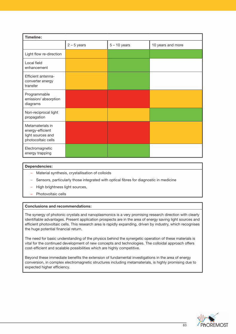
63
Timeline:
� – 5 years 5 – 10 years 10 years and more
Light flow re-direction
Local field enhancement
Efficient antenna-converter energy transfer
Programmable emission/ absorption diagrams
Non-reciprocal light propagation
Metamaterials in energy-efficient light sources and photocoltaic cells
Electromagnetic energy trapping
Dependencies:
Material synthesis, crystallisation of colloids
Sensors, particularly those integrated with optical fibres for diagnostic in medicine
High brightness light sources,
Photovoltaic cells
–
–
–
–
Conclusions and recommendations:
The synergy of photonic crystals and nanoplasmonics is a very promising research direction with clearly identifiable advantages. Present application prospects are in the area of energy saving light sources and efficient photovoltaic cells. This research area is rapidly expanding, driven by industry, which recognises the huge potential financial return.
The need for basic understanding of the physics behind the synergetic operation of these materials is vital for the continued development of new concepts and technologies. The colloidal approach offers cost-efficient and scalable possibilities which are highly competitive.
Beyond these immediate benefits the extension of fundamental investigations in the area of energy conversion, in complex electromagnetic structures including metamaterials, is highly promising due to expected higher efficiency.

64
2.4 NanofabricationNanoimprinting
Potential application domains:
Lighting and Displays
Information and Communication
Industrial Production/Manufacturing and Quality
–
–
–
Free-text keywords: Nano- and micro-optical components, miniaturized light sources and integrated opto-fluidic devices for sensors applications
Cross-references to other sections of document:
Subwavelength surface plasmon opticsMetamaterials in the visible rangeOpal templatingAutomotive lighting systemsNanoparticle-doped organics waveguide optical amplifiersMagneto-plasmonics for sensing applications
Date of Issue: April 08Institution and author’s name: Tyndall National Institute, Vincent Reboud & Nikolaos Kehagias
Context:
Polymer photonic devices aim to manipulate light at the micro- and nano-scale to create highly versatile systems. Although numerous systems have been demonstrated, recently alternative more cost-efficient processes such as nanoimprint lithography using low-cost polymer materials have been developed. Here we compare emerging nanopatterning methods and conventional ones for the realisation of polymer photonics. The potential application areas include communications, environmental lighting, sensing and opto-fluidic applications.
Motivation:
Nanoimprint lithography (NIL) as alternative fabrication technique In the last years, the main motivation of the field has been to show the capability of nanoimprint lithography [1] (NIL) to replace expensive and time-consuming techniques such as those based on electron-beam lithography and dry-etching methods. NIL and its related techniques have now demonstrated their capacity to fabricate organic photonic devices [�,3,4].
Cost effective patterning technique with sub-10 nm resolution Polymer waveguide-type wavelength filter based on a Bragg grating [5], microring resonator [6], lasers [7], plasmonic components, photonic crystals [8, 9] and more recently metamaterials have been recently realised showing the potential of NIL as a high-volume and cost-effective patterning technique with sub-10 nm resolution.
Direct fabrication of functional photonic integrated circuits Complex platforms of polymer photonic devices are still at the developmental stage. Progress is needed to produce full photonic integrated circuits with low-cost and high functionality. These photonic devices can be directly fabricated by NIL in the same materials during the same fabrication step [10]; or separately fabricated [11] and post-assembled. Another goal is the development of three-dimensional [1�] optical devices rather than planar structures to achieve a higher integration.
Mass production of large-area photonic circuits Investigation of the manufacturability of nanoimprinted polymer photonic devices for mass production of large-area photonic circuits. Roll-to-roll [13, 14], step-and-flash [15] and step-and-stamp [16, 17] techniques are most likely to meet the requirements for mass production.
–
–
–
–

65
Key performance figures:
Technique
Smallest/largest features in same print
Min pitch(nm)
Largest waferprinted (mm)
Overlay Accuracy (nm)*
T align,T print, T release, T cycle
Nr of times stamp used
Materials
NIL (thermal NIL)
5 nm a/ N/A
14 �00b 500
Minutes, 10s,Min, 10-15 min
> 50c various
SSILd(Step and Stamp Imprint Lithography)
8 nm min features.50 nm / 5 µm on same stamp
50 �00 < �50
Full cycle �.5 min with, �0 s without full auto collimation.
1000 Mr-I 8000, mr-I 7000
SFILe(Step and Flash Imprint Lithography)
�5 nmf / µm 50f300g,hstamp size: ~ �6x�6mm�
50 i(ca. �0i)
�0 wafers /hj
800g
VariousNILTM105, AMONIL, PAK 01
UV-NILk9nm/100µml
1�m �00n ca. �0p�0s/stepq3 wafers /hr
>1000s
MRT07xp,PAK01,AMONIL1,AMONIL�,NXR,Laromer
Soft UV-NIL�5nm / �0µmt
150u �00 1-50µmv4-5Min ca.1�wafer/hrw
>50xAMONIL1,NXR-Mod,Laromer
Activity in the field: High Dynamics: Expanding

66
References:
[1] CM Sotomayor Torres and J Ahopelto, Non Optical Lithography, Information Technology I, Vol.3, Chapter 7, Volume Editor: R. Waser, Wiley “Nanotechnology”, Series Editor: G. Schmid, H. Krug, R, Waser, V. Vogel, H. Fuchs, M. Grätzel, K. Lalyanasundaram and L. Chi. Berlin-Heidelberg, pp �09-�38 (�008).
[�] V. Reboud et al., Optics Express, 15, 1�, 7190 (�007).
[3] V. Reboud et al., Applied Physics Letters, 90, 011114, �007. Selected in Virtual Journal of Nanoscale Science & Technology, 15(3) (�007).
[4] V. Reboud et al., Applied Physics Letters, 91, 151101, �007. Selected in Virtual Journal of Nanoscale Science & Technology, 15(3) (�007).
[5] S.-W. Ahn et al., IEEE Photonics Technology Letters, vol. 17, 10 (�005).
[6] D.-H. Kim et al., IEEE Photonics Technology Letters, vol. 17, 11 (�005).
[7] D. Nilsson et al., Journal of Micromechanics and Microengineering, 15 �, �96, (�005)
[8] H. Schift et al., Nanotechnology16, S�61–S�65 (�005).
[9] M. Belotti et al., Microelectronic Engineering, 83 (4-9), 1773-1777 (�006)
[10] N. Chaix et, al,. Microelectronic Engineering, 84 (5-8) 880-884 (�007)
[11] W. Hu et al., Advanced Materials, 19, (16), �119 – �1�3 (�007)
[1�] N. Kehagias et al., Nanotechnology, 18, 175303, (�007)
[13] Kuwabara et al., Method of manufacturing a thin film pattern on a substrate, U.S. Patent 5 �59 0�6 (1993)
[14] H. Tan et al., J. Vac. Sci. Technol. B, 16(6), 39�6-39�8, (1998)
[15] M. Colburn et al., Proc. SPIE 3676-379, (1999)
[16] T. Haatainen et al., Emerging Lithographic Technologies IV, Proceedings of SPIE. Dobisz, Elizabeth. Vol. 3997. SPIE-The International Society for Optical Engineering, 874 – 880, (�000)
[17] T. Haatainen and J. Ahopelto, Physica Scripta. 67 (4), 357 - 360, (�003)

67
Key Performance Table:
(a) M.D. Austin et al, Appl. Phys. Lett. 2004, 84, 5299.
(b) C. Gourgon et al, J. Phys. D: Appl. Phys. 2005, 38, 70.
(c) This value is from manual tests. A cassette loading tool will have better values.
(d) Step and stamp imprint lithography is based on thermal NIL using the step and stamp imprinting tool, NPS300 by SUSS MicroTec.
(e) Step and flash imprint lithography.
(f) D. J. Resnick et al, “Step and Flash Imprint Lithography Templates for the 32 nm Node and Beyond”, NNT 06, San Francisco, US, Nov.15-17, 2006.
(g) M. Miller et al, “S-FIL Template Fabrication for Full Wafer Imprint Lithography”, NNT 06, San Francisco, US, Nov.15-17, 2006.
(h) T.-Wei Wu et al, “Nanoimprint Applications on Patterned Media”, NNT 06, San Francisco, US, Nov.15-17, 2006.
(i) S.V. Sreenivasan, et al, “Nano-Scale Mechanics of Drop-On-Demand UV Imprinting”, NNT 06, San Francisco, US, Nov.15-17, 2006.
(j) R. Hershey. et al, SPIE 2006, 6337-20.
(k) UV-NIL includes Single-Step
(l) B. Vratzov et. al., J. VacSci. Technol. B 2003, 21, 2760 and http://www.amo/de
(m) S.Y. Chou et al., Nanotechnology, 2005, 16, 10051
(n) 4 inch Single-Step, 8inch Step&Repeat on EVG770
(p) A. Fuchs, et. al., J.Vac. Sci. Technol, 2004, 22 and to be published.
(q) without fine alignment nor automation yet.
(r) http://www.molecularimprints.com
(s) M. Otto et. al., Microelectronic Eng. 2004, 73-74, 152.
(t) U. Plachetka, et. al., Microelectronic Eng. 2006, 83, 944.
(u) Pitch for Soft UV-NIL tested so far and to be published.
(v) Only coarse alignment available; depending on used stamp material
(w) 70-80% of the given time is to cure the resist.
(x) Based on laboratory tests to date.
–
–
–
–
–
–
–
–
–
–
–
–
–
–
–
–
–
–
–
–
–
–
–
Main scientific and technical challenges to be addressed:
After the successful demonstration of the first optical devices fabricated by NIL, one challenge is to extend this approach to mass production by the use of roll to roll, step and stamp, step and flash or/and, NIL on 8” wafers and demonstrate the reproducibility of the processes.
To subject nanoimprinted one- and two-dimensional planar polymer devices to environmental testing leading to high performarnce light extraction.
Development of cost-effective technique for the fabrication of optical components for the control of light in three directions.
The combination of optical and optoelectronic devices into opto-fluidic circuits.

68
Timeline:
� – 5 years 5 – 10 years 10 years and more
Mass production
High performance light extraction
Control of light in three directions
Opto-fluidic circuits
Dependencies:
Materials development: electrical pumping luminescent printable materials, printable conductive polymer.
Metrology and standards for the sub 50 nm scale.
Cost-efficient three-dimensional patterning methods. Mass-production of nanoimprinted polymer photonic devices
–
–
–
Conclusions and recommendations:
The research field of nanoimprint lithography, as exemplified here for polymer photonic devices is now characterized by a strong competition around the world. The work in the next years should focus on the development of next generation lithography as nanoimprint lithography for cost-efficient production of, for example, sub-wavelength optical components, super lens in the visible range, opto-fluidic circuits, three-dimensional optical components, to ensure European leadership in the field. Developments are needed to demonstrate the high throughput of the chosen fabrication processes as well in practical metrology techniques to enable the setting up of standards in nanomanufacturing.

69
2.5 Hybrid TechnologiesFunctional 1-D confined hybrid organic-inorganic nanotechnologies
Potential application domains:
Security, Metrology and Sensors
Lighting & Displays
–
–
Free-text keywords: Functionalisation, Self-assembly, Hybrid nanotechnologies, Plasmonics, Nanophotonics, Waveguiding, Inorganic nanostructures
Cross-references to other sections of document:
One-dimensional (1D) nanostructures: optical properties
Date of Issue: April 08Institution and author’s name: Tyndall National Institute (Colm O’Dwyer)
Context:
Optical integration, which promises high speeds and greater device versatility, remains a challenge in advancing nanophotonics. This section outlines recent advancements and summarises the properties and functions of individual inorganic nanostructures that are amenable to intercalation with organic molecules the functional groups of which can be employed in the uptake of semiconducting direct band gap quantum dots and emissive nanocrystals. Such structures may act as high aspect ratio, individually addressable emitters. The length, flexibility, and strength of these functionalisable structures enable their manipulation and attachment to surfaces, including the optical linking of nanoribbon/ wire/rod waveguides and other nanostructured elements to form networks, interconnects and device components. The bottom-up assembly of 1D confined nanostructures on processable CMOS-compatible substrates with nanowire light sources and detectors, could constitute a significant step toward building nanostructured electronic and photonic hybrid circuitry.
Motivation:
Low-dimensional metal-oxide nanostructures have attracted a considerable amount of research interest in recent years, but their use as photonic materials is still in its infancy. In addition to their ability to be functionalised with useful organic moieties, laminar turbostratic nanostructures are also excellent candidates for organic-inorganic hybrid composites which may possess multiple functionality. Both integrated optoelectronic devices and new nanocomposites can allow luminescent centre incorporation, tunable by varying the interlaminar distance and nanoparticle size, all controllable through synthetic means. Interlaminar spacing variation, diameter and length are currently controllable; the possibility of optically active nanoparticle incorporation makes them excellent candidates as photonically functional materials.Due to the random nature of the alignment dispersal of nanostructures on technologically suitable substrates, predetermined nanowire position remains a challenge. Some degree of control over the alignment can be achieved by utilizing electric-field assisted assembly. Although the methods used so far enable the study of the characteristics of single nanowire devices in order to demonstrate development potential, they cannot be easily scaled up for mass fabrication of dense, low-cost nanowire-based photodetector device arrays and emitters.

70
Key performance figures:
Nanoparticle incorporation in vanadium oxide nanotubes has only recently been demonstrated [1]. Nanoparticles uptake has been achieved in the interlaminar regions and not on the surface making them suitable candidates for waveguiding. CdS nanoparticles have also been synthesized within CdCl�-CTAB hybrid nanocomposites [�]. The optical gap of V�O5 has recently been confirmed to be 0.55 eV [3] but the absorption spectra is very rich with broad bands centred at 1.�5 and �.5 eV. For inorganic nanotubes, unprecedented control over length diameter and quality has been achieved. Nanotubes with lengths of several µm can have uniform diameters of ~100 nm. These findings are immediately applicable to other compound laminar systems.A new method for realizing high density spherical nanotube arrays [4], allows for an unprecedented density (40 sr-1) of highly uniform nanotubes. Similar metal-oxide nanostructures have been shown to be applicable as transparent electrodes and waveguiding by utilizing their wide band gap (3.6 eV for SnO�) [5,6].
Activity in the field: High Dynamics: Expanding
References:
[1] V. Lavayen, C. O’Dwyer, G. Gonzalez, G. Cardenas, and C. M. Sotomayor Torres, Mater. Res. Bull., 4�, 674 (�007).
[�] C. O’Dwyer, V. Lavayen, N. Mirabal, M. A. Santa Ana, E. Benavente, S. Ormazabal, G. Gonzalez, Z. Lopez, O. Schops, C. M. Sotomayor Torres, U. Woggon, Photon. Nanostruct.: Fundam. Applic., 5, 45 (�007).
[3] X. Liu C. Täschner, A. Leonhardt, M.H. Rümmeli, T. Pichler, T. Gemming, B. Büchner, M. Knupfer, Phys. Rev. B 7� 115407 (�005).
[4] C. O’Dwyer, V. Lavayen, E. Benavente, M. A. Santa Ana, G. Gonzalez, S. B. Newcomb, and C. M. Sotomayor Torres, Chem. Mater., 18, 3016 (�006).
[5] Materials Today, Volume 9, Issues 7-8, July-August �006, (The bright future of photonics) and articles therein.
[6] Materials Today, Volume 9, Issue 10, October �006, (Nanowires and nanotubes: Electronics and photonics in one dimension) and articles therein.
Main scientific and technical challenges to be addressed:
To control the size distribution of inorganic nanotubes to within 10%.
To anchor and position functionalised nanotubes on silicon platforms.
To design, fabricate and test a waveguide based on inorganic nanotubes functionalised with metal nanoparticles and/or semiconductor quantum dots.
Optical and electronic nano-scale addressing in a hybrid nanotube-silicon platform.
To determine experimentally the structure and chemistry of the nanotube at its anchoring point at the silicon substrate, to determine the charge distribution at the junction.
Functionalise inorganic nanotubes with luminescent centres including metal complexes, metallic nanoparticles, quantum dots and organic dyes with minimal bleaching during optical excitation.
Realise a fully functional, addressable electronic-photonic device using inorganic nanostructure waveguides and interconnects

71
Timeline:
� – 5 years 5 – 10 years 10 years and more
Controlled position of nanostructures
Quantum dot functionalised inorganic nanostructured waveguide
Optical and electronic nano-scale addressing
1D components with coupling
Subwavelength structures over large areas, integrated into device architectures
Dependencies:
Development of new materials
Development of processes that are compatible with current methods and device growth regimes
–
–
Conclusions and recommendations:
Single-crystalline 1D-confined low dimensional structures are intriguing tools with which to manipulate light, both for fundamental studies and photonics applications. As passive elements, they are efficient UV and visible waveguides and filters that can be assembled into optical networks and components. Being semiconductors or, in their doped state, transparent metals, oxide nanostructures are well suited to combine simultaneous electron and photon transport in active nanoscale components. Key challenges to the wider use of these materials include developing better parallel assembly schemes for nanowire integration on technologically useful substrates.

7�
Heterogeneous integration of III-Vs on silicon
Potential application domains:
Information and Communication
Design and Manufacturing of Components and Systems
–
–
Free-text keywords: Heterogeneous integration, silicon photonics, robust III-V wafers on silicon
Cross-references to other sections of document:
Automotive lighting systemsNanoparticle-doped organics waveguide optical amplifiers
Date of Issue: �8th March �008 Institution and author’s name: KTH, Sebastian Lourdudoss
Context:
One of the aims of silicon photonics is to integrate electronics and photonics for enhanced functionality. EU Technology Roadmap for Nanoelectronics [1], projects silicon or SOI (silicon on insulator) as the platform for integrating both electronic and photonic devices to form system-on-chip of the future. Efficient silicon based active optical devices being not viable in the near future, silicon photonics has to take a new turn in integrating Si/SiO� passive devices with other active optical devices, e.g., III-Vs. This approach has the great advantage of exploiting CMOS (Complementary Metal-Oxide-Semiconductor) compatible technologies. To achieve this goal, heterogeneous integration of III-Vs on silicon would be one of the routes.
Motivation:
We need to device a method which is generic so that it can even be applied to fabricate epitaxially relevant III-Vs on silicon or on silicon-on-insulator (SOI). Apart from the technical interest for achieving optical interconnects for high speed data transmission, the method can also be extended to fabricate GaN on silicon for cheap light sources for general lighting. Several methods including epitaxial lateral overgrowth (ELOG) by making use of different nanopatterned openings to take advantage of the nanoheteroepitaxial (NHE) effects are to be developed. Scientifically, combination of these two methods is a challenge. This would enable effective filtering of the defects from the interface propagating into the ELOG layer. These are the big challenges. To fabricate devices with long life-time there are additional challenges.
Key performance figures:
Defect density of e.g. InP grown on Si is ~ 1x105 cm-� [�]. However this material has been grown by liquid phase epitaxy is less flexible for production and the surface morphology remains largely to be improved. The defect density has to be reduced to at least 104 cm-�.There has been a reasonable success in InP devices wafer bonded to silicon [3,4] but the process flexibility and performance have to be improved.
Activity in the field: High Dynamics: Expanding

73
References:
[1] Techology Roadmap for Nanoelectronics, EU commision, �001.
[�] M. Sugai, T. Kochiya, Y. Oyama, J-I Nishizawa, Selective epitaxy of InP on Si(100) substrates prepared by liquid-phase epitaxy, Journal of Physics and Chemistry of Solids, vol. 69, pp. 411–414, �008.
[3] A. W. Fang, H. Park, O. Cohen, R. Jones, M. J. Paniccia, J. E. Bowers, “Electrically pumped hybrid AlGaInAs-silicon evanescent laser,” Opt. Express, vol. 14 (�0), pp. 9�03-9�10, �006.
[4] G. Roelkens, D. Van Thourhout, R. Baets, R. Notzel, and M. Smit, “Laser emission and photodetection in an InP/InGaAsP layer integrated on and coupled to a silicon-on-insulator waveguide circuit,” Opt.Express vol. 14, pp. 8154-8159, �006.
Main scientific and technical challenges to be addressed:
Reduce the defect density (EPD-Etch pit density) of III-V grown on silicon to less than 1x104 cm-�
Large area wafers of III-V on silicon (> 6 inch) can be grown; currently the technology for such a growth is available but not fully developed.
Simple integration of III-V active devices with silicon passive devices, e.g., detector and waveguide
CMOS compatible process for integrating active III-V photonic devices with silicon electronic circuits - very hard due to the mismatch in processing temperature windows for CMOS and III-V technologies; besides the lack of flexibility of the CMOS fabrication laboratories to adapt to new designs is also a handicap
Timeline:
� – 5 years 5 – 10 years 10 years and more
Reduction of EPD
Large area (>6”) wafers
Simple integration of active and passive devices
CMOS compatible process of monolithic integration of III-V on silicon
Dependencies:
Optimisation of nanoimprint technology for achieving ELOG of III-V on silicon
Development of III-V epitaxial reactors that would accommodate wafers larger than 6 inch
Adaptation willingness of CMOS fabrication centres to accommodate III-V technologies
–
–
–
Conclusions and recommendations:
Heterogeneous integration through wafer bonding is one approach but monolithic integration should be given considerable thrust as it enables large size wafers of III-V on siliconAdaptation of CMOS fabs for handling III-V processes would largely facilitate monolithic integration and silicon photonics

74
Integration of colloidal photonic crystals
Potential application domains:
Design and Manufacturing of Components and Systems
Security, Metrology and Sensors
Life Sciences and Health
–
–
–
Free-text keywords: Photonics, sensor cavities, all optical chips
Cross-references to other sections of document:
Non-linear nano-optics IPhysics and applications of random lasersOpal templatingModelling and optimization in opal-based photonic crystals
Date of Issue: April �008Institution and author’s name: VTT, Sanna Arpiainen; Tyndall National Institute, Gudrun Kocher
Context:
The research in colloidal PhCs is entering the utilization phase where their integration with other photonic components is essential. 3D PhCs can be potentially utilized as porous optical detection cavities in Lab-on–Chip and other sensor applications and in various signal processing tasks in integrated optics, eventually enabling the realization of all-optical microchips. The fabrication of integrated colloidal 3D photonic crystal components necessitates the development of spatially selective growth methods for 3D templates, controlled incorporation of defects and inversion process compatible with the photonic chip.
Motivation:
Due to the translational symmetry perpendicular to the direction of propagation (as compared to cavities in �D PCs), 3D high-Q optical cavities can be constructed without birefringence for filtering applications. Due to the large void space and sensitivity to minor changes inside this space or in the incorporated defects, such optical cavities are ideal in sensor applications. However, the use requires that single crystalline 3D crystals be integrated in the photonic chip in a controlled manner and, furthermore, that a well defined pattern of point defects can be defined inside the PC. The 3D PCs can be fabricated either by lithographic means or by self-assembly. Most of the lithographic methods directly facilitate also the defect inscription inside the PC, but are somewhat limited either by the speed of processing or by the resolution, though in some cases this is expected to change in the future. Self assembly methods can be designed to be low cost, fast and scalable, but the definition of deterministic defects has still to be accomplished by lithographic means. The spatially selective self-assembly of the opal template can be accomplished by capillary directed deposition techniques, where pre-defined capillary channels direct the colloidal micro-/nano-particles into the desired positions. However, major improvements, like combining the method with on-chip electrophoresis (on wafer scale during production) and lithographically patterned templates on the substrate are still required for the yield of the method for producing single crystalline opals with desired orientation.Defect fabrication can be based either on sequential growth, where the defect layer is deposited on top of the lower half of the opal and patterned before the deposition the upper half, or it can be based on subsequent defect inscription inside the opal. Both of these methods are rather challenging, but the former can potentially be scaled up for large scale production. For the performance of the photonic component, the quality of the �D defect lattice inside the 3D PC is of utmost importance. Light emitters have also been successfully embedded in inverted opal structures which is an important step towards optical integration.

75
Key performance figures:
Spatially selective deposition of colloidal crystals scaleable to wafer size [3,13]
Theoretical modelling of integrated structures and planar defect structures for hybrid 2D/3D architectures [4,5]
Realisation of planar and deterministic defects by micromanipulation, electron beam lithography and two-photon manipulation [6-11]
Inscription of a waveguide in a 3D opal [11’]
Light emitter embedded in inverted opal structures [12]
–
–
–
–
–
Activity in the field: High Dynamics: Stationary
References:
[1] N. Tétreault et al Adv. Mat. 16, 1471 (�004)
[�] B. H. Juárez et al Adv. Mat. 17, �761 (�005)
[3] J. Ye et al Langmuir �� (17), 7378, (�006)
[4] A. Chutinan et al Physical Review E, 71(�) (�005)
[5] K. Vynck et al Optics Express 14 (15) 6668 (�006)
[6] P. Massé et al Chem. Phys. Lett. 4��, �51 (�006)
[7] H. T. Miyazaki et al J. of Appl. Phys. 87, 715� (�000)
[8] G. Kocher et al Solid State Electronics 51, 333 (�007)
[9] W. Cai et al Appl. Phys. Lett. 88, 11111� (�006)
[10] Y. Jun etr al Adv. Mat. 17, 1908 (�005)
[11] F. Fleischhaker et al JASC 1�7, 9318 (�005)
[1�] SA Rinne Nature Photonics �,5� (�007)
[13] D. Garcia et al Adv. Mat. 18, �768 (�006)
[14] Patent application ”CAPILLARY TRANSPORT OF NANOPARTICLES OR MICROPARTICLES TO FORM AN ORDERED STRUCTURE” FI �0075153 by Fredrik Jonsson, Jouni Ahopelto, Sanna Arpiainen & Clivia Sotomayor Torres, (�007).
Main scientific and technical challenges to be addressed:
Reproducible inverted opals showing a full photonic bandgap on spatially selective deposited opal templates: inversion process complicated due to multiple thermal interfaces in pre-patterned silicon/silica/opal template structure;
–
Emitters embedded inside the inverted opal: experimentally prove the theoretical prediction of modification in the spontaneous emission rate; processes for high precision fabrication methods.
–
Design of devices with special emphasis on their functionality, optical confinement and coupling: 3D simulations currently very time consuming.
–
Design of optical equivalents to diodes and transistors compatible with Si technology: new and innovative design needed to find an optical equivalent to the electronic: http://arxiv.org/abs/0803.�595v�
–

76
Timeline:
� – 5 years 5 – 10 years 10 years and more
Controlled embedding of emitters in inverted opal
Reproducible inverted opals on patterned templates
All optical switches and amplifiers compatible to Si technology
Dependencies:
New and innovative design needed for all optical switches and amplifiers compatible to Si technology.
Mastering multiple thermal interfaces for inversion of integrated 3D PhC structures
–
–
Conclusions and recommendations:
The fabrication of colloidal photonic crystals is cheap, fast and scaleable to wafer size, but methods still need to be improved by, e.g., combining the capillary directed deposition, like capillary directed self-assembly (CDSA) with electrophoresis and lithographically patterned templates on the substrate to improve the yield of single crystalline opals with desired orientation.In comparison with fibre optic components or stand alone �D PhCs, integrated 3D self assembled PhCs with embedded defects, cavities and emitters provide potential for much wider functionality in operation.

77
Magnetophotonic crystals
Potential application domains:
Design and Manufacturing of Components and Systems
Information and Communication
–
–
Free-text keywords: Photonic crystals, Magnetophotonic crystals, Infiltrated opals
Cross-references to other sections of document:
Functionalization for photonic biosensingOpalsMagneto-plasmonics for sensing applications
Date of Issue: �0 March �008 Institution and author’s name: VPU, Rimas Vaisnoras
Context:
This entry focuses on fabrication and testing of photonic crystals with magnetic materials for novel magnetophotonic device prototyping. It responds to the growing interest in photonic crystals for device applications based on their unique photonic band gap properties. There is particular need to explore the use of photonic crystals as magnetic systems, since most of present work in this area addresses primarily the use of non-magnetic materials. Organic/inorganic compounds containing magnetic ions make these materials a unique choice for the fabrication of magnetophotonic crystals (MPCs) controlled with external magnetic field. Photonic crystal structures provide a novel alternative to address this problem since it is possible to build optoelectronic devices, a generation ahead of the types being explored at present. By establishing a practical implementation of MPCs, various components in optoelectronic systems could be developed including optical filters, switches, efficient Kerr reflectors for magneto-optical recording and biosensors.
Motivation:
Combining organic and inorganic compounds containing magnetic ions, photonic crystals with novel optical and magnetooptical properties can be fabricated. There is a special interest for hybrid magnetophotonic crystals with properties that can be controlled by an external stimulus (laser light, temperature, magnetic field, etc.).Due to specific features of electromagnetic wave propagation in photonic crystals, enhanced light-matter interaction in nanoscale systems is expected. Enhancement of electromagnetic waves at the sample surface, metal nanoparticles and defects in photonic crystals would have crucial impact on enhanced spectroscopy, efficient generation of higher harmonics, enhanced electro- and magneto-optical effects. By combining spectroscopic features of constituent materials with particular features of light propagation in magnetophotonic crystals, the efficiency of optoelectronic elements is expected to be strongly improved.An image-based method for label-free detection of biomolecules on the surface of a photonic crystal is used for development of new of type biosensors with high sensitivity and other elements in biotechnology. An improved functionality of biosensors for a wide variety of biochemical and cell-based assays is expected in MPCs.
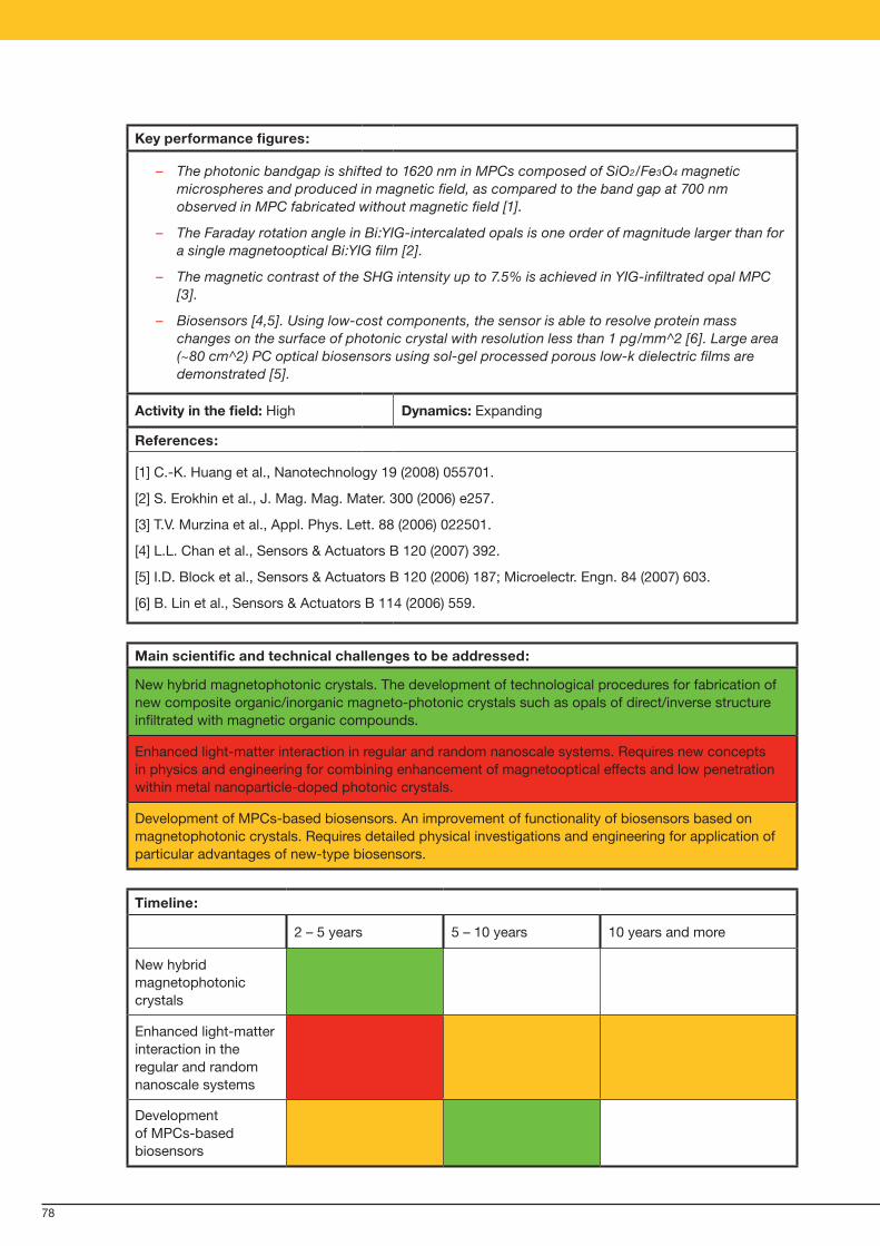
78
Key performance figures:
The photonic bandgap is shifted to 1620 nm in MPCs composed of SiO2/Fe3O4 magnetic microspheres and produced in magnetic field, as compared to the band gap at 700 nm observed in MPC fabricated without magnetic field [1].
The Faraday rotation angle in Bi:YIG-intercalated opals is one order of magnitude larger than for a single magnetooptical Bi:YIG film [2].
The magnetic contrast of the SHG intensity up to 7.5% is achieved in YIG-infiltrated opal MPC [3].
Biosensors [4,5]. Using low-cost components, the sensor is able to resolve protein mass changes on the surface of photonic crystal with resolution less than 1 pg/mm^2 [6]. Large area (~80 cm^2) PC optical biosensors using sol-gel processed porous low-k dielectric films are demonstrated [5].
–
–
–
–
Activity in the field: High Dynamics: Expanding
References:
[1] C.-K. Huang et al., Nanotechnology 19 (�008) 055701.
[�] S. Erokhin et al., J. Mag. Mag. Mater. 300 (�006) e�57.
[3] T.V. Murzina et al., Appl. Phys. Lett. 88 (�006) 0��501.
[4] L.L. Chan et al., Sensors & Actuators B 1�0 (�007) 39�.
[5] I.D. Block et al., Sensors & Actuators B 1�0 (�006) 187; Microelectr. Engn. 84 (�007) 603.
[6] B. Lin et al., Sensors & Actuators B 114 (�006) 559.
Main scientific and technical challenges to be addressed:
New hybrid magnetophotonic crystals. The development of technological procedures for fabrication of new composite organic/inorganic magneto-photonic crystals such as opals of direct/inverse structure infiltrated with magnetic organic compounds.
Enhanced light-matter interaction in regular and random nanoscale systems. Requires new concepts in physics and engineering for combining enhancement of magnetooptical effects and low penetration within metal nanoparticle-doped photonic crystals.
Development of MPCs-based biosensors. An improvement of functionality of biosensors based on magnetophotonic crystals. Requires detailed physical investigations and engineering for application of particular advantages of new-type biosensors.
Timeline:
� – 5 years 5 – 10 years 10 years and more
New hybrid magnetophotonic crystals
Enhanced light-matter interaction in the regular and random nanoscale systems
Development of MPCs-based biosensors

79
Dependencies:
Material specification for optimised Faraday rotation
Device concepts
Integration strategies
–
–
–
Conclusions and recommendations:
Nanophotonics is a rapidly expanding field with many potential applications. Magnetophotonics offers key advantages with respect to non-magnetic photonic crystals presenting new functionalities and new aspects for application. The need for basic understanding of the magneto-optics at the nanoscale and for development of new techniques is the key for revealing of the optimal specific applications and for realisation of the advantages of magnetophotonic crystals.

80

81
03Emerging Devices

8�
3. Emerging Devices2.1 Infiltration TechniquesHybrid organic– nanoparticle solar cells
Potential application domains:
Energy conversion–
Free-text keywords: Photovoltaics, quantum nano dots, polymer solar cells
Cross-references to other sections of document:
Assemblies of colloidal quantum dots One-dimensional (1D) nanostructures: optical properties Colloidal crystals for light manipulation
Date of Issue: 10/06/07 Partner: Jordi Martorell, ICFO
Context:
Photovoltaics is becoming increasingly recognized as part of the solution to the growing energy challenge and an essential component of future energy production. The big drawback is the rather high production cost. In this context is where the hybrid technology that combines polymer and nanoparticles comes into play. In addition, such photovoltaic technology is compatible with plastic or any kind of flexible material.
Motivation:
Energy from the sun is the alternative capable of providing a response to an ever increasing energy demand. At a world level, the energy consumption is 13 TW, and it is forecasted that such consumption will rise up to 30 TW by the year �050. Such an extraordinarily large figure is well below the 1�0,000 TW from the sun that reach the surface of the earth. Currently, commercial silicon cells convert an average of 15% of the solar light into electricity, at an approximate cost of 300Euro/m� of solar panel.It is clear to many that an alternative form for converting solar light to electricity is needed. There are, essentially, two technologies that are being considered to either replace or complement the crystalline silicon based photovoltaic cells. One is based on dye sensitized solar cell and the other is based on organic materials.Organic solar cells do offer many advantages to become a widespread technology for electricity production. Among these it is worth highlighting that: Organic molecules are cheap to fabricate and organic materials are compatible with plastic or any other kind of flexible materials. There still remains the challenge to boost up the efficiency of organic solar cells.Quantum dots are small semiconductors with a tunable band gap that in contrast to traditional semiconductors can be molded in a variety of different forms. They can be combined with organic polymers and be processed to create junctions on inexpensive substrates such as plastics.

83
Key performance figures:
The top efficiency of organic solar cells (<5%) is yet well below the efficiency from alternative technologies such as dye sensitized solar cells or CIGS(Copper Indium Gallium Selenide) solar cells.[1]
In 2002 the group of A. P. Alivisatos proposed a new hybrid nanorod-polymer solar cell with a monochromatic power conversion of 6.9%.[2]
Konarka Technolgies Inc. and Evident Technnologies have formed a joint research program to develop ultra-high performance plastic solar cells and make such devices a comercial reality. Konarka’s polymers are to be combined with Evident’s quantum dot nanotechnology to increase the sensitivity of the cells to a wider range of the light spectrum. Specifications of the products are yet to be announced. The company stated goal was a 10% efficiency.[3]
Organic solar cell devices could be fabricated with low-cost, high throughput printing techniques that consume less energy and require less capital investment than crystalline silicon based devices and other thin-film technologies. The factor of cost production was estimated that it could be reduced by a factor of 10 or 20. This will soften the need for high efficiencies to make such type of solar cells commercial.
–
–
–
–
Activity in the field: High Dynamics: Expanding
References:
[1] H. Hoppe and N. S. Sariciftci, J. of Mat. Res. 19, 19�4 (�004).Solar Energy Materials & Solar Cells 91 (�007) 4�0–4�3 (�007)
[�] Huynh WU, Dittmer JJ, Alivisatos AP, Science �95, �4�5-�4�7 (�00�)H. Hoppe and N. S. Sariciftci, J. of Mat. Res. 19, 19�4 (�004).
[3] http://www.konarka.com/
Main scientific and technical challenges to be addressed:
Enhance the efficiency of the conversion from solar to electrical energy. This requires the development of new composite materials such as conjugated polymers mixed with quantum dots
Another major challenge that the technology of plastic solar cells and organic solar cells face is the poor stability and longevity. Apart from chemical decomposition of the organic molecules, organic solar devices can degrade from distortion, loss of adhesion of the layers, or the layers diffusing into each other. Engineering more stable molecules is needed to substantially improve the lifetime of the device. The hybrid organic-inorganic solar cell has a better perspective in that sense, and progress is being made on this front.
Develop the appropriate procedures to fabricate plastic solar cells at a low cost without a significant reduction of the efficiency with respect to the laboratory prototypes. In general, with the currently available technology, efficiency diminishes by more than a factor of � when lab prototypes are brought into a production line.
Timeline:
� – 5 years 5 – 10 years 10 years and more
Enhance the efficiency
Improve the lifetime of the device
New procedures to fabricate plastic solar cells

84
Dependencies:
Development of new materials
Development of appropriate encapsulation techniques and approaches
–
–
Conclusions and recommendations:
The hybrid polymer-nanoparticle solar cell is a technology that offers two key advantages with respect to the commercially available silicon cells. On the one hand, a low production cost and on the other hand, the possibility to fabricate devices that may adapt to plastic or any other kind of flexible material.
We believe it is worth investing resources in that technology given the high yield returns that are expected in an economical sense as well as, in general, to the global energy scenario.

85
Automotive lighting systems
Potential application domains:
Lighting and Displays–
Free-text keywords: interior and exterior lighting; stand-alone lighting systems; flexible smart films; enhanced lifetime
Cross-references to other sections of document:
Assemblies of colloidal quantum dots Colloidal crystals for light manipulation Heterogeneous integration of III-Vs on silicon Nanoimprinting
Date of Issue: �5/03/�008 Institution and author’s name: Vito Lambertini, CRF
Context:
The integration of stand-alone, flexlible, thin and high lifetime lighting systems will have a great impact on the automotive market in term of improved vision and driving confort, reduced fuel consumption and related polluttants emissions, increased safety...
Motivation:
The current automotive lighting systems are based on standard bulb lamps which result in heavy and power consuming devices. The chip LEDs introduction started few years ago with great advantages in terms of reduced volume, power consumption and higher lifetime. Nevertheless the today bottlenecks are related to the costs of the overall lighting systems which include LEDs and integration costs. While the cost of LEDs is reducing fast, still remain a great lack of integrated technologies in order to produce stand-alone, very thin and low cost devices.
The actual challenge in the automotive lighting market (front light, tail light, courtesy lighting systems and dashboard displays) is the integration of new photonic technologies allowing high brightness and high lifetime with manufacturing routes allowing low cost fabrication.
The compactness of the lighting systems will result in reduced plastic consumption and therefore lower environmental impact. Lighter and stand-alone devices will have impact on the fuel consumption with a potential reduction in the range 10-15% with related reduced CO� and exhaust gases production. Furthermore, energy saving inherent to the efficiency of LED sources, will also contribute to the preservation of natural resources.
Improvement in vehicle lighting allows to improve vision and driving comfort, thus reducing the occurrence of accidents and increasing safety. Fall-outs to signalling and information displays will also lead to more efficient information delivery and better usability of information systems.
–
–
–
–
Key performance figures:
Materials used in organic electronics [1]
Printing or printing like processes enabling new high volume/ low cost deposition techniques [1]
Review of techniques for manufacturing organic electronic devices analyzed with respect to cost and market fitness [2]
–
–
–
Activity in the field: High Dynamics: Expanding

86
References:
[1] Organic Electronic Association (OE-A) review (1st and �nd edition, �006 and �007)
[�] Manufacturing and commercialization issues in organic electronics, James R. Sheatsa, J. Mater. Res., Vol. 19, No. 7, �004
Main scientific and technical challenges to be addressed:
Setting up of low-cost manufacturing methods for intelligent plastic films including an electronic core connected to input/output devices (sensors, Radio Frequency Identification RFID, display) and energy source/storage.
Production of wireless and medium/high brightness systems to be integrated in several automotive interiors and exteriors devices.
Low cost integration and assembling technologies to produce fully autonomous lighting systems.
Timeline:
� – 5 years 5 – 10 years 10 years and more
Low-cost manufacturing methods
Wireless and medium/high brightness systems
Integration and assembling
Dependencies:
Integration of new photonics technologies with low cost manufacturing process.
Assembling of intelligent plastic films with multifunctional properties.
–
–
Conclusions and recommendations:
The autonomous systems in automotive represent a great innovation with impact at several level: comfort, safety and energy consumption. The development of efficient and stable photonic devices is the base for the production of such devices. Moreover the optimization of technologies in terms of deposition, integration and assembling must be emphasized in order to get devices at low cost.

87
Nanoparticle-doped organics waveguide optical amplifiers
Potential application domains:
Information and Communication
Design and Manufacturing of Components and Systems
–
–
Free-text keywords: Polymethylmethacrylate PMMA waveguides, waveguide optical amplifiers, QDs hybrid materials, hybrid nanotechnologies, Er-doped PMMA
Cross-references to other sections of document:
Assemblies of colloidal quantum dots One-dimensional (1D) nanostructures: optical properties Nanoimprinting Heterogeneous integration of III-Vs on silicon
Date of Issue: 03/�5/�008Institution and author’s name: CoreCom, Silvia M. Pietralunga
Context:
Prototypes of waveguide optical amplifiers at telecomm wavelengths, based on hybrid nanotechnology have been realized and tested. Two distinct PMMA-based technologies are addressed:
amplification in the third telecomm window around λ = 1.5µm is provided by PMMA matrix with dispersed Er-doped nanoparticles, by optical pumping at 980nm. Single mode amplifying rib waveguides have been realized by optical lithography and reactive ion etching.
amplification in the second telecomm window around λ = 1.3µm is achieved by doping PMMA with dispersed lead chalcogenide PbSe nanodots. In this case, high gain coefficient has been proved for the material in slab geometry.
–
–

88
Motivation:
Integrated optics waveguide amplifiers are expected to provide optical gain over short propagation distance, to target applications in optical chips and subsystems for optical interconnections.
Advantages of PMMA include: the possibility to obtain high core/cladding refractive index contrasts by cost-effective fabrication processes like molding, casting, stamping and embossing; the possibility of being deposited and processed on any kind of substrate, then allowing for integration with other optical functionalities on the same chip; high transparency in the near infrared; simple and fast fabrication of 3-D circuits with vertical couplers; thermal stability of transmission properties of singlemode waveguides ( assessed by accelerated aging tests performed at �00°C for �000 hours).
For amplification in the third telecomm window around λ = 1.5µm (Erbium-Doped Waveguide Amplifiers) EDWAs have already been implemented in inorganic matrices, both oxides and semiconductors, but most of related fabrication processes involve either numerous or critical and expensive steps that may result in long elaboration time and high costs. Also electrically-pumped quantum-dots amplifiers made of III-V InGaAs/GaAs structures grown by molecular beam epitaxy have been proposed; here the drawbacks are the issues and costs involved by the lattice-matched epitaxial growth process, and the large QD diameters compared to the Bohr exciton diameter, involving closely-spaced atom-like states, affecting temperature stability of lasing wavelength and significant size-effect tuning.
The development of optical telecomm and datacomm systems employing Wavelength Division Multiplexing (WDM), where the wavelength spacing between channels is > �0nm and the transmission window around λ = 1.3µm is also used, pushes the demand of low-cost solutions for optical amplification over an ultrabroad wavelength range to be implemented at the chip level. Optical amplifiers containing nano-sized semiconductor quantum dots can be an answer to this, since they operate over a few hundreds of nm, they show low noise figure and high saturation output power and fast gain response, what allows for the suppression of signal distorsion and noise reduction.
Monodisperse colloidal lead chalcogenide quantum dots (1÷10nm) feature energy levels spacing by hundreds of meV, and result in size-tunable optical amplification bands potentially ranging between 850nm and 1800nm. They operate under optical pumping like erbium-doped amplifiers, and amplified spontaneous emission has been recently reported under 980nm CW pumping. They are compatible with a wide range of substrates from crystalline to amorphous, rigid to flexible, and they can be easily used as active dopants in amorphous polymer matrices.
–
–
–
–
–
Key performance figures:
Optical gain coefficient for the material: o for Er-doped PMMA pumped at 980nm: 0.9cm-1 @ λ = 1540nm [1]o for PbSe/PbS QD-doped PMMA pumped at 980nm: 6.6÷6.8cm-1 @ λ = 1255nm. Gain threshold 1.4W/
cm2 [2]
Waveguide propagation loss: o for Er-doped PMMA rib waveguide: 1.3dB.cm-1 at 1540nm [3].
Net optical gain coefficient in waveguide: o for Er-doped PMMA: 1.34dB @ λ = 1.540nm is demonstrated for a 1.6cm - long single-mode waveguide
amplifier [3]
–
–
–
Activity in the field: High Dynamics: Expanding
References:
[1]A. Q. LeQuang et al., Proc. SPIE, 61�3, 61�30� (�006)
[�]E. Lifshitz et al. J. Phys. Chem B, 110, 50, �5356 (�006)
[3] A. Q. LeQuang et al., APL, 89, 1411�4 (�006)

89
Main scientific and technical challenges to be addressed:
Increased gain of PMMA-based EDWA at λ = 1.5µm Larger gain at λ = 1.5µm can be expected by increasing erbium quenching concentrations using other ligands or by introducing sensitizers such as ytterbium or cerium.
Realization of PMMA-based WDM coupler Integrated optics WDM couplers for coupling/decoupling the pump wavelength at 980nm with the signal at λ = 1.5/1.3µm are mandatory to the integration of the waveguide amplifiers within optical circuits and in view of plug-and-play devices.
Chalcogenide doped single-mode waveguides Promising optical gain coefficients have been demonstrated in PbSe chalcogenide QD dispersed in PMMA matrix, but no single-mode waveguide has been implemented up to now to experimentally verify the integrated optics processability of this specific material and final performances of the device
Plug and play devices PMMA waveguide amplifiers on chosen substrates have to be designed for production, implemented and packaged. Self-standing devices can be realized, with input/output optical connectors or fiber pigtails. As an alternative, technological solutions for hybrid integration of PMMA technology onto other integrated-optics processes ( i.e. silicon optics or silica-on-silicon PLC Photonic Lightwave Circuit) must be developed.
Timeline:
� – 5 years 5 – 10 years 10 years and more
Increased gain of PMMA-based EDWA at 1.5µm
Realization of PMMA-based WDM coupler
Chalcogenide doped single-mode waveguides
Plug-and-Play devices
Dependencies:
Optimization of PMMA-based material quantum electronics properties for maximization of gain coefficient
–
Conclusions and recommendations:
The market scenario for optical interconnections (short and medium haul) presently demands low-cost technological solutions for amplifying integrated-optics devices at telecomm wavelengths. PMMA-based amplifiers can actually be a solution to this. Synergic research efforts of involved research centers are necessary and strongly recommended, for a timely assessment of the level of performances that can be offered by the present technology. The production of plug-and-play performing prototypes within 5÷6 years from now will enable to enter the market.

90
Magneto-plasmonics for sensing applications
Potential application domains:
Information and Communication
Life Sciences and Health
Lighting and Displays
Security, Metrology and Sensors
–
–
–
–
Free-text keywords: Active plasmonic devices. Enhanced sensitivity surface plasmon resonance sensors
Cross-references to other sections of document:
Subwavelength surface plasmon opticsNanoimprintingMagnetophotonic crystals
Date of Issue: 08/06/07 Institution and author’s name: IMM-CSIC, Alfonso Cebollada
Context:
Magneto-Plasmonics is a discipline that aims at studying the optical and magneto-optical activity of structures where noble metals exhibiting strong surface plasmon resonances are combined with ferromagnetic materials. The optical properties characteristic of plasmonic structures can then be actively controlled by an external magnetic field. This opens a wide range of applications such as active subwavelength optical devices, higher sensitivity optical sensors, etc…
Motivation:
Existing nanoplasmonic structures and devices act as passive elements in their modification of light. The possibility of generating active nanoplasmonic devices would open new lines of research and make available higher performance devices. The incorporation of magnetic elements is feasible and the subsequent plasmonic properties could be controlled and tuned by an external magnetic field.
Key performance figures:
Current sensitivity of SPR: 10-5 in refractive index changes
Expected sensitivity of MSPR: 10-6 in refractive index changes
–
–
Activity in the field: High Dynamics: Expanding
References:
[1]Highly sensitive detection of biomolecules with the magneto-optic surface-plasmon-resonance sensor”, B. Sepúlveda et al., Optics Letters, vol 31 No 8 (�006) 1085
Main scientific and technical challenges to be addressed:
New field: explore all the physics involved and subsequent applications.
Extend the applicability of these devices to a wide range of radiation wavelengths beyond the visible range, to broaden the applicability options ( microwave).
Range of control of the plasmonic activity with an external magnetic field

91
Timeline:
� – 5 years 5 – 10 years 10 years and more
Physics and applications
Extend wavelengths
Plasmonic activity control
Dependencies:
FIB (Focused ion Beam)to fabricate necessary nanodevices.
New theoretical tools.
Control on growth quality.
–
–
–
Conclusions and recommendations:
This is very promising area of research, with a niche for applications in the field of telecommunications and sensors. It is, however, in a proof of concept stage and therefore needs to demonstrate its real applicability. From the basic science point of view it will help to understand both plasmonic and magneto-optical phenomena in novel hybrid structures.

9�
Technical Acronyms
Acronym Full Name1D One dimension�D Two dimensions3D Three dimensionsALD Atomic Layer DepositionASE Amplified Spontaneous EmissionCBD Chemical Bath DepositionCIGS Copper Indium Gallium SelenideCMOS Complementary Metal Oxide SemiconductorCVD Chemical Vapour DepositionCW Continuous WaveDBR Distributed Bragg Reflector EDWA Erbium-Doped Waveguide AmplifierELOG Epitaxial Lateral OvergrowthFIB Focused Ion BeamFRET Foerster Resonant Energy TransfersIR Infra RedLED Light Emitting DiodeMPCs Magnetophotonic CrystalsOE-A Organic Electronic AssociationOLED Organic Light Emitting DiodeNHE NanoheteroepitaxialNIL Nanoimprint lithographyNIR Near InfraredPBG Photonic BandgapPhCs Photonic Crystal Structures PLC Photonic Lightwave CircuitPMMA PolymethylmethacrylatePND Plasmon NanodevicesQ Quality factorQD Quantum DotRFID Radio Frequency IdentificationRCLE Resonant cavity light-emitting diodeSCNC Semiconductor NanocrystalSERS Surface Enhanced Raman ScatteringSFIL Step and Flash Imprint Lithography SHG Second Harmonic Generation SOI Silicon on InsulatorSP Surface plasmons SSIL Step and Stamp Imprint LithographyTHG Third Harmonic GenerationUV UltravioletVCSEL Vertical cavity surface emitting laserWDM Wavelength Division Multiplexing

93
Contributors
Name Institution Acronym
Arpiainen, Dr. Sanna Technical Research Centre of Finland VTT
Cebollada, Dr. AlfonsoInstituto de Microelectrónica de Madrid (Consejo Superior de Investigaciones Científicas)
IMM (CSIC)
Dholakia, Prof. Kishan University of St. Andrews St. Andrews
Dunkin, Dr. AlexanderIoffe Physico-Technical Institute of the Russian Academy of Sciences
Ioffe-SP
Gaponik, Dr. Nikolai Technische Universitat Dresden TU-Dresden
Gergely, Prof. Csilla Universite Montpellier � UM�
Hickey, Dr. Stephen Technische Universitat Dresden TU-Dresden
Kehagias, Dr. Nikolaos Tyndall National Institute Tyndall
Kocher, Dr. Gudrun Tyndall National Institute Tyndall
Kurdyukov, Dr. DmitryIoffe Physico-Technical Institute of the Russian Academy of Sciences
Ioffe-SP
Lambertini, Dr. Vito Centro Ricerche Fiat Societa’ Consortile Per Azioni CRF
Lopez, Prof. CefeInstituto de Ciencia de Materiales de Madrid (Consejo Superior de Investigaciones Científicas)
ICMM (CSIC)
Lourdudoss, Prof. Sebastian Kungliga Tekniska Hogskolan KTH
Malvezzi, Prof. Marco Universita degli Studi di Pavia Upavia
Martorell, Prof. Jordi ICFO-Institut de Ciencies Fotoniques ICFO
O’Dwyer, Dr. Colm Tyndall National Institute Tyndall
Pietralunga, Dr. Silvia M.Consorzio Ricerche Elaborazione Commutazione Ottica Milano
CoreCom
Quidant, Dr. Romain ICFO-Institut de Ciencies Fotoniques ICFO
Reboud, Dr. Vincent Tyndall National Institute Tyndall
Romanov, Dr. Sergei Tyndall National Institute Tyndall
Serpengüzel, Prof. Ali Koç University Koç
Sibilia, Prof. Concita Universita Delgi Studi Roma “La Sapienza” UR-DE
Vaisnora, Dr. Rimas Vilnius Pedagogical University VPU
Vynck, Dr. Kevin Universite Montpellier � UM�
Wiersma, Dr. Diederik European Laboratory for Non-Linear Spectroscopy LENS
Woggon, Prof Ulrike University of Dortmund Uni-Do

94
Subject IndexA
acoustic fields .............................................................................................................................................................. 44
all-optical ................................................................................................................................................... 34, 5�, 59, 71
amplifiers....................................................................................................................................................73, 8�, 83, 84
antennas ................................................................................................................................................................59, 60
ASE.......................................................................................................................................................................................50
B
bio-imaging .................................................................................................................................................................. 16
biological agents.................................................................................................................................................... �4, �5
biomolecules .................................................................................................................................. �1, 38, 39, 50, 74, 85
bio-sensing .................................................................................................................................................................. 38
biosensor .........................................................................................................................................................38, 39, 40
Bose-Einstein condensation ..................................................................................................................................... 8, 9
bottom up................................................................................................................................................... 13, 48, 55, 58
Bragg reflectors ............................................................................................................................................................. 8
C
CBD .............................................................................................................................................................................. 34
coherence
quantum .................................................................................................................................................................... 9
colloidal ......................... 19, �6, �8, 31, 34, 41, 4�, 44, 45, 46, 48, 49, 50, 51, 5�, 55, 56, 58, 61, 71, 7�, 73, 77, 80, 8�
colloidal systems ......................................................................................................................................................... �6
composite .................................................................................................................................................. 34, 36, 75, 78
confinement of light ....................................................................................................................................................... 8
correlated photons ................................................................................................................................................ 19, �0
CVD ............................................................................................................................................................ 1�, 34, 35, 87
D
defect inscription ......................................................................................................................................................... 71
demultiplexer ............................................................................................................................................................... 5�
diffraction limit ........................................................................................................................................................11, �9
diffusive materials ........................................................................................................................................................ 33
displays .................................................................................................................................................. 9, �9, 31, 46, 80
divergence
beam ......................................................................................................................................................................... 9
dye .......................................................................................................................................................................... 49, 77
E
efficiency
conversion .................................................................................................................................................. �1, �3, 59
differential ................................................................................................................................................................. 9
quantum .............................................................................................................................................................. 9, 55
wall-plug ............................................................................................................................................................. 9, 59
emission ...........................................................................................................14, 49, 50, 5�, 53, 55, 59, 60, 69, 7�, 8�
enhanced ................................................................................................................................................................ 46
laser .......................................................................................................................................................................... 9
light ....................................................................................................................................................... 31, 38, 40, 5�
polarised ................................................................................................................................................................. 55
spontaneous ............................................................................................................................................. 8, 9, 4�, 44
tuneable .................................................................................................................................................................. 46
encryption .................................................................................................................................................................... 31
entangled photons ....................................................................................................................................................... �0
epitaxial growth ....................................................................................................................................11, 1�, �0, 55, 8�
epitaxy ............................................................................................................................................................. 1�, 69, 8�
exciton .......................................................................................................................................................... 9, 11, 58, 8�
exciton-polariton ............................................................................................................................................................ 9

95
F
Fabry-Perot .............................................................................................................................................................. 8, 13
Faraday ............................................................................................................................................................ 35, 75, 76
fiber
optical ..........................................................................................................................................................13, 14, 15
fibers
tapered optical ....................................................................................................................................................... 15
filters
channel-drop .......................................................................................................................................................... 5�
optical ............................................................................................................................................................... 5�, 74
fluorescence .......................................................................................................................................................... �7, 56
fractal ............................................................................................................................................................................. 8
FRET ....................................................................................................................................................................... 46, 87
G
generation
photon ............................................................................................................................................................... 19, �1
glasses ......................................................................................................................................................................... 13
Green functions ........................................................................................................................................................... 1�
H
heterostructures ........................................................................................................................................�3, 5�, 55, 58
high harmonic generation ............................................................................................................................................ 16
I
imaging................................................................................................................................................................... �6, �8
infiltration techniques ..................................................................................................................................4, 34, 35, 36
infrared ..............................................................................................9, 11, 19, �9, 30, 34, 41, 46, 49, 50, 5�, 56, 58, 8�
K
Kerr ......................................................................................................................................................................... 35, 74
L
Lamb shift ...................................................................................................................................................................... 8
laminar systems ........................................................................................................................................................... 67
lasers
low-threshold .................................................................................................................................................... 34, 5�
polariton .................................................................................................................................................................... 9
solid-state ................................................................................................................................................................. 9
layer-by-layer ............................................................................................................................................................... 46
left-handed metamaterials ........................................................................................................................................ 8, 9
light
converters ............................................................................................................................................................... 59
non-classic ........................................................................................................................................................... 8, 9
propagation ................................................................................................................................................ 59, 60, 74
slow ......................................................................................................................................................................... 34
light-emitting diodes ................................................................................................................................................ 8, 59
lighting ................................................................................................................................ �9, 31, 46, 59, 6�, 69, 80, 81
lithography
electron-beam ........................................................................................................................................................ 6�
nanoimprint ............................................................................................................................................4, 30, 6�, 65
losses ............................................................................................................................................................... 11, 30, 60
luminescence ............................................................................................................................................................... 10
M
magnetophotonic ....................................................................................................................................... 35, 74, 75, 76
magneto-plasmonics ................................................................................................................................................... 85
memory

96
spin ........................................................................................................................................................................... 9
metal nanoparticles ..........................................................................................................................................�6, 67, 74
metamaterials .......................................................................................................... 4, 13, �1, ��, �3, �9, 30, 49, 61, 6�
microcavities
planar microcavities ................................................................................................................. 4, 8, 9, 1�, 13, 15, ��
microcavity
polaritons .................................................................................................................................................................. 8
microfluidic .................................................................................................................................................................. �6
micromanipulation ................................................................................................................................................. �8, 7�
microresonator ...................................................................................................................................................... 13, �5
modes
whispering gallery ...................................................................................................................................... 10, 14, �5
modulator
electro-optic ............................................................................................................................................................. 9
modulators
electro-optic ......................................................................................................................................................... 8, 9
polarization.......................................................................................................................................................................9
molecular motors ......................................................................................................................................................... �6
molecule
single....................................................................................................................................................................... �6
monolithic integration .................................................................................................................................................. 70
multiplexer.................................................................................................................................................................... 5�
N
nanocrystals ..............................................................................................................................................35, 46, 50, 66
nano-optics ............................................................................................................. 13, 16, 18, 19, �1, �4, �9, 38, 41, 71
nanophotonic ................................................................................................................................................... 16, �5, 46
nanorods ................................................................................................................................................................55, 56
nanoshell ...................................................................................................................................................................... 59
nanostructures ............................................................................ 4, 1�, 16, 17, 19, �1, 38, 55, 56, 58, 66, 67, 68, 77, 8�
inorganic ................................................................................................................................................................. 66
nanotubes .................................................................................................................................................................... 67
carbon ..................................................................................................................................................................... 58
nanowires ....................................................................................................................................... �6, �7, 46, 55, 56, 58
NIR ................................................................................................................................................. 49, 50, 51, 55, 58, 87
non-linear .................................................................................................................................. 19, �1, ��, �4, �9, 41, 71
Non-linear ...................................................................................................................................................13, 19, �1, �4
nonlinear optics ..................................................................................................................................................... ��, �3
O
omnidirectional .................................................................................................................................................... 8, 9, 34
opal ...........................................................................................34, 35, 36, 37, 41, 4�, 44, 46, 49, 5�, 53, 71, 7�, 73, 75
optical addressing ....................................................................................................................................................... 16
optical circuits......................................................................................................................................�9, 35, 36, 5�, 83
optical forces ............................................................................................................................................................... 16
optical isolators ................................................................................................................................................... 8, 9, 11
opto-fluidic ............................................................................................................................................................. 6�, 65
P
parametric generation ................................................................................................................................................. �1
PBG ............................................................................................................................................................ 36, 41, 44, 87
peptide ...................................................................................................................................................................38, 39
permeability ....................................................................................................................................................... 9, �9, 60
permittivity ......................................................................................................................................................... 9, �9, 60
photon statistics .................................................................................................................................................... 3�, 33
photonic bands ............................................................................................................................................................ �1
photonic chips ....................................................................................................................................................... 5�, 53
photonic crystals .. 8, 9, 1�, 13, ��, �3, 34, 35, 36, 37, 38, 39, 40, 41, 4�, 44, 45, 5�, 59, 60, 61, 6�, 71, 73, 74, 75, 76

97
photonic quasicrystals......................................................................................................................................................8, 9
photovoltaics .......................................................................................................................................�9, 55, 58, 60, 77
plasmonics ......................................................................................................................4, 16, 18, �6, �7, �8, 6�, 74, 85
polariton
lasing .................................................................................................................................................................... 8, 9
pollutants ............................................................................................................................................................... �4, �5
power
optical................................................................................................................................................................................9
Q
quantum computing .................................................................................................................................................... 19
quantum dots ..........................................................................................8, 1�, 3�, 34, 41, 4�, 46, 49, 5�, 66, 67, 78, 8�
quantum efficiencies .............................................................................................................................................46, 49
quantum electrodynamics ....................................................................................................................................... 8, 14
quantum information ..................................................................................................................................... 8, 9, 19, 34
quantum metrology ..................................................................................................................................................... 19
quantum wells .......................................................................................................................................................... 8, 1�
quasi phase matching ................................................................................................................................................. �1
qubit ............................................................................................................................................................................... 9
R
Rabi oscillations ............................................................................................................................................................. 8
Rabi splitting .................................................................................................................................................................. 9
random laser .......................................................................................................................................................... 31, 33
S
safety ...................................................................................................................................................................... 80, 81
scattering matrix .......................................................................................................................................................... 1�
scavengers ............................................................................................................................................................. �9, 46
screening ..................................................................................................................................................................... �5
self-assembly ............................................................................................................................. 4, 43, 44, 46, 50, 71, 73
sensing .................................................................................................. 13, 16, 18, �1, �4, 31, 38, 40, 41, 46, 6�, 74, 85
sensors
chemical ........................................................................................................................................................... 16, 43
signal processing ......................................................................................................................................................... 71
silicon photonics .............................................................................................................................................. 15, 69, 70
single-photon sources ......................................................................................................................................... 8, 9, 11
slow light ...................................................................................................................................................................... �1
solar cells ......................................................................................................................................................... 43, 77, 78
sorting
optical ..................................................................................................................................................... 4, �6, �7, �8
sources
light ............................................................................................................................... 13, 31, 43, 59, 61, 6�, 66, 69
single photon .......................................................................................................................................................... 56
single-photon ........................................................................................................................................................... 9
speed
modulation ................................................................................................................................................................ 9
spin flip ......................................................................................................................................................................... 11
substrates ..............................................................................................................38, 4�, 45, 49, 66, 68, 69, 77, 8�, 84
superfluidity ................................................................................................................................................................... 9
super-resolution ........................................................................................................................................................... 11
surface plasmons ........................................................................................................................................................ 16
surface states .............................................................................................................................................................. 50
switches
optical ........................................................................................................................................................... 9, 59, 73
T
telecommunications .............................................................................................................................................. 5�, 86
templating .................................................................................................................................................. 34, 41, 4�, 55

98
thermal power dissipation ........................................................................................................................................... 10
top down ................................................................................................................................................................ 13, 58
toxicity ....................................................................................................................................................................46, 50
transfer matrix .............................................................................................................................................................. 1�
transistors
spin ........................................................................................................................................................................... 9
trapping .......................................................................................................................................... 16, �6, �7, 50, 60, 61
multiple ................................................................................................................................................................... �6
optical ........................................................................................................................................................... 4, �6, �7
V
vertical-cavity surface-emitting lasers ......................................................................................................................... 8
W
wafer-bonding .............................................................................................................................................................. 11
waveguides ...................................................................................................... 15, ��, 5�, 53, 58, 66, 67, 68, 8�, 83, 84

99

100

Contact Details:PhOREMOST Network of Excellence, Tyndall National Institute, Lee Maltings, Cork, Ireland.